WO2020121381A1 - 発光素子、発光デバイス - Google Patents
発光素子、発光デバイス Download PDFInfo
- Publication number
- WO2020121381A1 WO2020121381A1 PCT/JP2018/045361 JP2018045361W WO2020121381A1 WO 2020121381 A1 WO2020121381 A1 WO 2020121381A1 JP 2018045361 W JP2018045361 W JP 2018045361W WO 2020121381 A1 WO2020121381 A1 WO 2020121381A1
- Authority
- WO
- WIPO (PCT)
- Prior art keywords
- light emitting
- layer
- type semiconductor
- emitting device
- hole transport
- Prior art date
- Legal status (The legal status is an assumption and is not a legal conclusion. Google has not performed a legal analysis and makes no representation as to the accuracy of the status listed.)
- Ceased
Links
Images

Classifications
-
- H—ELECTRICITY
- H10—SEMICONDUCTOR DEVICES; ELECTRIC SOLID-STATE DEVICES NOT OTHERWISE PROVIDED FOR
- H10H—INORGANIC LIGHT-EMITTING SEMICONDUCTOR DEVICES HAVING POTENTIAL BARRIERS
- H10H20/00—Individual inorganic light-emitting semiconductor devices having potential barriers, e.g. light-emitting diodes [LED]
- H10H20/80—Constructional details
- H10H20/81—Bodies
- H10H20/819—Bodies characterised by their shape, e.g. curved or truncated substrates
- H10H20/821—Bodies characterised by their shape, e.g. curved or truncated substrates of the light-emitting regions, e.g. non-planar junctions
-
- H—ELECTRICITY
- H05—ELECTRIC TECHNIQUES NOT OTHERWISE PROVIDED FOR
- H05B—ELECTRIC HEATING; ELECTRIC LIGHT SOURCES NOT OTHERWISE PROVIDED FOR; CIRCUIT ARRANGEMENTS FOR ELECTRIC LIGHT SOURCES, IN GENERAL
- H05B33/00—Electroluminescent light sources
- H05B33/12—Light sources with substantially two-dimensional [2D] radiating surfaces
- H05B33/14—Light sources with substantially two-dimensional [2D] radiating surfaces characterised by the chemical or physical composition or the arrangement of the electroluminescent material, or by the simultaneous addition of the electroluminescent material in or onto the light source
-
- H—ELECTRICITY
- H10—SEMICONDUCTOR DEVICES; ELECTRIC SOLID-STATE DEVICES NOT OTHERWISE PROVIDED FOR
- H10H—INORGANIC LIGHT-EMITTING SEMICONDUCTOR DEVICES HAVING POTENTIAL BARRIERS
- H10H20/00—Individual inorganic light-emitting semiconductor devices having potential barriers, e.g. light-emitting diodes [LED]
- H10H20/80—Constructional details
- H10H20/81—Bodies
-
- H—ELECTRICITY
- H10—SEMICONDUCTOR DEVICES; ELECTRIC SOLID-STATE DEVICES NOT OTHERWISE PROVIDED FOR
- H10H—INORGANIC LIGHT-EMITTING SEMICONDUCTOR DEVICES HAVING POTENTIAL BARRIERS
- H10H20/00—Individual inorganic light-emitting semiconductor devices having potential barriers, e.g. light-emitting diodes [LED]
- H10H20/80—Constructional details
- H10H20/81—Bodies
- H10H20/811—Bodies having quantum effect structures or superlattices, e.g. tunnel junctions
- H10H20/812—Bodies having quantum effect structures or superlattices, e.g. tunnel junctions within the light-emitting regions, e.g. having quantum confinement structures
-
- H—ELECTRICITY
- H10—SEMICONDUCTOR DEVICES; ELECTRIC SOLID-STATE DEVICES NOT OTHERWISE PROVIDED FOR
- H10H—INORGANIC LIGHT-EMITTING SEMICONDUCTOR DEVICES HAVING POTENTIAL BARRIERS
- H10H20/00—Individual inorganic light-emitting semiconductor devices having potential barriers, e.g. light-emitting diodes [LED]
- H10H20/80—Constructional details
- H10H20/81—Bodies
- H10H20/816—Bodies having carrier transport control structures, e.g. highly-doped semiconductor layers or current-blocking structures
-
- H—ELECTRICITY
- H10—SEMICONDUCTOR DEVICES; ELECTRIC SOLID-STATE DEVICES NOT OTHERWISE PROVIDED FOR
- H10H—INORGANIC LIGHT-EMITTING SEMICONDUCTOR DEVICES HAVING POTENTIAL BARRIERS
- H10H20/00—Individual inorganic light-emitting semiconductor devices having potential barriers, e.g. light-emitting diodes [LED]
- H10H20/80—Constructional details
- H10H20/83—Electrodes
-
- H—ELECTRICITY
- H10—SEMICONDUCTOR DEVICES; ELECTRIC SOLID-STATE DEVICES NOT OTHERWISE PROVIDED FOR
- H10K—ORGANIC ELECTRIC SOLID-STATE DEVICES
- H10K50/00—Organic light-emitting devices
- H10K50/10—OLEDs or polymer light-emitting diodes [PLED]
- H10K50/11—OLEDs or polymer light-emitting diodes [PLED] characterised by the electroluminescent [EL] layers
- H10K50/115—OLEDs or polymer light-emitting diodes [PLED] characterised by the electroluminescent [EL] layers comprising active inorganic nanostructures, e.g. luminescent quantum dots
Definitions
- the present disclosure relates to a light emitting element including a quantum dot in a light emitting layer, and a light emitting device including the light emitting element.
- Patent Document 1 discloses a light emitting device including a light emitting element containing a semiconductor nanocrystal.
- JP 2012-23388 Japanese Patent Laid-Open Publication
- NiO is used for the hole transport layer.
- a light-emitting device including a conventional material such as NiO as a hole-transporting layer and including quantum dots in the light-emitting layer is difficult to achieve both sufficient electron blocking property and hole injection efficiency into the light-emitting layer. is there.
- a light emitting device includes an anode, a hole transport layer that is a p-type semiconductor layer, an n-type semiconductor layer that contains a Group 13 element, a light-emitting layer that includes quantum dots, and an electron.
- the transport layer and the cathode are provided in this order.
- FIG. 1 is a schematic cross-sectional view of a light emitting device according to Embodiment 1 of the present disclosure.
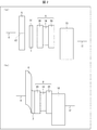
- FIG. 3 is an energy band diagram showing an example of a Fermi level or band gap of each layer in the light emitting device according to Embodiment 1 of the present disclosure.
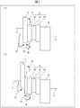
- FIG. 6 is an energy band diagram of each layer in the light emitting device according to the comparative example and the light emitting device according to the first embodiment of the present disclosure, for explaining the effect of the light emitting device according to the first embodiment of the present disclosure.
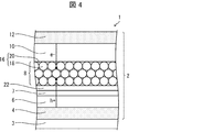
- FIG. 5 is a schematic cross-sectional view of a light emitting device according to a second embodiment of the present disclosure.
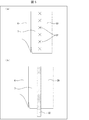
- FIG. 6 is an enlarged view of energy band diagrams of respective layers in the light emitting device according to the comparative form and the light emitting device according to the second embodiment of the present disclosure, for explaining the effect of the light emitting device according to the second embodiment of the present disclosure.
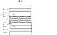
- FIG. 6 is a schematic cross-sectional view of a light emitting device according to Embodiment 3 of the present disclosure.
- FIG. 6 is an enlarged view of energy band diagrams of respective layers in a light emitting device according to a comparative example and a light emitting device according to embodiment 3 of the present disclosure, for explaining effects of the light emitting device according to embodiment 3 of the present disclosure.
- FIG. 1 is a schematic sectional view of a light emitting device 1 according to this embodiment.
- the light emitting device 1 includes a light emitting element 2 and an array substrate 3.
- the light emitting device 1 has a structure in which each layer of the light emitting element 2 is laminated on an array substrate 3 on which a TFT (Thin Film Transistor) (not shown) is formed.
- TFT Thin Film Transistor
- the light emitting element 2 includes a hole transport layer 6, an n-type semiconductor layer 7, a light emitting layer 8, an electron transport layer 10, and a cathode 12 on the anode 4 in this order from the lower layer.
- the anode 4 of the light emitting element 2 formed on the upper layer of the array substrate 3 is electrically connected to the TFT of the array substrate 3.
- a cathode is provided in an upper layer of the array substrate, and an electron transport layer, a light emitting layer, an n-type semiconductor layer, a hole transport layer, and an anode are provided on the cathode. It may be a light emitting element provided in order.
- the anode 4 and the cathode 12 include a conductive material and are electrically connected to the hole transport layer 6 and the electron transport layer 10, respectively.
- Either one of the anode 4 and the cathode 12 is a transparent electrode.
- the transparent electrode for example, ITO, IZO, ZnO, AZO, BZO or the like is used, and the transparent electrode may be formed by a sputtering method or the like.
- the anode 4 or the cathode 12 may contain a metallic material, and the metallic material is preferably Al, Cu, Au, Ag or the like having a high reflectance of visible light.
- the light emitting layer 8 is a layer containing a plurality of quantum dots (semiconductor nanoparticles) 16.
- the light emitting layer 8 may be a stack of several light emitting layers.
- the quantum dots 16 in the light emitting layer 8 do not need to be regularly arranged as shown in FIG. 1, and the quantum dots 16 may be randomly included in the light emitting layer 8.
- the light emitting layer 8 can be formed into a film by a spin coating method, an inkjet method, or the like from a dispersion liquid in which the quantum dots 16 are dispersed in a solvent such as hexane or toluene.
- a dispersion material such as thiol or amine may be mixed with the dispersion liquid.
- the thickness of the light emitting layer 8 is preferably 5 to 50 nm.
- Quantum dot 16 is a light emitting material that has a valence band level and a conduction band level, and emits light by recombination of holes in the valence band level and electrons in the conduction band level. Since the light emitted from the quantum dots 16 has a narrow spectrum due to the quantum confinement effect, it is possible to obtain light emission with a relatively deep chromaticity.
- the quantum dot 16 has a core/shell structure having a core 18 and a shell 20 which is an outer shell of the core 18.
- the core 18 is a semiconductor material particle having a bandgap within the bandgap of the shell 20.
- the core 18 may include a II-IV group semiconductor material or a III-V group semiconductor material.
- the shell 20 includes a II-IV type semiconductor material.
- the quantum dots 16 may have CdSe in the core and ZnS in the shell, for example.
- the quantum dots 16 may be appropriately selected from materials used in the field, and have, for example, CdSe/CdS, InP/ZnS, ZnSe/ZnS, or CIGS/ZnS as a core/shell structure. May be.
- the particle size of the quantum dots 16 is about 3 to 15 nm.
- the wavelength of light emitted from the quantum dots 16 can be controlled by the particle size of the core 18. Therefore, by controlling the particle size of the core 18, the wavelength of the light emitted by the light emitting device 1 can be controlled.
- the light emitting layer 8 may further include a ligand that forms a coordinate bond with the shell 20 of the quantum dot 16.
- the hole transport layer 6 is a layer that transports holes from the anode 4 to the light emitting layer 8.
- the hole transport layer 6 is a p-type semiconductor layer.
- the hole transport layer 6 contains an oxide of any one of the IIA group, the VIB group, and the VIIIB group. That is, the hole transport layer 6 contains an oxide of an element of any one of Groups 6, 8-10, and 12.
- the hole transport layer 6 is a p-type semiconductor layer containing at least one of MgO, Cr 2 O 3 and NiO.
- Each layer of the hole transport layer 6 may be formed by a sputtering method.
- the thickness of the hole transport layer 6 is preferably 5 to 40 nm.
- the hole transport layer 6 has a function of blocking electrons transported from the light emitting layer 8 toward the anode 4. Therefore, the electron affinity of the hole transport layer 6 is preferably smaller than the electron affinity of the shell 20 of the light emitting layer 8.
- the electron transport layer 10 is a layer that transports electrons from the cathode 12 to the light emitting layer 8.
- the electron transport layer 10 may have a function of inhibiting the transport of holes.
- the electron transport layer 10 may include, for example, ZnO, TiO 2 , Ta 2 O 3 , SrTiO 3 , or the like, and may be formed by a sputtering method.
- the film thickness of the electron transport layer 10 may be a conventionally known film thickness, and is preferably 10 to 100 nm.
- the light emitting element 2 in the present embodiment includes the n-type semiconductor layer 7 between the hole transport layer 6 and the light emitting layer 8.
- the n-type semiconductor layer 7 includes a first semiconductor material that is a II-IV group semiconductor material.
- the first semiconductor material may include ZnS, ZnSe, or CdS.
- the II-IV group type semiconductor material included in the shell 20 is referred to as a second semiconductor material.
- the first semiconductor material is the same as the second semiconductor material.
- the first semiconductor material has a group II element belonging to a lower period in the periodic table than the group II element contained in the second semiconductor material.
- the n-type semiconductor 7 may contain Zn or Cd.
- the n-type semiconductor layer 7 includes a Group 13 element as a dopant.
- the group 13 element contained in the n-type semiconductor layer 7 contains, for example, at least one of B, Al, Ga, and In.
- the concentration of the group 13 element in the n-type semiconductor layer 7 is 10 16 cm ⁇ 3 to 10 22 cm ⁇ 3 . That is, in this embodiment, the n-type semiconductor layer 7 is an n+-type semiconductor layer. In the semiconductor layer 7, the concentration of the group 13 element may be higher from the light emitting layer 8 side toward the hole transport layer 6 side.
- the n-type semiconductor layer 7 is formed, for example, by forming a film on the light emitting layer 8 or the hole transporting layer 6 by a sputtering method using a material to which n-type impurities are previously doped as a target. Further, the n-type semiconductor layer 7 may be formed, for example, by applying a nano-particle-shaped n-type semiconductor material. The n-type semiconductor layer 7 may be formed by performing the above-mentioned sputtering method while doping the n-type impurities.
- FIG. 2A is an energy band diagram showing an example of the Fermi level or the band gap when the respective layers of the light emitting device 2 according to the present embodiment are not laminated.
- the energy band diagram in this specification shows the energy level of each layer based on the vacuum level. Further, in the energy band diagram of this specification, the Fermi level or band gap of a member corresponding to the attached member number is shown. The Fermi level is shown for the anode 4 and the cathode 12, and the band gap from the electron affinity to the ionization potential is shown for the hole transport layer 6, the n-type semiconductor layer 7, the light emitting layer 8, and the electron transport layer 10. Here, the light emitting layer 8 is divided into the core 18 and the shell 20, and the respective band gaps are shown.
- the hole transport layer 6 contains NiO
- the ionization potential of the hole transport layer 6 is 5.6 eV and the electron affinity of the hole transport layer 6 is 2.1 eV.
- the electron transport layer 10 contains ZnO
- the ionization potential of the electron transport layer 10 is 7.0 eV and the electron affinity of the electron transport layer 10 is 3.8 eV.
- the shell 20 contains ZnS
- the ionization potential in the shell 20 is 5.2 eV and the electron affinity is 3.2 eV.
- Examples 1 to 10 examples of combinations of materials of the respective layers in the present embodiment are shown in Examples 1 to 10 in Table 1.
- Table 1 examples of combinations of materials of the respective layers in the present embodiment are shown in Examples 1 to 10 in Table 1.
- all the respective levels are based on the vacuum level, and eV is shown as a unit.
- Table 1 numerical values in a state where each layer is not laminated are described.
- FIG. 2B is an energy band diagram showing an example of the Fermi level or the band gap when the respective layers of the light emitting device 2 according to the present embodiment are laminated.
- the Fermi level or the band gap of the anode 4 the light emitting layer 8, the electron transport layer 10 and the cathode 12 is almost different from each level in the single state. do not do.
- the hole transport layer 6 and the n-type semiconductor layer 7 make a pn junction, and therefore, as shown in FIG. The electron affinity and the ionization potential of each of the semiconductor layers 7 change.
- the band structure of the hole transport layer 6 is band-shifted to the n-type semiconductor layer 7 side by the above-mentioned pn junction. That is, the electron affinity and the ionization potential of the hole transport layer 6 decrease from the n-type semiconductor layer 7 side toward the anode 4 side. Similarly, the electron affinity and ionization potential of the n-type semiconductor layer 7 decrease from the hole transport layer 6 side toward the light emitting layer 8 side.
- the concentration of carriers in the hole transport layer 6 is 10 16 cm ⁇ 3 to 10 22 cm ⁇ 3 with respect to the entire volume of the hole transport layer 6. That is, in the present embodiment, by stacking the hole transport layer 6 and the n-type semiconductor layer 7, the depletion layer spreads widely on the side of the hole transport layer 6 that is the p ⁇ type semiconductor layer.
- the carrier density of the n-type semiconductor layer 7 alone is much higher than the carrier density of the hole transport layer 6 alone. Therefore, the electron affinity and ionization potential of each of the hole transport layer 6 and the n-type semiconductor layer 7 due to the pn junction between the hole transport layer 6 and the n-type semiconductor layer 7 are Changes greatly.
- the electron affinity and the ionization potential of the hole transport layer 6 increase from the interface between the hole transport layer 6 and the n-type semiconductor layer 7 to the interface between the hole transport layer 6 and the anode 4. Is changing.
- the electron affinity and the ionization potential of the n-type semiconductor layer 7 change slightly only near the interface between the hole transport layer 6 and the n-type semiconductor layer 7.
- the amount of change between the electron affinity and the ionization potential of the hole transport layer 6 and the n-type semiconductor layer 7 due to the pn junction of the hole transport layer 6 and the n-type semiconductor layer 7 is positive before the pn junction. This corresponds to the difference in Fermi level between the hole transport layer 6 and the n-type semiconductor layer 7.
- the Fermi level 6f of the single hole transport layer 6 shown by the dotted line in FIG. 2A can be regarded as the center of the band gap. Further, since the carrier density of the n-type semiconductor layer 7 alone is very high, the Fermi level 7f of the n-type semiconductor layer 7 alone shown by the dotted line in (a) of FIG. It can be regarded as the same value as the electron affinity.
- the hole transport layer 6 and the n-type semiconductor layer 7 are pn-junctioned, the carriers of the n-type semiconductor layer 7 flow into the hole transport layer 6 side, so that the hole transport layer 6 and the n-type semiconductor layer 7 respectively.
- the Fermi levels of are averaged.
- the amount of change between the electron affinity and the ionization potential of each of the hole transport layer 6 and the n-type semiconductor layer 7 depends on the level at the center of the band gap of the hole transport layer 6 and the electrons of the n-type semiconductor layer 7. It can be estimated that this is the difference from the affinity.
- the effect of the light emitting element 2 according to the present embodiment will be described by comparing the energy band diagram of the light emitting element according to the comparative embodiment shown in FIG. 3 with the energy band diagram of the light emitting element 2 according to the present embodiment.
- FIG. 3 is an energy band diagram of each layer of the light emitting device according to the comparative form.
- the light emitting device according to the comparative embodiment differs from the light emitting device 2 according to the present embodiment only in that the n-type semiconductor layer 7 is not provided. Therefore, it can be considered that the levels of the layers of the light emitting device according to the comparative embodiment are the same as the levels of a single element before the layers of the light emitting device 2 according to the present embodiment are stacked.
- the electron transport layer 6 when the electron affinity of the hole transport layer 6 is larger than the electron affinity of the shell 20, the electron transport is further carried to the hole transport layer 6 via the shell 20 as shown by an arrow E1 in FIG. The electrons that are done are blocked. As a result, the concentration of electrons remaining in the light emitting layer 8 is increased and the light emission efficiency is improved.
- the difference between the Fermi level of the anode 4 and the ionization potential of the hole transport layer 6 is relatively large. Therefore, in FIG. 3A, the barrier for hole injection from the anode 4 to the hole transport layer 6 shown by the arrow H1 becomes relatively large.
- the ionization potential of the hole transport layer 6 is larger than the ionization potential of the shell 20. Therefore, the hole concentration in the hole transport layer 6 is relatively low. Therefore, in the light emitting device according to the comparative embodiment, hole injection from the hole transport layer 6 to the shell 20, which is indicated by an arrow H2 in FIG. 3A, that is, in FIG. It is difficult for electrons to be extracted from the shell 20 to the hole transport layer 6 as indicated by an arrow E2.
- the hole injection efficiency into the light emitting layer 8 is reduced due to the hole injection barrier described above. Therefore, the carrier balance in the light emitting layer 8 becomes poor, and the non-light emitting process in the light emitting layer 8 increases, so that the external quantum efficiency of the entire light emitting element deteriorates.
- a material having a smaller band gap may be adopted as the material of the hole transport layer 6.
- simply reducing the band gap of the hole transport layer 6 makes it difficult for the hole transport layer 6 to block the electron transport from the light emitting layer 8 to the anode 4, thus improving the external quantum efficiency of the light emitting device. It may not lead to.
- FIG. 3B is an energy band diagram of each layer of the light emitting element 2 according to this embodiment.
- the hole injection from the hole transport layer 6 to the shell 20 is caused by the holes tunneling through the n-type semiconductor layer 7 due to the tunnel effect generated in the n-type semiconductor layer 7.
- the electron affinity of the hole transport layer 6 is increased by the pn junction between the hole transport layer 6 and the n-type semiconductor layer 7. Therefore, the hole transport layer 6 maintains the function of blocking the electron transport from the light emitting layer 8 to the anode 4 as indicated by the arrow E1 in FIG.
- the pn junction between the hole transport layer 6 and the n-type semiconductor layer 7 greatly reduces the ionization potential on the anode 4 side of the hole transport layer 6. Therefore, in FIG. 3B, the barrier for hole injection from the anode 4 to the hole transport layer 6 shown by the arrow H1 becomes small.
- the pn junction between the hole transport layer 6 and the n-type semiconductor layer 7 also reduces the ionization potential of the hole transport layer 6 on the n-type semiconductor layer 7 side. Therefore, the concentration of holes in the hole transport layer 6 increases. Therefore, the hole injection from the hole transport layer 6 to the shell 20 shown by the arrow H2 in FIG. 3B, that is, from the shell 20 shown by the arrow E2 in FIG. Electrons are easily extracted to the hole transport layer 6.
- the efficiency of transporting holes from the anode 4 to the light emitting layer 8 is improved as described above. Therefore, the carrier balance in the light emitting layer 8 is improved and the light emitting process in the light emitting layer 8 is increased, so that the external quantum efficiency of the entire light emitting element 2 is improved.
- Table 2 shows the difference in ionization potential between the hole transport layer 6 and the shell 20 and the difference in electron affinity between the hole transport layer 6 and the shell 20 in the light emitting element 2 according to the present embodiment.
- 4 is a table comparing before and after stacking of FIG.
- the unit of numerical values in Table 2 is eV, and each example in Table 2 corresponds to each example in Table 1.
- the column of “difference in ionization potential” shows a value obtained by subtracting the ionization potential with the shell 20 from the ionization potential of the hole transport layer 6 before and after lamination.
- the negative value in the “difference in ionization potential” column indicates that the ionization potential of the hole transport layer 6 is smaller than that of the shell 20.
- the column of “difference in electron affinity” shows a value obtained by subtracting the electron affinity of the hole transport layer 6 from the electron affinity of the shell 20 before and after lamination. That is, the numerical value in the “difference in electron affinity” column corresponds to an electron transport barrier for blocking electron transport from the light emitting layer 8 to the anode 4.
- the negative value in the “difference in electron affinity” column indicates that the electron affinity of the hole transport layer 6 is larger than the electron affinity of the shell 20.
- the column of “level change amount” shows the amount of change in electron affinity and ionization potential of the hole transport layer 6 and the n-type semiconductor layer 7 after lamination. As described above, it is estimated that the amount of change in the electron affinity and the ionization potential described above corresponds to the difference between the level at the center of the band gap of the hole transport layer 6 and the electron affinity of the n-type semiconductor layer 7. Then, the numerical value in the "level change" column is calculated.
- the numerical value in the column of “ionization potential” after the lamination is decreased and the numerical value in the column of “electron affinity” is increased after the lamination, as compared with that before the lamination. .. This is because the concentration of holes in the hole transport layer 6 increases after stacking as compared with that before stacking, and an electron transport barrier for blocking electron transport from the light emitting layer 8 to the anode 4 is formed. It shows that it has become higher.
- the material of the n-type semiconductor layer 7 is the same as the material of the shell 20 in any of the examples.
- the material of the n-type semiconductor layer 7 is preferably a II-IV group type semiconductor material having a group II element belonging to a lower period in the periodic table than the group II element contained in the material of the shell 20. ..
- the II-IV group semiconductor that is the n-type semiconductor layer 7 contains an element having an ionic radius larger than that of the material of the shell 20.
- the bond of valence orbits is relatively weak, the energy at the top of the valence band, that is, the ionization potential becomes small, and the hole injection from the hole transport layer 6 to the shell 20 is further reduced. Barriers are reduced.
- the n-type semiconductor layer 7 is an n+-type semiconductor layer.
- the concentration of the group 13 element that is the dopant of the n-type semiconductor layer 7 is 10 16 cm ⁇ 3 or more.
- the concentration of the dopant in the n-type semiconductor layer 7 is sufficiently high, the above-mentioned changes in the ionization potential and the electron affinity of the hole transport layer 6 sufficiently occur.
- the concentration of the group 13 element which is the dopant of the n-type semiconductor layer 7 is 10 22 cm ⁇ 3 or less.
- the concentration of the group 13 element which is the dopant of the n-type semiconductor layer 7 is 10 22 cm ⁇ 3 or less.
- the thickness of the n-type semiconductor layer 7 is preferably 1 nm or more from the viewpoint of forming the n-type semiconductor layer 7 more reliably and reducing the carrier traps in the n-type semiconductor layer 7.
- the film thickness of the n-type semiconductor layer 7 is preferably 5 nm or less so that the tunnel effect of holes in the n-type semiconductor layer 7 can be sufficiently obtained.
- FIG. 4 is a schematic cross-sectional view of the light emitting device 1 according to this embodiment.
- the light emitting device 1 according to this embodiment is the same as the light emitting device 1 according to the previous embodiment except that a non-conductive layer 22 is provided between the n-type semiconductor layer 7 and the light emitting layer 8. It has the configuration of.
- the non-conductor layer 22 includes a non-conductor that has almost no carriers and points to an object having extremely poor electrical conductivity. Nonconductors are also commonly referred to as insulators or dielectrics. Specifically, for example, the non-conductive layer 22 includes at least one selected from the group consisting of Al 2 O 3 , SiN, SiO 2, SiON, and Cr 2 O 3 . The non-conductive layer 22 is in contact with both the n-type semiconductor layer 7 and the light emitting layer 8.
- the hole injection from the n-type semiconductor layer 7 to the shell 20 is caused by the holes tunneling through the non-conductive layer 22 due to the tunnel effect generated in the non-conductive layer 22.
- .. 5A and 5B are energy band diagrams of the light emitting device 2 according to the previous embodiment and the present embodiment, respectively, in which only the vicinity of the ionization potential from the hole transport layer 6 to the shell 20 is extracted. It is the enlarged view shown.
- the n-type semiconductor layer 7 and the light emitting layer 8 are in direct contact with each other.
- the contact between the n-type semiconductor layer 7 and the light emitting layer 8 is a contact between semiconductors.
- the laminated structure is not manufactured by using epitaxial growth. Therefore, in the present embodiment, it is difficult to avoid generation of levels on the surface and interface of each layer of the light emitting element 2. Therefore, an interface state is formed at the interface between the n-type semiconductor layer 7 and the shell 20.
- a carrier trap CT is formed at the interface between the n-type semiconductor layer 7 and the shell 20, as shown in FIG.
- the nonconductor layer 22 is formed between the n-type semiconductor layer 7 and the light emitting layer 8.
- the contact between the n-type semiconductor layer 7 and the non-conductor layer 22 and the contact between the non-conductor layer 22 and the light-emitting layer 8 are both the contact between the semiconductor and the non-conductor.
- the interface order is inactivated at the interface between the n-type semiconductor layer 7 and the non-conductive layer 22 and the interface between the non-conductive layer 22 and the light emitting layer 8, and eventually carrier trap CT occurs. Can be reduced. Therefore, the holes transported from the anode 4 are less likely to be trapped in the carrier trap CT, so that the carrier balance in the light emitting layer 8 is further improved.
- the thickness of the non-conductive layer 22 is preferably 1 nm or more from the viewpoint of forming the non-conductive layer 22 more reliably and reducing carrier traps in the non-conductive layer 22.
- the thickness of the non-conductive layer 22 is preferably 5 nm or less so that the tunnel effect of holes in the non-conductive layer 22 can be sufficiently obtained.
- FIG. 6 is a schematic cross-sectional view of the light emitting device 1 according to this embodiment.
- the light emitting device 1 according to the present embodiment is different from the light emitting device 1 according to each of the above-described embodiments in that the non-conductive layer 22 is provided between the hole transport layer 6 and the n-type semiconductor layer 7. Except for this, it has the same configuration.
- the non-conductive layer 22 may have the same configuration as the non-conductive layer 22 of the light emitting device 1 according to the previous embodiment.
- the hole injection from the hole transport layer 6 to the n-type semiconductor layer 7 is caused by the holes tunneling through the non-conductive layer 22 due to the tunnel effect generated in the non-conductive layer 22.
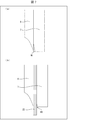
- .. 7A and 7B are energy band diagrams of the light emitting device 2 according to the first embodiment and the light emitting device 2 according to the present embodiment, showing only the vicinity of the ionization potential from the hole transport layer 6 to the n-type semiconductor layer 7, respectively. It is the enlarged view which extracted and illustrated.
- the pn junction between the hole transport layer 6 and the n-type semiconductor layer 7 causes a change in the ionization potential not only in the hole transport layer 6 but also in the n-type semiconductor layer 7. Has occurred.
- the carrier density of the n-type semiconductor layer 7 is higher than that of the hole-transporting layer 6, the change of the ionization potential in the pn junction n-type semiconductor layer 7 is small and the hole-transporting layer is It occurs only in the vicinity of the contact interface with 6.
- the potential well W1 shown in FIG. It is formed on the n-type semiconductor layer 7 side of the interface between the hole transport layer 6 and the n-type semiconductor layer 7, the potential well W1 shown in FIG. It is formed.
- the holes transported from the anode 4 may be trapped in the potential well W1. Therefore, in the light emitting element 2 according to the first embodiment, the concentration of holes transported to the light emitting layer 8 may decrease, and the carrier balance in the light emitting layer 8 may deteriorate.
- the nonconductor layer 22 is provided between the hole transport layer 6 and the n-type semiconductor layer 7. Therefore, the hole transport layer 6 and the n-type semiconductor layer 7 are not in direct contact with each other, and the carrier transfer from the n-type semiconductor layer 7 to the hole transport layer 6 is realized through the non-conductive layer 22.
- the change in the ionization potential in the n-type semiconductor layer 7 due to the pn junction is smaller than that in the case where the hole transport layer 6 and the n-type semiconductor layer 7 are directly in the pn junction.
- the change in the ionization potential of the n-type semiconductor layer 7 is smaller than that of the n-type semiconductor layer 7 of the light emitting device 2 according to the first embodiment, and the contact with the hole transport layer 6 is smaller. It occurs only at positions close to the interface.
- the potential well generated at the interface between the hole transport layer 6 and the n-type semiconductor layer 7 becomes the potential well W2 shown in FIG. 7B.
- the potential well W2 has a smaller region formed and a shallower depth than the potential well W1. Therefore, as compared with the first embodiment, in the present embodiment, the possibility that holes transported from the anode 4 are trapped in the potential well W2 can be reduced. Therefore, the carrier balance in the light emitting layer 8 is further improved.
- the light emitting element 2 according to the present embodiment may further include a non-conductive layer 22 between the n-type semiconductor layer 7 and the light emitting layer 8.
- a non-conductive layer 22 between the n-type semiconductor layer 7 and the light emitting layer 8.
Landscapes
- Electroluminescent Light Sources (AREA)
- Led Devices (AREA)
Abstract
発光素子(2)は、アノード(4)と、p型半導体層である正孔輸送層(6)と、13族元素を含むn型半導体層(7)と、量子ドット(16)を含む発光層(8)と、電子輸送層(10)と、カソード(12)とを、この順に備える。
Description
本開示は、発光層に量子ドットを含む発光素子、および当該発光素子を備えた発光デバイスに関する。
特許文献1には、半導体ナノクリスタルを含む発光素子を備えた発光デバイスが開示されている。
特許文献1においては、正孔輸送層にNiOを使用している。しかしながら、正孔輸送層としてNiO等の従来の材料を備えた、発光層に量子ドットを含む発光素子は、十分な電子ブロック性と発光層への正孔注入効率とを両立することが困難である。
上記課題を解決するために、本開示の発光素子は、アノードと、p型半導体層である正孔輸送層と、13族元素を含むn型半導体層と、量子ドットを含む発光層と、電子輸送層と、カソードとを、この順に備える。
上記構成により、電子ブロック性を担保しつつ、発光層への正孔注入効率を改善した発光素子を提供できる。
〔実施形態1〕
本明細書においては、元素の族をローマ数字にて指定している場合には、旧CAS方式の命名法に基づいた族の指定を行っているものとする。また、元素の族をアラビア数字にて指定している場合には、現行のIUPAC方式の元素の命名法に基づいた族の指定を行っているものとする。
本明細書においては、元素の族をローマ数字にて指定している場合には、旧CAS方式の命名法に基づいた族の指定を行っているものとする。また、元素の族をアラビア数字にて指定している場合には、現行のIUPAC方式の元素の命名法に基づいた族の指定を行っているものとする。
図1は、本実施形態に係る発光デバイス1の概略断面図である。
図1に示すように、本実施形態に係る発光デバイス1は、発光素子2とアレイ基板3とを備える。発光デバイス1は、図示しないTFT(Thin Film Transistor)が形成されたアレイ基板3上に、発光素子2の各層が積層された構造を備える。なお、本明細書においては、発光デバイス1の発光素子2からアレイ基板3への方向を「下方向」、発光素子2のアレイ基板3から発光素子2への方向を「上方向」として記載する。
発光素子2は、アノード4上に、正孔輸送層6と、n型半導体層7と、発光層8と、電子輸送層10と、カソード12とを、下層からこの順に備える。アレイ基板3の上層に形成された発光素子2のアノード4は、アレイ基板3のTFTと電気的に接続されている。他の実施形態に係る発光素子においては、アレイ基板の上層にカソードを備え、カソード上に、電子輸送層と、発光層と、n型半導体層と、正孔輸送層と、アノードとを、この順に備える発光素子であってもよい。
アノード4およびカソード12は導電性材料を含み、それぞれ、正孔輸送層6および電子輸送層10と電気的に接続されている。
アノード4とカソード12との何れか一方は、透明電極である。透明電極としては、例えば、ITO、IZO、ZnO、AZO、またはBZO等が用いられ、スパッタ法等によって成膜されてもよい。また、アノード4またはカソード12のいずれか一方は金属材料を含んでいてもよく、金属材料としては、可視光の反射率の高いAl、Cu、Au、またはAg等が好ましい。
発光層8は、複数の量子ドット(半導体ナノ粒子)16を含む層である。発光層8は、数層の発光層が積層したものであってもよい。ここで、発光層8における量子ドット16は、図1に示すように、規則正しく配置されている必要はなく、量子ドット16は無秩序に発光層8に含まれていてもよい。発光層8は、ヘキサンまたはトルエン等の溶媒に量子ドット16を分散させた分散液から、スピンコート法、またはインクジェット法等によって製膜することができる。分散液にはチオール、アミン等分散材料を混合してもよい。発光層8の膜厚は、5~50nmが好ましい。
量子ドット16は、価電子帯準位と伝導帯準位とを有し、価電子帯準位の正孔と伝導帯準位の電子との再結合によって発光する発光材料である。量子ドット16からの発光は、量子閉じ込め効果により狭いスペクトルを有するため、比較的深い色度の発光を得ることが可能である。
本実施形態において、量子ドット16は、コア18と、当該コア18の外殻であるシェル20とを有する、コア/シェル構造を備えている。コア18は、シェル20のバンドギャップの範囲内にバンドギャップが含まれる半導体材料粒子である。コア18は、II-IV族型半導体材料、あるいは、III-V族型半導体材料を含んでいてもよい。シェル20は、II-IV族型半導体材料を含んでいる。
量子ドット16は、例えば、コアにCdSe、シェルにZnSを備えていてもよい。この他、量子ドット16は、当該分野において利用される材料から適宜選択されてもよく、例えば、CdSe/CdS、InP/ZnS、ZnSe/ZnSまたはCIGS/ZnS等をコア/シェル構造として有していてもよい。
量子ドット16の粒径は3~15nm程度である。量子ドット16からの発光の波長は、コア18の粒径によって制御することができる。このため、コア18の粒径を制御することにより、発光デバイス1が発する光の波長を制御できる。なお、発光層8は、さらに、量子ドット16のシェル20と配位結合するリガンドを備えていてもよい。
正孔輸送層6は、アノード4からの正孔を発光層8へと輸送する層である。本実施形態において、正孔輸送層6はp型半導体層である。また、正孔輸送層6は、IIA族、VIB族、およびVIIIB族の内の何れかの元素の酸化物を含む。すなわち、正孔輸送層6は、6族、8~10族、および12族の内の何れかの元素の酸化物を含む。例えば、正孔輸送層6は、MgO、Cr2O3、または、NiOの内、少なくとも何れかを含むp型半導体層である。正孔輸送層6の各層は、スパッタ法によって製膜されてもよい。正孔輸送層6の膜厚は、5~40nmが好ましい。
本実施形態においては、正孔輸送層6は、発光層8からアノード4へ向かって輸送される電子をブロックする機能を備えている。このため、正孔輸送層6の電子親和力は、発光層8のシェル20の電子親和力よりも小さいことが好ましい。
電子輸送層10は、カソード12からの電子を発光層8へと輸送する層である。電子輸送層10は、正孔の輸送を阻害する機能を有していてもよい。電子輸送層10は、例えば、ZnO、TiO2、Ta2O3、またはSrTiO3等を含んでいてもよく、スパッタ法によって製膜されてもよい。電子輸送層10の膜厚は、従来公知の膜厚を採用でき、10~100nmが好ましい。
本実施形態における発光素子2は、正孔輸送層6と発光層8との間に、n型半導体層7を備える。n型半導体層7は、II-IV族型半導体材料である第1半導体材料を含む。第1半導体材料は、ZnS、ZnSe、またはCdSを含んでいてもよい。
ここで、シェル20が含むII-IV族型半導体材料を第2半導体材料とする。この場合、第1半導体材料は、第2半導体材料と同一である。あるいは、第1半導体材料は、第2半導体材料に含まれるII族元素よりも、周期表において下位の周期に属するII族元素を有する。例えば、シェル20がZnを含む場合、n型半導体7は、ZnまたはCdを含んでいてもよい。
また、n型半導体層7は13族元素をドーパントとして備えている。n型半導体層7が含む13族元素は、例えば、B、Al、Ga、およびInの少なくとも1種を含む。n型半導体層7における13族元素の濃度は、1016cm-3~1022cm-3である。すなわち、本実施形態において、n型半導体層7は、n+型半導体層である。なお、半導体層7においては、13族元素の濃度が、発光層8側から正孔輸送層6側に向かって高くなっていてもよい。
n型半導体層7は、例えば、予めn型不純物をドープした材料をターゲットとしたスパッタ法により、発光層8上または正孔輸送層6上に成膜することにより形成される。また、n型半導体層7は、例えば、ナノ粒子化したn型半導体材料を塗布することにより形成してもよい。なお、n型半導体層7は、上述のスパッタ法を、n型不純物をドープしつつ実行することにより形成してもよい。
次に、本実施形態に係る発光素子2の各層におけるエネルギーバンドについて、図2を参照して説明する。
図2の(a)は、本実施形態に係る発光素子2の各層を積層しない場合におけるフェルミ準位、またはバンドギャップの例を示すエネルギーバンド図である。
なお、本明細書のエネルギーバンド図においては、各層の、真空準位を基準としたエネルギー準位を示している。また、本明細書のエネルギーバンド図においては、付した部材番号と対応する部材のフェルミ準位、またはバンドギャップを示す。アノード4およびカソード12についてはフェルミ準位を、正孔輸送層6、n型半導体層7、発光層8、および電子輸送層10については、電子親和力からイオン化ポテンシャルまでのバンドギャップをそれぞれ示す。ここで、発光層8については、コア18とシェル20とに分けて、それぞれのバンドギャップを示す。
本実施形態において、例えば、正孔輸送層6がNiOを含む場合、正孔輸送層6のイオン化ポテンシャルは5.6eVであり、正孔輸送層6の電子親和力は2.1eVである。また、本実施形態において、例えば、電子輸送層10がZnOを含む場合、電子輸送層10のイオン化ポテンシャルは7.0eVであり、電子輸送層10の電子親和力は3.8eVである。また、本実施形態において、例えば、シェル20がZnSを含む場合、シェル20におけるイオン化ポテンシャルは5.2eVであり、電子親和力は3.2eVである。
ここで、本実施形態における、各層の材料の組み合わせの例を、表1の実施例1から実施例10に示す。なお、表1における「イオン化ポテンシャル」、および「電子親和力」の欄は、それぞれの準位を、全て真空準位を基準とし、eVを単位として示す。また、表1においては、各層を積層しない状態における数値を記載している。

図2の(b)は、本実施形態に係る発光素子2の各層を積層した場合におけるフェルミ準位、またはバンドギャップの例を示すエネルギーバンド図である。
本実施形態においては、各層を積層した発光素子2において、アノード4、発光層8、電子輸送層10、およびカソード12のフェルミ準位、またはバンドギャップは、単体の状態の各準位とほとんど変化しない。しかしながら、各層を積層した発光素子2においては、正孔輸送層6とn型半導体層7とがpn接合するために、図2の(b)に示すように、正孔輸送層6とn型半導体層7とのそれぞれの電子親和力とイオン化ポテンシャルとが変化する。
具体的には、上述のpn接合により、正孔輸送層6のバンド構造が、n型半導体層7側にバンドシフトする。すなわち、正孔輸送層6の電子親和力とイオン化ポテンシャルとは、n型半導体層7側からアノード4側に向かって小さくなる。同様に、n型半導体層7の電子親和力とイオン化ポテンシャルとは、正孔輸送層6側から発光層8側に向かって小さくなる。
正孔輸送層6とn型半導体層7とがpn接合した際、電荷中性条件を満足するために、正孔輸送層6に向かってn型半導体層7のキャリアが多量に流入する。このため、正孔輸送層6におけるキャリアの濃度は、正孔輸送層6全体の体積に対して、1016cm-3~1022cm-3となる。すなわち、本実施形態において、正孔輸送層6が、n型半導体層7と積層することにより、p-型半導体層である正孔輸送層6側に、広く空乏層が広がる。
n型半導体層7単体のキャリア密度は、正孔輸送層6単体のキャリア密度と比較して非常に大きい。このため、正孔輸送層6とn型半導体層7とのpn接合に起因する、正孔輸送層6とn型半導体層7とのそれぞれの電子親和力とイオン化ポテンシャルとは、正孔輸送層6の方が大きく変化する。
具体的には、正孔輸送層6の電子親和力とイオン化ポテンシャルとは、正孔輸送層6とn型半導体層7との界面から正孔輸送層6とアノード4との界面に渡って、大きく変化している。対して、n型半導体層7の電子親和力とイオン化ポテンシャルとは、正孔輸送層6とn型半導体層7との界面付近においてのみ、小さく変化する。
正孔輸送層6とn型半導体層7とのpn接合による、正孔輸送層6とn型半導体層7とのそれぞれの電子親和力とイオン化ポテンシャルとの変化量は、pn接合をする前の正孔輸送層6とn型半導体層7とのそれぞれのフェルミ準位の差に相当する。
正孔輸送層6単体のキャリア密度は非常に低いため、図2の(a)に点線にて示す、正孔輸送層6単体のフェルミ準位6fは、おおよそバンドギャップの中心とみなせる。また、n型半導体層7単体のキャリア密度は非常に大きいため、図2の(a)に点線にて示す、n型半導体層7単体のフェルミ準位7fは、非常に電子親和力に近く、おおよそ電子親和力と同値であるとみなせる。正孔輸送層6とn型半導体層7とがpn接合すると、n型半導体層7のキャリアが正孔輸送層6側に流れ込むことにより、正孔輸送層6とn型半導体層7とのそれぞれのフェルミ準位が平均化される。
したがって、正孔輸送層6とn型半導体層7とのそれぞれの電子親和力とイオン化ポテンシャルとの変化量は、正孔輸送層6のバンドギャップの中心の準位と、n型半導体層7の電子親和力との差であることが推定できる。
本実施形態に係る発光素子2の効果について、図3に示す、比較形態に係る発光素子のエネルギーバンド図と、本実施形態に係る発光素子2のエネルギーバンド図とを比較して説明する。
図3の(a)は、比較形態に係る発光素子の各層のエネルギーバンド図である。比較形態に係る発光素子は、n型半導体層7を備えていない点においてのみ、本実施形態に係る発光素子2と構成が異なる。したがって、比較形態に係る発光素子の各層の準位は、本実施形態に係る発光素子2の各層を積層する前の、単体の準位とそれぞれ同一であると見なせる。
比較形態に係る発光素子のアノード4とカソード12との間に電位差が生じると、アノード4側から正孔輸送層6へ正孔が、カソード12側から電子輸送層10へ電子が注入される。その後、正孔輸送層6に注入された正孔と電子輸送層10に注入された電子とは、発光層8の量子ドット16のシェル20を介して、コア18まで到達する。コア18において、正孔と電子とが再結合することにより、励起子が生成される。
ここで、正孔輸送層6の電子親和力は、シェル20の電子親和力よりも大きい場合、図3の(a)の矢印E1に示すように、さらにシェル20を介して正孔輸送層6に輸送される電子がブロックされる。これにより、発光層8にとどまる電子の濃度が高くなり、発光効率が改善する。
しかしながら、比較形態においては、アノード4のフェルミ準位と、正孔輸送層6のイオン化ポテンシャルとの差が比較的大きい。このため、図3の(a)において、矢印H1にて示す、アノード4から正孔輸送層6への正孔注入の障壁が比較的大きくなる。
さらに、比較形態においては、正孔輸送層6のイオン化ポテンシャルが、シェル20のイオン化ポテンシャルよりも大きい。このために、正孔輸送層6における正孔の濃度が比較的低くなっている。このため、比較形態に係る発光素子においては、図3の(a)において、矢印H2にて示す、正孔輸送層6からシェル20への正孔注入、すなわち、図3の(a)において、矢印E2にて示す、シェル20から正孔輸送層6への電子の引き抜きが発生しにくい。
したがって、比較形態に係る発光素子においては、上述した正孔注入の障壁のために、発光層8への正孔の注入効率が低減する。ゆえに、発光層8におけるキャリアバランスが悪くなり、発光層8における非発光過程が増大するために、発光素子全体の外部量子効率が悪化する。
正孔注入の効率を改善するのみであれば、正孔輸送層6の材料に、バンドギャップのより小さい材料を採用すればよい。しかしながら、正孔輸送層6のバンドギャップを単純に小さくするのみでは、発光層8からアノード4への電子輸送を、正孔輸送層6がブロックしにくくなるため、発光素子の外部量子効率の改善につながらない場合がある。
図3の(b)は、本実施形態に係る発光素子2の各層のエネルギーバンド図である。本実施形態に係る発光素子2においても、比較形態に係る発光素子と同様に、正孔と電子との輸送が生じ、発光層8における励起子の生成が発生する。ただし、正孔輸送層6からシェル20への正孔注入は、n型半導体層7において生じるトンネル効果によって、正孔がn型半導体層7をトンネルすることにより生じる。
本実施形態においては、正孔輸送層6とn型半導体層7とのpn接合により、正孔輸送層6の電子親和力が増大している。このため、図3の(a)の矢印E1にて示す、発光層8からアノード4への電子輸送をブロックする機能を、正孔輸送層6が維持する。
本実施形態においては、正孔輸送層6とn型半導体層7とのpn接合により、正孔輸送層6のアノード4側のイオン化ポテンシャルが大きく低減している。このため、図3の(b)において、矢印H1にて示す、アノード4から正孔輸送層6への正孔注入の障壁が小さくなる。
さらに、正孔輸送層6とn型半導体層7とのpn接合により、正孔輸送層6のn型半導体層7側のイオン化ポテンシャルについても低減している。このため、正孔輸送層6における正孔の濃度が増加する。したがって、図3の(b)において、矢印H2にて示す、正孔輸送層6からシェル20への正孔注入、すなわち、図3の(b)において、矢印E2にて示す、シェル20から正孔輸送層6への電子の引き抜きが発生しやすくなる。
したがって、本実施形態に係る発光素子2においては、上述したように、アノード4から発光層8への正孔の輸送効率が改善する。ゆえに、発光層8におけるキャリアバランスが改善し、発光層8における発光過程が増大するために、発光素子2全体の外部量子効率が改善する。
表2は、本実施形態に係る発光素子2における、正孔輸送層6とシェル20とのイオン化ポテンシャルの差と、正孔輸送層6とシェル20との電子親和力の差とを、発光素子2の積層前と積層後とにおいて比較した表である。なお、表2における数値の単位は何れもeVであり、表2における各実施例は、表1の各実施例に対応する。
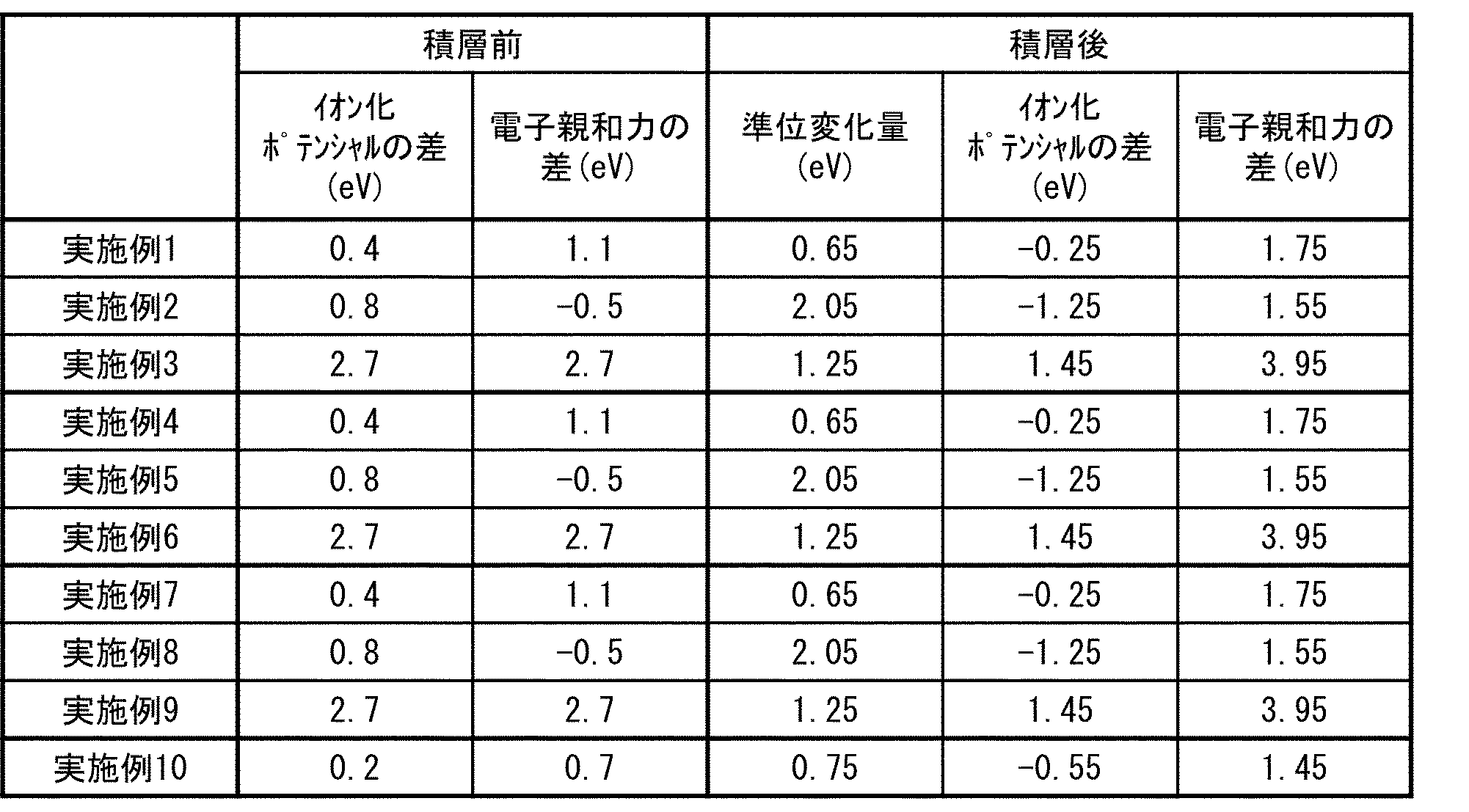
「電子親和力の差」の欄は、積層前と積層後とのそれぞれにおける、シェル20の電子親和力から正孔輸送層6の電子親和力を引いた値を示す。すなわち、「電子親和力の差」の欄の数値は、発光層8からアノード4への電子輸送をブロックするための、電子輸送の障壁に相当する。「電子親和力の差」の欄の数値が負であることは、正孔輸送層6の電子親和力が、シェル20との電子親和力よりも大きいことを示す。
「準位変化量」の欄は、積層後の正孔輸送層6とn型半導体層7とのそれぞれの電子親和力とイオン化ポテンシャルとの変化量を示す。なお、上述したように、上述した電子親和力とイオン化ポテンシャルとの変化量は、正孔輸送層6のバンドギャップの中心の準位と、n型半導体層7の電子親和力との差に相当すると推定し、「準位変化量」の欄の数値を算出している。
表2に示すように、何れの実施例においても、積層前と比較して、積層後における、「イオン化ポテンシャル」の欄の数値は減少し、「電子親和力」の欄の数値は増加している。これは、積層前と比較して、積層後においては、正孔輸送層6における正孔の濃度が増大し、発光層8からアノード4への電子輸送をブロックするための、電子輸送の障壁が高くなったことを示している。
本実施形態においては、何れの実施例においても、n型半導体層7の材料は、シェル20の材料と同一の材料である。しかしながら、n型半導体層7の材料は、シェル20の材料に含まれるII族元素よりも、周期表において下位の周期に属するII族元素を有する、II-IV族型半導体材料であることが好ましい。当該構成によれば、n型半導体層7であるII-IV族型半導体は、シェル20の材料よりイオン半径が大きい元素を含む。したがって、n型半導体層7においては、価電子軌道の結合が相対的に弱く、価電子帯頂上のエネルギー、すなわちイオン化ポテンシャルが小さくなり、より正孔輸送層6からシェル20への正孔注入の障壁が低減される。
本実施形態において、n型半導体層7は、n+型半導体層である。特に、n型半導体層7のドーパントである13族元素の濃度は、1016cm-3以上である。このため、n型半導体層7におけるドーパントの濃度が十分に高いため、上述した正孔輸送層6のイオン化ポテンシャルおよび電子親和力の変化が十分に生じる。また、n型半導体層7に含まれるII-IV型半導体の結晶組成の変化を防止する観点から、n型半導体層7のドーパントである13族元素の濃度は、1022cm-3以下であることが好ましい。
本実施形態において、n型半導体層7をより確実に成膜し、n型半導体層7におけるキャリアトラップを低減する観点から、n型半導体層7の膜厚は1nm以上であることが好ましい。また、本実施形態において、n型半導体層7における正孔のトンネル効果が十分に得られるように、n型半導体層7の膜厚は5nm以下であることが好ましい。
〔実施形態2〕
図4は、本実施形態に係る発光デバイス1の概略断面図である。本実施形態に係る発光デバイス1は、前実施形態に係る発光デバイス1と比較して、n型半導体層7と発光層8との間に、不導体層22を備えた点を除いて、同一の構成を有する。
図4は、本実施形態に係る発光デバイス1の概略断面図である。本実施形態に係る発光デバイス1は、前実施形態に係る発光デバイス1と比較して、n型半導体層7と発光層8との間に、不導体層22を備えた点を除いて、同一の構成を有する。
不導体層22は、キャリアをほとんど有さず、電気伝導性が著しく乏しい物体を指す不導体を含む。不導体は、一般に、絶縁体または誘電体とも呼称される。具体的には、例えば、不導体層22は、Al2O3、SiN、SiO2、SiON、およびCr2O3から構成された群の内、少なくとも1種を含む。不導体層22は、n型半導体層7と発光層8との双方と接触している。
本実施形態に係る発光素子2においても、前実施形態に係る発光素子2と同様に、正孔と電子との輸送が生じ、発光層8における励起子の生成が発生する。ただし、n型半導体層7からシェル20への正孔注入は、不導体層22において生じるトンネル効果によって、正孔が不導体層22をトンネルすることにより生じる。
本実施形態に係る発光素子2の効果について、図5に示す、前実施形態に係る発光素子2のエネルギーバンド図と、本実施形態に係る発光素子2のエネルギーバンド図とを比較して説明する。図5の(a)および(b)は、それぞれ、前実施形態および本実施形態に係る発光素子2のエネルギーバンド図を、正孔輸送層6からシェル20までの、イオン化ポテンシャル付近のみを抜き出して図示した拡大図である。
前実施形態においては、n型半導体層7と発光層8とが直接接している。ここで、n型半導体層7と発光層8と接触は、半導体同士の接触である。また、本実施形態に係る発光素子2においては、一般的な無機半導体発光素子のように、エピタキシャル成長を用いて積層構造を作製しない。したがって、本実施形態においては、発光素子2の各層の表面および界面における準位の発生を避けることが困難である。このため、n型半導体層7とシェル20との界面においては、界面準位が形成される。
したがって、n型半導体層7とシェル20との界面においては、図5の(a)に示すように、キャリアトラップCTが形成される。キャリアトラップCTに、アノード4から輸送されてきた正孔がトラップされると、発光層8に輸送される正孔の濃度が低減し、発光層8におけるキャリアバランスが悪化する場合がある。
一方、実施形態においては、図5の(b)に示すように、n型半導体層7と発光層8との間に、不導体層22が形成されている。n型半導体層7と不導体層22との接触、および不導体層22と発光層8との接触は、いずれも半導体と不導体との接触となる。
このため、本実施形態においては、n型半導体層7と不導体層22との界面、および不導体層22と発光層8と界面において、界面順位を不活性化し、ひいては、キャリアトラップCTが生じることを低減できる。したがって、アノード4から輸送されてきた正孔が、キャリアトラップCTにトラップされることが低減されるため、発光層8におけるキャリアバランスがさらに改善する。
本実施形態において、不導体層22をより確実に成膜し、不導体層22におけるキャリアトラップを低減する観点から、不導体層22の膜厚は1nm以上であることが好ましい。また、本実施形態において、不導体層22における正孔のトンネル効果が十分に得られるように、不導体層22の膜厚は5nm以下であることが好ましい。
〔実施形態3〕
図6は、本実施形態に係る発光デバイス1の概略断面図である。本実施形態に係る発光デバイス1は、前述した各実施形態に係る発光デバイス1と比較して、正孔輸送層6とn型半導体層7との間に、不導体層22を備えた点を除いて、同一の構成を有する。不導体層22は、前実施形態に係る発光デバイス1の不導体層22と同一の構成を有していてもよい。
図6は、本実施形態に係る発光デバイス1の概略断面図である。本実施形態に係る発光デバイス1は、前述した各実施形態に係る発光デバイス1と比較して、正孔輸送層6とn型半導体層7との間に、不導体層22を備えた点を除いて、同一の構成を有する。不導体層22は、前実施形態に係る発光デバイス1の不導体層22と同一の構成を有していてもよい。
本実施形態に係る発光素子2においても、前述した各実施形態に係る発光素子2と同様に、正孔と電子との輸送が生じ、発光層8における励起子の生成が発生する。ただし、正孔輸送層6からn型半導体層7への正孔注入は、不導体層22において生じるトンネル効果によって、正孔が不導体層22をトンネルすることにより生じる。
本実施形態に係る発光素子2の効果について、図7に示す、実施形態1に係る発光素子2のエネルギーバンド図と、本実施形態に係る発光素子2のエネルギーバンド図とを比較して説明する。図7の(a)および(b)は、それぞれ、実施形態1および本実施形態に係る発光素子2のエネルギーバンド図を、正孔輸送層6からn型半導体層7までの、イオン化ポテンシャル付近のみを抜き出して図示した拡大図である。
実施形態1に係る発光素子2においては、正孔輸送層6とn型半導体層7とのpn接合により、正孔輸送層6のみならず、n型半導体層7においても、イオン化ポテンシャルの変化が生じている。ここで、正孔輸送層6と比較して、n型半導体層7のキャリアの密度は高いため、上述のpn接合n型半導体層7におけるイオン化ポテンシャルの変化は、小さく、かつ、正孔輸送層6との接触界面の近傍においてのみ発生する。
このため、正孔輸送層6とn型半導体層7との界面のn型半導体層7側において、図7の(a)に示す、周囲よりもイオン化ポテンシャルが小さい領域である、ポテンシャル井戸W1が形成される。ポテンシャル井戸W1には、アノード4から輸送された正孔がトラップされる場合がある。ゆえに、実施形態1に係る発光素子2においては、発光層8に輸送される正孔の濃度が低減し、発光層8におけるキャリアバランスが悪化する場合がある。
一方、本実施形態に係る発光素子2においては、正孔輸送層6とn型半導体層7との間に、不導体層22を備えている。このため、正孔輸送層6とn型半導体層7とは直接接触せず、n型半導体層7から正孔輸送層6へのキャリアの移動が、不導体層22を介して実現する。
したがって、正孔輸送層6とn型半導体層7とが直接pn接合している場合と比較して、当該pn接合による、n型半導体層7におけるイオン化ポテンシャルの変化が小さくなる。具体的には、n型半導体層7におけるイオン化ポテンシャルの変化は、実施形態1に係る発光素子2のn型半導体層7と比較して、より小さく、かつ、より正孔輸送層6との接触界面の近接する位置においてのみ発生する。
このため、正孔輸送層6とn型半導体層7との界面に生じるポテンシャル井戸は、図7の(b)に示すポテンシャル井戸W2となる。上記理由から、ポテンシャル井戸W2はポテンシャル井戸W1よりも、形成される領域が小さく、かつ、井戸の深さが浅い。このため、実施形態1と比較して、本実施形態においては、アノード4から輸送された正孔が、ポテンシャル井戸W2にトラップされる可能性を低減できる。ゆえに、発光層8におけるキャリアバランスがさらに改善する。
本実施形態に係る発光素子2は、前実施形態に係る発光素子2と同様に、さらに、n型半導体層7と発光層8との間においても、不導体層22を備えていてもよい。当該構成により、n型半導体層7と発光層8との間における、正孔のトラップについても低減することができ、発光層8のキャリアバランスがより改善される。
本開示は上述した各実施形態に限定されるものではなく、請求項に示した範囲で種々の変更が可能であり、異なる実施形態にそれぞれ開示された技術的手段を適宜組み合わせて得られる実施形態についても本開示の技術的範囲に含まれる。さらに、各実施形態にそれぞれ開示された技術的手段を組み合わせることにより、新しい技術的特徴を形成することができる。
1 発光デバイス
2 発光素子
4 アノード
6 正孔輸送層
7 n型半導体層
8 発光層
10 電子輸送層
12 カソード
16 量子ドット
20 シェル
22 不導体層
2 発光素子
4 アノード
6 正孔輸送層
7 n型半導体層
8 発光層
10 電子輸送層
12 カソード
16 量子ドット
20 シェル
22 不導体層
Claims (15)
- アノードと、p型半導体層である正孔輸送層と、13族元素を含むn型半導体層と、量子ドットを含む発光層と、電子輸送層と、カソードとを、この順に備えた発光素子。
- 前記n型半導体層が、II-IV族型半導体材料である第1半導体材料を含む請求項1に記載の発光素子。
- 前記量子ドットが、コア/シェル構造を有し、前記量子ドットのシェルが、II-IV族型半導体材料である第2半導体材料を含む請求項2に記載の発光素子。
- 前記第1半導体材料が、前記第2半導体材料と同一、あるいは、前記第2半導体材料に含まれるII族元素よりも、周期表において下位の周期に属するII族元素を有する、II-IV族型半導体材料である請求項3に記載の発光素子。
- 前記n型半導体が、B、Al、Ga、およびInから選択される少なくとも1種の13族元素を含む請求項1から4の何れか1項に記載の発光素子。
- 前記n型半導体における前記13族元素の濃度が、1016cm-3~1022cm-3である請求項1から5の何れか1項に記載の発光素子。
- 前記n型半導体の膜厚が、1nm以上5nm以下である請求項1から6の何れか1項に記載の発光素子。
- 前記n型半導体と前記発光層との間に、不導体を含む不導体層をさらに備えた請求項1から7の何れか1項に記載の発光素子。
- 前記n型半導体と前記正孔輸送層との間に、不導体を含む不導体層をさらに備えた請求項1から7の何れか1項に記載の発光素子。
- 前記不導体層の膜厚が、1nm以上5nm以下である請求項8または9に記載の発光素子。
- 前記不導体が、Al2O3、SiN、SiO2、SiON、およびCr2O3から構成された群の内、少なくとも1種を含む請求項8から10の何れか1項に記載の発光素子。
- 前記正孔輸送層が、IIA族の酸化物、VIB族の酸化物、VIIIB族の酸化物のいずれかを含む請求項1から11の何れか1項に記載の発光素子。
- 前記正孔輸送層が、MgO、Cr2O3、または、NiOの内、少なくとも何れかを含む請求項1から12の何れか1項に記載の発光素子。
- 前記正孔輸送層におけるキャリアの濃度が、1016cm-3~1022cm-3である請求項1から13の何れか1項に記載の発光素子。
- 請求項1から14の何れか1項に記載の発光素子を備えた発光デバイス。
Priority Applications (3)
| Application Number | Priority Date | Filing Date | Title |
|---|---|---|---|
| PCT/JP2018/045361 WO2020121381A1 (ja) | 2018-12-10 | 2018-12-10 | 発光素子、発光デバイス |
| CN201880100165.2A CN113196880B (zh) | 2018-12-10 | 2018-12-10 | 发光元件、发光设备 |
| US17/311,861 US12040429B2 (en) | 2018-12-10 | 2018-12-10 | Light-emitting element and light-emitting device |
Applications Claiming Priority (1)
| Application Number | Priority Date | Filing Date | Title |
|---|---|---|---|
| PCT/JP2018/045361 WO2020121381A1 (ja) | 2018-12-10 | 2018-12-10 | 発光素子、発光デバイス |
Publications (1)
| Publication Number | Publication Date |
|---|---|
| WO2020121381A1 true WO2020121381A1 (ja) | 2020-06-18 |
Family
ID=71076832
Family Applications (1)
| Application Number | Title | Priority Date | Filing Date |
|---|---|---|---|
| PCT/JP2018/045361 Ceased WO2020121381A1 (ja) | 2018-12-10 | 2018-12-10 | 発光素子、発光デバイス |
Country Status (3)
| Country | Link |
|---|---|
| US (1) | US12040429B2 (ja) |
| CN (1) | CN113196880B (ja) |
| WO (1) | WO2020121381A1 (ja) |
Families Citing this family (3)
| Publication number | Priority date | Publication date | Assignee | Title |
|---|---|---|---|---|
| WO2021064822A1 (ja) * | 2019-09-30 | 2021-04-08 | シャープ株式会社 | 発光素子、発光デバイス |
| US20220325178A1 (en) * | 2021-03-30 | 2022-10-13 | Samsung Electronics Co., Ltd. | Quantum dot device and electronic device |
| CN116632134B (zh) * | 2023-07-24 | 2023-10-10 | 江西乾照光电有限公司 | 一种电子阻挡层及其制备方法、外延片及发光二极管 |
Citations (7)
| Publication number | Priority date | Publication date | Assignee | Title |
|---|---|---|---|---|
| US20110080090A1 (en) * | 2009-05-07 | 2011-04-07 | Massachusetts Institute Of Technology | Light emitting device including semiconductor nanocrystals |
| JP2012023388A (ja) * | 2005-02-16 | 2012-02-02 | Massachusetts Inst Of Technol <Mit> | 半導体ナノクリスタルを含む発光デバイス |
| US20130015424A1 (en) * | 2011-07-14 | 2013-01-17 | Samsung Electronics Co., Ltd. | Optoelectronic devices |
| JP2016058172A (ja) * | 2014-09-08 | 2016-04-21 | 一般財団法人電力中央研究所 | 発光素子および電子機器 |
| CN106450018A (zh) * | 2016-11-01 | 2017-02-22 | Tcl集团股份有限公司 | Qled及其制备方法 |
| US20170271605A1 (en) * | 2016-03-17 | 2017-09-21 | Apple Inc. | Quantum dot spacing for high efficiency quantum dot led displays |
| US20180331312A1 (en) * | 2015-11-04 | 2018-11-15 | Guangzhou Chinaray Optoelectronic Materials Ltd. | Electroluminescent device, preparation method thereof, and ink formulation |
Family Cites Families (17)
| Publication number | Priority date | Publication date | Assignee | Title |
|---|---|---|---|---|
| US20070001581A1 (en) * | 2005-06-29 | 2007-01-04 | Stasiak James W | Nanostructure based light emitting devices and associated methods |
| JP2010225563A (ja) * | 2009-03-25 | 2010-10-07 | Panasonic Electric Works Co Ltd | 有機el素子 |
| KR101924080B1 (ko) * | 2009-11-11 | 2018-11-30 | 삼성 리서치 아메리카 인코포레이티드 | 양자점을 포함하는 디바이스 |
| KR20130065320A (ko) * | 2011-12-09 | 2013-06-19 | 삼성전자주식회사 | 이종의 양자점층을 구비하는 양자점 소자 |
| WO2014088667A2 (en) * | 2012-09-14 | 2014-06-12 | Qd Vision, Inc. | Light emitting device including tandem structure |
| JP6123438B2 (ja) * | 2013-04-05 | 2017-05-10 | コニカミノルタ株式会社 | 有機エレクトロルミネッセンス素子、それを具備した照明装置及び表示装置 |
| CN104638138A (zh) * | 2013-11-14 | 2015-05-20 | 海洋王照明科技股份有限公司 | 有机电致发光器件及其制备方法 |
| KR101772437B1 (ko) | 2014-12-03 | 2017-08-30 | 경희대학교 산학협력단 | 용액공정을 통해 형성된 전하 생성층을 사용한 발광 소자 및 이의 제조 방법 |
| KR20160081388A (ko) * | 2014-12-31 | 2016-07-08 | 엘지디스플레이 주식회사 | 유기전자장치 |
| KR102415248B1 (ko) * | 2015-12-29 | 2022-06-30 | 삼성디스플레이 주식회사 | 양자점 및 이를 이용한 발광 소자 |
| CN105552184A (zh) * | 2016-01-20 | 2016-05-04 | Tcl集团股份有限公司 | 一种全无机量子点发光二极管及其制备方法 |
| CN105470387A (zh) | 2016-01-25 | 2016-04-06 | 深圳市华星光电技术有限公司 | 量子点发光器件及其制备方法及液晶显示装置 |
| US10700236B2 (en) * | 2016-03-17 | 2020-06-30 | Apple Inc. | Quantum dot spacing for high efficiency quantum dot LED displays |
| KR102374223B1 (ko) * | 2017-09-19 | 2022-03-14 | 엘지디스플레이 주식회사 | 다중 발광 양자점과 이를 포함하는 양자점 필름, 엘이디 패키지, 발광다이오드 및 표시장치 |
| KR102355917B1 (ko) * | 2017-10-26 | 2022-01-25 | 엘지디스플레이 주식회사 | 발광다이오드 및 전계발광 표시장치 |
| KR102593358B1 (ko) * | 2018-08-14 | 2023-10-25 | 쑤저우 레킨 세미컨덕터 컴퍼니 리미티드 | 발광소자 패키지 및 광원 장치 |
| KR102696329B1 (ko) * | 2018-10-30 | 2024-08-19 | 엘지디스플레이 주식회사 | 양자점 필름, 엘이디 패키지, 발광다이오드 및 표시장치 |
-
2018
- 2018-12-10 CN CN201880100165.2A patent/CN113196880B/zh active Active
- 2018-12-10 WO PCT/JP2018/045361 patent/WO2020121381A1/ja not_active Ceased
- 2018-12-10 US US17/311,861 patent/US12040429B2/en active Active
Patent Citations (7)
| Publication number | Priority date | Publication date | Assignee | Title |
|---|---|---|---|---|
| JP2012023388A (ja) * | 2005-02-16 | 2012-02-02 | Massachusetts Inst Of Technol <Mit> | 半導体ナノクリスタルを含む発光デバイス |
| US20110080090A1 (en) * | 2009-05-07 | 2011-04-07 | Massachusetts Institute Of Technology | Light emitting device including semiconductor nanocrystals |
| US20130015424A1 (en) * | 2011-07-14 | 2013-01-17 | Samsung Electronics Co., Ltd. | Optoelectronic devices |
| JP2016058172A (ja) * | 2014-09-08 | 2016-04-21 | 一般財団法人電力中央研究所 | 発光素子および電子機器 |
| US20180331312A1 (en) * | 2015-11-04 | 2018-11-15 | Guangzhou Chinaray Optoelectronic Materials Ltd. | Electroluminescent device, preparation method thereof, and ink formulation |
| US20170271605A1 (en) * | 2016-03-17 | 2017-09-21 | Apple Inc. | Quantum dot spacing for high efficiency quantum dot led displays |
| CN106450018A (zh) * | 2016-11-01 | 2017-02-22 | Tcl集团股份有限公司 | Qled及其制备方法 |
Also Published As
| Publication number | Publication date |
|---|---|
| US12040429B2 (en) | 2024-07-16 |
| CN113196880A (zh) | 2021-07-30 |
| CN113196880B (zh) | 2024-09-17 |
| US20220020898A1 (en) | 2022-01-20 |
Similar Documents
| Publication | Publication Date | Title |
|---|---|---|
| US10147844B2 (en) | Quantum dot and light emitting diode including the same | |
| US11349094B2 (en) | Organic light emitting diode and organic light emitting diode display device including the same | |
| CN109148704B (zh) | 量子点电致发光器件及其制备方法 | |
| US11342524B2 (en) | Light emitting element, light emitting device, and apparatus for producing light emitting element | |
| KR20130000218A (ko) | 자성체 물질을 함유한 전극 및 상기 전극을 갖는 유기발광소자 | |
| US20240373663A1 (en) | Light-emitting element and light-emitting device | |
| US20170271552A1 (en) | Light emitting element and display device including the same | |
| US20260047235A1 (en) | Light-emitting element and light-emitting device | |
| WO2020134147A1 (zh) | 一种量子点发光二极管 | |
| WO2020121381A1 (ja) | 発光素子、発光デバイス | |
| WO2022137475A1 (ja) | 発光素子 | |
| CN112349853A (zh) | 电致发光器件及其制备方法和显示装置 | |
| US20220238830A1 (en) | Light-emitting element and light-emitting device | |
| CN112930607B (zh) | 发光元件 | |
| US20250248206A1 (en) | Light-emitting element and display device | |
| WO2021084598A1 (ja) | 発光素子 | |
| CN209912898U (zh) | 量子点发光二极管 | |
| CN110544746B (zh) | 发光二极管及其制备方法 | |
| US12550523B2 (en) | Method for manufacturing display device, and display device | |
| CN114695714B (zh) | 一种量子点发光二极管及其制备方法 | |
| US20120119185A1 (en) | Active layer for silicon light-emitting devices and method for manufacturing the same | |
| CN114695721A (zh) | 一种量子点发光二极管及其制备方法 | |
| WO2025257965A1 (ja) | 発光素子及び表示装置 | |
| CN114695704A (zh) | 一种量子点发光二极管及其制备方法 | |
| CN114695706A (zh) | 一种量子点发光二极管及其制备方法 |
Legal Events
| Date | Code | Title | Description |
|---|---|---|---|
| 121 | Ep: the epo has been informed by wipo that ep was designated in this application |
Ref document number: 18942913 Country of ref document: EP Kind code of ref document: A1 |
|
| NENP | Non-entry into the national phase |
Ref country code: DE |
|
| 122 | Ep: pct application non-entry in european phase |
Ref document number: 18942913 Country of ref document: EP Kind code of ref document: A1 |
|
| NENP | Non-entry into the national phase |
Ref country code: JP |