WO2020116282A1 - 保護膜形成用複合シート、及び半導体チップの製造方法 - Google Patents
保護膜形成用複合シート、及び半導体チップの製造方法 Download PDFInfo
- Publication number
- WO2020116282A1 WO2020116282A1 PCT/JP2019/046381 JP2019046381W WO2020116282A1 WO 2020116282 A1 WO2020116282 A1 WO 2020116282A1 JP 2019046381 W JP2019046381 W JP 2019046381W WO 2020116282 A1 WO2020116282 A1 WO 2020116282A1
- Authority
- WO
- WIPO (PCT)
- Prior art keywords
- protective film
- forming
- film
- composite sheet
- antistatic
- Prior art date
- Legal status (The legal status is an assumption and is not a legal conclusion. Google has not performed a legal analysis and makes no representation as to the accuracy of the status listed.)
- Ceased
Links
Images


Classifications
-
- B—PERFORMING OPERATIONS; TRANSPORTING
- B32—LAYERED PRODUCTS
- B32B—LAYERED PRODUCTS, i.e. PRODUCTS BUILT-UP OF STRATA OF FLAT OR NON-FLAT, e.g. CELLULAR OR HONEYCOMB, FORM
- B32B7/00—Layered products characterised by the relation between layers; Layered products characterised by the relative orientation of features between layers, or by the relative values of a measurable parameter between layers, i.e. products comprising layers having different physical, chemical or physicochemical properties; Layered products characterised by the interconnection of layers
- B32B7/02—Physical, chemical or physicochemical properties
- B32B7/025—Electric or magnetic properties
-
- H—ELECTRICITY
- H10—SEMICONDUCTOR DEVICES; ELECTRIC SOLID-STATE DEVICES NOT OTHERWISE PROVIDED FOR
- H10P—GENERIC PROCESSES OR APPARATUS FOR THE MANUFACTURE OR TREATMENT OF DEVICES COVERED BY CLASS H10
- H10P54/00—Cutting or separating of wafers, substrates or parts of devices
-
- H—ELECTRICITY
- H10—SEMICONDUCTOR DEVICES; ELECTRIC SOLID-STATE DEVICES NOT OTHERWISE PROVIDED FOR
- H10P—GENERIC PROCESSES OR APPARATUS FOR THE MANUFACTURE OR TREATMENT OF DEVICES COVERED BY CLASS H10
- H10P72/00—Handling or holding of wafers, substrates or devices during manufacture or treatment thereof
- H10P72/70—Handling or holding of wafers, substrates or devices during manufacture or treatment thereof for supporting or gripping
- H10P72/74—Handling or holding of wafers, substrates or devices during manufacture or treatment thereof for supporting or gripping using temporarily an auxiliary support
- H10P72/7402—Wafer tapes, e.g. grinding or dicing support tapes
-
- H—ELECTRICITY
- H10—SEMICONDUCTOR DEVICES; ELECTRIC SOLID-STATE DEVICES NOT OTHERWISE PROVIDED FOR
- H10P—GENERIC PROCESSES OR APPARATUS FOR THE MANUFACTURE OR TREATMENT OF DEVICES COVERED BY CLASS H10
- H10P72/00—Handling or holding of wafers, substrates or devices during manufacture or treatment thereof
- H10P72/70—Handling or holding of wafers, substrates or devices during manufacture or treatment thereof for supporting or gripping
- H10P72/74—Handling or holding of wafers, substrates or devices during manufacture or treatment thereof for supporting or gripping using temporarily an auxiliary support
- H10P72/7416—Handling or holding of wafers, substrates or devices during manufacture or treatment thereof for supporting or gripping using temporarily an auxiliary support used during dicing or grinding
-
- H—ELECTRICITY
- H10—SEMICONDUCTOR DEVICES; ELECTRIC SOLID-STATE DEVICES NOT OTHERWISE PROVIDED FOR
- H10W—GENERIC PACKAGES, INTERCONNECTIONS, CONNECTORS OR OTHER CONSTRUCTIONAL DETAILS OF DEVICES COVERED BY CLASS H10
- H10W99/00—Subject matter not provided for in other groups of this subclass
Definitions
- the present invention relates to a protective film forming composite sheet and a method for manufacturing a semiconductor chip.
- the present application claims priority based on Japanese Patent Application No. 2018-228528 filed in Japan on December 5, 2018, the contents of which are incorporated herein by reference.
- semiconductor devices have been manufactured using a mounting method called a so-called face down method.
- a semiconductor chip having electrodes such as bumps on the circuit surface is used, and the electrodes are bonded to the substrate. Therefore, the back surface of the semiconductor chip opposite to the circuit surface may be exposed.
- -A resin film containing an organic material is formed as a protective film on the exposed back surface of the semiconductor chip, and it may be incorporated into a semiconductor device as a semiconductor chip with a protective film.
- the protective film is used to prevent cracks from being generated in the semiconductor chip after the dicing process or packaging.
- a protective film-forming composite sheet configured by including a protective film forming film for forming a protective film on a support sheet.
- the protective film forming film can form a protective film by curing.
- the support sheet can be used for fixing the semiconductor wafer when the semiconductor wafer having the protective film forming film or the protective film on the back surface is divided into semiconductor chips.
- the support sheet can also be used as a dicing sheet, and the protective film-forming composite sheet can also be used as an integrated body of the protective film-forming film and the dicing sheet.
- the composite sheet for forming a protective film is used as follows. That is, first, the protective film-forming film in the protective film-forming composite sheet is attached to the back surface of the semiconductor wafer to obtain a laminate (hereinafter abbreviated as “pre-division laminate”).
- the protective film forming film in the pre-division laminate is cured to form a protective film, and the laminate (hereinafter abbreviated as “cured laminate”) is fixed on a dicing table.
- the pre-division laminate is fixed on a dicing table in a state where the protective film forming film in the pre-division laminate is not cured.
- cured laminated body in this laminated body fixed on the dicing table, the semiconductor wafer is divided, the protective film is cut, and the protective film after the cutting is formed on the support sheet. Then, a laminated body (hereinafter abbreviated as “cured and divided laminated body”) including the divided semiconductor wafer (that is, the semiconductor chip) in this order is obtained.
- the semiconductor wafer in this laminated body fixed on the dicing table, the semiconductor wafer is divided, the protective film forming film is cut, and it is cut on the support sheet.
- a laminated body (uncured and divided laminated body) provided with the protective film forming film and the semiconductor chip in this order is obtained. What is being done here is blade dicing, which is the mainstream.
- the protective film forming composite sheet is removed.
- the sheet may become charged. Since the protective film-forming composite sheet that is electrically charged is likely to adsorb small foreign matters on the protective film-forming film before being attached to the semiconductor wafer, the charged composite film for forming a protective film-forming film is not easily separated from the semiconductor wafer. In addition, foreign matter is easily mixed in.
- a supporting sheet, a protective film after cutting or a protective film-forming film, and a semiconductor chip And are laminated in this order to produce a laminated body. Then, when handling this laminated body, the operation is performed such that the laminated body is fixed on the table and then separated from the fixing surface on the table, but when the laminated body is separated from the table, Easy to be charged. If the laminate is charged, the circuit may be destroyed.
- a dicing tape (corresponding to the support sheet) in which a pressure-sensitive adhesive layer is laminated on a base material, and formed on the pressure-sensitive adhesive layer are disclosed.
- cured laminate etc. when fixing the cured laminate or the pre-division laminate (hereinafter abbreviated as “cured laminate etc.”) on a dicing table, protection of the cured laminate etc. Foreign matter may be attached to the outermost layer on the side of the film-forming composite sheet due to the influence of static electricity or the like, and between the cured laminate or the like and the dicing table (of the protective film-forming composite sheet and the dicing table). In the space), foreign matter is mixed in due to the influence of static electricity or the like, and the cured laminated body or the like cannot be placed horizontally, so that chipping (fine chipping) may occur.
- the dicing tape-integrated adhesive sheet disclosed in Patent Document 1 suppresses the generation of static electricity (peeling charge) between the adhesive sheet and the dicing tape, and suppresses the destruction of the circuit on the semiconductor element due to this static electricity. It is an object. Further, the surface resistivity of any surface of the dicing tape-integrated adhesive sheet is 1.0 ⁇ 10 11 ⁇ or less, and the surface resistance of the surface in contact with the dicing table is controlled. Therefore, it is not certain that it is possible to prevent the occurrence of chipping as described above. Further, the surface specific resistance value on any surface of the dicing tape-integrated adhesive sheet after heat-curing the dicing tape-integrated film for semiconductor back surface is also 1.0 ⁇ 10 11 ⁇ or less, or it is not clear. ..
- the present invention is a composite sheet for forming a protective film, comprising a support sheet and a film for forming a protective film, wherein, in dicing, foreign matter is mixed between the cured laminate and the dicing table due to static electricity or the like.
- the present embodiment is a protective film-forming composite sheet comprising a support sheet and a protective film-forming film formed on one surface of the support sheet, wherein the thermosetting protective film-forming composite sheet is used.
- the surface resistivity of the outermost layer on the side of the supporting sheet in the composite sheet for forming a protective film before heat curing of the film is 1.0 ⁇ 10 11 ⁇ / ⁇ or less, and for forming the thermosetting protective film.
- a composite sheet for forming a protective film, wherein the surface resistivity of the outermost layer on the side of the supporting sheet in the composite sheet for forming a protective film after heat curing of the film is 1.0 ⁇ 10 11 ⁇ / ⁇ or less. ..
- the support sheet comprises a base material and an antistatic layer formed on one or both surfaces of the base material, or the support sheet is
- the antistatic layer preferably has a base material having antistatic properties.
- it is preferable that the thickness of the antistatic layer formed on one side or both sides of the substrate is 100 nm or less.
- the support sheet preferably has a total light transmittance of 80% or more.
- the pressing surface of the pressing means having a flat pressing surface with an area of 2 cm ⁇ 2 cm is covered with flannel cloth, and the pressing surface covered with the flannel cloth is covered with the pressing surface.
- the pressing means is reciprocated 10 times at a linear distance of 10 cm.
- the present embodiment is a step of attaching the thermosetting protective film forming film in the protective film forming composite sheet to a semiconductor wafer, and the thermosetting protective film forming step after attaching to the semiconductor wafer.
- a method of manufacturing a semiconductor chip is provided.
- a protective film-forming composite sheet comprising a support sheet and a thermosetting protective film-forming film, in dicing, between the cured laminate or the like and the dicing table, such as static electricity
- a protective film-forming composite sheet and a method for manufacturing a semiconductor chip using the protective film-forming composite sheet, which prevent foreign matter from being mixed due to influences, and as a result, prevent chipping from occurring. To be done.
- FIG. 6 is a cross-sectional view for schematically explaining the method for manufacturing a semiconductor chip according to the embodiment of the present invention.
- FIG. 6 is a cross-sectional view for schematically explaining the method for manufacturing a semiconductor chip according to the embodiment of the present invention.
- FIG. 6 is a cross-sectional view for schematically explaining the method for manufacturing a semiconductor chip according to the embodiment of the present invention.
- a composite sheet for forming a protective film according to an embodiment of the present invention comprises a supporting sheet and a thermosetting protective film forming film formed on one surface of the supporting sheet. It is a composite sheet for forming a protective film, before heat curing of the thermosetting protective film forming film, in the protective film forming composite sheet, the surface resistivity of the outermost layer of the support sheet side. 1.0 ⁇ 10 11 ⁇ / ⁇ or less, and the surface resistivity of the outermost surface layer on the support sheet side in the protective film-forming composite sheet after heat curing of the thermosetting protective film-forming film. It is 1.0 ⁇ 10 11 ⁇ / ⁇ or less.
- the surface resistivity of the composite film for forming a protective film is 1.0 ⁇ 10 11 ⁇ / ⁇ or less. Therefore, it is possible to prevent foreign matter from adhering to the outermost surface layer on the support sheet side in the protective film forming composite sheet due to the influence of static electricity or the like. As a result, chipping can be prevented from occurring during dicing.
- the surface resistivity is 1.0 ⁇ 10 11 ⁇ / ⁇ or less both before and after heat curing of the thermosetting protective film-forming film. Also when performing dicing before heat curing, also when performing dicing after heat curing the thermosetting protective film forming film, due to the influence of static electricity or the like, in the protective film forming composite sheet, the support It is possible to prevent foreign matter from adhering to the outermost layer on the sheet side. As a result, chipping can be prevented from occurring during dicing.
- the term “surface resistivity of the protective film-forming composite sheet” means the surface resistivity of the outermost layer on the supporting sheet side in the above-mentioned protective film-forming composite sheet, unless otherwise specified.
- the “film for forming a protective film” means a film for forming a thermosetting protective film, unless otherwise specified.
- the protective film-forming composite sheet of the present embodiment has a normal-time charge suppressing effect because any of the layers therein contains an antistatic agent.
- the degree of the effect of suppressing the normal charging in other words, the high surface resistivity is, for example, a layer containing an antistatic agent (in the present specification, comprehensively). It can be adjusted by selecting the type of the antistatic agent (which may be referred to as “antistatic layer”) or adjusting the content.
- the surface resistivity of the protective film-forming composite sheet before the thermosetting of the protective film-forming film in the protective film-forming composite sheet is 1.0 ⁇ 10 11 ⁇ / ⁇ or less. Among them, it is preferably 9.5 ⁇ 10 10 ⁇ / ⁇ or less, for example, 5.0 ⁇ 10 10 ⁇ / ⁇ or less, 6.0 ⁇ 10 9 ⁇ / ⁇ or less, and 1.0 ⁇ 10 9 It may be either ⁇ / ⁇ or less.
- the surface resistivity is equal to or lower than the upper limit value, it is possible to prevent foreign matter from adhering to the outermost surface layer on the support sheet side in the protective film forming composite sheet due to the influence of static electricity or the like. it can. As a result, chipping can be prevented from occurring during dicing.
- the lower limit of the surface resistivity of the protective film-forming composite sheet before the protective film-forming film is heat-cured is preferably as small as possible, and is not particularly limited.
- a composite sheet for forming a protective film, in which the surface resistivity before heat curing is 1.0 ⁇ 10 5 ⁇ / ⁇ or more, can be more easily manufactured.
- the surface resistivity of the protective film-forming composite sheet before the protective film-forming film is heat-cured can be appropriately adjusted within the range set by arbitrarily combining the preferable lower limit value and the preferable upper limit value described above.
- the surface resistivity before heat curing is preferably 1.0 ⁇ 10 5 to 5.0 ⁇ 10 10 ⁇ / ⁇ , for example, 1.0 ⁇ 10 5 to 6. It may be any of 0 ⁇ 10 9 ⁇ / ⁇ , 1.0 ⁇ 10 5 to 5.0 ⁇ 10 8 ⁇ / ⁇ , and 1.0 ⁇ 10 5 to 3.0 ⁇ 10 8 ⁇ / ⁇ . .. However, these are examples of the surface resistivity before heat curing.
- the surface resistivity of the protective film-forming composite sheet after the thermosetting of the protective film-forming film in the protective film-forming composite sheet is 1.0 ⁇ 10 11 ⁇ / ⁇ or less.
- the above-mentioned surface resistivity condition for example, preferable upper limit value or lower limit value
- the protective film forming composite sheet in the composite sheet for forming a protective film is at 130° C. for 2 hours. It is preferably thermoset.
- the surface resistivity after the film for forming a protective film in the composite sheet for forming a protective film is thermoset at 130° C. for 2 hours, Those having a resistance of 1.0 ⁇ 10 11 ⁇ / ⁇ or less are included.
- this is an example of the composite sheet for forming a protective film, which satisfies the above-described surface resistivity condition.
- the surface resistivity is less than or equal to the upper limit value, even after the protective film-forming film in the protective film-forming composite sheet has been thermoset, foreign matter due to the influence of static electricity or the like is a protective film-forming composite sheet. Can be prevented from adhering to the outermost layer on the side of the support sheet. As a result, chipping can be prevented from occurring during dicing.
- the surface resistivity of the protective film forming composite sheet is measured, using a surface resistivity meter, It can be measured with an applied voltage of 100V.
- the protective film forming composite sheet of the present embodiment is the above-mentioned condition of the surface resistivity after the protective film forming film is thermoset, and the surface resistivity of the protective film forming film before being thermoset. It is preferable that both the conditions and are satisfied.
- the support sheet may be composed of one layer (single layer) or may be composed of two or more layers.
- the constituent materials and thicknesses of the plurality of layers may be the same or different from each other, and the combination of the plurality of layers is not particularly limited as long as the effects of the present invention are not impaired.
- the support sheet may be transparent or opaque, and may be colored depending on the purpose.
- the supporting sheet is preferably transparent.
- the support sheet includes, for example, one including a base material and an adhesive layer formed on the base material; one including only the base material; and the like.
- the preferable supporting sheet includes, for example, a base material, and in the protective film-forming composite sheet, the supporting sheet is located on the opposite side of the base material from the protective film forming film side.
- a support sheet provided with an antistatic layer formed on the surface may be abbreviated as “backside antistatic layer” in the present specification); a base material having an antistatic property as the antistatic layer (the present specification In the specification, it may be abbreviated as “antistatic base material”); a support sheet comprising a base material, and in a composite film for forming a protective film, the above-mentioned protective film formation of the base material.
- a support sheet provided with an antistatic layer may be abbreviated as “surface antistatic layer” in the present specification) formed on the surface located on the film side is used.
- the antistatic layers back surface antistatic layer, antistatic substrate and surface antistatic layer
- the supporting sheet includes a base material, and an antistatic layer formed on one surface or both surfaces of the base material, a composite sheet for forming a protective film;
- An example of the protective sheet is a composite sheet for forming a protective film, in which the support sheet has a base material having antistatic properties (that is, an antistatic base material) as the antistatic layer.
- the “antistatic layer formed on one surface of the substrate” means the “backside antistatic layer or surface antistatic layer”.
- the "antistatic layer formed on both sides of the substrate” means "a combination of the backside antistatic layer and the surface antistatic layer”.
- the support sheet is a composite film for protective film formation comprising the substrate and the back surface antistatic layer, or the support sheet is a composite film for protective film formation comprising the antistatic substrate, preferable.
- the composite sheet for forming a protective film also includes a sheet having a layer that does not correspond to any of the back surface antistatic layer, the antistatic substrate, and the surface antistatic layer as an antistatic layer.
- the antistatic layer may be provided on the surface of the protective film forming film opposite to the support sheet side, or the protective film forming film may have antistatic properties.
- the antistatic layer that is, the supporting sheet side of the protective film forming film is The antistatic layer is incorporated in the semiconductor device after the antistatic layer provided on the opposite surface or the film for forming a protective film having antistatic property) is attached to the semiconductor chip.
- a protective film forming film or a protective film is attached to a semiconductor wafer or a semiconductor chip via an antistatic layer, or a protective film forming film having an antistatic property.
- the antistatic layer may adversely affect the stability of the structure of the semiconductor device or the performance of the semiconductor device.
- the antistatic layer may be provided on the surface of the protective film-forming film on the support sheet side.
- the protective film-forming film or the semiconductor chip to which the protective film is attached is separated from the antistatic layer on the support sheet and picked up. At this time, the process abnormality may occur due to the interposition of the antistatic layer.
- the protective film-forming composite sheet includes, as an antistatic layer, the back surface antistatic layer, the antistatic substrate, or the surface antistatic layer.
- FIG. 1 is a sectional view schematically showing a protective film-forming composite sheet according to an embodiment of the present invention.
- the protective film-forming composite sheet 101 shown here is a protective film formed on the support sheet 10 and one surface (sometimes referred to as “first surface” in the present specification) 10 a of the support sheet 10.
- the forming film 13 is provided.
- the support sheet 10 includes a base material 11, an adhesive layer 12 formed on one surface (sometimes referred to as “first surface” in this specification) 11 a of the base material 11, and the base material 11. And the back surface antistatic layer 17 formed on the other surface (which may be referred to as a "second surface” in the present specification) 11b. That is, the support sheet 10 is configured by laminating the back surface antistatic layer 17, the base material 11, and the adhesive layer 12 in this order in the thickness direction thereof.
- the first surface 10a of the support sheet 10 is a surface (which may be referred to as "first surface” in the present specification) of the pressure-sensitive adhesive layer 12 opposite to the base material 11 side.
- the protective film forming composite sheet 101 is configured by laminating the back surface antistatic layer 17, the base material 11, the adhesive layer 12, and the protective film forming film 13 in this order in the thickness direction thereof. ..
- the protective film forming composite sheet 101 further includes a release film 15 on the protective film forming film 13.
- the protective film forming film 13 is laminated on the entire surface or almost the entire first surface 12a of the adhesive layer 12, and the adhesive layer 12 side of the protective film forming film 13 is
- the adhesive layer 16 for a jig is laminated on a part of the opposite surface (which may be referred to as a “first surface” in the present specification) 13a, that is, a region in the vicinity of the peripheral edge to form a protective film.
- first surface 13a of the film 13 for jigs the surface on which the jig adhesive layer 16 is not laminated, and the surface of the jig adhesive layer 16 opposite to the pressure-sensitive adhesive layer 12 side (in the present specification, Is sometimes referred to as the “first surface”) 16a, and the release film 15 is laminated thereon.
- a gap may be partially formed between the release film 15 and the layer in direct contact with the release film 15.
- the state where the release film 15 is in contact (lamination) with the side surface 16c of the jig adhesive layer 16 is shown, but the release film 15 is not in contact with the side surface 16c.
- a state is shown in which the release film 15 is in contact (laminated) with a region near the jig adhesive layer 16 on the first surface 13a of the protective film forming film 13, The release film 15 may not be in contact with the area.
- the boundary between the first surface 16a and the side surface 16c of the jig adhesive layer 16 cannot be clearly distinguished.
- the protective film-forming composite sheet of the other embodiment which is provided with the jig adhesive layer.
- one or both surfaces of the base material are usually uneven surfaces having an uneven shape. This is because if the substrate does not have such a concavo-convex surface, when the substrate is wound into a roll, the contact surfaces of the substrates stick to each other and block, making it difficult to use. .. If at least one of the contact surfaces of the base materials is a concave-convex surface, the area of the contact surface is small, and thus blocking is suppressed. Therefore, in the composite sheet 101 for forming a protective film, one or both of the first surface 11a and the second surface 11b of the base material 11 may be an uneven surface.
- first surface 11a and the second surface 11b of the base material 11 When only one of the first surface 11a and the second surface 11b of the base material 11 is an uneven surface, either one may be the uneven surface. In this case, the other becomes a smooth surface with a low degree of unevenness.
- the conditions for such an uneven surface and a smooth surface are the same for other composite films for forming a protective film including the base material 11.
- the jig adhesive layer 16 is used for fixing the protective film forming composite sheet 101 to a jig such as a ring frame.
- the jig adhesive layer 16 may have, for example, a single-layer structure containing an adhesive component, or a plurality of layers in which a layer containing an adhesive component is laminated on both surfaces of a core sheet. It may have a structure.
- the back antistatic layer 17 contains an antistatic agent.
- the surface resistivity of the outermost layer on the support sheet 10 side in the protective film-forming composite sheet 101 is 1.0 ⁇ 10 11 ⁇ / ⁇ or less.
- the surface resistivity of the outermost layer on the side of the supporting sheet 10 is 1.0 ⁇ 10 11 ⁇ / ⁇ or less even after the protective film forming film 13 is thermally cured to form the protective film. This can prevent foreign matter from adhering to the protective film forming composite sheet 101 due to the influence of static electricity or the like. As a result, chipping can be prevented from occurring during dicing.
- Reference numeral 17a indicates a surface of the back surface antistatic layer 17 on the side of the base material 11 (may be referred to as "first surface" in this specification).
- the back surface of the semiconductor wafer (not shown) is attached to the first surface 13a of the protective film forming film 13 in a state where the release film 15 is removed.
- the first surface 16a of the layer 16 is used by being attached to a jig such as a ring frame.
- FIG. 2 is a sectional view schematically showing a protective film-forming composite sheet according to another embodiment of the present invention. 2 and subsequent figures, the same components as those shown in the already-described figures are designated by the same reference numerals as those in the already-illustrated figures, and detailed description thereof will be omitted.
- the shape and size of the protective film forming film are different, and the jig adhesive layer is not the first surface of the protective film forming film but the first adhesive layer. It is the same as the composite sheet 101 for forming a protective film shown in FIG. 1 except that it is laminated on the surface.
- the protective film forming film 23 has a partial area of the first surface 12a of the adhesive layer 12, that is, the width direction of the adhesive layer 12 (see FIG. 2). In the left-right direction) in the central region.
- the jig adhesive layer 16 is laminated on the surface of the first surface 12a of the pressure-sensitive adhesive layer 12 on which the protective film forming film 23 is not laminated, that is, on the region near the peripheral portion.
- the surface of the protective film forming film 23 opposite to the pressure-sensitive adhesive layer 12 side may be referred to as “first surface” in the present specification) 23 a and the jig adhesive layer 16 first surface.
- the release film 15 is laminated on the one surface 16a.
- the first surface 23a of the protective film-forming film 23 is the first surface 12a of the adhesive layer 12 (that is, the protective film-forming film 23 is laminated).
- the surface area is smaller than that of the combined area and the non-laminated area), and has, for example, a planar shape such as a circular shape.
- a gap may be partially formed between the release film 15 and the layer that is in direct contact with the release film 15.
- the state where the release film 15 is in contact (lamination) with the side surface 23c of the protective film forming film 23 is shown, but the release film 15 may not be in contact with the side surface 23c. is there.
- a state in which the release film 15 is in contact (laminated) with a region of the surface 12a of the adhesive layer 12 where the protective film forming film 23 and the jig adhesive layer 16 are not laminated Although shown, the release film 15 may not be in contact with the region. In some cases, the boundary between the first surface 23a and the side surface 23c of the protective film forming film 23 cannot be clearly distinguished.
- the protective film-forming composite sheet of the other embodiment which includes the protective film-forming film having the same shape and size.
- the surface resistivity of the outermost layer on the support sheet 10 side in the protective film-forming composite sheet 102 is 1.0 ⁇ 10 11 ⁇ / ⁇ or less. Further, the surface resistivity of the outermost layer on the side of the support sheet 10 is 1.0 ⁇ 10 11 ⁇ / ⁇ or less even after the protective film forming film 23 is thermally cured to form the protective film. As a result, it is possible to prevent foreign matter from adhering to the protective film forming composite sheet 102 due to the influence of static electricity or the like. As a result, chipping can be prevented from occurring during dicing.
- the back surface of the semiconductor wafer (not shown) is attached to the first surface 23a of the protective film forming film 23 in a state where the release film 15 is removed, and further, the jig adhesive.
- the first surface 16a of the layer 16 is used by being attached to a jig such as a ring frame.
- FIG. 3 is a cross-sectional view schematically showing a protective film-forming composite sheet according to still another embodiment of the present invention.
- the protective film forming composite sheet 103 shown here is the same as the protective film forming composite sheet 102 shown in FIG. 2 except that the jig adhesive layer 16 is not provided.
- the surface resistivity of the outermost layer on the support sheet 10 side in the protective film-forming composite sheet 103 is 1.0 ⁇ 10 11 ⁇ / ⁇ or less. Further, the surface resistivity of the outermost layer on the side of the support sheet 10 is 1.0 ⁇ 10 11 ⁇ / ⁇ or less even after the protective film forming film 23 is thermally cured to form the protective film. This can prevent foreign matter from adhering to the protective film forming composite sheet 103 due to the influence of static electricity or the like. As a result, chipping can be prevented from occurring during dicing.
- the back surface of the semiconductor wafer (not shown) is attached to the first surface 23a of the protective film forming film 23 in a state where the release film 15 is removed.
- An area of the first surface 12a where the protective film forming film 23 is not laminated is attached to a jig such as a ring frame and used.
- FIG. 4 is a sectional view schematically showing a protective film-forming composite sheet according to still another embodiment of the present invention.
- the protective film forming composite sheet 104 shown here is for forming a protective film shown in FIG. 3 except that an intermediate layer 18 is further provided between the pressure-sensitive adhesive layer 12 and the protective film forming film 23. It is the same as the composite sheet 103.
- the protective film forming composite sheet 104 includes the intermediate layer 18 on the first surface 12 a of the pressure-sensitive adhesive layer 12.
- a surface of the intermediate layer 18 opposite to the pressure-sensitive adhesive layer 12 side (may be referred to as “first surface” in this specification) 18 a is a laminated surface of the protective film forming film 23.
- the protective film forming composite sheet 104 the back surface antistatic layer 17, the base material 11, the adhesive layer 12, the intermediate layer 18, and the protective film forming film 23 are laminated in this order in the thickness direction thereof, It is configured. Further, the protective film forming composite sheet 104 further includes a release film 15 on the protective film forming film 23.
- the intermediate layer 18 is arranged between the protective film forming film 23 and the pressure-sensitive adhesive layer 12, and is arranged at an intermediate position which does not become the outermost layer.
- the intermediate layer 18 is not particularly limited as long as it exhibits its function at such an arrangement position. More specifically, examples of the intermediate layer 18 include a peelability improving layer having one surface subjected to a peeling treatment.
- the releasability improving layer improves the releasability of the semiconductor chip from the supporting sheet when the semiconductor chip having the protective film forming film or the protective film is picked up by separating (peeling) from the supporting sheet. It has the function of
- the first surface 18a of the intermediate layer 18 is in contact with the surface of the protective film forming film 23 on the pressure-sensitive adhesive layer 12 side (which may be referred to as "second surface” in this specification) 23b.
- the shape (that is, the planar shape) and size of the intermediate layer 18 are not particularly limited as long as the intermediate layer 18 can exhibit its function.
- it is preferable that the first surface 18a of the intermediate layer 18 is in contact with the entire second surface 23b of the protective film forming film 23.
- the first surface 18a of the intermediate layer 18 preferably has an area equal to or larger than that of the second surface 23b of the protective film forming film 23.
- the surface of the intermediate layer 18 on the pressure-sensitive adhesive layer 12 side (may be referred to as “second surface” in this specification) 18 b is in contact with the entire first surface 12 a of the pressure-sensitive adhesive layer 12. Alternatively, it may be in contact with only a part of the first surface 12a of the pressure-sensitive adhesive layer 12. However, in order to fully exert the function of the intermediate layer 18, it is preferable that the first surface 12a of the adhesive layer 12 is in contact with the entire second surface 18b of the intermediate layer 18.
- the preferable intermediate layer 18 include those in which the area and shape of the first surface 18a thereof are the same as the area and shape of the second surface 23b of the protective film forming film 23.
- a gap may be partially formed between the release film 15 and the layer in direct contact with the release film 15.
- the release film 15 may not be in contact with the side surface 18c.
- the release film 15 in the first surface 12a of the pressure-sensitive adhesive layer 12, the release film 15 is in contact (laminated) with the region where the intermediate layer 18 is not laminated, including the region in the vicinity of the intermediate layer 18.
- the release film 15 may not be in contact with the region of the first surface 12a in the vicinity of the intermediate layer 18. In some cases, the boundary between the first surface 18a and the side surface 18c of the intermediate layer 18 cannot be clearly distinguished.
- the surface resistivity of the outermost layer on the support sheet 10 side in the protective film-forming composite sheet 104 is 1.0 ⁇ 10 11 ⁇ / ⁇ or less. Further, the surface resistivity of the outermost layer on the side of the supporting sheet 10 is 1.0 ⁇ 10 11 ⁇ / ⁇ or less even after the protective film forming film 23 is thermally cured to form the protective film. This can prevent foreign matter from adhering to the protective film forming composite sheet 104 due to the influence of static electricity or the like. As a result, chipping can be prevented from occurring during dicing.
- the back surface of the semiconductor wafer (not shown) is attached to the first surface 23a of the protective film forming film 23 in a state where the release film 15 is removed, and the adhesive layer 12 is further formed.
- a region of the first surface 12a where the intermediate layer 18 is not stacked is used by being attached to a jig such as a ring frame.
- FIG. 5 is sectional drawing which shows typically the composite sheet for protective film formation which concerns on other embodiment of this invention.
- the protective film-forming composite sheet 105 shown here is the same as the protective film-forming composite sheet 101 shown in FIG. 1 except that the pressure-sensitive adhesive layer 12 is not provided.
- the protective film-forming composite sheet 105 is the same as the protective film-forming composite sheet 101 except that the support sheet 10 is replaced by the support sheet 20 that does not include the pressure-sensitive adhesive layer 12.
- the first surface 11a of the base material 11 is the surface of the support sheet 20 on the protective film forming film 13 side (may be referred to as “first surface” in the present specification) 20a.
- the surface resistivity of the outermost layer on the support sheet 20 side in the protective film forming composite sheet 105 is 1.0 ⁇ 10 11 ⁇ / ⁇ or less. Further, the surface resistivity of the outermost layer on the side of the supporting sheet 20 is 1.0 ⁇ 10 11 ⁇ / ⁇ or less even after the protective film forming film 13 is thermally cured to form the protective film. This can prevent foreign matter from adhering to the protective film forming composite sheet 105 due to the influence of static electricity or the like. As a result, chipping can be prevented from occurring during dicing.
- the back surface of the semiconductor wafer (not shown) is attached to the first surface 13a of the protective film forming film 13 in a state where the release film 15 is removed.
- the first surface 16a of the layer 16 is used by being attached to a jig such as a ring frame.
- the composite sheet for forming a protective film having the backside antistatic layer as an antistatic layer is not limited to those shown in FIGS. 1 to 5.
- a part of the structure of the composite sheet for forming a protective film shown in FIGS. 1 to 5 is changed or deleted within a range that does not impair the effects of the present invention.
- the protective sheet-forming composite sheet shown in FIGS. 1 to 5 may be added with another configuration.
- the composite sheet for forming a protective film shown in FIG. 5 does not have an adhesive layer.
- the composite sheet for forming a protective film of the present embodiment having no adhesive layer, for example, the composite sheet for forming a protective film shown in FIGS. 2 to 4 in which the adhesive layer is omitted Is mentioned.
- the composite sheet for forming a protective film shown in FIGS. 1, 2 and 5 includes a jig adhesive layer.
- the protective film-forming composite sheet of the present embodiment including the jig adhesive layer other than these, for example, in the protective film-forming composite sheet shown in FIG.
- the thing which the adhesive layer for tools was newly provided is mentioned.
- the arrangement position of the jig adhesive layer on the first surface may be the same as in the case of the protective film forming composite sheet shown in FIGS.
- the composite sheet for forming a protective film shown in FIGS. 3 and 4 does not include a jig adhesive layer.
- the protective film-forming composite sheet of the present embodiment that does not include the jig adhesive layer for example, in the protective film-forming composite sheet shown in FIG. 1 and FIG. The layer is omitted.
- the composite sheet for forming a protective film shown in FIG. 4 includes an intermediate layer.
- the protective film-forming composite sheet of the present embodiment including an intermediate layer other than this, for example, in the protective film-forming composite sheet shown in FIGS. 1, 2 and 5, the protective film-forming composite sheet An example in which an intermediate layer is newly provided on the second surface side is mentioned.
- the arrangement form of the intermediate layer on the second surface may be the same as that described with reference to FIG.
- the composite sheet for forming a protective film shown in FIGS. 1 to 5 has nothing except a back surface antistatic layer, a substrate, a protective film forming film and a release film, or has only an adhesive layer. Or, it has only the adhesive layer and the intermediate layer.
- the protective film-forming composite sheet of the present embodiment may be, for example, the protective film-forming composite sheet shown in FIGS. 1 to 5, in which a back surface antistatic layer, a base material, an adhesive layer, an intermediate layer, Examples thereof include those provided with other layers that do not correspond to either the protective film forming film or the release film.
- the size and shape of each layer can be arbitrarily adjusted according to the purpose.
- FIG. 6 is a sectional view schematically showing a protective film-forming composite sheet according to an embodiment of the present invention.
- the protective film-forming composite sheet 201 shown here is a protective film formed on the support sheet 30 and one surface (sometimes referred to as “first surface” in this specification) 30 a of the support sheet 30.
- the forming film 13 is provided.
- the support sheet 30 is formed on the antistatic substrate 11 ′ and one surface (may be referred to as “first surface” in the present specification) 11 a ′ of the antistatic substrate 11 ′. And a pressure-sensitive adhesive layer 12. That is, the support sheet 30 is configured by laminating the antistatic substrate 11' and the pressure-sensitive adhesive layer 12 in the thickness direction thereof. In other words, the first surface 30a of the support sheet 30 is the first surface 12a of the pressure-sensitive adhesive layer 12.
- reference numeral 11b' indicates the other surface of the antistatic substrate 11' (may be referred to as "second surface” in this specification).
- the protective film forming composite sheet 201 is configured by laminating the antistatic substrate 11 ′, the adhesive layer 12, and the protective film forming film 13 in this order in the thickness direction thereof.
- the protective film forming composite sheet 201 further includes a release film 15 on the protective film forming film 13.
- the protective film forming film 13 is laminated on the entire surface or substantially the entire first surface 12a of the pressure-sensitive adhesive layer 12, and a part of the first surface 13a of the protective film forming film 13 is laminated. That is, the jig adhesive layer 16 is laminated in a region near the peripheral portion, and a surface of the first surface 13a of the protective film forming film 13 on which the jig adhesive layer 16 is not laminated, The release film 15 is laminated on the first surface 16 a of the jig adhesive layer 16.
- the protective film-forming composite sheet 201 shown in FIG. 1 is provided with an antistatic substrate 11 ′ instead of the back surface antistatic layer 17 and the substrate 11. Same as 101.
- the antistatic substrate 11' contains an antistatic agent.
- the surface resistivity of the outermost layer on the support sheet 30 side in the protective film-forming composite sheet 201 becomes 1.0 ⁇ 10 11 ⁇ / ⁇ or less.
- the surface resistivity of the outermost layer on the side of the support sheet 30 is 1.0 ⁇ 10 11 ⁇ / ⁇ or less even after the protective film forming film 13 is thermally cured to form the protective film. This can prevent foreign matter from adhering to the protective film forming composite sheet 201 due to the influence of static electricity or the like. As a result, chipping can be prevented from occurring during dicing.
- antistatic substrate 11' examples include the same as the above-mentioned substrate 11 except that an antistatic agent is further included.
- the back surface of the semiconductor wafer (not shown) is attached to the first surface 13a of the protective film forming film 13 in a state where the release film 15 is removed.
- the first surface 16a of the layer 16 is used by being attached to a jig such as a ring frame.
- FIG. 7 is sectional drawing which shows typically the composite sheet for protective film formation which concerns on other embodiment of this invention.
- the protective film-forming composite sheet 202 shown here the shape and size of the protective film forming film are different, and the jig adhesive layer is not the first surface of the protective film forming film but the first adhesive layer. It is the same as the composite sheet 201 for forming a protective film shown in FIG. 6 except that it is laminated on the surface.
- the protective film-forming composite sheet 202 is provided with an antistatic base material 11′ instead of the back surface antistatic layer 17 and the base material 11 laminate, except that the protective film formation composite sheet 202 shown in FIG. It is the same as the composite sheet 102.
- the protective film forming composite sheet 202 is configured by laminating the antistatic substrate 11 ′, the adhesive layer 12, and the protective film forming film 23 in this order in the thickness direction thereof. Further, the protective film forming composite sheet 202 further includes the release film 15 on the protective film forming film 23.
- the surface resistivity of the outermost layer on the support sheet 30 side in the protective film forming composite sheet 202 is 1.0 ⁇ 10 11 ⁇ / ⁇ or less. Further, the surface resistivity of the outermost layer on the side of the supporting sheet 30 is 1.0 ⁇ 10 11 ⁇ / ⁇ or less even after the protective film forming film 23 is thermally cured to form the protective film. This can prevent foreign matter from adhering to the protective film forming composite sheet 202 due to the influence of static electricity or the like. As a result, chipping can be prevented from occurring during dicing.
- the back surface of the semiconductor wafer (not shown) is attached to the first surface 23a of the protective film forming film 23 in a state where the release film 15 is removed.
- the first surface 16a of the layer 16 is used by being attached to a jig such as a ring frame.
- FIG. 8 is sectional drawing which shows typically the composite sheet for protective film formation which concerns on other embodiment of this invention.
- the protective film forming composite sheet 203 shown here is the same as the protective film forming composite sheet 202 shown in FIG. 7 except that the jig adhesive layer 16 is not provided.
- the protective film-forming composite sheet 203 is provided with an antistatic substrate 11' instead of the laminate of the back surface antistatic layer 17 and the substrate 11, and the protective film is formed as shown in FIG. It is the same as the composite sheet 103.
- the surface resistivity of the outermost layer on the support sheet 30 side in the protective film-forming composite sheet 203 is 1.0 ⁇ 10 11 ⁇ / ⁇ or less. Further, the surface resistivity of the outermost layer on the side of the supporting sheet 30 is 1.0 ⁇ 10 11 ⁇ / ⁇ or less even after the protective film forming film 23 is thermally cured to form the protective film. As a result, it is possible to prevent foreign matter from adhering to the protective film forming composite sheet 203 due to the influence of static electricity or the like. As a result, chipping can be prevented from occurring during dicing.
- the back surface of the semiconductor wafer (not shown) is attached to the first surface 23a of the protective film forming film 23 in a state where the release film 15 is removed.
- An area of the first surface 12a where the protective film forming film 23 is not laminated is attached to a jig such as a ring frame and used.
- FIG. 9 is a cross-sectional view schematically showing a protective film-forming composite sheet according to still another embodiment of the present invention.
- the protective film forming composite sheet 204 shown here is for forming a protective film shown in FIG. 8 except that an intermediate layer 18 is further provided between the pressure-sensitive adhesive layer 12 and the protective film forming film 23. It is the same as the composite sheet 203.
- the protective film forming composite sheet 204 is configured by laminating the antistatic substrate 11′, the pressure-sensitive adhesive layer 12, the intermediate layer 18, and the protective film forming film 23 in this order in the thickness direction thereof. ing.
- the protective film forming composite sheet 204 further includes a release film 15 on the protective film forming film 23.
- the protective film-forming composite sheet 204 is provided with an antistatic substrate 11′ in place of the laminate of the back surface antistatic layer 17 and the substrate 11, except that the protective film forming composite sheet 204 shown in FIG. It is the same as the composite sheet 104.
- the surface resistivity of the outermost layer on the support sheet 30 side in the protective film-forming composite sheet 204 is 1.0 ⁇ 10 11 ⁇ / ⁇ or less. Further, the surface resistivity of the outermost layer on the side of the supporting sheet 30 is 1.0 ⁇ 10 11 ⁇ / ⁇ or less even after the protective film forming film 23 is thermally cured to form the protective film. As a result, it is possible to prevent foreign matter from adhering to the protective film forming composite sheet 204 due to the influence of static electricity or the like. As a result, chipping can be prevented from occurring during dicing.
- the back surface of the semiconductor wafer (not shown) is attached to the first surface 23a of the protective film forming film 23 in a state where the release film 15 is removed.
- a region of the first surface 12a where the intermediate layer 18 is not stacked is used by being attached to a jig such as a ring frame.
- FIG. 10 is a cross-sectional view schematically showing a protective film-forming composite sheet according to still another embodiment of the present invention.
- the protective film-forming composite sheet 205 shown here is the same as the protective film-forming composite sheet 201 shown in FIG. 6 except that the adhesive layer 12 is not provided.
- the protective film forming composite sheet 205 is the same as the protective film forming composite sheet 201 except that the support sheet 30 is replaced by the support sheet 40 that does not include the pressure-sensitive adhesive layer 12.
- the support sheet 40 is composed only of the antistatic substrate 11'.
- the first surface 11a' of the antistatic substrate 11' is, in other words, the surface of the support sheet 40 on the protective film forming film 13 side (which may be referred to as "first surface” in the present specification).
- 40a which is the laminated surface of the protective film forming film 13.
- the protective film forming composite sheet 205 is configured by laminating the antistatic substrate 11' and the protective film forming film 13 in this order.
- the protective film forming composite sheet 205 further includes a release film 15 on the protective film forming film 13.
- the protective film-forming composite sheet 205 is replaced with the laminate of the back surface antistatic layer 17 and the base material 11, and is provided with the antistatic base material 11′, and the protective film shown in FIG. It is the same as the forming composite sheet 105.
- the surface resistivity of the outermost layer on the support sheet 40 side in the protective film-forming composite sheet 205 is 1.0 ⁇ 10 11 ⁇ / ⁇ or less.
- the surface resistivity of the outermost layer on the side of the support sheet 40 is 1.0 ⁇ 10 11 ⁇ / ⁇ or less even after the protective film forming film 13 is thermally cured to form the protective film.
- the back surface of the semiconductor wafer (not shown) is attached to the first surface 13a of the protective film forming film 13 in a state where the release film 15 is removed.
- the first surface 16a of the layer 16 is used by being attached to a jig such as a ring frame.
- the composite film for forming a protective film of the present embodiment which is provided with the antistatic substrate as the antistatic layer, is not limited to those shown in FIGS. 6 to 10.
- a part of the configuration of the composite sheet for forming a protective film shown in FIGS. 6 to 10 is changed or deleted within a range not impairing the effects of the present invention.
- another structure may be added to the composite film for forming a protective film shown in FIGS. 6 to 10.
- the composite sheet for forming a protective film shown in FIG. 10 does not have an adhesive layer.
- the protective film-forming composite sheet of the present embodiment having no adhesive layer other than this, for example, in the protective film-forming composite sheet shown in FIGS. 7 to 9, the adhesive layer is omitted. Is mentioned.
- the composite sheet for forming a protective film shown in FIGS. 6, 7 and 10 is provided with an adhesive layer for jigs.
- the protective film-forming composite sheet of the present embodiment including the jig adhesive layer other than these, for example, in the protective film-forming composite sheet shown in FIG. 9, the first surface of the adhesive layer is cured. The thing which the adhesive layer for tools was newly provided is mentioned. In this case, the arrangement position of the jig adhesive layer on the first surface may be the same as in the case of the protective film forming composite sheet shown in FIGS. 6, 7 and 10.
- the protective film-forming composite sheet shown in FIGS. 8 and 9 does not include a jig adhesive layer.
- the protective film-forming composite sheet of the present embodiment which does not include the jig adhesive layer, in addition to these, for example, in the protective film forming composite sheet shown in FIGS. The layer is omitted.
- the composite sheet for forming a protective film shown in FIG. 9 also has an intermediate layer.
- the protective film-forming composite sheet of the present embodiment including the intermediate layer other than this, for example, in the protective film-forming composite sheet shown in FIGS. 6, 7, and 10, the protective film-forming composite sheet An example is one in which an intermediate layer is newly provided on two surfaces. In this case, the arrangement form of the intermediate layer on the second surface may be the same as that described with reference to FIG. 9.
- the composite sheet for forming a protective film shown in FIGS. 6 to 10 does not include anything other than the antistatic substrate, the protective film forming film, and the release film, or does it include only an adhesive layer, Alternatively, it is provided with only the adhesive layer and the intermediate layer.
- the protective film-forming composite sheet of the present embodiment may be, for example, the protective film-forming composite sheet shown in FIGS. 6 to 10, in which an antistatic substrate, an adhesive layer, an intermediate layer, and a protective film. Examples thereof include those having other layers that do not correspond to any of the forming film and the release film.
- a gap may be partially formed between the release film and the layer that is in direct contact with the release film.
- the size and shape of each layer can be arbitrarily adjusted according to the purpose.
- FIG. 11 is sectional drawing which shows typically the composite sheet for protective film formation which concerns on one Embodiment of this invention.
- the protective film-forming composite sheet 301 shown here is a protective film formed on the support sheet 50 and one surface (sometimes referred to as “first surface” in this specification) 50a of the support sheet 50.
- the forming film 13 is provided.
- the support sheet 50 includes the base material 11, the surface antistatic layer 19 formed on the first surface 11 a of the base material 11, and the surface of the surface antistatic layer 19 opposite to the base material 11 side (in the present specification.
- the pressure-sensitive adhesive layer 12 is formed on the first surface) 19a). That is, the support sheet 50 is configured by laminating the base material 11, the surface antistatic layer 19, and the adhesive layer 12 in this order in the thickness direction thereof.
- the first surface 50a of the support sheet 50 is the first surface 12a of the pressure-sensitive adhesive layer 12.
- the protective film forming composite sheet 301 is configured by laminating the base material 11, the surface antistatic layer 19, the pressure-sensitive adhesive layer 12, and the protective film forming film 13 in this order in the thickness direction thereof. .. Further, the protective film forming composite sheet 301 further includes a release film 15 on the protective film forming film 13.
- the protective film forming film 13 is laminated on the entire surface or substantially the entire first surface 12a of the pressure-sensitive adhesive layer 12, and a part of the first surface 13a of the protective film forming film 13 is laminated. That is, the jig adhesive layer 16 is laminated in a region near the peripheral portion, and a surface of the first surface 13a of the protective film forming film 13 on which the jig adhesive layer 16 is not laminated, The release film 15 is laminated on the first surface 16 a of the jig adhesive layer 16.
- the protective film-forming composite sheet 301 does not include the back surface antistatic layer 17 on the second surface 11b of the base material 11, and adheres to the first surface 11a of the base material 11, more specifically, the base material 11 and the adhesive. It is the same as the composite sheet 101 for forming a protective film shown in FIG. 1 except that a surface antistatic layer 19 is provided between the agent layer 12 and the agent layer 12.
- the surface antistatic layer 19 is the same as the back antistatic layer 17 described above. That is, in the protective film-forming composite sheet 301, in the protective film forming composite sheet 101, the arrangement position of the antistatic layer is from the second surface 11b of the base material 11 between the base material 11 and the adhesive layer 12. It can be said that it has been changed to.
- the surface antistatic layer 19 contains an antistatic agent.
- the surface resistivity of the outermost layer on the support sheet 50 side in the protective film-forming composite sheet 301 becomes 1.0 ⁇ 10 11 ⁇ / ⁇ or less.
- the surface resistivity of the outermost layer on the side of the support sheet 50 is 1.0 ⁇ 10 11 ⁇ / ⁇ or less even after the protective film forming film 13 is thermally cured to form the protective film.
- the back surface of the semiconductor wafer (not shown) is attached to the first surface 13a of the protective film forming film 13 in a state where the release film 15 is removed.
- the first surface 16a of the layer 16 is used by being attached to a jig such as a ring frame.
- the composite sheet for forming a protective film having the surface antistatic layer as the antistatic layer is not limited to that shown in FIG.
- the protective film-forming composite sheet of the present embodiment is the same as the protective film-forming composite sheet shown in FIGS. 2 to 5, except that the back surface antistatic layer is not provided and the first surface of the base material has a surface antistatic property.
- Examples thereof include those configured to include a layer (in other words, the arrangement position of the antistatic layer is changed from the second surface of the base material to the first surface of the base material).
- the protective film-forming composite sheet having the surface antistatic layer as the antistatic layer is not limited to the above, and in the above-described protective film-forming composite sheet having the back surface antistatic layer.
- the arrangement position of the antistatic layer is changed from the second surface of the base material to the first surface of the base material.
- the size and shape of each layer can be arbitrarily adjusted according to the purpose.
- the protective film-forming composite sheet provided with only one kind selected from the group consisting of a backside antistatic layer, an antistatic substrate and a surface antistatic layer as the antistatic layer has been described.
- the protective film-forming composite sheet according to one embodiment of the present invention has, as the antistatic layer, two or more types (that is, two types) selected from the group consisting of a backside antistatic layer, an antistatic substrate, and a surface antistatic layer. Or 3 types) may be provided.
- the antistatic effect of such a composite sheet for forming a protective film is particularly high, and as a result, the effect of suppressing foreign matter from entering between the film for forming a protective film and the semiconductor wafer is particularly high.
- FIGS. 1 to 5 examples of the protective film-forming composite sheet having both the backside antistatic layer and the antistatic substrate as the antistatic layer are shown in FIGS. 1 to 5.
- the base material 11 is replaced with an antistatic substrate (for example, an antistatic substrate 11' in the composite sheet for forming a protective film shown in FIGS. 6 to 10).
- these protective film-forming composite sheets are the same as the protective film-forming composite sheets shown in FIGS. 6 to 10, on the second surface 11b′ of the antistatic substrate 11′, a backside antistatic layer (eg, The back surface antistatic layer 17) in the composite sheet for forming a protective film shown in FIGS. 1 to 5 is provided.
- a composite film 401 for forming a protective film shown in FIG. 12 is the composite sheet 101 for forming a protective film shown in FIG. 1 in which the base material 11 is replaced with an antistatic base material 11′.
- the protective film forming composite sheet 401 is the same as the protective film forming composite sheet 101 except that an antistatic substrate 11 ′ is provided instead of the substrate 11.
- the support sheet 60 in the composite film 401 for forming a protective film is configured by laminating the back surface antistatic layer 17, the antistatic substrate 11′, and the adhesive layer 12 in this order in the thickness direction thereof. ..
- one surface (sometimes referred to as “first surface” in the present specification) 60a of the support sheet 60 is the first surface 12a of the pressure-sensitive adhesive layer 12.
- the back surface antistatic layer 17 and the antistatic substrate 11' contain an antistatic agent.
- the surface resistivity of the outermost surface layer on the support sheet 60 side in the protective film-forming composite sheet 401 becomes 1.0 ⁇ 10 11 ⁇ / ⁇ or less.
- the surface resistivity of the outermost layer on the side of the supporting sheet 60 is 1.0 ⁇ 10 11 ⁇ / ⁇ or less even after the protective film forming film 13 is thermally cured to form the protective film. This can prevent foreign matter from adhering to the protective film forming composite sheet 401 due to the influence of static electricity or the like. As a result, chipping can be prevented from occurring during dicing.
- the protective film forming composite sheet 401 is used in the same manner as the case of the protective film forming composite sheet 101 and the protective film forming composite sheet 201.
- the size and shape of each layer can be arbitrarily adjusted according to the purpose.
- the protective film-forming composite sheet having both the antistatic substrate and the surface antistatic layer as the antistatic layer for example, in the protective film forming composite sheet shown in FIGS. Between the antistatic substrate 11' and a layer adjacent to the antistatic substrate 11' on the first surface 11a' side (more specifically, the adhesive layer 12 or the protective film forming film 13). In addition, a surface antistatic layer (for example, the surface antistatic layer 19 in the protective film forming composite sheet 301 shown in FIG. 11) is further provided.
- the protective film-forming composite sheet 501 shown in FIG. 13 is an example thereof, and is obtained by replacing the base material 11 in the protective film-forming composite sheet 301 shown in FIG. 11 with an antistatic base material 11′.
- the composite sheet 501 for forming a protective film is the same as the composite sheet 301 for forming a protective film except that an antistatic substrate 11 ′ is provided instead of the substrate 11.
- the support sheet 70 in the protective film forming composite sheet 501 is configured by stacking the antistatic substrate 11′, the surface antistatic layer 19 and the pressure-sensitive adhesive layer 12 in this order in the thickness direction thereof. .. In other words, one surface (sometimes referred to as “first surface” in this specification) 70a of the support sheet 70 is the first surface 12a of the pressure-sensitive adhesive layer 12.
- the antistatic substrate 11' and the surface antistatic layer 19 contain an antistatic agent.
- the surface resistivity of the antistatic substrate 11 ′, which is the outermost layer on the support sheet 70 side, in the protective film-forming composite sheet 501 becomes 1.0 ⁇ 10 11 ⁇ / ⁇ or less.
- the surface resistivity of the outermost layer on the support sheet 70 side is 1.0 ⁇ 10 11 ⁇ / ⁇ or less even after the protective film forming film 13 is thermally cured to form the protective film.
- the protective film forming composite sheet 501 is used in the same manner as the case of the protective film forming composite sheet 301 and the protective film forming composite sheet 201.
- the size and shape of each layer can be arbitrarily adjusted according to the purpose.
- the composite sheet for forming a protective film of the present embodiment may include all of the backside antistatic layer, the antistatic substrate and the surface antistatic layer as the antistatic layer.
- the composite sheet for forming a protective film including all of the back surface antistatic layer, the antistatic substrate and the surface antistatic layer is, for example, formed on a support sheet and one surface (that is, the first surface) of the support sheet.
- the protective sheet-forming film is formed, and the support sheet is formed by laminating a back surface antistatic layer, an antistatic substrate, a surface antistatic layer and an adhesive layer in this order in the thickness direction thereof.
- a protective film-forming composite sheet more specifically, in the protective film-forming composite sheet 401 shown in FIG. 12, between the antistatic substrate 11′ and the pressure-sensitive adhesive layer 12, Examples thereof include those provided with a surface antistatic layer (for example, the surface antistatic layer 19 shown in FIG. 11).
- the composite sheet for forming a protective film including all of the back surface antistatic layer, the antistatic substrate and the surface antistatic layer may be, for example, a support sheet and one surface (that is, the first surface) of the support sheet. And a protective film-forming film formed on the support sheet, wherein the support sheet is formed by laminating a back surface antistatic layer, an antistatic substrate and a surface antistatic layer in this order in the thickness direction thereof. And a protective film-forming composite sheet in which the surface antistatic layer is arranged toward the protective film-forming film side.
- a surface antistatic layer for example, the surface charging shown in FIG. 11 is used. Examples thereof include those provided with the prevention layer 19).
- composite sheets for forming a protective film which are provided with a back surface antistatic layer, an antistatic substrate and a surface antistatic layer.
- the protective film-forming composite sheet having two or more kinds selected from the group consisting of the back surface antistatic layer, the antistatic substrate and the surface antistatic layer is a protective film forming composite sheet having only one kind.
- the antistatic property is higher than that of the composite sheet, and it is possible to further prevent foreign substances from adhering to the composite sheet due to the influence of static electricity or the like. As a result, it is possible to further prevent the occurrence of chipping during dicing.
- even a composite sheet for forming a protective film having only one selected from the group consisting of a backside antistatic layer, an antistatic substrate and a surface antistatic layer has sufficient antistatic properties.
- such a sheet is advantageous in that it can be manufactured inexpensively and easily.
- the total light transmittance of the support sheet in the composite sheet for forming a protective film is not particularly limited, but is preferably 70% or more, more preferably 75% or more, and particularly preferably 80% or more. preferable.
- the total light transmittance of the support sheet is the lower limit value or more, the laser printability of the protective film or the film for forming a protective film, and the print visibility of the protective film are improved, and the semiconductor chip or the protective film is cracked. Alternatively, the chip can be inspected with higher accuracy.
- the upper limit of the total light transmittance of the support sheet in the protective film-forming composite sheet is not particularly limited, and the higher the better. Considering the ease of manufacturing the support sheet and the high degree of freedom in the configuration of the support sheet, the total light transmittance of the support sheet is preferably 99% or less.
- the total light transmittance of the support sheet can be measured according to JIS K 7375:2008, as will be described later in Examples.
- the haze of the support sheet in the composite sheet for forming a protective film is not particularly limited, but is preferably 55% or less, more preferably 50% or less, and particularly preferably 45% or less.
- the haze of the support sheet is equal to or less than the upper limit value, the laser printability of the protective film or the protective film-forming film, the print visibility of the protective film, and the suitability for inspection of cracks or chips of the semiconductor chip or the protective film are improved. ..
- the lower limit of haze of the support sheet in the protective film-forming composite sheet is not particularly limited, and the lower the better. Considering the ease of manufacturing the support sheet and the high degree of freedom in the configuration of the support sheet, the haze of the support sheet may be 40% or more.
- the haze of the support sheet can be measured according to JIS K 7136-2000.
- the scratch resistance of the antistatic layer in the composite sheet for forming a protective film affects the inspectability of the film for forming a protective film of the composite sheet.
- the "scratch resistance of the antistatic layer” means the scratch resistance of the rubbed surface of the antistatic layer when the antistatic layer is rubbed by another object. If the antistatic layer has high scratch resistance, the entire surface of the antistatic layer is less likely to be scratched when contacting with another object. Therefore, when the protective film-forming film in the protective film-forming composite sheet is optically inspected through the antistatic layer, using a sensor, or visually, the variation in the inspection result depending on the inspection location is suppressed. And can be inspected with high accuracy.
- the antistatic layer has low scratch resistance, at least a part of the surface of the antistatic layer is likely to be scratched during contact with another object. Therefore, when the protective film forming film in the protective film forming composite sheet is inspected as described above, the inspection result varies depending on the inspection location and the inspection accuracy becomes low.
- the scratch resistance of the antistatic layer can be evaluated by the following method. That is, first, the surface of the pressing means used to apply a load to the antistatic layer (hereinafter referred to as “pressing surface”) is covered with flannel cloth. At this time, it is assumed that the pressing surface of the pressing means has a square shape with an area of 2 cm ⁇ 2 cm and is flat.
- the thickness of the flannel cloth is not particularly limited, and may be 1 to 4 ⁇ m, for example, in that the reliability of the evaluation result is extremely high.
- the pressing surface may be covered with one flannel cloth or a flannel cloth laminated sheet formed by laminating two or more flannel cloths in the thickness direction thereof. ..
- each flannel cloth in the laminated sheet may be all the same, all may be different, or only a part thereof may be the same.
- the total thickness thereof that is, the total thickness of the flannel cloths in the laminated sheet may be 1 to 4 ⁇ m.
- the pressing surface of the pressing means covered with the flannel cloth is pressed against the surface of the antistatic layer.
- the pressing means applies a load of 125 g/cm 2 to the antistatic layer and presses the pressing means with a straight line of 10 cm. Reciprocate 10 times at a distance. This rubs the antistatic layer while applying a load of 125 g/cm 2 through the flannel cloth.
- a region having a width of 2 cm and a length of 10 cm is rubbed by the flannel cloth.
- the scratch resistance of the antistatic layer can be evaluated by visually observing a region having an area of 2 cm ⁇ 2 cm in the surface of the antistatic layer rubbed through the flannel cloth, and confirming the presence or absence of a scratch. .. For example, if there are scratches at the observation site, streak-like scratches may be recognized, or the light reflectivity of the observation surface may decrease, resulting in a decrease in gloss. If no scratch is found, it can be determined that the scratch resistance is high, and if scratches are found, the scratch resistance is low.
- the region to be visually observed may be any region rubbed by a flannel cloth and having a width of 2 cm and a length of 10 cm, for example, the center in the length direction of the region. It may be a region including a part or a region including an end portion in the same direction.
- the antistatic layer in the composite sheet for forming a protective film preferably has no scratch when the scratch resistance is evaluated by the above method.
- the antistatic layer means the backside antistatic layer, the antistatic substrate and the surface antistatic layer described above, and a more preferable protective film forming composite sheet is, for example, Examples thereof include those having a backside antistatic layer having scratch resistance or an antistatic substrate.
- the composite film for forming a protective film includes, as the antistatic layer, two or more kinds selected from the group consisting of a backside antistatic layer, an antistatic substrate and a surface antistatic layer, at least the protective layer is protected.
- the outermost layer of the composite sheet for film formation be an object of evaluation of scratch resistance. More specifically, for example, in the case where the composite sheet for forming a protective film has both a back surface antistatic layer and an antistatic substrate, and when it has both a back surface antistatic layer and a surface antistatic layer.
- at least the back surface antistatic layer be an object of evaluation of scratch resistance.
- the composite sheet for forming a protective film is provided with both the antistatic substrate and the surface antistatic layer
- the protective film-forming composite sheet is provided with all of the back surface antistatic layer, the antistatic substrate and the surface antistatic layer, at least the back surface antistatic layer is to be evaluated for scratch resistance. preferable.
- the base material has a sheet shape or a film shape, and examples of the constituent material thereof include various resins.
- the resin include polyethylene such as low density polyethylene (LDPE), linear low density polyethylene (LLDPE) and high density polyethylene (HDPE); other than polyethylene such as polypropylene, polybutene, polybutadiene, polymethylpentene and norbornene resin.
- Polyolefin Ethylene-vinyl acetate copolymer, ethylene-(meth)acrylic acid copolymer, ethylene-(meth)acrylic acid ester copolymer, ethylene-norbornene copolymer and other ethylene-based copolymers (ethylene as a monomer); Polyvinyl chloride, vinyl chloride resin such as vinyl chloride copolymer (resin obtained by using vinyl chloride as a monomer); polystyrene; polycycloolefin; polyethylene terephthalate, polyethylene Polyesters such as naphthalate, polybutylene terephthalate, polyethylene isophthalate, polyethylene-2,6-naphthalene dicarboxylate, wholly aromatic polyesters in which all constituent units have aromatic cyclic groups; Polymers; poly(meth)acrylic acid ester; polyurethane; polyurethane acrylate; polyimide; polyamide; polycarbonate; fluororesin; polyacetal; modified poly
- the resin also include polymer alloys such as a mixture of the polyester and other resins.
- the polymer alloy of the polyester and the resin other than the polyester is preferably one in which the amount of the resin other than the polyester is relatively small.
- the resin for example, a crosslinked resin obtained by crosslinking one or two or more of the above-exemplified resins; a modified ionomer using one or more of the above-exemplified resins. Resins are also included.
- the resin constituting the base material may be only one kind, or two or more kinds, and in the case of two or more kinds, the combination and the ratio thereof can be arbitrarily selected.
- the base material may be composed of one layer (single layer) or may be composed of two or more layers, and when composed of a plurality of layers, the plurality of layers may be the same or different from each other.
- the combination of these plural layers is not particularly limited.
- the thickness of the substrate is preferably 30 to 300 ⁇ m, more preferably 50 to 140 ⁇ m.
- the thickness of the base material is in such a range, the flexibility of the composite sheet for forming a protective film and the adhesiveness to a semiconductor wafer or a semiconductor chip are further improved.
- the “base material thickness” means the thickness of the entire base material, and for example, the thickness of the base material composed of a plurality of layers means the total thickness of all layers constituting the base material. means.
- the base material is preferably one with high thickness accuracy, that is, one with suppressed thickness variation regardless of the part.
- materials that can be used to form such a base material having high thickness accuracy include, for example, polyethylene, polyolefins other than polyethylene, polyethylene terephthalate, ethylene-vinyl acetate copolymer, and the like. Is mentioned.
- the base material may contain various known additives such as a filler, a colorant, an antioxidant, an organic lubricant, a catalyst, a softening agent (plasticizer), in addition to the main constituent materials such as the resin.
- the base material may be transparent or opaque, may be colored depending on the purpose, and may have another layer deposited thereon.
- the substrate is preferably transparent.
- the substrate is roughened by sandblasting, solvent treatment, or the like in order to improve adhesion with a layer provided thereon (eg, adhesive layer, intermediate layer or protective film forming film); corona discharge treatment , Electron beam irradiation treatment, plasma treatment, ozone/ultraviolet ray irradiation treatment, flame treatment, chromic acid treatment, hot air treatment and other oxidation treatments;
- a layer provided thereon eg, adhesive layer, intermediate layer or protective film forming film
- corona discharge treatment Electron beam irradiation treatment, plasma treatment, ozone/ultraviolet ray irradiation treatment, flame treatment, chromic acid treatment, hot air treatment and other oxidation treatments
- the surface of the base material may be treated with a primer.
- the base material can be manufactured by a known method.
- a base material containing a resin can be manufactured by molding a resin composition containing the resin.
- the adhesive layer is in the form of a sheet or a film and contains an adhesive.
- the pressure-sensitive adhesive include pressure-sensitive adhesive resins such as acrylic resins, urethane-based resins, rubber-based resins, silicone-based resins, epoxy-based resins, polyvinyl ethers, polycarbonates, ester-based resins, etc., and acrylic-based resins are preferred. ..
- adhesive resin includes both a resin having an adhesive property and a resin having an adhesive property.
- the adhesive resin is not only a resin having adhesiveness itself, but also a resin that exhibits adhesiveness when used in combination with other components such as additives, and adhesiveness due to the presence of a trigger such as heat or water. Resins and the like are also included.
- the pressure-sensitive adhesive layer may be composed of one layer (single layer) or may be composed of two or more layers. When composed of a plurality of layers, these layers may be the same or different from each other. The combination of these plural layers is not particularly limited.
- the thickness of the pressure-sensitive adhesive layer is preferably 1 to 100 ⁇ m, more preferably 1 to 60 ⁇ m, and particularly preferably 1 to 30 ⁇ m.
- the "thickness of the pressure-sensitive adhesive layer” means the total thickness of the pressure-sensitive adhesive layer, for example, the thickness of the pressure-sensitive adhesive layer composed of a plurality of layers is the total of all layers constituting the pressure-sensitive adhesive layer. Means the thickness of.
- the pressure-sensitive adhesive layer may be transparent or opaque, and may be colored depending on the purpose.
- the adhesive layer is preferably transparent.
- the adhesive layer may be formed using an energy ray curable adhesive or may be formed using a non-energy ray curable adhesive. That is, the pressure-sensitive adhesive layer may be either energy ray curable or non-energy ray curable.
- the energy ray-curable pressure-sensitive adhesive layer can easily adjust physical properties before and after curing.
- the “energy ray” means an electromagnetic wave or a charged particle beam having an energy quantum.
- energy rays include ultraviolet rays, radiation, and electron rays.
- Ultraviolet rays can be irradiated by using, for example, a high-pressure mercury lamp, a fusion lamp, a xenon lamp, a black light or an LED lamp as an ultraviolet ray source.
- the electron beam can be emitted by an electron beam accelerator or the like.
- “energy ray-curable” means a property of being cured by irradiation with energy rays
- non-energy ray-curable is a property of not being cured by irradiation of energy rays.
- the pressure-sensitive adhesive layer can be formed using a pressure-sensitive adhesive composition containing a pressure-sensitive adhesive.
- the pressure-sensitive adhesive composition can be formed on a target site by applying the pressure-sensitive adhesive composition to the surface on which the pressure-sensitive adhesive layer is to be formed, and drying it as necessary.
- the ratio of the contents of the components that do not vaporize at room temperature in the pressure-sensitive adhesive composition is usually the same as the ratio of the contents of the components in the pressure-sensitive adhesive layer.
- the “normal temperature” means a temperature at which it is not cooled or heated, that is, a normal temperature, and examples thereof include a temperature of 15 to 25° C.
- the coating of the pressure-sensitive adhesive composition may be performed by a known method, for example, air knife coater, blade coater, bar coater, gravure coater, roll coater, roll knife coater, curtain coater, die coater, knife coater, screen coater.
- a known method for example, air knife coater, blade coater, bar coater, gravure coater, roll coater, roll knife coater, curtain coater, die coater, knife coater, screen coater.
- Examples include a method using various coaters such as a Meyer bar coater and a kiss coater.
- the pressure-sensitive adhesive composition may be applied on the base material and dried as necessary to laminate the pressure-sensitive adhesive layer on the base material.
- the pressure-sensitive adhesive layer is provided on the base material, for example, the pressure-sensitive adhesive composition is applied onto the release film and dried if necessary to form the pressure-sensitive adhesive layer on the release film.
- the exposed surface of the pressure-sensitive adhesive layer may be attached to one surface of the base material to laminate the pressure-sensitive adhesive layer on the base material.
- the release film may be removed at any timing during the manufacturing process or the use process of the protective film-forming composite sheet.
- the drying conditions of the pressure-sensitive adhesive composition are not particularly limited, but when the pressure-sensitive adhesive composition contains the solvent described below, it is preferable to heat-dry it.
- the pressure-sensitive adhesive composition containing a solvent is preferably dried, for example, at 70 to 130° C. for 10 seconds to 5 minutes.
- the pressure-sensitive adhesive composition containing the energy ray-curable pressure-sensitive adhesive that is, the energy ray-curable pressure-sensitive adhesive composition
- the energy ray-curable pressure-sensitive adhesive composition for example, non-energy ray-curable pressure-sensitive adhesive Adhesive composition (I-1) containing resin (I-1a) (hereinafter sometimes abbreviated as “adhesive resin (I-1a)”) and an energy ray-curable compound; non-energy Energy ray curable adhesive resin (I-2a) in which an unsaturated group is introduced into the side chain of the ray curable adhesive resin (I-1a) (hereinafter referred to as “adhesive resin (I-2a)”
- a pressure-sensitive adhesive composition (I-2) containing may be abbreviated); a pressure-sensitive adhesive composition (I-3) containing the pressure-sensitive adhesive resin (I-2a) and an energy ray-curable compound, etc. Is mentioned.
- the pressure-sensitive adhesive composition (I-1) contains the non-energy ray-curable pressure-sensitive adhesive resin (I-1a) and the energy ray-curable compound.
- the adhesive resin (I-1a) is preferably an acrylic resin.
- the acrylic resin include acrylic polymers having at least a structural unit derived from an alkyl (meth)acrylate ester.
- the acrylic resin may have only one type of structural unit, or may have two or more types, and in the case of two or more types, their combination and ratio can be arbitrarily selected.
- Examples of the (meth)acrylic acid alkyl ester include those in which the alkyl group constituting the alkyl ester has 1 to 20 carbon atoms, and the alkyl group is linear or branched. Is preferred.
- the (meth)acrylic acid alkyl ester more specifically, methyl (meth)acrylate, ethyl (meth)acrylate, n-propyl (meth)acrylate, isopropyl (meth)acrylate, (meth)acrylic acid n-butyl, isobutyl (meth)acrylate, sec-butyl (meth)acrylate, tert-butyl (meth)acrylate, pentyl (meth)acrylate, hexyl (meth)acrylate, heptyl (meth)acrylate, 2-Ethylhexyl (meth)acrylate, isooctyl (meth)acrylate, n-octyl (meth)acrylate,
- the acrylic polymer preferably has a structural unit derived from a (meth)acrylic acid alkyl ester in which the alkyl group has 4 or more carbon atoms.
- the alkyl group preferably has 4 to 12 carbon atoms, and more preferably 4 to 8 carbon atoms.
- the (meth)acrylic acid alkyl ester in which the alkyl group has 4 or more carbon atoms is preferably an acrylic acid alkyl ester.
- the acrylic polymer preferably further has a structural unit derived from a functional group-containing monomer, in addition to the structural unit derived from the (meth)acrylic acid alkyl ester.
- a functional group-containing monomer for example, the functional group becomes a starting point of crosslinking by reacting with a crosslinking agent described later, or the functional group reacts with an unsaturated group in an unsaturated group-containing compound described later.
- the acrylic polymer include those capable of introducing an unsaturated group into the side chain.
- Examples of the functional group in the functional group-containing monomer include a hydroxyl group, a carboxy group, an amino group, and an epoxy group. That is, examples of the functional group-containing monomer include a hydroxyl group-containing monomer, a carboxy group-containing monomer, an amino group-containing monomer, and an epoxy group-containing monomer.
- hydroxyl group-containing monomer examples include hydroxymethyl (meth)acrylate, 2-hydroxyethyl (meth)acrylate, 2-hydroxypropyl (meth)acrylate, 3-hydroxypropyl (meth)acrylate, (meth) Hydroxyalkyl (meth)acrylates such as 2-hydroxybutyl acrylate, 3-hydroxybutyl (meth)acrylate, 4-hydroxybutyl (meth)acrylate; non-(meth)acrylic non-adhesives such as vinyl alcohol and allyl alcohol. Examples thereof include saturated alcohols (unsaturated alcohols having no (meth)acryloyl skeleton).
- Examples of the carboxy group-containing monomer include ethylenically unsaturated monocarboxylic acids (monocarboxylic acids having an ethylenically unsaturated bond) such as (meth)acrylic acid and crotonic acid; fumaric acid, itaconic acid, maleic acid, citracone Ethylenically unsaturated dicarboxylic acids such as acids (dicarboxylic acids having an ethylenically unsaturated bond); anhydrides of the above-mentioned ethylenically unsaturated dicarboxylic acids; and (meth)acrylic acid carboxyalkyl esters such as 2-carboxyethyl methacrylate. Be done.
- monocarboxylic acids having an ethylenically unsaturated bond such as (meth)acrylic acid and crotonic acid
- fumaric acid, itaconic acid maleic acid, citracone
- the functional group-containing monomer is preferably a hydroxyl group-containing monomer or a carboxy group-containing monomer, more preferably a hydroxyl group-containing monomer.
- the functional group-containing monomer constituting the acrylic polymer may be only one kind, or two or more kinds, and when there are two or more kinds, the combination and the ratio thereof can be arbitrarily selected.
- the content of the structural unit derived from the functional group-containing monomer is preferably 1 to 35% by mass, more preferably 2 to 32% by mass, based on the total amount of the structural unit. It is particularly preferably 3 to 30% by mass.
- the acrylic polymer may further have a constitutional unit derived from another monomer in addition to the constitutional unit derived from the (meth)acrylic acid alkyl ester and the constitutional unit derived from the functional group-containing monomer.
- the other monomer is not particularly limited as long as it can be copolymerized with (meth)acrylic acid alkyl ester and the like. Examples of the other monomer include styrene, ⁇ -methylstyrene, vinyltoluene, vinyl formate, vinyl acetate, acrylonitrile, and acrylamide.
- the other monomer constituting the acrylic polymer may be only one kind, or two or more kinds, and in the case of two or more kinds, the combination and the ratio thereof can be arbitrarily selected.
- the acrylic polymer can be used as the non-energy ray curable adhesive resin (I-1a).
- the functional group in the acrylic polymer is reacted with an unsaturated group-containing compound having an energy ray-polymerizable unsaturated group (energy ray-polymerizable group) to obtain the above-mentioned energy ray-curable tackiness. It can be used as a resin (I-2a).
- the adhesive resin (I-1a) contained in the adhesive composition (I-1) may be only one kind, or may be two or more kinds, and in the case of two or more kinds, the combination and the ratio thereof are arbitrary. You can choose.
- the ratio of the content of the pressure-sensitive adhesive resin (I-1a) to the total mass of the pressure-sensitive adhesive composition (I-1) is preferably 5 to 99% by mass. It is more preferably 10 to 95% by mass, and particularly preferably 15 to 90% by mass.
- Examples of the energy ray-curable compound contained in the pressure-sensitive adhesive composition (I-1) include monomers or oligomers having an energy ray-polymerizable unsaturated group and curable by irradiation with energy rays.
- examples of the monomer include trimethylolpropane tri(meth)acrylate, pentaerythritol(meth)acrylate, pentaerythritol tetra(meth)acrylate, dipentaerythritol hexa(meth)acrylate, 1,4 -Poly(meth)acrylate such as butylene glycol di(meth)acrylate and 1,6-hexanediol (meth)acrylate; urethane (meth)acrylate; polyester (meth)acrylate; polyether (meth)acrylate; epoxy ( Examples thereof include (meth)acrylate.
- examples of the oligomer include oligomers obtained by polymerizing the above-exemplified monomers.
- the energy ray-curable compound is preferably a urethane (meth)acrylate or a urethane (meth)acrylate oligomer in that it has a relatively large molecular weight and is unlikely to reduce the storage elastic modulus of the pressure-sensitive adhesive layer.
- the energy ray-curable compound contained in the pressure-sensitive adhesive composition (I-1) may be only one kind, or may be two or more kinds, and in the case of two or more kinds, a combination and a ratio thereof may be arbitrarily selected. ..
- the ratio of the content of the energy ray-curable compound with respect to the total mass of the pressure-sensitive adhesive composition (I-1) is preferably 1 to 95% by mass, It is more preferably 5 to 90% by mass, and particularly preferably 10 to 85% by mass.
- a pressure-sensitive adhesive composition ( I-1) preferably further contains a crosslinking agent.
- the cross-linking agent reacts with the functional group to cross-link the adhesive resins (I-1a).
- the cross-linking agent include isocyanate-based cross-linking agents (cross-linking agents having an isocyanate group) such as tolylene diisocyanate, hexamethylene diisocyanate, xylylene diisocyanate, and adducts of these diisocyanates; epoxy-based cross-linking agents such as ethylene glycol glycidyl ether ( Glycidyl group-containing cross-linking agent); Hexa[1-(2-methyl)-aziridinyl]triphosphatriazine and other aziridine-based cross-linking agents (aziridinyl group-containing cross-linking agents); Aluminum chelate and other metal chelate-based cross-linking agents (metals) A cross-linking agent having a chelate structure); an isocyanurate-based cross-linking agent (cross-linking agent having an iso
- the pressure-sensitive adhesive composition (I-1) may contain only one type of crosslinking agent, or two or more types of crosslinking agents, and in the case of two or more types, their combination and ratio can be arbitrarily selected.
- the content of the crosslinking agent is preferably 0.01 to 50 parts by mass with respect to 100 parts by mass of the content of the adhesive resin (I-1a), It is more preferably 0.1 to 20 parts by mass, and particularly preferably 0.3 to 15 parts by mass.
- the pressure-sensitive adhesive composition (I-1) may further contain a photopolymerization initiator.
- the pressure-sensitive adhesive composition (I-1) containing the photopolymerization initiator is sufficiently cured even when irradiated with a relatively low energy ray such as ultraviolet rays.
- photopolymerization initiator examples include benzoin, benzoin methyl ether, benzoin ethyl ether, benzoin isopropyl ether, benzoin isobutyl ether, benzoin benzoic acid, benzoin methyl benzoate, benzoin dimethyl ketal, and other benzoin compounds; acetophenone, 2-hydroxy Acetophenone compounds such as 2-methyl-1-phenyl-propan-1-one and 2,2-dimethoxy-1,2-diphenylethan-1-one; bis(2,4,6-trimethylbenzoyl)phenylphosphine Acylphosphine oxide compounds such as oxides and 2,4,6-trimethylbenzoyldiphenylphosphine oxide; sulfide compounds such as benzylphenyl sulfide and tetramethylthiuram monosulfide; ⁇ -ketol compounds such as 1-hydroxycyclohexyl phenyl ketone; azo Azo compounds
- the photopolymerization initiator contained in the pressure-sensitive adhesive composition (I-1) may be only one kind, or may be two or more kinds, and in the case of two or more kinds, their combination and ratio can be arbitrarily selected.
- the content of the photopolymerization initiator is preferably 0.01 to 20 parts by mass with respect to 100 parts by mass of the energy ray-curable compound, and 0 It is more preferably 0.03 to 10 parts by mass, and particularly preferably 0.05 to 5 parts by mass.
- the pressure-sensitive adhesive composition (I-1) may contain other additives that do not correspond to any of the above components, as long as the effects of the present invention are not impaired.
- the other additives include antistatic agents, antioxidants, softening agents (plasticizers), fillers (fillers), rust inhibitors, colorants (pigments, dyes), sensitizers, tackifiers.
- known additives such as a reaction retarder, a crosslinking accelerator (catalyst), and an inter-layer migration inhibitor.
- the reaction retarder means, for example, an undesired crosslinking reaction in the adhesive composition (I-1) during storage due to the action of the catalyst mixed in the adhesive composition (I-1). It is a component for suppressing the progress.
- the inter-layer migration inhibitor is, for example, a component for suppressing the migration of components contained in a layer adjacent to the pressure-sensitive adhesive layer, such as a protective film forming film, to the pressure-sensitive adhesive layer.
- the inter-layer migration inhibitor include the same components as those targeted for migration inhibition. For example, when the migration inhibition target is the epoxy resin in the protective film forming film, the same type of epoxy resin can be used.
- the other additives contained in the pressure-sensitive adhesive composition (I-1) may be only one kind, or two or more kinds, and in the case of two or more kinds, their combination and ratio can be arbitrarily selected.
- the content of other additives in the pressure-sensitive adhesive composition (I-1) is not particularly limited and may be appropriately selected depending on the type.
- the pressure-sensitive adhesive composition (I-1) may contain a solvent. Since the pressure-sensitive adhesive composition (I-1) contains a solvent, the suitability for coating on the surface to be coated is improved.
- the solvent is preferably an organic solvent
- examples of the organic solvent include ketones such as methyl ethyl ketone and acetone; esters (carboxylic acid esters) such as ethyl acetate; ethers such as tetrahydrofuran and dioxane; cyclohexane, n-hexane and the like. And aliphatic hydrocarbons; aromatic hydrocarbons such as toluene and xylene; alcohols such as 1-propanol and 2-propanol.
- the solvent used in the production of the adhesive resin (I-1a) may be directly used in the adhesive composition (I-1) without being removed from the adhesive resin (I-1a).
- the same or different kind of solvent as that used in the production of the adhesive resin (I-1a) may be added separately during the production of the adhesive composition (I-1).
- the solvent contained in the pressure-sensitive adhesive composition (I-1) may be only one kind, or may be two or more kinds, and in the case of two or more kinds, their combination and ratio can be arbitrarily selected.
- the content of the solvent in the pressure-sensitive adhesive composition (I-1) is not particularly limited and may be adjusted as appropriate.
- the pressure-sensitive adhesive composition (I-2) is an energy-ray-curable pressure-sensitive adhesive resin in which an unsaturated group is introduced into the side chain of the non-energy-ray-curable pressure-sensitive adhesive resin (I-1a). It contains (I-2a).
- the adhesive resin (I-2a) can be obtained, for example, by reacting the functional group in the adhesive resin (I-1a) with an unsaturated group-containing compound having an energy ray-polymerizable unsaturated group.
- the unsaturated group-containing compound can bond with the adhesive resin (I-1a) by reacting with a functional group in the adhesive resin (I-1a) in addition to the energy ray-polymerizable unsaturated group.
- a functional group in the adhesive resin (I-1a) in addition to the energy ray-polymerizable unsaturated group.
- It is a compound having a group.
- the energy ray-polymerizable unsaturated group include a (meth)acryloyl group, a vinyl group (ethenyl group), an allyl group (2-propenyl group), and the like, and a (meth)acryloyl group is preferable.
- Examples of the group capable of binding to the functional group in the adhesive resin (I-1a) include an isocyanate group and a glycidyl group capable of binding to a hydroxyl group or an amino group, and a hydroxyl group and an amino group capable of binding to a carboxy group or an epoxy group. Etc.
- Examples of the unsaturated group-containing compound include (meth)acryloyloxyethyl isocyanate, (meth)acryloyl isocyanate, and glycidyl (meth)acrylate.
- the adhesive resin (I-2a) contained in the adhesive composition (I-2) may be only one kind, or may be two or more kinds, and in the case of two or more kinds, the combination and the ratio thereof are arbitrary. You can choose.
- the ratio of the content of the pressure-sensitive adhesive resin (I-2a) to the total mass of the pressure-sensitive adhesive composition (I-2) is preferably 5 to 99% by mass. It is more preferably 10 to 95% by mass, and particularly preferably 10 to 90% by mass.
- the adhesive resin (I-2a) for example, when the same acrylic polymer having a constitutional unit derived from a functional group-containing monomer as in the adhesive resin (I-1a) is used, the adhesive composition ( I-2) may further contain a crosslinking agent.
- Examples of the cross-linking agent in the pressure-sensitive adhesive composition (I-2) include the same cross-linking agents in the pressure-sensitive adhesive composition (I-1).
- the crosslinking agent contained in the pressure-sensitive adhesive composition (I-2) may be only one kind, or may be two or more kinds, and in the case of two or more kinds, their combination and ratio can be arbitrarily selected.
- the content of the crosslinking agent is preferably 0.01 to 50 parts by mass relative to 100 parts by mass of the content of the adhesive resin (I-2a), It is more preferably 0.1 to 20 parts by mass, and particularly preferably 0.3 to 15 parts by mass.
- the pressure-sensitive adhesive composition (I-2) may further contain a photopolymerization initiator.
- the pressure-sensitive adhesive composition (I-2) containing the photopolymerization initiator is sufficiently cured even when irradiated with a relatively low energy ray such as ultraviolet rays.
- Examples of the photopolymerization initiator in the pressure-sensitive adhesive composition (I-2) include the same as the photopolymerization initiator in the pressure-sensitive adhesive composition (I-1).
- the photopolymerization initiator contained in the pressure-sensitive adhesive composition (I-2) may be only one type, or may be two or more types, and in the case of two or more types, their combination and ratio can be arbitrarily selected.
- the content of the photopolymerization initiator is preferably 0.01 to 20 parts by mass with respect to 100 parts by mass of the content of the adhesive resin (I-2a). It is more preferably 0.03 to 10 parts by mass, and particularly preferably 0.05 to 5 parts by mass.
- the pressure-sensitive adhesive composition (I-2) may contain other additives that do not correspond to any of the above components, as long as the effects of the present invention are not impaired. Further, the pressure-sensitive adhesive composition (I-2) may contain a solvent for the same purpose as in the case of the pressure-sensitive adhesive composition (I-1). Examples of the other additive and solvent in the pressure-sensitive adhesive composition (I-2) include the same as the other additives and solvent in the pressure-sensitive adhesive composition (I-1). The other additive and solvent contained in the pressure-sensitive adhesive composition (I-2) may be only one kind, or two or more kinds, and in the case of two or more kinds, their combination and ratio are arbitrary. You can choose to. The contents of the other additives and the solvent of the pressure-sensitive adhesive composition (I-2) are not particularly limited, and may be appropriately selected depending on the type.
- the pressure-sensitive adhesive composition (I-3) contains the pressure-sensitive adhesive resin (I-2a) and the energy ray-curable compound.
- the ratio of the content of the pressure-sensitive adhesive resin (I-2a) to the total mass of the pressure-sensitive adhesive composition (I-3) is preferably 5 to 99% by mass. It is more preferably 10 to 95% by mass, and particularly preferably 15 to 90% by mass.
- Examples of the energy ray-curable compound contained in the pressure-sensitive adhesive composition (I-3) include monomers and oligomers having an energy ray-polymerizable unsaturated group and curable by irradiation with energy rays. Examples thereof include the same energy ray-curable compounds contained in the product (I-1).
- the energy ray-curable compound contained in the pressure-sensitive adhesive composition (I-3) may be only one kind, or may be two or more kinds, and in the case of two or more kinds, a combination and a ratio thereof may be arbitrarily selected. ..
- the content of the energy ray-curable compound is 0.01 to 300 parts by mass based on 100 parts by mass of the adhesive resin (I-2a). It is preferably 0.03 to 200 parts by mass, more preferably 0.05 to 100 parts by mass.
- the pressure-sensitive adhesive composition (I-3) may further contain a photopolymerization initiator.
- the curing reaction of the pressure-sensitive adhesive composition (I-3) containing a photopolymerization initiator sufficiently proceeds even when irradiated with a relatively low energy ray such as ultraviolet rays.
- Examples of the photopolymerization initiator in the pressure-sensitive adhesive composition (I-3) include the same photopolymerization initiators in the pressure-sensitive adhesive composition (I-1).
- the photopolymerization initiator contained in the pressure-sensitive adhesive composition (I-3) may be only one kind, or two or more kinds, and in the case of two or more kinds, their combination and ratio can be arbitrarily selected.
- the content of the photopolymerization initiator is 0.01 to 100 parts by mass based on the total content of the pressure-sensitive adhesive resin (I-2a) and the energy ray-curable compound.
- the amount is preferably 20 parts by mass, more preferably 0.03 to 10 parts by mass, and particularly preferably 0.05 to 5 parts by mass.
- the pressure-sensitive adhesive composition (I-3) may contain other additives that do not correspond to any of the above components, as long as the effects of the present invention are not impaired. Further, the pressure-sensitive adhesive composition (I-3) may contain a solvent for the same purpose as in the case of the pressure-sensitive adhesive composition (I-1). Examples of the other additive and solvent in the pressure-sensitive adhesive composition (I-3) include the same as the other additives and solvent in the pressure-sensitive adhesive composition (I-1). The other additives and solvent contained in the pressure-sensitive adhesive composition (I-3) may be only one kind, or two or more kinds, and in the case of two or more kinds, their combination and ratio are arbitrary. You can choose to. The contents of the other additives and the solvent of the pressure-sensitive adhesive composition (I-3) are not particularly limited, and may be appropriately selected depending on the type.
- Examples of the pressure-sensitive adhesive compositions other than the pressure-sensitive adhesive compositions (I-1) to (I-3) include non-energy-ray-curable pressure-sensitive adhesive compositions, in addition to the energy-ray-curable pressure-sensitive adhesive composition.
- Examples of the non-energy ray curable pressure sensitive adhesive composition include non-energy ray curable materials such as acrylic resins, urethane resins, rubber resins, silicone resins, epoxy resins, polyvinyl ethers, polycarbonates and ester resins.
- the pressure-sensitive adhesive composition (I-4) containing an adhesive resin (I-1a) is preferable, and the one containing an acrylic resin is preferable.
- the pressure-sensitive adhesive compositions other than the pressure-sensitive adhesive compositions (I-1) to (I-3) preferably contain one or more cross-linking agents, and the content thereof is the above-mentioned pressure-sensitive adhesive composition. This can be the same as the case of (I-1) or the like.
- Adhesive resin (I-1a) examples of the adhesive resin (I-1a) in the adhesive composition (I-4) include the same adhesive resin (I-1a) in the adhesive composition (I-1).
- the adhesive resin (I-1a) contained in the adhesive composition (I-4) may be only one kind, or may be two or more kinds, and in the case of two or more kinds, the combination and the ratio thereof are arbitrary. You can choose.
- the ratio of the content of the pressure-sensitive adhesive resin (I-1a) to the total mass of the pressure-sensitive adhesive composition (I-4) is preferably 5 to 99% by mass. It is more preferably 10 to 95% by mass, and particularly preferably 15 to 90% by mass.
- the pressure-sensitive adhesive composition ( I-4) preferably further contains a crosslinking agent.
- Examples of the crosslinking agent in the pressure-sensitive adhesive composition (I-4) include the same as the crosslinking agent in the pressure-sensitive adhesive composition (I-1).
- the crosslinking agent contained in the pressure-sensitive adhesive composition (I-4) may be only one kind, or may be two or more kinds, and in the case of two or more kinds, their combination and ratio can be arbitrarily selected.
- the content of the crosslinking agent is preferably 0.01 to 50 parts by mass with respect to 100 parts by mass of the content of the adhesive resin (I-1a), It is more preferably 0.1 to 47 parts by mass, and particularly preferably 0.3 to 44 parts by mass.
- the pressure-sensitive adhesive composition (I-4) may contain other additives which do not correspond to any of the above components, as long as the effects of the present invention are not impaired. Further, the pressure-sensitive adhesive composition (I-4) may contain a solvent for the same purpose as in the case of the pressure-sensitive adhesive composition (I-1). Examples of the other additive and solvent in the pressure-sensitive adhesive composition (I-4) include the same as the other additives and solvent in the pressure-sensitive adhesive composition (I-1). The other additive and solvent contained in the pressure-sensitive adhesive composition (I-4) may be only one kind, or two or more kinds, and in the case of two or more kinds, their combination and ratio are arbitrary. You can choose to. The contents of the other additives and the solvent of the pressure-sensitive adhesive composition (I-4) are not particularly limited, and may be appropriately selected depending on the type.
- the pressure-sensitive adhesive compositions other than the pressure-sensitive adhesive compositions (I-1) to (I-3) and the pressure-sensitive adhesive compositions (I-1) to (I-3) such as the pressure-sensitive adhesive composition (I-4) It is obtained by blending the above-mentioned pressure-sensitive adhesive and, if necessary, each component for constituting the pressure-sensitive adhesive composition, such as components other than the above-mentioned pressure-sensitive adhesive.
- the order of adding each component is not particularly limited, and two or more components may be added simultaneously.
- a solvent it may be used by mixing the solvent with any compounding component other than the solvent and diluting this compounding component in advance, or by diluting any compounding component other than the solvent in advance.
- the solvent may be used as a mixture with these ingredients.
- the method of mixing each component at the time of compounding is not particularly limited, and a known method such as a method of mixing by rotating a stirring bar or a stirring blade; a method of mixing using a mixer; a method of mixing by adding ultrasonic waves It may be selected appropriately.
- the temperature and time during addition and mixing of each component are not particularly limited as long as each compounding component does not deteriorate, and may be appropriately adjusted, but the temperature is preferably 15 to 30°C.
- the backside antistatic layer is in the form of a sheet or film and contains an antistatic agent.
- the backside antistatic layer may contain a resin in addition to the antistatic agent.
- the backside antistatic layer may be composed of one layer (single layer) or may be composed of two or more layers. When composed of a plurality of layers, these layers may be the same as each other. They may be different, and the combination of these plural layers is not particularly limited.
- the thickness of the back surface antistatic layer is preferably 200 nm or less, more preferably 180 nm or less, and may be 100 nm or less, for example.
- the backside antistatic layer having a thickness of 200 nm or less since the amount of the antistatic agent used can be reduced while maintaining sufficient antistatic ability, a composite film for forming a protective film including such a backside antistatic layer can be obtained. The cost of the seat can be reduced.
- the thickness of the backside antistatic layer is 100 nm or less, in addition to the above-described effects, the provision of the backside antistatic layer suppresses the fluctuation of the characteristics of the protective film-forming composite sheet to the minimum The effect that it can be obtained is also obtained.
- the “thickness of the backside antistatic layer” means the total thickness of the backside antistatic layer, and for example, the thickness of the backside antistatic layer composed of a plurality of layers means all the backside antistatic layers. Means the total thickness of the layers.
- the thickness of the back surface antistatic layer is preferably 30 nm or more, more preferably 40 nm or more, and may be, for example, 65 nm or more.
- the backside antistatic layer having a thickness of not less than the above lower limit is easier to form and has a more stable structure.
- the thickness of the backside antistatic layer can be appropriately adjusted within the range set by arbitrarily combining the above-mentioned preferred lower limit value and upper limit value.
- the thickness of the backside antistatic layer is preferably 30 to 200 nm, more preferably 40 to 180 nm, and may be, for example, 65 to 100 nm.
- the backside antistatic layer may be transparent or opaque, and may be colored depending on the purpose.
- the rear antistatic layer is preferably transparent.
- the backside antistatic layer can be formed using the antistatic composition (VI-1) containing the antistatic agent. For example, by applying the antistatic composition (VI-1) to the surface on which the backside antistatic layer is to be formed and drying it as necessary, the backside antistatic layer can be formed at the target site.
- the content ratio of the components that do not vaporize at room temperature is usually the same as the content ratio of the components in the backside antistatic layer.
- the antistatic composition (VI-1) may be applied by a known method, for example, the same method as in the case of the pressure-sensitive adhesive composition described above.
- the antistatic composition (VI-1) is applied onto the base material and dried if necessary to prevent the back surface antistatic layer on the base material.
- the layers may be stacked.
- the antistatic composition (VI-1) is applied onto the release film, and dried if necessary to form a back surface on the release film.
- You may laminate
- the release film may be removed at any timing during the manufacturing process or the use process of the protective film-forming composite sheet.
- the drying conditions of the antistatic composition (VI-1) are not particularly limited, but when the antistatic composition (VI-1) contains the solvent described below, it is preferable to heat dry.
- the antistatic composition (VI-1) containing a solvent is preferably dried, for example, at 40 to 130° C. for 10 seconds to 5 minutes.
- the antistatic composition (VI-1) may contain the resin in addition to the antistatic agent.
- the antistatic agent may be a known one such as a conductive compound and is not particularly limited.
- the antistatic agent may be, for example, a low molecular weight compound or a high molecular weight compound (in other words, an oligomer or a polymer).
- examples of the low molecular weight compound include various ionic liquids.
- the ionic liquid include known ones such as pyrimidinium salt, pyridinium salt, piperidinium salt, pyrrolidinium salt, imidazolium salt, morpholinium salt, sulfonium salt, phosphonium salt and ammonium salt.
- examples of the polymer compound include poly(3,4-ethylenedioxythiophene)/polystyrene sulfonate (sometimes referred to as “PEDOT/PSS” in the present specification), polypyrrole, Examples include carbon nanotubes.
- the polypyrrole is an oligomer or polymer having a plurality (a large number) of pyrrole skeletons.
- the antistatic agent contained in the antistatic composition (VI-1) may be only one kind, or two or more kinds, and in the case of two or more kinds, their combination and ratio can be arbitrarily selected.
- the ratio of the content of the antistatic agent to the total content of all components other than the solvent may be, for example, 0.1 to 30% by mass or 0.5 to 15% by mass.
- the ratio is equal to or more than the lower limit value, the antistatic effect of the protective film forming composite sheet is enhanced, and as a result, the effect of suppressing foreign matter from entering between the protective film forming film and the semiconductor wafer is enhanced.
- the ratio is not more than the upper limit value, the strength of the back surface antistatic layer becomes higher.
- the resin contained in the antistatic composition (VI-1) and the backside antistatic layer may be either curable or non-curable. It may be either.
- Examples of the preferable resin include those that function as a binder resin.
- examples of the resin include acrylic resins, and energy ray curable acrylic resins are preferable.
- examples of the acrylic resin in the antistatic composition (VI-1) and the back antistatic layer include the same acrylic resin as in the pressure-sensitive adhesive layer.
- examples of the energy ray curable acrylic resin in the antistatic composition (VI-1) and the back antistatic layer include the same as the adhesive resin (I-2a) in the adhesive layer.
- the resin contained in the antistatic composition (VI-1) and the backside antistatic layer may be only one kind, or two or more kinds, and in the case of two or more kinds, a combination and a ratio thereof are arbitrarily selected. it can.
- the ratio of the content of the resin to the total content of all components other than the solvent may be, for example, any of 30 to 99.9% by mass, 35 to 98% by mass, 60 to 98% by mass, and 85 to 98% by mass.
- the ratio is not less than the lower limit value, the strength of the back surface antistatic layer becomes higher.
- the ratio is not more than the upper limit value, the content of the antistatic agent in the antistatic layer can be increased.
- the antistatic composition (VI-1) contains the energy ray-curable resin, it may contain an energy ray-curable compound. Further, when the antistatic composition (VI-1) contains the energy ray-curable resin, it may contain a photopolymerization initiator in order to efficiently proceed the polymerization reaction of the resin.
- the energy ray-curable compound and photopolymerization initiator contained in the antistatic composition (VI-1) include, for example, the energy ray-curable compound and the energy ray-curable compound contained in the pressure-sensitive adhesive composition (I-1), respectively. The same as the photopolymerization initiator can be used.
- Each of the energy ray-curable compound and the photopolymerization initiator contained in the antistatic composition (VI-1) may be only one kind, or two or more kinds, and in the case of two or more kinds, a combination thereof. And the ratio can be arbitrarily selected.
- the content of the energy ray-curable compound and the photopolymerization initiator in the antistatic composition (VI-1) is not particularly limited, and depends on the type of the resin, the energy ray-curable compound or the photopolymerization initiator. It may be selected as appropriate.
- the antistatic composition (VI-1) may contain other additives which do not correspond to any of the above components, as long as the effects of the present invention are not impaired.
- the antistatic composition (VI-1) may contain a solvent for the same purpose as in the case of the pressure-sensitive adhesive composition (I-1).
- other additives provided that the antistatic agent is contained in the above-mentioned pressure-sensitive adhesive composition (I-1) are included. And the same as the solvent.
- examples of the other additives contained in the antistatic composition (VI-1) include emulsifiers other than the above.
- the solvent contained in the antistatic composition (VI-1) other than the above, other alcohols such as ethanol; 2-methoxyethanol (ethylene glycol monomethyl ether), 2-ethoxyethanol (ethylene glycol) Examples also include alkoxy alcohols such as monoethyl ether) and 1-methoxy-2-propanol (propylene glycol monomethyl ether).
- the other additives and solvent contained in the antistatic composition (VI-1) may be only one kind, or two or more kinds, and in the case of two or more kinds, their combination and ratio are arbitrary. You can choose to.
- the contents of the other additives and the solvent of the antistatic composition (VI-1) are not particularly limited, and may be appropriately selected according to their types.
- the antistatic composition (VI-1) contains the above-mentioned antistatic agent and, if necessary, each component such as a component other than the above antistatic agent for constituting the antistatic composition (VI-1). It can be obtained.
- the antistatic composition (VI-1) can be produced by the same method as in the case of the pressure-sensitive adhesive composition described above, except that the compounding components are different.
- the antistatic substrate is in the form of a sheet or a film, has antistatic properties, and also has the same function as that of the substrate.
- the antistatic substrate In the composite sheet for forming a protective film, the antistatic substrate has the same function as a laminate of the above-described substrate and the back surface antistatic layer, and can be arranged in place of this laminate.
- the antistatic substrate contains an antistatic agent and a resin, and may be the same as the above-mentioned substrate except that it further contains an antistatic agent.
- the antistatic substrate may be composed of one layer (single layer) or may be composed of two or more layers. When composed of a plurality of layers, the plurality of layers are the same as each other. However, they may be different, and the combination of these plural layers is not particularly limited.
- the thickness of the antistatic substrate may be similar to that of the substrate described above, for example.
- the thickness of the antistatic substrate is in such a range, the flexibility of the composite sheet for forming a protective film and the adhesiveness to a semiconductor wafer or a semiconductor chip are further improved.
- the "thickness of the antistatic substrate” means the total thickness of the antistatic substrate, and for example, the thickness of the antistatic substrate composed of a plurality of layers means the antistatic substrate. Means the total thickness of all the layers that make up.
- the antistatic substrate may be transparent or opaque, and may be colored depending on the purpose.
- the antistatic substrate is preferably transparent.
- the antistatic substrate has a roughening treatment by sandblasting, solvent treatment or the like in order to improve the adhesiveness with a layer provided thereon (for example, a pressure-sensitive adhesive layer, an intermediate layer or a protective film forming film);
- the surface may be subjected to corona discharge treatment, electron beam irradiation treatment, plasma treatment, ozone/ultraviolet ray irradiation treatment, flame treatment, chromic acid treatment, oxidation treatment such as hot air treatment; and the like.
- the surface of the antistatic substrate may be treated with a primer.
- the antistatic substrate can be produced, for example, by molding the antistatic composition (VI-2) containing the antistatic agent and the resin.
- the content ratio of the components that do not vaporize at room temperature is usually the same as the content ratio of the components in the antistatic substrate.
- Molding of the antistatic composition (VI-2) may be carried out by a known method, and for example, it may be carried out by the same method as molding the resin composition at the time of producing the base material.
- the antistatic agent contained in the antistatic composition (VI-2) may be the same as the antistatic agent contained in the backside antistatic layer.
- the antistatic agent contained in the antistatic composition (VI-2) may be only one kind, or two or more kinds, and in the case of two or more kinds, their combination and ratio can be arbitrarily selected.
- the ratio of the content of the antistatic agent to the total content of the antistatic agent and the resin is 7.5% by mass or more. It is more preferably 8.5 mass% or more.
- the ratio is equal to or more than the lower limit value, the antistatic effect of the protective film forming composite sheet is enhanced, and as a result, the effect of suppressing foreign matter from entering between the protective film forming film and the semiconductor wafer is enhanced.
- the upper limit of the ratio of the content of the antistatic agent to the total content of the antistatic agent and the resin is not particularly limited.
- the ratio is preferably 20% by mass or less.
- the proportion of the content of the antistatic agent can be appropriately adjusted within a range set by arbitrarily combining the above-mentioned preferred lower limit value and upper limit value.
- the ratio is preferably 7.5 to 20% by mass, and more preferably 8.5 to 20% by mass.
- these are examples of the above ratio.
- Examples of the resin contained in the antistatic composition (VI-2) and the antistatic substrate include the same resins as those contained in the substrate.
- the resin contained in the antistatic composition (VI-2) and the antistatic substrate may be only one kind, or two or more kinds, and in the case of two or more kinds, the combination and the ratio thereof are arbitrary. You can choose.
- the ratio of the content of the resin to the total content of all components other than the solvent is preferably 30 to 99.9% by mass, more preferably 35 to 98% by mass, further preferably 60 to 98% by mass, and 85 to 98% by mass. % Is particularly preferable.
- the ratio is equal to or more than the lower limit value, the strength of the antistatic base material becomes higher.
- the ratio is not more than the upper limit value, it becomes possible to increase the content of the antistatic agent in the antistatic substrate.
- the antistatic composition (VI-2) contains the energy ray-curable resin, it may contain a photopolymerization initiator in order to efficiently proceed the polymerization reaction of the resin.
- the photopolymerization initiator contained in the antistatic composition (VI-2) include the same photopolymerization initiators contained in the pressure-sensitive adhesive composition (I-1).
- the photopolymerization initiator contained in the antistatic composition (VI-2) may be only one type, or may be two or more types, and in the case of two or more types, their combination and ratio can be arbitrarily selected.
- the content of the photopolymerization initiator in the antistatic composition (VI-2) is not particularly limited and may be appropriately selected depending on the type of the resin or the photopolymerization initiator.
- the antistatic composition (VI-2) is a filler, a colorant, an antioxidant, an organic lubricant, a catalyst, a softening agent which does not correspond to any of these other than the above-mentioned antistatic agent, resin and photopolymerization initiator. It may contain various known additives such as (plasticizer).
- the additives contained in the antistatic composition (VI-2) are the same as the other additives contained in the pressure-sensitive adhesive composition (I-1) (excluding the antistatic agent). Can be mentioned.
- the antistatic composition (VI-2) may contain a solvent in order to improve its fluidity.
- the solvent contained in the antistatic composition (VI-2) may be the same as the solvent contained in the pressure-sensitive adhesive composition (I-1).
- the antistatic agent and the resin contained in the antistatic composition (VI-2) may each be only one kind, or two or more kinds, and in the case of two or more kinds, the combination and the ratio thereof are arbitrary. You can choose.
- the contents of the additive and the solvent in the antistatic composition (VI-2) are not particularly limited, and may be appropriately selected according to their types.
- the antistatic composition (VI-2) contains the above-mentioned antistatic agent, the above resin and, if necessary, other components such as other components for constituting the antistatic composition (VI-2). It is obtained by doing.
- the antistatic composition (VI-2) can be produced by the same method as in the case of the above-mentioned pressure-sensitive adhesive composition except that the compounding components are different.
- the surface antistatic layer is different from the back surface antistatic layer in the arrangement position in the protective film forming composite sheet, but the configuration itself is the same as the back surface antistatic layer.
- the surface antistatic layer can be formed using the antistatic composition (VI-1) by the same method as the method for forming the backside antistatic layer described above. Therefore, detailed description of the surface antistatic layer is omitted.
- the composite sheet for forming a protective film includes both the surface antistatic layer and the backside antistatic layer, the surface antistatic layer and the backside antistatic layer may be the same or different from each other.
- the intermediate layer has a sheet shape or a film shape.
- a preferable intermediate layer includes a peelability improving layer having one surface subjected to a peeling treatment.
- the peelability improving layer include a plurality of layers including a resin layer and a peeling treatment layer formed on the resin layer.
- the peelability improving layer is arranged with the release treatment layer facing the protective film forming film side.
- the resin layer can be produced by molding a resin composition containing a resin. Then, the peelability improving layer can be manufactured by subjecting one surface of the resin layer to a peeling treatment.
- the peeling treatment of the resin layer can be performed with various known peeling agents such as alkyd-based, silicone-based, fluorine-based, unsaturated polyester-based, polyolefin-based or wax-based release agents.
- the release agent is preferably an alkyd-based, silicone-based or fluorine-based release agent.
- the resin that is a constituent material of the resin layer may be appropriately selected according to the purpose and is not particularly limited.
- Preferred examples of the resin include polyethylene terephthalate (PET), polyethylene naphthalate (PEN), polybutylene terephthalate (PBT), polyethylene (PE), polypropylene (PP) and the like.
- the intermediate layer may be composed of one layer (single layer) or may be composed of two or more layers, regardless of whether or not it is a peelability improving layer.
- these layers may be the same or different from each other, and the combination of these layers is not particularly limited.
- both the resin layer and the peeling treatment layer may be composed of one layer (single layer) or two or more layers. It may be composed of a plurality of layers.
- the thickness of the intermediate layer may be appropriately adjusted according to its type and is not particularly limited.
- the thickness of the peelability improving layer (the total thickness of the resin layer and the peeling treatment layer) is preferably 10 to 2000 nm, more preferably 25 to 1500 nm, and further preferably 50 to 1200 nm. Particularly preferred.
- the thickness of the peelability improving layer is equal to or more than the lower limit value, the action of the peelability improving layer becomes more remarkable, and the effect of suppressing breakage such as cutting of the peelability improving layer becomes higher.
- the thickness of the peelability improving layer is equal to or less than the upper limit value, when picking up a semiconductor chip with a protective film or a semiconductor chip with a film for forming a protective film, which will be described later, the force for pushing up these chips is easily transmitted to these chips , Pickup can be done more easily.
- the intermediate layer may be transparent or opaque, and may be colored depending on the purpose.
- the intermediate layer is preferably transparent.
- the protective film forming film becomes a protective film by thermosetting.
- This protective film is for protecting the back surface of the semiconductor wafer or the semiconductor chip (in other words, the surface opposite to the electrode formation surface).
- the protective film-forming film is soft and can be easily attached to an object to be attached.
- the “film for forming a protective film” means a film before being thermoset
- the “protective film” means a film for which a film for forming a protective film is thermoset.
- the laminated structure of the cured product of the support sheet and the protective film forming film is maintained even after the protective film forming film is thermally cured. As long as it is present, this laminated structure is referred to as a “composite sheet for forming a protective film”.
- the protective film forming film may be composed of one layer (single layer) or may be composed of two or more layers.
- the protective film-forming film is composed of a plurality of layers, the plurality of layers may be the same or different from each other, and the combination of the plurality of layers is not particularly limited.
- the thickness of the protective film-forming film is preferably 1 to 100 ⁇ m, more preferably 3 to 80 ⁇ m, and particularly preferably 5 to 60 ⁇ m.
- a protective film having a higher protective ability can be formed.
- the thickness of the protective film forming film is equal to or less than the upper limit value, it is possible to avoid an excessive thickness.
- the "thickness of the protective film forming film” means the total thickness of the protective film forming film, for example, the thickness of the protective film forming film composed of a plurality of layers, the protective film forming film. Means the total thickness of all the layers that make up.
- the protective film-forming film can be formed by using the protective film-forming composition containing the constituent material.
- the film for forming a protective film can be formed by applying the composition for forming a protective film to the surface on which the film is to be formed and then drying it as necessary.
- the content ratio of the components that do not vaporize at room temperature in the protective film-forming composition is usually the same as the content ratio of the components in the protective film-forming film.
- the coating of the composition for forming a protective film can be performed, for example, by the same method as in the case of coating the above-mentioned pressure-sensitive adhesive composition.
- the conditions for drying the protective film forming composition are not particularly limited. However, when the composition for forming a protective film contains the solvent described below, it is preferable to heat-dry. Then, the composition for forming a protective film containing a solvent is preferably dried by heating, for example, at 70 to 130° C. for 10 seconds to 5 minutes, and the composition itself and the composition formed from this composition are formed. It is preferable to heat and dry so that the protective film-forming film and the protective film-forming film are not thermally cured.
- the protective film-forming film is attached to the back surface of the semiconductor wafer, and the curing conditions when heat-cured to form the protective film are not particularly limited as long as the protective film has a degree of curing sufficient to exert its function. However, it may be appropriately selected according to the type of the protective film forming film.
- the heating temperature during thermosetting of the protective film-forming film is preferably 100 to 200°C, more preferably 110 to 180°C, and particularly preferably 120 to 170°C.
- the heating time during the heat curing is preferably 0.5 to 5 hours, more preferably 0.5 to 3 hours, and particularly preferably 1 to 2 hours.
- Examples of preferred protective film forming films include those containing a polymer component (A) and a thermosetting component (B).
- the polymer component (A) is a component that can be regarded as formed by a polymerization reaction of a polymerizable compound.
- the thermosetting component (B) is a component that can undergo a curing (polymerization) reaction by using heat as a trigger for the reaction.
- the polymerization reaction also includes a polycondensation reaction.
- thermosetting protective film forming composition (III-1) A preferable thermosetting protective film-forming composition is, for example, a thermosetting protective film-forming composition (III-1) containing the polymer component (A) and the thermosetting component (B) (the present specification). In the text, it may be simply abbreviated as “composition (III-1)”) and the like.
- the polymer component (A) is a component for imparting film forming properties and flexibility to the protective film forming film.
- the polymer component (A) contained in the composition (III-1) and the film for forming a protective film may be only one kind, or two or more kinds, and when there are two or more kinds, the combination and the ratio thereof are It can be arbitrarily selected.
- polymer component (A) examples include acrylic resin, polyester, urethane resin, acrylic urethane resin, silicone resin, rubber resin, phenoxy resin, and thermosetting polyimide, and acrylic resin is preferable. ..
- the acrylic resin in the polymer component (A) examples include known acrylic polymers.
- the weight average molecular weight (Mw) of the acrylic resin is preferably 10,000 to 2,000,000, and more preferably 100,000 to 15,000,000.
- the weight average molecular weight of the acrylic resin is at least the above lower limit, the shape stability of the protective film-forming film (stability during storage) is improved.
- the weight average molecular weight of the acrylic resin is not more than the upper limit value, it becomes easy for the film for forming a protective film for forming a protective film to follow the uneven surface of the adherend, and between the adherend and the film for forming a protective film. Therefore, the generation of voids is further suppressed.
- a "weight average molecular weight” is a polystyrene conversion value measured by a gel permeation chromatography (GPC) method, unless otherwise specified.
- the glass transition temperature (Tg) of the acrylic resin is preferably ⁇ 60 to 70° C., more preferably ⁇ 30 to 50° C.
- Tg of the acrylic resin is at least the above lower limit, for example, the adhesive force between the cured product of the protective film forming film and the support sheet is suppressed, and the releasability of the support sheet is appropriately improved. Further, when the Tg of the acrylic resin is not more than the above upper limit value, the adhesive force between the protective film forming film and the adherend of the cured product thereof is improved.
- the Tg of the resin in the present specification is not limited to an acrylic resin, and is, for example, from ⁇ 70° C. using a differential scanning calorimeter (DSC) at a temperature raising rate or a temperature lowering rate of 10° C./min. It can be obtained by changing the temperature of the object to be measured between 150°C and confirming the inflection point.
- DSC differential scanning calorimeter
- the acrylic resin is selected from, for example, one or more polymers of (meth)acrylic acid ester; (meth)acrylic acid, itaconic acid, vinyl acetate, acrylonitrile, styrene and N-methylolacrylamide. Examples thereof include copolymers of two or more kinds of monomers.
- (meth)acrylic acid is a concept that includes both “acrylic acid” and “methacrylic acid”.
- (meth)acryloyl group is a concept that includes both “acryloyl group” and “methacryloyl group”
- (meth)acrylate” "" is a concept including both “acrylate” and "methacrylate”.
- Examples of the (meth)acrylic acid ester that constitutes the acrylic resin include, for example, methyl (meth)acrylate, ethyl (meth)acrylate, n-propyl (meth)acrylate, isopropyl (meth)acrylate, and (meth)acrylate.
- N-Butyl acrylate isobutyl (meth)acrylate, sec-butyl (meth)acrylate, tert-butyl (meth)acrylate, pentyl (meth)acrylate, hexyl (meth)acrylate, (meth)acrylic Heptyl acid, 2-ethylhexyl (meth)acrylate, isooctyl (meth)acrylate, n-octyl (meth)acrylate, n-nonyl (meth)acrylate, isononyl (meth)acrylate, decyl (meth)acrylate Undecyl (meth)acrylate, dodecyl (meth)acrylate (lauryl (meth)acrylate), tridecyl (meth)acrylate, tetradecyl (meth)acrylate myristyl (meth)acrylate, (meth)acrylic acid
- alkyl groups constituting the alkyl este
- the acrylic resin is, for example, one or more monomers selected from (meth)acrylic acid, itaconic acid, vinyl acetate, acrylonitrile, styrene, N-methylolacrylamide, etc., in addition to the (meth)acrylic acid ester. May be obtained by copolymerization.
- the monomer that constitutes the acrylic resin may be only one kind, or two or more kinds, and when there are two or more kinds, the combination and the ratio thereof can be arbitrarily selected.
- the acrylic resin may have a functional group capable of binding to other compounds such as a vinyl group, a (meth)acryloyl group, an amino group, a hydroxyl group, a carboxy group, and an isocyanate group.
- the functional group of the acrylic resin may be bonded to another compound via a crosslinking agent (F) described below, or may be directly bonded to another compound without the crosslinking agent (F). ..
- F crosslinking agent
- thermoplastic resin other than the acrylic resin (hereinafter sometimes simply referred to as “thermoplastic resin”) is used alone without using the acrylic resin. Or may be used in combination with an acrylic resin.
- thermoplastic resin By using the thermoplastic resin, the peelability of the resin film from the support sheet is improved, or the protective film forming film easily follows the uneven surface of the adherend, and the adherend and the protective film forming film Occurrence of voids and the like may be further suppressed.
- the weight average molecular weight of the thermoplastic resin is preferably 1,000 to 100,000, more preferably 3,000 to 80,000.
- the glass transition temperature (Tg) of the thermoplastic resin is preferably ⁇ 30 to 150° C., more preferably ⁇ 20 to 120° C.
- thermoplastic resin examples include polyester, polyurethane, phenoxy resin, polybutene, polybutadiene, polystyrene and the like.
- thermoplastic resin contained in the composition (III-1) and the protective film-forming film may be only one kind, or may be two or more kinds, and in the case of two or more kinds, a combination and a ratio thereof may be arbitrarily set. You can choose.
- the ratio of the content of the polymer component (A) to the total content of all components other than the solvent ie, relative to the total weight of the protective film forming film in the protective film forming film.
- the content ratio of the polymer component (A) is preferably 5 to 85% by mass, more preferably 5 to 80% by mass, regardless of the type of the polymer component (A). For example, it may be any of 5 to 65% by mass, 5 to 50% by mass, and 5 to 35% by mass.
- the polymer component (A) may also correspond to the thermosetting component (B).
- the composition (III-1) when the composition (III-1) contains components corresponding to both the polymer component (A) and the thermosetting component (B), the composition (III-1) Is considered to contain a polymer component (A) and a thermosetting component (B).
- thermosetting component (B) is a component for curing the protective film forming film.
- the thermosetting component (B) contained in the composition (III-1) and the film for forming a protective film may be only one kind, or two or more kinds, and in the case of two or more kinds, a combination and a ratio thereof. Can be arbitrarily selected.
- thermosetting component (B) examples include epoxy thermosetting resins, thermosetting polyimides, polyurethanes, unsaturated polyesters, silicone resins and the like, with epoxy thermosetting resins being preferred.
- the epoxy thermosetting resin includes an epoxy resin (B1) and a thermosetting agent (B2).
- the epoxy thermosetting resin contained in the composition (III-1) and the film for forming a protective film may be only one kind, or two or more kinds, and when there are two or more kinds, the combination and the ratio thereof are It can be arbitrarily selected.
- ⁇ Epoxy resin (B1) examples include known ones, for example, polyfunctional epoxy resin, biphenyl compound, bisphenol A diglycidyl ether and hydrogenated product thereof, orthocresol novolac epoxy resin, dicyclopentadiene type epoxy resin, Bifunctional or higher functional epoxy compounds such as biphenyl type epoxy resin, bisphenol A type epoxy resin, bisphenol F type epoxy resin and phenylene skeleton type epoxy resin can be mentioned.
- An epoxy resin having an unsaturated hydrocarbon group may be used as the epoxy resin (B1).
- An epoxy resin having an unsaturated hydrocarbon group has higher compatibility with an acrylic resin than an epoxy resin having no unsaturated hydrocarbon group. Therefore, by using the epoxy resin having an unsaturated hydrocarbon group, the reliability of the semiconductor chip with a resin film obtained by using the composite sheet for forming a protective film is improved.
- Examples of the epoxy resin having an unsaturated hydrocarbon group include a compound obtained by converting a part of the epoxy groups of a polyfunctional epoxy resin into a group having an unsaturated hydrocarbon group. Such a compound can be obtained, for example, by subjecting an epoxy group to an addition reaction with (meth)acrylic acid or a derivative thereof.
- Examples of the epoxy resin having an unsaturated hydrocarbon group include, for example, compounds in which a group having an unsaturated hydrocarbon group is directly bonded to an aromatic ring or the like constituting the epoxy resin.
- the unsaturated hydrocarbon group is a polymerizable unsaturated group, and specific examples thereof include ethenyl group (vinyl group), 2-propenyl group (allyl group), (meth)acryloyl group, (meth) Examples thereof include an acrylamide group, and an acryloyl group is preferable.
- the number average molecular weight of the epoxy resin (B1) is not particularly limited, but is preferably 300 to 30,000 from the viewpoint of curability of the protective film forming film and strength and heat resistance of the resin film after curing. It is more preferably from ⁇ 10000, particularly preferably from 300 to 3000. In the present specification, the number average molecular weight is a polystyrene conversion value measured by a gel permeation chromatography (GPC) method unless otherwise specified.
- the epoxy equivalent of the epoxy resin (B1) is preferably 100 to 1000 g/eq, and more preferably 150 to 950 g/eq. In the present specification, "epoxy equivalent” means the number of grams (g/eq) of an epoxy compound containing 1 gram equivalent of an epoxy group, and can be measured according to the method of JIS K 7236:2001.
- the epoxy resin (B1) may be used alone or in combination of two or more, and when two or more are used in combination, the combination and ratio thereof can be arbitrarily selected.
- thermosetting agent (B2) functions as a curing agent for the epoxy resin (B1).
- thermosetting agent (B2) include compounds having two or more functional groups capable of reacting with an epoxy group in one molecule.
- the functional group include a phenolic hydroxyl group, an alcoholic hydroxyl group, an amino group, a carboxy group, a group in which an acid group is dehydrated, and the like, and the phenolic hydroxyl group, an amino group, or an acid group is dehydrated. It is preferably a group, and more preferably a phenolic hydroxyl group or an amino group.
- thermosetting agents (B2) examples of the phenol-based curing agent having a phenolic hydroxyl group include polyfunctional phenol resins, biphenols, novolac type phenol resins, dicyclopentadiene type phenol resins, aralkyl type phenol resins, and the like. ..
- examples of the amine curing agent having an amino group include dicyandiamide.
- the thermosetting agent (B2) may have an unsaturated hydrocarbon group.
- the thermosetting agent (B2) having an unsaturated hydrocarbon group for example, a compound obtained by substituting a part of a hydroxyl group of a phenol resin with a group having an unsaturated hydrocarbon group, an aromatic ring of the phenol resin, Examples thereof include compounds in which a group having a saturated hydrocarbon group is directly bonded.
- the unsaturated hydrocarbon group in the thermosetting agent (B2) is the same as the unsaturated hydrocarbon group in the epoxy resin having an unsaturated hydrocarbon group described above.
- thermosetting agent (B2) When a phenolic curing agent is used as the thermosetting agent (B2), the thermosetting agent (B2) having a high softening point or glass transition temperature is preferable because the peelability of the protective film from the support sheet is improved. preferable.
- the number average molecular weight of the resin component such as a polyfunctional phenol resin, a novolac type phenol resin, a dicyclopentadiene type phenol resin, an aralkyl type phenol resin is preferably 300 to 30,000. , 400 to 10000 is more preferable, and 500 to 3000 is particularly preferable.
- the molecular weight of the non-resin component such as biphenol or dicyandiamide in the thermosetting agent (B2) is not particularly limited, but is preferably 60 to 500, for example.
- thermosetting agent (B2) one type may be used alone, two or more types may be used in combination, and when two or more types are used in combination, their combination and ratio can be arbitrarily selected.
- the content of the thermosetting agent (B2) is 0.1 to 500 parts by mass based on 100 parts by mass of the epoxy resin (B1) content. It is preferably 1 to 200 parts by mass, more preferably 1 to 100 parts by mass, 1 to 50 parts by mass, 1 to 25 parts by mass, and 1 to 10 parts by mass. ..
- the content of the thermosetting agent (B2) is at least the lower limit value, curing of the protective film-forming film will proceed more easily.
- the content of the thermosetting agent (B2) is not more than the upper limit value, the moisture absorption rate of the protective film forming film is reduced, and the reliability of the package obtained using the protective film forming composite sheet is improved. To improve.
- the content of the thermosetting component (B) (for example, the total content of the epoxy resin (B1) and the thermosetting agent (B2)) is the polymer component.
- the content of (A) is preferably 20 to 500 parts by mass, more preferably 25 to 300 parts by mass, still more preferably 30 to 150 parts by mass, for example, It may be any one of 35 to 100 parts by mass and 40 to 80 parts by mass.
- the content of the thermosetting component (B) is in such a range, for example, the adhesive force between the cured product of the protective film forming film and the support sheet is suppressed, and the peelability of the support sheet is improved. To do.
- the composition (III-1) and the protective film-forming film may contain a curing accelerator (C).
- the curing accelerator (C) is a component for adjusting the curing rate of the composition (III-1).
- Preferred curing accelerators (C) include, for example, tertiary amines such as triethylenediamine, benzyldimethylamine, triethanolamine, dimethylaminoethanol, tris(dimethylaminomethyl)phenol; 2-methylimidazole, 2-phenylimidazole. , 2-phenyl-4-methylimidazole, 2-phenyl-4,5-dihydroxymethylimidazole, 2-phenyl-4-methyl-5-hydroxymethylimidazole, etc.
- Imidazole substituted with a group organic phosphines such as tributylphosphine, diphenylphosphine, and triphenylphosphine (phosphines in which one or more hydrogen atoms are substituted with organic groups); tetraphenylphosphonium tetraphenylborate, triphenylphosphine Examples thereof include tetraphenylboron salts such as tetraphenylborate.
- the curing accelerator (C) contained in the composition (III-1) and the film for forming a protective film may be only one kind, or two or more kinds, and when there are two or more kinds, the combination and the ratio thereof are It can be arbitrarily selected.
- the content of the curing accelerator (C) in the composition (III-1) and the protective film forming film is 100 parts by mass of the thermosetting component (B). On the other hand, it is preferably 0.01 to 10 parts by mass, more preferably 0.1 to 7 parts by mass.
- the content of the curing accelerator (C) is at least the lower limit value, the effect of using the curing accelerator (C) can be obtained more significantly.
- the content of the curing accelerator (C) is less than or equal to the upper limit value, for example, the highly polar curing accelerator (C) forms an adherend in the protective film forming film under high temperature and high humidity conditions. The effect of suppressing segregation by moving to the adhesive interface side of is enhanced. As a result, the reliability of the semiconductor chip with a protective film obtained by using the composite sheet for forming a protective film is further improved.
- the composition (III-1) and the protective film forming film may contain a filler (D).
- the protective film-forming film contains the filler (D)
- the thermal expansion coefficient of the protective film obtained by curing the protective film-forming film can be easily adjusted.
- the reliability of the semiconductor chip with a protective film obtained by using the composite sheet for forming a protective film is further improved.
- the protective film forming film contains the filler (D)
- the moisture absorption rate of the protective film can be reduced and the heat dissipation can be improved.
- the filler (D) may be either an organic filler or an inorganic filler, but is preferably an inorganic filler.
- Preferable inorganic fillers include, for example, powders of silica, alumina, talc, calcium carbonate, titanium white, red iron oxide, silicon carbide, boron nitride, etc.; spheres of these inorganic fillers; surface modification of these inorganic fillers. Products; single crystal fibers of these inorganic fillers; glass fibers and the like.
- the inorganic filler is preferably silica or alumina, and more preferably silica.
- the filler (D) contained in the composition (III-1) and the protective film forming film may be only one kind, or may be two or more kinds, and in the case of two or more kinds, their combination and ratio are arbitrary. You can choose to.
- the ratio of the content of the filler (D) to the total content of all components other than the solvent is preferably 5 to 80% by mass, more preferably 10 to 70% by mass, for example, 20 to 65% by mass, 30 to 65% by mass. , And 40 to 65% by mass.
- the ratio is within such a range, it becomes easier to adjust the thermal expansion coefficient of the protective film.
- the composition (III-1) and the protective film-forming film may contain a coupling agent (E).
- a coupling agent (E) having a functional group capable of reacting with an inorganic compound or an organic compound By using a coupling agent (E) having a functional group capable of reacting with an inorganic compound or an organic compound, the adhesion and adhesion of the protective film-forming film to an adherend can be improved. Further, by using the coupling agent (E), the cured product of the protective film-forming film has improved water resistance without impairing heat resistance.
- the coupling agent (E) is preferably a compound having a functional group capable of reacting with the functional group of the polymer component (A), thermosetting component (B), etc., and is preferably a silane coupling agent. More preferable.
- Preferred examples of the silane coupling agent include 3-glycidyloxypropyltrimethoxysilane, 3-glycidyloxypropylmethyldiethoxysilane, 3-glycidyloxypropyltriethoxysilane, 3-glycidyloxymethyldiethoxysilane, and 2-glycidyloxymethyldiethoxysilane.
- composition (III-1) and the protective film-forming film may contain only one type of coupling agent (E), or two or more types of coupling agents, and in the case of two or more types, their combination and ratio are It can be arbitrarily selected.
- the content of the coupling agent (E) in the composition (III-1) and the protective film-forming film is such that the polymer component (A) and the thermosetting component (B) are contained. It is preferably 0.03 to 20 parts by mass, more preferably 0.05 to 10 parts by mass, and particularly preferably 0.1 to 5 parts by mass, relative to the total content of 100 parts by mass. preferable.
- the content of the coupling agent (E) is at least the lower limit value, the dispersibility of the filler (D) in the resin is improved, and the adhesion of the protective film-forming film to the adherend is improved. As described above, the effect of using the coupling agent (E) can be more remarkably obtained. Moreover, when the content of the coupling agent (E) is not more than the upper limit value, the generation of outgas is further suppressed.
- Cross-linking agent (F) As the polymer component (A), those having a functional group such as a vinyl group, a (meth)acryloyl group, an amino group, a hydroxyl group, a carboxy group or an isocyanate group, which can be bonded to other compounds, such as the above-mentioned acrylic resin.
- the composition (III-1) and the protective film-forming film may contain a crosslinking agent (F).
- the cross-linking agent (F) is a component for bonding the functional group in the polymer component (A) to another compound for cross-linking, and by cross-linking in this way, the initial adhesion of the protective film-forming film. The force and cohesive force can be adjusted.
- cross-linking agent (F) for example, an organic polyvalent isocyanate compound, an organic polyvalent imine compound, a metal chelate-based cross-linking agent (cross-linking agent having a metal chelate structure), an aziridine-based cross-linking agent (cross-linking agent having an aziridinyl group), etc. Is mentioned.
- organic polyvalent isocyanate compound for example, an aromatic polyvalent isocyanate compound, an aliphatic polyvalent isocyanate compound and an alicyclic polyvalent isocyanate compound (hereinafter, these compounds are collectively referred to as "aromatic polyvalent isocyanate compound etc.” Abbreviated); trimers such as the aromatic polyvalent isocyanate compounds, isocyanurates and adducts; terminal isocyanate urethane prepolymers obtained by reacting the aromatic polyvalent isocyanate compounds and the like with polyol compounds Etc.
- the "adduct” is an aromatic polyvalent isocyanate compound, an aliphatic polyvalent isocyanate compound or an alicyclic polyvalent isocyanate compound, and ethylene glycol, propylene glycol, neopentyl glycol, trimethylolpropane or castor oil or the like. It means a reaction product of a compound containing a molecular active hydrogen. Examples of the adduct include a trimethylolpropane xylylene diisocyanate adduct as described below.
- the term “terminal isocyanate urethane prepolymer” means a prepolymer having a urethane bond and an isocyanate group at the terminal portion of the molecule.
- organic polyvalent isocyanate compound examples include, for example, 2,4-tolylene diisocyanate; 2,6-tolylene diisocyanate; 1,3-xylylene diisocyanate; 1,4-xylene diisocyanate; diphenylmethane-4.
- organic polyvalent imine compound examples include N,N′-diphenylmethane-4,4′-bis(1-aziridinecarboxamide), trimethylolpropane-tri- ⁇ -aziridinylpropionate, and tetramethylolmethane.
- -Tri- ⁇ -aziridinyl propionate, N,N′-toluene-2,4-bis(1-aziridinecarboxamide)triethylenemelamine and the like can be mentioned.
- crosslinking agent (F) When an organic polyisocyanate compound is used as the crosslinking agent (F), it is preferable to use a hydroxyl group-containing polymer as the polymer component (A).
- a cross-linking structure is formed on the protective film-forming film by the reaction of the cross-linking agent (F) and the polymer component (A). Can be easily introduced.
- the cross-linking agent (F) contained in the composition (III-1) and the film for forming a protective film may be only one kind, or may be two or more kinds, and in the case of two or more kinds, their combination and ratio are arbitrary. You can choose to.
- the content of the crosslinking agent (F) is 0.01 to 20 parts by mass with respect to 100 parts by mass of the content of the polymer component (A).
- the amount is preferably 0.1 part by mass, more preferably 0.1-10 parts by mass, particularly preferably 0.5-5 parts by mass.
- the content of the cross-linking agent (F) is at least the lower limit value, the effect of using the cross-linking agent (F) can be more remarkably obtained. Further, when the content of the crosslinking agent (F) is not more than the upper limit value, excessive use of the crosslinking agent (F) is suppressed.
- the composition (III-1) and the film for forming a protective film may contain a colorant (I).
- a colorant (I) include known pigments such as inorganic pigments, organic pigments and organic dyes.
- organic pigments and organic dyes examples include aminium dyes, cyanine dyes, merocyanine dyes, croconium dyes, squarylium dyes, azulenium dyes, polymethine dyes, naphthoquinone dyes, pyrylium dyes, phthalocyanines.
- Dye naphthalocyanine dye, naphtholactam dye, azo dye, condensed azo dye, indigo dye, perinone dye, perylene dye, dioxazine dye, quinacridone dye, isoindolinone dye, quinophthalone dye , Pyrrole dyes, thioindigo dyes, metal complex dyes (metal complex salt dyes), dithiol metal complex dyes, indolephenol dyes, triallylmethane dyes, anthraquinone dyes, naphthol dyes, azomethine dyes, benzimidazo Examples thereof include Rhone-based dyes, pyranthrone-based dyes and slene-based dyes.
- inorganic pigments examples include carbon black, cobalt pigments, iron pigments, chromium pigments, titanium pigments, vanadium pigments, zirconium pigments, molybdenum pigments, ruthenium pigments, platinum pigments, ITO ( Examples thereof include indium tin oxide) type dyes and ATO (antimony tin oxide) type dyes.
- the colorant (I) contained in the composition (III-1) and the protective film-forming film may be only one kind, or two or more kinds, and in the case of two or more kinds, the combination and the ratio thereof are arbitrary. You can choose to.
- the content of the colorant (I) in the protective film forming film may be appropriately adjusted according to the purpose. For example, by adjusting the content of the colorant (I) in the protective film forming film and adjusting the light transmittance of the protective film, it is possible to adjust the print visibility when laser printing is performed on the protective film. . Further, by adjusting the content of the colorant (I) in the protective film forming film, it is possible to improve the design of the protective film and make it difficult to see the grinding marks on the back surface of the semiconductor wafer.
- the ratio of the content of the colorant (I) to the total mass of the forming film) is preferably 0.1 to 10% by mass, more preferably 0.1 to 7.5% by mass, It is particularly preferably from 0.1 to 5% by mass.
- the ratio is equal to or more than the lower limit value, the effect of using the colorant (I) can be more remarkably obtained.
- the said ratio is below the said upper limit, the excessive fall of the light transmittance of the film for protective film formation is suppressed.
- the composition (III-1) and the protective film-forming film may contain a general-purpose additive (J) as long as the effects of the present invention are not impaired.
- the general-purpose additive (J) may be a known one and can be arbitrarily selected according to the purpose and is not particularly limited, but preferable examples include, for example, a plasticizer, an antistatic agent, an antioxidant, a gettering agent and the like. Is mentioned.
- the general-purpose additive (J) contained in the composition (III-1) and the protective film-forming film may be only one kind, or may be two or more kinds, and in the case of two or more kinds, their combination and ratio are It can be arbitrarily selected.
- the content of the general-purpose additive (J) in the composition (III-1) and the protective film forming film is not particularly limited and may be appropriately selected depending on the purpose.
- the composition (III-1) preferably further contains a solvent.
- the composition (III-1) containing a solvent has good handleability.
- the solvent is not particularly limited, but preferred examples include hydrocarbons such as toluene and xylene; alcohols such as methanol, ethanol, 2-propanol, isobutyl alcohol (2-methylpropan-1-ol) and 1-butanol. Examples include esters such as ethyl acetate; ketones such as acetone and methyl ethyl ketone; ethers such as tetrahydrofuran; amides such as dimethylformamide and N-methylpyrrolidone (compounds having an amide bond).
- the solvent contained in the composition (III-1) may be only one kind, or two or more kinds, and in the case of two or more kinds, the combination and the ratio thereof can be arbitrarily selected.
- the solvent contained in the composition (III-1) is preferably methyl ethyl ketone or the like from the viewpoint that the components contained in the composition (III-1) can be mixed more uniformly.
- the content of the solvent of the composition (III-1) is not particularly limited, and may be appropriately selected depending on the type of components other than the solvent.
- thermosetting protective film-forming composition ⁇ Method for producing thermosetting protective film-forming composition>>
- the composition for forming a thermosetting protective film such as the composition (III-1) can be obtained by blending the respective components constituting the composition.
- the thermosetting protective film-forming composition can be produced, for example, by the same method as in the case of the pressure-sensitive adhesive composition described above, except that the types of compounding components are different.
- the release film is an optional component which the protective film-forming composite sheet may be provided as an outermost layer on the protective film forming film side.
- a protective film-forming composite sheet is provided with a release film on the protective film-forming film, when the release film is removed from the protective film-forming film, the protective film-forming composite sheet suppresses peeling electrification. To be done.
- the release film may be a known release film, and examples thereof include those in which one side of a resin film such as a polyethylene terephthalate film is subjected to a release treatment such as silicone treatment.
- the release film may have the same structure as the above-mentioned release property improving layer as the intermediate layer.
- the thickness of the release film is not particularly limited and may be, for example, 10 to 1000 ⁇ m.
- the protective film-forming composite sheet for example, a support sheet, and a thermosetting protective film forming film formed on one surface of the support sheet, for forming a protective film
- the support sheet comprises a base material and an antistatic layer formed on one side or both sides of the base material, or the support sheet serves as an antistatic layer, and has an electrostatic property.
- the surface resistivity of the outermost layer on the side of the supporting sheet in the composite sheet for forming a protective film before heat curing of the film for forming a thermosetting protective film is 1.
- the surface resistivity of the outermost layer on the side of the supporting sheet in the protective film-forming composite sheet after heat curing of the thermosetting protective film-forming film is 1.
- the antistatic layer has a pyrimidinium salt, pyridinium salt, piperidinium salt, pyrrolidinium salt, imidazolium salt, morpholinium salt, sulfonium salt, phosphonium salt, ammonium salt, poly(3,4) -Ethylenedioxythiophene)/polystyrene sulfonate, those containing one or more selected from the group consisting of polypyrrole and carbon nanotubes.
- the protective film-forming composite sheet includes, for example, a support sheet and a thermosetting protective film-forming film formed on one surface of the support sheet, for forming a protective film.
- a composite sheet wherein the support sheet comprises a base material and an antistatic layer formed on one or both surfaces of the base material, and before heat curing of the thermosetting protective film-forming film.
- the surface resistivity of the outermost layer on the side of the supporting sheet is 1.0 ⁇ 10 11 ⁇ / ⁇ or less, and after heat curing of the film for forming a thermosetting protective film.
- the surface resistivity of the outermost layer on the side of the supporting sheet is 1.0 ⁇ 10 11 ⁇ / ⁇ or less
- the antistatic layer is poly(3,4-ethylene).
- the protective film-forming composite sheet for example, a support sheet, and a thermosetting protective film forming film formed on one surface of the support sheet, for forming a protective film A composite sheet, wherein the support sheet comprises an antistatic substrate as an antistatic layer, and the protective film-forming composite sheet before heat curing of the thermosetting protective film-forming film.
- the outermost layer on the side of the supporting sheet has a surface resistivity of 1.0 ⁇ 10 11 ⁇ / ⁇ or less, and the composite sheet for forming a protective film after heat curing of the film for forming a thermosetting protective film.
- the surface resistivity of the outermost layer on the side of the support sheet is 1.0 ⁇ 10 11 ⁇ / ⁇ or less, and the antistatic layer contains a phosphonium salt.
- the composite sheet for forming a protective film can be produced by laminating the above-mentioned layers in a corresponding positional relationship.
- the method of forming each layer is as described above.
- the above-mentioned pressure-sensitive adhesive composition on the substrate or the antistatic substrate when laminating the pressure-sensitive adhesive layer on the substrate or on the antistatic substrate, the above-mentioned pressure-sensitive adhesive composition on the substrate or the antistatic substrate. It may be applied and dried if necessary.
- This method when laminating the pressure-sensitive adhesive layer on the uneven surface of the substrate or antistatic substrate, and when laminating the pressure-sensitive adhesive layer on the smooth surface of the substrate or antistatic substrate, Can be applied to any of the above.
- This method is particularly suitable for laminating the pressure-sensitive adhesive layer on the uneven surface. The reason is that when this method is applied, a high effect of suppressing the generation of voids can be obtained between the uneven surface of the substrate or the antistatic substrate and the pressure-sensitive adhesive layer. ..
- the method for laminating the pressure-sensitive adhesive layer is the same as the method for laminating the pressure-sensitive adhesive layer described above, except that the antistatic composition (VI-1) is used in place of the pressure-sensitive adhesive composition.
- a back surface antistatic layer or a surface antistatic layer can be laminated thereon.
- the following method can also be applied. That is, a pressure-sensitive adhesive composition is applied onto a release film, and if necessary dried to form a pressure-sensitive adhesive layer on the release film, and the exposed surface of this pressure-sensitive adhesive layer is used as a base material or a charged material.
- the pressure-sensitive adhesive layer can also be laminated on the base material or the antistatic base material by a method of laminating the pressure-sensitive adhesive base material on one surface of the antistatic base material. This method is particularly suitable for laminating the pressure-sensitive adhesive layer on the smooth surface. The reason is that when this method is applied, a high effect of suppressing the generation of voids can be obtained if it is between the smooth surface of the substrate or the antistatic substrate and the pressure-sensitive adhesive layer. Is.
- a back surface antistatic layer or a surface antistatic layer can be laminated on the antistatic substrate.
- the pressure-sensitive adhesive layer, the back surface antistatic layer or the surface antistatic layer is laminated on the base material or the antistatic base material has been taken as an example, but the above-mentioned method is, for example, on the base material. Alternatively, it can be applied to the case of laminating another layer such as the case of laminating the intermediate layer on the antistatic substrate.
- a protective film-forming composition is formed on the pressure-sensitive adhesive layer. It is possible to directly form the protective film-forming film by coating. For layers other than the film for forming a protective film, this layer can be laminated on the pressure-sensitive adhesive layer in the same manner by using the composition for forming this layer.
- a new layer (hereinafter abbreviated as “second layer”) is formed on any layer (hereinafter abbreviated as “first layer”) already laminated on the substrate,
- first layer a layer already laminated on the substrate
- a composition for forming the second layer is applied onto the first layer. Then, a method of drying can be applied if necessary.
- the second layer is formed on the release film in advance by using the composition for forming the second layer, and the second layer is formed on the side opposite to the side in contact with the release film. It is preferable to form a continuous two-layer laminated structure by laminating the exposed surface of (1) with the exposed surface of the first layer.
- the composition is preferably applied to the release-treated surface of the release film.
- the release film may be removed as needed after the laminated structure is formed.
- the case where the protective film-forming film is laminated on the pressure-sensitive adhesive layer has been described as an example, but for example, when the intermediate layer is laminated on the adhesive layer, the protective film-forming film is laminated on the intermediate layer.
- the target laminated structure can be arbitrarily selected, for example, when the pressure-sensitive adhesive layer is laminated on the surface antistatic layer.
- all layers other than the base material constituting the protective film-forming composite sheet can be formed on the release film in advance and laminated on the surface of the target layer by a method of laminating.
- the layer adopting such a step may be appropriately selected to manufacture the protective film-forming composite sheet.
- the protective film-forming composite sheet is usually stored with a release film attached to the surface of the outermost layer (eg, protective film forming film) on the side opposite to the support sheet. Therefore, a composition for forming a layer forming the outermost layer, such as a composition for forming a protective film, should be applied onto this release film (preferably the release-treated surface), and dried if necessary. Then, a layer constituting the outermost layer is formed on the release film, and the remaining layers are laminated on any of the above-described methods on the exposed surface of the layer opposite to the side in contact with the release film. Then, by leaving the release film in a bonded state without removing it, a protective film-forming composite sheet with a release film is obtained.
- a release film attached to the surface of the outermost layer (eg, protective film forming film) on the side opposite to the support sheet. Therefore, a composition for forming a layer, such as a composition for forming a protective film, should be applied onto this release film (preferably the release-
- the composite sheet for forming a protective film can be used for manufacturing a semiconductor chip.
- a step of thermally curing the protective film forming film to form a protective film (hereinafter, may be abbreviated as “protective film forming step”), A step of dividing a semiconductor wafer and cutting the protective film or the protective film forming film to obtain a plurality of semiconductor chips having the protective film or the protective film forming film after cutting (hereinafter referred to as “dividing step”).
- a step of picking up the semiconductor chip including the cut protective film or the protective film-forming film after separating from the support sheet (hereinafter, may be abbreviated as “pickup step”) And those having.
- the manufacturing method after the attaching step, the protective film forming step, the dividing step, and the pickup step are performed. Then, the pickup process is performed after the dividing process. Except for this point, the order of performing the protective film forming process, the dividing process, and the pickup process can be arbitrarily set according to the purpose.
- the thickness of the semiconductor wafer to be used for the protective film-forming composite sheet is not particularly limited, but is preferably 30 to 1000 ⁇ m, and 100 to 100 ⁇ m, from the viewpoint of easier division into semiconductor chips described later. More preferably, it is 400 ⁇ m.
- FIG. 14 is a cross-sectional view for schematically explaining the method for manufacturing a semiconductor chip according to the embodiment of the present invention.
- the manufacturing method in the case where the protective film forming composite sheet is the one shown in FIG. 1 will be described as an example.
- the manufacturing method of the present embodiment includes a step of sticking a protective film forming film on a semiconductor wafer (sticking step), and the semiconductor wafer.
- the method includes a step of obtaining a plurality of semiconductor chips having a film (dividing step), and a step of separating the semiconductor chip having the cut protective film from the support sheet and picking it up (pickup step).
- the release film 15 is removed from the protective film forming film 101 as shown in FIG.
- the composite sheet for forming a protective film after removing the release film 15 is also denoted by reference numeral 101.
- the protective film forming film 13 in the protective film forming composite sheet 101 is attached to the back surface 9b of the semiconductor wafer 9.
- the protective film forming film 13 may be softened by heating and attached to the semiconductor wafer 9.
- the protective film forming film 13 may be heated at 70° C. for 1 minute and then immediately attached to the semiconductor wafer 9.
- bumps and the like on the circuit surface are not shown.
- the protective film forming film 13 attached to the semiconductor wafer 9 is thermally cured, and as shown in FIG. Forming 13'.
- the protective film forming composite sheet after the protective film forming film 13 has become the protective film 13′ is indicated by reference numeral 101′. This also applies to subsequent figures.
- thermosetting conditions of the protective film forming film 13, that is, the heating temperature and the heating time during the thermosetting are as described above.
- the protective film forming composite sheet 101′ is placed on the dicing table, the semiconductor wafer 9 is divided, and the protective film 13′ is cut. As shown in FIG. 14D, a plurality of semiconductor chips 9′ provided with the protective film 130′ after cutting are obtained. The protective film 13' is cut (divided) at a position along the peripheral edge of the semiconductor chip 9'.
- the protective film forming composite sheet 101 ′ includes the support sheet 10 having the back surface antistatic layer 17, and the surface resistivity of the protective film forming composite sheet 101 ′ is 1.0 ⁇ 10 11 ⁇ / ⁇ or less.
- the method of dividing the semiconductor wafer 9 and cutting the protective film 13′ in the dividing step may be a known method. Examples of such a method include a method of dividing (cutting) the semiconductor wafer 9 together with the protective film 13′ using a dicing blade.
- the semiconductor chip 9′ having the cut protective film 130′ is separated from the support sheet 10 and picked up. ..
- the direction of the pickup is indicated by the arrow I, but this is the same in the subsequent figures.
- a vacuum collet or the like can be used as the separating means 8 for separating the semiconductor chip 9′ together with the protective film 130′ from the support sheet 10.
- the target semiconductor chip 9' is obtained as a semiconductor chip with a protective film.
- the dividing step is performed after the protective film forming step.
- the dividing step is performed without the protective film forming step, and the protective film is formed after the dividing step.
- You may perform a formation process this embodiment may be called "manufacturing method (2)"). That is, the manufacturing method (manufacturing method (2)) of the present embodiment includes a step of sticking the protective film forming film in the protective film forming composite sheet to a semiconductor wafer (sticking step), and dividing the semiconductor wafer. Then, the step of dividing the protective film forming film to obtain a plurality of semiconductor chips having the cut protective film forming film (dividing step), and the protective film forming after being attached to the semiconductor wafer.
- FIG. 15 is a cross-sectional view for schematically explaining one embodiment of such a semiconductor chip manufacturing method.
- the peeling step and the sticking step of the manufacturing method (2) are the same as the peeling step and the sticking step of the manufacturing method (1), respectively, as shown in FIGS. 14(a)-FIG. 14(b)).
- the semiconductor wafer 9 is divided, the protective film forming film 13 is cut, and the protective film forming film 130 after cutting is cut as shown in FIG. A plurality of semiconductor chips 9'provided are obtained.
- the protective film forming film 13 is cut (divided) at a position along the peripheral edge of the semiconductor chip 9'.
- the protective film forming film 13 after the cutting is indicated by reference numeral 130.
- the protective film-forming composite sheet 101 includes the support sheet 10 having the back surface antistatic layer 17, and the surface resistivity of the protective film-forming composite sheet 101 is 1.0 ⁇ 10 11 ⁇ / ⁇ or less. It is possible to prevent foreign matter from entering between the protective film-forming composite sheet 101 and the dicing table due to the influence of static electricity or the like. As a result, it is possible to prevent chipping when the semiconductor wafer 9 is divided and the protective film 13 is cut.
- the protective film forming film 130 is thermally cured to form a protective film 130' on the semiconductor chip 9', as shown in FIG. 15(d).
- the protective film forming step in the manufacturing method (2) can be performed by the same method as the protective film forming step in the manufacturing method (1). By performing this step, a semiconductor chip with a protective film can be obtained after completion of the dividing step of the manufacturing method (1), that is, in the same state as in FIG.
- the semiconductor chip 9′ provided with the protective film 130′ after cutting is separated from the support sheet 10 and picked up.
- the pickup step in the manufacturing method (2) can be performed by the same method as the pickup step in the manufacturing method (1) (as shown in FIG. 14E).
- the target semiconductor chip 9' is obtained as a semiconductor chip with a protective film.
- the surface resistivity of the outermost surface layer on the support sheet side in the protective film-forming composite sheet is 1.0 both before and after heat curing of the protective film forming film. Since it is less than or equal to ⁇ 10 11 ⁇ / ⁇ , even when the protective film forming film 13 is heat-cured and the protective film 13′ is cut as in the manufacturing method (1), as in the manufacturing method (2), Even when the protective film forming film 13 is cut, foreign matter is prevented from being mixed between the protective film forming composite sheet 101 or the protective film forming composite sheet 101' and the dicing table due to static electricity or the like. can do. As a result, chipping can be prevented.
- the pickup step is performed after the protective film forming step.
- the pickup step is performed without performing the protective film forming step.
- You may perform a protective film formation process after a pick-up process this embodiment may be called "manufacturing method (3)"). That is, the manufacturing method (manufacturing method (3)) of the present embodiment includes a step of sticking the protective film forming film in the protective film forming composite sheet to a semiconductor wafer (sticking step), and dividing the semiconductor wafer.
- FIG. 16 is a cross-sectional view for schematically explaining one embodiment of such a semiconductor chip manufacturing method.
- the protective film-forming composite sheet 101 shown in FIG. 1 when used, as shown in FIG. 16A, as in the manufacturing method (1), the protective film-forming film 101 is used. Remove the release film 15 from the.
- the attaching step and the dividing step of the manufacturing method (3) are the same as the attaching step and the dividing step of the manufacturing method (2) as shown in FIGS. 16B and 16C, respectively (see FIG. 15(b), as shown in FIG. 15(c)).
- the protective film forming composite sheet 101 includes the support sheet 10 having the back surface antistatic layer 17, foreign matter is mixed between the protective film forming composite sheet 101 and the dicing table due to static electricity or the like. It can be prevented. As a result, it is possible to prevent chipping when the semiconductor wafer 9 is divided and the protective film 13 is cut.
- the semiconductor chip 9′ provided with the cut protective film forming film 130 is separated from the support sheet 10 and picked up.
- the pickup step in the manufacturing method (3) can be performed by the same method as the pickup step in the manufacturing methods (1) and (2) (as shown in FIGS. 14E and 15E).
- the protective film forming film 130 after picking up is thermally cured to form a protective film 130′ on the semiconductor chip 9′ as shown in FIG. 16(e).
- the protective film forming step in the manufacturing method (3) can be performed by the same method as the protective film forming step in the manufacturing methods (1) and (2).
- the target semiconductor chip 9' is obtained as a semiconductor chip with a protective film.
- the semiconductor chip manufacturing method using the protective film-forming composite sheet 101 shown in FIG. 1 has been described, but the semiconductor chip manufacturing method of the present embodiment is not limited to this.
- the semiconductor chip manufacturing method according to the present embodiment is performed by using the protective film forming composite sheets 102 to 105 shown in FIGS. 2 to 5, the protective film forming composite sheets 201 to 205 shown in FIGS.
- a semiconductor chip can be manufactured in the same manner by using a protective sheet-forming composite sheet 301, 401, or 501 shown in FIG. 13 other than the protective film-forming composite sheet 101 shown in FIG.
- the composite film for forming a protective film of another embodiment based on the difference in the structure of these sheets, in the above-described manufacturing method, the addition, change, deletion, etc. of steps are appropriately performed.
- the semiconductor chip may be manufactured.
- the semiconductor chip with the protective film is obtained by the above-mentioned manufacturing method, the semiconductor chip is flip-chip connected to the circuit surface of the substrate by a known method to form a semiconductor package.
- a target semiconductor device can be manufactured by using the package (not shown).
- Antistatic composition (VI-1)-1 A polypyrrole solution obtained by emulsifying polypyrrole with a reactive emulsifier and dissolving it in an organic solvent.
- Antistatic composition (VI-1)-2 "UVH515" manufactured by Idemitsu Kosan Co., Ltd.
- Antistatic composition (VI-1)-3 "PC-303E” manufactured by Colcoat Co., Ltd.
- Antistatic composition (VI-1)-4 "PC-309" manufactured by Colcoat Co., Ltd.
- thermosetting Protective Film Forming Composition (III-1) Polymer component (A)-1 (150 parts by mass), epoxy resin (B1)-1 (10 parts by mass), epoxy resin (B1)-2 (60 parts by mass), epoxy resin (B1)-3 (30 parts by mass) Parts), thermosetting agent (B2)-1 (2.4 parts by mass), curing accelerator (C)-1 (2.4 parts by mass), filler (D)-1 (320 parts by mass), and coloring.
- the agent (I)-1 (1.16 parts by mass) is mixed, and further diluted with methyl ethyl ketone so that the total concentration thereof is 55% by mass, and the thermosetting protective film-forming composition (III- 1) was prepared.
- thermosetting protective film forming film A release film (“SP-PET381031” manufactured by Lintec Co., thickness 38 ⁇ m) in which one side of a polyethylene terephthalate film was subjected to release treatment by silicone treatment was used, and the thermosetting protective film obtained above was applied to the release treated surface.
- the composition (III-1) for forming was applied and dried at 100° C. for 2 minutes to produce a thermosetting protective film-forming film having a thickness of 40 ⁇ m.
- the surface roughness Ra of one surface is 0.2 ⁇ m
- the surface roughness Ra of the other surface is smaller than this value, and thus one surface is an uneven surface and the other surface is
- a polypropylene base material (thickness 80 ⁇ m) having a smooth surface was prepared.
- the polypropylene substrate is coated with the antistatic composition (VI-1)-1 on the uneven surface using a bar coater and dried at 100° C. for 2 minutes to give a thick layer on the substrate.
- a backside antistatic layer having a thickness of 75 nm was formed.
- the acrylic polymer is a copolymer of 2-ethylhexyl acrylate (60 parts by mass), methyl methacrylate (30 parts by mass), and 2-hydroxyethyl acrylate (10 parts by mass), which is a weight average molecular weight. Is 600,000.
- the exposed surface of the pressure-sensitive adhesive layer in other words, the surface opposite to the release film side of the pressure-sensitive adhesive layer
- the substrate and the back surface obtained above Of the laminate of the antistatic layer the exposed surface of the base material (in other words, the surface opposite to the back surface antistatic layer side of the base material) was bonded.
- a support sheet with a release film was produced, in which the back surface antistatic layer, the substrate, the pressure-sensitive adhesive layer, and the release film were laminated in this order in the thickness direction.
- the back surface antistatic layer (thickness: 75 nm), the base material (thickness: 80 ⁇ m), the adhesive layer (thickness: 5 ⁇ m), the protective film forming film (thickness: 40 ⁇ m) and the release film (thickness: 38 ⁇ m)
- a protective film-forming composite sheet constituted by laminating these in the thickness direction was obtained.
- the laminate of the back surface antistatic layer, the base material and the pressure-sensitive adhesive layer in other words, the support sheet
- the support sheet has a planar shape of a circle having a diameter of 270 mm, and the protective film-forming film and peeling film are formed.
- the planar shape of the film laminate was a circle having a diameter of 210 mm, and these two circles were concentric.
- the release film is removed, and the exposed surface of the protective film-forming film (in other words, the surface opposite to the pressure-sensitive adhesive layer side of the protective film-forming film, or the first surface) is the protective film-forming film.
- An adhesive layer for a jig was provided in a region near the peripheral edge. Then, on the first surface of the protective film-forming film and the first surface of the jig adhesive layer, the same release film as previously removed (“SP-PET381031” manufactured by Lintec Co., Ltd., thickness: 38 ⁇ m) was used.
- Example 2 On the substrate, the antistatic composition (VI-1)-2 was used in place of the antistatic composition (VI-1)-1, the coating amount was changed, and the composition was dried at 50° C. for 1 minute.
- a composite sheet for forming a protective film was produced and evaluated in the same manner as in Example 1 except that a 170 nm thick backside antistatic layer was formed on the substrate.
- the back-side antistatic layer (thickness 170 nm), substrate (thickness 80 ⁇ m), adhesive layer (thickness 5 ⁇ m), protective film forming film (thickness 40 ⁇ m) and release film ( (Thickness 38 ⁇ m) is laminated in this order in the thickness direction, and the size of the protective film-forming film is slightly smaller than the size of the support sheet. It is a composite sheet for forming a protective film with a release film.
- Example 3 Protection was carried out by the same method as in Example 2 except that the coating amount of the antistatic composition (VI-1)-2 was changed and the thickness of the backside antistatic layer was changed to 170 nm instead of 50 nm.
- a composite sheet for film formation was manufactured and evaluated.
- the back-side antistatic layer (thickness 50 nm), substrate (thickness 80 ⁇ m), adhesive layer (thickness 5 ⁇ m), protective film forming film (thickness 40 ⁇ m) and release film ( (Thickness 38 ⁇ m) is laminated in this order in the thickness direction, and the size of the protective film-forming film is slightly smaller than the size of the support sheet. It is a composite sheet for forming a protective film with a release film.
- Example 4 ⁇ Production of composite sheet for forming protective film>> ⁇ Production of antistatic substrate> A phosphonium-based ionic liquid as an antistatic agent for a composition containing a urethane acrylate resin and a photopolymerization initiator and having a ratio of the content of the photopolymerization initiator to the content of the urethane acrylate resin of 3.0% by mass.
- An energy ray-curable antistatic composition (VI-2) was obtained by mixing and stirring (ionic liquid consisting of phosphonium salt). At this time, in the antistatic composition (VI-2), the ratio of the content of the antistatic agent to the total content of the antistatic agent and the urethane acrylate resin was 9.0% by mass.
- the antistatic composition (VI-2) obtained above was applied onto a process film made of polyethylene terephthalate (“Lumirror T60 PET 50 T-60 Toure” manufactured by Toray Industries, thickness 50 ⁇ m) by a fountain die method.
- the coating was applied to form a coating film having a thickness of 80 ⁇ m.
- ECS-401GX ultraviolet irradiation device
- H04-L41 high-pressure mercury lamp
- the coating film was irradiated with ultraviolet rays at an output of 120 mW/cm), an illuminance of a light beam having a wavelength of 365 nm of 271 mW/cm 2 , and a light amount of 175 mJ/cm 2 . Then, a release film (“SP-PET3801” manufactured by Lintec Co., Ltd., thickness: 38 ⁇ m) was used, and the release-treated surface was attached to the coating film after the ultraviolet irradiation.
- SP-PET3801 manufactured by Lintec Co., Ltd., thickness: 38 ⁇ m
- the lamp height is 150 mm
- the illuminance of a light beam having a wavelength of 365 nm is 271 mW/cm 2
- the light amount is 600 mJ/cm 2
- the coating film (more specifically, the urethane acrylate resin) was ultraviolet-cured by irradiating the coating film with ultraviolet rays twice.
- the process film and the release film were removed from the coating film after ultraviolet curing, to obtain an antistatic substrate containing polyurethane acrylate and a phosphonium ionic liquid and having a thickness of 80 ⁇ m.
- the ratio of the content of the antistatic agent to the total content of the antistatic agent and the polyurethane acrylate was 9.0% by mass. This numerical value is shown in the column of "antistatic agent (content ratio (mass %))" in Table 1.
- a non-energy ray-curable pressure-sensitive adhesive layer having a thickness of 5 ⁇ m was formed on the release-treated surface of the release film (“SP-PET381031” manufactured by Lintec Co., Ltd., thickness: 38 ⁇ m). Then, in the laminate of the release film and the pressure-sensitive adhesive layer, the exposed surface of the pressure-sensitive adhesive layer (in other words, the surface of the pressure-sensitive adhesive layer opposite to the release film side) and the antistatic group obtained above. The one surface of the material was bonded to the other surface. As a result, a support sheet with a release film was produced in which the antistatic substrate, the pressure-sensitive adhesive layer, and the release film were laminated in this order in the thickness direction.
- the laminate of the antistatic substrate and the pressure-sensitive adhesive layer (in other words, the support sheet) has a planar shape of a circle having a diameter of 270 mm.
- the plane shape of the laminate of the release film and the release film is a circle having a diameter of 210 mm, and these two circles are concentric.
- the protective film-forming composite sheet with the release film has the structure shown in FIG. 6, and the size of the protective film-forming film is slightly smaller than the size of the support sheet.
- Example 1 The antistatic composition (VI-1)-1 was replaced with the antistatic composition (VI-1)-3, the coating amount was changed, and a backside antistatic layer having a thickness of 110 nm was formed on the substrate. And the drying conditions of the antistatic composition (VI-1)-3 were a drying temperature of 125° C. and a drying time of 1 minute, and the protective film was formed in the same manner as in Example 1. A forming composite sheet was manufactured and evaluated.
- the back surface antistatic layer (thickness 110 nm), substrate (thickness 80 ⁇ m), adhesive layer (thickness 5 ⁇ m), protective film forming film (thickness 40 ⁇ m) and release film ( (Thickness 38 ⁇ m) is laminated in this order in the thickness direction, and the size of the protective film-forming film is slightly smaller than the size of the support sheet. It is a composite sheet for forming a protective film with a release film.
- Example 2 The antistatic composition (VI-1)-1 was replaced with the antistatic composition (VI-1)-4, and the coating amount was changed to form a backside antistatic layer having a thickness of 110 nm on the substrate. In the same manner as in Example 1, except that the antistatic composition (VI-1)-4 was dried at a drying temperature of 125° C. for a drying time of 1 minute. A forming composite sheet was manufactured and evaluated.
- the back-side antistatic layer (thickness 110 nm), substrate (thickness 80 ⁇ m), adhesive layer (thickness 5 ⁇ m), protective film forming film (thickness 40 ⁇ m) and release film ( (Thickness 38 ⁇ m) is laminated in this order in the thickness direction, and the size of the protective film-forming film is slightly smaller than the size of the support sheet. It is a composite sheet for forming a protective film with a release film.
- Example 3 A composite sheet for forming a protective film was produced and evaluated in the same manner as in Example 1 except that the backside antistatic layer was not formed.
- the base material (thickness: 80 ⁇ m), the adhesive layer (thickness: 5 ⁇ m), the protective film forming film (thickness: 40 ⁇ m), and the release film (thickness: 38 ⁇ m) were prepared in this order.
- a composite sheet for forming a protective film which is laminated in the thickness direction and further includes an adhesive layer for jigs, which does not include a back surface antistatic layer in FIG.
- the scratch resistance of the backside antistatic layer in the support sheet obtained above was evaluated by the following method. That is, a plane wear tester “PA-2A” manufactured by Daiei Kagaku Seiki Seisakusho was used, and a flannel cloth was covered on the pressing surface of the head therein. The pressing surface was flat and had an area of 2 cm ⁇ 2 cm. As the flannel cloth, one having a thickness within the range described above was used.
- the pressing surface of the head covered with this flannel cloth was pressed against the surface of the back surface antistatic layer, and in this state, a load of 125 g/cm 2 was applied to the back surface antistatic layer by the head and the head was pressed at 10 cm.
- the backside antistatic layer was rubbed while applying a load of 125 g/cm 2 through the flannel cloth by reciprocating 10 times at a linear distance. Then, of this rubbed surface of the backside antistatic layer, a region having an area of 2 cm ⁇ 2 cm was visually observed, and when no scratch was observed, it was determined as “A”, and when a scratch was observed, “A” was determined. It was judged as "B” to evaluate the scratch resistance of the antistatic layer. The results are shown in the column of "Abrasion resistance of antistatic layer or substrate" in Table 2.
- the manufacturing method (1) was adopted to manufacture a semiconductor chip with a protective film.
- the sticking step, the protective film forming step, the dividing step, and the pickup step were performed in this order to manufacture a semiconductor chip with a protective film. More detailed conditions of each step are as follows.
- an 8-inch silicon mirror wafer (thickness: 350 ⁇ m) is used as a semiconductor wafer, and a protective film forming composite sheet is attached to the back surface (mirror surface) of the semiconductor wafer to form a pre-division laminate. It was made.
- the application temperature was 70°C.
- the protective film forming film was thermally cured at 130° C. for 2 hours to prepare a cured laminate.
- the cured laminated body is placed on a dicing table by using a dicing device (“DFD6362” manufactured by Disco Co., Ltd.), and the cured laminated body is divided by dicing to have a size of 5 mm. A cured and divided laminate of ⁇ 5 mm was obtained. The dicing at this time was performed at a moving speed of the dicing blade of 50 mm/sec and a rotation speed of the dicing blade of 30,000 rpm.
- a dicing device (“DFD6362” manufactured by Disco Co., Ltd.
- a pick-up die bonding apparatus (“BESTEM D-02” manufactured by Canon Machinery Co., Ltd.) is used to fix the cured and divided laminated body at room temperature, and then the cured and divided laminated body, A height difference of 3 mm was newly generated between the ring frame and the ring frame fixing the same. Then, in this state, a force was applied to the cured and divided laminated body from the back side antistatic layer side to push up the cured and divided laminated body, and the cured and divided laminated body was separated from the support sheet and picked up.
- BESTEM D-02 manufactured by Canon Machinery Co., Ltd.
- one protrusion pin was used as the push-up portion, the push-up height was 0.6 mm, the push-up speed was 20 mm/s, and the push-up holding time was 30 ms. Thrust up.
- a silicon chip having a size of 5 mm ⁇ 5 mm and a thickness of 350 ⁇ m was obtained as a semiconductor chip.
- the size of the protective film provided on the back surface was equal to the size of this semiconductor chip.
- ⁇ Chipping evaluation> The number of chippings generated in the dividing step in the production of the semiconductor chip having the protective film was evaluated by the method described below. That is, chipping of 10 ⁇ m or more after the dividing step was counted with a digital microscope (VE-9800 manufactured by Keyence). The following criteria were evaluated according to the number of chippings. The results are shown in Table 2. A: 0 pieces B: 1-2 pieces C: 3 pieces or more
- the surface resistivity of the outermost layer on the support sheet side was 2.1 ⁇ before the protective film-forming film was heat-cured. 10 5 to 3.5 ⁇ 10 10 ⁇ / ⁇ , and 1.3 ⁇ 10 6 to 9.2 ⁇ 10 10 ⁇ / ⁇ after thermosetting the protective film forming film.
- the composite sheet for forming was excellent in antistatic property. Therefore, foreign matter is prevented from being mixed between the semiconductor wafer with the protective film and the dicing table due to the influence of static electricity or the like. As a result, in the protective film-forming composite sheets of Examples 1 to 4, No chipping occurred.
- the total light transmittance of the support sheet in the protective film-forming composite sheets of Examples 1 to 4 was 80% or more (80 to 91%), and these composite sheets had favorable optical characteristics.
- the surface resistivity of the outermost layer on the support sheet side was 2.6 ⁇ 10 10 ⁇ / ⁇ before the film for forming a protective film was thermally cured. After heat-curing the protective film-forming film, it was 1.1 ⁇ 10 15 ⁇ / ⁇ , and the protective film-forming composite sheet of Comparative Example 1 had insufficient antistatic ability. Therefore, foreign matter was mixed between the semiconductor wafer with a protective film and the dicing table due to the influence of static electricity or the like, and as a result, chipping occurred in the composite film for forming a protective film of Comparative Example 1.
- the surface resistivity of the outermost layer on the side of the supporting sheet was 2.1 ⁇ 10 11 ⁇ / ⁇ before thermosetting the film for forming a protective film. After heat-curing the forming film, it was 1.5 ⁇ 10 15 ⁇ / ⁇ , and the protective film-forming composite sheet of Comparative Example 2 had insufficient antistatic ability. Therefore, foreign matter was mixed between the semiconductor wafer with the protective film and the dicing table due to the influence of static electricity or the like, and as a result, chipping occurred in the protective film-forming composite sheet of Comparative Example 2.
- the composite sheet for forming a protective film of Comparative Example 3 does not have a back surface antistatic layer or an antistatic substrate, the surface resistivity of the outermost surface layer on the side of the supporting sheet is thermosetting the film for forming a protective film. It was 5.0 ⁇ 10 15 ⁇ / ⁇ before the treatment, and 5.6 ⁇ 10 15 ⁇ / ⁇ after the protective film-forming film was heat-cured, and thus the protective film-forming composite sheet of Comparative Example 3 was obtained. Was clearly insufficient in antistatic ability. Therefore, foreign matter was mixed between the semiconductor wafer with the protective film and the dicing table due to the influence of static electricity or the like, and as a result, in the composite sheet for forming a protective film of Comparative Example 3, a lot of chipping occurred.
- the present invention can be used for manufacturing semiconductor devices.
Landscapes
- Dicing (AREA)
- Adhesive Tapes (AREA)
- Laminated Bodies (AREA)
- Physical Vapour Deposition (AREA)
Abstract
Description
本願は、2018年12月5日に日本に出願された、特願2018-228528号に基づき優先権主張し、その内容をここに援用する。
すなわち、まず、半導体ウエハの前記裏面に、保護膜形成用複合シート中の保護膜形成用フィルムを貼付して、積層体(以下、「分割前積層体」と略記する)を得る。
本実施形態の保護膜形成用複合シートにおいては、前記基材の片面又は両面上に形成された帯電防止層の厚さが、100nm以下であることが好ましい。
本実施形態の保護膜形成用複合シートにおいては、面積が2cm×2cmで平面状である押圧面を有する押圧手段の前記押圧面に、フランネル布を被せ、前記フランネル布を被せた前記押圧面を、前記帯電防止層の表面に押し当て、この状態で、前記押圧手段によって125g/cm2の荷重を前記帯電防止層に加えて押圧しながら、前記押圧手段を10cmの直線距離で10回往復運動させることにより、前記帯電防止層を擦った後、前記帯電防止層のこの擦った面のうち、面積が2cm×2cmの領域を目視観察したとき、傷が認められないことが好ましい。
本発明の一実施形態に係る保護膜形成用複合シートは、支持シートと、前記支持シートの一方の面上に形成された熱硬化性保護膜形成用フィルムと、を備えた、保護膜形成用複合シートであって、前記熱硬化性保護膜形成用フィルムの加熱硬化前における、前記保護膜形成用複合シート中の、前記支持シート側の最表層の表面抵抗率が1.0×10¹¹Ω/□以下であり、前記熱硬化性保護膜形成用フィルムの加熱硬化後における、前記保護膜形成用複合シート中の、前記支持シート側の最表層の表面抵抗率が1.0×1011Ω/□以下である。
また、本明細書においては、「保護膜形成用フィルム」とは、特に断りのない限り、熱硬化性保護膜形成用フィルムを意味する。
前記保護膜形成用複合シートにおいて、その平常時帯電の抑制効果の程度、換言すると、前記表面抵抗率の高さは、例えば、帯電防止剤を含有する層(本明細書においては、包括的に「帯電防止層」と称することがある)の帯電防止剤の種類を選定することや、含有量を調整することにより、調節できる。
保護膜形成用複合シート中の保護膜形成用フィルムが熱硬化する前の、保護膜形成用複合シートの前記表面抵抗率は、1.0×10¹¹Ω/□以下である。その中でも、9.5×1010Ω/□以下であることが好ましく、例えば、5.0×1010Ω/□以下、6.0×109Ω/□以下、及び1.0×109Ω/□以下のいずれかであってもよい。前記表面抵抗率が前記上限値以下であることで、静電気等の影響により、前記保護膜形成用複合シート中の、前記支持シート側の最表層に異物が付着してしまうことを防止することができる。その結果、ダイシング時にチッピングの発生を防止することができる。
保護膜形成用複合シート中の保護膜形成用フィルムが熱硬化した後の、保護膜形成用複合シートの前記表面抵抗率は、1.0×10¹¹Ω/□以下である。また、上述の表面抵抗率の条件(例えば、好ましい上限値や下限値)を満たすことが好ましく、この場合の保護膜形成用複合シートは、その中の保護膜形成用フィルムが130℃で2時間熱硬化したものであることが好ましい。すなわち、このような保護膜形成用複合シートの一実施形態としては、保護膜形成用複合シート中の保護膜形成用フィルムが、130℃で2時間熱硬化した後の、前記表面抵抗率が、1.0×1011Ω/□以下であるものが挙げられる。
ただし、これは、上述の表面抵抗率の条件を満たす保護膜形成用複合シートの一例である。
前記表面抵抗率が前記上限値以下であることで、保護膜形成用複合シート中の保護膜形成用フィルムが熱硬化した後であっても、静電気等の影響により異物が保護膜形成用複合シートの、支持シート側の最表層に付着してしまうことを防止することができる。その結果、ダイシング時にチッピングの発生を防止することができる。
前記支持シートは、1層(単層)からなるものであってもよいし、2層以上の複数層からなるものであってもよい。支持シートが複数層からなる場合、これら複数層の構成材料及び厚さは、互いに同一でも異なっていてもよく、これら複数層の組み合わせは、本発明の効果を損なわない限り、特に限定されない。
例えば、保護膜形成用複合シート中の保護膜形成用フィルムを、支持シートを介して光学的に検査するためには、支持シートは透明であることが好ましい。
このような場合、好ましい前記支持シートとしては、例えば、基材を備え、かつ、保護膜形成用複合シート中においては、前記基材の、前記保護膜形成用フィルム側とは反対側に位置する面上に形成された帯電防止層(本明細書においては、「背面帯電防止層」と略記することがある)を備えた支持シート;帯電防止層として、帯電防止性を有する基材(本明細書においては、「帯電防止性基材」と略記することがある)を備えた支持シート;基材を備え、かつ、保護膜形成用複合シート中においては、前記基材の、前記保護膜形成用フィルム側に位置する面上に形成された帯電防止層(本明細書においては、「表面帯電防止層」と略記することがある)を備えた支持シートが挙げられる。前記帯電防止層(背面帯電防止層、帯電防止性基材及び表面帯電防止層)は、いずれも帯電防止剤を含有する。
本明細書において、「基材の片面上に形成された帯電防止層」とは、「前記背面帯電防止層又は表面帯電防止層」を意味する。そして、「基材の両面上に形成された帯電防止層」とは、「前記背面帯電防止層及び表面帯電防止層の組み合わせ」を意味する。
これらの中でも、前記支持シートが前記基材及び背面帯電防止層を備えた保護膜形成用複合シート、又は、前記支持シートが前記帯電防止性基材を備えた保護膜形成用複合シート、がより好ましい。
例えば、帯電防止層は、保護膜形成用フィルムの支持シート側とは反対側の面上に設けられていてもよいし、保護膜形成用フィルムが帯電防止性を有していてもよい。しかし、このような保護膜形成用複合シートを用いて、十分に剥離帯電を抑制しつつ、半導体装置を製造する場合には、帯電防止層(すなわち、保護膜形成用フィルムの支持シート側とは反対側の面上に設けられた帯電防止層、又は、帯電防止性を有する保護膜形成用フィルム)が半導体チップに貼付された状態を経て、帯電防止層が半導体装置に組み込まれることになる。このような場合、半導体装置を製造する過程で、帯電防止層を介して保護膜形成用フィルム又は保護膜を、半導体ウエハ又は半導体チップに貼付した状態や、帯電防止性を有する保護膜形成用フィルム又は保護膜を、半導体ウエハ又は半導体チップに貼付した状態を、安定に維持できない可能性がある。また、半導体装置中で帯電防止層が、半導体装置の構造の安定性、又は半導体装置の性能に、悪影響を与える可能性がある。
また、例えば、帯電防止層は、保護膜形成用フィルムの支持シート側の面上に設けられていてもよい。しかし、このような保護膜形成用複合シートを用いて半導体装置を製造する場合には、保護膜形成用フィルム又は保護膜が貼付された半導体チップを、支持シート上の帯電防止層から引き離してピックアップするときに、帯電防止層が介在することが原因となって、工程異常が発生する可能性がある。
一方、帯電防止層として、前記背面帯電防止層、前記帯電防止性基材又は前記表面帯電防止層を用いることにより、剥離フィルムを保護膜形成用フィルムから取り除いたときだけでなく、保護膜形成用複合シートの製造過程や保存過程でのより多くの場面において、帯電に起因する不具合の発生を抑制できる。
以上のような観点から、前記保護膜形成用複合シートは、帯電防止層として、前記背面帯電防止層、前記帯電防止性基材又は前記表面帯電防止層を備えていることが好ましい。
ここに示す保護膜形成用複合シート101は、支持シート10と、支持シート10の一方の面(本明細書においては、「第1面」と称することがある)10a上に形成された保護膜形成用フィルム13と、を備えている。
支持シート10の第1面10aは、換言すると、粘着剤層12の基材11側とは反対側の面(本明細書においては、「第1面」と称することがある)12aである。
例えば、ここでは、治具用接着剤層16の側面16cに、剥離フィルム15が接触(積層)している状態を示しているが、前記側面16cには、剥離フィルム15が接触していないこともある。また、ここでは、保護膜形成用フィルム13の第1面13aのうち、治具用接着剤層16の近傍領域に、剥離フィルム15が接触(積層)している状態を示しているが、前記領域には、剥離フィルム15が接触していないこともある。
また、治具用接着剤層16の第1面16a及び側面16cの境界は、明確に区別できない場合もある。これらは、治具用接着剤層を備えた、他の実施形態の保護膜形成用複合シートにおいても、同様である。
したがって、保護膜形成用複合シート101においては、基材11の第1面11a及び第2面11bのいずれか一方又は両方は、凹凸面であってもよい。そして、基材11の第1面11a及び第2面11bのいずれか一方のみが凹凸面である場合には、どちらが凹凸面であってもよい。この場合、他方は、凹凸度が低い平滑面となる。
このような凹凸面及び平滑面の条件は、基材11を備えた他の保護膜形成用複合シートにおいても同様である。
治具用接着剤層16は、例えば、接着剤成分を含有する単層構造を有していてもよいし、芯材となるシートの両面に接着剤成分を含有する層が積層された複数層構造を有していてもよい。
なお、符号17aは、背面帯電防止層17の基材11側の面(本明細書においては、「第1面」と称することがある)を示す。
なお、図2以降の図において、既に説明済みの図に示すものと同じ構成要素には、その説明済みの図の場合と同じ符号を付し、その詳細な説明は省略する。
例えば、ここでは、保護膜形成用フィルム23の側面23cに、剥離フィルム15が接触(積層)している状態を示しているが、前記側面23cには、剥離フィルム15が接触していないこともある。また、ここでは、粘着剤層12の表面12aのうち、保護膜形成用フィルム23及び治具用接着剤層16が積層されていない領域に、剥離フィルム15が接触(積層)している状態を示しているが、前記領域には、剥離フィルム15が接触していないこともある。
また、保護膜形成用フィルム23の第1面23a及び側面23cの境界は、明確に区別できない場合もある。これらは、同様の形状及び大きさの保護膜形成用フィルムを備えた、他の実施形態の保護膜形成用複合シートにおいても、同様である。
ここに示す保護膜形成用複合シート103は、治具用接着剤層16を備えていない点以外は、図2に示す保護膜形成用複合シート102と同じである。
ここに示す保護膜形成用複合シート104は、粘着剤層12と、保護膜形成用フィルム23と、の間に、さらに中間層18を備えている点以外は、図3に示す保護膜形成用複合シート103と同じである。保護膜形成用複合シート104は、粘着剤層12の第1面12a上に、中間層18を備えている。中間層18の粘着剤層12側とは反対側の面(本明細書においては、「第1面」と称することがある)18aは、保護膜形成用フィルム23の積層面である。
中間層18は、このような配置位置でその機能を発揮するものであれば、特に限定されない。
中間層18として、より具体的には、例えば、一方の面が剥離処理されている剥離性改善層が挙げられる。前記剥離性改善層とは、保護膜形成用フィルム又は保護膜を備えた半導体チップを、支持シートから引き離して(剥離させて)ピックアップするときに、この半導体チップの支持シートからの剥離性を向上させる機能を有する。
保護膜形成用複合シート104を上方から見下ろして平面視したとき、中間層18の形状(すなわち、平面形状)及び大きさは、中間層18がその機能を発揮可能である限り、特に限定されない。ただし、中間層18の機能を十分に発揮させるためには、中間層18の第1面18aは、保護膜形成用フィルム23の第2面23bの全面と接触していることが好ましい。そのために、中間層18の第1面18aは、保護膜形成用フィルム23の第2面23bに対して、同等以上の面積を有することが好ましい。一方、中間層18の粘着剤層12側の面(本明細書においては、「第2面」と称することがある)18bは、粘着剤層12の第1面12aの全面と接触していてもよいし、粘着剤層12の第1面12aの一部の領域のみと接触していてもよい。ただし、中間層18の機能を十分に発揮させるためには、粘着剤層12の第1面12aは、中間層18の第2面18bの全面と接触していることが好ましい。
好ましい中間層18としては、例えば、その第1面18aの面積及び形状が、保護膜形成用フィルム23の第2面23bの面積及び形状と、同等であるものが挙げられる。
例えば、ここでは、中間層18の側面18cに、剥離フィルム15が接触(積層)している状態を示しているが、前記側面18cには、剥離フィルム15が接触していないこともある。また、ここでは、粘着剤層12の第1面12aのうち、中間層18が積層されていない領域には、中間層18の近傍領域も含めて、剥離フィルム15が接触(積層)している状態を示しているが、前記第1面12aのうち、中間層18の近傍領域には、剥離フィルム15が接触していないこともある。
また、中間層18の第1面18a及び側面18cの境界は、明確に区別できない場合もある。
ここに示す保護膜形成用複合シート105は、粘着剤層12を備えていない点以外は、図1に示す保護膜形成用複合シート101と同じである。換言すると、保護膜形成用複合シート105は、支持シート10に代えて、粘着剤層12を備えていない支持シート20を備えている点以外は、保護膜形成用複合シート101と同じである。基材11の第1面11aは、換言すると、支持シート20の保護膜形成用フィルム13側の面(本明細書においては、「第1面」と称することがある)20aである。
治具用接着剤層を備えていない本実施形態の保護膜形成用複合シートとしては、これら以外にも、例えば、図1及び図5に示す保護膜形成用複合シートにおいて、治具用接着剤層が省略されたものが挙げられる。
ここに示す保護膜形成用複合シート201は、支持シート30と、支持シート30の一方の面(本明細書においては、「第1面」と称することがある)30a上に形成された保護膜形成用フィルム13と、を備えている。
ここに示す保護膜形成用複合シート202は、保護膜形成用フィルムの形状及び大きさが異なり、治具用接着剤層が保護膜形成用フィルムの第1面ではなく、粘着剤層の第1面に積層されている点以外は、図6に示す保護膜形成用複合シート201と同じである。
換言すると、保護膜形成用複合シート202は、背面帯電防止層17及び基材11の積層物に代えて、帯電防止性基材11’を備えている点以外は、図2に示す保護膜形成用複合シート102と同じである。
ここに示す保護膜形成用複合シート203は、治具用接着剤層16を備えていない点以外は、図7に示す保護膜形成用複合シート202と同じである。
換言すると、保護膜形成用複合シート203は、背面帯電防止層17及び基材11の積層物に代えて、帯電防止性基材11’を備えている点以外は、図3に示す保護膜形成用複合シート103と同じである。
ここに示す保護膜形成用複合シート204は、粘着剤層12と、保護膜形成用フィルム23と、の間に、さらに中間層18を備えている点以外は、図8に示す保護膜形成用複合シート203と同じである。
ここに示す保護膜形成用複合シート205は、粘着剤層12を備えていない点以外は、図6に示す保護膜形成用複合シート201と同じである。換言すると、保護膜形成用複合シート205は、支持シート30に代えて、粘着剤層12を備えていない支持シート40を備えている点以外は、保護膜形成用複合シート201と同じである。
治具用接着剤層を備えていない本実施形態の保護膜形成用複合シートとしては、これら以外にも、例えば、図6及び図10に示す保護膜形成用複合シートにおいて、治具用接着剤層が省略されたものが挙げられる。
また、本実施形態の保護膜形成用複合シートにおいては、各層の大きさや形状は、目的に応じて任意に調節できる。
ここに示す保護膜形成用複合シート301は、支持シート50と、支持シート50の一方の面(本明細書においては、「第1面」と称することがある)50a上に形成された保護膜形成用フィルム13と、を備えている。
すなわち、保護膜形成用複合シート301は、保護膜形成用複合シート101において、帯電防止層の配置位置が、基材11の第2面11b上から、基材11と粘着剤層12との間、に変更されたものであるともいえる。
保護膜形成用複合シート401中の支持シート60は、背面帯電防止層17、帯電防止性基材11’及び粘着剤層12がこの順に、これらの厚さ方向において積層されて、構成されている。支持シート60の一方の面(本明細書においては、「第1面」と称することがある)60aは、換言すると、粘着剤層12の第1面12aである。
保護膜形成用複合シート501中の支持シート70は、帯電防止性基材11’、表面帯電防止層19及び粘着剤層12がこの順に、これらの厚さ方向において積層されて、構成されている。支持シート70の一方の面(本明細書においては、「第1面」と称することがある)70aは、換言すると、粘着剤層12の第1面12aである。
このような保護膜形成用複合シートとして、より具体的には、図12に示す保護膜形成用複合シート401において、帯電防止性基材11’と、粘着剤層12と、の間に、さらに表面帯電防止層(例えば、図11に示す表面帯電防止層19)が設けられたものが挙げられる。
このような保護膜形成用複合シートとして、より具体的には、図12に示す保護膜形成用複合シート401において、粘着剤層12に代えて表面帯電防止層(例えば、図11に示す表面帯電防止層19)が設けられたものが挙げられる。
前記保護膜形成用複合シート中の支持シートの全光線透過率は、特に限定されないが、70%以上であることが好ましく、75%以上であることがより好ましく、80%以上であることが特に好ましい。前記支持シートの全光線透過率が前記下限値以上であることで、保護膜又は保護膜形成用フィルムのレーザー印字性、及び、保護膜の印字視認性が向上し、半導体チップ若しくは保護膜の割れ又は欠けを、より高精度に検査できる。
前記保護膜形成用複合シート中の支持シートのヘーズは、特に限定されないが、55%以下であることが好ましく、50%以下であることがより好ましく、45%以下であることが特に好ましい。前記支持シートのヘーズが前記上限値以下であることで、保護膜又は保護膜形成用フィルムのレーザー印字性、保護膜の印字視認性、半導体チップ若しくは保護膜の割れ又は欠けの検査適性が向上する。
前記保護膜形成用複合シート中の帯電防止層の耐擦傷性は、前記複合シートの保護膜形成用フィルムの検査性に影響を与える。「帯電防止層の耐擦傷性」とは、帯電防止層が他の物によって擦られたときに、帯電防止層のこの擦られた面における傷のつき難さを意味する。
帯電防止層の耐擦傷性が高ければ、帯電防止層の表面は全面に渡って、他の物との接触時において、傷がつき難い。したがって、保護膜形成用複合シート中の保護膜形成用フィルムを、帯電防止層を介して、センサーを用いて、又は目視により、光学的に検査したときに、検査箇所による検査結果のばらつきが抑制され、かつ、高精度に検査できる。これに対して、帯電防止層の耐擦傷性が低ければ、帯電防止層の表面の少なくとも一部は、他の物との接触時において、傷がつき易い。したがって、保護膜形成用複合シート中の保護膜形成用フィルムを、上記のように検査したときに、検査箇所による検査結果のばらつきが発生し、かつ、検査精度が低くなってしまう。
すなわち、まず、帯電防止層に荷重を加えるために用いる押圧手段の表面(以下、「押圧面」と称する)に、フランネル布を被せる。このとき、前記押圧手段の前記押圧面は、面積が2cm×2cmの正方形で平面状であるものとする。また、フランネル布の厚さは、特に限定されず、例えば、評価結果の信頼性が極めて高いという点においては、1~4μmであってよい。前記押圧面に被せるのは、1枚のフランネル布であってもよいし、2枚以上のフランネル布が、これらの厚さ方向において積層されて構成されたフランネル布の積層シートであってもよい。前記積層シート中の各フランネル布の厚さは、すべて同一であってもよいし、すべて異なっていてもよいし、一部のみ同一であってもよい。前記積層シートを用いる場合には、その全体の厚さ、すなわち、前記積層シート中の各フランネル布の厚さの合計が、1~4μmであってよい。
次いで、このようにフランネル布を介して、押圧手段を帯電防止層に押し当てた状態で、押圧手段によって125g/cm2の荷重を帯電防止層に加えて押圧しながら、押圧手段を10cmの直線距離で10回往復運動させる。これにより、フランネル布を介して125g/cm2の荷重を加えながら、帯電防止層を擦る。このとき、帯電防止層の表面のうち、フランネル布によって擦られるのは、幅2cm、長さ10cmの領域となる。
帯電防止層の表面のうち、目視観察する前記領域は、フランネル布によって擦られた、幅2cm、長さ10cmの領域中のいずれであってもよく、例えば、前記領域中の長さ方向における中央部を含む領域であってもよいし、同じ方向における端部を含む領域であってもよい。
より具体的には、例えば、保護膜形成用複合シートが、背面帯電防止層及び帯電防止性基材をともに備えている場合、及び、背面帯電防止層及び表面帯電防止層をともに備えている場合には、少なくとも背面帯電防止層が、耐擦傷性の評価対象であることが好ましい。
例えば、保護膜形成用複合シートが、帯電防止性基材及び表面帯電防止層をともに備えている場合には、少なくとも帯電防止性基材が、耐擦傷性の評価対象であることが好ましい。例えば、保護膜形成用複合シートが、背面帯電防止層、帯電防止性基材及び表面帯電防止層をすべて備えている場合には、少なくとも背面帯電防止層が耐擦傷性の評価対象であることが好ましい。
帯電防止性基材以外の基材について、以下説明する。本明細書においては、特に断りのない限り、単なる「基材」とは、「帯電防止性基材以外の基材」を意味する。
前記樹脂としては、例えば、低密度ポリエチレン(LDPE)、直鎖低密度ポリエチレン(LLDPE)、高密度ポリエチレン(HDPE)等のポリエチレン;ポリプロピレン、ポリブテン、ポリブタジエン、ポリメチルペンテン、ノルボルネン樹脂等のポリエチレン以外のポリオレフィン;エチレン-酢酸ビニル共重合体、エチレン-(メタ)アクリル酸共重合体、エチレン-(メタ)アクリル酸エステル共重合体、エチレン-ノルボルネン共重合体等のエチレン系共重合体(モノマーとしてエチレンを用いて得られた共重合体);ポリ塩化ビニル、塩化ビニル共重合体等の塩化ビニル系樹脂(モノマーとして塩化ビニルを用いて得られた樹脂);ポリスチレン;ポリシクロオレフィン;ポリエチレンテレフタレート、ポリエチレンナフタレート、ポリブチレンテレフタレート、ポリエチレンイソフタレート、ポリエチレン-2,6-ナフタレンジカルボキシレート、すべての構成単位が芳香族環式基を有する全芳香族ポリエステル等のポリエステル;2種以上の前記ポリエステルの共重合体;ポリ(メタ)アクリル酸エステル;ポリウレタン;ポリウレタンアクリレート;ポリイミド;ポリアミド;ポリカーボネート;フッ素樹脂;ポリアセタール;変性ポリフェニレンオキシド;ポリフェニレンスルフィド;ポリスルホン;ポリエーテルケトン等が挙げられる。
また、前記樹脂としては、例えば、前記ポリエステルとそれ以外の樹脂との混合物等のポリマーアロイも挙げられる。前記ポリエステルとそれ以外の樹脂とのポリマーアロイは、ポリエステル以外の樹脂の量が比較的少量であるものが好ましい。
また、前記樹脂としては、例えば、ここまでに例示した前記樹脂の1種又は2種以上が架橋した架橋樹脂;ここまでに例示した前記樹脂の1種又は2種以上を用いたアイオノマー等の変性樹脂も挙げられる。
ここで、「基材の厚さ」とは、基材全体の厚さを意味し、例えば、複数層からなる基材の厚さとは、基材を構成するすべての層の合計の厚さを意味する。
例えば、保護膜形成用複合シート中の保護膜形成用フィルムを、基材を介して光学的に検査するためには、基材は透明であることが好ましい。
前記粘着剤層は、シート状又はフィルム状であり、粘着剤を含有する。
前記粘着剤としては、例えば、アクリル系樹脂、ウレタン系樹脂、ゴム系樹脂、シリコーン系樹脂、エポキシ系樹脂、ポリビニルエーテル、ポリカーボネート、エステル系樹脂等の粘着性樹脂が挙げられ、アクリル系樹脂が好ましい。
ここで、「粘着剤層の厚さ」とは、粘着剤層全体の厚さを意味し、例えば、複数層からなる粘着剤層の厚さとは、粘着剤層を構成するすべての層の合計の厚さを意味する。
例えば、保護膜形成用複合シート中の保護膜形成用フィルムを、粘着剤層を介して光学的に検査するためには、粘着剤層は透明であることが好ましい。
また、本明細書において、「エネルギー線硬化性」とは、エネルギー線を照射することにより硬化する性質を意味し、「非エネルギー線硬化性」とは、エネルギー線を照射しても硬化しない性質を意味する。
粘着剤層は、粘着剤を含有する粘着剤組成物を用いて形成できる。例えば、粘着剤層の形成対象面に粘着剤組成物を塗工し、必要に応じて乾燥させることで、目的とする部位に粘着剤層を形成できる。粘着剤組成物における、常温で気化しない成分同士の含有量の比率は、通常、粘着剤層における前記成分同士の含有量の比率と同じとなる。本明細書において、「常温」とは、特に冷やしたり、熱したりしない温度、すなわち平常の温度を意味し、例えば、15~25℃の温度等が挙げられる。
粘着剤層のより具体的な形成方法は、他の層の形成方法とともに、後ほど詳細に説明する。
前記粘着剤組成物(I-1)は、上述の様に、非エネルギー線硬化性の粘着性樹脂(I-1a)と、エネルギー線硬化性化合物と、を含有する。
前記粘着性樹脂(I-1a)は、アクリル系樹脂であることが好ましい。
前記アクリル系樹脂としては、例えば、少なくとも(メタ)アクリル酸アルキルエステル由来の構成単位を有するアクリル系重合体が挙げられる。
前記アクリル系樹脂が有する構成単位は、1種のみでもよいし、2種以上でもよく、2種以上である場合、それらの組み合わせ及び比率は任意に選択できる。
(メタ)アクリル酸アルキルエステルとして、より具体的には、(メタ)アクリル酸メチル、(メタ)アクリル酸エチル、(メタ)アクリル酸n-プロピル、(メタ)アクリル酸イソプロピル、(メタ)アクリル酸n-ブチル、(メタ)アクリル酸イソブチル、(メタ)アクリル酸sec-ブチル、(メタ)アクリル酸tert-ブチル、(メタ)アクリル酸ペンチル、(メタ)アクリル酸ヘキシル、(メタ)アクリル酸ヘプチル、(メタ)アクリル酸2-エチルヘキシル、(メタ)アクリル酸イソオクチル、(メタ)アクリル酸n-オクチル、(メタ)アクリル酸n-ノニル、(メタ)アクリル酸イソノニル、(メタ)アクリル酸デシル、(メタ)アクリル酸ウンデシル、(メタ)アクリル酸ドデシル((メタ)アクリル酸ラウリル)、(メタ)アクリル酸トリデシル、(メタ)アクリル酸テトラデシル((メタ)アクリル酸ミリスチル)、(メタ)アクリル酸ペンタデシル、(メタ)アクリル酸ヘキサデシル((メタ)アクリル酸パルミチル)、(メタ)アクリル酸ヘプタデシル、(メタ)アクリル酸オクタデシル((メタ)アクリル酸ステアリル)、(メタ)アクリル酸ノナデシル、(メタ)アクリル酸イコシル等が挙げられる。
前記官能基含有モノマーとしては、例えば、前記官能基が後述する架橋剤と反応することで架橋の起点となったり、前記官能基が後述する不飽和基含有化合物中の不飽和基と反応することで、アクリル系重合体の側鎖に不飽和基の導入を可能とするものが挙げられる。
すなわち、官能基含有モノマーとしては、例えば、水酸基含有モノマー、カルボキシ基含有モノマー、アミノ基含有モノマー、エポキシ基含有モノマー等が挙げられる。
前記他のモノマーは、(メタ)アクリル酸アルキルエステル等と共重合可能なものであれば特に限定されない。
前記他のモノマーとしては、例えば、スチレン、α-メチルスチレン、ビニルトルエン、ギ酸ビニル、酢酸ビニル、アクリロニトリル、アクリルアミド等が挙げられる。
一方、前記アクリル系重合体中の官能基に、エネルギー線重合性不飽和基(エネルギー線重合性基)を有する不飽和基含有化合物を反応させたものは、上述のエネルギー線硬化性の粘着性樹脂(I-2a)として使用できる。
粘着剤組成物(I-1)が含有する前記エネルギー線硬化性化合物としては、エネルギー線重合性不飽和基を有し、エネルギー線の照射により硬化可能なモノマー又はオリゴマーが挙げられる。
エネルギー線硬化性化合物のうち、モノマーとしては、例えば、トリメチロールプロパントリ(メタ)アクリレート、ペンタエリスリトール(メタ)アクリレート、ペンタエリスリトールテトラ(メタ)アクリレート、ジペンタエリスリトールヘキサ(メタ)アクリレート、1,4-ブチレングリコールジ(メタ)アクリレート、1,6-へキサンジオール(メタ)アクリレート等の多価(メタ)アクリレート;ウレタン(メタ)アクリレート;ポリエステル(メタ)アクリレート;ポリエーテル(メタ)アクリレート;エポキシ(メタ)アクリレート等が挙げられる。
エネルギー線硬化性化合物のうち、オリゴマーとしては、例えば、上記で例示したモノマーが重合してなるオリゴマー等が挙げられる。
エネルギー線硬化性化合物は、分子量が比較的大きく、粘着剤層の貯蔵弾性率を低下させにくいという点では、ウレタン(メタ)アクリレート、ウレタン(メタ)アクリレートオリゴマーが好ましい。
粘着性樹脂(I-1a)として、(メタ)アクリル酸アルキルエステル由来の構成単位以外に、さらに、官能基含有モノマー由来の構成単位を有する前記アクリル系重合体を用いる場合、粘着剤組成物(I-1)は、さらに架橋剤を含有することが好ましい。
架橋剤としては、例えば、トリレンジイソシアネート、ヘキサメチレンジイソシアネート、キシリレンジイソシアネート、これらジイソシアネートのアダクト体等のイソシアネート系架橋剤(イソシアネート基を有する架橋剤);エチレングリコールグリシジルエーテル等のエポキシ系架橋剤(グリシジル基を有する架橋剤);ヘキサ[1-(2-メチル)-アジリジニル]トリフオスファトリアジン等のアジリジン系架橋剤(アジリジニル基を有する架橋剤);アルミニウムキレート等の金属キレート系架橋剤(金属キレート構造を有する架橋剤);イソシアヌレート系架橋剤(イソシアヌル酸骨格を有する架橋剤)等が挙げられる。
粘着剤の凝集力を向上させて粘着剤層の粘着力を向上させる点、及び入手が容易である等の点から、架橋剤はイソシアネート系架橋剤であることが好ましい。
粘着剤組成物(I-1)は、さらに光重合開始剤を含有していてもよい。光重合開始剤を含有する粘着剤組成物(I-1)は、紫外線等の比較的低エネルギーのエネルギー線を照射しても、十分に硬化反応が進行する。
また、前記光重合開始剤としては、例えば、1-クロロアントラキノン等のキノン化合物;アミン等の光増感剤等を用いることもできる。
粘着剤組成物(I-1)は、本発明の効果を損なわない範囲内において、上述のいずれの成分にも該当しない、その他の添加剤を含有していてもよい。
前記その他の添加剤としては、例えば、帯電防止剤、酸化防止剤、軟化剤(可塑剤)、充填材(フィラー)、防錆剤、着色剤(顔料、染料)、増感剤、粘着付与剤、反応遅延剤、架橋促進剤(触媒)、層間移行抑制剤等の公知の添加剤が挙げられる。
また、層間移行抑制剤とは、例えば、保護膜形成用フィルム等の、粘着剤層に隣接する層に含有されている成分が、粘着剤層へ移行することを抑制するための成分である。層間移行抑制剤としては、移行抑制対象と同じ成分が挙げられ、例えば、移行抑制対象が保護膜形成用フィルム中のエポキシ樹脂である場合には、同種のエポキシ樹脂を使用できる。
粘着剤組成物(I-1)は、溶媒を含有していてもよい。粘着剤組成物(I-1)は、溶媒を含有していることで、塗工対象面への塗工適性が向上する。
前記粘着剤組成物(I-2)は、上述の様に、非エネルギー線硬化性の粘着性樹脂(I-1a)の側鎖に不飽和基が導入されたエネルギー線硬化性の粘着性樹脂(I-2a)を含有する。
前記粘着性樹脂(I-2a)は、例えば、粘着性樹脂(I-1a)中の官能基に、エネルギー線重合性不飽和基を有する不飽和基含有化合物を反応させることで得られる。
前記エネルギー線重合性不飽和基としては、例えば、(メタ)アクリロイル基、ビニル基(エテニル基)、アリル基(2-プロペニル基)等が挙げられ、(メタ)アクリロイル基が好ましい。
粘着性樹脂(I-1a)中の官能基と結合可能な基としては、例えば、水酸基又はアミノ基と結合可能なイソシアネート基及びグリシジル基、並びにカルボキシ基又はエポキシ基と結合可能な水酸基及びアミノ基等が挙げられる。
粘着性樹脂(I-2a)として、例えば、粘着性樹脂(I-1a)におけるものと同様の、官能基含有モノマー由来の構成単位を有する前記アクリル系重合体を用いる場合、粘着剤組成物(I-2)は、さらに架橋剤を含有していてもよい。
粘着剤組成物(I-2)が含有する架橋剤は、1種のみでもよいし、2種以上でもよく、2種以上である場合、それらの組み合わせ及び比率は任意に選択できる。
粘着剤組成物(I-2)は、さらに光重合開始剤を含有していてもよい。光重合開始剤を含有する粘着剤組成物(I-2)は、紫外線等の比較的低エネルギーのエネルギー線を照射しても、十分に硬化反応が進行する。
粘着剤組成物(I-2)が含有する光重合開始剤は、1種のみでもよいし、2種以上でもよく、2種以上である場合、それらの組み合わせ及び比率は任意に選択できる。
粘着剤組成物(I-2)は、本発明の効果を損なわない範囲内において、上述のいずれの成分にも該当しない、その他の添加剤を含有していてもよい。
また、粘着剤組成物(I-2)は、粘着剤組成物(I-1)の場合と同様の目的で、溶媒を含有していてもよい。
粘着剤組成物(I-2)における、前記その他の添加剤及び溶媒としては、それぞれ、粘着剤組成物(I-1)における、その他の添加剤及び溶媒と同じものが挙げられる。
粘着剤組成物(I-2)が含有する、その他の添加剤及び溶媒は、それぞれ、1種のみでもよいし、2種以上でもよく、2種以上である場合、それらの組み合わせ及び比率は任意に選択できる。
粘着剤組成物(I-2)の、その他の添加剤及び溶媒の含有量は、それぞれ、特に限定されず、その種類に応じて適宜選択すればよい。
前記粘着剤組成物(I-3)は、上述の様に、前記粘着性樹脂(I-2a)と、エネルギー線硬化性化合物と、を含有する。
粘着剤組成物(I-3)が含有する前記エネルギー線硬化性化合物としては、エネルギー線重合性不飽和基を有し、エネルギー線の照射により硬化可能なモノマー及びオリゴマーが挙げられ、粘着剤組成物(I-1)が含有するエネルギー線硬化性化合物と同じものが挙げられる。
粘着剤組成物(I-3)が含有する前記エネルギー線硬化性化合物は、1種のみでもよいし、2種以上でもよく、2種以上である場合、それらの組み合わせ及び比率は任意に選択できる。
粘着剤組成物(I-3)は、さらに光重合開始剤を含有していてもよい。光重合開始剤を含有する粘着剤組成物(I-3)は、紫外線等の比較的低エネルギーのエネルギー線を照射しても、十分に硬化反応が進行する。
粘着剤組成物(I-3)が含有する光重合開始剤は、1種のみでもよいし、2種以上でもよく、2種以上である場合、それらの組み合わせ及び比率は任意に選択できる。
粘着剤組成物(I-3)は、本発明の効果を損なわない範囲内において、上述のいずれの成分にも該当しない、その他の添加剤を含有していてもよい。
また、粘着剤組成物(I-3)は、粘着剤組成物(I-1)の場合と同様の目的で、溶媒を含有していてもよい。
粘着剤組成物(I-3)における、前記その他の添加剤及び溶媒としては、それぞれ、粘着剤組成物(I-1)における、その他の添加剤及び溶媒と同じものが挙げられる。
粘着剤組成物(I-3)が含有する、その他の添加剤及び溶媒は、それぞれ、1種のみでもよいし、2種以上でもよく、2種以上である場合、それらの組み合わせ及び比率は任意に選択できる。
粘着剤組成物(I-3)の、その他の添加剤及び溶媒の含有量は、それぞれ、特に限定されず、その種類に応じて適宜選択すればよい。
ここまでは、粘着剤組成物(I-1)、粘着剤組成物(I-2)及び粘着剤組成物(I-3)について主に説明したが、これらの含有成分として説明したものは、これら3種の粘着剤組成物以外の全般的な粘着剤組成物(本明細書においては、「粘着剤組成物(I-1)~(I-3)以外の粘着剤組成物」と称する)でも、同様に用いることができる。
非エネルギー線硬化性の粘着剤組成物としては、例えば、アクリル系樹脂、ウレタン系樹脂、ゴム系樹脂、シリコーン系樹脂、エポキシ系樹脂、ポリビニルエーテル、ポリカーボネート、エステル系樹脂等の、非エネルギー線硬化性の粘着性樹脂(I-1a)を含有する粘着剤組成物(I-4)が挙げられ、アクリル系樹脂を含有するものが好ましい。
粘着剤組成物(I-4)で好ましいものとしては、例えば、前記粘着性樹脂(I-1a)と、架橋剤と、を含有するものが挙げられる。
粘着剤組成物(I-4)における粘着性樹脂(I-1a)としては、粘着剤組成物(I-1)における粘着性樹脂(I-1a)と同じものが挙げられる。
粘着剤組成物(I-4)が含有する粘着性樹脂(I-1a)は、1種のみでもよいし、2種以上でもよく、2種以上である場合、それらの組み合わせ及び比率は任意に選択できる。
粘着性樹脂(I-1a)として、(メタ)アクリル酸アルキルエステル由来の構成単位以外に、さらに、官能基含有モノマー由来の構成単位を有する前記アクリル系重合体を用いる場合、粘着剤組成物(I-4)は、さらに架橋剤を含有することが好ましい。
粘着剤組成物(I-4)が含有する架橋剤は、1種のみでもよいし、2種以上でもよく、2種以上である場合、それらの組み合わせ及び比率は任意に選択できる。
粘着剤組成物(I-4)は、本発明の効果を損なわない範囲内において、上述のいずれの成分にも該当しない、その他の添加剤を含有していてもよい。
また、粘着剤組成物(I-4)は、粘着剤組成物(I-1)の場合と同様の目的で、溶媒を含有していてもよい。
粘着剤組成物(I-4)における、前記その他の添加剤及び溶媒としては、それぞれ、粘着剤組成物(I-1)における、その他の添加剤及び溶媒と同じものが挙げられる。
粘着剤組成物(I-4)が含有する、その他の添加剤及び溶媒は、それぞれ、1種のみでもよいし、2種以上でもよく、2種以上である場合、それらの組み合わせ及び比率は任意に選択できる。
粘着剤組成物(I-4)の、その他の添加剤及び溶媒の含有量は、それぞれ、特に限定されず、その種類に応じて適宜選択すればよい。
粘着剤組成物(I-1)~(I-3)や、粘着剤組成物(I-4)等の粘着剤組成物(I-1)~(I-3)以外の粘着剤組成物は、前記粘着剤と、必要に応じて前記粘着剤以外の成分等の、粘着剤組成物を構成するための各成分を配合することで得られる。
各成分の配合時における添加順序は特に限定されず、2種以上の成分を同時に添加してもよい。
溶媒を用いる場合には、溶媒を溶媒以外のいずれかの配合成分と混合してこの配合成分を予め希釈しておくことで用いてもよいし、溶媒以外のいずれかの配合成分を予め希釈しておくことなく、溶媒をこれら配合成分と混合することで用いてもよい。
配合時に各成分を混合する方法は特に限定されず、撹拌子又は撹拌翼等を回転させて混合する方法;ミキサーを用いて混合する方法;超音波を加えて混合する方法等、公知の方法から適宜選択すればよい。
各成分の添加及び混合時の温度並びに時間は、各配合成分が劣化しない限り特に限定されず、適宜調節すればよいが、温度は15~30℃であることが好ましい。
前記背面帯電防止層は、シート状又はフィルム状であり、帯電防止剤を含有する。
前記背面帯電防止層は、前記帯電防止剤以外に、樹脂を含有していてもよい。
ここで、「背面帯電防止層の厚さ」とは、背面帯電防止層全体の厚さを意味し、例えば、複数層からなる背面帯電防止層の厚さとは、背面帯電防止層を構成するすべての層の合計の厚さを意味する。
例えば、保護膜形成用複合シート中の保護膜形成用フィルムを、背面帯電防止層を介して光学的に検査するためには、背面帯電防止層は透明であることが好ましい。
背面帯電防止層は、前記帯電防止剤を含有する帯電防止組成物(VI-1)を用いて形成できる。例えば、背面帯電防止層の形成対象面に帯電防止組成物(VI-1)を塗工し、必要に応じて乾燥させることで、目的とする部位に背面帯電防止層を形成できる。帯電防止組成物(VI-1)における、常温で気化しない成分同士の含有量の比率は、通常、背面帯電防止層における前記成分同士の含有量の比率と同じとなる。
背面帯電防止層のより具体的な形成方法は、他の層の形成方法とともに、後ほど詳細に説明する。
前記帯電防止剤は、導電性化合物等、公知のものでよく、特に限定されない。前記帯電防止剤は、例えば、低分子化合物及び高分子化合物(換言すると、オリゴマー又はポリマー)のいずれであってもよい。
前記イオン液体としては、例えば、ピリミジニウム塩、ピリジニウム塩、ピペリジニウム塩、ピロリジニウム塩、イミダゾリウム塩、モルホリニウム塩、スルホニウム塩、ホスホニウム塩、アンモニウム塩等、公知のものが挙げられる。
帯電防止組成物(VI-1)及び背面帯電防止層が含有する前記樹脂は、硬化性及び非硬化性のいずれであってもよく、硬化性である場合、エネルギー線硬化性及び熱硬化性のいずれであってもよい。
帯電防止組成物(VI-1)及び背面帯電防止層における前記アクリル系樹脂としては、例えば、前記粘着剤層におけるアクリル系樹脂と同じものが挙げられる。帯電防止組成物(VI-1)及び背面帯電防止層における前記エネルギー線硬化性アクリル系樹脂としては、例えば、前記粘着剤層における粘着性樹脂(I-2a)と同じものが挙げられる。
帯電防止組成物(VI-1)は、エネルギー線硬化性の前記樹脂を含有する場合、エネルギー線硬化性化合物を含有していてもよい。
また、帯電防止組成物(VI-1)は、エネルギー線硬化性の前記樹脂を含有する場合、前記樹脂の重合反応を効率よく進めるために、光重合開始剤を含有していてもよい。
帯電防止組成物(VI-1)が含有する、前記エネルギー線硬化性化合物及び光重合開始剤としては、例えば、それぞれ、粘着剤組成物(I-1)が含有する、エネルギー線硬化性化合物及び光重合開始剤と同じものが挙げられる。
帯電防止組成物(VI-1)が含有する、エネルギー線硬化性化合物及び光重合開始剤は、それぞれ、1種のみでもよいし、2種以上でもよく、2種以上である場合、それらの組み合わせ及び比率は任意に選択できる。
帯電防止組成物(VI-1)の、エネルギー線硬化性化合物及び光重合開始剤の含有量は、それぞれ、特に限定されず、前記樹脂、エネルギー線硬化性化合物又は光重合開始剤の種類に応じて適宜選択すればよい。
帯電防止組成物(VI-1)は、本発明の効果を損なわない範囲内において、上述のいずれの成分にも該当しない、その他の添加剤を含有していてもよい。
また、帯電防止組成物(VI-1)は、上述の粘着剤組成物(I-1)の場合と同様の目的で、溶媒を含有していてもよい。
帯電防止組成物(VI-1)が含有する、前記その他の添加剤及び溶媒としては、それぞれ、上述の粘着剤組成物(I-1)が含有する、その他の添加剤(ただし、帯電防止剤を除く)及び溶媒と同じものが挙げられる。さらに、帯電防止組成物(VI-1)が含有する前記その他の添加剤としては、上記のもの以外にも、乳化剤も挙げられる。さらに、帯電防止組成物(VI-1)が含有する溶媒としては、上記のもの以外にも、エタノール等の他のアルコール;2-メトキシエタノール(エチレングリコールモノメチルエーテル)、2-エトキシエタノール(エチレングリコールモノエチルエーテル)、1-メトキシ-2-プロパノール(プロピレングリコールモノメチルエーテル)等のアルコキシアルコール等も挙げられる。
帯電防止組成物(VI-1)が含有する、その他の添加剤及び溶媒は、それぞれ、1種のみでもよいし、2種以上でもよく、2種以上である場合、それらの組み合わせ及び比率は任意に選択できる。
帯電防止組成物(VI-1)の、その他の添加剤及び溶媒の含有量は、それぞれ、特に限定されず、その種類に応じて適宜選択すればよい。
帯電防止組成物(VI-1)は、前記帯電防止剤と、必要に応じて前記帯電防止剤以外の成分等の、帯電防止組成物(VI-1)を構成するための各成分を配合することで得られる。
帯電防止組成物(VI-1)は、配合成分が異なる点以外は、上述の粘着剤組成物の場合と同じ方法で製造できる。
前記帯電防止性基材は、シート状又はフィルム状であり、帯電防止性を有し、さらに前記基材と同様の機能も有する。
前記保護膜形成用複合シートにおいて、帯電防止性基材は、先に説明した基材と、背面帯電防止層と、の積層物と同様の機能を有し、この積層物に代えて配置できる。
帯電防止性基材は、帯電防止剤及び樹脂を含有し、例えば、さらに帯電防止剤を含有する点以外は、先に説明した基材と同様であってよい。
ここで、「帯電防止性基材の厚さ」とは、帯電防止性基材全体の厚さを意味し、例えば、複数層からなる帯電防止性基材の厚さとは、帯電防止性基材を構成するすべての層の合計の厚さを意味する。
例えば、保護膜形成用複合シート中の保護膜形成用フィルムを、帯電防止性基材を介して光学的に検査するためには、帯電防止性基材は透明であることが好ましい。
帯電防止性基材は、例えば、前記帯電防止剤及び樹脂を含有する帯電防止組成物(VI-2)を成形することで製造できる。帯電防止組成物(VI-2)における、常温で気化しない成分同士の含有量の比率は、通常、帯電防止性基材における前記成分同士の含有量の比率と同じとなる。
帯電防止組成物(VI-2)が含有する帯電防止剤としては、前記背面帯電防止層が含有する帯電防止剤と同じものが挙げられる。
帯電防止組成物(VI-2)が含有する帯電防止剤は、1種のみでもよいし、2種以上でもよく、2種以上である場合、それらの組み合わせ及び比率は任意に選択できる。
帯電防止組成物(VI-2)及び帯電防止性基材が含有する樹脂としては、前記基材が含有する樹脂と同じものが挙げられる。
帯電防止組成物(VI-2)及び帯電防止性基材が含有する前記樹脂は、1種のみでもよいし、2種以上でもよく、2種以上である場合、それらの組み合わせ及び比率は任意に選択できる。
帯電防止組成物(VI-2)は、エネルギー線硬化性の前記樹脂を含有する場合、前記樹脂の重合反応を効率よく進めるために、光重合開始剤を含有していてもよい。
帯電防止組成物(VI-2)が含有する、前記光重合開始剤としては、例えば、粘着剤組成物(I-1)が含有する光重合開始剤と同じものが挙げられる。
帯電防止組成物(VI-2)が含有する光重合開始剤は、1種のみでもよいし、2種以上でもよく、2種以上である場合、それらの組み合わせ及び比率は任意に選択できる。
帯電防止組成物(VI-2)の光重合開始剤の含有量は、特に限定されず、前記樹脂又は光重合開始剤の種類に応じて適宜選択すればよい。
帯電防止組成物(VI-2)は、前記帯電防止剤、樹脂及び光重合開始剤以外に、これらのいずれにも該当しない、充填材、着色剤、酸化防止剤、有機滑剤、触媒、軟化剤(可塑剤)等の公知の各種添加剤を含有していてもよい。
帯電防止組成物(VI-2)が含有する前記添加剤としては、上述の粘着剤組成物(I-1)が含有する、その他の添加剤(ただし、帯電防止剤を除く)と同じものが挙げられる。
また、帯電防止組成物(VI-2)は、その流動性を向上させるために、溶媒を含有していてもよい。
帯電防止組成物(VI-2)が含有する、前記溶媒としては、上述の粘着剤組成物(I-1)が含有する溶媒と同じものが挙げられる。
帯電防止組成物(VI-2)が含有する、帯電防止剤及び樹脂は、それぞれ、1種のみでもよいし、2種以上でもよく、2種以上である場合、それらの組み合わせ及び比率は任意に選択できる。
帯電防止組成物(VI-2)の、添加剤及び溶媒の含有量は、それぞれ、特に限定されず、その種類に応じて適宜選択すればよい。
帯電防止組成物(VI-2)は、前記帯電防止剤と、前記樹脂と、必要に応じてこれら以外の成分等の、帯電防止組成物(VI-2)を構成するための各成分を配合することで得られる。
帯電防止組成物(VI-2)は、配合成分が異なる点以外は、上述の粘着剤組成物の場合と同じ方法で製造できる。
前記表面帯電防止層は、保護膜形成用複合シートにおけるその配置位置が、前記背面帯電防止層とは異なるが、その構成自体は、前記背面帯電防止層と同じである。例えば、表面帯電防止層は、帯電防止組成物(VI-1)を用いて、先に説明した背面帯電防止層の形成方法と同じ方法で形成できる。そこで、表面帯電防止層の詳細な説明は省略する。
保護膜形成用複合シートが表面帯電防止層及び背面帯電防止層をともに備えている場合、これら表面帯電防止層及び背面帯電防止層は、互いに同一であってもよいし、異なっていてもよい。
前記中間層は、シート状又はフィルム状である。
先の説明のとおり、好ましい中間層としては、一方の面が剥離処理されている剥離性改善層が挙げられる。前記剥離性改善層としては、例えば、樹脂層と、前記樹脂層上に形成された剥離処理層と、を備えて構成された、複数層からなるものが挙げられる。保護膜形成用複合シート中で、剥離性改善層は、その剥離処理層を保護膜形成用フィルム側に向けて、配置されている。
そして、剥離性改善層は、前記樹脂層の一方の面を剥離処理することで製造できる。
前記剥離剤は、耐熱性を有する点では、アルキッド系、シリコーン系又はフッ素系の剥離剤であることが好ましい。
前記樹脂で好ましいものとしては、例えば、ポリエチレンテレフタレート(PET)、ポリエチレンナフタレート(PEN)、ポリブチレンテレフタレート(PBT)、ポリエチレン(PE)、ポリプロピレン(PP)等が挙げられる。
例えば、剥離性改善層の厚さ(樹脂層及び剥離処理層の合計の厚さ)は、10~2000nmであることが好ましく、25~1500nmであることがより好ましく、50~1200nmであることが特に好ましい。剥離性改善層の厚さが前記下限値以上であることで、剥離性改善層の作用がより顕著となり、さらに、剥離性改善層の切断等の破損を抑制する効果がより高くなる。剥離性改善層の厚さが前記上限値以下であることで、後述する保護膜付き半導体チップ又は保護膜形成用フィルム付き半導体チップのピックアップ時に、これらチップを突き上げる力がこれらチップに伝達され易くなり、ピックアップをより容易に行うことができる。
例えば、保護膜形成用複合シート中の保護膜形成用フィルムを、中間層を介して光学的に検査するためには、中間層は透明であることが好ましい。
前記保護膜形成用フィルムは、熱硬化によって保護膜となる。この保護膜は、半導体ウエハ又は半導体チップの裏面(換言すると、電極形成面とは反対側の面)を保護するためのものである。保護膜形成用フィルムは、軟質であり、貼付対象物に容易に貼付できる。
また、本明細書において、保護膜形成用フィルムが熱硬化した後であっても、支持シート及び保護膜形成用フィルムの硬化物(換言すると、支持シート及び保護膜)の積層構造が維持されている限り、この積層構造体を「保護膜形成用複合シート」と称する。
ここで、「保護膜形成用フィルムの厚さ」とは、保護膜形成用フィルム全体の厚さを意味し、例えば、複数層からなる保護膜形成用フィルムの厚さとは、保護膜形成用フィルムを構成するすべての層の合計の厚さを意味する。
保護膜形成用フィルムは、その構成材料を含有する保護膜形成用組成物を用いて形成できる。例えば、保護膜形成用フィルムは、その形成対象面に保護膜形成用組成物を塗工し、必要に応じて乾燥させることで、形成できる。保護膜形成用組成物における、常温で気化しない成分同士の含有量の比率は、通常、保護膜形成用フィルムにおける前記成分同士の含有量の比率と同じとなる。
例えば、保護膜形成用フィルムの熱硬化時の加熱温度は、100~200℃であることが好ましく、110~180℃であることがより好ましく、120~170℃であることが特に好ましい。そして、前記熱硬化時の加熱時間は、0.5~5時間であることが好ましく、0.5~3時間であることがより好ましく、1~2時間であることが特に好ましい。
好ましい熱硬化性保護膜形成用組成物としては、例えば、前記重合体成分(A)及び熱硬化性成分(B)を含有する熱硬化性保護膜形成用組成物(III-1)(本明細書においては、単に「組成物(III-1)」と略記することがある)等が挙げられる。
重合体成分(A)は、保護膜形成用フィルムに造膜性や可撓性等を付与するための成分である。
組成物(III-1)及び保護膜形成用フィルムが含有する重合体成分(A)は、1種のみでもよいし、2種以上でもよく、2種以上である場合、それらの組み合わせ及び比率は任意に選択できる。
アクリル系樹脂の重量平均分子量(Mw)は、10000~2000000であることが好ましく、100000~1500000であることがより好ましい。アクリル系樹脂の重量平均分子量が前記下限値以上であることで、保護膜形成用フィルムの形状安定性(保管時の経時安定性)が向上する。また、アクリル系樹脂の重量平均分子量が前記上限値以下であることで、被着体の凹凸面へ性保護膜形成用フィルムが追従し易くなり、被着体と保護膜形成用フィルムとの間でボイド等の発生がより抑制される。
なお、本明細書において、「重量平均分子量」とは、特に断りのない限り、ゲル・パーミエーション・クロマトグラフィー(GPC)法により測定されるポリスチレン換算値である。
なお、アクリル系樹に限定されず、本明細書中の樹脂のTgは、例えば、示差走査熱量計(DSC)を用いて、昇温速度又は降温速度を10℃/minとして、-70℃から150℃の間で測定対象物の温度を変化させ、変曲点を確認することで求められる。
(メタ)アクリル酸イソボルニル、(メタ)アクリル酸ジシクロペンタニル等の(メタ)アクリル酸シクロアルキルエステル;
(メタ)アクリル酸ベンジル等の(メタ)アクリル酸アラルキルエステル;
(メタ)アクリル酸ジシクロペンテニルエステル等の(メタ)アクリル酸シクロアルケニルエステル;
(メタ)アクリル酸ジシクロペンテニルオキシエチルエステル等の(メタ)アクリル酸シクロアルケニルオキシアルキルエステル;
(メタ)アクリル酸イミド;
(メタ)アクリル酸グリシジル等のグリシジル基含有(メタ)アクリル酸エステル;
(メタ)アクリル酸ヒドロキシメチル、(メタ)アクリル酸2-ヒドロキシエチル、(メタ)アクリル酸2-ヒドロキシプロピル、(メタ)アクリル酸3-ヒドロキシプロピル、(メタ)アクリル酸2-ヒドロキシブチル、(メタ)アクリル酸3-ヒドロキシブチル、(メタ)アクリル酸4-ヒドロキシブチル等の水酸基含有(メタ)アクリル酸エステル;
(メタ)アクリル酸N-メチルアミノエチル等の置換アミノ基含有(メタ)アクリル酸エステル等が挙げられる。ここで、「置換アミノ基」とは、アミノ基の1個又は2個の水素原子が水素原子以外の基で置換されてなる基を意味する。
熱硬化性成分(B)は、保護膜形成用フィルムを硬化させるための成分である。
組成物(III-1)及び保護膜形成用フィルムが含有する熱硬化性成分(B)は、1種のみでもよいし、2種以上でもよく、2種以上である場合、それらの組み合わせ及び比率は任意に選択できる。
エポキシ系熱硬化性樹脂は、エポキシ樹脂(B1)及び熱硬化剤(B2)からなる。
組成物(III-1)及び保護膜形成用フィルムが含有するエポキシ系熱硬化性樹脂は、1種のみでもよいし、2種以上でもよく、2種以上である場合、それらの組み合わせ及び比率は任意に選択できる。
エポキシ樹脂(B1)としては、公知のものが挙げられ、例えば、多官能系エポキシ樹脂、ビフェニル化合物、ビスフェノールAジグリシジルエーテル及びその水添物、オルソクレゾールノボラックエポキシ樹脂、ジシクロペンタジエン型エポキシ樹脂、ビフェニル型エポキシ樹脂、ビスフェノールA型エポキシ樹脂、ビスフェノールF型エポキシ樹脂、フェニレン骨格型エポキシ樹脂等、2官能以上のエポキシ化合物が挙げられる。
また、不飽和炭化水素基を有するエポキシ樹脂としては、例えば、エポキシ樹脂を構成する芳香環等に、不飽和炭化水素基を有する基が直接結合した化合物等が挙げられる。
不飽和炭化水素基は、重合性を有する不飽和基であり、その具体的な例としては、エテニル基(ビニル基)、2-プロペニル基(アリル基)、(メタ)アクリロイル基、(メタ)アクリルアミド基等が挙げられ、アクリロイル基が好ましい。
本明細書において、数平均分子量とは、特に断りのない限り、ゲル・パーミエーション・クロマトグラフィー(GPC)法により測定されるポリスチレン換算値である。
エポキシ樹脂(B1)のエポキシ当量は、100~1000g/eqであることが好ましく、150~950g/eqであることがより好ましい。
本明細書において、「エポキシ当量」とは1グラム当量のエポキシ基を含むエポキシ化合物のグラム数(g/eq)を意味し、JIS K 7236:2001の方法に従って測定することができる。
熱硬化剤(B2)は、エポキシ樹脂(B1)に対する硬化剤として機能する。
熱硬化剤(B2)としては、例えば、1分子中にエポキシ基と反応し得る官能基を2個以上有する化合物が挙げられる。前記官能基としては、例えば、フェノール性水酸基、アルコール性水酸基、アミノ基、カルボキシ基、酸基が無水物化された基等が挙げられ、フェノール性水酸基、アミノ基、又は酸基が無水物化された基であることが好ましく、フェノール性水酸基又はアミノ基であることがより好ましい。
熱硬化剤(B2)のうち、アミノ基を有するアミン系硬化剤としては、例えば、ジシアンジアミド等が挙げられる。
不飽和炭化水素基を有する熱硬化剤(B2)としては、例えば、フェノール樹脂の水酸基の一部が、不飽和炭化水素基を有する基で置換されてなる化合物、フェノール樹脂の芳香環に、不飽和炭化水素基を有する基が直接結合してなる化合物等が挙げられる。
熱硬化剤(B2)における前記不飽和炭化水素基は、上述の不飽和炭化水素基を有するエポキシ樹脂における不飽和炭化水素基と同様のものである。
熱硬化剤(B2)のうち、例えば、ビフェノール、ジシアンジアミド等の非樹脂成分の分子量は、特に限定されないが、例えば、60~500であることが好ましい。
熱硬化剤(B2)の前記含有量が前記下限値以上であることで、保護膜形成用フィルムの硬化がより進行し易くなる。熱硬化剤(B2)の前記含有量が前記上限値以下であることで、保護膜形成用フィルムの吸湿率が低減されて、保護膜形成用複合シートを用いて得られたパッケージの信頼性がより向上する。
組成物(III-1)及び保護膜形成用フィルムは、硬化促進剤(C)を含有していてもよい。硬化促進剤(C)は、組成物(III-1)の硬化速度を調整するための成分である。
好ましい硬化促進剤(C)としては、例えば、トリエチレンジアミン、ベンジルジメチルアミン、トリエタノールアミン、ジメチルアミノエタノール、トリス(ジメチルアミノメチル)フェノール等の第3級アミン;2-メチルイミダゾール、2-フェニルイミダゾール、2-フェニル-4-メチルイミダゾール、2-フェニル-4,5-ジヒドロキシメチルイミダゾール、2-フェニル-4-メチル-5-ヒドロキシメチルイミダゾール等のイミダゾール類(1個以上の水素原子が水素原子以外の基で置換されたイミダゾール);トリブチルホスフィン、ジフェニルホスフィン、トリフェニルホスフィン等の有機ホスフィン類(1個以上の水素原子が有機基で置換されたホスフィン);テトラフェニルホスホニウムテトラフェニルボレート、トリフェニルホスフィンテトラフェニルボレート等のテトラフェニルボロン塩等が挙げられる。
組成物(III-1)及び保護膜形成用フィルムは、充填材(D)を含有していてもよい。保護膜形成用フィルムが充填材(D)を含有することにより、保護膜形成用フィルムを硬化して得られた保護膜は、熱膨張係数の調整が容易となり、この熱膨張係数を保護膜の形成対象物に対して最適化することで、保護膜形成用複合シートを用いて得られた保護膜付き半導体チップの信頼性がより向上する。また、保護膜形成用フィルムが充填材(D)を含有することにより、保護膜の吸湿率を低減したり、放熱性を向上させたりすることもできる。
好ましい無機充填材としては、例えば、シリカ、アルミナ、タルク、炭酸カルシウム、チタンホワイト、ベンガラ、炭化ケイ素、窒化ホウ素等の粉末;これら無機充填材を球形化したビーズ;これら無機充填材の表面改質品;これら無機充填材の単結晶繊維;ガラス繊維等が挙げられる。
これらの中でも、無機充填材は、シリカ又はアルミナであることが好ましく、シリカであることがより好ましい。
組成物(III-1)及び保護膜形成用フィルムは、カップリング剤(E)を含有していてもよい。カップリング剤(E)として、無機化合物又は有機化合物と反応可能な官能基を有するものを用いることにより、保護膜形成用フィルムの被着体に対する接着性及び密着性を向上させることができる。また、カップリング剤(E)を用いることで、保護膜形成用フィルムの硬化物は、耐熱性を損なうことなく、耐水性が向上する。
好ましい前記シランカップリング剤としては、例えば、3-グリシジルオキシプロピルトリメトキシシラン、3-グリシジルオキシプロピルメチルジエトキシシラン、3-グリシジルオキシプロピルトリエトキシシラン、3-グリシジルオキシメチルジエトキシシラン、2-(3,4-エポキシシクロヘキシル)エチルトリメトキシシラン、3-メタクリロイルオキシプロピルトリメトキシシラン、3-アミノプロピルトリメトキシシラン、3-(2-アミノエチルアミノ)プロピルトリメトキシシラン、3-(2-アミノエチルアミノ)プロピルメチルジエトキシシラン、3-(フェニルアミノ)プロピルトリメトキシシラン、3-アニリノプロピルトリメトキシシラン、3-ウレイドプロピルトリエトキシシラン、3-メルカプトプロピルトリメトキシシラン、3-メルカプトプロピルメチルジメトキシシラン、ビス(3-トリエトキシシリルプロピル)テトラスルファン、メチルトリメトキシシラン、メチルトリエトキシシラン、ビニルトリメトキシシラン、ビニルトリアセトキシシラン、イミダゾールシラン等が挙げられる。
重合体成分(A)として、上述のアクリル系樹脂等の、他の化合物と結合可能なビニル基、(メタ)アクリロイル基、アミノ基、水酸基、カルボキシ基、イソシアネート基等の官能基を有するものを用いる場合、組成物(III-1)及び保護膜形成用フィルムは、架橋剤(F)を含有していてもよい。架橋剤(F)は、重合体成分(A)中の前記官能基を他の化合物と結合させて架橋するための成分であり、このように架橋することにより、保護膜形成用フィルムの初期接着力及び凝集力を調節できる。
組成物(III-1)及び保護膜形成用フィルムは、着色剤(I)を含有していてもよい。
着色剤(I)としては、例えば、無機系顔料、有機系顔料、有機系染料等、公知のものが挙げられる。
組成物(III-1)及び保護膜形成用フィルムは、本発明の効果を損なわない範囲内において、汎用添加剤(J)を含有していてもよい。
汎用添加剤(J)は、公知のものでよく、目的に応じて任意に選択でき、特に限定されないが、好ましいものとしては、例えば、可塑剤、帯電防止剤、酸化防止剤、ゲッタリング剤等が挙げられる。
組成物(III-1)及び保護膜形成用フィルムの汎用添加剤(J)の含有量は、特に限定されず、目的に応じて適宜選択すればよい。
組成物(III-1)は、さらに溶媒を含有することが好ましい。溶媒を含有する組成物(III-1)は、取り扱い性が良好となる。
前記溶媒は特に限定されないが、好ましいものとしては、例えば、トルエン、キシレン等の炭化水素;メタノール、エタノール、2-プロパノール、イソブチルアルコール(2-メチルプロパン-1-オール)、1-ブタノール等のアルコール;酢酸エチル等のエステル;アセトン、メチルエチルケトン等のケトン;テトラヒドロフラン等のエーテル;ジメチルホルムアミド、N-メチルピロリドン等のアミド(アミド結合を有する化合物)等が挙げられる。
組成物(III-1)が含有する溶媒は、1種のみでもよいし、2種以上でもよく、2種以上である場合、それらの組み合わせ及び比率は任意に選択できる。
組成物(III-1)等の熱硬化性保護膜形成用組成物は、これを構成するための各成分を配合することで得られる。
熱硬化性保護膜形成用組成物は、例えば、配合成分の種類が異なる点以外は、先に説明した粘着剤組成物の場合と同じ方法で製造できる。
前記剥離フィルムは、前記保護膜形成用複合シートが、その保護膜形成用フィルム側の最表層として備えていてもよい、任意の構成要素である。保護膜形成用フィルム上に剥離フィルムを備えた状態となっている保護膜形成用複合シートにおいて、この剥離フィルムを保護膜形成用フィルムから取り除いたとき、保護膜形成用複合シートは剥離帯電が抑制される。
前記剥離フィルムは、上述の中間層としての剥離性改善層と、同様の構成を有していてもよい。
前記保護膜形成用複合シートは、上述の各層を対応する位置関係となるように積層することで製造できる。各層の形成方法は、先に説明したとおりである。
この場合には、粘着剤組成物に代えて帯電防止組成物(VI-1)を用いる点以外は、上述の粘着剤層を積層する方法と同じ方法で、基材上又は帯電防止性基材上に、背面帯電防止層又は表面帯電防止層を積層できる。
すなわち、剥離フィルム上に粘着剤組成物を塗工し、必要に応じて乾燥させることで、剥離フィルム上に粘着剤層を形成しておき、この粘着剤層の露出面を、基材又は帯電防止性基材の一方の表面と貼り合わせる方法でも、粘着剤層を基材上又は帯電防止性基材上に積層できる。そして、この方法は、特に、前記平滑面上に粘着剤層を積層する場合に好適である。その理由は、この方法を適用した場合に、基材又は帯電防止性基材の前記平滑面と、粘着剤層と、の間であれば、空隙部の発生を抑制する高い効果が得られるためである。
この場合には、粘着剤組成物に代えて帯電防止組成物(VI-1)を用いる点以外は、上述の、剥離フィルムを用いて粘着剤層を積層する方法と同じ方法で、基材上又は帯電防止性基材上に、背面帯電防止層又は表面帯電防止層を積層できる。
ただし、第2層は、これを形成するための組成物を用いて、剥離フィルム上にあらかじめ形成しておき、この形成済みの第2層の前記剥離フィルムと接触している側とは反対側の露出面を、第1層の露出面と貼り合わせることで、連続する2層の積層構造を形成することが好ましい。このとき、前記組成物は、剥離フィルムの剥離処理面に塗工することが好ましい。剥離フィルムは、積層構造の形成後、必要に応じて取り除けばよい。
ここでは、粘着剤層上に保護膜形成用フィルムを積層する場合を例に挙げたが、例えば、粘着剤層上に中間層を積層する場合、中間層上に保護膜形成用フィルムを積層する場合、表面帯電防止層上に粘着剤層を積層する場合など、対象となる積層構造は、任意に選択できる。
前記保護膜形成用複合シートは、半導体チップの製造に用いることができる。
このときの半導体チップの製造方法としては、例えば、前記保護膜形成用フィルムを熱硬化させて、保護膜を形成する工程(以下、「保護膜形成工程」と略記することがある)と、前記半導体ウエハを分割し、前記保護膜又は保護膜形成用フィルムを切断して、切断後の保護膜又は保護膜形成用フィルムを備えた複数個の半導体チップを得る工程(以下、「分割工程」と略記することがある)と、前記切断後の保護膜又は保護膜形成用フィルムを備えた半導体チップを、前記支持シートから引き離してピックアップする工程(以下、「ピックアップ工程」と略記することがある)と、を有するものが挙げられる。
前記製造方法においては、前記貼付工程後に、前記保護膜形成工程、分割工程及びピックアップ工程を行う。そして、分割工程後にピックアップ工程を行うが、この点を除けば、保護膜形成工程、分割工程及びピックアップ工程を行う順序は、目的に応じて任意に設定できる。
なお、ここでは便宜上、剥離フィルム15を取り除いた後の保護膜形成用複合シートも、符号101を付して示している。
貼付工程においては、保護膜形成用フィルム13を加熱することにより軟化させて、半導体ウエハ9に貼付してもよい。その場合、例えば、保護膜形成用フィルム13を、70℃で1分加熱した後、直ちに半導体ウエハ9に貼付してもよい。
なお、ここでは、半導体ウエハ9において、回路面上のバンプ等の図示を省略している。
なお、ここでは、保護膜形成用フィルム13が保護膜13’となった後の保護膜形成用複合シートを、符号101’で示している。これは、以降の図においても同様である。
このような方法としては、例えば、ダイシングブレードを用いて、半導体ウエハ9を保護膜13’ごと分割(切断)する方法等が挙げられる。
以上により、目的とする半導体チップ9’が、保護膜付き半導体チップとして得られる。
すなわち、本実施形態の製造方法(製造方法(2))は、前記保護膜形成用複合シート中の保護膜形成用フィルムを、半導体ウエハに貼付する工程(貼付工程)と、前記半導体ウエハを分割し、前記保護膜形成用フィルムを切断して、切断後の保護膜形成用フィルムを備えた複数個の半導体チップを得る工程(分割工程)と、前記半導体ウエハに貼付した後の前記保護膜形成用フィルム(切断後の保護膜形成用フィルム)を熱硬化させて、保護膜を形成する工程(保護膜形成工程)と、前記切断後(切断済み)の保護膜を備えた半導体チップを、前記支持シートから引き離してピックアップする工程(ピックアップ工程)と、を有する。
図15は、このような半導体チップの製造方法の一実施形態を模式的に説明するための断面図である。
製造方法(2)における保護膜形成工程は、製造方法(1)における保護膜形成工程と同様の方法で行うことができる。
本工程を行うことにより、製造方法(1)の分割工程終了後、すなわち、図14(d)と同じ状態の保護膜付き半導体チップが得られる。
製造方法(2)におけるピックアップ工程は、製造方法(1)におけるピックアップ工程と同様の方法で(図14(e)に示すように)行うことができる。
以上により、目的とする半導体チップ9’が、保護膜付き半導体チップとして得られる。
すなわち、本実施形態の製造方法(製造方法(3))は、前記保護膜形成用複合シート中の保護膜形成用フィルムを、半導体ウエハに貼付する工程(貼付工程)と、前記半導体ウエハを分割し、前記保護膜形成用フィルムを切断して、切断後の保護膜形成用フィルムを備えた複数個の半導体チップを得る工程(分割工程)と、前記切断後の保護膜形成用フィルムを備えた半導体チップを、前記支持シートから引き離してピックアップする工程(ピックアップ工程)と、前記半導体ウエハに貼付した後の前記保護膜形成用フィルム(切断及びピックアップ後の保護膜形成用フィルム)を熱硬化させて、保護膜を形成する工程(保護膜形成工程)と、を有する。
図16は、このような半導体チップの製造方法の一実施形態を模式的に説明するための断面図である。
製造方法(3)におけるピックアップ工程は、製造方法(1)及び(2)におけるピックアップ工程と同様の方法で(図14(e)及び図15(e)に示すように)行うことができる。
製造方法(3)における保護膜形成工程は、製造方法(1)及び(2)における保護膜形成工程と同様の方法で行うことができる。
以上により、目的とする半導体チップ9’が、保護膜付き半導体チップとして得られる。
例えば、本実施形態の半導体チップの製造方法は、図2~図5に示す保護膜形成用複合シート102~105、図6~図10に示す保護膜形成用複合シート201~205、図11~図13に示す保護膜形成用複合シート301、401及び501等、図1に示す保護膜形成用複合シート101以外のものを用いても、同様に半導体チップを製造できる。
このように、他の実施形態の保護膜形成用複合シートを用いる場合には、これらシートの構造の相違に基づいて、上述の製造方法において、適宜、工程の追加、変更、削除等を行って、半導体チップを製造すればよい。
上述の製造方法により、保護膜付き半導体チップを得た後は、公知の方法により、この半導体チップを、基板の回路面にフリップチップ接続した後、半導体パッケージとし、この半導体パッケージを用いることにより、目的とする半導体装置を製造できる(図示略)。
実施例又は比較例で用いた帯電防止組成物を以下に示す。
帯電防止組成物(VI-1)-1:ポリピロールを反応性乳化剤によって乳化し、有機溶媒に溶解させて得られたポリピロール溶液。
帯電防止組成物(VI-1)-2:出光興産社製「UVH515」
帯電防止組成物(VI-1)-3:コルコート社製「PC-303E」
帯電防止組成物(VI-1)-4:コルコート社製「PC-309」
保護膜形成用組成物の製造に用いた原料を以下に示す。
[重合体成分(A)]
(A)-1:アクリル酸n-ブチル(10質量部)、アクリル酸メチル(70質量部)、メタクリル酸グリシジル(5質量部)及びアクリル酸2-ヒドロキシエチル(15質量部)を共重合してなるアクリル系樹脂(重量平均分子量400000、ガラス転移温度-1℃)
[熱硬化性成分(B)]
・エポキシ樹脂(B1)
(B1)-1:ビスフェノールA型エポキシ樹脂(三菱化学社製「jER1055」、エポキシ当量800~900g/eq)
(B1)-2:ビスフェノールA型エポキシ樹脂(日本触媒社製「BPA328」、エポキシ当量235g/eq)
(B1)-3:ジシクロペンタジエン型エポキシ樹脂(DIC社製「エピクロンHP-7200HH」、エポキシ当量274~286g/eq)・熱硬化剤(B2)
(B2)-1:ジシアンジアミド(熱活性潜在性エポキシ樹脂硬化剤、三菱化学社製「DICY7」、活性水素量21g/eq)
[硬化促進剤(C)]
(C)-1:2-フェニル-4,5-ジヒドロキシメチルイミダゾール(四国化成工業社製「キュアゾール2PHZ-PW」)
[充填材(D)]
(D)-1:シリカフィラー(アドマテックス社製「SC2050MA」、エポキシ系化合物で表面修飾されたシリカフィラー、平均粒子径500nm)[着色剤(I)]
(I)-1:カーボンブラック(三菱化学社製「MA600B」)
<<保護膜形成用複合シートの製造>>
<熱硬化性保護膜形成用組成物(III-1)の製造>
重合体成分(A)-1(150質量部)、エポキシ樹脂(B1)-1(10質量部)、エポキシ樹脂(B1)-2(60質量部)、エポキシ樹脂(B1)-3(30質量部)、熱硬化剤(B2)-1(2.4質量部)、硬化促進剤(C)-1(2.4質量部)、充填材(D)-1(320質量部)、及び着色剤(I)-1(1.16質量部)を混合し、さらに、これらの合計濃度が55質量%となるように、メチルエチルケトンで希釈して、熱硬化性保護膜形成用組成物(III-1)を調製した。
ポリエチレンテレフタレート製フィルムの片面がシリコーン処理により剥離処理された剥離フィルム(リンテック社製「SP-PET381031」、厚さ38μm)を用い、その前記剥離処理面に、上記で得られた熱硬化性保護膜形成用組成物(III-1)を塗工し、100℃で2分乾燥させることにより、厚さ40μmの熱硬化性の保護膜形成用フィルムを製造した。
基材として、一方の面の表面粗さRaが0.2μmであり、他方の面の表面粗さRaがこの値よりも小さく、このように一方の面が凹凸面であり、他方の面が平滑面である、ポリプロピレン製基材(厚さ80μm)を準備した。
このポリプロピレン製基材の前記凹凸面に、バーコーターを用いて、前記帯電防止組成物(VI-1)-1を塗布し、100℃で2分乾燥させることにより、前記基材上に、厚さ75nmの背面帯電防止層を形成した。
アクリル系重合体(100質量部)、ビスフェノールA型エポキシ樹脂(三菱ケミカル社製「JER828」)(前記エポキシ樹脂の量として30質量部)、及び3官能キシリレンジイソシアネート系架橋剤(三井武田ケミカル社製「タケネートD110N」)(前記架橋剤の量として35質量部)を含有し、さらに溶媒としてメチルエチルケトンを含有し、前記アクリル系重合体、エポキシ樹脂及び架橋剤の合計濃度が35質量%の非エネルギー線硬化性の粘着剤組成物(I-4)を調製した。前記アクリル系重合体は、アクリル酸-2-エチルヘキシル(60質量部)、メタクリル酸メチル(30質量部)、及びアクリル酸2-ヒドロキシエチル(10質量部)を共重合してなる、重量平均分子量が600000の共重合体である。
上述の保護膜形成用フィルムの製造時に用いたものと同じ剥離フィルム(リンテック社製「SP-PET381031」、厚さ38μm)を用い、その剥離処理面に、上記で得られた粘着剤組成物(I-4)を塗工し、120℃で2分加熱乾燥させることにより、厚さ5μmの非エネルギー線硬化性の粘着剤層を形成した。
次いで、この剥離フィルム及び粘着剤層の積層物のうち、粘着剤層の露出面(換言すると、粘着剤層の剥離フィルム側とは反対側の面)と、上記で得られた基材及び背面帯電防止層の積層物のうち、基材の露出面(換言すると、基材の背面帯電防止層側とは反対側の面)と、を貼り合わせた。これにより、背面帯電防止層、基材、粘着剤層及び剥離フィルムがこの順に、これらの厚さ方向において積層されて構成された、剥離フィルム付きの支持シートを製造した。
上記で得られた支持シートにおいて、剥離フィルムを取り除いた。そして、この支持シートのうち、新たに生じた粘着剤層の露出面(換言すると、粘着剤層の基材側とは反対側の面)と、上記で得られた剥離フィルム及び保護膜形成用フィルムの積層物のうち、保護膜形成用フィルムの露出面(換言すると、保護膜形成用フィルムの剥離フィルム側とは反対側の面)と、を貼り合わせた。これにより、背面帯電防止層(厚さ75nm)、基材(厚さ80μm)、粘着剤層(厚さ5μm)、保護膜形成用フィルム(厚さ40μm)及び剥離フィルム(厚さ38μm)がこの順に、これらの厚さ方向において積層されて構成された保護膜形成用複合シートを得た。この保護膜形成用複合シートにおいては、背面帯電防止層、基材及び粘着剤層の積層体(換言すると、支持シート)の平面形状を、直径が270mmの円形とし、保護膜形成用フィルム及び剥離フィルムの積層体の平面形状を、直径が210mmの円形として、これら2つの円が同心となるようにした。
次いで、剥離フィルムを取り除き、保護膜形成用フィルムの露出面(換言すると、保護膜形成用フィルムの粘着剤層側とは反対側の面、又は第1面)のうち、保護膜形成用フィルムの周縁部近傍の領域に、治具用接着剤層を設けた。
次いで、保護膜形成用フィルムの第1面と、治具用接着剤層の第1面とに、先に取り除いたものと同じ剥離フィルム(リンテック社製「SP-PET381031」、厚さ38μm)を貼り合わせた。
以上により、図1に示す構成で、かつ、保護膜形成用フィルムの大きさが支持シートの大きさよりもわずかに小さくなっている、剥離フィルム付きの保護膜形成用複合シートを製造した。
表1に、保護膜形成用複合シートを構成する各層を示す。層の欄の「-」との記載は、保護膜形成用複合シートがその層を備えていないことを意味する。
前記帯電防止組成物(VI-1)-1に代えて前記帯電防止組成物(VI-1)-2を用い、その塗布量を変更し、50℃で1分乾燥させることにより、基材上に厚さ170nmの背面帯電防止層を形成した点以外は、実施例1の場合と同じ方法で、保護膜形成用複合シートを製造及び評価した。本実施例で製造したのは、背面帯電防止層(厚さ170nm)、基材(厚さ80μm)、粘着剤層(厚さ5μm)、保護膜形成用フィルム(厚さ40μm)及び剥離フィルム(厚さ38μm)がこの順に、これらの厚さ方向において積層されて構成された、図1に示す構成で、かつ、保護膜形成用フィルムの大きさが支持シートの大きさよりもわずかに小さくなっている、剥離フィルム付きの保護膜形成用複合シートである。
前記帯電防止組成物(VI-1)-2の塗布量を変更して、背面帯電防止層の厚さを170nmに代えて50nmとした点以外は、実施例2の場合と同じ方法で、保護膜形成用複合シートを製造及び評価した。本実施例で製造したのは、背面帯電防止層(厚さ50nm)、基材(厚さ80μm)、粘着剤層(厚さ5μm)、保護膜形成用フィルム(厚さ40μm)及び剥離フィルム(厚さ38μm)がこの順に、これらの厚さ方向において積層されて構成された、図1に示す構成で、かつ、保護膜形成用フィルムの大きさが支持シートの大きさよりもわずかに小さくなっている、剥離フィルム付きの保護膜形成用複合シートである。
<<保護膜形成用複合シートの製造>>
<帯電防止性基材の製造>
ウレタンアクリレート樹脂及び光重合開始剤を含有し、ウレタンアクリレート樹脂の含有量に対する光重合開始剤の含有量の割合が3.0質量%である組成物に対して、帯電防止剤としてホスホニウム系イオン液体(ホスホニウム塩からなるイオン液体)を配合し、撹拌することにより、エネルギー線硬化性の帯電防止組成物(VI-2)を得た。このとき、帯電防止組成物(VI-2)において、帯電防止剤及びウレタンアクリレート樹脂の合計含有量に対する、帯電防止剤の含有量の割合は、9.0質量%とした。
次いで、剥離フィルム(リンテック社製「SP-PET3801」、厚さ38μm)を用い、その剥離処理面を、この紫外線照射後の塗膜に貼り合わせた。
次いで、上記と同じ紫外線照射装置及び高圧水銀ランプを用いて、ランプの高さを150mm、波長365nmの光線の照度を271mW/cm2、光量を600mJ/cm2として、前記剥離フィルムを介して、前記塗膜に対して紫外線を2回照射することにより、前記塗膜(より具体的には、前記ウレタンアクリレート樹脂)を紫外線硬化させた。
次いで、この紫外線硬化後の塗膜から、前記工程フィルム及び剥離フィルムを取り除き、ポリウレタンアクリレート及びホスホニウム系イオン液体を含有し、厚さ80μmである帯電防止性基材を得た。得られた帯電防止性基材において、帯電防止剤及びポリウレタンアクリレートの合計含有量に対する、帯電防止剤の含有量の割合は、9.0質量%である。表1中の「帯電防止剤(含有量の割合(質量%))」の欄に、この数値を示す。
実施例1の場合と同じ方法で、剥離フィルム(リンテック社製「SP-PET381031」、厚さ38μm)の剥離処理面に、厚さ5μmの非エネルギー線硬化性の粘着剤層を形成した。
次いで、この剥離フィルム及び粘着剤層の積層物のうち、粘着剤層の露出面(換言すると、粘着剤層の剥離フィルム側とは反対側の面)と、上記で得られた帯電防止性基材の一方の面と、を貼り合わせた。これにより、帯電防止性基材、粘着剤層及び剥離フィルムがこの順に、これらの厚さ方向において積層されて構成された、剥離フィルム付きの支持シートを製造した。
背面帯電防止層及び基材を備えた前記支持シートに代えて、上記で得られた、帯電防止性基材を備えた支持シートを用いた点以外は、実施例1の場合と同じ方法で、帯電防止性基材(厚さ80μm)、粘着剤層(厚さ5μm)、保護膜形成用フィルム(厚さ40μm)及び剥離フィルム(厚さ38μm)がこの順に、これらの厚さ方向において積層されて構成され、さらに治具用接着剤層を備えた、剥離フィルム付きの保護膜形成用複合シートを製造した。この剥離フィルム付きの保護膜形成用複合シートにおいて、帯電防止性基材及び粘着剤層の積層体(換言すると、支持シート)の平面形状は、直径が270mmの円形であり、保護膜形成用フィルム及び剥離フィルムの積層体の平面形状は、直径が210mmの円形であり、これら2つの円は同心である。この剥離フィルム付きの保護膜形成用複合シートは、図6に示す構成で、かつ、保護膜形成用フィルムの大きさが支持シートの大きさよりもわずかに小さくなっている。
前記帯電防止組成物(VI-1)-1に代えて前記帯電防止組成物(VI-1)-3を用い、その塗布量を変更して、基材上に厚さ110nmの背面帯電防止層を形成した点、及び、前記帯電防止組成物(VI-1)-3の乾燥条件を乾燥温度125℃、乾燥時間1分としたこと以外は、実施例1の場合と同じ方法で、保護膜形成用複合シートを製造及び評価した。本比較例で製造したのは、背面帯電防止層(厚さ110nm)、基材(厚さ80μm)、粘着剤層(厚さ5μm)、保護膜形成用フィルム(厚さ40μm)及び剥離フィルム(厚さ38μm)がこの順に、これらの厚さ方向において積層されて構成された、図1に示す構成で、かつ、保護膜形成用フィルムの大きさが支持シートの大きさよりもわずかに小さくなっている、剥離フィルム付きの保護膜形成用複合シートである。
前記帯電防止組成物(VI-1)-1に代えて前記帯電防止組成物(VI-1)-4を用い、その塗布量を変更して、基材上に厚さ110nmの背面帯電防止層を形成した点、及び、前記帯電防止組成物(VI-1)-4の乾燥条件を乾燥温度125℃、乾燥時間1分としたこと以外は、実施例1の場合と同じ方法で、保護膜形成用複合シートを製造及び評価した。本実施例で製造したのは、背面帯電防止層(厚さ110nm)、基材(厚さ80μm)、粘着剤層(厚さ5μm)、保護膜形成用フィルム(厚さ40μm)及び剥離フィルム(厚さ38μm)がこの順に、これらの厚さ方向において積層されて構成された、図1に示す構成で、かつ、保護膜形成用フィルムの大きさが支持シートの大きさよりもわずかに小さくなっている、剥離フィルム付きの保護膜形成用複合シートである。
背面帯電防止層を形成しなかった点以外は、実施例1の場合と同じ方法で、保護膜形成用複合シートを製造及び評価した。本比較例で製造したのは、基材(厚さ80μm)、粘着剤層(厚さ5μm)、保護膜形成用フィルム(厚さ40μm)及び剥離フィルム(厚さ38μm)がこの順に、これらの厚さ方向において積層されて構成され、さらに治具用接着剤層を備えた保護膜形成用複合シートであり、図1において背面帯電防止層を備えておらず、かつ、保護膜形成用フィルムの大きさが支持シートの大きさよりもわずかに小さくなっている、剥離フィルム付きの保護膜形成用複合シートである。

<保護膜形成用フィルムが熱硬化する前の、保護膜形成用複合シートの表面抵抗率の測定>
表面抵抗率計(アドバンテスト社製「R12704 Resistivity chamber」)を用い、上記で得られた保護膜形成用複合シート中の保護膜形成用フィルムを熱硬化させることなく、印加電圧を100Vとして、このシート中の背面帯電防止層の表面抵抗率を測定した。結果を、表2中の「表面抵抗率(Ω/□)/加熱前」の欄に示す。
上記の熱硬化前の表面抵抗率を測定した保護膜形成用複合シートを用い、その中の保護膜形成用フィルムを、130℃で2時間熱硬化させた。次いで、この熱硬化後の保護膜形成用複合シート中の背面帯電防止層の表面抵抗率を、上記と同じ方法で測定した。結果を、表2中の「表面抵抗率(Ω/□)/加熱後」の欄に示す。
上記で得られた支持シートについて、JIS K 7375:2008に準拠し、分光光度計(株式会社島津製作所製、製品名「UV-VIS-NIR SPECTROPHOTOMETER UV-3600」)を用いて、全光線透過率(%)を測定した。結果を表2中の「支持シートの全光線透過率(%)」の欄に示す。
上記で得られた支持シート中の背面帯電防止層について、下記方法で耐擦傷性を評価した。
すなわち、大栄科学精器製作所製の平面摩耗試験機「PA-2A」を用い、その中のヘッドの押圧面に、フランネル布を被せた。前記押圧面は平面状であり、その面積は2cm×2cmであった。フランネル布としては、その厚さが先に説明した範囲内にあるものを用いた。このフランネル布を被せたヘッドの押圧面を、背面帯電防止層の表面に押し当て、この状態で、ヘッドによって125g/cm2の荷重を背面帯電防止層に加えて押圧しながら、ヘッドを10cmの直線距離で10回往復運動させることにより、フランネル布を介して125g/cm2の荷重を加えながら、背面帯電防止層を擦った。そして、背面帯電防止層のこの擦った面のうち、面積が2cm×2cmの領域を目視観察して、傷が認められなかった場合を「A」と判定し、傷が認められた場合を「B」と判定して、帯電防止層の耐擦傷性を評価した。
結果を、表2中の「帯電防止層又は基材の耐擦傷性」の欄に示す。
<保護膜を備えた半導体チップの製造>
上記で得られた保護膜形成用複合シートを用い、製造方法(1)を採用して、保護膜付き半導体チップを製造した。このとき、前記貼付工程、保護膜形成工程、分割工程、及びピックアップ工程を、この順に行うことによって、保護膜付き半導体チップを製造した。各工程のより詳細な条件は、以下に示すとおりである。
以上により、半導体チップとして、大きさが5mm×5mm、厚さが350μmであるシリコンチップを得た。その裏面に備えた保護膜の大きさは、この半導体チップの大きさと同等であった。
上記保護膜を備えた半導体チップの製造における、前記分割工程において発生するチッピングの数を、以下に示す方法で評価した。
すなわち、前記分割工程後の10μm以上のチッピングをデジタル顕微鏡(キーエンス社製、VE-9800)でカウントした。チッピングの個数に応じて以下の基準で評価した。結果を表2に示す。
A:0個
B:1~2個
C:3個以上
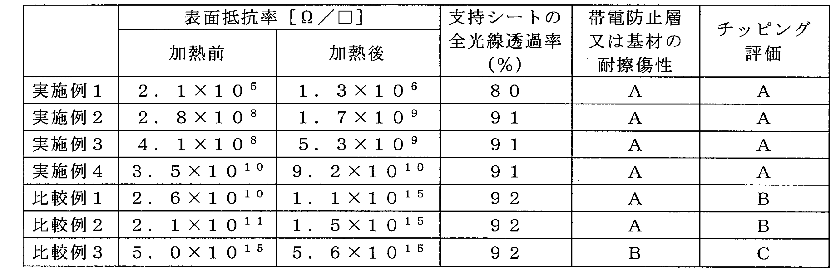
10,20,30,40,50・・・支持シート
10a,20a,30a,40a,50a・・・支持シートの第1面
11・・・基材
11a・・・基材の第1面
11b・・・基材の第2面
11’・・・帯電防止性基材
12・・・粘着剤層
13,23・・・保護膜形成用フィルム
130・・・切断後の保護膜形成用フィルム
13’・・・保護膜
130’・・・切断後の保護膜
15・・・剥離フィルム
17・・・背面帯電防止層
19・・・表面帯電防止層
9・・・半導体ウエハ
9b・・・半導体ウエハの裏面
9’・・・半導体チップ
Claims (6)
- 支持シートと、前記支持シートの一方の面上に形成された熱硬化性保護膜形成用フィルムと、を備えた、保護膜形成用複合シートであって、
前記熱硬化性保護膜形成用フィルムの加熱硬化前における、前記保護膜形成用複合シート中の、前記支持シート側の最表層の表面抵抗率が1.0×10¹¹Ω/□以下であり、
前記熱硬化性保護膜形成用フィルムの加熱硬化後における、前記保護膜形成用複合シート中の、前記支持シート側の最表層の表面抵抗率が1.0×10¹¹Ω/□以下である、保護膜形成用複合シート。 - 前記支持シートが、基材と、前記基材の片面又は両面上に形成された帯電防止層と、を備えているか、又は、
前記支持シートが、帯電防止層として、帯電防止性を有する基材を備えた、請求項1に記載の保護膜形成用複合シート。 - 前記基材の片面又は両面上に形成された帯電防止層の厚さが、100nm以下である、請求項2に記載の保護膜形成用複合シート。
- 前記支持シートの全光線透過率が80%以上である、請求項2又は3に記載の保護膜形成用複合シート。
- 面積が2cm×2cmで平面状である押圧面を有する押圧手段の前記押圧面に、フランネル布を被せ、前記フランネル布を被せた前記押圧面を、前記帯電防止層の表面に押し当て、この状態で、前記押圧手段によって125g/cm2の荷重を前記帯電防止層に加えて押圧しながら、前記押圧手段を10cmの直線距離で10回往復運動させることにより、前記帯電防止層を擦った後、前記帯電防止層のこの擦った面のうち、面積が2cm×2cmの領域を目視観察したとき、傷が認められない、請求項2~4のいずれか一項に記載の保護膜形成用複合シート。
- 請求項1~5のいずれか一項に記載の保護膜形成用複合シート中の熱硬化性保護膜形成用フィルムを、半導体ウエハに貼付する工程と、
前記半導体ウエハに貼付した後の前記熱硬化性保護膜形成用フィルムを熱硬化させて、保護膜を形成する工程と、
前記半導体ウエハを分割し、前記保護膜又は熱硬化性保護膜形成用フィルムを切断して、切断後の保護膜又は熱硬化性保護膜形成用フィルムを備えた複数個の半導体チップを得る工程と、
前記切断後の保護膜又は熱硬化性保護膜形成用フィルムを備えた半導体チップを、前記支持シートから引き離してピックアップする工程と、を有する、半導体チップの製造方法。
Priority Applications (4)
| Application Number | Priority Date | Filing Date | Title |
|---|---|---|---|
| KR1020257025994A KR20250121613A (ko) | 2018-12-05 | 2019-11-27 | 보호막 형성용 복합 시트, 및 반도체 칩의 제조 방법 |
| CN201980075529.0A CN113016066A (zh) | 2018-12-05 | 2019-11-27 | 保护膜形成用复合片及半导体芯片的制造方法 |
| KR1020217013503A KR20210100085A (ko) | 2018-12-05 | 2019-11-27 | 보호막 형성용 복합 시트, 및 반도체 칩의 제조 방법 |
| JP2020559104A JP7495355B2 (ja) | 2018-12-05 | 2019-11-27 | 保護膜形成用複合シート、及び半導体チップの製造方法 |
Applications Claiming Priority (2)
| Application Number | Priority Date | Filing Date | Title |
|---|---|---|---|
| JP2018-228528 | 2018-12-05 | ||
| JP2018228528 | 2018-12-05 |
Publications (1)
| Publication Number | Publication Date |
|---|---|
| WO2020116282A1 true WO2020116282A1 (ja) | 2020-06-11 |
Family
ID=70975070
Family Applications (1)
| Application Number | Title | Priority Date | Filing Date |
|---|---|---|---|
| PCT/JP2019/046381 Ceased WO2020116282A1 (ja) | 2018-12-05 | 2019-11-27 | 保護膜形成用複合シート、及び半導体チップの製造方法 |
Country Status (5)
| Country | Link |
|---|---|
| JP (1) | JP7495355B2 (ja) |
| KR (2) | KR20210100085A (ja) |
| CN (1) | CN113016066A (ja) |
| TW (1) | TWI822917B (ja) |
| WO (1) | WO2020116282A1 (ja) |
Cited By (1)
| Publication number | Priority date | Publication date | Assignee | Title |
|---|---|---|---|---|
| JP2022157810A (ja) * | 2021-03-31 | 2022-10-14 | リンテック株式会社 | 支持シート、樹脂膜形成用複合シート、キット、及び、樹脂膜付きチップの製造方法 |
Citations (8)
| Publication number | Priority date | Publication date | Assignee | Title |
|---|---|---|---|---|
| JPH10217379A (ja) * | 1997-02-03 | 1998-08-18 | Toyobo Co Ltd | 導電性積層フィルム |
| JP2008280520A (ja) * | 2007-04-11 | 2008-11-20 | Furukawa Electric Co Ltd:The | 半導体固定用粘着テープ |
| JP2013120839A (ja) * | 2011-12-07 | 2013-06-17 | Lintec Corp | 保護膜形成層付ダイシングシートおよびチップの製造方法 |
| JP2016096239A (ja) * | 2014-11-14 | 2016-05-26 | 住友ベークライト株式会社 | 半導体用ウエハ加工用粘着テープ |
| JP2017011057A (ja) * | 2015-06-19 | 2017-01-12 | 住友ベークライト株式会社 | 半導体用ウエハ加工用粘着テープ |
| JP2017011199A (ja) * | 2015-06-25 | 2017-01-12 | リンテック株式会社 | 保護膜形成用フィルム、保護膜形成用シート、ワーク又は加工物の製造方法、検査方法、良品と判断されたワーク、及び良品と判断された加工物 |
| JP2017119749A (ja) * | 2015-12-28 | 2017-07-06 | 日東電工株式会社 | 透明導電性フィルム用保護フィルム及び積層体 |
| WO2017188216A1 (ja) * | 2016-04-28 | 2017-11-02 | リンテック株式会社 | 保護膜形成用フィルムおよび保護膜形成用複合シート |
Family Cites Families (3)
| Publication number | Priority date | Publication date | Assignee | Title |
|---|---|---|---|---|
| JP6297786B2 (ja) | 2012-12-10 | 2018-03-20 | 日東電工株式会社 | 接着シート、ダイシングテープ一体型接着シート、半導体装置の製造方法、及び、半導体装置 |
| JP6077922B2 (ja) * | 2012-12-10 | 2017-02-08 | 日東電工株式会社 | ダイシングテープ一体型接着シート、ダイシングテープ一体型接着シートを用いた半導体装置の製造方法、及び、半導体装置 |
| SG11201610546VA (en) * | 2014-07-03 | 2018-01-30 | Lintec Corp | Composite sheet for forming protective film |
-
2019
- 2019-11-27 JP JP2020559104A patent/JP7495355B2/ja active Active
- 2019-11-27 KR KR1020217013503A patent/KR20210100085A/ko not_active Ceased
- 2019-11-27 KR KR1020257025994A patent/KR20250121613A/ko active Pending
- 2019-11-27 WO PCT/JP2019/046381 patent/WO2020116282A1/ja not_active Ceased
- 2019-11-27 CN CN201980075529.0A patent/CN113016066A/zh active Pending
- 2019-12-03 TW TW108144032A patent/TWI822917B/zh active
Patent Citations (8)
| Publication number | Priority date | Publication date | Assignee | Title |
|---|---|---|---|---|
| JPH10217379A (ja) * | 1997-02-03 | 1998-08-18 | Toyobo Co Ltd | 導電性積層フィルム |
| JP2008280520A (ja) * | 2007-04-11 | 2008-11-20 | Furukawa Electric Co Ltd:The | 半導体固定用粘着テープ |
| JP2013120839A (ja) * | 2011-12-07 | 2013-06-17 | Lintec Corp | 保護膜形成層付ダイシングシートおよびチップの製造方法 |
| JP2016096239A (ja) * | 2014-11-14 | 2016-05-26 | 住友ベークライト株式会社 | 半導体用ウエハ加工用粘着テープ |
| JP2017011057A (ja) * | 2015-06-19 | 2017-01-12 | 住友ベークライト株式会社 | 半導体用ウエハ加工用粘着テープ |
| JP2017011199A (ja) * | 2015-06-25 | 2017-01-12 | リンテック株式会社 | 保護膜形成用フィルム、保護膜形成用シート、ワーク又は加工物の製造方法、検査方法、良品と判断されたワーク、及び良品と判断された加工物 |
| JP2017119749A (ja) * | 2015-12-28 | 2017-07-06 | 日東電工株式会社 | 透明導電性フィルム用保護フィルム及び積層体 |
| WO2017188216A1 (ja) * | 2016-04-28 | 2017-11-02 | リンテック株式会社 | 保護膜形成用フィルムおよび保護膜形成用複合シート |
Cited By (2)
| Publication number | Priority date | Publication date | Assignee | Title |
|---|---|---|---|---|
| JP2022157810A (ja) * | 2021-03-31 | 2022-10-14 | リンテック株式会社 | 支持シート、樹脂膜形成用複合シート、キット、及び、樹脂膜付きチップの製造方法 |
| JP7591453B2 (ja) | 2021-03-31 | 2024-11-28 | リンテック株式会社 | 支持シート、樹脂膜形成用複合シート、キット、及び、樹脂膜付きチップの製造方法 |
Also Published As
| Publication number | Publication date |
|---|---|
| TW202039734A (zh) | 2020-11-01 |
| JP7495355B2 (ja) | 2024-06-04 |
| JPWO2020116282A1 (ja) | 2021-10-21 |
| KR20250121613A (ko) | 2025-08-12 |
| TWI822917B (zh) | 2023-11-21 |
| KR20210100085A (ko) | 2021-08-13 |
| CN113016066A (zh) | 2021-06-22 |
Similar Documents
| Publication | Publication Date | Title |
|---|---|---|
| JP7292308B2 (ja) | 保護膜形成用複合シート、及び半導体チップの製造方法 | |
| JP6847929B2 (ja) | 保護膜形成用フィルムおよび保護膜形成用複合シート | |
| JP6914698B2 (ja) | 樹脂膜形成用複合シート | |
| JPWO2019172439A1 (ja) | 保護膜形成用複合シート及び保護膜付き半導体チップの製造方法 | |
| JPWO2017145938A1 (ja) | 保護膜形成用シート、保護膜形成用シートの製造方法及び半導体装置の製造方法 | |
| JP7516255B2 (ja) | 保護膜形成用複合シート、及び半導体チップの製造方法 | |
| JP6686241B1 (ja) | 保護膜形成用フィルム、保護膜形成用複合シート、検査方法及び識別方法 | |
| JP7495355B2 (ja) | 保護膜形成用複合シート、及び半導体チップの製造方法 | |
| JP7516256B2 (ja) | 保護膜形成用複合シート、及び半導体チップの製造方法 | |
| JP7497297B2 (ja) | 保護膜形成用複合シート、及び半導体チップの製造方法 | |
| JP7482035B2 (ja) | 保護膜形成用複合シート、及び半導体チップの製造方法 |
Legal Events
| Date | Code | Title | Description |
|---|---|---|---|
| 121 | Ep: the epo has been informed by wipo that ep was designated in this application |
Ref document number: 19892381 Country of ref document: EP Kind code of ref document: A1 |
|
| ENP | Entry into the national phase |
Ref document number: 2020559104 Country of ref document: JP Kind code of ref document: A |
|
| NENP | Non-entry into the national phase |
Ref country code: DE |
|
| 122 | Ep: pct application non-entry in european phase |
Ref document number: 19892381 Country of ref document: EP Kind code of ref document: A1 |
|
| WWR | Wipo information: refused in national office |
Ref document number: 1020217013503 Country of ref document: KR |
|
| WWC | Wipo information: continuation of processing after refusal or withdrawal |
Ref document number: 1020217013503 Country of ref document: KR |
|
| WWR | Wipo information: refused in national office |
Ref document number: 1020217013503 Country of ref document: KR |
|
| WWD | Wipo information: divisional of initial pct application |
Ref document number: 1020257025994 Country of ref document: KR |
|
| WWP | Wipo information: published in national office |
Ref document number: 1020257025994 Country of ref document: KR |