WO2020116147A1 - 電界効果トランジスタおよびその製造方法 - Google Patents
電界効果トランジスタおよびその製造方法 Download PDFInfo
- Publication number
- WO2020116147A1 WO2020116147A1 PCT/JP2019/045211 JP2019045211W WO2020116147A1 WO 2020116147 A1 WO2020116147 A1 WO 2020116147A1 JP 2019045211 W JP2019045211 W JP 2019045211W WO 2020116147 A1 WO2020116147 A1 WO 2020116147A1
- Authority
- WO
- WIPO (PCT)
- Prior art keywords
- layer
- effect transistor
- channel
- inp
- mesa
- Prior art date
- Legal status (The legal status is an assumption and is not a legal conclusion. Google has not performed a legal analysis and makes no representation as to the accuracy of the status listed.)
- Ceased
Links
Images





Classifications
-
- H—ELECTRICITY
- H10—SEMICONDUCTOR DEVICES; ELECTRIC SOLID-STATE DEVICES NOT OTHERWISE PROVIDED FOR
- H10D—INORGANIC ELECTRIC SEMICONDUCTOR DEVICES
- H10D30/00—Field-effect transistors [FET]
- H10D30/40—FETs having zero-dimensional [0D], one-dimensional [1D] or two-dimensional [2D] charge carrier gas channels
- H10D30/47—FETs having zero-dimensional [0D], one-dimensional [1D] or two-dimensional [2D] charge carrier gas channels having two-dimensional [2D] charge carrier gas channels, e.g. nanoribbon FETs or high electron mobility transistors [HEMT]
- H10D30/471—High electron mobility transistors [HEMT] or high hole mobility transistors [HHMT]
- H10D30/473—High electron mobility transistors [HEMT] or high hole mobility transistors [HHMT] having confinement of carriers by multiple heterojunctions, e.g. quantum well HEMT
- H10D30/4732—High electron mobility transistors [HEMT] or high hole mobility transistors [HHMT] having confinement of carriers by multiple heterojunctions, e.g. quantum well HEMT using Group III-V semiconductor material
-
- H—ELECTRICITY
- H10—SEMICONDUCTOR DEVICES; ELECTRIC SOLID-STATE DEVICES NOT OTHERWISE PROVIDED FOR
- H10D—INORGANIC ELECTRIC SEMICONDUCTOR DEVICES
- H10D30/00—Field-effect transistors [FET]
- H10D30/40—FETs having zero-dimensional [0D], one-dimensional [1D] or two-dimensional [2D] charge carrier gas channels
- H10D30/47—FETs having zero-dimensional [0D], one-dimensional [1D] or two-dimensional [2D] charge carrier gas channels having two-dimensional [2D] charge carrier gas channels, e.g. nanoribbon FETs or high electron mobility transistors [HEMT]
- H10D30/471—High electron mobility transistors [HEMT] or high hole mobility transistors [HHMT]
- H10D30/475—High electron mobility transistors [HEMT] or high hole mobility transistors [HHMT] having wider bandgap layer formed on top of lower bandgap active layer, e.g. undoped barrier HEMTs such as i-AlGaN/GaN HEMTs
-
- H—ELECTRICITY
- H10—SEMICONDUCTOR DEVICES; ELECTRIC SOLID-STATE DEVICES NOT OTHERWISE PROVIDED FOR
- H10D—INORGANIC ELECTRIC SEMICONDUCTOR DEVICES
- H10D30/00—Field-effect transistors [FET]
- H10D30/01—Manufacture or treatment
- H10D30/015—Manufacture or treatment of FETs having heterojunction interface channels or heterojunction gate electrodes, e.g. HEMT
-
- H—ELECTRICITY
- H10—SEMICONDUCTOR DEVICES; ELECTRIC SOLID-STATE DEVICES NOT OTHERWISE PROVIDED FOR
- H10D—INORGANIC ELECTRIC SEMICONDUCTOR DEVICES
- H10D30/00—Field-effect transistors [FET]
- H10D30/80—FETs having rectifying junction gate electrodes
- H10D30/87—FETs having Schottky gate electrodes, e.g. metal-semiconductor FETs [MESFET]
-
- H—ELECTRICITY
- H10—SEMICONDUCTOR DEVICES; ELECTRIC SOLID-STATE DEVICES NOT OTHERWISE PROVIDED FOR
- H10D—INORGANIC ELECTRIC SEMICONDUCTOR DEVICES
- H10D62/00—Semiconductor bodies, or regions thereof, of devices having potential barriers
- H10D62/10—Shapes, relative sizes or dispositions of the regions of the semiconductor bodies; Shapes of the semiconductor bodies
- H10D62/13—Semiconductor regions connected to electrodes carrying current to be rectified, amplified or switched, e.g. source or drain regions
- H10D62/149—Source or drain regions of field-effect devices
-
- H—ELECTRICITY
- H10—SEMICONDUCTOR DEVICES; ELECTRIC SOLID-STATE DEVICES NOT OTHERWISE PROVIDED FOR
- H10D—INORGANIC ELECTRIC SEMICONDUCTOR DEVICES
- H10D62/00—Semiconductor bodies, or regions thereof, of devices having potential barriers
- H10D62/10—Shapes, relative sizes or dispositions of the regions of the semiconductor bodies; Shapes of the semiconductor bodies
- H10D62/13—Semiconductor regions connected to electrodes carrying current to be rectified, amplified or switched, e.g. source or drain regions
- H10D62/149—Source or drain regions of field-effect devices
- H10D62/151—Source or drain regions of field-effect devices of IGFETs
-
- H—ELECTRICITY
- H10—SEMICONDUCTOR DEVICES; ELECTRIC SOLID-STATE DEVICES NOT OTHERWISE PROVIDED FOR
- H10D—INORGANIC ELECTRIC SEMICONDUCTOR DEVICES
- H10D62/00—Semiconductor bodies, or regions thereof, of devices having potential barriers
- H10D62/80—Semiconductor bodies, or regions thereof, of devices having potential barriers characterised by the materials
- H10D62/82—Heterojunctions
- H10D62/824—Heterojunctions comprising only Group III-V materials heterojunctions, e.g. GaN/AlGaN heterojunctions
-
- H—ELECTRICITY
- H10—SEMICONDUCTOR DEVICES; ELECTRIC SOLID-STATE DEVICES NOT OTHERWISE PROVIDED FOR
- H10D—INORGANIC ELECTRIC SEMICONDUCTOR DEVICES
- H10D84/00—Integrated devices formed in or on semiconductor substrates that comprise only semiconducting layers, e.g. on Si wafers or on GaAs-on-Si wafers
- H10D84/101—Integrated devices comprising main components and built-in components, e.g. IGBT having built-in freewheel diode
- H10D84/141—VDMOS having built-in components
- H10D84/146—VDMOS having built-in components the built-in components being Schottky barrier diodes
-
- H—ELECTRICITY
- H10—SEMICONDUCTOR DEVICES; ELECTRIC SOLID-STATE DEVICES NOT OTHERWISE PROVIDED FOR
- H10D—INORGANIC ELECTRIC SEMICONDUCTOR DEVICES
- H10D30/00—Field-effect transistors [FET]
- H10D30/01—Manufacture or treatment
- H10D30/021—Manufacture or treatment of FETs having insulated gates [IGFET]
-
- H—ELECTRICITY
- H10—SEMICONDUCTOR DEVICES; ELECTRIC SOLID-STATE DEVICES NOT OTHERWISE PROVIDED FOR
- H10D—INORGANIC ELECTRIC SEMICONDUCTOR DEVICES
- H10D30/00—Field-effect transistors [FET]
- H10D30/60—Insulated-gate field-effect transistors [IGFET]
-
- H—ELECTRICITY
- H10—SEMICONDUCTOR DEVICES; ELECTRIC SOLID-STATE DEVICES NOT OTHERWISE PROVIDED FOR
- H10D—INORGANIC ELECTRIC SEMICONDUCTOR DEVICES
- H10D62/00—Semiconductor bodies, or regions thereof, of devices having potential barriers
- H10D62/80—Semiconductor bodies, or regions thereof, of devices having potential barriers characterised by the materials
- H10D62/85—Semiconductor bodies, or regions thereof, of devices having potential barriers characterised by the materials being Group III-V materials, e.g. GaAs
- H10D62/852—Semiconductor bodies, or regions thereof, of devices having potential barriers characterised by the materials being Group III-V materials, e.g. GaAs being Group III-V materials comprising three or more elements, e.g. AlGaN or InAsSbP
Definitions
- the present invention relates to a field effect transistor and a method for manufacturing the same.
- An InP-based heterostructure field effect transistor using a III-V group compound semiconductor grown on a semi-insulating InP substrate is an InP-based high electron mobility transistor (InP-based high electron mobility transistor). It is also called electron mobility transistor (hereinafter, InP HEMT). Since these transistors use a channel made of InGaAs or InAs having high electron mobility, they have excellent high-speed performance and low noise characteristics, and as described in Non-Patent Documents 1 and 2, the sub-terahertz and terahertz bands. It is expected to be applied to the ultra-high frequency integrated circuit that operates at.
- MOSFET metal-oxide-semiconductor field effect transistor having a channel of a III-V group compound semiconductor such as InGaAs or InAs.
- III-V-MOSFET a metal-oxide-semiconductor field effect transistor having a channel of a III-V group compound semiconductor such as InGaAs or InAs.
- MOSFET metal-oxide-semiconductor field effect transistor
- MOVPE metal-organic vapor phase epitaxy
- MOCVD metal-organic chemical vapor deposition
- InP-based HEMTs and InP-based III-V-MOSFETs it is important to reduce the access resistance between the source electrode and the channel and between the channel and the drain electrode in order to improve the transistor performance.
- a source electrode and a drain electrode are formed on a contact layer made of n-type InGaAs or n-type InAlAs, and an access resistance between the channel and We are trying to reduce it.
- the undoped InAlAs or InP layer that acts as a spacer or a barrier layer under the gate electrode is sandwiched between the n-type contact layer and the channel layer, and only the portion passing through these layers is accessed.
- the resistance increases.
- the spacer layer and the barrier layer in the region under the source electrode and the drain electrode are removed, and Si is heavily doped on the buffer layer.
- a technique has been reported in which the access resistance is reduced by re-growing the above-mentioned InGaAs by an epitaxial growth method.
- Non-Patent Document 6 Also in the production of an InP-based MOSFET formed on an InP substrate, as described in Non-Patent Document 6, a semiconductor layer which is heavily doped by the above-described regrowth method is formed in the region under the source and drain electrodes. Technology has been reported.
- wet etching is mainly used to remove the layers that are not necessary for forming the highly-doped contact layer described above. This is because it is difficult for the dry etching method to flatten the surface after etching at the atomic level. In order to form a high quality contact layer by regrowth, it is desirable that the surface exposed by etching has atomic level flatness. However, the flatness of the exposed surface cannot be ensured by dry etching, which is not preferable for forming a high quality contact layer by regrowth.
- a method of inserting an InP layer having a high etching selectivity for InGaAs or InAlAs as an etching stop layer in order to control the etching depth with high precision and to form a flat surface after etching there is.
- this layer structure it is possible to automatically stop the etching at the InP layer and selectively remove the InGaAs channel layer by wet etching.
- the surface of the exposed InP layer can be flattened at the atomic level because it is processed by wet etching.
- the conduction band discontinuity between the InGaAs channel layer and the InP layer is smaller than the band discontinuity between the InGaAs channel layer and the InAlAs buffer layer. Therefore, in the case of manufacturing by the method described above, there is a problem that the electron confinement in the InGaAs channel layer becomes insufficient, the InP layer also acts as a channel, and the electron mobility decreases. Further, since the electron confinement in the InGaAs channel layer is weakened, the short channel effect is more likely to occur in a device having a short gate length as compared with the structure in which the InGaAs channel is directly laminated on the InAlAs buffer layer.
- the present invention has been made in order to solve the above-mentioned problems, and in the state in which the decrease in electron mobility in the channel layer and the short channel effect are suppressed, the source/drain electrode and the channel layer are provided.
- the purpose is to reduce the access resistance more easily.
- a buffer layer made of a compound semiconductor lattice-matching with InP and a thickness made of In x Al 1-x P (0 ⁇ x ⁇ 0.75) are formed on a substrate.
- a third step of forming the first contact layer and the second contact layer a fourth step of forming a gate electrode on the channel layer of the mesa, a source electrode on the first contact layer, and a second contact
- a fifth step of forming a drain electrode on the layer A third step of forming the first contact layer and the second contact layer, a fourth step of forming a gate electrode on the channel layer of the mesa, a source electrode on the first contact layer, and a second contact.
- a buffer layer, an etching stopper layer, a channel layer, an electron supply layer made of a compound semiconductor, a barrier layer made of InAlAs, and a cap layer made of InP are used.
- the cap layer, the barrier layer, the electron supply layer, and the channel layer are patterned to form a mesa, and in the fourth step, a gate electrode is formed on the cap layer of the mesa.
- the substrate is made of semi-insulating InP.
- the substrate is made of Si
- the buffer layer is made of GaAs or InP.
- the substrate is made of GaAs
- the buffer layer is made of InP.
- a field effect transistor includes a buffer layer formed on a substrate and made of a compound semiconductor lattice-matched to InP, and In x Al 1-x P (0 ⁇ x ⁇ 0.75) and a channel layer made of In y Ga 1-y As (0 ⁇ y ⁇ 1) formed on the etching stop layer and having a thickness not more than the critical film thickness.
- Mesa, the first contact layer and the second contact layer of In z Ga 1-z As (0 ⁇ z ⁇ 1) formed on the etching stop layers on both sides of the mesa, and the channel of the mesa A gate electrode formed on the layer, a source electrode formed on the first contact layer, and a drain electrode formed on the second contact layer.
- the mesa includes an electron supply layer made of a compound semiconductor formed on the channel layer, a barrier layer made of InAlAs formed on the electron supply layer, and a barrier layer formed on the barrier layer. And a cap layer made of InP, the gate electrode being formed on the cap layer.
- the etching stop layer under the channel layer made of In y Ga 1-y As (0 ⁇ y ⁇ 1) is formed as In x Al 1-x P (0 ⁇ x ⁇ 1). 0.75), it is possible to more easily reduce the access resistance between the source/drain electrode and the channel layer while suppressing the decrease in electron mobility and the short channel effect in the channel layer. That is an excellent effect.
- FIG. 1A is a cross-sectional view showing a configuration of a field effect transistor in an intermediate step for explaining a method for manufacturing a field effect transistor according to an embodiment of the present invention.
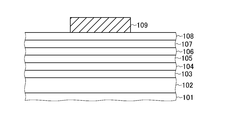
- FIG. 1B is a cross-sectional view showing the structure of the field-effect transistor in the middle of the process for explaining the method for manufacturing the field-effect transistor according to the embodiment of the present invention.
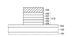
- FIG. 1C is a cross-sectional view showing the structure of the field-effect transistor in the middle of the process for explaining the method for manufacturing the field-effect transistor according to the embodiment of the present invention.
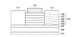
- FIG. 1D is a cross-sectional view showing the structure of the field-effect transistor in the middle of the process for explaining the method for manufacturing the field-effect transistor according to the embodiment of the present invention.
- FIG. 1A is a cross-sectional view showing a configuration of a field effect transistor in an intermediate step for explaining a method for manufacturing a field effect transistor according to an embodiment of the present invention.
- FIG. 1B is a cross-
- FIG. 1E is a cross-sectional view showing the structure of the field-effect transistor in the middle of the process for explaining the method for manufacturing the field-effect transistor according to the embodiment of the present invention.
- FIG. 1F is a cross-sectional view showing the structure of the field-effect transistor in the middle of the process for explaining the method for manufacturing the field-effect transistor according to the embodiment of the present invention.
- FIG. 1G is a cross-sectional view showing the structure of the field-effect transistor in the middle of the process for explaining the method for manufacturing the field-effect transistor according to the embodiment of the present invention.
- FIG. 2 is a sectional view showing the configuration of another field effect transistor according to the embodiment of the present invention.
- FIG. 3 is a cross-sectional view showing the configuration of another field effect transistor according to the embodiment of the present invention.
- FIGS. 1A to 1G a method for manufacturing the field effect transistor according to the embodiment of the present invention will be described with reference to FIGS. 1A to 1G.
- a buffer layer 102, an etching stop layer 103, and a channel layer 104 are epitaxially grown in this order on a substrate 101 (first step).
- a spacer layer 105, an electron supply layer 106, a barrier layer 107, and a cap layer 108 are further formed on the channel layer 104.
- the buffer layer 102, the etching stop layer 103, the channel layer 104, the spacer layer 105, the electron supply layer 106, the barrier layer 107, and the cap layer 108 are formed in this order on the substrate 101 by an epitaxial crystal such as an MBE method or a MOVPE method. It is formed by epitaxial growth using a growth method.
- the substrate 101 is made of, for example, InP having a high resistance by doping Fe.
- the buffer layer 102 is composed of a compound semiconductor that lattice-matches with InP.
- the buffer layer 102 is formed to have a thickness of about 200 nm.
- the etching stop layer 103 is composed of In x Al 1-x P (0 ⁇ x ⁇ 0.75).
- the thickness of the etching stop layer 103 is set to be equal to or less than the critical film thickness at which misfit dislocations due to lattice mismatch do not occur.
- lattice mismatch a state in which the lattice constants of the surface of the substrate 101 in the plane direction do not match.
- the channel layer 104 is composed of In y Ga 1-y As (0 ⁇ y ⁇ 1). More preferably, in the channel layer 104, the In composition y of In y Ga 1-y As is larger than 0.53 which is lattice-matched to InP. Further, the thickness of the channel layer 104 is set to be equal to or less than the critical thickness of InGaAs that does not cause misfit dislocation due to lattice mismatch. For example, the channel layer 104 has a thickness of about 10 nm.
- the spacer layer 105 is composed of InAlAs.
- the spacer layer 105 is formed to have a thickness of about 3 nm, for example.
- the electron supply layer 106 is composed of a compound semiconductor such as InAlAs.
- the electron supply layer 106 is doped with Si.
- the electron supply layer 106 is planarly doped with Si, and the Si sheet concentration is, for example, about 5 ⁇ 10 12 cm ⁇ 2 .
- the concentration of Si in the electron supply layer 106 is appropriately adjusted to obtain a desired threshold voltage in HEMT.
- the barrier layer 107 is composed of, for example, InAlAs.
- the barrier layer 107 is formed to have a thickness of about 6 nm.
- the cap layer 108 is made of InP.
- the cap layer 108 is formed to have a thickness of about 5 nm.
- the etching stop layer 103 made of In x Al 1-x P (0 ⁇ x ⁇ 0.75) is the channel layer 104 made of In y Ga 1-y As (0 ⁇ y ⁇ 1).
- the band discontinuity between and is larger than that when the etching stop layer is made of InAlAs.
- an inorganic mask pattern 109 is formed in the region where the gate electrode is formed.
- the inorganic mask pattern 109 can be made of, for example, silicon oxide (SiO 2 ).
- the shape of the inorganic mask pattern 109 in a plan view is, for example, a stripe shape extending to the back (gate width direction) from the front side of the paper surface of FIG. 1B.
- a mask layer having an opening at a position where the inorganic mask pattern 109 is formed is formed on the cap layer 108 by a known lithography technique.
- silicon oxide is deposited on the mask layer by a well-known chemical vapor deposition method or the like. By this treatment, silicon oxide is also deposited inside the opening of the mask layer. After that, the mask layer is removed (lifted off) to remove the silicon oxide on the mask layer and leave the silicon oxide deposited on the opening of the mask layer.
- the pattern 109 can be formed.
- the channel layer 104 is patterned using the inorganic mask pattern 109 as a mask by an etching process in which the etching is stopped at the etching stop layer 103 to form a mesa 110 made of the channel layer 104 as shown in FIG. 1C (second). Process). More specifically, the channel layer 104 in the region where the inorganic mask pattern 109 is not formed is etched and removed by the wet etching process in which the channel layer 104 is etched but the etching stopper layer 103 is not etched to form the mesa 110.
- the shape of the mesa 110 in a plan view is, for example, formed in a stripe shape extending to the back (gate width direction) from the front of the paper surface of FIG. 1C.
- the channel layer 104 is used in the etching process using the inorganic mask pattern 109 as a mask.
- the spacer layer 105, the electron supply layer 106, the barrier layer 107, and the cap layer 108 are patterned to form a mesa 110 including the channel layer 104, the spacer layer 105, the electron supply layer 106, the barrier layer 107, and the cap layer 108.
- the cap layer 108 made of InP, the barrier layer 107 made of InAlAs, the electron supply layer 106, and the spacer layer 105 can be etched.
- the channel layer 104 made of InGaAs is hardly etched.
- the channel layer 104 made of InGaAs can be etched.
- the etching stopper layer 103 made of In x Al 1-x P is not etched, and the surface of the etching stopper layer 103 which is flat at the atomic level can be exposed on both sides of the mesa 110.
- In z Ga 1-z As (0 ⁇ z ⁇ 1) having a relatively high concentration of n-type impurity introduced is regrown, and as shown in FIG. 1D.
- the first contact layer 111 and the second contact layer 112 are formed (third step).
- In z Ga 1-z As (0 ⁇ z ⁇ 1) having an n-type impurity introduced therein can be regrown by an epitaxial growth method such as MBE method or MOVPE method.
- the inorganic mask pattern 109 is used as a selective growth mask, and the growth conditions are set so that In z Ga 1-z As (0 ⁇ z ⁇ 1) is not deposited on the silicon oxide.
- the doping concentration of the n-type impurity is, for example, 5 ⁇ 10 19 cm ⁇ 3 or more (see Non-Patent Documents 6 and 7).
- the inorganic mask pattern 109 is removed, and the uppermost layer (cap layer 108) of the mesa 110 is exposed as shown in FIG. 1E.
- the inorganic mask pattern 109 made of silicon oxide can be selectively removed by wet etching using an HF-based etchant.
- the gate electrode 121 is formed on the channel layer 104 of the mesa 110 (fourth step).
- the spacer layer 105, the electron supply layer 106, the barrier layer 107, and the cap layer 108 are formed on the channel layer 104, and the Schottky-connected gate electrode 121 is formed on the cap layer 108.
- the well-known lift-off method can be used to form the gate electrode 121 from a predetermined gate electrode material.
- the source electrode 122 is formed on the first contact layer 111, and the drain electrode 123 is formed on the second contact layer 112 (fifth step).
- the source electrode 122 is formed so as to be in ohmic contact with the first contact layer 111.
- the drain electrode 123 is formed in a state of being in ohmic contact with the second contact layer 112.
- the well-known lift-off method can form the source electrode 122 and the drain electrode 123 from a predetermined electrode material.
- a field effect transistor including the gate electrode 121 formed on the first contact layer 111, the source electrode 122 formed on the first contact layer 111, and the drain electrode 123 formed on the second contact layer 112 is obtained.
- the mesa 110 includes the spacer layer 105 formed on the channel layer 104, the electron supply layer 106 formed on the spacer layer 105, and the barrier layer formed on the electron supply layer 106. 107 and a cap layer 108 formed on the barrier layer 107, and the gate electrode 121 is formed on the cap layer 108.
- the manufacturing method of the above-described embodiment it is possible to form the first contact layer 111 and the second contact layer 112 of high quality by epitaxial growth from the surface of the etching stopper layer 103 which is flat at the atomic level. .. As a result, a field effect transistor having low access resistance between the source/drain electrodes and the channel layer can be manufactured.
- the channel layer 104 since the etching stop layer 103 disposed under the channel layer 104 composed of In y Ga 1-y As is composed of In x Al 1-x P (0 ⁇ x ⁇ 0.75), the channel layer 104 The conduction band discontinuity between the etching stopper layer 103 and the etching stop layer 103 becomes larger than that of InGaAs/InAlAs. Thereby, the confinement of electrons inside the channel layer 104 is promoted, and the short channel effect in the field effect transistor can be suppressed.
- the channel layer 104 is composed of one layer in the above description, as shown in FIG. 2, it may have a three-layer structure of the first channel layer 104a, the second channel layer 104b, and the third channel layer 104c.
- the first channel layer 104a, the second channel layer 104b, the third channel layer 104c, the spacer layer 105, the electron supply layer 106, the barrier layer 107, and the cap layer 108 form the mesa 110a.
- the first channel layer 104a and the third channel layer 104c are made of InGaAs having an In composition x satisfying 0.53 ⁇ x ⁇ 0.8, and the second channel layer 104b is made of InGaAs satisfying 0.8 ⁇ x ⁇ 1. It consists of. With this structure, the band gap of the conduction band edge of the second channel layer 104b is lower than that of the first channel layer 104a and the third channel layer 104c.
- the second channel layer 104b has a thickness less than a so-called critical thickness at which misfit dislocations due to lattice mismatch between upper and lower layers do not occur.
- the gate electrode 121 may be formed on the cap layer 108 via the gate insulating layer 113, as shown in FIG.
- the gate insulating layer 113 can be made of, for example, an oxide such as Al 2 O 3 or HfO 2 .
- the HEMT has been described as an example, but the same applies to the case of the MOSFET.
- the substrate is not limited to InP, but may be made of Si, GaAs, or the like (see Non-Patent Document 7).
- a crystal layer having the same lattice constant as that of InP grown through an intentionally relaxed buffer layer is formed on a substrate composed of Si or GaAs, and the buffer layer and the etching are formed on the crystal layer. It is also possible to epitaxially grow the stop layer and the channel layer.
- the first contact layer and the second contact layer are not limited to those composed of InGaAs having a uniform composition in the layer thickness direction.
- the etching stop layer side may be made of InGaAs lattice-matched to InP, and the source electrode and drain electrode sides may be made of InGaAs or InAs having a high In composition.
- the region composed of InGaAs or InAs having a high In composition is set to have a critical film thickness or less at which misfit dislocations do not occur.
- the inorganic mask pattern was removed after the first contact layer and the second contact layer were regrown using the inorganic mask pattern, and the gate electrode was formed after this, but the present invention is not limited to this.
- the etching stopper layer is exposed by etching using the gate electrode as a mask, and the exposed contact layer is used to form the first contact.
- the layer, the second contact layer can also be regrown.
- a cap layer may be formed on a channel layer, and a gate electrode may be formed on the cap layer via a gate insulating layer.
- the etching stop layer below the channel layer made of In y Ga 1-y As (0 ⁇ y ⁇ 1) is formed as In x Al 1-x P (0 ⁇ x ⁇ 0.75), it is possible to more easily reduce the access resistance between the source/drain electrode and the channel layer while suppressing the decrease in electron mobility and the short channel effect in the channel layer. become able to.
- Substrate 102... Buffer layer, 103... Etch stop layer, 104... Channel layer, 105... Spacer layer, 106... Electron supply layer, 107... Barrier layer, 108... Cap layer, 109... Inorganic mask pattern, 110... Mesa , 111... First contact layer, 112... Second contact layer, 121... Gate electrode, 122... Source electrode, 123... Drain electrode.
Landscapes
- Junction Field-Effect Transistors (AREA)
- Insulated Gate Type Field-Effect Transistor (AREA)
Abstract
基板(101)の上に、バッファ層(102)、エッチング停止層(103)、チャネル層(104)を、これらの順にエピタキシャル成長する。基板(101)は、例えば、Feをドープすることで高抵抗としたInPから構成する。バッファ層(102)は、InPに格子整合する化合物半導体から構成する。エッチング停止層(103)は、InxAl1-xP(0≦x≦0.75)から構成する。チャネル層(104)は、InyGa1-yAs(0<y≦1)から構成する。
Description
本発明は、電界効果トランジスタおよびその製造方法に関する。
半絶縁性InP基板の上に成長したIII-V族化合物半導体を用いたInP系ヘテロ接合型電界効果トランジスタ(InP-based heterostructure field effect transistor)は、InP系高電子移動度トランジスタ(InP-based high electron mobility transistor、以下、InP系HEMT)とも呼ばれている。これらのトランジスタは、高い電子移動度を有するInGaAsやInAsからなるチャネルを用いることから、優れた高速性および低雑音性を有し、非特許文献1および2に記載のようにサブテラヘルツおよびテラヘルツ帯で動作する超高周波集積回路への応用が期待されている。
また、InGaAsやInAsなどのIII-V族化合物半導体をチャネルとする金属-酸化物-半導体電界効果トランジスタ(metal-oxide-semiconductor field effect transistor、以下MOSFET)は、III-V-MOSFETと呼ばれ、非特許文献3に記載のように、低消費電力動作可能な次世代素子として期待されている。
これらのトランジスタは、分子線エピタキシー(Molecular Beam Epitaxy:MBE)法や、有機金属気相成長(Metal-Organic Vapor-Phase Epitaxy:MOVPE、あるいはMetal-Organic Chemical Vapor Deposition:MOCVD、以下、MOVPE)法のようなエピタキシャル結晶成長法を用いて作製された薄膜(半導体層)を加工して作製される。
InP系HEMTやInP系III-V-MOSFETにおいては、ソース電極-チャネル間、およびチャネル-ドレイン電極間のアクセス抵抗を低減することが、トランジスタの性能向上において重要となる。例えば、InP系HEMTでは、非特許文献4に記載の通り、n型のInGaAsやn型のInAlAsからなるコンタクト層の上に、ソース電極、ドレイン電極を形成し、チャネルとの間のアクセス抵抗の低減を図っている。
上述した構成では、n型コンタクト層とチャネル層の間に、ゲート電極下でスペーサや障壁層として作用するドーピングを施さないInAlAsやInPの層を挟んでおり、これらの層を通過する分だけアクセス抵抗は高くなる。
このため、アクセス抵抗低減の方法として、例えば非特許文献5に記載のように、ソース電極下およびドレイン電極下となる領域のスペーサ層、障壁層を除去し、バッファ層上にSiを高濃度ドープしたInGaAsをエピタキシャル成長法により再成長し、アクセス抵抗を低減する技術が報告されている。
InP基板上に形成するInP系MOSFET作製においても、非特許文献6に記載のように、ソース、ドレイン電極下の領域には、上述した再成長法によって高濃度ドーピングを施した半導体層を形成する技術が報告されている。
上述した高濃度ドープコンタクト層形成のために不要となる層の除去は、主にウエットエッチングによって行われる。これは、ドライエッチング法では、エッチング後の表面を、原子レベルで平坦にするのは困難なためである。再成長によって高品質のコンタクト層を形成するために、エッチングによって露出させた表面は、原子レベルの平坦性を有するが望ましい。しかしながら、ドライエッチングでは露出させた表面の平坦性が確保できず、再成長によって、高品質なコンタクト層を形成するのに好ましくない。
また、チャネル層に高濃度ドープコンタクト層を直接接触させるためには、少なくともチャネル層まで、あるいはチャネル層とバッファ層とのヘテロ界面までエッチングを行う必要がある。このエッチング処理において、チャネル層を構成するInGaAsやInAsと、バリア層、スペーサ層、バッファ層を構成するInAlAsとでは、選択的なエッチングを行うことが難しいため、再現性良く所望の深さでエッチングを停止させることが困難である。
H. Hamada et al., "300-GHz, 100-Gb/s InP-HEMT Wireless Transceiver Using a 300-GHz Fundamental Mixer", IEEE/MTT-S International Microwave Symposium, 10.1109/MWSYM.2018.8439850, pp. 1480-1483, 2018.
X. Mei et al., "First Demonstration of Amplification at 1 THz Using 25-nm InP High Electron Mobility Transistor Process", IEEE Electron Device Letters, vol. 36, no. 4, pp. 327-329, 2015.
J. A. del Alamo, "Nanometre-scale electronics with III-V compound semiconductors", Nature, vol. 479, pp. 317-323, 2011.
T. Suemitsu et al., "30-nm Two-Step Recess Gate InP-Based InAlAs/InGaAs HEMTs", IEEE Transactions on Electron Devices, vol. 49, no. 10, pp. 1694-1700, 2002.
Q. Li et al., "InP Lattice-matched HEMT with Regrown Source/Drain by MOCVD", IPRM 2011 - 23rd International Conference on Indium Phosphide and Related Materials, 2011.
R. Terao et al., "InP/InGaAs Composite Metal-.Oxide-.Semiconductor Field-Effect Transistors with Regrown Source and Al2O3 Gate Dielectric Exhibiting Maximum Drain Current Exceeding 1.3 mA/μm", Applied Physics Express, vol. 4, 054201, 2011.
Q. Li et al., "Material and Device Characteristics of Metamorphic In0.53Ga0.47As MOSHEMTs Grown on GaAs and Si Substrates by MOCVD", IEEE Transactions on Electron Devices, vol. 60, no. 12, pp. 4112-4118, 2013.
上述したエッチング処理の工程において、エッチング深さの高精度制御と、エッチング後に平坦な表面を形成するために、InGaAsやInAlAsに対してエッチング選択性の高いInPの層をエッチング停止層として挿入する方法がある。例えば、InGaAsチャネル層とInAlAsバッファ層の間にInP層を挿入することが考えられる。この層構成とすれば、ウエットエッチングによって、InP層でエッチングを自動的に停止させ、選択的にInGaAsチャネル層までを除去することが可能である。また、この方法では、ウエットエッチングで処理するため、露出させたInP層の表面を、原子レベルで平坦なにすることも可能である。
しかし、InGaAsチャネル層とInP層との間の伝導帯バンド不連続が、InGaAsチャネル層とInAlAsバッファ層とのバンド不連続よりも小さい。このため、上述した方法で作製した場合、InGaAsチャネル層への電子の閉じ込めが不十分となり、InP層もチャネルとして作用し、電子移動度が低下するという問題がある。また、InGaAsチャネル層内への電子閉じ込めが弱くなることから、InAlAsバッファ層上に直接InGaAsチャネルを積層した構造と比べて、ゲート長の短い素子において短チャネル効果が生じやすくなる。
以上に説明したように、従来では、チャネル層における電子移動度の低下および短チャネル効果を抑制した状態で、ソース・ドレイン電極とチャネル層との間のアクセス抵抗を低減することが容易ではないという問題があった。
本発明は、以上のような問題点を解消するためになされたものであり、チャネル層における電子移動度の低下および短チャネル効果を抑制した状態で、ソース・ドレイン電極とチャネル層との間のアクセス抵抗を、より容易に低減することを目的とする。
本発明に係る電界効果トランジスタの製造方法は、基板の上に、InPに格子整合する化合物半導体からなるバッファ層、InxAl1-xP(0≦x≦0.75)からなる厚さが臨界膜厚以下のエッチング停止層、InyGa1-yAs(0<y≦1)からなるチャネル層を、これらの順にエピタキシャル成長する第1工程と、エッチング停止層でエッチングが停止するエッチング処理により、チャネル層をパターニングしてチャネル層からなるメサを形成する第2工程と、メサの両脇のエッチング停止層の上にInzGa1-zAs(0<z≦1)を再成長させて第1コンタクト層および第2コンタクト層を形成する第3工程と、メサのチャネル層の上にゲート電極を形成する第4工程と、第1コンタクト層の上にソース電極を形成し、第2コンタクト層の上にドレイン電極を形成する第5工程とを備える。
上記電界効果トランジスタの製造方法の一構成例において、第1工程は、バッファ層、エッチング停止層、チャネル層、化合物半導体からなる電子供給層、InAlAsからなる障壁層、InPからなるキャップ層を、これらの順にエピタキシャル成長し、第2工程は、キャップ層、障壁層、電子供給層、チャネル層をパターニングしてメサを形成し、第4工程は、メサのキャップ層の上にゲート電極を形成する。
上記電界効果トランジスタの製造方法の一構成例において、基板は、半絶縁性のInPから構成されている。
上記電界効果トランジスタの製造方法の一構成例において、基板は、Siから構成され、バッファ層は、GaAsまたはInPから構成されている。
上記電界効果トランジスタの製造方法の一構成例において、基板は、GaAsから構成され、バッファ層は、InPから構成されている。
本発明に係る電界効果トランジスタは、基板の上に形成された、InPに格子整合する化合物半導体からなるバッファ層と、バッファ層の上に形成された、InxAl1-xP(0≦x≦0.75)からなる厚さが臨界膜厚以下のエッチング停止層と、エッチング停止層の上に形成された、InyGa1-yAs(0<y≦1)からなるチャネル層から構成されたメサと、メサの両脇のエッチング停止層の上に形成された、InzGa1-zAs(0<z≦1)からなる第1コンタクト層および第2コンタクト層と、メサのチャネル層の上に形成されたゲート電極と、第1コンタクト層の上に形成されたソース電極と、第2コンタクト層の上に形成されたドレイン電極とを備える。
上記電界効果トランジスタの一構成例において、メサは、チャネル層の上に形成された化合物半導体からなる電子供給層と、電子供給層の上に形成されたInAlAsからなる障壁層と、障壁層の上に形成された、InPからなるキャップ層とを備え、ゲート電極は、キャップ層の上に形成されている。
以上説明したように、本発明によれば、InyGa1-yAs(0<y≦1)からなるチャネル層の下のエッチング停止層を、InxAl1-xP(0≦x≦0.75)から構成したので、チャネル層における電子移動度の低下および短チャネル効果を抑制した状態で、ソース・ドレイン電極とチャネル層との間のアクセス抵抗を、より容易に低減することができるという優れた効果が得られる。
以下、本発明の実施の形態に係る電界効果トランジスタの製造方法について図1A~図1Gを参照して説明する。
まず、図1Aに示すように、基板101の上に、バッファ層102、エッチング停止層103、チャネル層104を、これらの順にエピタキシャル成長する(第1工程)。ここで、高電子移動度トランジスタ(HEMT)を作製する場合、さらに、チャネル層104の上に、スペーサ層105、電子供給層106、障壁層107、キャップ層108を形成する。バッファ層102、エッチング停止層103、チャネル層104、スペーサ層105、電子供給層106、障壁層107、キャップ層108は、これらの順に、基板101の上に、MBE法やMOVPE法などのエピタキシャル結晶成長法を用い、エピタキシャル成長することで形成する。
基板101は、例えば、Feをドープすることで高抵抗としたInPから構成する。バッファ層102は、InPに格子整合する化合物半導体から構成する。また、バッファ層102は、厚さ200nm程度に形成する。
エッチング停止層103は、InxAl1-xP(0≦x≦0.75)から構成する。この組成のInxAl1-xPは、また、エッチング停止層103の厚さは、格子不整合によるミスフィット転位が発生しない臨界膜厚以下とする。例えば、エッチング停止層103は、InxAl1-xP(x=0.7)から構成し、厚さを5nmとする。なお、本書では、基板101の表面の面方向の格子定数が一致していない状態を格子不整合と称する。
チャネル層104は、InyGa1-yAs(0<y≦1)から構成する。より好ましくは、チャネル層104は、InyGa1-yAsのIn組成yを、InPに格子整合する0.53より大きくする。また、チャネル層104の厚さは、格子不整合によるミスフィット転位を生じないInGaAsの臨界膜厚以下とする。例えば、チャネル層104は、厚さ10nm程度とする。
スペーサ層105は、InAlAsから構成する。また、スペーサ層105は、例えば、厚さ3nm程度に形成する。
電子供給層106は、InAlAsなどの化合物半導体から構成する。また、電子供給層106は、Siがドープされている。例えば、電子供給層106には、Siがプレーナドープされ、Siのシート濃度は、例えば5×1012cm-2程度とされている。なお、電子供給層106におけるSiの濃度は、HEMTにおける所望とするしきい値電圧を得るために適宜調整する。
障壁層107は、例えば、InAlAsから構成する。また、障壁層107は、厚さ6nm程度に形成する。キャップ層108は、InPから構成する。また、キャップ層108は、厚さ5nm程度に形成する。
上述したように、InxAl1-xP(0≦x≦0.75)から構成したエッチング停止層103は、InyGa1-yAs(0<y≦1)から構成するチャネル層104との間のバンド不連続が、エッチング停止層をInAlAsから構成した場合より、大きな値となる。
次に、図1Bに示すように、ゲート電極を形成する領域に、例えば、無機マスクパターン109を形成する。無機マスクパターン109は、例えば、酸化シリコン(SiO2)から構成できる。無機マスクパターン109は、平面視の形状が、例えば、図1Bの紙面手前より奥(ゲート幅方向)に延在するストライプ形状とされている。
例えば、公知のリソグラフィー技術により、無機マスクパターン109を形成する箇所に開口を有するマスク層を、キャップ層108の上に形成する。次いで、よく知られた化学的気相成長法などにより、マスク層の上から酸化シリコンを堆積する。この処理により、マスク層の開口部の内部にも、酸化シリコンが堆積する。この後、マスク層を除去(リフトオフ)することで、マスク層の上に酸化シリコンを除去し、マスク層の開口部の部分に堆積した酸化シリコンを残すことで、残された酸化シリコンより無機マスクパターン109が形成できる。
次に、エッチング停止層103でエッチングが停止するエッチング処理により、無機マスクパターン109をマスクとしてチャネル層104をパターニングし、図1Cに示すように、チャネル層104からなるメサ110を形成する(第2工程)。より詳しくは、チャネル層104はエッチングされるがエッチング停止層103はエッチングされないウエットエッチング処理で、無機マスクパターン109が形成されていない領域のチャネル層104をエッチング除去してメサ110を形成する。メサ110は、平面視の形状が、例えば、図1Cの紙面手前より奥(ゲート幅方向)に延在するストライプ形状に形成される。
実施の形態では、チャネル層104の上に、スペーサ層105、電子供給層106、障壁層107、キャップ層108を形成しているので、無機マスクパターン109をマスクとしたエッチング処理では、チャネル層104、スペーサ層105、電子供給層106、障壁層107、キャップ層108をパターニングし、チャネル層104、スペーサ層105、電子供給層106、障壁層107、キャップ層108からなるメサ110を形成する。
例えば、HCl、H3PO4などからなるエッチャントを用いたウエットエッチングによれば、InPからなるキャップ層108、InAlAsからなる障壁層107、電子供給層106、スペーサ層105がエッチングできる。このウエットエッチングでは、InGaAsからなるチャネル層104は、ほとんどエッチングされない。
次に、例えば、クエン酸からなるエッチャントを用いたウエットエッチングによれば、InGaAsからなるチャネル層104がエッチングできる。このウエットエッチングでは、InxAl1-xPからなるエッチング停止層103はエッチングされず、メサ110の両脇に、原子レベルで平坦なエッチング停止層103の表面を露出させることが可能である。
次に、メサ110の両脇のエッチング停止層103の上に、比較的高濃度にn型不純物を導入したInzGa1-zAs(0<z≦1)を再成長させ、図1Dに示すように、第1コンタクト層111および第2コンタクト層112を形成する(第3工程)。例えば、MBE法やMOVPE法などのエピタキシャル成長法により、n型不純物を導入したInzGa1-zAs(0<z≦1)を再成長させることができる。この再成長では、無機マスクパターン109を選択成長マスクとして用い、酸化シリコンの上にはInzGa1-zAs(0<z≦1)が堆積されない成長条件とする。n型の不純物のドーピング濃度は、例えば、5×1019cm-3以上とする(非特許文献6,非特許文献7参照)。
次に、無機マスクパターン109を除去し、図1Eに示すように、メサ110の最上層(キャップ層108)を露出させる。HF系のエッチャントを用いたウエットエッチングにより、酸化シリコンからなる無機マスクパターン109が選択的に除去できる。
次に、図1Fに示すように、メサ110のチャネル層104の上にゲート電極121を形成する(第4工程)。実施の形態では、チャネル層104の上に、スペーサ層105、電子供給層106、障壁層107、キャップ層108が形成されており、キャップ層108の上に、ショットキー接続するゲート電極121を形成する。例えば、よく知られたリフトオフ法により、所定のゲート電極材料からゲート電極121を形成することができる。
次に、図1Gに示すように、第1コンタクト層111の上にソース電極122を形成し、第2コンタクト層112の上にドレイン電極123を形成する(第5工程)。ソース電極122は、第1コンタクト層111にオーミック接続する状態に形成する。同様に、ドレイン電極123は、第2コンタクト層112にオーミック接続する状態に形成する。例えば、よく知られたリフトオフ法により、所定の電極材料からソース電極122、ドレイン電極123を形成することができる。
上述した実施の形態における電界効果トランジスタの製造方法により、基板101の上に形成されたバッファ層102と、バッファ層102の上に形成されたエッチング停止層103と、エッチング停止層103の上に形成されたチャネル層104から構成されたメサ110と、メサ110の両脇のエッチング停止層103の上に形成された第1コンタクト層111および第2コンタクト層112と、メサ110のチャネル層104の上に形成されたゲート電極121と、第1コンタクト層111の上に形成されたソース電極122と、第2コンタクト層112の上に形成されたドレイン電極123とを備える電界効果トランジスタが得られる。
実施の形態では、メサ110は、チャネル層104の上に形成されたスペーサ層105と、スペーサ層105の上に形成された電子供給層106と、電子供給層106の上に形成された障壁層107と、障壁層107の上に形成された、キャップ層108とを備え、ゲート電極121は、キャップ層108の上に形成されている。
上述した実施の形態の製造方法によれば、原子レベルで平坦なエッチング停止層103の表面より、エピタキシャル成長により、高品質な第1コンタクト層111および第2コンタクト層112を形成することが可能となる。この結果、ソース・ドレイン電極とチャネル層との間のアクセス抵抗が低い、電界効果トランジスタが作製できる。
さらに、InyGa1-yAsから構成したチャネル層104の下層に配置したエッチング停止層103は、InxAl1-xP(0≦x≦0.75)から構成したので、チャネル層104とエッチング停止層103との間の伝導帯バンド不連続が、InGaAs/InAlAsの場合よりも大きくなる。これにより、チャネル層104の内部への電子の閉じ込めが促進され、電界効果トランジスタにおける、短チャネル効果を抑制することが可能となる。
ところで、上述では、チャネル層104を1層から構成したが、図2に示すように、第1チャネル層104a、第2チャネル層104b、第3チャネル層104cの3層構造としてもよい。この場合、第1チャネル層104a、第2チャネル層104b、第3チャネル層104c、スペーサ層105、電子供給層106、障壁層107、キャップ層108から、メサ110aが構成される。
第1チャネル層104aおよび第3チャネル層104cは、In組成xが0.53≦x≦0.8を満たすInGaAsから構成し、第2チャネル層104bは、0.8<x≦1を満たすInGaAsから構成する。この構成とすることで、第2チャネル層104bは、第1チャネル層104aおよび第3チャネル層104cよりも伝導帯端のバンドギャップが低くなる。また、第2チャネル層104bは、上下の層との間の格子不整合によるミスフィット転位が発生しない、いわゆる臨界膜厚以下の厚さとする。
また、ゲート電極121は、図3に示すように、ゲート絶縁層113を介してキャップ層108の上に形成してもよい。ゲート絶縁層113は、例えば、Al2O3、HfO2などの酸化物から構成することができる。
ところで、上述では、HEMTを例に説明したが、MOSFETの場合も同様である。また、基板は、InPに限るものではなく、Si、GaAsなどから構成することもできる(非特許文献7参照)。また、SiまたはGaAsから構成した基板の上に、意図的に格子緩和させたバッファ層を介して成長したInPと同じ格子定数の結晶層を形成し、この結晶層の上に、バッファ層、エッチング停止層、チャネル層をエピタキシャル成長させることもできる。
また、第1コンタクト層、第2コンタクト層は、層厚方向に一様な組成のInGaAsから構成するものに限らない。例えば、エッチング停止層の側は、InPに格子整合するInGaAsから構成し、ソース電極、ドレイン電極の側は、高いIn組成としたInGaAsまたはInAsから構成することもできる。この場合、高いIn組成としたInGaAsまたはInAsから構成する領域は、ミスフィット転位の発生しない臨界膜厚以下とする。
また、無機マスクパターンを用いて第1コンタクト層、第2コンタクト層を再成長した後、無機マスクパターンを除去し、この後でゲート電極を形成したが、これに限るものではない。例えば、キャップ層の上に、ゲート電極、あるいは、ゲート絶縁層およびゲート電極を形成した後、ゲート電極をマスクとしたエッチングにより、エッチング停止層を露出させ、露出したエッチング停止層より、第1コンタクト層、第2コンタクト層を再成長することもできる。
また、ゲート電極より基板の側の各層は、用途に応じて構成する。例えば、MOSFETを作製する場合、チャネル層の上に、キャップ層を形成し、キャップ層の上にゲート絶縁層を介してゲート電極を形成すればよい。
以上に説明したように、本発明によれば、InyGa1-yAs(0<y≦1)からなるチャネル層の下のエッチング停止層を、InxAl1-xP(0≦x≦0.75)から構成したので、チャネル層における電子移動度の低下および短チャネル効果を抑制した状態で、ソース・ドレイン電極とチャネル層との間のアクセス抵抗を、より容易に低減することができるようになる。
なお、本発明は以上に説明した実施の形態に限定されるものではなく、本発明の技術的思想内で、当分野において通常の知識を有する者により、多くの変形および組み合わせが実施可能であることは明白である。
101…基板、102…バッファ層、103…エッチング停止層、104…チャネル層、105…スペーサ層、106…電子供給層、107…障壁層、108…キャップ層、109…無機マスクパターン、110…メサ、111…第1コンタクト層、112…第2コンタクト層、121…ゲート電極、122…ソース電極、123…ドレイン電極。
Claims (7)
- 基板の上に、InPに格子整合する化合物半導体からなるバッファ層、InxAl1-xP(0≦x≦0.75)からなる厚さが臨界膜厚以下のエッチング停止層、InyGa1-yAs(0<y≦1)からなるチャネル層を、これらの順にエピタキシャル成長する第1工程と、
前記エッチング停止層でエッチングが停止するエッチング処理により、前記チャネル層をパターニングして前記チャネル層からなるメサを形成する第2工程と、
前記メサの両脇の前記エッチング停止層の上にInzGa1-zAs(0<z≦1)を再成長させて第1コンタクト層および第2コンタクト層を形成する第3工程と、
前記メサの前記チャネル層の上にゲート電極を形成する第4工程と、
前記第1コンタクト層の上にソース電極を形成し、前記第2コンタクト層の上にドレイン電極を形成する第5工程と
を備える電界効果トランジスタの製造方法。 - 請求項1記載の電界効果トランジスタの製造方法において、
前記第1工程は、前記バッファ層、前記エッチング停止層、前記チャネル層、化合物半導体からなる電子供給層、InAlAsからなる障壁層、InPからなるキャップ層を、これらの順にエピタキシャル成長し、
前記第2工程は、前記キャップ層、前記障壁層、前記電子供給層、前記チャネル層をパターニングして前記メサを形成し、
前記第4工程は、前記メサの前記キャップ層の上にゲート電極を形成する
ことを特徴とする電界効果トランジスタの製造方法。 - 請求項1または2記載の電界効果トランジスタの製造方法において、
前記基板は、半絶縁性のInPから構成されていることを特徴とする電界効果トランジスタの製造方法。 - 請求項1または2記載の電界効果トランジスタの製造方法において、
前記基板は、Siから構成され、前記バッファ層は、GaAsまたはInPから構成されていることを特徴とする電界効果トランジスタの製造方法。 - 請求項1または2記載の電界効果トランジスタの製造方法において、
前記基板は、GaAsから構成され、前記バッファ層は、InPから構成されていることを特徴とする電界効果トランジスタの製造方法。 - 基板の上に形成された、InPに格子整合する化合物半導体からなるバッファ層と、
前記バッファ層の上に形成された、InxAl1-xP(0≦x≦0.75)からなる厚さが臨界膜厚以下のエッチング停止層と、
前記エッチング停止層の上に形成された、InyGa1-yAs(0<y≦1)からなるチャネル層から構成されたメサと、
前記メサの両脇の前記エッチング停止層の上に形成された、InzGa1-zAs(0<z≦1)からなる第1コンタクト層および第2コンタクト層と、
前記メサの前記チャネル層の上に形成されたゲート電極と、
前記第1コンタクト層の上に形成されたソース電極と、
前記第2コンタクト層の上に形成されたドレイン電極と
を備える電界効果トランジスタ。 - 請求項6記載の電界効果トランジスタにおいて、
前記メサは、
前記チャネル層の上に形成された化合物半導体からなる電子供給層と、
前記電子供給層の上に形成されたInAlAsからなる障壁層と、
前記障壁層の上に形成された、InPからなるキャップ層と
を備え、
前記ゲート電極は、前記キャップ層の上に形成されている
ことを特徴とする電界効果トランジスタ。
Priority Applications (1)
| Application Number | Priority Date | Filing Date | Title |
|---|---|---|---|
| US17/297,060 US11824110B2 (en) | 2018-12-04 | 2019-11-19 | Field effect transistor and method for manufacturing same |
Applications Claiming Priority (2)
| Application Number | Priority Date | Filing Date | Title |
|---|---|---|---|
| JP2018227043A JP7092012B2 (ja) | 2018-12-04 | 2018-12-04 | 電界効果トランジスタおよびその製造方法 |
| JP2018-227043 | 2018-12-04 |
Publications (1)
| Publication Number | Publication Date |
|---|---|
| WO2020116147A1 true WO2020116147A1 (ja) | 2020-06-11 |
Family
ID=70974569
Family Applications (1)
| Application Number | Title | Priority Date | Filing Date |
|---|---|---|---|
| PCT/JP2019/045211 Ceased WO2020116147A1 (ja) | 2018-12-04 | 2019-11-19 | 電界効果トランジスタおよびその製造方法 |
Country Status (3)
| Country | Link |
|---|---|
| US (1) | US11824110B2 (ja) |
| JP (1) | JP7092012B2 (ja) |
| WO (1) | WO2020116147A1 (ja) |
Families Citing this family (5)
| Publication number | Priority date | Publication date | Assignee | Title |
|---|---|---|---|---|
| KR102659766B1 (ko) * | 2020-12-11 | 2024-04-23 | 경북대학교 산학협력단 | 고전자이동도 트랜지스터 및 그 제조방법 |
| KR102628555B1 (ko) * | 2020-12-11 | 2024-01-25 | 경북대학교 산학협력단 | 고전자이동도 트랜지스터 및 그 제조방법 |
| KR102535264B1 (ko) * | 2021-12-09 | 2023-05-26 | 울산대학교 산학협력단 | 고전자 이동성 트랜지스터의 제조방법 |
| CN116960150A (zh) | 2022-04-19 | 2023-10-27 | 联华电子股份有限公司 | 高电子迁移率晶体管 |
| CN120882069A (zh) * | 2024-04-28 | 2025-10-31 | 华为技术有限公司 | 半导体工艺方法、半导体器件、电子设备 |
Citations (3)
| Publication number | Priority date | Publication date | Assignee | Title |
|---|---|---|---|---|
| JPH10256533A (ja) * | 1997-03-17 | 1998-09-25 | Toshiba Corp | 化合物半導体装置およびその製造方法 |
| JP2012248563A (ja) * | 2011-05-25 | 2012-12-13 | Nippon Telegr & Teleph Corp <Ntt> | 電界効果型トランジスタ |
| JP2015103784A (ja) * | 2013-11-28 | 2015-06-04 | 日本電信電話株式会社 | 電界効果トランジスタ |
Family Cites Families (2)
| Publication number | Priority date | Publication date | Assignee | Title |
|---|---|---|---|---|
| JP2009081177A (ja) * | 2007-09-25 | 2009-04-16 | Nec Electronics Corp | 電界効果トランジスタ、半導体チップ及び半導体装置 |
| US8440998B2 (en) * | 2009-12-21 | 2013-05-14 | Intel Corporation | Increasing carrier injection velocity for integrated circuit devices |
-
2018
- 2018-12-04 JP JP2018227043A patent/JP7092012B2/ja active Active
-
2019
- 2019-11-19 US US17/297,060 patent/US11824110B2/en active Active
- 2019-11-19 WO PCT/JP2019/045211 patent/WO2020116147A1/ja not_active Ceased
Patent Citations (3)
| Publication number | Priority date | Publication date | Assignee | Title |
|---|---|---|---|---|
| JPH10256533A (ja) * | 1997-03-17 | 1998-09-25 | Toshiba Corp | 化合物半導体装置およびその製造方法 |
| JP2012248563A (ja) * | 2011-05-25 | 2012-12-13 | Nippon Telegr & Teleph Corp <Ntt> | 電界効果型トランジスタ |
| JP2015103784A (ja) * | 2013-11-28 | 2015-06-04 | 日本電信電話株式会社 | 電界効果トランジスタ |
Also Published As
| Publication number | Publication date |
|---|---|
| US20220029009A1 (en) | 2022-01-27 |
| US11824110B2 (en) | 2023-11-21 |
| JP7092012B2 (ja) | 2022-06-28 |
| JP2020092131A (ja) | 2020-06-11 |
Similar Documents
| Publication | Publication Date | Title |
|---|---|---|
| US11824110B2 (en) | Field effect transistor and method for manufacturing same | |
| US6797994B1 (en) | Double recessed transistor | |
| JP3716906B2 (ja) | 電界効果トランジスタ | |
| US20010020700A1 (en) | Semiconductor device | |
| US10658501B2 (en) | Vertically stacked multichannel pyramid transistor | |
| JP2006261642A (ja) | 電界効果トランジスタおよびその製造方法 | |
| JPH0815213B2 (ja) | 電界効果トランジスタ | |
| US20040169194A1 (en) | Semiconductor device | |
| JP2003163226A (ja) | 電界効果型化合物半導体装置及びその製造方法 | |
| EP2978013A1 (en) | Semiconductor device | |
| JP2005005646A (ja) | 半導体装置 | |
| JP3667331B2 (ja) | ヘテロ電界効果トランジスタ、およびその製造方法、ならびにそれを備えた送受信装置 | |
| JPH08306909A (ja) | InGaAs電界効果型トランジスタ | |
| KR20140111425A (ko) | 이종접합 트랜지스터 및 그 제조방법 | |
| RU139673U1 (ru) | Полупроводниковая наногетероструктура inalgaas/inalas/inas метаморфного буферного слоя на подложке арсенида галлия | |
| JP2012248563A (ja) | 電界効果型トランジスタ | |
| JP2964637B2 (ja) | 電界効果トランジスタ | |
| JP4965463B2 (ja) | 3つの電界効果トランジスタを有するモノリシック集積回路 | |
| JP2006173241A (ja) | 電界効果トランジスタ及びその製造方法 | |
| KR20230090573A (ko) | 다중 스트레인 구조를 가지는 AlGaN/GaN 이종 접합 구조의 고전자 이동도 트랜지스터 소자 | |
| JP4766743B2 (ja) | ヘテロ接合電界効果トランジスタ | |
| JP3616745B2 (ja) | 半導体装置の製造方法 | |
| US20250113515A1 (en) | Semiconductor structure and manufacturing method therefor | |
| JP2553760B2 (ja) | 高電子移動度トランジスタ | |
| JP2894801B2 (ja) | 半導体トランジスタおよびその製造方法 |
Legal Events
| Date | Code | Title | Description |
|---|---|---|---|
| 121 | Ep: the epo has been informed by wipo that ep was designated in this application |
Ref document number: 19893810 Country of ref document: EP Kind code of ref document: A1 |
|
| NENP | Non-entry into the national phase |
Ref country code: DE |
|
| 122 | Ep: pct application non-entry in european phase |
Ref document number: 19893810 Country of ref document: EP Kind code of ref document: A1 |