WO2020105509A1 - 波長変換装置 - Google Patents
波長変換装置Info
- Publication number
- WO2020105509A1 WO2020105509A1 PCT/JP2019/044339 JP2019044339W WO2020105509A1 WO 2020105509 A1 WO2020105509 A1 WO 2020105509A1 JP 2019044339 W JP2019044339 W JP 2019044339W WO 2020105509 A1 WO2020105509 A1 WO 2020105509A1
- Authority
- WO
- WIPO (PCT)
- Prior art keywords
- wavelength conversion
- wavelength
- signal light
- substrate
- conversion device
- Prior art date
- Legal status (The legal status is an assumption and is not a legal conclusion. Google has not performed a legal analysis and makes no representation as to the accuracy of the status listed.)
- Ceased
Links
Images




Classifications
-
- G—PHYSICS
- G02—OPTICS
- G02F—OPTICAL DEVICES OR ARRANGEMENTS FOR THE CONTROL OF LIGHT BY MODIFICATION OF THE OPTICAL PROPERTIES OF THE MEDIA OF THE ELEMENTS INVOLVED THEREIN; NON-LINEAR OPTICS; FREQUENCY-CHANGING OF LIGHT; OPTICAL LOGIC ELEMENTS; OPTICAL ANALOGUE/DIGITAL CONVERTERS
- G02F1/00—Devices or arrangements for the control of the intensity, colour, phase, polarisation or direction of light arriving from an independent light source, e.g. switching, gating or modulating; Non-linear optics
- G02F1/35—Non-linear optics
- G02F1/37—Non-linear optics for second-harmonic generation
- G02F1/377—Non-linear optics for second-harmonic generation in an optical waveguide structure
- G02F1/3775—Non-linear optics for second-harmonic generation in an optical waveguide structure with a periodic structure, e.g. domain inversion, for quasi-phase-matching [QPM]
-
- G—PHYSICS
- G02—OPTICS
- G02F—OPTICAL DEVICES OR ARRANGEMENTS FOR THE CONTROL OF LIGHT BY MODIFICATION OF THE OPTICAL PROPERTIES OF THE MEDIA OF THE ELEMENTS INVOLVED THEREIN; NON-LINEAR OPTICS; FREQUENCY-CHANGING OF LIGHT; OPTICAL LOGIC ELEMENTS; OPTICAL ANALOGUE/DIGITAL CONVERTERS
- G02F1/00—Devices or arrangements for the control of the intensity, colour, phase, polarisation or direction of light arriving from an independent light source, e.g. switching, gating or modulating; Non-linear optics
- G02F1/35—Non-linear optics
- G02F1/353—Frequency conversion, i.e. wherein a light beam is generated with frequency components different from those of the incident light beams
- G02F1/3544—Particular phase matching techniques
- G02F1/3546—Active phase matching, e.g. by electro- or thermo-optic tuning
-
- G—PHYSICS
- G02—OPTICS
- G02F—OPTICAL DEVICES OR ARRANGEMENTS FOR THE CONTROL OF LIGHT BY MODIFICATION OF THE OPTICAL PROPERTIES OF THE MEDIA OF THE ELEMENTS INVOLVED THEREIN; NON-LINEAR OPTICS; FREQUENCY-CHANGING OF LIGHT; OPTICAL LOGIC ELEMENTS; OPTICAL ANALOGUE/DIGITAL CONVERTERS
- G02F1/00—Devices or arrangements for the control of the intensity, colour, phase, polarisation or direction of light arriving from an independent light source, e.g. switching, gating or modulating; Non-linear optics
- G02F1/35—Non-linear optics
- G02F1/355—Non-linear optics characterised by the materials used
- G02F1/3551—Crystals
-
- G—PHYSICS
- G02—OPTICS
- G02F—OPTICAL DEVICES OR ARRANGEMENTS FOR THE CONTROL OF LIGHT BY MODIFICATION OF THE OPTICAL PROPERTIES OF THE MEDIA OF THE ELEMENTS INVOLVED THEREIN; NON-LINEAR OPTICS; FREQUENCY-CHANGING OF LIGHT; OPTICAL LOGIC ELEMENTS; OPTICAL ANALOGUE/DIGITAL CONVERTERS
- G02F2202/00—Materials and properties
- G02F2202/20—LiNbO3, LiTaO3
Definitions
- the present invention relates to a wavelength conversion device.
- An optical waveguide that uses Periodically Poled Lithium Niobate (Periodically Poled Lithium Niobate, hereinafter referred to as PPLN) can increase the light intensity by using a waveguide and achieve high wavelength conversion efficiency by using quasi-phase matching technology. It is an element. Therefore, an optical waveguide using PPLN is drawing attention as a device that plays an important role in the field of next-generation optical fiber communication and quantum computing.
- the optical waveguide using this PPLN is used as a parametric amplification element and a pumping light generation element that constitute a phase sensitive amplifier (PSA) capable of low-noise optical amplification, and has high gain and low noise optical amplification characteristics. Has been realized.
- PSA phase sensitive amplifier
- FIG. 1 is a diagram showing a basic configuration of a conventional wavelength conversion device 10 that generates a difference frequency by a quasi phase matching (Quasi-Phase-Matched, hereinafter referred to as QPM) technique.
- QPM quasi phase matching
- the configuration of the wavelength conversion device 10 in FIG. 1 is disclosed in Patent Document 1.
- the signal light 1a having a low light intensity and the control light 1b having a high light intensity are incident on the multiplexer 14 and are combined.
- the signal light 1a multiplexed with the control light 1b travels toward the wavelength conversion element 13 including the substrate 12 and the optical waveguide core 11 arranged on the substrate 12. It is incident on one end of the optical waveguide core 11 which has a periodically poled structure and exhibits a nonlinear optical effect.
- the signal light 1a is converted into a difference frequency light 1c having a wavelength different from that of the signal light 1a when passing through the optical waveguide core 11, and emitted from the other end of the optical waveguide core 11 together with the control light 1b.
- the difference frequency light 1c and the control light 1b emitted from the optical waveguide core 11 enter the demultiplexer 15 and are separated from each other.
- wavelength conversion element there are several known methods for producing an optical element that performs wavelength conversion using the quasi-phase matching technology (hereinafter referred to as wavelength conversion element). For example, there is a method in which a crystal that exhibits a nonlinear optical effect (hereinafter referred to as a nonlinear optical crystal) has a periodic domain-inverted structure, and then the proton-exchanged waveguide is manufactured using the periodic domain-inverted structure. Further, for example, similarly, there is a method of manufacturing a ridge-type optical waveguide by using a photolithography process and a dry etching process after the nonlinear optical crystal substrate has a periodically poled structure.
- Patent Document 1 discloses an example of manufacturing a ridge type optical waveguide among these.
- a first substrate of a nonlinear optical crystal having a periodic domain inversion structure and a refractive index smaller than that of the first substrate are provided in a ridge type optical waveguide. It is described that a wavelength conversion element is manufactured by laminating the second substrate.
- a nonlinear optical crystal of the same type as the first substrate is used as a second substrate in order to avoid cracks due to deterioration of the adhesive and temperature change, and the first substrate and the second substrate are used. It is described that heat is applied to the substrate for diffusion bonding.
- a wavelength conversion device equipped with a wavelength conversion element is practically used together with a multiplexer and a demultiplexer in a metal housing equipped with an input / output port capable of inputting and outputting light so that the characteristics do not deteriorate due to changes in the operating environment. It is known to house and use wavelength conversion elements. Furthermore, the wavelength conversion efficiency of the wavelength conversion element has temperature dependence, and it is necessary to control the temperature of the wavelength conversion element in order to maximize the wavelength conversion efficiency. Therefore, the wavelength conversion device further accommodates the temperature control element inside the metal casing.
- FIG. 2 is a diagram showing a configuration example of the wavelength conversion device 20 further including a metal housing 29 and a temperature control element 26 in addition to the configuration of the wavelength conversion device 10 of FIG.
- the configuration of the wavelength conversion device shown in FIG. 2 includes a metal casing 29, a temperature control element 26, an upper member 27, and a metal casing bottom member 28 in addition to the configuration shown in FIG.
- the metal housing 29 is provided with an input port 200 and an output port 201 for inputting / outputting light and inputting / outputting an electric signal for temperature control on its side surface.
- the upper member 27 is a metal member for uniformly controlling the temperature of the entire wavelength conversion element 13 including the optical waveguide core 11 and the substrate 12.
- the temperature control element 26 is inserted between the upper member 27 and the metal casing bottom member 28.
- the optical waveguide core 11, the substrate 12, the wavelength conversion element 13, the multiplexer 14, the demultiplexer 15, the signal light 1a, and the difference frequency light 1c are the same as those in the description of FIG. ...
- a method of heating the wavelength conversion element using a heat source such as a heater can be considered.
- a heat source such as a heater
- a Peltier element is used as the temperature control element 26.
- the Peltier element is an element that utilizes the effect that when a current is passed through the Peltier element, heat is absorbed on one surface and heat is generated on the other surface at the same time. Therefore, when the temperature of the wavelength conversion element 13 is set to be higher than the temperature around the wavelength conversion element 13, it is expected that dew condensation will occur on the heat absorption side under the atmospheric environment. If the water generated by the condensation stays inside the Peltier element or near the lead wire electrode, the solder that joins the Peltier element and the lead wire electrode will be corroded by the water, and the Peltier element and the lead wire electrode will be electrically disconnected. Will be damaged.
- the component of the solder when water generated by dew condensation comes into contact with a plurality of electrodes, the component of the solder repeatedly elutes the anode and deposits the cathode through the water due to the potential difference between the electrodes. As a result, the plurality of electrodes are short-circuited and the wavelength conversion element 13 fails. To do. Therefore, in order to realize the highly reliable wavelength conversion device 20, it is necessary to hermetically seal the wavelength conversion device 20 in a dry gas atmosphere containing no water.
- the wavelength conversion device 20 when the wavelength conversion device 20 is hermetically sealed in a dry gas atmosphere, atmospheric ions do not exist in the wavelength conversion device 20, so that when the temperature of the wavelength conversion element 13 is changed, the substrate 12 which is a ferroelectric substance The surface charge on the substrate 12 caused by the pyroelectric effect cannot be neutralized. At this time, the refractive index distribution of the substrate 12 is generated. Further, the change in the surface charge due to the pyroelectric effect on the surface of the substrate 12 also affects the inside of the optical waveguide core 11 and causes an uneven distribution in the charge density inside the optical waveguide core 11. Therefore, a non-uniform refractive index distribution also occurs inside the optical waveguide core 11. As a result, there is a problem that the wavelength that satisfies the phase matching condition changes in the optical waveguide core 11, and the output power of the wavelength-converted difference frequency light 1c decreases.
- One embodiment of the present invention is a wavelength conversion device that generates light having a wavelength different from that of signal light when the signal light is input, the wavelength conversion element converting a wavelength of the signal light, and the temperature of the wavelength conversion element. And a temperature control element for controlling.
- the wavelength conversion element and the temperature control element are hermetically sealed inside a metal housing, and the interior of the metal housing is filled with a dry gas containing one or more selected from nitrogen, oxygen, argon, or helium
- the wavelength conversion element includes an optical waveguide core and a substrate having a refractive index lower than that of the optical waveguide core with respect to signal light, and the substrate is a ferroelectric substance in which spontaneous polarization directions are random.
- the present invention provides a wavelength conversion device capable of suppressing a decrease in output power of wavelength-converted light, which is caused by a pyroelectric effect that occurs when the temperature of a wavelength conversion element including a ferroelectric substrate is changed. be able to.
- a wavelength conversion device uses a ferroelectric crystal as a substrate below a ridge type optical waveguide of a wavelength conversion element.
- the substrate is once heated above the Curie temperature and then cooled.
- polarization in a direction different from the polarization direction before heating is randomly generated in the substrate which is the dielectric crystal, so that the polarization direction of the ferroelectric substance is not single.
- Ferroelectric crystals having a random polarization direction instead of a single polarization direction result in the ferroelectric crystals having a single polarization direction because electric fields due to polarization in different directions cancel each other out inside the ferroelectric crystal.
- the pyroelectric effect is smaller than that of the dielectric crystal.
- the substrate before heating has macroscopically and microscopically aligned directions of spontaneous polarization in a certain direction, and the substrate after heating has portions where the directions of spontaneous polarization are random in the domain.
- the above-described effect that the pyroelectric effect is smaller than that of the single-polarized ferroelectric crystal is realized by the structural change of the substrate.
- the substrate characteristics such as piezoelectricity, electrostriction, and nonlinear optical characteristics are impaired, but the refractive index, transmittance, and linearity of the substrate that affect the output power of the wavelength-converted light. It has a technical feature that the expansion coefficient is almost unchanged.
- the wavelength conversion device according to one embodiment of the present invention can be used while suppressing the pyroelectric effect of the substrate even in a dry gas atmosphere.
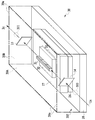
- FIG. 3 is a diagram showing the configuration of the wavelength converter 30 which is an embodiment of the present invention.
- the wavelength converter 30 When the fundamental wave having a wavelength of 1550 nm is input from the input port 300 as the signal light 1 a, the wavelength converter 30 outputs the wavelength-converted signal light 3 c having the wavelength (775 nm) that is the second harmonic of the fundamental wave from the output port 301. It is an output wavelength converter.
- the configuration of the wavelength conversion device 30 shown in FIG. 3 is the same as that of the wavelength conversion device 20 shown in FIG. The difference is that the substrate 32 of the wavelength conversion element 33 employs a ferroelectric crystal whose polarization direction is not a single polarization direction but a random polarization direction.
- the wavelength conversion device 30 includes a multiplexer 14 that combines the signal light 1a and control light (not shown), a wavelength conversion element 33 that includes an optical waveguide core 31 and a substrate 32, and a wavelength-converted signal light.
- a demultiplexer 15 for demultiplexing 3c and control light (not shown) is provided.
- a metal housing including a first portion 39A of the metal housing and a second portion 39B of the metal housing is provided so as to seal those elements, and the temperature control element 26 is further provided inside the metal housing.
- An upper member 27, and a metal casing bottom member 28 is provided inside the metal housing.
- the metal casing including the first portion 39A of the metal casing and the second portion 39B of the metal casing is an input port 300 for outputting and outputting an electric signal for inputting / outputting light and controlling temperature and an output.
- a port 301 is provided on the side surface.
- the multiplexer 14, the demultiplexer 15, and the signal light 1a are the same as those described with reference to FIG.
- the optical waveguide core 31 is an optical waveguide that selectively transmits the inside of the signal light 1a without losing its intensity.
- the structure of the optical waveguide core 31 is not particularly limited as long as it has a function of outputting the wavelength-converted signal light 3c having a wavelength different from that of the signal light 1a when the wavelength of the signal light 1a is input.
- the substrate 32 is a ferroelectric substance and is transparent to the signal light 1a, that is, a substrate that does not absorb light.
- the substrate 32 functions as an underclad with respect to the optical waveguide core 31 when forming a ridge type optical waveguide, and the signal light 1a, the control light (not shown), and the wavelength converted from the optical waveguide core 31 are converted. It is necessary that the refractive index of the signal light 3c is low.
- LiNbO 3 , KNbO 3 potassium niobate
- LiTaO 3 lithium tantalate
- LiNb (x) Ta (1-x) O 3 (0 ⁇ x ⁇ 1) Non-stoichiometric lithium tantalate
- KTiOPO 4 potassium titanate phosphate
- Mg magnesium
- Zn zinc
- Sc silver
- In indium
- the metal case is a metal case that joins the first part 39A of the metal case and the second part 39B of the metal case and seals the inside so as to keep the inside airtight.
- the upper member 27 is a metal member for uniformly controlling the temperature of the entire wavelength conversion element 33 including the optical waveguide core 31 and the substrate 32.
- the linear expansion coefficients of the upper member 27 and the metal casing bottom member 28 are controlled in order to suppress the deformation of the upper member 27 and the metal casing bottom member 28 due to the thermal stress generated by the temperature change of the temperature control element 26. It is preferable that the coefficient of linear expansion of the element 26 is substantially equal. Specifically, the linear expansion coefficient of the upper member 27 is preferably 10 ⁇ 10 ⁇ 6 / K or more and 20 ⁇ 10 ⁇ 6 / K or less.
- the material of the upper member preferably contains one or more metals selected from stainless steel, copper molybdenum steel, carbon steel, chrome molybdenum steel, copper, phosphorous deoxidized copper, oxygen-free copper, phosphor bronze, and brass. .. In this embodiment, oxygen-free copper is used as the upper member 27.
- the metal casing bottom surface member 28 is a member having high mechanical strength and high thermal conductivity for efficiently transmitting the heat generation and heat absorption effects of the temperature control element 26 to the wavelength conversion element 33.
- the linear expansion coefficient of the metal casing bottom member 28 is preferably 4 ⁇ 10 ⁇ 6 / K or more and 12 ⁇ 10 ⁇ 6 / K or less.
- the linear expansion coefficients of the upper member 27 and the metal casing bottom member 28 are both set to be substantially equal to the linear expansion coefficient of the temperature control element 26, so that the upper member 27 and the metal casing bottom member 28 are deformed by thermal stress. Can be further suppressed. That is, it is more preferable that the range of the value of the coefficient of linear expansion of the bottom member 28 of the metal housing is substantially equal to the range of the value of the coefficient of linear expansion of the upper member 27.
- the material of the bottom member of the metal casing preferably contains one or more metals selected from tungsten, molybdenum, kovar, copper tungsten steel, stainless steel, and copper molybdenum steel.
- stainless steel is used as the metal casing bottom member 28.
- the temperature control element 26 is inserted between the upper member 27 and the metal casing bottom member 28.
- the temperature control element 26 is a Peltier element. Further, in order to efficiently transmit the heat generation and heat absorption effects to the upper member 27 and the metal casing bottom surface member 28, a soldering method, a bonding method using a conductive adhesive, or another known bonding method is adopted as a method of bonding them. It is possible to
- the dry gas 302 is a gas that fills the inside of the metal housing and does not contain water. That is, as shown in FIG. 3, the dry gas 302 is an atmosphere around the wavelength conversion element 33, the temperature control element 26, the upper member 27, and the metal housing bottom surface member 28 which are sealed in the metal housing.
- the dry gas 302 preferably contains one or more selected from nitrogen, oxygen, argon, or helium.
- dry nitrogen gas is used as the dry gas 302.
- the substrate 32 is previously heated and cooled.
- a 0.5 mm-thick LiTaO 3 crystal as the substrate 32 was placed in an electric furnace and heated in a dry nitrogen gas atmosphere at 650 ° C. for 2 hours while maintaining the temperature. After the heating, the substrate 32 was cooled until its temperature dropped to room temperature.
- the direction of spontaneous polarization becomes random in the LiTaO 3 crystal that is the substrate 32.
- the electric fields due to random polarization cancel each other out inside the substrate 32, and the pyroelectric effect becomes smaller than in the case of unidirectional polarization, and the surface charge density of the substrate 32 can be made smaller.
- This ferroelectric substrate 32 was used as the lower part of the ridge type optical waveguide, and an optical waveguide core 31 of 5 ⁇ m square PPLN was formed on the substrate 32 by dry etching.
- the wavelength conversion element 33 manufactured as described above is fixed on the upper member 27, and the upper member 27, the metal housing bottom member 28, and the metal casing bottom member 28 inside the first portion 39A of the metal housing having an open top surface. And the temperature control element 26 was inserted between them, fixed and stored. After fixing, the metal casing was hermetically sealed by seam welding the first portion 39A of the metal casing and the first portion 39B of the metal casing in a dry nitrogen gas atmosphere. The joint portion by seam welding is 39e.
- FIG. 4 and 5 respectively show the phase matching of the wavelength conversion device 30 when the substrate 32 is not heated in advance in a dry nitrogen gas atmosphere at 650 ° C. for 2 hours (FIG. 4) and when it is heated (FIG. 5). It is a graph which shows a characteristic. 4 and 5, the horizontal axis represents the wavelength of the wavelength-converted signal light 3c output from the wavelength conversion device 30, and the vertical axis represents the output power thereof.
- the phase matching condition is not locally satisfied in the optical waveguide core 31 due to the change in the refractive index of the substrate 32 due to the pyroelectric property of the substrate 32, and is represented by a Sinc function which is a theoretical phase matching curve. It can be seen that the wavelength conversion efficiency is significantly deviated from the characteristics.
- the substrate 32 subjected to the heat treatment as shown in FIG. 5 is applied as the substrate of the wavelength conversion element, the phase matching characteristic when the substrate 32 shown in FIG.
- the shape of the phase matching curve approaches an ideal Sinc function, and high wavelength conversion efficiency can be obtained.
Landscapes
- Physics & Mathematics (AREA)
- Nonlinear Science (AREA)
- General Physics & Mathematics (AREA)
- Optics & Photonics (AREA)
- Chemical & Material Sciences (AREA)
- Crystallography & Structural Chemistry (AREA)
- Optical Modulation, Optical Deflection, Nonlinear Optics, Optical Demodulation, Optical Logic Elements (AREA)
Abstract
強誘電体基板を含む波長変換素子の温度を変化させたときに生じる焦電効果により招来される、波長変換された光の出力パワーの低下を抑制する。信号光が入力されたときに信号光の波長と異なる光を発生させる波長変換装置であって、信号光の波長を変換する波長変換素子と、波長変換素子の温度を制御するための温度制御素子と、を備え、波長変換素子および温度制御素子は、金属筐体の内部に密閉され、金属筐体の内部は窒素、酸素、アルゴン、またはヘリウムから選ばれる一種以上を含む乾燥ガスで充填されており、波長変換素子は、光導波路コアと光導波路コアよりも信号光に対して低い屈折率を有する基板とを含み、基板は、自発分極の方向がランダムな強誘電体である、波長変換装置を提供する。
Description
本発明は、波長変換装置に関する。
周期分極反転ニオブ酸リチウム(Periodically Poled Lithium Niobate、以下、PPLNという)を利用した光導波路は、導波路とすることによる光強度の増大化および疑似位相整合技術の利用による高い波長変換効率を実現可能な素子である。そのため、PPLNを利用した光導波路は、次世代光ファイバ通信分野や量子コンピューティングの分野で重要な役割を担うデバイスとして注目されている。このPPLNを利用した光導波路は、低雑音な光増幅が可能な位相感応増幅器(PSA)を構成するパラメトリック増幅素子および励起光発生素子として使用されており、高利得・低雑音な光増幅特性が実現されている。また量子コンピューティングの分野において、PPLNを利用した光導波路をファイバリング共振器内に挿入しパラメトリック発振素子として使用することで、従来の計算機に比べて極めて高速に大容量の計算を実証した報告がされている。これらの技術の更なる高性能化のためには、より高い波長変換効率を有する波長変換装置を実現することが重要となっている。
図1は、擬似位相整合(Quasi-Phase-Matched、以下、QPMという)技術により差周波を発生させる従来の波長変換装置10の基本構成を示す図である。図1の波長変換装置10の構成は、特許文献1に開示されている。図1に示すように、光強度が低い信号光1aおよび光強度の高い制御光1bは、合波器14に入射し合波される。制御光1bと合波した信号光1aは、基板12と基板12の上に配置される光導波路コア11を含む波長変換素子13に向かって進行する。周期分極反転構造を有して非線形光学効果を発現する光導波路コア11の一方の端に入射する。信号光1aは、光導波路コア11の中を通過する時に信号光1aと異なる波長を有する差周波光1cへと変換され、制御光1bと共に光導波路コア11の他方の端から出射される。光導波路コア11から出射した差周波光1cと制御光1bとは、分波器15に入射し互いに分離される。
また、擬似位相整合技術を利用して波長変換を行う光学素子(以下、波長変換素子という)を作製する方法もいくつか知られている。例えば、非線形光学効果を発現させる結晶(以下、非線形光学結晶という)基板を周期分極反転構造とした後に、その周期分極反転構造を用いてプロトン交換導波路を作製する方法である。また例えば、同様に、非線形光学結晶基板を周期分極反転構造とした後に、フォトリソグラフィプロセスおよびドライエッチングプロセスを利用してリッジ型光導波路を作製する方法である。
特許文献1には、これらのうちリッジ型光導波路を作製する例が開示されている。特許文献1には、リッジ型光導波路において、光の閉じ込め効果を向上させるため、周期分極反転構造を有する非線形光学結晶の第1の基板とその第1の基板の屈折率より小さい屈折率を有する第2の基板とを貼り合わせて波長変換素子を作製することが記載されている。また、特許文献1には、接着剤の劣化や温度変化によるクラックを回避するために、第1の基板と同種の非線形光学結晶を第2の基板として使用し、第1の基板と第2の基板とに熱を加えて拡散接合させることが記載されている。
波長変換素子を備える波長変換装置は、実用上、使用環境の変化により特性が劣化しない様に、光の入出力が可能な入出力ポートを備えた金属筐体内に合波器および分波器と共に波長変換素子を収納し使用することが知られている。さらに波長変換素子の波長変換効率は温度依存性を有しており、その波長変換効率を最大化するためは波長変換素子の温度を制御することが必要である。そのため波長変換装置は、さらに温度制御素子を金属筐体の内部に収納している。
図2は、図1の波長変換装置10の構成にさらに金属筐体29および温度制御素子26を備える波長変換装置20の構成例を示す図である。図2に示す波長変換装置の構成は図1に示す構成に加えて、金属筐体29、温度制御素子26、上部部材27、および金属筐体底面部材28を備えている。金属筐体29は、光の入出力および温度制御のための電気信号の入出力をするための入力ポート200および出力ポート201を側面に備えている。上部部材27は、光導波路コア11および基板12を含む波長変換素子13の全体の温度を均一に制御するための金属部材である。温度制御素子26は、上部部材27と金属筐体底面部材28との間に介挿されている。なお、光導波路コア11、基板12、波長変換素子13、合波器14、分波器15、信号光1a、差周波光1cは、図1の説明におけるものと同じであるため説明を省略する。
また、強誘電体結晶材料を用いた波長変換素子を波長変換装置に用いた場合、短い波長を有する光の照射により波長変換素子の屈折率が変化して特性が低下する光損傷と呼ばれる現象が生じる。この光損傷による影響を抑制する方法として波長変換素子を高温で使用することが提案されている。
波長変換素子を高温で動作させるためには、ヒーター等の熱源を用いて波長変換素子を加熱する方法が考えられる。例えば、図2に示す波長変換装置20では波長変換素子13の温度制御を高精度で高速に行うことが必要なため、温度制御素子26としてペルチェ素子を用いる。ペルチェ素子を用いて波長変換素子13の温度を高温に設定する場合、以下に説明する事象が問題となる。
ここで、ペルチェ素子は、ペルチェ素子に電流を流すと一方の面で吸熱が生じ同時に他方の面で発熱が生じる効果を利用する素子である。そのため、波長変換素子13の温度を波長変換素子13の周囲の温度よりも高温に設定する場合、大気環境下では吸熱側において結露が生じることが想定される。その結露により生じた水がペルチェ素子の内部やリード線電極付近に滞ると、ペルチェ素子とリード線電極とを接合する半田が水により腐食し、ペルチェ素子とリード線電極とが電気的に断線して破損する。または結露により生じた水が複数の電極と接触する場合、電極間の電位差により半田の成分が水を介してアノード溶出およびカソード析出を繰り返す結果、複数の電極がショートして波長変換素子13が故障する。そのため、信頼性の高い波長変換装置20を実現するためには、水を含まない乾燥ガス雰囲気で波長変換装置20を気密封止することが必要となる。
しかしながら、乾燥ガス雰囲気で波長変換装置20を気密封止すると、波長変換装置20の中に大気イオンが存在しないため、波長変換素子13の温度を変化させた際に強誘電体である基板12の焦電効果に起因して生じる基板12上の表面電荷を中和することができない。このとき、基板12の屈折率分布が発生する。さらに、基板12の表面における焦電効果による表面電荷の変化は、光導波路コア11の内部にも影響を与え光導波路コア11の内部の電荷密度に不均一な分布を生じさせる。そのため、光導波路コア11の内部にも不均一な屈折率分布が生じる。その結果、光導波路コア11において位相整合条件を満たす波長が変化し、波長変換された差周波光1cの出力パワーが低下するという課題があった。
本発明は、上記課題を解決するためになされたものである。本発明の一実施形態は、信号光が入力されたときに信号光の波長と異なる光を発生させる波長変換装置であって、信号光の波長を変換する波長変換素子と、波長変換素子の温度を制御するための温度制御素子と、を備える。ここで、波長変換素子および温度制御素子は、金属筐体の内部に密閉され、金属筐体の内部は窒素、酸素、アルゴン、またはヘリウムから選ばれる一種以上を含む乾燥ガスで充填されており、波長変換素子は、光導波路コアと光導波路コアよりも信号光に対して低い屈折率を有する基板とを含み、基板は、自発分極の方向がランダムな強誘電体である。
本発明により、強誘電体基板を含む波長変換素子の温度を変化させたときに生じる焦電効果により招来される、波長変換された光の出力パワーの低下を抑制可能な波長変換装置を提供することができる。
本発明の一実施形態の波長変換装置の動作原理について説明する。本発明の一実施形態の波長変換装置は、波長変換素子のリッジ型光導波路の下部である基板として強誘電体結晶を用いる。その基板を一度キュリー温度以上において加熱した後に冷却する。この加熱および冷却処理により、加熱前の分極方向と異なる方向の分極が誘電体結晶である基板中にランダムに生じるため、強誘電体の分極方向は単一ではなくなる。分極方向が単一でなくランダムな分極方向を有する強誘電体結晶は、それぞれ異なる方向の分極による電場が強誘電体結晶の内部で互いに打ち消しあうために、結果的として単一分極方向を有する強誘電体結晶よりも焦電効果が小さくなる。
すなわち、加熱前の基板は、巨視的かつ微視的に、自発分極の方向が一定の方向に揃っていて、加熱後の基板は、ドメイン内で自発分極の方向がランダムとなる部分が生じる。上記の、単一分極の強誘電体結晶よりも焦電効果が小さくなる効果は、基板の構造変化により実現されるものである。
この加熱および冷却処理の前後で、基板の特性である圧電性、電歪性、非線形光学特性は損なわれるものの、波長変換された光の出力パワーに影響を与える基板の屈折率、透過率、線膨張係数はほぼ変わらないという技術的特徴を有する。この技術的特徴を有することにより、本発明の一実施形態である波長変換装置は、乾燥ガス雰囲気中においても基板の焦電効果を抑制しながら使用することが可能である。
(実施例)
図3は、本発明の一実施形態である波長変換器30の構成を示す図である。波長変換器30は、信号光1aとして波長1550nmの基本波が入力ポート300から入力されると、その第二高調波である波長(775nm)を有する波長変換された信号光3cが出力ポート301から出力される波長変換装置である。図3に示す波長変換装置30の構成は、図2に示す波長変換装置20と同じである。異なるのは、波長変換素子33の基板32が、分極方向が単一でなくランダムな分極方向である強誘電体結晶を採用している点である。
図3は、本発明の一実施形態である波長変換器30の構成を示す図である。波長変換器30は、信号光1aとして波長1550nmの基本波が入力ポート300から入力されると、その第二高調波である波長(775nm)を有する波長変換された信号光3cが出力ポート301から出力される波長変換装置である。図3に示す波長変換装置30の構成は、図2に示す波長変換装置20と同じである。異なるのは、波長変換素子33の基板32が、分極方向が単一でなくランダムな分極方向である強誘電体結晶を採用している点である。
まず、波長変換装置30の構成について説明する。波長変換装置30は、信号光1aと制御光(図示せず)とを合波する合波器14と、光導波路コア31と基板32とを含む波長変換素子33と、波長変換された信号光3cと制御光(図示せず)とを分波する分波器15を備えている。それらの要素を密封するように、金属筐体の第1の部分39A,金属筐体の第2の部分39Bを含む金属筐体が備えられ、金属筐体の内部には、さらに温度制御素子26、上部部材27、および金属筐体底面部材28を備えている。
金属筐体の第1の部分39A,金属筐体の第2の部分39Bを含む金属筐体は、光の入出力および温度制御のための電気信号の入出力をするための入力ポート300および出力ポート301を側面に備えている。なお、合波器14、分波器15、信号光1aは、図1の説明におけるものと同じであるため説明を省略する。
光導波路コア31は、信号光1aの強度を損失させることなく、選択的にその内部を透過させる光導波路である。光導波路コア31の構造は、信号光1aの波長が入力された時に信号光1aと異なる波長を有する波長変換された信号光3cを出力する機能を有するものであれば特に限定はされない。二次の非線形定数が光の進行方向に沿って周期的にまたは所定の変調が付与された周期で変化し、単一の波長または複数の波長について疑似位相整合を実現する構造であって、例えば、マルチQPM素子を採用することも可能である。
基板32は、強誘電体であり信号光1aに対して透明、すなわち光吸収を生じない基板である。基板32は、リッジ型光導波路を構成する際に、光導波路コア31に対するアンダークラッドとして機能させるものであり、光導波路コア31よりも信号光1a、制御光(図示せず)、および波長変換された信号光3cに対して屈折率が低いことが必要である。
基板32に採用する強誘電体材料として、LiNbO3、KNbO3(ニオブ酸カリウム)、LiTaO3(タンタル酸リチウム)、LiNb(x)Ta(1-x)O3(0≦x≦1)(不定比組成のタンタル酸リチウム)、またはKTiOPO4(チタン酸リン酸カリウム)、さらに、それらにMg(マグネシウム)、Zn(亜鉛)、Sc(スカンジウム)、In(インジウム)から選ばれる少なくとも1つを添加物として含有しているものが好ましい。
金属筐体は、金属筐体の第1の部分39Aと金属筐体の第2の部分39Bとを接合して、内部の気密を保つように密閉する金属筐体である。
上部部材27は、光導波路コア31および基板32を含む波長変換素子33の全体の温度を均一に制御するための金属部材である。
ここで、上部部材27および金属筐体底面部材28の線膨張係数は、温度制御素子26の温度変化で生じる熱応力による上部部材27および金属筐体底面部材28の変形を抑制するために温度制御素子26の線膨張係数とほぼ等しいことが好ましい。具体的には上部部材27の線膨張係数は、10×10-6/K以上20×10-6/K以下であることが好ましい。
また、上部部材の材料は、ステンレス鋼、銅モリブデン鋼、炭素鋼、クロムモリブデン鋼、銅、リン脱酸銅、無酸素銅、リン青銅、または黄銅から選ばれる一種以上の金属を含むことが好ましい。本実施例では、上部部材27として無酸素銅を使用した。
金属筐体底面部材28は、機械的強度が高く、かつ温度制御素子26による発熱および吸熱効果を効率的に波長変換素子33に伝達するために高い熱伝導率を有する部材である。
金属筐体底面部材28の線膨張係数は、4×10⁻⁶/K以上12×10-6/K以下であることが好ましい。
さらに、上部部材27および金属筐体底面部材28の線膨張係数は、共に温度制御素子26の線膨張係数とほぼ等しく設定することにより、熱応力による上部部材27および金属筐体底面部材28の変形をさらに抑制することができる。すなわち、金属筐体底面部材28の線膨張係数の値の範囲は、上部部材27の線膨張係数の値の範囲と略等しいことがさらに好ましい。
また、金属筐体底面部材の材料は、タングステン、モリブデン、コバール、銅タングステン鋼、ステンレス鋼、または銅モリブデン鋼から選ばれる一種以上の金属を含むことが好ましい。本実施例では、金属筐体底面部材28としてステンレス鋼を使用した。
温度制御素子26は、上部部材27と金属筐体底面部材28との間に介挿されている。温度制御素子26は、ペルチェ素子である。さらに、上部部材27と金属筐体底面部材28とに発熱および吸熱効果を効率的に伝達するために、それらとの接合方法として半田接合、導電性接着剤による接合その他の公知の接合方法を採用することが可能である。
乾燥ガス302は、金属筐体の内部を充填し水を含まないガスである。すなわち、乾燥ガス302は、図3に示すように、金属筐体に密閉されている波長変換素子33、温度制御素子26、上部部材27、および金属筐体底面部材28の周囲の雰囲気である。
乾燥ガス302は、窒素、酸素、アルゴン、またはヘリウムから選ばれる一種以上を含むことが好ましい。本実施例では、乾燥ガス302として乾燥窒素ガスを使用した。
次に、波長変換装置30の作製方法について説明する。予め、基板32に対して加熱および冷却処理を行う。基板32として厚さ0.5mmのLiTaO3の結晶を電気炉に投入し、乾燥窒素ガス雰囲気において650℃で2時間、温度を維持しながら加熱した。その加熱後に、基板32の温度が室温に下がるまで冷却した。
この加熱および冷却処理を施すことにより、基板32であるLiTaO3の結晶中で自発分極の方向がランダムとなる。その結果、基板32の内部において、ランダムな分極による電場が互いに打ち消しあい、単一方向分極の場合と比較して焦電効果が小さくなり基板32の表面電荷密度を小さくすることが可能だった。
この強誘電体の基板32をリッジ型光導波路の下部として使用し、基板32の上に5μm角のPPLNによる光導波路コア31をドライエッチングにより形成した。
以上のように作製した波長変換素子33を上部部材27の上に固定し、上面が開口している金属筐体の第1の部分39Aの内側に、上部部材27、金属筐体底面部材28、およびそれらの間に温度制御素子26を介挿し、固定し収納した。固定後,乾燥窒素ガス雰囲気中で金属筐体の第1の部分39Aと金属筐体の第1の部分39Bとをシーム溶接することにより金属筐体の気密封止を行った。シーム溶接による接合箇所は、39eである。
図4および図5は、それぞれ、予め基板32を乾燥窒素ガス雰囲気中において650℃で2時間加熱をしていない場合(図4)と加熱した場合(図5)の波長変換装置30の位相整合特性を示すグラフである。図4および図5において、横軸は波長変換装置30から出力された波長変換された信号光3cの波長を、縦軸はそれらの出力パワーを示している。
図4において、基板32の焦電性に起因する基板32の屈折率変化により光導波路コア31において位相整合条件が局所的に満足されず、理論上の位相整合曲線であるSinc関数で表される特性から大幅にずれて波長変換効率が低下していることが分かる。これに対して、図5に示すように加熱処理を施した基板32を波長変換素子の基板として適用した場合は、図4に示す基板32に加熱および冷却処理を施さない場合の位相整合特性と比較して、焦電効果の影響をより良く抑制し、その位相整合曲線の形状は理想的なSinc関数に近づき高い波長変換効率を得ることが可能であることが分かる。
1a 信号光
1b 制御光
1c 差周波光
3c 波長変換された信号光
10、20、30 波長変換装置
11、31 光導波路コア
12、32 基板
13、33 波長変換素子
14 合波器
15 分波器
26 温度制御素子
27 上部部材
28 金属筐体底面部材
29 金属筐体
39A 金属筐体の第1の部分
39B 金属筐体の第2の部分
39e 金属筐体の第1の部分と金属筐体の第2の部分との接合部
200、300 入力ポート
201、301 出力ポート
302 乾燥ガス
1b 制御光
1c 差周波光
3c 波長変換された信号光
10、20、30 波長変換装置
11、31 光導波路コア
12、32 基板
13、33 波長変換素子
14 合波器
15 分波器
26 温度制御素子
27 上部部材
28 金属筐体底面部材
29 金属筐体
39A 金属筐体の第1の部分
39B 金属筐体の第2の部分
39e 金属筐体の第1の部分と金属筐体の第2の部分との接合部
200、300 入力ポート
201、301 出力ポート
302 乾燥ガス
Claims (9)
- 信号光が入力されたときに前記信号光の波長と異なる光を発生させる波長変換装置であって、
前記信号光の波長を変換する波長変換素子と、
前記波長変換素子の温度を制御するための温度制御素子と、を備え、
前記波長変換素子および前記温度制御素子は、金属筐体の内部に密閉され、前記金属筐体の内部は窒素、酸素、アルゴン、またはヘリウムから選ばれる1つ以上を含む乾燥ガスで充填されており、
前記波長変換素子は、光導波路コアと前記光導波路コアよりも前記信号光に対して低い屈折率を有する基板とを含み、
前記基板は、自発分極の方向がランダムな強誘電体である、
波長変換装置。 - 前記信号光と制御光とを合波する合波器と、
前記波長変換素子により、前記信号光の波長と異なる光と制御光とを分波する分波器と、
をさらに備える、請求項1に記載の波長変換装置。 - 前記温度制御素子は、ペルチェ素子であって、
前記ペルチェ素子は、上部部材の第1の面と前記金属筐体の底面に配置されている金属筐体底面部材との間に介挿されており、前記上部部材の前記第1の面に対向する前記上部部材の第2の面に前記波長変換素子が載置され、
前記上部部材は、金属部材であって、
前記上部部材および前記金属筐体底面部材の線膨張係数の値が、前記ペルチェ素子の線膨張係数と略等しい値である、
請求項1または2に記載の波長変換装置。 - 前記光導波路コアは、前記信号光の進行方向に沿って、前記光導波路コアの内部の二次の非線形定数が周期的にまたはランダムに変化する疑似位相整合構造を有している、
請求項1乃至3のいずれか一項に記載の波長変換装置。 - 前記基板は、LiNbO3(ニオブ酸リチウム)、KNbO3(ニオブ酸カリウム)、LiTaO3(タンタル酸リチウム)、LiNb(x)Ta(1-x)O3(0≦x≦1)(不定比組成のタンタル酸リチウム)、またはKTiOPO4(チタン酸リン酸カリウム)、さらに、それらにMg(マグネシウム)、Zn(亜鉛)、Sc(スカンジウム)、またはIn(インジウム)から選ばれる少なくとも1つを添加物として含有している、
請求項1乃至4のいずれか一項に記載の波長変換装置。 - 前記上部部材の線膨張係数は、10×10-6/K以上20×10-6/K以下である請求項3に記載の波長変換装置。
- 前記金属筐体底面部材の線膨張係数は、4×10⁻⁶/K以上12×10-6/K以下である請求項3に記載の波長変換装置。
- 前記上部部材の材料は、ステンレス鋼、銅モリブデン鋼、炭素鋼、クロムモリブデン鋼、銅、リン脱酸銅、無酸素銅、リン青銅、または黄銅から選ばれる1つ以上を含む請求項3または6に記載の波長変換装置。
- 前記金属筐体底面部材の材料は、タングステン、モリブデン、コバール、銅タングステン鋼、ステンレス鋼、または銅モリブデン鋼から選ばれる1つ以上を含む請求項3または7に記載の波長変換装置。
Priority Applications (2)
| Application Number | Priority Date | Filing Date | Title |
|---|---|---|---|
| CN201980075897.5A CN113168070B (zh) | 2018-11-20 | 2019-11-12 | 波长转换装置 |
| US17/294,209 US11971644B2 (en) | 2018-11-20 | 2019-11-12 | Wavelength conversion device |
Applications Claiming Priority (2)
| Application Number | Priority Date | Filing Date | Title |
|---|---|---|---|
| JP2018-217436 | 2018-11-20 | ||
| JP2018217436A JP7135771B2 (ja) | 2018-11-20 | 2018-11-20 | 波長変換装置 |
Publications (1)
| Publication Number | Publication Date |
|---|---|
| WO2020105509A1 true WO2020105509A1 (ja) | 2020-05-28 |
Family
ID=70773617
Family Applications (1)
| Application Number | Title | Priority Date | Filing Date |
|---|---|---|---|
| PCT/JP2019/044339 Ceased WO2020105509A1 (ja) | 2018-11-20 | 2019-11-12 | 波長変換装置 |
Country Status (4)
| Country | Link |
|---|---|
| US (1) | US11971644B2 (ja) |
| JP (1) | JP7135771B2 (ja) |
| CN (1) | CN113168070B (ja) |
| WO (1) | WO2020105509A1 (ja) |
Cited By (3)
| Publication number | Priority date | Publication date | Assignee | Title |
|---|---|---|---|---|
| US20220244616A1 (en) * | 2019-06-20 | 2022-08-04 | Nippon Telegraph And Telephone Corporation | Wavelength Conversion Apparatus |
| WO2023218667A1 (ja) * | 2022-05-13 | 2023-11-16 | 日本電信電話株式会社 | 波長変換装置 |
| WO2026009282A1 (ja) * | 2024-07-01 | 2026-01-08 | Ntt株式会社 | 波長変換装置 |
Families Citing this family (5)
| Publication number | Priority date | Publication date | Assignee | Title |
|---|---|---|---|---|
| JP7135771B2 (ja) * | 2018-11-20 | 2022-09-13 | 日本電信電話株式会社 | 波長変換装置 |
| US20240248369A1 (en) | 2021-05-20 | 2024-07-25 | Nippon Telegraph And Telephone Corporation | Optical amplification apparatus and optical amplification method |
| US12574136B2 (en) | 2021-05-21 | 2026-03-10 | Ntt, Inc. | Optical amplification system, optical amplification apparatus and optical amplification method |
| WO2023105722A1 (ja) * | 2021-12-09 | 2023-06-15 | 日本電信電話株式会社 | 波長変換装置 |
| US12386237B2 (en) * | 2022-05-13 | 2025-08-12 | Ntt Research, Inc. | Ultra-broadband mid-infrared generation in dispersion-engineered thin-film lithium niobate |
Citations (7)
| Publication number | Priority date | Publication date | Assignee | Title |
|---|---|---|---|---|
| JPH11103119A (ja) * | 1997-09-26 | 1999-04-13 | Fuji Photo Film Co Ltd | 固体レーザー |
| JP2001119090A (ja) * | 1999-10-21 | 2001-04-27 | Fuji Photo Film Co Ltd | 半導体発光装置の製造方法 |
| JP2002006353A (ja) * | 2000-06-20 | 2002-01-09 | Mitsubishi Cable Ind Ltd | 分極反転結晶 |
| US20030012480A1 (en) * | 2001-06-28 | 2003-01-16 | Valerio Pruneri | Integrated optical waveguide device |
| WO2006101034A1 (ja) * | 2005-03-18 | 2006-09-28 | Nippon Telegraph And Telephone Corporation | 周期分極反転構造の作製方法 |
| WO2012066596A1 (ja) * | 2010-11-17 | 2012-05-24 | パナソニック株式会社 | レーザ光源、レーザ加工装置、および半導体の加工方法 |
| JP2015225127A (ja) * | 2014-05-26 | 2015-12-14 | 日本電信電話株式会社 | 波長変換装置 |
Family Cites Families (16)
| Publication number | Priority date | Publication date | Assignee | Title |
|---|---|---|---|---|
| JPH1082921A (ja) * | 1996-09-06 | 1998-03-31 | Ngk Insulators Ltd | 光導波路基板、光導波路部品、第二高調波発生デバイスおよび光導波路基板の製造方法 |
| JP4199408B2 (ja) * | 2000-04-28 | 2008-12-17 | 富士フイルム株式会社 | 波長変換素子、波長変換素子の製造方法、及び波長変換モジュール |
| JP3753236B2 (ja) | 2001-11-02 | 2006-03-08 | 日本電信電話株式会社 | 波長変換素子用薄膜基板の製造方法及び波長変換素子の製造方法 |
| JP4517698B2 (ja) * | 2003-09-26 | 2010-08-04 | 三菱電機株式会社 | 波長変換レーザ装置 |
| JP2005202334A (ja) * | 2004-01-19 | 2005-07-28 | Nippon Telegr & Teleph Corp <Ntt> | 光波長変換モジュール |
| JP2005215060A (ja) * | 2004-01-27 | 2005-08-11 | Nippon Telegr & Teleph Corp <Ntt> | 波長変換素子およびその製造方法 |
| JP4548649B2 (ja) * | 2004-01-28 | 2010-09-22 | 株式会社日本製鋼所 | レーザ波長変換ユニット |
| JP2007316541A (ja) | 2006-05-29 | 2007-12-06 | Ntt Electornics Corp | 光学素子の製造方法及び光学素子 |
| JP2008117980A (ja) * | 2006-11-06 | 2008-05-22 | Sumitomo Osaka Cement Co Ltd | 光モジュール |
| JP2012078443A (ja) * | 2010-09-30 | 2012-04-19 | Dainippon Screen Mfg Co Ltd | 光学デバイス、光学デバイスの製造方法および露光装置 |
| TWI459110B (zh) * | 2011-03-02 | 2014-11-01 | Univ Nat Taiwan | 光學非線性晶體光波導及其製作方法 |
| JP2015215501A (ja) * | 2014-05-12 | 2015-12-03 | 日本電信電話株式会社 | 波長変換素子 |
| JP6348439B2 (ja) * | 2015-03-17 | 2018-06-27 | 日本電信電話株式会社 | 波長変換素子 |
| CN104880887A (zh) * | 2015-06-19 | 2015-09-02 | 天津大学 | 近化学计量比低掺杂Mg:PPLN全光波长转换器制作方法 |
| JP2018097159A (ja) * | 2016-12-14 | 2018-06-21 | 住友大阪セメント株式会社 | 薄板ln光制御デバイス |
| JP7135771B2 (ja) * | 2018-11-20 | 2022-09-13 | 日本電信電話株式会社 | 波長変換装置 |
-
2018
- 2018-11-20 JP JP2018217436A patent/JP7135771B2/ja active Active
-
2019
- 2019-11-12 CN CN201980075897.5A patent/CN113168070B/zh active Active
- 2019-11-12 US US17/294,209 patent/US11971644B2/en active Active
- 2019-11-12 WO PCT/JP2019/044339 patent/WO2020105509A1/ja not_active Ceased
Patent Citations (7)
| Publication number | Priority date | Publication date | Assignee | Title |
|---|---|---|---|---|
| JPH11103119A (ja) * | 1997-09-26 | 1999-04-13 | Fuji Photo Film Co Ltd | 固体レーザー |
| JP2001119090A (ja) * | 1999-10-21 | 2001-04-27 | Fuji Photo Film Co Ltd | 半導体発光装置の製造方法 |
| JP2002006353A (ja) * | 2000-06-20 | 2002-01-09 | Mitsubishi Cable Ind Ltd | 分極反転結晶 |
| US20030012480A1 (en) * | 2001-06-28 | 2003-01-16 | Valerio Pruneri | Integrated optical waveguide device |
| WO2006101034A1 (ja) * | 2005-03-18 | 2006-09-28 | Nippon Telegraph And Telephone Corporation | 周期分極反転構造の作製方法 |
| WO2012066596A1 (ja) * | 2010-11-17 | 2012-05-24 | パナソニック株式会社 | レーザ光源、レーザ加工装置、および半導体の加工方法 |
| JP2015225127A (ja) * | 2014-05-26 | 2015-12-14 | 日本電信電話株式会社 | 波長変換装置 |
Cited By (5)
| Publication number | Priority date | Publication date | Assignee | Title |
|---|---|---|---|---|
| US20220244616A1 (en) * | 2019-06-20 | 2022-08-04 | Nippon Telegraph And Telephone Corporation | Wavelength Conversion Apparatus |
| US11733584B2 (en) * | 2019-06-20 | 2023-08-22 | Nippon Telegraph And Telephone Corporation | Wavelength conversion apparatus |
| WO2023218667A1 (ja) * | 2022-05-13 | 2023-11-16 | 日本電信電話株式会社 | 波長変換装置 |
| JPWO2023218667A1 (ja) * | 2022-05-13 | 2023-11-16 | ||
| WO2026009282A1 (ja) * | 2024-07-01 | 2026-01-08 | Ntt株式会社 | 波長変換装置 |
Also Published As
| Publication number | Publication date |
|---|---|
| US20220004081A1 (en) | 2022-01-06 |
| JP2020086031A (ja) | 2020-06-04 |
| CN113168070B (zh) | 2025-01-10 |
| CN113168070A (zh) | 2021-07-23 |
| JP7135771B2 (ja) | 2022-09-13 |
| US11971644B2 (en) | 2024-04-30 |
Similar Documents
| Publication | Publication Date | Title |
|---|---|---|
| JP7135771B2 (ja) | 波長変換装置 | |
| Umeki et al. | Highly efficient wavelength converter using direct-bonded PPZnLN ridge waveguide | |
| US10274809B1 (en) | Multiwavelength laser source | |
| JP2693582B2 (ja) | 波長変換素子 | |
| US11815785B2 (en) | Wavelength conversion optical element | |
| WO2011045893A1 (ja) | 光学素子の製造方法 | |
| JP5074436B2 (ja) | 高調波発生素子 | |
| CN113540933A (zh) | 一种基于同步双光参量过程的中红外参量激光器 | |
| Gu et al. | Difference‐Frequency Generation of 0.2‐mJ 3‐Cycle 9‐µm Pulses from Two 1‐kHz Multicycle OPCPAs | |
| JP7319582B2 (ja) | 波長変換装置 | |
| CN102165366B (zh) | 光波长变换元件、波长变换激光装置以及图像显示装置 | |
| JP7273338B2 (ja) | 波長変換装置 | |
| Kundys et al. | Numerical Study of Reconfigurable Mid‐IR Single Photon Sources Based on Functional Ferroelectrics | |
| JP4912387B2 (ja) | 非線形光素子 | |
| CN105449494A (zh) | 基于波导结构的内调制太赫兹源及其内调制方法 | |
| JP7553868B2 (ja) | 波長変換装置及び波長変換装置の製造方法 | |
| JP2016173429A (ja) | 波長変換素子 | |
| Lu et al. | Broadcast wavelength conversion based on cascaded χ (2) nonlinearity in MgO-doped periodically poled LiNbO3 | |
| Tadanaga et al. | Efficient 1.55 µm-band quasi-phase-matched ZnO-doped LiNbO3 wavelength converter with high damage resistance | |
| WO2022219687A1 (ja) | 波長変換光学素子 | |
| JP2899345B2 (ja) | 光学装置 | |
| JP4977119B2 (ja) | 波長変換素子及びその製造方法 | |
| Mondal et al. | Design of an optical amplifier for amplified OSC in IOTA facility at Fermilab | |
| Liu et al. | An optical metamixer | |
| Ababaike et al. | Mid-infrared 3.468 μm optical vortex parametric oscillator based on KTA |
Legal Events
| Date | Code | Title | Description |
|---|---|---|---|
| 121 | Ep: the epo has been informed by wipo that ep was designated in this application |
Ref document number: 19887562 Country of ref document: EP Kind code of ref document: A1 |
|
| NENP | Non-entry into the national phase |
Ref country code: DE |
|
| 122 | Ep: pct application non-entry in european phase |
Ref document number: 19887562 Country of ref document: EP Kind code of ref document: A1 |
|
| WWG | Wipo information: grant in national office |
Ref document number: 201980075897.5 Country of ref document: CN |