WO2020105456A1 - β型サイアロン蛍光体および発光装置 - Google Patents
β型サイアロン蛍光体および発光装置Info
- Publication number
- WO2020105456A1 WO2020105456A1 PCT/JP2019/043689 JP2019043689W WO2020105456A1 WO 2020105456 A1 WO2020105456 A1 WO 2020105456A1 JP 2019043689 W JP2019043689 W JP 2019043689W WO 2020105456 A1 WO2020105456 A1 WO 2020105456A1
- Authority
- WO
- WIPO (PCT)
- Prior art keywords
- sialon phosphor
- phosphor
- sialon
- light emitting
- primary particles
- Prior art date
- Legal status (The legal status is an assumption and is not a legal conclusion. Google has not performed a legal analysis and makes no representation as to the accuracy of the status listed.)
- Ceased
Links
Images


Classifications
-
- C—CHEMISTRY; METALLURGY
- C09—DYES; PAINTS; POLISHES; NATURAL RESINS; ADHESIVES; COMPOSITIONS NOT OTHERWISE PROVIDED FOR; APPLICATIONS OF MATERIALS NOT OTHERWISE PROVIDED FOR
- C09K—MATERIALS FOR MISCELLANEOUS APPLICATIONS, NOT PROVIDED FOR ELSEWHERE
- C09K11/00—Luminescent materials, e.g. electroluminescent or chemiluminescent
- C09K11/08—Luminescent materials, e.g. electroluminescent or chemiluminescent containing inorganic luminescent materials
-
- C—CHEMISTRY; METALLURGY
- C09—DYES; PAINTS; POLISHES; NATURAL RESINS; ADHESIVES; COMPOSITIONS NOT OTHERWISE PROVIDED FOR; APPLICATIONS OF MATERIALS NOT OTHERWISE PROVIDED FOR
- C09K—MATERIALS FOR MISCELLANEOUS APPLICATIONS, NOT PROVIDED FOR ELSEWHERE
- C09K11/00—Luminescent materials, e.g. electroluminescent or chemiluminescent
- C09K11/08—Luminescent materials, e.g. electroluminescent or chemiluminescent containing inorganic luminescent materials
- C09K11/77—Luminescent materials, e.g. electroluminescent or chemiluminescent containing inorganic luminescent materials containing rare earth metals
- C09K11/7728—Luminescent materials, e.g. electroluminescent or chemiluminescent containing inorganic luminescent materials containing rare earth metals containing europium
- C09K11/77348—Silicon Aluminium Nitrides or Silicon Aluminium Oxynitrides
-
- C—CHEMISTRY; METALLURGY
- C09—DYES; PAINTS; POLISHES; NATURAL RESINS; ADHESIVES; COMPOSITIONS NOT OTHERWISE PROVIDED FOR; APPLICATIONS OF MATERIALS NOT OTHERWISE PROVIDED FOR
- C09K—MATERIALS FOR MISCELLANEOUS APPLICATIONS, NOT PROVIDED FOR ELSEWHERE
- C09K11/00—Luminescent materials, e.g. electroluminescent or chemiluminescent
- C09K11/08—Luminescent materials, e.g. electroluminescent or chemiluminescent containing inorganic luminescent materials
- C09K11/61—Luminescent materials, e.g. electroluminescent or chemiluminescent containing inorganic luminescent materials containing fluorine, chlorine, bromine, iodine or unspecified halogen elements
-
- C—CHEMISTRY; METALLURGY
- C09—DYES; PAINTS; POLISHES; NATURAL RESINS; ADHESIVES; COMPOSITIONS NOT OTHERWISE PROVIDED FOR; APPLICATIONS OF MATERIALS NOT OTHERWISE PROVIDED FOR
- C09K—MATERIALS FOR MISCELLANEOUS APPLICATIONS, NOT PROVIDED FOR ELSEWHERE
- C09K11/00—Luminescent materials, e.g. electroluminescent or chemiluminescent
- C09K11/08—Luminescent materials, e.g. electroluminescent or chemiluminescent containing inorganic luminescent materials
- C09K11/64—Luminescent materials, e.g. electroluminescent or chemiluminescent containing inorganic luminescent materials containing aluminium
-
- C—CHEMISTRY; METALLURGY
- C09—DYES; PAINTS; POLISHES; NATURAL RESINS; ADHESIVES; COMPOSITIONS NOT OTHERWISE PROVIDED FOR; APPLICATIONS OF MATERIALS NOT OTHERWISE PROVIDED FOR
- C09K—MATERIALS FOR MISCELLANEOUS APPLICATIONS, NOT PROVIDED FOR ELSEWHERE
- C09K11/00—Luminescent materials, e.g. electroluminescent or chemiluminescent
- C09K11/08—Luminescent materials, e.g. electroluminescent or chemiluminescent containing inorganic luminescent materials
- C09K11/77—Luminescent materials, e.g. electroluminescent or chemiluminescent containing inorganic luminescent materials containing rare earth metals
- C09K11/7728—Luminescent materials, e.g. electroluminescent or chemiluminescent containing inorganic luminescent materials containing rare earth metals containing europium
- C09K11/7734—Aluminates
-
- H—ELECTRICITY
- H10—SEMICONDUCTOR DEVICES; ELECTRIC SOLID-STATE DEVICES NOT OTHERWISE PROVIDED FOR
- H10H—INORGANIC LIGHT-EMITTING SEMICONDUCTOR DEVICES HAVING POTENTIAL BARRIERS
- H10H20/00—Individual inorganic light-emitting semiconductor devices having potential barriers, e.g. light-emitting diodes [LED]
- H10H20/80—Constructional details
- H10H20/85—Packages
- H10H20/851—Wavelength conversion means
-
- H—ELECTRICITY
- H10—SEMICONDUCTOR DEVICES; ELECTRIC SOLID-STATE DEVICES NOT OTHERWISE PROVIDED FOR
- H10H—INORGANIC LIGHT-EMITTING SEMICONDUCTOR DEVICES HAVING POTENTIAL BARRIERS
- H10H20/00—Individual inorganic light-emitting semiconductor devices having potential barriers, e.g. light-emitting diodes [LED]
- H10H20/80—Constructional details
- H10H20/85—Packages
- H10H20/851—Wavelength conversion means
- H10H20/8511—Wavelength conversion means characterised by their material, e.g. binder
- H10H20/8512—Wavelength conversion materials
-
- H—ELECTRICITY
- H10—SEMICONDUCTOR DEVICES; ELECTRIC SOLID-STATE DEVICES NOT OTHERWISE PROVIDED FOR
- H10H—INORGANIC LIGHT-EMITTING SEMICONDUCTOR DEVICES HAVING POTENTIAL BARRIERS
- H10H20/00—Individual inorganic light-emitting semiconductor devices having potential barriers, e.g. light-emitting diodes [LED]
- H10H20/80—Constructional details
- H10H20/85—Packages
- H10H20/851—Wavelength conversion means
- H10H20/8511—Wavelength conversion means characterised by their material, e.g. binder
- H10H20/8512—Wavelength conversion materials
- H10H20/8513—Wavelength conversion materials having two or more wavelength conversion materials
-
- Y—GENERAL TAGGING OF NEW TECHNOLOGICAL DEVELOPMENTS; GENERAL TAGGING OF CROSS-SECTIONAL TECHNOLOGIES SPANNING OVER SEVERAL SECTIONS OF THE IPC; TECHNICAL SUBJECTS COVERED BY FORMER USPC CROSS-REFERENCE ART COLLECTIONS [XRACs] AND DIGESTS
- Y02—TECHNOLOGIES OR APPLICATIONS FOR MITIGATION OR ADAPTATION AGAINST CLIMATE CHANGE
- Y02B—CLIMATE CHANGE MITIGATION TECHNOLOGIES RELATED TO BUILDINGS, e.g. HOUSING, HOUSE APPLIANCES OR RELATED END-USER APPLICATIONS
- Y02B20/00—Energy efficient lighting technologies, e.g. halogen lamps or gas discharge lamps
Definitions
- the present invention relates to a ⁇ -sialon phosphor and a light emitting device.
- a light emitting device in which a light emitting element that emits primary light and a phosphor that absorbs primary light and emits secondary light are combined.
- the demand for heat resistance and durability of phosphors has increased with the increase in the output of light emitting devices, and ⁇ -sialon phosphors having a stable crystal structure have attracted attention.
- the phosphor having Eu 2+ as a solid solution in the crystal structure of ⁇ -sialon is a phosphor that emits green light of 520 to 550 nm when excited by ultraviolet to blue light.
- the ⁇ -sialon in which Eu 2+ is solid-dissolved is also called Eu solid-solution ⁇ -sialon.
- This phosphor is used as a green light emitting component of a light emitting device such as a white light emitting diode (referred to as a white LED (Light Emitting Diode)).
- the Eu solid solution ⁇ -sialon has a very sharp emission spectrum among the phosphors in which Eu 2+ is solid-solved, and is particularly a liquid crystal that requires narrow band emission consisting of the three primary colors of blue, green, and red light. It is a phosphor suitable for a green light emitting component of a backlight light source of a display panel.
- Patent Document 1 As a technique related to such ⁇ -sialon phosphor, for example, the technique described in Patent Document 1 below can be cited.
- Patent Document 1 International Publication No. 2012/011444 discloses a compound represented by the general formula: Si 6-Z Al Z O Z N 8-Z (0 ⁇ Z ⁇ 0.42), and ⁇ is a solid solution of Eu.
- Type sialon in which the 50% area average diameter of the primary particles of the ⁇ type sialon is 5 ⁇ m or more is described.
- the present invention has been made in view of the above circumstances.
- the present invention provides a ⁇ -sialon phosphor having improved brightness and a light emitting device.
- the present inventors have earnestly studied to provide a ⁇ -sialon phosphor and a light emitting device with improved brightness. As a result, it has been found that the brightness of the ⁇ -sialon phosphor and the light emitting device using the same can be improved by setting the respective D 50 and (D 50 ⁇ D 10 ) / D 50 described below in specific ranges. Invented.
- the following ⁇ -sialon phosphor and light emitting device are provided.
- a ⁇ -sialon phosphor in which europium is dissolved When the crystal orientation in each particle of the ⁇ -sialon phosphor is identified by the electron backscattering diffraction image method and the single crystal particles distinguished for each crystal orientation are defined as primary particles, When the cross-sectional area of the primary particles is obtained by image analysis, The 50% area average diameter of the primary particles of the ⁇ -sialon phosphor is D 50 , When the 10% area average diameter of the primary particles of the ⁇ -sialon phosphor is defined as D 10 , D 50 is 7.0 ⁇ m or more and 20.0 ⁇ m or less, A ⁇ -sialon phosphor having (D 50 ⁇ D 10 ) / D 50 of 0.60 or less.
- the D V50 particle size of the ⁇ -sialon phosphor is 50 ⁇ m or more and 50 ⁇ m or less (50% diameter in volume-based cumulative fraction by laser diffraction scattering method according to JIS R1629: 1997). 5. 1. Through 4. In the ⁇ -sialon phosphor according to any one of When a plurality of the primary particles are defined as secondary particles by sintering particles through grain boundaries, A ⁇ -sialon phosphor having a ratio of the number of primary particles to the number of secondary particles of the ⁇ -sialon phosphor of 1.90 or less. 6.
- the wavelength conversion member includes a phosphor,
- the phosphor is 1. Through 5.
- the light emitting source includes an LED chip that emits light having a wavelength of 300 nm to 500 nm. 8. 6. Or 7.
- the phosphor further includes a KSF-based phosphor in which manganese is solid-dissolved.
- FIG. 3 is a diagram showing a scanning electron microscope image (SEM image; Scanning Electron Microscope image) of the ⁇ -sialon phosphor of Example 1. It is a figure which shows the EBSD image by the EBSD method of the (beta) -sialon fluorescent substance shown in FIG.
- the ⁇ -sialon phosphor according to the present embodiment is a ⁇ -sialon phosphor in which europium is solid-soluted, and the 50% area average diameter of primary particles of the ⁇ -sialon phosphor is 50 , and the ⁇ -sialon is When the 10% area average diameter of primary particles of the phosphor is D 10 , the above D 50 is 7.0 ⁇ m or more and 20.0 ⁇ m or less, and (D 50 ⁇ D 10 ) / D 50 is 0.60 or less. ..
- the “primary particle” is defined as a single crystal particle in which the crystal orientation of each particle of the ⁇ -sialon phosphor is identified by the electron backscattering diffraction image method and distinguished for each crystal orientation. Further, D 50 and D 10 are obtained by image analysis of the cross-sectional area of the primary particles. A specific measuring method will be described later.
- the ⁇ -sialon phosphor according to the present embodiment is represented by, for example, the general formula Si 6-z Al z O z N 8-z : Eu 2+ (0 ⁇ Z ⁇ 4.2), and solid-dissolves Eu 2+. It is a phosphor made of ⁇ -sialon.
- the ⁇ -sialon in which europium is solid-dissolved is also simply referred to as ⁇ -sialon.
- the Z value and the content of europium are not particularly limited, but the Z value is, for example, more than 0 and 4.2 or less, and ⁇ -type. From the viewpoint of further improving the emission intensity of the sialon phosphor, it is preferably 0.005 or more and 1.0 or less. Further, the content of europium is preferably 0.1% by mass or more and 2.0% by mass or less.
- the ⁇ -sialon phosphor is one in which a plurality of particles are firmly integrated during the heat treatment in the firing process, and each one of the plurality of particles is a primary particle and a plurality of particles are firmly integrated.
- secondary particles More specifically, as described above, the primary particle is defined as a single crystal particle in which the crystal orientation in each particle of the ⁇ -sialon phosphor is identified by the electron backscattering diffraction image method and distinguished for each crystal orientation. can do. Further, the secondary particles can be defined as particles obtained by sintering a plurality of primary particles via grain boundaries.
- the emission intensity that is, the brightness is improved.
- the emission intensity that is, the brightness is improved.
- the particle size of the primary particles of the ⁇ -sialon phosphor is large, the proportion of impurities existing in the crystal grain boundaries is reduced and the crystallinity is improved, so that the luminous efficiency can be improved.
- the D 50 and (D 50 ⁇ D 10 ) / D 50 of the primary particles of the ⁇ -sialon phosphor are within the above range, the proportion of ⁇ -sialon particles having a small primary particle diameter and a low luminous efficiency is obtained.
- the ratio becomes relatively small, and the proportion of ⁇ -sialon particles having a large primary particle size and high emission efficiency becomes relatively large.
- the emission intensity of the ⁇ -sialon phosphor can be improved.
- the D 50 and (D 50 ⁇ D 10 ) / D 50 of the primary particles of the ⁇ -sialon phosphor are, as will be described later, two europium compounds that are one of the raw materials of the ⁇ -sialon phosphor. This can be realized by adding the compound in multiple times and performing the firing step, and by adding a larger amount of the europium compound than in the conventional case in the second firing step.
- the 50% area average diameter of the primary particles of the ⁇ -sialon phosphor according to the present embodiment has a D 50 of 7.0 ⁇ m or more and 20.0 ⁇ m or less, preferably 9.0 ⁇ m or more, and preferably 18.0 ⁇ m. Or less, more preferably 15.0 ⁇ m or less. Further, (D 50 ⁇ D 10 ) / D 50 is 0.60 or less, preferably 0.55 or less, more preferably 0.53 or less, and further preferably 0.51 or less. This can reduce the difference in characteristics between the ⁇ -sialon particles. As a result, it is possible to reduce variations in light emission characteristics and colors of the obtained light emitting device.
- (D 90 ⁇ D 10 ) / D 50 is preferably 1.45 or less, and more preferably 1.35 or less. Further, when (D 90 ⁇ D 10 ) / D 50 is not more than the above upper limit value, the difference in characteristics between ⁇ -sialon particles can be reduced. As a result, it is possible to reduce variations in light emission characteristics and colors of the obtained light emitting device.
- the 50% area average diameter D 50 , 10% area average diameter D 10 and 90% area average diameter D 90 of the primary particles will be described more specifically.
- Individual primary particles of the ⁇ -sialon phosphor that is, single crystal particles are arranged in order from the smallest cross-sectional area as C A1 , C A2 , C A3 , ..., C Ai , ..., C Ak.
- the term "primary particles” as used herein means all single-crystal particles, and a plurality of primary particles are sintered through grain boundaries to form secondary particles, and secondary particles are formed. Including without distinction.
- the cumulative curve is calculated with the total cross-sectional area (C A1 + C A2 + C A3 + ...
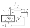
- FIG. 1 is a schematic diagram showing the configuration of an apparatus used for the measurement of the EBSD method. As shown in FIG. 1, the apparatus 1 used for the EBSD method is composed of a scanning electron microscope 2 and an electron backscattering diffraction image measuring apparatus 3 added thereto.
- the scanning electron microscope 2 includes a lens barrel section 2A, a stage section 2B on which a sample 4 is mounted, a stage control section 2C, an electron beam scanning section 2D, a control computer 2E, and the like.
- the electron backscattering diffractometry apparatus 3 includes a fluorescent screen 7 for detecting electrons 6 generated by irradiating a sample 4 with an electron beam 5 and scattered backward, and a camera 8 for capturing a fluorescent image of the fluorescent screen 7. And software and the like for obtaining and analyzing data of electron backscattering diffraction images (not shown).
- the ⁇ -sialon phosphor that is the sample 4 is irradiated with an electron beam to cause electron scattering corresponding to the crystal structure and the crystal plane, and the shape of the electron scattering pattern is analyzed by software. .. More specifically, the crystal orientation of each phosphor particle is identified, and the cross-sectional area of the primary particles that can be distinguished for each crystal orientation is determined by image analysis. Then, a cumulative curve is created from the obtained cross-sectional area as described above, and the cross-sectional areas (S 50 , S 10 , S 90 ) of the primary particles at points corresponding to 50%, 10% and 90% are obtained, and these are calculated.
- the 50% area average diameter D 50 , 10% area average diameter D 10 and 90% area average diameter of the primary particles corresponding to the diameter when converted to a circle are used.
- S 50 is the area of the primary particles at which the cumulative curve of the areas of the individual primary particles becomes 50%.
- 10% area average diameter of primary particles 2 ⁇ (S 10 / ⁇ ) 1/2
- S 10 is the area of the primary particles at which the cumulative curve of the areas of the individual primary particles becomes 10%.
- 90% area average diameter of primary particles 2 ⁇ (S 90 / ⁇ ) 1/2
- S 90 is the area of the primary particles at which the cumulative curve of the areas of the individual primary particles becomes 90%.
- the V50 particle diameter (50% volume average diameter) is preferably 50 ⁇ m or less, more preferably 40 ⁇ m or less, and further preferably 30 ⁇ m or less. Further, the DV50 particle size (50% volume average diameter) of the ⁇ -sialon phosphor according to the present embodiment is preferably 5 ⁇ m or more, and more preferably 10 ⁇ m or more.
- the “D V50 particle diameter (50% volume average diameter)” means a 50% diameter in a volume-based cumulative fraction by a laser diffraction scattering method according to JIS R1629: 1997. Note that the definition and measurement of D V50 particle size (50% volume average diameter) is different from the definition and measurement of D 50 , D 10 and D 90 .
- the ratio of the number of primary particles to the number of secondary particles of the ratio of the number of primary particles to the number of secondary particles of this ⁇ -sialon phosphor is the number of secondary particles in the image of ⁇ -sialon obtained by the EBSD method, It is calculated by counting the number of primary particles constituting secondary particles and taking the ratio of the number of primary particles to the number of secondary particles.
- the ratio of the number of primary particles to the number of secondary particles of the ⁇ -sialon phosphor is preferably 1.90 or less, more preferably 1.80 or less, It is more preferably 1.70 or less and even more preferably 1.60 or less. Further, when the ratio of the number of primary particles to the number of secondary particles of the ⁇ -sialon phosphor is not more than the above upper limit value, the difference in characteristics between the ⁇ -sialon particles can be reduced, and as a result, the resulting light emitting device can be obtained. It is possible to reduce variations in the light emission characteristics and colors.
- the ⁇ -sialon according to this embodiment is excited in a wide wavelength range from ultraviolet rays to visible light, and highly efficiently emits green light having a main wavelength in the range of 520 nm to 550 nm. Therefore, it is excellent as a green light emitting phosphor.
- the ⁇ -sialon phosphor according to the present embodiment can be preferably used as a material for a phosphor layer in a light emitting element.
- the light emitting element can be applied to a light source such as a backlight source of a display and a lighting device.
- the light emitting element is not particularly limited, but includes, for example, an LED and a phosphor layer laminated on the light emitting surface side of the LED.
- an ultraviolet LED or a blue LED which emits light having a wavelength of 300 to 500 nm, and particularly a blue LED which emits light having a wavelength of 440 to 480 nm can be used.
- the ⁇ -sialon phosphor obtained by the manufacturing method according to the present embodiment is excited by a wide range of wavelengths from ultraviolet to blue light, and exhibits high-intensity green light emission. Therefore, white light having blue or ultraviolet light as a light source is excited. It can be suitably used as a phosphor for an LED.
- the method for producing the ⁇ -sialon phosphor according to the present embodiment is different from the conventional method for producing the ⁇ -sialon phosphor. That is, the ⁇ -sialon phosphor in which the 50% area average diameter D 50 and (D 50 ⁇ D 10 ) / D 50 of the primary particles are within the above range is a europium compound which is one of the raw materials of the ⁇ -sialon phosphor.
- the ⁇ -sialon phosphor according to the present embodiment can adopt various other specific manufacturing conditions, for example, on the assumption that the above-mentioned manufacturing method is adopted.
- the method for producing a ⁇ -sialon phosphor according to this embodiment includes at least the following two firing steps. That is, the manufacturing method of the ⁇ -sialon phosphor according to the present embodiment, the first raw material powder containing the first europium compound is fired, the first firing step to obtain a first fired powder containing ⁇ -sialon particles, A second firing step of firing the obtained first fired powder and the second raw material powder containing the second europium compound to obtain the ⁇ -sialon phosphor according to the present embodiment.
- the second europium compound is added more than the conventional standard.
- the second europium compound is added so that the amount of Eu is more than the amount of Eu that can be solid-dissolved in ⁇ -sialon.
- the second firing step by adding the second europium compound so that the Eu amount becomes larger than the Eu amount that can be solid-dissolved in the ⁇ -sialon, the liquid phase during the firing of the ⁇ -sialon particles in the second firing step is performed.
- the primary particles of ⁇ -sialon particles having a small particle size can be made coarser. This makes it possible to adjust the 50% area average diameter D 50 and (D 50 ⁇ D 10 ) / D 50 of the primary particles of the ⁇ -sialon phosphor within the above range.
- the method for producing the ⁇ -sialon phosphor may further include one or more third firing steps for further firing the second fired powder to obtain the third fired powder. At that time, a europium compound may be further added.
- the “first firing step” means the first firing step of heat-treating the raw material powder containing the first europium compound
- the “second firing step” means the second europium. It means a second firing step of adding a compound and heat treatment
- the “third firing step” means a firing step performed after the second firing step.
- the "first europium compound” means a europium compound added in the first firing step
- the “second europium compound” means a europium compound added in the second firing step.
- the “first raw material powder” means the raw material powder used in the first firing step
- the “second raw material powder” is the raw material powder used in the second firing step.
- the respective raw material powders are mixed.
- the "first baked powder” means a product obtained in the first baking step
- the "second baked powder” means a product obtained in the second baking step.
- the "third baked powder” means the product obtained in the third baking step.
- the term “process” includes not only an independent process but also a term that is included in this term if the intended purpose of the process is achieved even when it cannot be clearly distinguished from other processes. Be done.
- the content of europium in the composition means the total amount of the plurality of materials present in the composition, unless otherwise specified, when there are a plurality of materials corresponding to europium in the composition.
- the first raw material powder preferably contains silicon nitride and aluminum nitride in addition to the first europium compound.
- Silicon nitride and an aluminum compound are materials for forming a skeleton of ⁇ -sialon, and a europium compound is a material for forming an emission center.
- the first raw material powder may further contain ⁇ -sialon.
- ⁇ -sialon is an aggregate or core material.
- the form of each of the above-mentioned components contained in the first raw material powder is not particularly limited, but it is preferable that all are in powder form.
- the europium compound is not particularly limited, and examples thereof include oxides containing europium, hydroxides containing europium, nitrides containing europium, oxynitrides containing europium, and halides containing europium. These may be used alone or in combination of two or more. Among these, europium oxide, europium nitride and europium fluoride are preferably used alone, and more preferably europium oxide is used alone.
- the europium compound is added separately before firing in multiple firing steps. Specifically, the europium compound is added before the firing in the first firing step and the second firing step, respectively.
- europium is divided into those that form a solid solution in ⁇ -sialon, those that volatilize, and those that remain as a heterophasic component.
- the heterophasic component containing europium can be removed by acid treatment or the like, but if it is produced in a too large amount, an insoluble component is produced by the acid treatment and the brightness is reduced. Further, as long as it is a different phase that does not absorb extra light, it may remain, or europium may be contained in this different phase.
- a ⁇ -sialon phosphor raw material other than the europium compound may be added together with the europium compound.
- the proportion of the second europium compound is preferably 1.0% by mass or more, more preferably 2.0% by mass or more, and further preferably Is 3.0% by mass or more, and the proportion of the second europium compound is preferably from the viewpoint of reducing the amount of insoluble heterophase components generated by acid treatment and further improving the brightness of the obtained ⁇ -sialon phosphor.
- the proportion of the second europium compound is within the above range, Eu that does not contribute to the brightness improvement of the ⁇ -sialon phosphor is more effectively removed.
- the acid treatment can suppress the generation of insoluble heterophasic components. Therefore, it is possible to simplify the manufacturing process and the like for removing the different phase component, and as a result, it is possible to shorten the manufacturing time of the ⁇ -sialon phosphor.
- the total amount of europium contained in the first raw material powder and the second raw material powder is not particularly limited, but it is preferably 3 times or more the amount of europium solid-dissolved in the finally obtained ⁇ -sialon phosphor, and 4 times. The above is more preferable.
- the total amount of europium contained in the first raw material powder and the second raw material powder is not particularly limited, but is preferably 18 times or less the amount of europium solid-dissolved in the finally obtained ⁇ -sialon phosphor. As a result, the amount of the insoluble heterophase component generated by the acid treatment can be reduced. Then, the brightness of the obtained ⁇ -sialon phosphor can be further improved.
- the amount of europium contained in the first raw material powder is not particularly limited, but it is preferably larger than the amount of europium solid-dissolved in the finally obtained ⁇ -sialon phosphor.
- the amount of europium contained in the first raw material powder is preferably 3 times or less than the amount of europium solid-dissolved in the finally obtained ⁇ -sialon phosphor. As a result, the amount of the insoluble heterophase component generated by the acid treatment can be reduced. Then, the brightness of the obtained ⁇ -sialon phosphor can be further improved.
- the raw material powder containing the europium compound is obtained by, for example, a method of dry mixing, a method of wet mixing in an inert solvent that does not substantially react with each component of the raw material, and then removing the solvent.
- the mixing device is not particularly limited, but, for example, a V-type mixer, a rocking mixer, a ball mill, a vibration mill or the like can be used.
- the firing temperature in each firing step is not particularly limited, but is preferably in the range of 1800 ° C or higher and 2100 ° C or lower.
- the firing temperature is at least the above lower limit, the grain growth of the ⁇ -sialon phosphor will proceed more effectively. Therefore, the light absorption rate, the internal quantum efficiency, and the external quantum efficiency can be further improved.
- the firing temperature is at most the above upper limit, the decomposition of the ⁇ -sialon phosphor can be further suppressed. Therefore, the light absorption rate, the internal quantum efficiency, and the external quantum efficiency can be further improved.
- Other conditions such as the temperature raising time, the temperature raising rate, the heating holding time and the pressure in each firing step are not particularly limited and may be appropriately adjusted according to the raw material used. Typically, the heating and holding time is preferably 3 to 30 hours, and the pressure is preferably 0.6 to 10 MPa.
- each firing step as a method for firing the mixture, for example, a method in which a container made of a material (for example, boron nitride) that does not react with the mixture during firing is filled with the mixture and heated in a nitrogen atmosphere can be used.
- a crystal growth reaction, a solid solution reaction, etc. can be progressed and a ⁇ -sialon phosphor can be obtained.
- the first calcined powder and the second calcined powder are granular or massive sintered bodies.
- the granular or lumpy sintered body can be made into a ⁇ -sialon phosphor having a predetermined size by using treatments such as crushing, crushing, and classifying, alone or in combination.
- a specific treatment method for example, a method of pulverizing the sintered body to a predetermined particle size by using a general pulverizer such as a ball mill, a vibration mill, or a jet mill can be mentioned.
- a general pulverizer such as a ball mill, a vibration mill, or a jet mill
- excessive pulverization not only produces fine particles that easily scatter light, but also causes crystal defects on the particle surface, which may cause a decrease in the emission efficiency of ⁇ -sialon. Note that this treatment may be performed after the acid treatment or alkali treatment described later.
- an annealing step of heating the second firing powder at a temperature lower than the firing temperature of the second firing step to obtain an annealed product is further performed. May be included.
- This annealing step is performed using a rare gas, an inert gas such as nitrogen gas, a hydrogen gas, a carbon monoxide gas, a hydrocarbon gas, a reducing gas such as an ammonia gas, or a mixed gas thereof, or a non-reactive gas other than pure nitrogen such as in vacuum. It is preferably carried out in an oxidizing atmosphere, particularly preferably in a hydrogen gas atmosphere or an argon atmosphere.
- the annealing step may be performed under either atmospheric pressure or pressure.
- the heat treatment temperature in the annealing step is not particularly limited, but is preferably 1200 to 1700 ° C, more preferably 1300 ° C to 1600 ° C.
- the luminous efficiency of the ⁇ -sialon phosphor can be further improved.
- the rearrangement of the elements removes strains and defects, so that the transparency can be improved.
- a different phase may be generated, which can be removed by an acid treatment described later.
- compounds of the elements that constitute the ⁇ -sialon phosphor may be added and mixed.
- the compound to be added is not particularly limited, but examples thereof include oxides, nitrides, oxynitrides, fluorides and chlorides of each element.
- silica, aluminum oxide, europium oxide, europium fluoride, or the like to each heat-treated product, the brightness of the ⁇ -sialon phosphor can be further improved.
- the raw material to be added it is desirable that the residue which does not form a solid solution can be removed by acid treatment or alkali treatment after the annealing step.
- a step of acid-treating, alkali-treating, and / or fluorine-treating the second baked powder or the annealed product of the second baked powder may be further performed.
- the acid treatment or the alkali treatment is, for example, a treatment of bringing an acidic or alkaline liquid into contact with the second baked powder or an annealed product of the second baked powder.
- the fluorine treatment is, for example, a step of bringing a gas containing fluorine into contact with the second baked powder or an annealed product of the second baked powder.
- the acidic liquid for example, an aqueous solution containing one or more acids selected from hydrofluoric acid, sulfuric acid, phosphoric acid, hydrochloric acid, and nitric acid can be used.
- an aqueous solution containing one or more kinds of alkali selected from potassium hydroxide, aqueous ammonia and sodium hydroxide can be used.
- an acidic aqueous solution is more preferable, and a mixed aqueous solution of hydrofluoric acid and nitric acid is particularly preferable.
- the treatment method using an acidic or alkaline liquid is not particularly limited, but the second fired powder or an annealed product of the second fired powder is dispersed in an aqueous solution containing the above-mentioned acid or alkali, and several minutes to several hours are passed. It can be performed by stirring and reacting (for example, 10 minutes to 6 hours). After this treatment, it is desirable to separate substances other than the ⁇ -sialon phosphor by filtration and wash the substances attached to the ⁇ -sialon phosphor with water.
- the light emitting device is a light emitting device including a light emitting light source and a wavelength conversion member, wherein the wavelength conversion member includes a phosphor, and the phosphor includes the ⁇ -sialon phosphor according to the present embodiment. ..
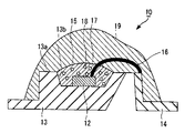
- FIG. 2 is a cross-sectional view schematically showing an example of the structure of the light emitting device 10 according to the embodiment of the present invention.
- the light emitting device 10 shown in FIG. 2 includes an LED chip as the light emitting source 12, a first lead frame 13 on which the light emitting source 12 is mounted, a second lead frame 14, and a wavelength conversion member 15 that covers the light emitting source 12. And a bonding wire 16 that electrically connects the light emitting source 12 and the second lead frame 14, and a synthetic resin cap 19 that covers them.
- the wavelength conversion member 15 has a phosphor 18 and a sealing resin 17 in which the phosphor 18 is dispersed.
- a recess 13b for mounting a light emitting diode chip as the light emitting source 12 is formed on the upper portion 13a of the first lead frame 13.
- the recess 13b has a substantially funnel shape in which the hole diameter gradually increases upward from the bottom surface, and the inner surface of the recess 13b serves as a reflecting surface.
- An electrode on the lower surface side of the light emitting source 12 is die-bonded to the bottom surface of the reflecting surface.
- the other electrode formed on the upper surface of the light emitting source 12 is connected to the surface of the second lead frame 14 via the bonding wire 16.
- LED chips can be used as the light emitting source 12. Particularly preferred is an LED chip that emits light having a wavelength of near-ultraviolet to blue light of 300 nm to 500 nm.
- the phosphor 18 used for the wavelength conversion member 15 of the light emitting device 10 includes the ⁇ -sialon phosphor according to the present embodiment. Further, from the viewpoint of controlling the light wavelength control of the light emitting device 10, the phosphor 18 includes ⁇ -sialon phosphor, KSF-based phosphor, CaAlSiN 3 , and YAG in addition to the ⁇ -sialon phosphor according to the present embodiment. A phosphor such as a single substance or a mixture may be further included. Examples of elements that are solid-dissolved in these phosphors include europium (Eu), cerium (Ce), strontium (Sr), calcium (Ca), manganese (Mn), and the like.
- these phosphors may be used alone or in combination of two or more.
- the KSF-based phosphor in which manganese is dissolved is preferable.
- the ⁇ -sialon phosphor according to the present embodiment showing a green color and the KSF-based phosphor showing a red color in combination for example, it can be suitably used as a backlight LED suitable for a high color rendering TV or the like. it can.
- the light emitting source 12 and the wavelength conversion member 15 it is possible to emit light having high emission intensity.
- the emission light source 12 by irradiating the emission light source 12 with near-ultraviolet light or visible light having a wavelength of 300 nm or more and 500 nm or less as an excitation source. It has a green emission characteristic having a peak in a wavelength range of 520 nm to 550 nm.
- a near-ultraviolet LED chip or a blue LED chip and the ⁇ -sialon phosphor according to the present embodiment are used as the light emitting source 12, and the red light emitting phosphor, the blue light emitting phosphor, and the yellow light having a wavelength of 600 nm or more and 700 nm or less are used.
- White light can be obtained by combining the light emitting phosphor or the orange light emitting phosphor alone or in a mixture.
- the light emitting device 10 of the present invention includes the ⁇ -sialon phosphor with improved emission intensity, it is possible to improve the brightness.
- a reference mode of the present invention is additionally described below.
- a ⁇ -sialon phosphor in which europium is dissolved The 50% area average diameter of primary particles of the ⁇ -sialon phosphor is defined as D 50 , When the 10% area average diameter of the primary particles of the ⁇ -sialon phosphor is D 10 , The above D 50 is 7.0 ⁇ m or more and 20.0 ⁇ m or less, A ⁇ -sialon phosphor having (D 50 ⁇ D 10 ) / D 50 of 0.60 or less.
- Example 1 Using a V-type mixer (S-3 manufactured by Tsutsui Rikagaku Kikai Co., Ltd.), 95.80% by mass of ⁇ -type silicon nitride powder (SN-E10 grade, oxygen content 1.0% by mass) manufactured by Ube Industries, Tokuyama Aluminum nitride powder (F grade, oxygen content 0.8% by mass) 2.74% by mass, aluminum oxide powder (TM-DAR grade) 0.56% by mass manufactured by Daimei Kagaku and manufactured by Shin-Etsu Chemical Co., Ltd.
- V-type mixer S-3 manufactured by Tsutsui Rikagaku Kikai Co., Ltd.
- 200 g of the obtained raw material powder having the first composition was filled in a cylindrical boron nitride container having an inner diameter of 10 cm and a height of 10 cm and having a lid, and was heated in an electric furnace of a carbon heater in a pressurized nitrogen atmosphere of 0.8 MPa at 1950.
- a heat treatment (first firing step) was performed at 10 ° C. for 10 hours.
- the heat-treated powder was pulverized by a supersonic jet pulverizer (PJM-80SP, manufactured by Nippon Pneumatic Mfg. Co., Ltd.), and then the obtained pulverized product was passed through a nylon sieve having an opening of 45 ⁇ m, One calcined powder was obtained.
- JM-80SP supersonic jet pulverizer
- the obtained first baked powder and the europium oxide powder (RU grade) manufactured by Shin-Etsu Chemical Co., Ltd. were mixed at a compounding ratio of 90:10 (referred to as a second compounding composition (mass%)), and V-shaped.
- the first calcined powder and europium oxide powder were mixed using a mixer (S-3, manufactured by Tsutsui Rikagaku Kikai Co., Ltd.).
- the obtained mixture was passed through a nylon sieve having openings of 250 ⁇ m to remove agglomerates to obtain a second raw material mixed powder.
- 200 g of the obtained raw material powder having the second blended composition was filled in a cylindrical boron nitride container with an inner diameter of 10 cm and a height of 10 cm and having a lid, and was placed in a carbon heater electric furnace in a pressurized nitrogen atmosphere of 0.8 MPa at 2020.
- a heat treatment (second firing step) was performed at 12 ° C. for 12 hours.
- the heat-treated powder was pulverized by a supersonic jet pulverizer (PJM-80SP, manufactured by Nippon Pneumatic Mfg. Co., Ltd.), and the obtained pulverized product was passed through a nylon sieve having an opening of 45 ⁇ m, Two calcined powders were obtained. The passing rate through the sieve was 92%.
- 20 g of the obtained second baked powder was filled in a cylindrical boron nitride container with a lid having an inner diameter of 5 cm and a height of 3.5 cm, and annealed at 1500 ° C. for 8 hours in an argon atmosphere in a carbon heater electric furnace. Processed. The annealed powder was subjected to an acid treatment of immersion in a 1: 1 mixed acid of 50% hydrofluoric acid and 70% nitric acid at 75 ° C. for 30 minutes.
- Example 1 Precipitate the powder after the acid treatment as it is, and repeat decantation to remove the supernatant and fine powder until the pH of the solution is 5 or more and the supernatant becomes transparent, and the finally obtained precipitate is filtered and dried,
- the phosphor powder of Example 1 was obtained.
- the crystal phase present was a ⁇ -sialon single phase, and a ⁇ -sialon phosphor was obtained.
- the Eu content measured by ICP emission spectroscopy was 0.72% by mass.
- Table 1 shows the first composition and the second composition in Example 1.
- EBSD method measurement is performed by using a scanning electron microscope (FE-SEM manufactured by JEOL Ltd., JSM-7001F type) 2 with an electron backscattering diffraction image measuring device (OIM device manufactured by EDAX-TSL) 3 added. did.
- the ⁇ -sialon phosphor of Example 1 is irradiated with an electron beam to generate scattering corresponding to the crystal structure and crystal orientation, and the shape of this scattering pattern is determined by software (EDAX-TSL). OIM, Ver. 5.2) was used to identify the crystal orientation in the particles of each phosphor. Further, the particle shape in each crystal orientation was subjected to image analysis, and from the above formulas (1), (2) and (3), 50% area average diameter D 50 of primary particles, 10% area average diameter D 10 and 90% were obtained. The area average diameter D 90 was calculated. Furthermore, the average number of primary particles in the secondary particles (ratio of the number of primary particles to the number of secondary particles of ⁇ -sialon) was calculated from the obtained image.
- the EBSD image of FIG. 4 was obtained from the ⁇ -sialon phosphor of Example 1 shown in the scanning electron microscope image of FIG. 3 (SEM image, electron acceleration voltage is 15 kV, magnification is 500 times). It was done by making.
- parts other than the black background are primary particles, and the lines shown inside each contour indicate the boundaries of primary particles having different directions. The statistical analysis accuracy improves as the number of primary particles increases. If the number of primary particles is 3000 or more, sufficient data can be obtained for analysis.
- ⁇ D V50 (50% volume average diameter)> The particle size distribution of the ⁇ -sialon phosphor of Example 1 was measured by a laser diffraction / scattering method, and D V50 was determined.
- the fluorescence characteristics of the ⁇ -sialon phosphor were evaluated by the peak intensity and peak wavelength measured by the following method.
- a spectrofluorometer (F-7000 manufactured by Hitachi High-Technologies Corporation) calibrated by the Rhodamine B method and a standard light source was used as the apparatus.
- the obtained phosphor powder was filled in a dedicated solid sample holder, and then, using a spectrofluorometer, a fluorescence spectrum when irradiated with excitation light having a wavelength of 455 nm was measured, and from the obtained fluorescence spectrum, The peak intensity and peak wavelength were determined.
- Table 2 The obtained results are shown in Table 2.
- the unit is an arbitrary unit because the peak intensity changes depending on the measuring device and conditions, and is measured under the same conditions in each Example and Comparative Example, and the ⁇ -sialon phosphors of each Example and Comparative Example are continuously measured. Then, a comparison was made. Table 2 shows the peak intensity of each phosphor when the peak intensity of the ⁇ -sialon phosphor of Comparative Example 1 is 100%.
- CIE chromaticity The CIE (Commission Internationale de l'Eclairage) chromaticity of the fluorescence spectrum is measured by an instantaneous multimetering system (MCPD-7000, manufactured by Otsuka Electronics Co., Ltd.) using an integrating sphere to collect fluorescence for excitation at 455 nm. It was determined by measuring the emission spectrum of the total luminous flux emitted.
- MCPD-7000 instantaneous multimetering system
- Examples 2 and 3 ⁇ -Sialon phosphor powders were obtained in the same manner as in Example 1 except that the second composition was changed to the composition ratio shown in Table 1.
- the crystal phase present in each was a ⁇ -sialon single phase.
- the same evaluation as in Example 1 was performed. The obtained results are shown in Table 1 and Table 2, respectively.
- Example 1 A ⁇ -sialon phosphor powder was obtained in the same manner as in Example 1 except that the step corresponding to the second firing step in Example 1 was not performed. As a result of powder X-ray diffraction measurement performed on the obtained ⁇ -sialon phosphor, the crystal phase present was a ⁇ -sialon single phase. Moreover, the same evaluation as in Example 1 was performed. The obtained results are shown in Table 1 and Table 2, respectively.
- Example 4 In the first firing step of Example 2, the same method as in Example 2 except that 5% by mass of the first fired powder of Example 2 was added and the first composition was changed to the composition ratio shown in Table 1. Thus, ⁇ -sialon phosphor powder was obtained. Moreover, the same evaluation as in Example 1 was performed. The obtained results are shown in Table 1 and Table 2, respectively.
- Example 2 A ⁇ -sialon phosphor powder was obtained in the same manner as in Example 4 except that the step corresponding to the second firing step in Example 4 was not performed. As a result of powder X-ray diffraction measurement performed on the obtained ⁇ -sialon phosphor, the crystal phase present was a ⁇ -sialon single phase. Moreover, the same evaluation as in Example 1 was performed. The obtained results are shown in Table 1 and Table 2, respectively.
- Example 5 A ⁇ -sialon phosphor powder was obtained in the same manner as in Example 2, except that the pulverization conditions were adjusted so that the particle size was smaller. Moreover, the same evaluation as in Example 1 was performed. The obtained results are shown in Table 1 and Table 2, respectively.
- Example 3 A ⁇ -sialon phosphor powder was obtained in the same manner as in Example 5, except that the step corresponding to the second firing step in Example 5 was not performed. As a result of powder X-ray diffraction measurement performed on the obtained ⁇ -sialon phosphor, the crystal phase present was a ⁇ -sialon single phase. Moreover, the same evaluation as in Example 1 was performed. The obtained results are shown in Table 1 and Table 2, respectively.
- the ⁇ -sialon phosphors of Examples 1 to 5 are ⁇ -sialon phosphors having higher fluorescence peak intensity and higher brightness than the ⁇ -sialon phosphors of Comparative Examples 1 to 3. Do you get it.
Landscapes
- Chemical & Material Sciences (AREA)
- Inorganic Chemistry (AREA)
- Engineering & Computer Science (AREA)
- Materials Engineering (AREA)
- Organic Chemistry (AREA)
- Luminescent Compositions (AREA)
Abstract
ユウロピウムが固溶したβ型サイアロン蛍光体であって、上記β型サイアロン蛍光体の一次粒子の50%面積平均径をD50とし、上記β型サイアロン蛍光体の一次粒子の10%面積平均径をD10としたとき、上記D50が7.0μm以上20.0μm以下であり、(D50-D10)/D50が0.60以下であるβ型サイアロン蛍光体。ここで、一次粒子とは、β型サイアロン蛍光体の個々の粒子における結晶方位を電子後方散乱回折像法により識別して結晶方位毎に区別した単結晶粒子と定義される。そして、D50およびD10は、その一次粒子の断面積を画像解析することで求められる。
Description
本発明は、β型サイアロン蛍光体および発光装置に関する。
一次光を発する発光素子と、一次光を吸収して二次光を発する蛍光体とを組み合わせた発光装置が知られている。
近年、発光装置の高出力化に伴い、蛍光体の耐熱性および耐久性に対する要求が高まっており、結晶構造が安定したβ型サイアロン蛍光体が注目されている。
近年、発光装置の高出力化に伴い、蛍光体の耐熱性および耐久性に対する要求が高まっており、結晶構造が安定したβ型サイアロン蛍光体が注目されている。
β型サイアロンの結晶構造内にEu2+を固溶させた蛍光体は、紫外から青色の光で励起され520~550nmの緑色発光を示す蛍光体である。Eu2+を固溶させたβ型サイアロンは、Eu固溶β型サイアロンとも呼ばれる。この蛍光体は、白色発光ダイオード(白色LED(Light Emitting Diode)と呼ぶ。)等の発光装置の緑色発光成分として使用されている。Eu固溶β型サイアロンは、Eu2+を固溶させた蛍光体の中でも、発光スペクトルは非常にシャープであり、特に青、緑、赤の光の3原色からなる狭帯域発光が要求される液晶ディスプレイパネルのバックライト光源の緑色発光成分に好適な蛍光体である。
このようなβ型サイアロン蛍光体に関する技術としては、例えば、以下の特許文献1に記載のものが挙げられる。
特許文献1(国際公開第2012/011444号)には、一般式:Si6-ZAlZOZN8-Z(0<Z≦0.42)で示され、Euを固溶させたβ型サイアロンであって、β型サイアロンの一次粒子の50%面積平均径が5μm以上であるβ型サイアロンが記載されている。
β型サイアロン蛍光体および発光装置については、輝度のさらなる向上が求められている。
本発明は上記事情に鑑みてなされたものである。本発明は、輝度が向上したβ型サイアロン蛍光体および発光装置を提供するものである。
本発明者らは、輝度が向上したβ型サイアロン蛍光体および発光装置を提供するために鋭意検討を重ねた。その結果、以下で説明されるD50および(D50-D10)/D50をそれぞれ特定の範囲にすると、β型サイアロン蛍光体およびそれを用いた発光装置の輝度を向上できることを見出し、本発明に至った。
すなわち、本発明によれば、以下に示すβ型サイアロン蛍光体および発光装置が提供される。
1.
ユウロピウムが固溶したβ型サイアロン蛍光体であって、
前記β型サイアロン蛍光体の個々の粒子における結晶方位を電子後方散乱回折像法により識別して結晶方位毎に区別した単結晶粒子を一次粒子と定義したとき、
前記一次粒子の断面積を画像解析により求めたときの、
前記β型サイアロン蛍光体の前記一次粒子の50%面積平均径をD50とし、
前記β型サイアロン蛍光体の前記一次粒子の10%面積平均径をD10としたとき、
D50が7.0μm以上20.0μm以下であり、
(D50-D10)/D50が0.60以下であるβ型サイアロン蛍光体。
2.
1.に記載のβ型サイアロン蛍光体において、
前記β型サイアロン蛍光体の前記一次粒子の90%面積平均径をD90としたとき、
(D90-D10)/D50が1.45以下であるβ型サイアロン蛍光体。
3.
1.または2.に記載のβ型サイアロン蛍光体において、
一般式Si6-zAlzOzN8-z:Eu2+(0<Z≦4.2)で示されるβ型サイアロン蛍光体。
4.
1.乃至3.のいずれか一つに記載のβ型サイアロン蛍光体において、
前記β型サイアロン蛍光体のDV50粒径(JIS R1629:1997に準拠したレーザー回折散乱法による体積基準の積算分率における50%径)が5μm以上50μm以下であるβ型サイアロン蛍光体。
5.
1.乃至4.のいずれか一つに記載のβ型サイアロン蛍光体において、
複数の前記一次粒子同士が粒界を介して焼結した粒子を二次粒子と定義したとき、
前記β型サイアロン蛍光体の前記二次粒子数に対する前記一次粒子数の比が1.90以下であるβ型サイアロン蛍光体。
6.
発光光源と波長変換部材とを含む発光装置であって、
前記波長変換部材は蛍光体を含み、
前記蛍光体が1.乃至5.のいずれか一つに記載のβ型サイアロン蛍光体を含む発光装置。
7.
6.に記載の発光装置において、
前記発光光源が、300nm~500nmの波長の光を発生するLEDチップを含む発光装置。
8.
6.または7.に記載の発光装置において、
前記蛍光体が、マンガンが固溶したKSF系蛍光体をさらに含む発光装置。
ユウロピウムが固溶したβ型サイアロン蛍光体であって、
前記β型サイアロン蛍光体の個々の粒子における結晶方位を電子後方散乱回折像法により識別して結晶方位毎に区別した単結晶粒子を一次粒子と定義したとき、
前記一次粒子の断面積を画像解析により求めたときの、
前記β型サイアロン蛍光体の前記一次粒子の50%面積平均径をD50とし、
前記β型サイアロン蛍光体の前記一次粒子の10%面積平均径をD10としたとき、
D50が7.0μm以上20.0μm以下であり、
(D50-D10)/D50が0.60以下であるβ型サイアロン蛍光体。
2.
1.に記載のβ型サイアロン蛍光体において、
前記β型サイアロン蛍光体の前記一次粒子の90%面積平均径をD90としたとき、
(D90-D10)/D50が1.45以下であるβ型サイアロン蛍光体。
3.
1.または2.に記載のβ型サイアロン蛍光体において、
一般式Si6-zAlzOzN8-z:Eu2+(0<Z≦4.2)で示されるβ型サイアロン蛍光体。
4.
1.乃至3.のいずれか一つに記載のβ型サイアロン蛍光体において、
前記β型サイアロン蛍光体のDV50粒径(JIS R1629:1997に準拠したレーザー回折散乱法による体積基準の積算分率における50%径)が5μm以上50μm以下であるβ型サイアロン蛍光体。
5.
1.乃至4.のいずれか一つに記載のβ型サイアロン蛍光体において、
複数の前記一次粒子同士が粒界を介して焼結した粒子を二次粒子と定義したとき、
前記β型サイアロン蛍光体の前記二次粒子数に対する前記一次粒子数の比が1.90以下であるβ型サイアロン蛍光体。
6.
発光光源と波長変換部材とを含む発光装置であって、
前記波長変換部材は蛍光体を含み、
前記蛍光体が1.乃至5.のいずれか一つに記載のβ型サイアロン蛍光体を含む発光装置。
7.
6.に記載の発光装置において、
前記発光光源が、300nm~500nmの波長の光を発生するLEDチップを含む発光装置。
8.
6.または7.に記載の発光装置において、
前記蛍光体が、マンガンが固溶したKSF系蛍光体をさらに含む発光装置。
本発明によれば、輝度が向上したβ型サイアロン蛍光体および発光装置を提供することができる。
上述した目的、およびその他の目的、特徴および利点は、以下に述べる好適な実施の形態、およびそれに付随する以下の図面によってさらに明らかになる。
以下、本発明の実施の形態について、図面を用いて説明するが、本発明はこれらに限定されて解釈されるべきものではなく、本発明の要旨を逸脱しない限りにおいて、当業者の知識に基づいて、種々の変更、改良等を行うことができる。実施形態に開示されている複数の構成要素は、適宜な組み合わせにより、種々の発明を形成できる。例えば、実施形態に示される全構成要素からいくつかの構成要素を削除してもよいし、異なる実施形態の構成要素を適宜組み合わせてもよい。
図は概略図であり、実際の寸法比率とは必ずしも一致していない。
数値範囲の「A~B」は、特に断りがなければ、A以上B以下を表す。
図は概略図であり、実際の寸法比率とは必ずしも一致していない。
数値範囲の「A~B」は、特に断りがなければ、A以上B以下を表す。
(β型サイアロン蛍光体)
本実施形態に係るβ型サイアロン蛍光体は、ユウロピウムが固溶したβ型サイアロン蛍光体であって、上記β型サイアロン蛍光体の一次粒子の50%面積平均径をD50とし、上記β型サイアロン蛍光体の一次粒子の10%面積平均径をD10としたとき、上記D50が7.0μm以上20.0μm以下であり、(D50-D10)/D50が0.60以下である。
ここで、「一次粒子」とは、β型サイアロン蛍光体の個々の粒子における結晶方位を電子後方散乱回折像法により識別して結晶方位毎に区別した単結晶粒子と定義される。また、D50およびD10は、その一次粒子の断面積を画像解析することで求められる。具体的な測定方法などは後述する。
本実施形態に係るβ型サイアロン蛍光体は、ユウロピウムが固溶したβ型サイアロン蛍光体であって、上記β型サイアロン蛍光体の一次粒子の50%面積平均径をD50とし、上記β型サイアロン蛍光体の一次粒子の10%面積平均径をD10としたとき、上記D50が7.0μm以上20.0μm以下であり、(D50-D10)/D50が0.60以下である。
ここで、「一次粒子」とは、β型サイアロン蛍光体の個々の粒子における結晶方位を電子後方散乱回折像法により識別して結晶方位毎に区別した単結晶粒子と定義される。また、D50およびD10は、その一次粒子の断面積を画像解析することで求められる。具体的な測定方法などは後述する。
本実施形態に係るβ型サイアロン蛍光体は、例えば、一般式Si6-zAlzOzN8-z:Eu2+(0<Z≦4.2)で示され、Eu2+を固溶させたβ型サイアロンからなる蛍光体である。以下、ユウロピウムが固溶したβ型サイアロンを単にβ型サイアロンともいう。
一般式Si6-zAlzOzN8-z:Eu2+において、Z値とユウロピウムの含有量は特に限定されないが、Z値は、例えば0を超えて4.2以下であり、β型サイアロン蛍光体の発光強度をより向上させる観点から、好ましくは0.005以上1.0以下である。またユウロピウムの含有量は0.1質量%以上2.0質量%以下であることが好ましい。
β型サイアロン蛍光体は、複数の粒子が焼成工程での加熱処理時に強固に一体化されたものであり、複数の粒子の各一粒を一次粒子、複数の粒子が強固に一体化されたものを二次粒子と呼んでいる。より具体的には、一次粒子とは、前述のように、β型サイアロン蛍光体の個々の粒子における結晶方位を電子後方散乱回折像法により識別して結晶方位毎に区別した単結晶粒子と定義することができる。また、二次粒子とは、複数の一次粒子同士が粒界を介して焼結した粒子と定義することができる。
本実施形態に係るβ型サイアロン蛍光体によれば、β型サイアロン蛍光体の一次粒子のD50および(D50-D10)/D50が上記範囲内であると、発光強度すなわち輝度を向上させることができる。
この理由については必ずしも明らかではないが、以下の理由が推察される。
β型サイアロン蛍光体の一次粒子の粒子径が大きいと、結晶粒界に存在する不純物の割合が低下して結晶性が向上するため、発光効率を向上させることができると考えられる。そのため、β型サイアロン蛍光体の一次粒子のD50および(D50-D10)/D50が上記範囲内であると、一次粒子の粒子径が小さく発光効率が低いβ型サイアロン粒子の割合が相対的に少なくなり、一次粒子の粒子径が大きく発光効率が高いβ型サイアロン粒子の割合が相対的に多くなる。その結果、β型サイアロン蛍光体の発光強度を向上させることができると考えられる。
以上の理由から、本実施形態によれば、輝度が向上したβ型サイアロン蛍光体および発光装置を提供することができる。
本実施形態において、β型サイアロン蛍光体の一次粒子のD50および(D50-D10)/D50は、後述するように、β型サイアロン蛍光体の原料の一つであるユウロピウム化合物を2回以上に分けて添加して焼成工程をおこなうとともに、2回目の焼成工程において従来よりもユウロピウム化合物を多量に添加して製造すること等によって実現することが可能である。
この理由については必ずしも明らかではないが、以下の理由が推察される。
β型サイアロン蛍光体の一次粒子の粒子径が大きいと、結晶粒界に存在する不純物の割合が低下して結晶性が向上するため、発光効率を向上させることができると考えられる。そのため、β型サイアロン蛍光体の一次粒子のD50および(D50-D10)/D50が上記範囲内であると、一次粒子の粒子径が小さく発光効率が低いβ型サイアロン粒子の割合が相対的に少なくなり、一次粒子の粒子径が大きく発光効率が高いβ型サイアロン粒子の割合が相対的に多くなる。その結果、β型サイアロン蛍光体の発光強度を向上させることができると考えられる。
以上の理由から、本実施形態によれば、輝度が向上したβ型サイアロン蛍光体および発光装置を提供することができる。
本実施形態において、β型サイアロン蛍光体の一次粒子のD50および(D50-D10)/D50は、後述するように、β型サイアロン蛍光体の原料の一つであるユウロピウム化合物を2回以上に分けて添加して焼成工程をおこなうとともに、2回目の焼成工程において従来よりもユウロピウム化合物を多量に添加して製造すること等によって実現することが可能である。
本実施形態に係るβ型サイアロン蛍光体の一次粒子の50%面積平均径をD50は7.0μm以上20.0μm以下であるが、好ましくは9.0μm以上であり、そして好ましくは18.0μm以下、より好ましくは15.0μm以下である。
また、(D50-D10)/D50が0.60以下であるが、好ましくは0.55以下であり、より好ましくは0.53以下であり、さらに好ましくは0.51以下である。これにより、β型サイアロン粒子間の特性の差を小さくすることができる。その結果、得られる発光装置の発光特性や色のバラツキを低減することができる。
また、(D50-D10)/D50が0.60以下であるが、好ましくは0.55以下であり、より好ましくは0.53以下であり、さらに好ましくは0.51以下である。これにより、β型サイアロン粒子間の特性の差を小さくすることができる。その結果、得られる発光装置の発光特性や色のバラツキを低減することができる。
本実施形態に係るβ型サイアロン蛍光体において、β型サイアロン蛍光体の発光強度をさらに向上させる観点から、β型サイアロン蛍光体の一次粒子の90%面積平均径をD90としたとき、(D90-D10)/D50が1.45以下であることが好ましく、1.35以下であることがより好ましい。また、(D90-D10)/D50が上記上限値以下であると、β型サイアロン粒子間の特性の差を小さくすることができる。その結果、得られる発光装置の発光特性や色のバラツキを低減することができる。
一次粒子の50%面積平均径D50、10%面積平均径D10および90%面積平均径D90についてより具体的に説明する。
β型サイアロン蛍光体の個々の一次粒子、すなわち単結晶粒子が、断面積の小さな順から、CA1,CA2,CA3,・・・,CAi,・・・,CAkのように並べられる一次粒子の集団があるとする。ここで言う一次粒子とは、全ての単結晶粒子を意味し、複数の一次粒子同士が粒界を介して焼結して二次粒子を構成しているものと、二次粒子を構成していないものとを区別することなく含む。この一次粒子の集団の断面積の合計(CA1+CA2+CA3+・・・+CAi+・・・+CAk)を100%として累積カーブを求めたとき、この累積カーブの50%、10%および90%にあたる点の一次粒子の断面積(S50、S10、S90)より計算した一次粒子径を、それぞれ一次粒子の50%面積平均径D50、90%面積平均径D90および10%面積平均径D10とする。
β型サイアロン蛍光体の個々の一次粒子、すなわち単結晶粒子が、断面積の小さな順から、CA1,CA2,CA3,・・・,CAi,・・・,CAkのように並べられる一次粒子の集団があるとする。ここで言う一次粒子とは、全ての単結晶粒子を意味し、複数の一次粒子同士が粒界を介して焼結して二次粒子を構成しているものと、二次粒子を構成していないものとを区別することなく含む。この一次粒子の集団の断面積の合計(CA1+CA2+CA3+・・・+CAi+・・・+CAk)を100%として累積カーブを求めたとき、この累積カーブの50%、10%および90%にあたる点の一次粒子の断面積(S50、S10、S90)より計算した一次粒子径を、それぞれ一次粒子の50%面積平均径D50、90%面積平均径D90および10%面積平均径D10とする。
一次粒子の50%面積平均径D50、10%面積平均径D10および90%面積平均径D90を求めるための具体的な方法について説明する。面積平均径を求めるには、一次粒子の断面積を測定し、累積カーブを作成する必要がある。
粒子の断面積は、電子後方散乱回折像法(Electron backscatter diffraction法、以下、EBSD法ともいう。)を利用して測定することができる。
図1は、EBSD法の測定に用いる装置の構成を示す模式図である。
図1に示すように、EBSD法に用いる装置1は、走査型電子顕微鏡2に電子後方散乱回折像法測定装置3を付加した装置から構成されている。走査型電子顕微鏡2は、鏡筒部2A、試料4が載置されるステージ部2B、ステージ制御部2C、電子線走査部2D、制御用コンピュータ2E等から構成されている。電子後方散乱回折像法測定装置3は、試料4に電子線5が照射されて発生し後方へ散乱された電子6を検出する蛍光スクリーン7と、この蛍光スクリーン7の蛍光画像を撮像するカメラ8と、図示しない電子後方散乱回折像のデータの取得及び解析を行うソフトウエア等から構成されている。
粒子の断面積は、電子後方散乱回折像法(Electron backscatter diffraction法、以下、EBSD法ともいう。)を利用して測定することができる。
図1は、EBSD法の測定に用いる装置の構成を示す模式図である。
図1に示すように、EBSD法に用いる装置1は、走査型電子顕微鏡2に電子後方散乱回折像法測定装置3を付加した装置から構成されている。走査型電子顕微鏡2は、鏡筒部2A、試料4が載置されるステージ部2B、ステージ制御部2C、電子線走査部2D、制御用コンピュータ2E等から構成されている。電子後方散乱回折像法測定装置3は、試料4に電子線5が照射されて発生し後方へ散乱された電子6を検出する蛍光スクリーン7と、この蛍光スクリーン7の蛍光画像を撮像するカメラ8と、図示しない電子後方散乱回折像のデータの取得及び解析を行うソフトウエア等から構成されている。
この装置を用いて、試料4であるβ型サイアロン蛍光体に電子線を照射して結晶構造と結晶面に対応した電子散乱を生じさせ、この電子散乱のパターンの形状を、ソフトウエアにより解析する。より具体的には、個々の蛍光体の粒子における結晶方位を識別し、個々の結晶方位毎に区別できる一次粒子の断面積を画像解析により求める。 次いで、得られた断面積から、上記のように累積カーブを作成し、50%、10%および90%にあたる点の一次粒子の断面積(S50、S10、S90)を求め、これらを用いて、下記式(1)、(2)および式(3)から、円換算した場合の直径にあたる一次粒子の50%面積平均径D50、10%面積平均径D10および90%面積平均径D90をそれぞれ算出する。
一次粒子の50%面積平均径=2×(S50/π)1/2 (1)
式中、S50は、個々の一次粒子の面積の累積カーブが50%となる点の一次粒子の面積である。
一次粒子の10%面積平均径=2×(S10/π)1/2 (2)
式中、S10は、個々の一次粒子の面積の累積カーブが10%となる点の一次粒子の面積である。
一次粒子の90%面積平均径=2×(S90/π)1/2 (3)
式中、S90は、個々の一次粒子の面積の累積カーブが90%となる点の一次粒子の面積である。
一次粒子の50%面積平均径=2×(S50/π)1/2 (1)
式中、S50は、個々の一次粒子の面積の累積カーブが50%となる点の一次粒子の面積である。
一次粒子の10%面積平均径=2×(S10/π)1/2 (2)
式中、S10は、個々の一次粒子の面積の累積カーブが10%となる点の一次粒子の面積である。
一次粒子の90%面積平均径=2×(S90/π)1/2 (3)
式中、S90は、個々の一次粒子の面積の累積カーブが90%となる点の一次粒子の面積である。
樹脂中の分散状態を向上させ、β型サイアロン蛍光体を用いて作製されるLED等の発光装置の色バラツキや輝度の低下を抑制する観点から、本実施形態に係るβ型サイアロン蛍光体のDV50粒径(50%体積平均径)は50μm以下であることが好ましく、40μm以下であることがより好ましく、30μm以下がさらに好ましい。
また、本実施形態に係るβ型サイアロン蛍光体のDV50粒径(50%体積平均径)は5μm以上であることが好ましく、10μm以上であることがより好ましい。これにより、β型サイアロン蛍光体の発光効率を向上させたり、光の散乱を抑制して輝度を向上させたりすることができる。
ここで、本実施形態において「DV50粒径(50%体積平均径)」とは、JIS R1629:1997に準拠したレーザー回折散乱法による体積基準の積算分率における50%径を意味する。DV50粒径(50%体積平均径)の定義および測定法は、D50、D10およびD90の定義および測定法とは異なることに留意されたい。
また、本実施形態に係るβ型サイアロン蛍光体のDV50粒径(50%体積平均径)は5μm以上であることが好ましく、10μm以上であることがより好ましい。これにより、β型サイアロン蛍光体の発光効率を向上させたり、光の散乱を抑制して輝度を向上させたりすることができる。
ここで、本実施形態において「DV50粒径(50%体積平均径)」とは、JIS R1629:1997に準拠したレーザー回折散乱法による体積基準の積算分率における50%径を意味する。DV50粒径(50%体積平均径)の定義および測定法は、D50、D10およびD90の定義および測定法とは異なることに留意されたい。
また、β型サイアロン蛍光体の二次粒子中における一次粒子の平均個数が少ないほど、発光効率は大きくなる。このβ型サイアロン蛍光体の二次粒子数に対する一次粒子数の比の二次粒子数に対する一次粒子数の比は、EBSD法により得られたβ型サイアロンの画像内の二次粒子の個数と、二次粒子を構成する一次粒子の個数とを数え、二次粒子数に対する一次粒子数の比を取ることによって算出する。β型サイアロン蛍光体の二次粒子数に対する一次粒子数の比すなわち二次粒子中における一次粒子の平均個数は、1.90以下であることが好ましく、1.80以下であることがより好ましく、1.70以下であることがさらに好ましく、1.60以下であることがよりさらに好ましい。
また、β型サイアロン蛍光体の二次粒子数に対する一次粒子数の比が上記上限値以下であると、β型サイアロン粒子間の特性の差を小さくすることができ、その結果、得られる発光装置の発光特性や色のバラツキを低減することができる。
また、β型サイアロン蛍光体の二次粒子数に対する一次粒子数の比が上記上限値以下であると、β型サイアロン粒子間の特性の差を小さくすることができ、その結果、得られる発光装置の発光特性や色のバラツキを低減することができる。
本実施形態に係るβ型サイアロンは、紫外線から可視光の幅広い波長域で励起され、高効率で520nm以上550nm以下の範囲内を主波長とした緑色の発光をする。よって、緑色発光の蛍光体として優れている。
また、本実施形態に係るβ型サイアロン蛍光体は、発光素子における蛍光体層の材料として好適に用いることができる。発光素子は、ディスプレイのバックライト光源、照明装置等の発光装置に適用することができる。発光素子としては、特に限定されないが、例えば、LEDと、LEDの発光面側に積層された蛍光体層とを備える。LEDとしては、300~500nmの波長の光を発する紫外LEDまたは青色LED、特に440~480nmの波長の光を発する青色LEDを用いることができる。特に、本実施形態に係る製造方法によって得られたβ型サイアロン蛍光体は、紫外から青色光の幅広い波長で励起され、高輝度の緑色発光を示すことから、青色または紫外光を光源とする白色LEDの蛍光体として好適に使用できる。
また、本実施形態に係るβ型サイアロン蛍光体は、発光素子における蛍光体層の材料として好適に用いることができる。発光素子は、ディスプレイのバックライト光源、照明装置等の発光装置に適用することができる。発光素子としては、特に限定されないが、例えば、LEDと、LEDの発光面側に積層された蛍光体層とを備える。LEDとしては、300~500nmの波長の光を発する紫外LEDまたは青色LED、特に440~480nmの波長の光を発する青色LEDを用いることができる。特に、本実施形態に係る製造方法によって得られたβ型サイアロン蛍光体は、紫外から青色光の幅広い波長で励起され、高輝度の緑色発光を示すことから、青色または紫外光を光源とする白色LEDの蛍光体として好適に使用できる。
(β型サイアロン蛍光体の製造方法)
次に、本実施形態に係るβ型サイアロン蛍光体の製造方法について説明する。
本実施形態に係るβ型サイアロン蛍光体の製造方法は、従来のβ型サイアロン蛍光体の製造方法とは異なるものである。すなわち、一次粒子の50%面積平均径D50および(D50-D10)/D50が上記範囲内であるβ型サイアロン蛍光体は、β型サイアロン蛍光体の原料の一つであるユウロピウム化合物を2回以上に分けて添加して焼成工程をおこなうとともに、2回目の焼成工程において従来よりもユウロピウム化合物を多量に添加して製造するという製法上の工夫点を採用することによって初めて得ることができる。
ただし、本実施形態に係るβ型サイアロン蛍光体は、上記製法上の工夫点を採用することを前提に、例えば、その他の具体的な製造条件は種々のものを採用することができる。
次に、本実施形態に係るβ型サイアロン蛍光体の製造方法について説明する。
本実施形態に係るβ型サイアロン蛍光体の製造方法は、従来のβ型サイアロン蛍光体の製造方法とは異なるものである。すなわち、一次粒子の50%面積平均径D50および(D50-D10)/D50が上記範囲内であるβ型サイアロン蛍光体は、β型サイアロン蛍光体の原料の一つであるユウロピウム化合物を2回以上に分けて添加して焼成工程をおこなうとともに、2回目の焼成工程において従来よりもユウロピウム化合物を多量に添加して製造するという製法上の工夫点を採用することによって初めて得ることができる。
ただし、本実施形態に係るβ型サイアロン蛍光体は、上記製法上の工夫点を採用することを前提に、例えば、その他の具体的な製造条件は種々のものを採用することができる。
以下、本実施形態に係るβ型サイアロン蛍光体の製造方法をより具体的に説明する。
本実施形態に係るβ型サイアロン蛍光体の製造方法は、少なくとも以下の2つの焼成工程を含む。すなわち、本実施形態に係るβ型サイアロン蛍光体の製造方法は、第一ユウロピウム化合物を含む第一原料粉末を焼成して、β型サイアロン粒子を含む第一焼成粉を得る第一焼成工程と、得られた第一焼成粉および第二ユウロピウム化合物を含む第二原料粉末を焼成して、本実施形態に係るβ型サイアロン蛍光体を得る第二焼成工程と、を含む。
ここで、第二焼成工程において、第二ユウロピウム化合物を従来の基準よりも多く添加するようにする。より具体的には、第二焼成工程において、β型サイアロンに固溶可能なEu量よりもEu量が過剰になるように第二ユウロピウム化合物を添加する。
第二焼成工程において、β型サイアロンに固溶可能なEu量よりもEu量が過剰になるように第二ユウロピウム化合物を添加することによって、第二焼成工程におけるβ型サイアロン粒子の焼成時に液相を形成し、粒子径が小さいβ型サイアロン粒子の一次粒子をより粗大化できる。これにより、β型サイアロン蛍光体の一次粒子の50%面積平均径D50および(D50-D10)/D50を上記範囲内に調整することが可能となる。
本実施形態に係るβ型サイアロン蛍光体の製造方法は、少なくとも以下の2つの焼成工程を含む。すなわち、本実施形態に係るβ型サイアロン蛍光体の製造方法は、第一ユウロピウム化合物を含む第一原料粉末を焼成して、β型サイアロン粒子を含む第一焼成粉を得る第一焼成工程と、得られた第一焼成粉および第二ユウロピウム化合物を含む第二原料粉末を焼成して、本実施形態に係るβ型サイアロン蛍光体を得る第二焼成工程と、を含む。
ここで、第二焼成工程において、第二ユウロピウム化合物を従来の基準よりも多く添加するようにする。より具体的には、第二焼成工程において、β型サイアロンに固溶可能なEu量よりもEu量が過剰になるように第二ユウロピウム化合物を添加する。
第二焼成工程において、β型サイアロンに固溶可能なEu量よりもEu量が過剰になるように第二ユウロピウム化合物を添加することによって、第二焼成工程におけるβ型サイアロン粒子の焼成時に液相を形成し、粒子径が小さいβ型サイアロン粒子の一次粒子をより粗大化できる。これにより、β型サイアロン蛍光体の一次粒子の50%面積平均径D50および(D50-D10)/D50を上記範囲内に調整することが可能となる。
また、このβ型サイアロン蛍光体の製造方法は、第二焼成粉をさらに焼成して第三の焼成粉を得る第三の焼成工程を1回以上さらに含んでもよい。その際にさらにユウロピウム化合物を加えてもよい。
ここで、本実施形態において「第一焼成工程」とは、第一ユウロピウム化合物を含む原料粉末を熱処理する1回目の焼成工程のことを意味し、「第二焼成工程」とは、第二ユウロピウム化合物を添加して熱処理する2回目の焼成工程のことを意味し、「第三の焼成工程」とは、第二焼成工程以降に行う焼成工程のことを意味する。
また、本実施形態において「第一ユウロピウム化合物」とは第一焼成工程で添加されるユウロピウム化合物のことを意味し、「第二ユウロピウム化合物」とは第二焼成工程で添加されるユウロピウム化合物のことを意味する。
また、本実施形態において「第一原料粉末」とは第一焼成工程に用いる原料粉末のことを意味し、「第二原料粉末」とは第二焼成工程に用いる原料粉末のことである。それぞれの原料粉末は混合されていることが好ましい。
また、本実施形態において「第一焼成粉」とは第一焼成工程で得られる生成物のことを意味し、「第二焼成粉」とは第二焼成工程で得られる生成物のことを意味し、「第三の焼成粉」とは第三の焼成工程で得られる生成物のことを意味する。
また、本実施形態において「第一ユウロピウム化合物」とは第一焼成工程で添加されるユウロピウム化合物のことを意味し、「第二ユウロピウム化合物」とは第二焼成工程で添加されるユウロピウム化合物のことを意味する。
また、本実施形態において「第一原料粉末」とは第一焼成工程に用いる原料粉末のことを意味し、「第二原料粉末」とは第二焼成工程に用いる原料粉末のことである。それぞれの原料粉末は混合されていることが好ましい。
また、本実施形態において「第一焼成粉」とは第一焼成工程で得られる生成物のことを意味し、「第二焼成粉」とは第二焼成工程で得られる生成物のことを意味し、「第三の焼成粉」とは第三の焼成工程で得られる生成物のことを意味する。
また、本実施形態において、「工程」には、独立した工程だけではなく、他の工程と明確に区別できない場合であってもその工程の所期の目的が達成されれば、本用語に含まれる。
また、組成物中のユウロピウムの含有量は、組成物中にユウロピウムに該当する物質が複数存在する場合、特に断らない限り、組成物中に存在する当該複数の物質の合計量を意味する。
また、組成物中のユウロピウムの含有量は、組成物中にユウロピウムに該当する物質が複数存在する場合、特に断らない限り、組成物中に存在する当該複数の物質の合計量を意味する。
第一原料粉末は、第一ユウロピウム化合物に加えて、窒化ケイ素および窒化アルミニウムを含むことが好ましい。窒化ケイ素およびアルミニウム化合物はβ型サイアロンの骨格を形成するための材料であり、ユウロピウム化合物は発光中心を形成するための材料である。
また、第一原料粉末は、β型サイアロンをさらに含有してもよい。β型サイアロンは、骨材または核となる材料である。
第一原料粉末に含有される上記各成分の形態は、特に限定されないが、いずれも粉末状であることが好ましい。
また、第一原料粉末は、β型サイアロンをさらに含有してもよい。β型サイアロンは、骨材または核となる材料である。
第一原料粉末に含有される上記各成分の形態は、特に限定されないが、いずれも粉末状であることが好ましい。
ユウロピウム化合物としては、特に限定されないが、例えば、ユウロピウムを含む酸化物、ユウロピウムを含む水酸化物、ユウロピウムを含む窒化物、ユウロピウムを含む酸窒化物、ユウロピウムを含むハロゲン化物等を挙げることができる。これらは、単独でまたは2種以上を組み合わせて用いることができる。これらの中でも、酸化ユウロピウム、窒化ユウロピウムおよびフッ化ユウロピウムをそれぞれ単独で用いることが好ましく、酸化ユウロピウムを単独で用いることがより好ましい。
ユウロピウム化合物は、複数回の焼成工程の焼成前にそれぞれ分けて添加される。具体的には、ユウロピウム化合物は、第一焼成工程および第二焼成工程の焼成前にそれぞれ添加される。
それぞれの焼成工程において、ユウロピウムは、β型サイアロン中に固溶するもの、揮発するもの、異相成分として残存するものとに分けられる。ユウロピウムを含有した異相成分は酸処理等で除去することが可能であるが、あまりに多量に生成した場合、酸処理で不溶な成分が生成し、輝度が低下する。また、余分な光を吸収しない異相であれば、残存した状態でもよく、この異相にユウロピウムが含有されていてもよい。なお、複数回の焼成工程の焼成前にユウロピウム化合物を添加する場合、ユウロピウム化合物以外のβ型サイアロン蛍光体原料をユウロピウム化合物と共に添加してもよい。
本実施形態に係るβ型サイアロン蛍光体の製造方法において、第一焼成粉および第二ユウロピウム化合物の合計を100質量%としたとき、β型サイアロン蛍光体の輝度向上に寄与しないEuをより一層効果的に除去し、得られるβ型サイアロン蛍光体の輝度をより一層向上させる観点から、第二ユウロピウム化合物の割合は好ましくは1.0質量%以上、より好ましくは2.0質量%以上、さらに好ましくは3.0質量%以上であり、酸処理で不溶な異相成分の発生量を低下させ、得られるβ型サイアロン蛍光体の輝度をより一層向上させる観点から、第二ユウロピウム化合物の割合は好ましくは18.0質量%以下、より好ましくは17.0質量%以下、さらに好ましくは15.0質量%以下である。
また、本実施形態に係るβ型サイアロン蛍光体の製造方法において、第二ユウロピウム化合物の割合が上記範囲内であると、β型サイアロン蛍光体の輝度向上に寄与しないEuをより一層効果的に除去できるとともに、酸処理で不溶な異相成分の発生を抑制できる。よって、異相成分を除去する製造工程等を簡略でき、その結果、β型サイアロン蛍光体の製造時間を短縮することが可能である。
また、本実施形態に係るβ型サイアロン蛍光体の製造方法において、第二ユウロピウム化合物の割合が上記範囲内であると、β型サイアロン蛍光体の輝度向上に寄与しないEuをより一層効果的に除去できるとともに、酸処理で不溶な異相成分の発生を抑制できる。よって、異相成分を除去する製造工程等を簡略でき、その結果、β型サイアロン蛍光体の製造時間を短縮することが可能である。
第一原料粉末と第二原料粉末に含まれるユウロピウムの総量は特に限定されないが、最終的に得られたβ型サイアロン蛍光体に固溶したユウロピウム量の3倍以上であることが好ましく、4倍以上であることがより好ましい。
また、第一原料粉末と第二原料粉末に含まれるユウロピウムの総量は特に限定されないが、最終的に得られたβ型サイアロン蛍光体に固溶したユウロピウム量の18倍以下であることが好ましい。これにより、酸処理で不溶な異相成分の発生量を低下させることができる。そして、得られるβ型サイアロン蛍光体の輝度をより一層向上させることができる。
また、第一原料粉末と第二原料粉末に含まれるユウロピウムの総量は特に限定されないが、最終的に得られたβ型サイアロン蛍光体に固溶したユウロピウム量の18倍以下であることが好ましい。これにより、酸処理で不溶な異相成分の発生量を低下させることができる。そして、得られるβ型サイアロン蛍光体の輝度をより一層向上させることができる。
第一原料粉末中に含まれるユウロピウム量は特に限定されないが、最終的に得られるβ型サイアロン蛍光体に固溶したユウロピウム量よりも多いことが好ましい。
また、第一原料粉末中に含まれるユウロピウム量は、最終的に得られるβ型サイアロン蛍光体に固溶したユウロピウム量の3倍以下であることが好ましい。これにより、酸処理で不溶な異相成分の発生量を低下させることができる。そして、得られるβ型サイアロン蛍光体の輝度をより一層良好にすることができる。
また、第一原料粉末中に含まれるユウロピウム量は、最終的に得られるβ型サイアロン蛍光体に固溶したユウロピウム量の3倍以下であることが好ましい。これにより、酸処理で不溶な異相成分の発生量を低下させることができる。そして、得られるβ型サイアロン蛍光体の輝度をより一層良好にすることができる。
各焼成工程において、ユウロピウム化合物を含む原料粉末は、例えば、乾式混合する方法や、原料の各成分と実質的に反応しない不活性溶媒中で湿式混合した後に溶媒を除去する方法等を用いて得ることができる。なお、混合装置としては、特に限定されないが、例えば、V型混合機、ロッキングミキサー、ボールミル、振動ミル等を用いることができる。
各焼成工程における焼成温度は、特に限定されないが、1800℃以上2100℃以下の範囲であることが好ましい。
焼成温度が上記下限値以上であると、β型サイアロン蛍光体の粒成長がより効果的に進行する。よって、光吸収率、内部量子効率及び外部量子効率をより一層良好にすることができる。
焼成温度が上記上限値以下であると、β型サイアロン蛍光体の分解をより一層抑制できる。よって、光吸収率、内部量子効率および外部量子効率をより一層良好にすることができる。
各焼成工程における昇温時間、昇温速度、加熱保持時間および圧力等の他の条件も特に限定されず、使用する原料に応じて適宜調整すればよい。典型的には、加熱保持時間は3~30時間が好ましく、圧力は0.6~10MPaが好ましい。
焼成温度が上記下限値以上であると、β型サイアロン蛍光体の粒成長がより効果的に進行する。よって、光吸収率、内部量子効率及び外部量子効率をより一層良好にすることができる。
焼成温度が上記上限値以下であると、β型サイアロン蛍光体の分解をより一層抑制できる。よって、光吸収率、内部量子効率および外部量子効率をより一層良好にすることができる。
各焼成工程における昇温時間、昇温速度、加熱保持時間および圧力等の他の条件も特に限定されず、使用する原料に応じて適宜調整すればよい。典型的には、加熱保持時間は3~30時間が好ましく、圧力は0.6~10MPaが好ましい。
各焼成工程において、混合物の焼成方法としては、例えば、焼成中に混合物と反応しない材質(例えば、窒化ホウ素)からなる容器に混合物を充填して窒素雰囲気中で加熱する方法を用いることができる。このような方法を用いることにより、結晶成長反応や固溶反応等を進行させ、β型サイアロン蛍光体を得ることができる。
第一焼成粉および第二焼成粉は、粒状または塊状の焼結体である。粒状または塊状の焼結体は、解砕、粉砕、分級等の処理を単独または組み合わせて用いることにより、所定のサイズのβ型サイアロン蛍光体にすることができる。
具体的な処理方法としては、例えば、焼結体をボールミルや振動ミル、ジェットミル等の一般的な粉砕機を使用して所定の粒度に粉砕する方法が挙げられる。ただし、過度の粉砕は、光を散乱し易い微粒子を生成するだけでなく、粒子表面に結晶欠陥をもたらすため、β型サイアロンの発光効率の低下を引き起こすことがあるので留意すべきである。なお、この処理は、後述する酸処理やアルカリ処理後に行ってもよい。
具体的な処理方法としては、例えば、焼結体をボールミルや振動ミル、ジェットミル等の一般的な粉砕機を使用して所定の粒度に粉砕する方法が挙げられる。ただし、過度の粉砕は、光を散乱し易い微粒子を生成するだけでなく、粒子表面に結晶欠陥をもたらすため、β型サイアロンの発光効率の低下を引き起こすことがあるので留意すべきである。なお、この処理は、後述する酸処理やアルカリ処理後に行ってもよい。
本実施形態に係るβ型サイアロン蛍光体の製造方法において、第二焼成工程後に、第二焼成工程の焼成温度よりも低い温度で第二焼成粉を加熱してアニール処理物を得るアニール工程をさらに含んでよい。
このアニール工程は希ガス、窒素ガス等の不活性ガス、水素ガス、一酸化炭素ガス、炭化水素ガス、アンモニアガス等の還元性ガス、若しくはこれらの混合ガス、または真空中等の純窒素以外の非酸化性雰囲気中で行うことが好ましく、特に好ましくは水素ガス雰囲気中やアルゴン雰囲気中である。
また、アニール工程は、大気圧下または加圧下のいずれで行ってもよい。アニール工程における熱処理温度は、特に限定されないが、1200~1700℃が好ましく、1300℃~1600℃がより好ましい。
このアニール工程を行うことにより、β型サイアロン蛍光体の発光効率をより一層向上させることができる。また、元素の再配列により、ひずみや欠陥が除去されるため、透明性も向上させることができる。なお、アニール工程では、異相が発生する場合があるが、これは後述する酸処理等によって除去することができる。
このアニール工程は希ガス、窒素ガス等の不活性ガス、水素ガス、一酸化炭素ガス、炭化水素ガス、アンモニアガス等の還元性ガス、若しくはこれらの混合ガス、または真空中等の純窒素以外の非酸化性雰囲気中で行うことが好ましく、特に好ましくは水素ガス雰囲気中やアルゴン雰囲気中である。
また、アニール工程は、大気圧下または加圧下のいずれで行ってもよい。アニール工程における熱処理温度は、特に限定されないが、1200~1700℃が好ましく、1300℃~1600℃がより好ましい。
このアニール工程を行うことにより、β型サイアロン蛍光体の発光効率をより一層向上させることができる。また、元素の再配列により、ひずみや欠陥が除去されるため、透明性も向上させることができる。なお、アニール工程では、異相が発生する場合があるが、これは後述する酸処理等によって除去することができる。
また、アニール工程の前に、β型サイアロン蛍光体を構成する元素の化合物を添加混合してもよい。添加する化合物としては、特に限定されないが、各元素の酸化物、窒化物、酸窒化物、フッ化物、塩化物等が挙げられる。特に、シリカ、酸化アルミニウム、酸化ユウロピウム、フッ化ユウロピウム等を、各熱処理物に添加することで、β型サイアロン蛍光体の輝度をより一層向上させることができる。ただし、添加する原料は、固溶しない残分がアニール工程後の酸処理やアルカリ処理等によって除去できることが望ましい。
本実施形態に係るβ型サイアロン蛍光体の製造方法において、第二焼成粉または第二焼成粉のアニール処理物を、酸処理、アルカリ処理および/またはフッ素処理する工程をさらに行ってもよい。
ここで、酸処理またはアルカリ処理は、例えば、酸性またはアルカリ性の液体と、第二焼成粉または第二焼成粉のアニール処理物と、を接触させる処理である。フッ素処理は、例えば、フッ素を含むガスと、第二焼成粉または第二焼成粉のアニール処理物と、を接触させる工程である。
このような工程を行うことにより、焼成工程やアニール工程等で発生した異相成分(発光阻害因子)を溶解除去することができる。よって、β型サイアロン蛍光体の光吸収率、内部量子効率および外部量子効率をより一層向上させることができる。
酸性の液体としては、例えば、フッ化水素酸、硫酸、リン酸、塩酸、硝酸から選ばれる1種以上の酸を含む水溶液を用いることができる。アルカリ性の液体としては、例えば、水酸化カリウム、アンモニア水、水酸化ナトリウムから選ばれる1種以上のアルカリを含む水溶液を用いることができる。ただし、より好ましくは酸性の水溶液であり、特に好ましくはフッ化水素酸と硝酸の混合水溶液である。
ここで、酸処理またはアルカリ処理は、例えば、酸性またはアルカリ性の液体と、第二焼成粉または第二焼成粉のアニール処理物と、を接触させる処理である。フッ素処理は、例えば、フッ素を含むガスと、第二焼成粉または第二焼成粉のアニール処理物と、を接触させる工程である。
このような工程を行うことにより、焼成工程やアニール工程等で発生した異相成分(発光阻害因子)を溶解除去することができる。よって、β型サイアロン蛍光体の光吸収率、内部量子効率および外部量子効率をより一層向上させることができる。
酸性の液体としては、例えば、フッ化水素酸、硫酸、リン酸、塩酸、硝酸から選ばれる1種以上の酸を含む水溶液を用いることができる。アルカリ性の液体としては、例えば、水酸化カリウム、アンモニア水、水酸化ナトリウムから選ばれる1種以上のアルカリを含む水溶液を用いることができる。ただし、より好ましくは酸性の水溶液であり、特に好ましくはフッ化水素酸と硝酸の混合水溶液である。
酸性またはアルカリ性の液体を用いた処理方法としては、特に限定されないが、第二焼成粉または第二焼成粉のアニール処理物を、上述の酸またはアルカリを含む水溶液に分散し、数分から数時間程度(例えば10分~6時間)、撹拌して反応させることにより行うことができる。この処理の後、β型サイアロン蛍光体以外の物質をろ過で分離し、β型サイアロン蛍光体に付着した物質を水洗することが望ましい。
(発光装置)
以下、本実施形態に係るβ型サイアロン蛍光体を用いた発光装置について詳細に説明する。
本実施形態に係る発光装置は、発光光源と波長変換部材とを含む発光装置であって、上記波長変換部材は蛍光体を含み、上記蛍光体が本実施形態に係るβ型サイアロン蛍光体を含む。
以下、本実施形態に係るβ型サイアロン蛍光体を用いた発光装置について詳細に説明する。
本実施形態に係る発光装置は、発光光源と波長変換部材とを含む発光装置であって、上記波長変換部材は蛍光体を含み、上記蛍光体が本実施形態に係るβ型サイアロン蛍光体を含む。
図2は、本発明に係る実施形態の発光装置10の構造の一例を模式的に示した断面図である。
図2に示す発光装置10は、発光光源12としてのLEDチップと、発光光源12を搭載する第1のリードフレーム13と、第2のリードフレーム14と、発光光源12を被覆する波長変換部材15と、発光光源12と第2のリードフレーム14を電気的につなぐボンディングワイヤ16と、これらを覆う合成樹脂製のキャップ19で形成されている。波長変換部材15は、蛍光体18と、蛍光体18を分散する封止樹脂17とを有する。
図2に示す発光装置10は、発光光源12としてのLEDチップと、発光光源12を搭載する第1のリードフレーム13と、第2のリードフレーム14と、発光光源12を被覆する波長変換部材15と、発光光源12と第2のリードフレーム14を電気的につなぐボンディングワイヤ16と、これらを覆う合成樹脂製のキャップ19で形成されている。波長変換部材15は、蛍光体18と、蛍光体18を分散する封止樹脂17とを有する。
第1のリードフレーム13の上部13aには、発光光源12として発光ダイオードチップを搭載するための凹部13bが形成されている。凹部13bは、その底面から上方に向かって孔径が徐々に拡大する略漏斗形状を有していると共に、凹部13bの内面が反射面となっている。この反射面の底面に発光光源12の下面側の電極がダイボンディングされている。発光光源12の上面に形成されている他方の電極は、ボンディングワイヤ16を介して第2のリードフレーム14の表面と接続されている。
発光光源12としては、各種LEDチップを用いることができる。特に好ましくは、近紫外から青色光の波長として300nm~500nmの光を発生するLEDチップである。
発光装置10の波長変換部材15に用いる蛍光体18は、本実施形態に係るβ型サイアロン蛍光体を含む。また、発光装置10の光波長制御を制御する観点から、蛍光体18は、本実施形態に係るβ型サイアロン蛍光体に加えて、α型サイアロン蛍光体、KSF系蛍光体、CaAlSiN3、YAGの単体又は混合体等の蛍光体をさらに含んでもよい。これらの蛍光体に固溶される元素としては、例えば、ユーロピウム(Eu)、セリウム(Ce)、ストロンチウム(Sr)、カルシウム(Ca)、マンガン(Mn)等が挙げられる。これらの蛍光体は一種単独で用いてもよいし、二種以上を組み合わせて用いてもよい。
これらの中でも、本実施形態に係るβ型サイアロン蛍光体と組み合わせて用いる蛍光体としては、マンガンが固溶したKSF系蛍光体が好ましい。緑色を示す本実施形態に係るβ型サイアロン蛍光体と、赤色を示す上記KSF系蛍光体とを組み合わせて用いることによって、例えば、高演色TV等に適したバックライト用LEDとして好適に用いることができる。
発光光源12と波長変換部材15を組み合わせることによって高い発光強度を有する光を発光させることができる。
これらの中でも、本実施形態に係るβ型サイアロン蛍光体と組み合わせて用いる蛍光体としては、マンガンが固溶したKSF系蛍光体が好ましい。緑色を示す本実施形態に係るβ型サイアロン蛍光体と、赤色を示す上記KSF系蛍光体とを組み合わせて用いることによって、例えば、高演色TV等に適したバックライト用LEDとして好適に用いることができる。
発光光源12と波長変換部材15を組み合わせることによって高い発光強度を有する光を発光させることができる。
本実施形態に係るβ型サイアロン蛍光体を用いた発光装置10の場合、発光光源12として、特に300nm以上500nm以下の波長を含有している近紫外光や可視光を励起源として照射することで、520nm以上550nm以下の範囲の波長にピークを持つ緑色の発光特性を有する。このため、発光光源12として近紫外LEDチップ又は青色LEDチップと本実施形態に係るβ型サイアロン蛍光体とを用い、さらに波長が600nm以上700nm以下である赤色発光蛍光体、青色発光蛍光体、黄色発光蛍光体又は橙発光蛍光体の単体又は混合体とを組み合わせることによって、白色光にすることができる。
本発明の発光装置10は、発光強度が向上したβ型サイアロン蛍光体を含むため、輝度を向上させることができる。
以上、本発明の実施形態について述べたが、これらは本発明の例示であり、上記以外の様々な構成を採用することもできる。
なお、本発明は前述の実施形態に限定されない。本発明の目的を達成できる範囲での変形、改良等は本発明に含まれるものである。
なお、本発明は前述の実施形態に限定されない。本発明の目的を達成できる範囲での変形、改良等は本発明に含まれるものである。
本発明の参考形態を以下に付記する。
[1]
ユウロピウムが固溶したβ型サイアロン蛍光体であって、
上記β型サイアロン蛍光体の一次粒子の50%面積平均径をD50とし、
上記β型サイアロン蛍光体の一次粒子の10%面積平均径をD10としたとき、
上記D50が7.0μm以上20.0μm以下であり、
(D50-D10)/D50が0.60以下であるβ型サイアロン蛍光体。
[2]
上記[1]に記載のβ型サイアロン蛍光体において、
上記β型サイアロン蛍光体の一次粒子の90%面積平均径をD90としたとき、
(D90-D10)/D50が1.45以下であるβ型サイアロン蛍光体。
[3]
上記[1]または[2]に記載のβ型サイアロン蛍光体において、
一般式Si6-zAlzOzN8-z:Eu2+(0<Z≦4.2)で示されるβ型サイアロン蛍光体。
[4]
上記[1]乃至[3]のいずれか一つに記載のβ型サイアロン蛍光体において、
上記β型サイアロン蛍光体の二次粒子のDV50粒径(50%体積平均径)が5μm以上50μm以下であるβ型サイアロン蛍光体。
[5]
上記[1]乃至[4]のいずれか一つに記載のβ型サイアロン蛍光体において、
上記β型サイアロン蛍光体の二次粒子数に対する一次粒子数の比が1.90以下であるβ型サイアロン蛍光体。
[6]
発光光源と波長変換部材とを含む発光装置であって、
上記波長変換部材は蛍光体を含み、
上記蛍光体が上記[1]乃至[5]のいずれか一つに記載のβ型サイアロン蛍光体を含む発光装置。
[7]
上記[6]に記載の発光装置において、
上記発光光源が、300nm~500nmの波長の光を発生するLEDチップを含む発光装置。
[8]
上記[6]または[7]に記載の発光装置において、
上記蛍光体が、マンガンが固溶したKSF系蛍光体をさらに含む発光装置。
ユウロピウムが固溶したβ型サイアロン蛍光体であって、
上記β型サイアロン蛍光体の一次粒子の50%面積平均径をD50とし、
上記β型サイアロン蛍光体の一次粒子の10%面積平均径をD10としたとき、
上記D50が7.0μm以上20.0μm以下であり、
(D50-D10)/D50が0.60以下であるβ型サイアロン蛍光体。
[2]
上記[1]に記載のβ型サイアロン蛍光体において、
上記β型サイアロン蛍光体の一次粒子の90%面積平均径をD90としたとき、
(D90-D10)/D50が1.45以下であるβ型サイアロン蛍光体。
[3]
上記[1]または[2]に記載のβ型サイアロン蛍光体において、
一般式Si6-zAlzOzN8-z:Eu2+(0<Z≦4.2)で示されるβ型サイアロン蛍光体。
[4]
上記[1]乃至[3]のいずれか一つに記載のβ型サイアロン蛍光体において、
上記β型サイアロン蛍光体の二次粒子のDV50粒径(50%体積平均径)が5μm以上50μm以下であるβ型サイアロン蛍光体。
[5]
上記[1]乃至[4]のいずれか一つに記載のβ型サイアロン蛍光体において、
上記β型サイアロン蛍光体の二次粒子数に対する一次粒子数の比が1.90以下であるβ型サイアロン蛍光体。
[6]
発光光源と波長変換部材とを含む発光装置であって、
上記波長変換部材は蛍光体を含み、
上記蛍光体が上記[1]乃至[5]のいずれか一つに記載のβ型サイアロン蛍光体を含む発光装置。
[7]
上記[6]に記載の発光装置において、
上記発光光源が、300nm~500nmの波長の光を発生するLEDチップを含む発光装置。
[8]
上記[6]または[7]に記載の発光装置において、
上記蛍光体が、マンガンが固溶したKSF系蛍光体をさらに含む発光装置。
以下、本発明を実施例および比較例により説明するが、本発明はこれらに限定されるものではない。
(実施例1)
V型混合機(筒井理化学器械社製S-3)を用いて、宇部興産社製のα型窒化ケイ素粉末(SN-E10グレード、酸素含有量1.0質量%)95.80質量%、トクヤマ社製の窒化アルミニウム粉末(Fグレード、酸素含有量0.8質量%)2.74質量%、大明化学社製の酸化アルミニウム粉末(TM-DARグレード)0.56質量%および信越化学工業社製の酸化ユウロピウム粉末(RUグレード)0.90質量%を混合し、次いで、得られた混合物を目開き250μmの篩に通過させて凝集物を取り除き、第一原料混合粉末を得た。ここでの配合比(第一配合組成(質量%)と呼ぶ。)は、β型サイアロンの一般式:Si6-ZAlZOZN8-Zにおいて、酸化ユウロピウムを除いて、Si/Al比から算出してZ=0.22となるように設計したものである。
V型混合機(筒井理化学器械社製S-3)を用いて、宇部興産社製のα型窒化ケイ素粉末(SN-E10グレード、酸素含有量1.0質量%)95.80質量%、トクヤマ社製の窒化アルミニウム粉末(Fグレード、酸素含有量0.8質量%)2.74質量%、大明化学社製の酸化アルミニウム粉末(TM-DARグレード)0.56質量%および信越化学工業社製の酸化ユウロピウム粉末(RUグレード)0.90質量%を混合し、次いで、得られた混合物を目開き250μmの篩に通過させて凝集物を取り除き、第一原料混合粉末を得た。ここでの配合比(第一配合組成(質量%)と呼ぶ。)は、β型サイアロンの一般式:Si6-ZAlZOZN8-Zにおいて、酸化ユウロピウムを除いて、Si/Al比から算出してZ=0.22となるように設計したものである。
得られた第一配合組成を有する原料粉末200gを、内径10cm、高さ10cmの蓋付きの円筒型窒化ホウ素容器に充填し、カーボンヒーターの電気炉で0.8MPaの加圧窒素雰囲気中、1950℃で10時間の加熱処理(第一焼成工程)を行った。上記加熱処理を行った粉末を、超音速ジェット粉砕器(日本ニューマチック工業社製、PJM-80SP)により粉砕し、次いで、得られた粉砕物を目開き45μmのナイロン篩に通過させて、第一焼成粉を得た。
得られた第一焼成粉と、信越化学工業社製の酸化ユウロピウム粉末(RUグレード)とを90:10となる配合比(第二配合組成(質量%)と呼ぶ。)で配合し、V型混合機(筒井理化学器械社製S-3)を用いて、第一焼成粉と酸化ユウロピウム粉末を混合した。次いで、得られた混合物を目開き250μmのナイロン篩に通過させて凝集物を取り除き、第二原料混合粉末を得た。
得られた第一焼成粉と、信越化学工業社製の酸化ユウロピウム粉末(RUグレード)とを90:10となる配合比(第二配合組成(質量%)と呼ぶ。)で配合し、V型混合機(筒井理化学器械社製S-3)を用いて、第一焼成粉と酸化ユウロピウム粉末を混合した。次いで、得られた混合物を目開き250μmのナイロン篩に通過させて凝集物を取り除き、第二原料混合粉末を得た。
得られた第二配合組成を有する原料粉末200gを、内径10cm、高さ10cmの蓋付きの円筒型窒化ホウ素容器に充填し、カーボンヒーターの電気炉で0.8MPaの加圧窒素雰囲気中、2020℃で12時間の加熱処理(第二焼成工程)を行った。上記加熱処理を行った粉末を、超音速ジェット粉砕器(日本ニューマチック工業社製、PJM-80SP)により粉砕し、次いで、得られた粉砕物を目開き45μmのナイロン篩を通過させて、第二焼成粉を得た。なお、篩の通過率は92%であった。
得られた第二焼成粉20gを、内径5cm、高さ3.5cmの蓋付き円筒型窒化ホウ素容器に充填し、カーボンヒーターの電気炉で、大気圧アルゴン雰囲気中、1500℃で8時間のアニール処理を行った。アニール処理を行った粉末に対して、50%フッ化水素酸と70%硝酸の1:1混酸中、75℃で30分間浸す酸処理を行った。そのまま酸処理後の粉末を沈殿させ、上澄み液と微粉を除去するデカンテーションを溶液のpHが5以上で上澄み液が透明になるまで繰り返し、最終的に得られた沈殿物をろ過、乾燥し、実施例1の蛍光体粉末を得た。
粉末X線回折測定を行った結果、存在する結晶相はβ型サイアロン単相であり、β型サイアロン蛍光体が得られていることがわかった。ICP発光分光分析により測定したEu含有量は、0.72質量%であった。
ここで、実施例1における第一配合組成および第二配合組成を表1に示す。
粉末X線回折測定を行った結果、存在する結晶相はβ型サイアロン単相であり、β型サイアロン蛍光体が得られていることがわかった。ICP発光分光分析により測定したEu含有量は、0.72質量%であった。
ここで、実施例1における第一配合組成および第二配合組成を表1に示す。
<EBSDで求めた50%面積平均径D50、10%面積平均径D10および90%面積平均径D90>
実施例1のβ型サイアロン蛍光体の一次粒子の50%面積平均径D50、10%面積平均径D10および90%面積平均径D90を、EBSD法を用いて測定した。EBSD法として、走査型電子顕微鏡(日本電子社製FE-SEM、JSM-7001F型)2に電子後方散乱回折像法測定装置(EDAX-TSL社製OIM装置)3を付加した装置を用いて測定した。
実施例1のβ型サイアロン蛍光体の一次粒子の50%面積平均径D50、10%面積平均径D10および90%面積平均径D90を、EBSD法を用いて測定した。EBSD法として、走査型電子顕微鏡(日本電子社製FE-SEM、JSM-7001F型)2に電子後方散乱回折像法測定装置(EDAX-TSL社製OIM装置)3を付加した装置を用いて測定した。
具体的には、実施例1のβ型サイアロン蛍光体に電子線を照射して結晶構造と結晶方位に対応した散乱を生じさせ、この散乱のパターンの形状を、ソフトウエア(EDAX-TSL社製OIM、Ver5.2)により解析して個々の蛍光体の粒子における結晶方位を識別した。さらに、個々の結晶方位における粒子形状を画像解析し、上記(1)、(2)および(3)式から、一次粒子の50%面積平均径D50、10%面積平均径D10および90%面積平均径D90をそれぞれ算出した。さらに、得られた画像から二次粒子中における一次粒子の平均個数(β型サイアロンの二次粒子数に対する一次粒子数の比)を算出した。
EBSD法で求めた結晶方位の測定条件を以下に示す。
加速電圧:15kV
作動距離:15mm
試料傾斜角度:70°
測定領域:80μm×200μm
ステップ幅:0.2μm
測定時間:50msec/ステップ
データポイント数:約400,000ポイント
加速電圧:15kV
作動距離:15mm
試料傾斜角度:70°
測定領域:80μm×200μm
ステップ幅:0.2μm
測定時間:50msec/ステップ
データポイント数:約400,000ポイント
<画像解析>
画像解析にあっては、図3の走査型電子顕微鏡像(SEM像、電子の加速電圧は15kV、倍率は500倍)に示す実施例1のβ型サイアロン蛍光体から、図4のEBSD像を作製することによって行った。図4において、黒背景以外の箇所が一次粒子であり、各輪郭の内部に示した線は、方位の異なる一次粒子の境界を示している。一次粒子の数が多いほど統計的な解析精度が向上する。一次粒子の数が3000個以上であれば解析に十分なデータが得られる。
この画像解析により求めた実施例1のβ型サイアロン蛍光体の一次粒子の50%面積平均径D50、β型サイアロン蛍光体の一次粒子の10%面積平均径をD10、β型サイアロン蛍光体の一次粒子の90%面積平均径D90、(D50-D10)/D50、(D90-D10)/D50およびβ型サイアロンの二次粒子数に対する一次粒子数の比を表2にそれぞれ示す。
画像解析にあっては、図3の走査型電子顕微鏡像(SEM像、電子の加速電圧は15kV、倍率は500倍)に示す実施例1のβ型サイアロン蛍光体から、図4のEBSD像を作製することによって行った。図4において、黒背景以外の箇所が一次粒子であり、各輪郭の内部に示した線は、方位の異なる一次粒子の境界を示している。一次粒子の数が多いほど統計的な解析精度が向上する。一次粒子の数が3000個以上であれば解析に十分なデータが得られる。
この画像解析により求めた実施例1のβ型サイアロン蛍光体の一次粒子の50%面積平均径D50、β型サイアロン蛍光体の一次粒子の10%面積平均径をD10、β型サイアロン蛍光体の一次粒子の90%面積平均径D90、(D50-D10)/D50、(D90-D10)/D50およびβ型サイアロンの二次粒子数に対する一次粒子数の比を表2にそれぞれ示す。
<DV50(50%体積平均径)>
実施例1のβ型サイアロン蛍光体の粒度分布をレーザー回折散乱法によって測定し、DV50を求めた。
実施例1のβ型サイアロン蛍光体の粒度分布をレーザー回折散乱法によって測定し、DV50を求めた。
<蛍光特性の評価>
β型サイアロン蛍光体の蛍光特性は、以下の方法で測定したピーク強度およびピーク波長により評価した。
装置としては、ローダミンB法および標準光源により校正した分光蛍光光度計(日立ハイテクノロジーズ社製、F-7000)を用いた。得られた蛍光体粉末を専用の固体試料ホルダーに充填し、次いで、分光蛍光光度計を用いて、波長455nmに分光した励起光を照射したときの蛍光スペクトルを測定し、得られた蛍光スペクトルからピーク強度およびピーク波長を求めた。得られた結果を表2に示す。
なお、ピーク強度は測定装置や条件によって変化するため単位は任意単位であり、各実施例および比較例において同一条件で測定し、各実施例および比較例のβ型サイアロン蛍光体を連続して測定し、比較を行った。表2では、比較例1のβ型サイアロン蛍光体のピーク強度を100%とした場合の、各蛍光体のピーク強度を示している。
β型サイアロン蛍光体の蛍光特性は、以下の方法で測定したピーク強度およびピーク波長により評価した。
装置としては、ローダミンB法および標準光源により校正した分光蛍光光度計(日立ハイテクノロジーズ社製、F-7000)を用いた。得られた蛍光体粉末を専用の固体試料ホルダーに充填し、次いで、分光蛍光光度計を用いて、波長455nmに分光した励起光を照射したときの蛍光スペクトルを測定し、得られた蛍光スペクトルからピーク強度およびピーク波長を求めた。得られた結果を表2に示す。
なお、ピーク強度は測定装置や条件によって変化するため単位は任意単位であり、各実施例および比較例において同一条件で測定し、各実施例および比較例のβ型サイアロン蛍光体を連続して測定し、比較を行った。表2では、比較例1のβ型サイアロン蛍光体のピーク強度を100%とした場合の、各蛍光体のピーク強度を示している。
<CIE色度>
蛍光スペクトルのCIE(国際照明委員会:Commission Internationale de l'Eclairage)色度は、瞬間マルチ測光システム(大塚電子社製、MCPD-7000)にて、積分球を用いて455nmの励起に対する蛍光を集光した全光束の発光スペクトル測定で求めた。
蛍光スペクトルのCIE(国際照明委員会:Commission Internationale de l'Eclairage)色度は、瞬間マルチ測光システム(大塚電子社製、MCPD-7000)にて、積分球を用いて455nmの励起に対する蛍光を集光した全光束の発光スペクトル測定で求めた。
(実施例2および3)
第二配合組成を表1に示す配合比に変更した以外は、実施例1と同じ方法によりβ型サイアロン蛍光体粉末をそれぞれ得た。得られたβ型サイアロン蛍光体に対して、粉末X線回折測定を行った結果、いずれも存在する結晶相はβ型サイアロン単相であった。
また、実施例1と同様の評価をおこなった。得られた結果を表1および表2にそれぞれ示す。
第二配合組成を表1に示す配合比に変更した以外は、実施例1と同じ方法によりβ型サイアロン蛍光体粉末をそれぞれ得た。得られたβ型サイアロン蛍光体に対して、粉末X線回折測定を行った結果、いずれも存在する結晶相はβ型サイアロン単相であった。
また、実施例1と同様の評価をおこなった。得られた結果を表1および表2にそれぞれ示す。
(比較例1)
実施例1の第二焼成工程に相当する工程を実施しない以外は実施例1と同様の方法でβ型サイアロン蛍光体粉末を得た。得られたβ型サイアロン蛍光体に対して、粉末X線回折測定を行った結果、存在する結晶相はβ型サイアロン単相であった。
また、実施例1と同様の評価をおこなった。得られた結果を表1および表2にそれぞれ示す。
実施例1の第二焼成工程に相当する工程を実施しない以外は実施例1と同様の方法でβ型サイアロン蛍光体粉末を得た。得られたβ型サイアロン蛍光体に対して、粉末X線回折測定を行った結果、存在する結晶相はβ型サイアロン単相であった。
また、実施例1と同様の評価をおこなった。得られた結果を表1および表2にそれぞれ示す。
(実施例4)
実施例2の第1焼成工程において、実施例2の第一焼成粉を5質量%添加し、第一配合組成を表1に示す配合比に変更したこと以外は、実施例2と同様の方法でβ型サイアロン蛍光体粉末を得た。
また、実施例1と同様の評価を行った。得られた結果を表1および表2にそれぞれ示す。
実施例2の第1焼成工程において、実施例2の第一焼成粉を5質量%添加し、第一配合組成を表1に示す配合比に変更したこと以外は、実施例2と同様の方法でβ型サイアロン蛍光体粉末を得た。
また、実施例1と同様の評価を行った。得られた結果を表1および表2にそれぞれ示す。
(比較例2)
実施例4の第二焼成工程に相当する工程を実施しない以外は実施例4と同様の方法でβ型サイアロン蛍光体粉末を得た。得られたβ型サイアロン蛍光体に対して、粉末X線回折測定を行った結果、存在する結晶相はβ型サイアロン単相であった。
また、実施例1と同様の評価を行った。得られた結果を表1および表2にそれぞれ示す。
実施例4の第二焼成工程に相当する工程を実施しない以外は実施例4と同様の方法でβ型サイアロン蛍光体粉末を得た。得られたβ型サイアロン蛍光体に対して、粉末X線回折測定を行った結果、存在する結晶相はβ型サイアロン単相であった。
また、実施例1と同様の評価を行った。得られた結果を表1および表2にそれぞれ示す。
(実施例5)
粉砕条件を調整し、より小粒径となるよう調整したこと以外は、実施例2と同様の方法でβ型サイアロン蛍光体粉末を得た。
また、実施例1と同様の評価を行った。得られた結果を表1および表2にそれぞれ示す。
粉砕条件を調整し、より小粒径となるよう調整したこと以外は、実施例2と同様の方法でβ型サイアロン蛍光体粉末を得た。
また、実施例1と同様の評価を行った。得られた結果を表1および表2にそれぞれ示す。
(比較例3)
実施例5の第二焼成工程に相当する工程を実施しない以外は実施例5と同様の方法でβ型サイアロン蛍光体粉末を得た。得られたβ型サイアロン蛍光体に対して、粉末X線回折測定を行った結果、存在する結晶相はβ型サイアロン単相であった。
また、実施例1と同様の評価を行った。得られた結果を表1および表2にそれぞれ示す。
実施例5の第二焼成工程に相当する工程を実施しない以外は実施例5と同様の方法でβ型サイアロン蛍光体粉末を得た。得られたβ型サイアロン蛍光体に対して、粉末X線回折測定を行った結果、存在する結晶相はβ型サイアロン単相であった。
また、実施例1と同様の評価を行った。得られた結果を表1および表2にそれぞれ示す。
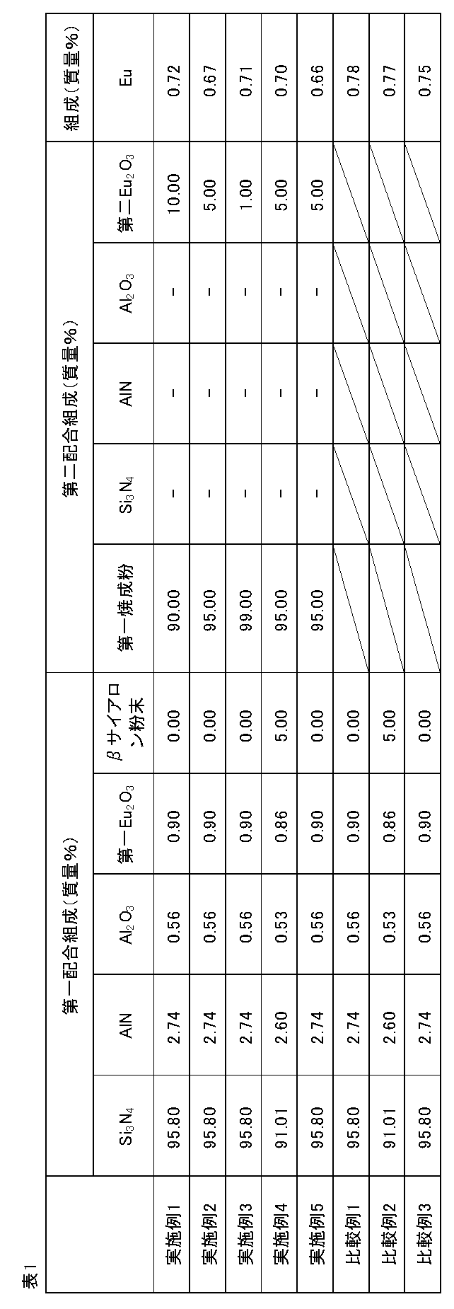

表2から、実施例1~5のβ型サイアロン蛍光体は、比較例1~3のβ型サイアロン蛍光体に比べて蛍光のピーク強度が高く、高輝度のβ型サイアロン蛍光体であることが分かった。
この出願は、2018年11月19日に出願された日本出願特願2018-216183号を基礎とする優先権を主張し、その開示の全てをここに取り込む。
Claims (8)
- ユウロピウムが固溶したβ型サイアロン蛍光体であって、
前記β型サイアロン蛍光体の個々の粒子における結晶方位を電子後方散乱回折像法により識別して結晶方位毎に区別した単結晶粒子を一次粒子と定義したとき、
前記一次粒子の断面積を画像解析により求めたときの、
前記β型サイアロン蛍光体の前記一次粒子の50%面積平均径をD50とし、
前記β型サイアロン蛍光体の前記一次粒子の10%面積平均径をD10としたとき、
D50が7.0μm以上20.0μm以下であり、
(D50-D10)/D50が0.60以下であるβ型サイアロン蛍光体。 - 請求項1に記載のβ型サイアロン蛍光体において、
前記β型サイアロン蛍光体の前記一次粒子の90%面積平均径をD90としたとき、
(D90-D10)/D50が1.45以下であるβ型サイアロン蛍光体。 - 請求項1または2に記載のβ型サイアロン蛍光体において、
一般式Si6-zAlzOzN8-z:Eu2+(0<Z≦4.2)で示されるβ型サイアロン蛍光体。 - 請求項1乃至3のいずれか一項に記載のβ型サイアロン蛍光体において、
前記β型サイアロン蛍光体のDV50粒径(JIS R1629:1997に準拠したレーザー回折散乱法による体積基準の積算分率における50%径)が5μm以上50μm以下であるβ型サイアロン蛍光体。 - 請求項1乃至4のいずれか一項に記載のβ型サイアロン蛍光体において、
複数の前記一次粒子同士が粒界を介して焼結した粒子を二次粒子と定義したとき、
前記β型サイアロン蛍光体の前記二次粒子数に対する前記一次粒子数の比が1.90以下であるβ型サイアロン蛍光体。 - 発光光源と波長変換部材とを含む発光装置であって、
前記波長変換部材は蛍光体を含み、
前記蛍光体が請求項1乃至5のいずれか一項に記載のβ型サイアロン蛍光体を含む発光装置。 - 請求項6に記載の発光装置において、
前記発光光源が、300nm~500nmの波長の光を発生するLEDチップを含む発光装置。 - 請求項6または7に記載の発光装置において、
前記蛍光体が、マンガンが固溶したKSF系蛍光体をさらに含む発光装置。
Priority Applications (4)
| Application Number | Priority Date | Filing Date | Title |
|---|---|---|---|
| DE112019005783.9T DE112019005783T5 (de) | 2018-11-19 | 2019-11-07 | β-Sialon-Leuchtstoff und lichtemittierende Vorrichtung |
| US17/294,721 US11702592B2 (en) | 2018-11-19 | 2019-11-07 | B-sialon phosphor and light emitting device |
| KR1020217015510A KR102706154B1 (ko) | 2018-11-19 | 2019-11-07 | β형 사이알론 형광체 및 발광 장치 |
| CN201980075937.6A CN113166644B (zh) | 2018-11-19 | 2019-11-07 | β型赛隆荧光体和发光装置 |
Applications Claiming Priority (2)
| Application Number | Priority Date | Filing Date | Title |
|---|---|---|---|
| JP2018-216183 | 2018-11-19 | ||
| JP2018216183 | 2018-11-19 |
Publications (1)
| Publication Number | Publication Date |
|---|---|
| WO2020105456A1 true WO2020105456A1 (ja) | 2020-05-28 |
Family
ID=70773632
Family Applications (1)
| Application Number | Title | Priority Date | Filing Date |
|---|---|---|---|
| PCT/JP2019/043689 Ceased WO2020105456A1 (ja) | 2018-11-19 | 2019-11-07 | β型サイアロン蛍光体および発光装置 |
Country Status (6)
| Country | Link |
|---|---|
| US (1) | US11702592B2 (ja) |
| KR (1) | KR102706154B1 (ja) |
| CN (1) | CN113166644B (ja) |
| DE (1) | DE112019005783T5 (ja) |
| TW (1) | TWI829803B (ja) |
| WO (1) | WO2020105456A1 (ja) |
Cited By (3)
| Publication number | Priority date | Publication date | Assignee | Title |
|---|---|---|---|---|
| JP2022148419A (ja) * | 2021-03-24 | 2022-10-06 | デンカ株式会社 | β型サイアロン蛍光体粉末および発光装置 |
| JP2023100542A (ja) * | 2022-01-06 | 2023-07-19 | 株式会社日立製作所 | シナリオ構築システム、シナリオ構築装置、および、シナリオ構築方法 |
| WO2024203353A1 (ja) * | 2023-03-30 | 2024-10-03 | デンカ株式会社 | 蛍光体粉末及び発光装置 |
Families Citing this family (1)
| Publication number | Priority date | Publication date | Assignee | Title |
|---|---|---|---|---|
| JP7282744B2 (ja) * | 2018-03-29 | 2023-05-29 | デンカ株式会社 | β型サイアロン蛍光体及び発光装置 |
Citations (4)
| Publication number | Priority date | Publication date | Assignee | Title |
|---|---|---|---|---|
| WO2012011444A1 (ja) * | 2010-07-20 | 2012-01-26 | 電気化学工業株式会社 | β型サイアロン、β型サイアロンの製造方法及び発光装置 |
| WO2012101899A1 (ja) * | 2011-01-26 | 2012-08-02 | 電気化学工業株式会社 | α型サイアロン、発光装置及びその用途 |
| WO2014115447A1 (ja) * | 2013-01-23 | 2014-07-31 | シャープ株式会社 | 発光装置 |
| WO2017122800A1 (ja) * | 2016-01-15 | 2017-07-20 | デンカ株式会社 | 蛍光体および発光装置 |
Family Cites Families (3)
| Publication number | Priority date | Publication date | Assignee | Title |
|---|---|---|---|---|
| KR101445624B1 (ko) * | 2009-11-10 | 2014-09-29 | 덴끼 가가꾸 고교 가부시키가이샤 | β형 사이알론, 그 제조 방법 및 그것을 사용한 발광 장치 |
| JPWO2014030637A1 (ja) * | 2012-08-22 | 2016-07-28 | デンカ株式会社 | βサイアロンの製造方法、βサイアロン及び発光装置 |
| JP6770353B2 (ja) * | 2016-07-01 | 2020-10-14 | デンカ株式会社 | β型サイアロン蛍光体、並びにそれを用いた発光部材及び発光装置 |
-
2019
- 2019-11-07 DE DE112019005783.9T patent/DE112019005783T5/de active Pending
- 2019-11-07 KR KR1020217015510A patent/KR102706154B1/ko active Active
- 2019-11-07 US US17/294,721 patent/US11702592B2/en active Active
- 2019-11-07 WO PCT/JP2019/043689 patent/WO2020105456A1/ja not_active Ceased
- 2019-11-07 CN CN201980075937.6A patent/CN113166644B/zh active Active
- 2019-11-13 TW TW108141091A patent/TWI829803B/zh active
Patent Citations (4)
| Publication number | Priority date | Publication date | Assignee | Title |
|---|---|---|---|---|
| WO2012011444A1 (ja) * | 2010-07-20 | 2012-01-26 | 電気化学工業株式会社 | β型サイアロン、β型サイアロンの製造方法及び発光装置 |
| WO2012101899A1 (ja) * | 2011-01-26 | 2012-08-02 | 電気化学工業株式会社 | α型サイアロン、発光装置及びその用途 |
| WO2014115447A1 (ja) * | 2013-01-23 | 2014-07-31 | シャープ株式会社 | 発光装置 |
| WO2017122800A1 (ja) * | 2016-01-15 | 2017-07-20 | デンカ株式会社 | 蛍光体および発光装置 |
Cited By (5)
| Publication number | Priority date | Publication date | Assignee | Title |
|---|---|---|---|---|
| JP2022148419A (ja) * | 2021-03-24 | 2022-10-06 | デンカ株式会社 | β型サイアロン蛍光体粉末および発光装置 |
| JP7676175B2 (ja) | 2021-03-24 | 2025-05-14 | デンカ株式会社 | β型サイアロン蛍光体粉末および発光装置 |
| JP2023100542A (ja) * | 2022-01-06 | 2023-07-19 | 株式会社日立製作所 | シナリオ構築システム、シナリオ構築装置、および、シナリオ構築方法 |
| JP7597748B2 (ja) | 2022-01-06 | 2024-12-10 | 株式会社日立製作所 | シナリオ構築システム、シナリオ構築装置、および、シナリオ構築方法 |
| WO2024203353A1 (ja) * | 2023-03-30 | 2024-10-03 | デンカ株式会社 | 蛍光体粉末及び発光装置 |
Also Published As
| Publication number | Publication date |
|---|---|
| US20220010205A1 (en) | 2022-01-13 |
| KR20210092216A (ko) | 2021-07-23 |
| TW202026402A (zh) | 2020-07-16 |
| TWI829803B (zh) | 2024-01-21 |
| DE112019005783T5 (de) | 2021-09-09 |
| US11702592B2 (en) | 2023-07-18 |
| CN113166644A (zh) | 2021-07-23 |
| CN113166644B (zh) | 2023-08-18 |
| KR102706154B1 (ko) | 2024-09-13 |
Similar Documents
| Publication | Publication Date | Title |
|---|---|---|
| JP7278924B2 (ja) | β型サイアロン蛍光体および発光装置 | |
| JP6572373B1 (ja) | β型サイアロン蛍光体の製造方法 | |
| TWI450946B (zh) | β型矽鋁氮氧化物、β型矽鋁氮氧化物之製造方法及發光裝置 | |
| JP5778699B2 (ja) | α型サイアロン、発光装置及びその用途 | |
| US11702592B2 (en) | B-sialon phosphor and light emitting device | |
| TWI458806B (zh) | β型矽鋁氮氧化物之製造方法、β型矽鋁氮氧化物及發光裝置 | |
| JP7588589B2 (ja) | β型サイアロン蛍光体および発光装置 | |
| JP7588075B2 (ja) | β型サイアロン蛍光体粒子および発光装置 | |
| KR102927320B1 (ko) | Eu 부활 β형 사이알론 형광체 입자, β형 사이알론 형광체 분말 및 발광 장치 | |
| JP2012025956A (ja) | β型サイアロンの製造方法 |
Legal Events
| Date | Code | Title | Description |
|---|---|---|---|
| 121 | Ep: the epo has been informed by wipo that ep was designated in this application |
Ref document number: 19886619 Country of ref document: EP Kind code of ref document: A1 |
|
| ENP | Entry into the national phase |
Ref document number: 20217015510 Country of ref document: KR Kind code of ref document: A |
|
| 122 | Ep: pct application non-entry in european phase |
Ref document number: 19886619 Country of ref document: EP Kind code of ref document: A1 |