WO2020105239A1 - 光学モジュールおよび距離測定装置 - Google Patents
光学モジュールおよび距離測定装置Info
- Publication number
- WO2020105239A1 WO2020105239A1 PCT/JP2019/032815 JP2019032815W WO2020105239A1 WO 2020105239 A1 WO2020105239 A1 WO 2020105239A1 JP 2019032815 W JP2019032815 W JP 2019032815W WO 2020105239 A1 WO2020105239 A1 WO 2020105239A1
- Authority
- WO
- WIPO (PCT)
- Prior art keywords
- light
- light beam
- optical
- optical module
- scanning
- Prior art date
- Legal status (The legal status is an assumption and is not a legal conclusion. Google has not performed a legal analysis and makes no representation as to the accuracy of the status listed.)
- Ceased
Links
Images




Classifications
-
- G—PHYSICS
- G02—OPTICS
- G02B—OPTICAL ELEMENTS, SYSTEMS OR APPARATUS
- G02B26/00—Optical devices or arrangements for the control of light using movable or deformable optical elements
- G02B26/08—Optical devices or arrangements for the control of light using movable or deformable optical elements for controlling the direction of light
- G02B26/10—Scanning systems
- G02B26/105—Scanning systems with one or more pivoting mirrors or galvano-mirrors
-
- G—PHYSICS
- G01—MEASURING; TESTING
- G01C—MEASURING DISTANCES, LEVELS OR BEARINGS; SURVEYING; NAVIGATION; GYROSCOPIC INSTRUMENTS; PHOTOGRAMMETRY OR VIDEOGRAMMETRY
- G01C3/00—Measuring distances in line of sight; Optical rangefinders
- G01C3/02—Details
- G01C3/06—Use of electric means to obtain final indication
-
- G—PHYSICS
- G01—MEASURING; TESTING
- G01S—RADIO DIRECTION-FINDING; RADIO NAVIGATION; DETERMINING DISTANCE OR VELOCITY BY USE OF RADIO WAVES; LOCATING OR PRESENCE-DETECTING BY USE OF THE REFLECTION OR RERADIATION OF RADIO WAVES; ANALOGOUS ARRANGEMENTS USING OTHER WAVES
- G01S17/00—Systems using the reflection or reradiation of electromagnetic waves other than radio waves, e.g. lidar systems
- G01S17/02—Systems using the reflection of electromagnetic waves other than radio waves
- G01S17/06—Systems determining position data of a target
- G01S17/08—Systems determining position data of a target for measuring distance only
- G01S17/10—Systems determining position data of a target for measuring distance only using transmission of interrupted, pulse-modulated waves
-
- G—PHYSICS
- G01—MEASURING; TESTING
- G01S—RADIO DIRECTION-FINDING; RADIO NAVIGATION; DETERMINING DISTANCE OR VELOCITY BY USE OF RADIO WAVES; LOCATING OR PRESENCE-DETECTING BY USE OF THE REFLECTION OR RERADIATION OF RADIO WAVES; ANALOGOUS ARRANGEMENTS USING OTHER WAVES
- G01S17/00—Systems using the reflection or reradiation of electromagnetic waves other than radio waves, e.g. lidar systems
- G01S17/02—Systems using the reflection of electromagnetic waves other than radio waves
- G01S17/06—Systems determining position data of a target
- G01S17/42—Simultaneous measurement of distance and other co-ordinates
-
- G—PHYSICS
- G01—MEASURING; TESTING
- G01S—RADIO DIRECTION-FINDING; RADIO NAVIGATION; DETERMINING DISTANCE OR VELOCITY BY USE OF RADIO WAVES; LOCATING OR PRESENCE-DETECTING BY USE OF THE REFLECTION OR RERADIATION OF RADIO WAVES; ANALOGOUS ARRANGEMENTS USING OTHER WAVES
- G01S7/00—Details of systems according to groups G01S13/00, G01S15/00, G01S17/00
- G01S7/48—Details of systems according to groups G01S13/00, G01S15/00, G01S17/00 of systems according to group G01S17/00
- G01S7/481—Constructional features, e.g. arrangements of optical elements
- G01S7/4814—Constructional features, e.g. arrangements of optical elements of transmitters alone
-
- G—PHYSICS
- G01—MEASURING; TESTING
- G01S—RADIO DIRECTION-FINDING; RADIO NAVIGATION; DETERMINING DISTANCE OR VELOCITY BY USE OF RADIO WAVES; LOCATING OR PRESENCE-DETECTING BY USE OF THE REFLECTION OR RERADIATION OF RADIO WAVES; ANALOGOUS ARRANGEMENTS USING OTHER WAVES
- G01S7/00—Details of systems according to groups G01S13/00, G01S15/00, G01S17/00
- G01S7/48—Details of systems according to groups G01S13/00, G01S15/00, G01S17/00 of systems according to group G01S17/00
- G01S7/481—Constructional features, e.g. arrangements of optical elements
- G01S7/4816—Constructional features, e.g. arrangements of optical elements of receivers alone
-
- G—PHYSICS
- G01—MEASURING; TESTING
- G01S—RADIO DIRECTION-FINDING; RADIO NAVIGATION; DETERMINING DISTANCE OR VELOCITY BY USE OF RADIO WAVES; LOCATING OR PRESENCE-DETECTING BY USE OF THE REFLECTION OR RERADIATION OF RADIO WAVES; ANALOGOUS ARRANGEMENTS USING OTHER WAVES
- G01S7/00—Details of systems according to groups G01S13/00, G01S15/00, G01S17/00
- G01S7/48—Details of systems according to groups G01S13/00, G01S15/00, G01S17/00 of systems according to group G01S17/00
- G01S7/481—Constructional features, e.g. arrangements of optical elements
- G01S7/4817—Constructional features, e.g. arrangements of optical elements relating to scanning
-
- G—PHYSICS
- G02—OPTICS
- G02B—OPTICAL ELEMENTS, SYSTEMS OR APPARATUS
- G02B26/00—Optical devices or arrangements for the control of light using movable or deformable optical elements
- G02B26/08—Optical devices or arrangements for the control of light using movable or deformable optical elements for controlling the direction of light
- G02B26/0816—Optical devices or arrangements for the control of light using movable or deformable optical elements for controlling the direction of light by means of one or more reflecting elements
- G02B26/0833—Optical devices or arrangements for the control of light using movable or deformable optical elements for controlling the direction of light by means of one or more reflecting elements the reflecting element being a micromechanical device, e.g. a MEMS mirror, DMD
-
- G—PHYSICS
- G02—OPTICS
- G02B—OPTICAL ELEMENTS, SYSTEMS OR APPARATUS
- G02B26/00—Optical devices or arrangements for the control of light using movable or deformable optical elements
- G02B26/08—Optical devices or arrangements for the control of light using movable or deformable optical elements for controlling the direction of light
- G02B26/10—Scanning systems
- G02B26/101—Scanning systems with both horizontal and vertical deflecting means, e.g. raster or XY scanners
-
- G—PHYSICS
- G02—OPTICS
- G02B—OPTICAL ELEMENTS, SYSTEMS OR APPARATUS
- G02B5/00—Optical elements other than lenses
- G02B5/18—Diffraction gratings
- G02B5/1866—Transmission gratings characterised by their structure, e.g. step profile, contours of substrate or grooves, pitch variations, materials
Definitions
- This technology relates to optical modules. More specifically, the present invention relates to an optical module that irradiates an object with a light beam, and a distance measuring device that uses the optical module.
- An optical module that irradiates a target with a light beam is used for applications such as distance measurement by measuring the spatial propagation time of light (ToF: Time of Flight) and object shape recognition.
- ToF Time of Flight
- an optical module there is known one that scans a light beam and detects reflected light from an object corresponding to each scanning position.
- an apparatus using slit light as scanning light has been proposed (see, for example, Patent Document 1).
- the light output of the light emitting unit can be reduced and the generation of noise due to external light can be suppressed compared to the case where the entire measurement target range is irradiated.
- a cylindrical lens is used to generate slit light (a linear light beam), and when the scanned light beam is incident, the incident angle deviates from the vertical incidence, and the line The phenomenon that the linear light beam distorts from a straight line to a curved line occurs.
- the light beam is distorted from a straight line, it becomes difficult to detect the reflected light from the object according to a certain scanning position with one row of the light receiving units arranged in a two-dimensional manner.
- the position of the reflected light shifts, the amount of light that can be detected decreases, and the distance accuracy deteriorates.
- the detection is performed in a plurality of columns, it is likely to be affected by noise due to external light.
- the width of the linear light beam is widened, it is necessary to increase the light output of the light emitting unit by that amount, resulting in an increase in power consumption.
- the light output cannot be increased due to safety regulations for the eyes.
- the present technology has been created in view of such a situation, and in an optical module that irradiates an object with a light beam and detects its reflected light, distortion of the optical beam is detected regardless of the incident angle of the scanned light beam.
- the purpose is to irradiate a non-linear light beam.
- a first side surface thereof is an optical scanning unit that scans a light beam in a predetermined scanning direction, and an optical surface that scans the light beam.
- the optical surface comprises a light conversion unit for converting into a linear light beam in a line direction substantially orthogonal to the scanning direction by the above, and a light detection unit for detecting reflected light from an object with respect to the linear light beam.
- An optical module and a distance measuring device in which the radius of curvature in the scanning direction is substantially equal to the distance from the virtual scanning center point in the scanning direction to the center point of the optical surface regardless of the position in the line direction. This brings about an effect of emitting a linear light beam without distortion.
- the light conversion unit may generate the linear light beam with the radius of curvature in the linear direction. This brings about an effect of generating a linear light beam orthogonal to the scanned light beam.
- the optical surface may satisfy the following conditional expression. This has the effect of causing a light beam to enter at an angle orthogonal to the optical surface in the direction perpendicular to the optical surface and emitting a linear light beam without distortion.
- z (y 2 / ry) / (1+ (1- (1 + ⁇ ) ⁇ y 2 / ry 2 ) 1/2 ) + A ⁇ y 4 + B ⁇ y 6 + C ⁇ y 8 + ...
- x, y, and z are coordinates on the X-axis, Y-axis, and Z-axis, respectively
- ⁇ is a conic constant
- A, B, and C are the fourth, sixth, and eighth non-dimensional coordinates, respectively. It is a spherical coefficient
- rx is the radius of curvature in the scanning direction
- ry is the radius of curvature in the line direction.
- the light conversion unit is either an optical lens, a diffraction grating having a sawtooth grating in the scanning direction, or a diffuser plate curved in the scanning direction. May be.
- the optical scanning unit may include a MEMS mirror. This brings about the effect of downsizing the optical module.
- the light detection unit includes a plurality of light receiving units, and detects reflected light from an object according to the scanning position of the linear light beam among the plurality of light receiving units. Only one of them may be selectively operated. As a result, the effect of suppressing the reception of unnecessary light and reducing the noise associated with unnecessary light is brought about.
- the first side face may further include a light emitting unit that emits light and a light emitting unit that emits light from the light emitting unit as the light beam having a predetermined angular width.
- the light emitting unit may be a laser light source.
- First embodiment (example in which an optical lens is used as a light conversion unit) 2.
- Second embodiment (example using a diffraction grating as a light conversion unit) 3.
- Third embodiment (example in which a diffusion plate is used as a light conversion unit)
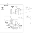
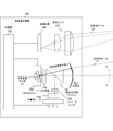
- FIG. 1 is a diagram illustrating a configuration example of a distance measuring device 100 according to the first embodiment of the present technology.
- the distance measuring device 100 is an example of an optical module that irradiates a target with a light beam and detects the reflected light, and is a device that measures the flight time of light and measures the distance to the target.
- the distance measuring device 100 includes a semiconductor laser 110, a collimator lens 120, a polarized light splitting prism 130, a quarter wavelength plate 140, a MEMS mirror 150, an optical lens 161, a condenser lens 170, and light detection.
- the device 180 and the control unit 190 are provided.
- the semiconductor laser 110 is a laser light source that emits a light beam. In order to make the line-shaped light beam thinner, it is desirable to use the edge-emitting semiconductor laser 110. Further, it is desirable that the light vertical confinement direction of the stripe-shaped light confinement portion provided in the semiconductor laser 110 is the line width direction (scanning direction). As the semiconductor laser 110, a surface emitting laser (VCSEL: Vertical Cavity Surface Emitting LASER) arranged in a line may be used.
- VCSEL Vertical Cavity Surface Emitting LASER
- the collimator lens 120 is a lens that converts a light beam emitted from the semiconductor laser 110 into a substantially parallel light beam.
- the light beam that has passed through the collimator lens 120 is incident on the polarized light splitting prism 130. Strictly speaking, the light beam that has passed through the collimator lens 120 corresponds to the range detected by one line-shaped light receiving unit irrespective of the distance while the beam having a predetermined angular width spreads according to the distance. It is desirable that the entire area of the target object is illuminated in a line.
- the collimator lens 120 is an example of the light irradiation unit described in the claims.
- the polarized light splitting prism 130 is a polarizing beam splitter (PBS: Polarizing Beam Splitter) that splits the incident light into a P (parallel: parallel) polarization component and an S (senkrecht: vertical) polarization component.
- PBS Polarizing Beam Splitter
- the polarized light splitting prism 130 mainly reflects the light beam of the S-polarized component and guides it to the MEMS mirror 150.
- the light beam is linearly polarized, and in the case of TE (Transverse Electric wave) mode light emission, it is polarized light whose polarization direction is orthogonal to the vertical optical confinement direction. Become. Therefore, almost all the light beams are reflected by the polarized light splitting prism 130.
- the horizontal light trapping direction which is orthogonal to the light vertical trapping direction, is generally a stripe with a wider width than the vertical direction. By utilizing this relationship, the line width can be adjusted by rotating the semiconductor laser 110 around the emission direction (optical axis).
- the light beam that has passed through the polarized light splitting prism 130 is detected by a photodetector that is separately provided, and the light intensity is measured to control the power supplied to the semiconductor laser 110 for emission. It is also possible to optimally control the intensity of the emitted light beam.
- polarized light splitting prism 130 polarized light splitting prism 130
- a parallel plate may be used, for example.
- the light splitting prism or the light splitting flat plate may not be used.
- the quarter-wave plate 140 is an optical functional element that gives a quarter-wave phase difference to the plane of polarization of incident light.
- the quarter-wave plate 140 converts the light beam reflected by the polarized light splitting prism 130 into a circularly polarized light beam and outputs the circularly polarized light beam to the MEMS mirror 150.
- the quarter-wave plate 140 converts the light beam reflected by the MEMS mirror 150 into a P-polarized linearly polarized beam and outputs it to the polarized light splitting prism 130. As a result, almost all the light beams pass through the polarized light splitting prism 130 and enter the optical lens 161.
- the MEMS (Micro Electro Mechanical Systems) mirror 150 is a micromachined electromechanical mirror.
- the MEMS mirror 150 reflects the circularly polarized beam incident from the quarter-wave plate 140.
- the MEMS mirror 150 scans the light beam in the vertical direction by rotationally oscillating. That is, the vertical direction is the scanning direction.
- the scanned light beam is incident on the quarter-wave plate 140 again, but as described above, almost all the light beam is transmitted through the polarized light splitting prism 130 and is incident on the optical lens 161.
- the MEMS mirror 150 is an example of the optical scanning unit described in the claims.
- the optical lens 161 is a lens that emits the light beam scanned by the MEMS mirror 150 as the emission light beam 11.
- the optical surface (S0) on the light incident side of the optical lens 161 is an optical plane.
- the optical surface (S1) on the light emission side has different radii of curvature (rx and ry) in the vertical (X) direction and the horizontal (Y) direction, respectively.
- the curvature in the horizontal (Y) direction is an optical surface shape for obtaining a desired horizontal line spread (HFOV: Horizontal Field of View). That is, the line direction in which the linear light beam is formed is the horizontal direction.
- This optical surface is not limited to a spherical surface, and may be a free-form surface shape or an aspherical surface shape.
- the surface shape of the optical surface (S1) may have a function of converting the incident Gaussian intensity distribution into a light beam having a top-flat intensity distribution in which the light intensity is uniformized. ..
- the radius of curvature rx in the vertical (X) direction is preferably set to be substantially equal to the length from the virtual scanning center point Ox shown in the figure to the emission side optical surface (S1) regardless of the position in the horizontal direction.
- the virtual scanning center point is a position of a point where the emitted light beams that are scanned when viewed from the irradiated object side are gathered when they are extended in the depth direction of the distance measuring device 100, and are also called virtual rotation center points. It Optically, it is a virtual light emitting point.
- the light beam 11 emitted by the optical lens 161 is irradiated on the object for distance measurement and is reflected and scattered.
- the reflected light from the object with respect to the outgoing light beam 11 is incident on the distance measuring device 100 as the reflected light beam 12.
- the optical lens 161 is an example of the light conversion unit described in the claims.
- the condenser lens 170 is a lens that condenses the reflected light beam 12 from the object.
- the reflected light beam 12 condensed by the condenser lens 170 is guided to the photodetector 180.
- the photodetector 180 detects the reflected light beam 12 from the object. As will be described later, the photodetector 180 is provided with a plurality of line-shaped light receiving portions on the surface for the condenser lens 170, and sequentially activates these to detect light.
- the photodetector 180 is an example of the photodetection unit described in the claims.
- the control unit 190 controls the distance measuring operation in the distance measuring device 100. That is, the control unit 190 performs the light emission timing of the semiconductor laser 110, the scanning position by the MEMS mirror 150, the synchronous control of the light receiving unit selection in the photo detector 180, and the measurement of the light detection timing. Thereby, the emitted light is reflected by the object and the flight time required until it is detected as reflected light is measured, and the distance to the object is measured. At that time, various methods such as a direct method of observing a reflected wave (direct ToF) and an indirect method by changing a phase shift of a rectangular wave (indirect ToF) can be used.
- the control unit 190 is an example of the measurement unit described in the claims.
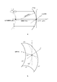
- FIG. 2 is a diagram showing an example of the surface shape of the optical surface (S1) of the optical lens 161 according to the first embodiment of the present technology.
- the optical surface (S1) is centered at a position separated from the virtual scanning center point Ox by the radius of curvature rx in the scanning direction along the Z axis orthogonal to the X axis indicating the scanning direction and the Y axis indicating the line direction. , And has a shape rotated by an axis parallel to the Y axis.
- the curves obtained from the cross section cut by the plane parallel to the YZ plane are always the same curves made with the radius of curvature ry0.
- a curve obtained from a cross section cut by a plane parallel to the XZ plane always has a radius of curvature rx0.
- the curve obtained from the cross section taken along the plane parallel to the YZ plane is an optical surface shape required to obtain a desired horizontal line spread (HFOV) as described above, and is not limited to a spherical surface. It may be a free-form surface shape or an aspherical shape.
- This optical surface shape can be expressed by the following conditional expression.
- z (y 2 / ry) / (1+ (1- (1 + ⁇ ) ⁇ y 2 / ry 2 ) 1/2 ) + A ⁇ y 4 + B ⁇ y 6 + C ⁇ y 8 + ... + (X 2 / rx) / (1+ (1-x 2 / rx 2 ) 1/2 )
- x, y, and z are coordinates on the X-axis, Y-axis, and Z-axis, respectively
- ⁇ is a conic constant
- A, B, and C are the fourth, sixth, and eighth non-dimensional coordinates, respectively.
- rx is the radius of curvature in the scanning direction
- ry is the radius of curvature in the line direction.
- the first term represented by the variable y and its higher-order terms are terms representing the lens surface shape in the y direction for generating a linear light beam
- the final term represented by the variable x is scanned.
- the term represents a lens shape in the x direction for forming a plane orthogonal to the light beam.
- FIG. 3 is a diagram showing a comparative example of the shape of the outgoing light beam 11 formed by the optical lens 161 according to the first embodiment of the present technology.
- scanning is performed because the optical surface shape of the optical lens 161 and the radius of curvature rx in the vertical (X) direction substantially match the length from the optical surface to the virtual scanning center point Ox.
- the light beam is always incident on the optical surface at an angle orthogonal to the vertical direction.
- the light beam is expanded (or narrowed) only by the radius of curvature ry in the Y direction, and the linear light beam emitted from the optical lens does not depend on the scanning position. In addition, it becomes a linear light beam without distortion.
- the toroidal surface has a radius of curvature ry in the Y direction, and is formed by a rotationally symmetric surface parallel to the Y axis and having a radius of curvature rx from the position on the Z axis of the optical surface as an axis. ..
- the optical surface (S0) on the light incident side of the optical lens is an optical plane, but the optical surface is not limited to this.
- the light-incident-side optical surface is formed in the same manner as the exit-side optical surface (S1) described above, and a straight light beam without distortion is generated by both the entrance-side and exit-side optical surfaces. Is also possible.
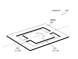
- FIG. 4 is a diagram showing an example of the structure of the MEMS mirror 150 according to the first embodiment of the present technology.
- the MEMS mirror 150 includes a mirror section 151, a holding section 152, and a hinge section 153.
- the mirror unit 151 is a mirror of several millimeters square that reflects the circularly polarized beam incident from the quarter-wave plate 140.
- the holding portion 152 is a member that is fixed to a fixing portion (not shown) of the MEMS mirror 150.
- the hinge part 153 is a member that supports the mirror part 151 and connects it to the holding part 152.
- the mirror section 151 is connected to the holding section 152 by two hinge sections 153, and rotationally vibrates by electromagnetic force or electrostatic capacitance about the broken line as an axis.
- the light beam reflected by the mirror unit 151 is scanned in the vertical direction by rotationally vibrating the mirror unit 151 in the vertical direction.
- FIG. 5 is a figure which shows the example of a structure of the photodetector 180 in 1st Embodiment of this technique.
- the photodetector 180 includes a plurality of light receiving units 181 divided vertically and horizontally.
- the light beam scanned at a certain position is reflected and scattered by the object, and is guided to the horizontally arranged line-shaped light receiving units 181. Since the linear light beam obtained here has no distortion and is linear, only the light receiving portions 182 of the lines necessary for detecting the reflected light are selectively turned on and the light receiving portions of other lines are turned on. It is easy to turn off 181. This makes it possible to reduce noise generated by the influence of unnecessary light from outside light such as sunlight.
- the reflected light beam 12 detected by the photodetector 180 has a vertical relationship opposite to that of the emitted light beam 11. Therefore, when the scanning by the MEMS mirror 150 is performed from top to bottom, it is necessary to control the photodetector 180 so that the light receiving portion 181 is activated from bottom to top.
- the linear light beam is formed by making the light beam orthogonal to the scanned light beam.
- a straight outgoing light beam 11 without distortion can be generated.
- FIG. 6 is a diagram illustrating a configuration example of the distance measuring device 100 according to the second embodiment of the present technology.
- the optical lens 161 was used to generate a linear light beam, but in the second embodiment, the diffraction grating 162 is used to generate a linear light beam. Therefore, except that the diffraction grating 162 is provided in place of the optical lens 161 in the first embodiment, it is the same as in the above-described first embodiment, and detailed description of other configurations is omitted.
- the diffraction grating 162 is an optical element having a sawtooth-shaped grating in the scanning direction. In the scanning direction, the Fresnel lens is formed, and its optical surface shape conforms to the surface shape of the above-described first embodiment. Glass or resin is assumed as the material of the diffraction grating 162.
- the diffraction grating 162 is an example of the light conversion unit described in the claims.
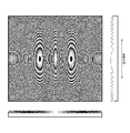
- FIG. 7 is a figure which shows the 1st example of the diffraction grating 162 in 2nd Embodiment of this technique.
- a first example of the diffraction grating 162 is a Fresnel lens having stepped gratings in both the scanning direction and the direction orthogonal to the scanning direction. That is, it is equivalent to the optical surface of the above-described first embodiment realized by the Fresnel lens.
- a sawtooth shape may be formed literally by cutting, or a step shape may be formed by a semiconductor lithography process.
- a stepped shape 8 levels
- a linear light beam having a desired divergence angle is generated.
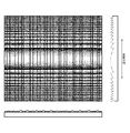
- FIG. 8 is a diagram showing a second example of the diffraction grating 162 according to the second embodiment of the present technology.
- a second example of the diffraction grating 162 is a Fresnel lens having a sawtooth grating in the scanning direction and a rectangular grating in the direction orthogonal to the scanning direction.
- the ⁇ first-order light is used to generate a linear light beam having a desired divergence angle.
- FIG. 9 is a diagram showing a third example of the diffraction grating 162 according to the second embodiment of the present technology.
- a third example of the diffraction grating 162 is a Fresnel lens provided with a sawtooth grating in the scanning direction, a linear diffusion plate is provided in the direction orthogonal to the scanning direction, and a desired spread angle is provided only in the horizontal direction. To generate a linear light beam.
- the shapes in the first to third examples can be processed on a curved surface, they can be applied to the lens surface shape, but the ease of processing and batch production by processing at the wafer level can be applied. Considering this, processing into an optical plane is more preferable.
- the linear light beam is formed by making it orthogonal to the scanned light beam to form a straight line without distortion.
- a shaped outgoing light beam 11 can be generated.
- FIG. 10 is a diagram illustrating a configuration example of the distance measuring device 100 according to the third embodiment of the present technology.
- the optical lens 161 was used to generate a linear light beam, but in the third embodiment, the diffusion plate 163 is used to generate a linear light beam. Therefore, except that the diffusion plate 163 is provided instead of the optical lens 161 in the first embodiment, it is the same as the above-described first embodiment, and detailed description of other configurations will be omitted.
- the diffuser plate 163 is a curved diffuser plate having a radius of curvature rx when viewed from the virtual scanning center point.
- the curvature radius rx of the curved diffusion plate 163 in the vertical (X) direction is preferably set to be substantially equal to the length from the virtual scanning center point to the emission side optical surface regardless of the horizontal position.
- the scanned light beam is always incident at an angle perpendicular to the optical surface in the direction perpendicular to the optical surface, and the linear portion of the diffusion plate 163 allows light to be emitted only in the direction perpendicular to the scanning direction.
- the beam is expanded. Therefore, the linear light beam emitted from the diffusion plate 163 becomes a linear light beam without distortion regardless of the scanning position.
- the virtual scanning center point coincides with the rotation center position of the MEMS mirror 150.
- the diffuser plate 163 is an example of the light conversion unit described in the claims.
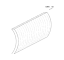
- FIG. 11 is a diagram showing an example of the shape of the diffusion plate 163 according to the third embodiment of the present technology.
- the diffusion plate 163 is curved in the vertical direction, while the direction orthogonal to the vertical direction has a linear shape. Therefore, unlike the surface shape of the XY toroidal surface such as a cylindrical lens, it is possible to generate a linear light beam without distortion.
- a linear light beam is formed so as to be orthogonal to the scanned light beam, and thus a straight line without distortion can be obtained.
- a shaped outgoing light beam 11 can be generated.
- the intensity of light detected at is kept high. Further, it is possible to achieve detection efficiency that does not depend on the position of the light receiving unit 181. Since the detection efficiency of light in the light receiving unit 181 is improved, the light output of the semiconductor laser 110, which is the light emitting unit, can be suppressed. This leads to improvement in reliability of the semiconductor laser 110 and reduction in power consumption of the distance measuring device 100. It also leads to improved eye safety.
- the distance measuring apparatus 100 can be downsized and the cost can be reduced. Further, the trouble of optical adjustment caused by the addition of the distortion correction optical element and the problem of displacement due to the environment do not occur.
- the present technology may have the following configurations.
- An optical scanning unit that scans a light beam in a predetermined scanning direction
- a light conversion unit that converts the scanned light beam into a linear light beam in a line direction substantially orthogonal to the scanning direction by an optical surface
- a light detection unit for detecting the reflected light from the object with respect to the linear light beam
- the optical module is an optical module in which a radius of curvature in the scanning direction is substantially equal to a distance from a virtual scanning center point in the scanning direction to a center point of the optical surface regardless of a position in the linear direction.
- the optical module according to (2) above which has a shape rotated about an axis parallel to the Y-axis about a position separated by a radius.
- x, y, and z are coordinates on the X-axis, Y-axis, and Z-axis, respectively
- ⁇ is a conic constant
- A, B, and C are the fourth, sixth, and eighth non-dimensional coordinates, respectively. It is a spherical coefficient
- rx is a radius of curvature in the scanning direction
- ry is a radius of curvature in the line direction.
- MEMS Micro Electro Mechanical Systems
- a light emitting part that emits light The optical module according to any one of (1) to (9), further comprising: a light irradiation unit that irradiates light from the light emitting unit as the light beam having a predetermined angular width.
- a light irradiation unit that irradiates light from the light emitting unit as the light beam having a predetermined angular width.
- the light emitting unit is a laser light source.
- a light emitting part that emits light
- a light irradiation unit that irradiates the light from the light emitting unit as a light beam having a predetermined angular width
- An optical scanning unit for scanning the light beam in a predetermined direction
- a light conversion unit for converting the scanned light beam into a linear light beam in a line direction substantially orthogonal to the scanning direction
- a light detection unit for detecting the reflected light from the object to the linear light beam
- the light irradiation unit comprises a measuring unit for measuring a distance from the object by measuring a flight time, which is a time from the light irradiation to the light detection unit detecting the reflected light
- the light conversion unit is a distance measuring device having an optical surface in which a radius of curvature in the scanning direction is substantially equal to a distance from a virtual scanning center point in the scanning direction to a center point of the optical surface regardless of the position in the line direction.
- Emitted light beam 12 Reflected light beam 100
- Distance measuring device 110
- Semiconductor laser 120
- Collimator lens 130
- Polarized light splitting prism 140
- 1 ⁇ 4 wavelength plate 150
- MEMS mirror 151
- Mirror part 152
- Holding part 153
- Hinge part 161
- Optical lens 162 Diffraction grating 163
- Condensing lens 180
- Photodetector 181
Landscapes
- Physics & Mathematics (AREA)
- Engineering & Computer Science (AREA)
- General Physics & Mathematics (AREA)
- Radar, Positioning & Navigation (AREA)
- Remote Sensing (AREA)
- Computer Networks & Wireless Communication (AREA)
- Electromagnetism (AREA)
- Optics & Photonics (AREA)
- Optical Radar Systems And Details Thereof (AREA)
- Measurement Of Optical Distance (AREA)
- Mechanical Optical Scanning Systems (AREA)
- Mechanical Light Control Or Optical Switches (AREA)
Abstract
本発明は、光ビームを対象物に照射してその反射光を検出する光学モジュールにおいて、走査した光ビームの入射角度によらずに、歪のない線状の光ビームを照射することを目的とする。 本発明の光学モジュールにおいて、光走査部(150)は、光ビームを所定方向(垂直方向)に走査する。光変換部(161)は、走査された光ビームを走査方向と略直交する線方向(水平方向)の線状光ビームに変換する。光検出部(180)は、線状光ビームに対する対象物からの反射光を検出する。光変換部(161)は、走査方向の曲率半径(rx)が前記線方向の位置によらず走査方向の仮想走査中心点(Ox)から光学面(S1)の中心点(A)までの距離と略等しい光学面(S1)を有する。 本発明の光学モジュールは、距離測定装置に適用できる。
Description
本技術は、光学モジュールに関する。詳しくは、光ビームを対象物に照射する光学モジュール、および、その光学モジュールを利用した距離測定装置に関する。
光ビームを対象物に照射する光学モジュールは、光の空間伝搬時間計測(ToF:Time of Flight)による距離の測定や、物体の形状認識などの用途に利用される。そのような光学モジュールとして、光ビームを走査して、それぞれの走査位置に対応する物体からの反射光を検出するものが知られている。例えば、走査光としてスリット光を用いた装置が提案されている(例えば、特許文献1参照。)。
上述の従来技術では、測定対象範囲全面に照射する場合と比べて、発光部の光出力を低減でき、外光によるノイズの発生を抑制することができる。しかしながら、この従来技術では、スリット光(線状の光ビーム)を生成するためにシリンドリカルレンズが用いられており、走査した光ビームを入射した際に、その入射角度が垂直入射からずれるに従って、線状の光ビームは直線から曲線に歪むという現象が生じる。光ビームが直線から歪んだ場合、2次元状に配列された受光部の1つの列で、ある走査位置に応じた物体からの反射光を検出することは難しくなる。具体的には、1列の受光部の端の方では、反射光の位置がずれ、検出できる光量が減少してしまい、距離精度の低下が生じる。これに対し、複数の列で検出するようにした場合、外光によるノイズの影響を受けやすくなる。また、線状の光ビームの幅を広げた場合、その分、発光部の光出力を上げる必要があり、消費電力が増加してしまう。しかも、目への安全規定により光出力を上げることができない場合もある。
本技術はこのような状況に鑑みて生み出されたものであり、光ビームを対象物に照射してその反射光を検出する光学モジュールにおいて、走査した光ビームの入射角度によらずに、歪のない線状の光ビームを照射することを目的とする。
本技術は、上述の問題点を解消するためになされたものであり、その第1の側面は、光ビームを所定の走査方向に走査する光走査部と、上記走査された光ビームを光学面によって上記走査方向と略直交する線方向の線状光ビームに変換する光変換部と、上記線状光ビームに対する対象物からの反射光を検出する光検出部とを具備し、上記光学面は、上記走査方向の曲率半径が上記線方向の位置によらず上記走査方向の仮想走査中心点から上記光学面の中心点までの距離と略等しい光学モジュールおよび距離測定装置である。これにより、歪みのない線状の光ビームを出射させるという作用をもたらす。
また、この第1の側面において、上記光変換部は、上記線方向の曲率半径により上記線状光ビームを生成するようにしてもよい。これにより、走査された光ビームと直交する線状光ビームを生成するという作用をもたらす。
また、この第1の側面において、上記光学面は、上記走査方向を示すX軸および上記線方向を示すY軸に直交するZ軸に沿って上記光学面におけるX=0の面上のZ位置から上記走査方向の曲率半径だけ離れた位置を中心としてY軸に平行な軸で回転させた形状を備えてもよい。これにより、光学面に対して垂直方向に直交した角度で光ビームを入射させるという作用をもたらす。
また、この第1の側面において、上記光学面は、以下の条件式を満足するようにしてもよい。光学面に対して垂直方向に直交した角度で光ビームを入射させて、歪みのない線状の光ビームを出射させるという作用をもたらす。
z=(y2/ry)/(1+(1-(1+κ)・y2/ry2)1/2)
+A・y4+B・y6+C・y8+…
+(x2/rx)/(1+(1-x2/rx2)1/2)
ただし、x、y、zはそれぞれX軸、Y軸、Z軸上の座標であり、κはコーニック定数であり、A、B、Cはそれぞれ第4次、第6次、第8次の非球面係数であり、rxは上記走査方向の曲率半径であり、ryは上記線方向の曲率半径である。
z=(y2/ry)/(1+(1-(1+κ)・y2/ry2)1/2)
+A・y4+B・y6+C・y8+…
+(x2/rx)/(1+(1-x2/rx2)1/2)
ただし、x、y、zはそれぞれX軸、Y軸、Z軸上の座標であり、κはコーニック定数であり、A、B、Cはそれぞれ第4次、第6次、第8次の非球面係数であり、rxは上記走査方向の曲率半径であり、ryは上記線方向の曲率半径である。
また、この第1の側面において、上記光変換部は、光学レンズ、上記走査方向に対して鋸歯形状の格子を有する回折格子、または、上記走査方向に対して湾曲した拡散板の何れかであってもよい。
また、この第1の側面において、上記光走査部は、MEMSミラーを備えてもよい。これにより、光学モジュールを小型化するという作用をもたらす。
また、この第1の側面において、上記光検出部は、複数の受光部を備え、上記複数の受光部のうち、上記線状光ビームの走査位置に応じた物体からの反射光を検出するもののみを選択的に動作させるようにしてもよい。これにより、不要光の受光を抑止して、不要光に伴うノイズを低減させるという作用をもたらす。
また、この第1の側面において、光を発する発光部と、上記発光部からの光を所定の角度幅の上記光ビームとして照射する光照射部とをさらに具備してもよい。この場合において、上記発光部は、レーザ光源であってもよい。
以下、本技術を実施するための形態(以下、実施の形態と称する)について説明する。説明は以下の順序により行う。
1.第1の実施の形態(光変換部として光学レンズを用いた例)
2.第2の実施の形態(光変換部として回折格子を用いた例)
3.第3の実施の形態(光変換部として拡散板を用いた例)
1.第1の実施の形態(光変換部として光学レンズを用いた例)
2.第2の実施の形態(光変換部として回折格子を用いた例)
3.第3の実施の形態(光変換部として拡散板を用いた例)
<1.第1の実施の形態>
[距離測定装置]
図1は、本技術の第1の実施の形態における距離測定装置100の構成例を示す図である。
[距離測定装置]
図1は、本技術の第1の実施の形態における距離測定装置100の構成例を示す図である。
距離測定装置100は、光ビームを対象物に照射してその反射光を検出する光学モジュールの一例であり、光の飛行時間を計測して対象物との距離を測定する装置である。この距離測定装置100は、半導体レーザ110と、コリメータレンズ120と、偏光光分割プリズム130と、1/4波長板140と、MEMSミラー150と、光学レンズ161と、集光レンズ170と、光検出器180と、制御部190とを備える。
半導体レーザ110は、光ビームを出射するレーザ光源である。ライン状の光ビームをより細いラインにするためには、端面発光型の半導体レーザ110を用いることが望ましい。また、半導体レーザ110に設けられたストライプ状の光閉じ込め部の光縦閉じ込め方向がラインの幅方向(走査方向)となっていることが望ましい。なお、この半導体レーザ110として、ライン状に配列された面発光レーザ(VCSEL:Vertical Cavity Surface Emitting LASER)を利用してもよい。なお、半導体レーザ110は、特許請求の範囲に記載の発光部の一例である。
コリメータレンズ120は、半導体レーザ110から出射された光ビームを、略平行な光ビームにするレンズである。このコリメータレンズ120を通過した光ビームは、偏光光分割プリズム130に入射される。厳密には、このコリメータレンズ120を通過した光ビームは、距離に応じて所定の角度幅のビームが広がる一方で、距離によらずにある1つのライン状の受光部が検出する範囲に相当する被対象物体のライン状の範囲全体に照射される状況となっていることが望ましい。なお、コリメータレンズ120は、特許請求の範囲に記載の光照射部の一例である。
偏光光分割プリズム130は、入射光をP(parallel:平行)偏光成分とS(senkrecht:垂直)偏光成分とに分割する偏光ビームスプリッタ(PBS:Polarizing Beam Splitter)である。この偏光光分割プリズム130は、S偏向成分の光ビームを主に反射して、MEMSミラー150に導く。
半導体レーザ110として端面発光型の半導体レーザを利用した場合、光ビームは直線偏光となっており、TE(Transverse Electric wave)モード発光の場合には偏光方向が光縦閉じ込め方向と直交する偏光光となる。そのため、偏光光分割プリズム130でほぼ全ての光ビームは反射することになる。光縦閉じ込め方向と直交する光横閉じ込め方向は、縦方向に比べて広い幅ストライプとなっていることが一般的である。この関係を利用して、出射方向(光軸)を軸として半導体レーザ110を回転させることにより、ライン幅を調整することも可能である。
また、図示しないが、偏光光分割プリズム130を透過した光ビームを、別途設けた光検出器により検出し、その光強度を測定することで、半導体レーザ110に供給する電力を制御して、出射される光ビームの強度を最適に制御することも可能である。
なお、偏光光分割の実現例として、プリズム(偏光光分割プリズム130)を用いた例を示したが、例えば平行平板を利用するようにしてもよい。また、MEMSミラー150への入射方向とMEMSミラー150からの出射方向とを異なる方向にすることにより、光分割プリズムや光分割平板を用いずに構成してもよい。
1/4波長板140は、入射された光の偏光面に1/4波長の位相差を与える光学機能素子である。この例では、1/4波長板140は、偏光光分割プリズム130によって反射された光ビームを円偏光ビームに変えてMEMSミラー150に出射する。また、1/4波長板140は、MEMSミラー150によって反射された光ビームをP偏光の直線偏光ビームに変えて偏光光分割プリズム130に出射する。これにより、ほぼすべての光ビームは偏光光分割プリズム130を透過し、光学レンズ161に入射される。
MEMS(Micro Electro Mechanical Systems)ミラー150は、微細加工された電気機械式のミラーである。このMEMSミラー150は、1/4波長板140から入射された円偏光ビームを反射する。その際、MEMSミラー150は、回転振動することにより、光ビームを垂直方向に走査する。すなわち、垂直方向が走査方向となる。走査された光ビームは、再び1/4波長板140に入射されるが、上述の通り、ほぼすべての光ビームは偏光光分割プリズム130を透過し、光学レンズ161に入射される。なお、MEMSミラー150は、特許請求の範囲に記載の光走査部の一例である。
光学レンズ161は、MEMSミラー150によって走査された光ビームを、出射光ビーム11として出射するレンズである。この光学レンズ161は、光入射側の光学面(S0)は、光学平面となっている。光出射側の光学面(S1)は、垂直(X)方向、および、水平(Y)方向にそれぞれ異なる曲率半径(rxおよびry)を有する。水平(Y)方向の曲率は、所望の水平方向ライン広がり(HFOV:Horizontal Field of View)を得るための光学面形状となっている。すなわち、線状光ビームが形成される線方向は、水平方向になる。この光学面は、球面に限定されず、自由曲面形状や非球面形状であってもよい。また、この光学面(S1)の面形状が、入射されたガウス形状の強度分布を、光強度が均一化されたトップフラット形状の強度分布をもつ光ビームに変換する機能を有してもよい。
垂直(X)方向の曲率半径rxは、水平方向の位置によらず、同図に示す仮想走査中心点Oxから出射側光学面(S1)までの長さと略等しく設定されていることが望ましい。なお、仮想走査中心点とは、被照射物体側からみた走査された出射光ビームを、それぞれ距離測定装置100の奥行方向に延長したときに集まる点の位置であり、仮想回転中心点とも呼称される。また、光学的には、仮想発光点である。
光学レンズ161による出射光ビーム11は、測距の対象物に照射され、反射散乱される。出射光ビーム11に対する対象物からの反射光は、反射光ビーム12として距離測定装置100に入射される。なお、光学レンズ161は、特許請求の範囲に記載の光変換部の一例である。
集光レンズ170は、対象物からの反射光ビーム12を集光するレンズである。この集光レンズ170により集光された反射光ビーム12は、光検出器180に導かれる。
光検出器180は、対象物からの反射光ビーム12を検出するものである。この光検出器180は、後述するように、集光レンズ170に対する面に複数のライン状の受光部を備えており、これらを順次有効にすることにより光を検出する。なお、光検出器180は、特許請求の範囲に記載の光検出部の一例である。
制御部190は、距離測定装置100における測距動作を制御するものである。すなわち、この制御部190は、半導体レーザ110の発光タイミング、MEMSミラー150による走査位置、光検出器180における受光部選択の同期制御、光検出タイミングの計測を行う。これにより、発光した光が被対象物で反射されて、反射光として検出されるまでに要した飛行時間が計測され、被対象物体までの距離が測定される。その際、反射波を観測する直接的な手法(ダイレクトToF)や、矩形波の移相の変化による間接的な手法(インダイレクトToF)などの様々な手法を用いることができる。なお、制御部190は、特許請求の範囲に記載の測定部の一例である。
なお、この例では、水平方向に広がったライン状の光ビームをMEMSミラー150によって垂直方向に走査する例を示した。ただし、垂直方向に広がったライン状の光ビームをMEMSミラー150によって水平方向に走査するようにしてもよい。
[光学レンズ]
図2は、本技術の第1の実施の形態における光学レンズ161の光学面(S1)の面形状の例を示す図である。
図2は、本技術の第1の実施の形態における光学レンズ161の光学面(S1)の面形状の例を示す図である。
同図におけるaに示すように、X=0のYZ平面において、Z軸上を中心とする任意の曲率半径ryで描かれる曲線がある。この曲線上の任意の点からZ軸に平行にrx離れた位置を中心に、XZ平面と平行に(すなわち、Y軸に平行な軸を中心に)回転することによって、曲面が描かれる。このようにして描かれた曲面が、同図におけるbに示す光学面(S1)となる。すなわち、光学面(S1)は、走査方向を示すX軸および線方向を示すY軸に直交するZ軸に沿って、仮想走査中心点Oxから走査方向の曲率半径rxだけ離れた位置を中心として、Y軸に平行な軸で回転させた形状を有する。
同図におけるbに示すように、YZ平面に平行な面で切り取った断面から得られる曲線は、常に曲率半径ry0で作られる同一の曲線となる。また、XZ平面に平行な面で切り取った断面から得られる曲線は、常に曲率半径rx0となる。なお、YZ平面に平行な面で切り取った断面から得られる曲線は、上述のように、所望の水平方向ライン広がり(HFOV)を得るために必要な光学面形状であり、球面に限定されず、自由曲面形状や非球面形状であってもよい。
この光学面形状は、以下の条件式で表すことができる。
z=(y2/ry)/(1+(1-(1+κ)・y2/ry2)1/2)
+A・y4+B・y6+C・y8+…
+(x2/rx)/(1+(1-x2/rx2)1/2)
ただし、x、y、zはそれぞれX軸、Y軸、Z軸上の座標であり、κはコーニック定数であり、A、B、Cはそれぞれ第4次、第6次、第8次の非球面係数であり、rxは走査方向の曲率半径であり、ryは線方向の曲率半径である。変数yで表される第1項およびその高次項までが、ライン状の光ビームを生成するためのy方向のレンズ面形状を表す項であり、変数xで表される最終項が、走査された光ビームと直交する面を作るためのx方向のレンズ形状を表す項となる。
z=(y2/ry)/(1+(1-(1+κ)・y2/ry2)1/2)
+A・y4+B・y6+C・y8+…
+(x2/rx)/(1+(1-x2/rx2)1/2)
ただし、x、y、zはそれぞれX軸、Y軸、Z軸上の座標であり、κはコーニック定数であり、A、B、Cはそれぞれ第4次、第6次、第8次の非球面係数であり、rxは走査方向の曲率半径であり、ryは線方向の曲率半径である。変数yで表される第1項およびその高次項までが、ライン状の光ビームを生成するためのy方向のレンズ面形状を表す項であり、変数xで表される最終項が、走査された光ビームと直交する面を作るためのx方向のレンズ形状を表す項となる。
図3は、本技術の第1の実施の形態における光学レンズ161により形成される出射光ビーム11の形状の比較例を示す図である。
ここまで説明したように、光学レンズ161の光学面形状、および、垂直(X)方向の曲率半径rxが光学面から仮想走査中心点Oxまでの長さと略一致していることにより、走査された光ビームは、常に光学面に対して垂直方向に直交した角度で入射されることとなる。これにより、同図におけるaに示すように、Y方向の曲率半径ryによってのみ光ビームが広げられ(または、狭められ)、光学レンズを出射したライン状の光ビームは、その走査位置によらずに、歪むことなく直線状の光ビームとなる。
一方、同図におけるbに示すように、例えばシリンドリカルレンズなどのXYトロイダル面の面形状を用いた場合には、上述の実施の形態とは異なり、歪みのない直線状の光ビームを得ることは困難である。このトロイダル面は、Y方向の曲率半径ryを有し、Y軸と平行な、光学面のZ軸上の位置から曲率半径rxの位置を軸とする回転対称な面で形成されたものである。
なお、上述の実施の形態では、光学レンズの光入射側の光学面(S0)を光学平面としたが、これに限定されるものではない。例えば、この光入射側の光学面も上述の出射側の光学面(S1)と同様に形成して、入射側および出射側両方の光学面によって、歪みのない直線状の光ビームを生成することも可能である。
[MEMSミラー]
図4は、本技術の第1の実施の形態におけるMEMSミラー150の構造の例を示す図である。
図4は、本技術の第1の実施の形態におけるMEMSミラー150の構造の例を示す図である。
MEMSミラー150は、ミラー部151と、保持部152と、ヒンジ部153とを備える。ミラー部151は、1/4波長板140から入射された円偏光ビームを反射する数ミリ角のミラーである。保持部152は、MEMSミラー150の(図示しない)固定部に固定する部材である。ヒンジ部153は、ミラー部151を支持して保持部152につなげる部材である。
ミラー部151は、2か所のヒンジ部153によって保持部152とつながっており、図示された破線を軸として、電磁力または静電容量によって回転振動する。図1の例では、ミラー部151が垂直方向に回転振動することにより、ミラー部151において反射された光ビームが垂直方向に走査される。
[光検出器]
図5は、本技術の第1の実施の形態における光検出器180の構造の例を示す図である。
図5は、本技術の第1の実施の形態における光検出器180の構造の例を示す図である。
光検出器180は、垂直方向および水平方向に分割された複数の受光部181を備える。ある位置に走査された光ビームは、被対象物で反射散乱され、水平に並んだライン状の受光部181に導かれる。ここで得られるライン状の光ビームは、歪みがなく直線状であるため、その反射光の検出のために必要なラインの受光部182のみを選択的にオンにして、他のラインの受光部181をオフにすることが容易である。これによって、太陽光などの外光からの不要光の影響により発生するノイズを低減することが可能となる。
なお、この光検出器180において検出される反射光ビーム12は、出射光ビーム11とは上下関係が逆になる。したがって、MEMSミラー150による走査が上から下に行われた場合には、光検出器180においては下から上に受光部181を有効にしていくよう制御する必要がある。
このように、本技術の第1の実施の形態によれば、光学レンズ161の光学面形状を利用して、走査された光ビームと直交させて、ライン状の光ビームを形成することにより、歪みのない直線状の出射光ビーム11を生成することができる。
<2.第2の実施の形態>
[距離測定装置]
図6は、本技術の第2の実施の形態における距離測定装置100の構成例を示す図である。
[距離測定装置]
図6は、本技術の第2の実施の形態における距離測定装置100の構成例を示す図である。
上述の第1の実施の形態では光学レンズ161を用いてライン状の光ビームを生成していたが、この第2の実施の形態では回折格子162を用いてライン状の光ビームを生成する。したがって、第1の実施の形態における光学レンズ161に代えて回折格子162を備える点以外は上述の第1の実施の形態と同様であるため、他の構成については詳細な説明を省略する。
回折格子162は、走査方向に対して鋸歯形状の格子を有する光学素子である。走査方向については、フレネルレンズが形成されている状態であり、その光学面形状は上述の第1の実施の形態の面形状に準ずるものとなる。この回折格子162の素材としては、ガラスまたは樹脂が想定される。なお、回折格子162は、特許請求の範囲に記載の光変換部の一例である。
また、走査方向に直交する方向の面形状は、光学平面に対して加工が可能である様々な形状を適用することができる。以下に、その具体例を示す。
[回折格子]
図7は、本技術の第2の実施の形態における回折格子162の第1の例を示す図である。
図7は、本技術の第2の実施の形態における回折格子162の第1の例を示す図である。
この回折格子162の第1の例は、走査方向および走査方向に直交する方向の両者に、階段状(ステップ状)の格子を備えるフレネルレンズである。すなわち、上述の第1の実施の形態の光学面をフレネルレンズにより実現したものと等価である。鋸歯形状の作製においては、切削加工により、文字通り鋸歯の形状にしたものでもよく、また、半導体リソグラフィプロセスにより、階段状(ステップ状)の形状にしたものでもよい。同図では、鋸歯形状の一例として、階段状(8レベル)の形状の例を示している。これにより、所望の広がり角のライン状の光ビームを生成する。
図8は、本技術の第2の実施の形態における回折格子162の第2の例を示す図である。
この回折格子162の第2の例は、走査方向に鋸歯形状の格子を備えるとともに、走査方向に直交する方向に矩形形状の格子を備えるフレネルレンズである。これにより、±1次光を利用して、所望の広がり角のライン状の光ビームを生成する。
図9は、本技術の第2の実施の形態における回折格子162の第3の例を示す図である。
この回折格子162の第3の例は、走査方向に鋸歯形状の格子を備えるフレネルレンズであるとともに、走査方向に直交する方向には線状の拡散板を設け、水平方向のみに所望の広がり角のライン状の光ビームを生成する。
なお、これら第1乃至第3の例における形状が曲面に対して加工可能である場合、レンズ面形状に適用することも可能であるが、加工の容易性やウエハレベルでの加工によるバッチ生産を考慮すると、光学平面への加工の方がより望ましい。
このように、本技術の第2の実施の形態によれば、回折格子162を利用して、走査された光ビームと直交させて、ライン状の光ビームを形成することにより、歪みのない直線状の出射光ビーム11を生成することができる。
<3.第3の実施の形態>
[距離測定装置]
図10は、本技術の第3の実施の形態における距離測定装置100の構成例を示す図である。
[距離測定装置]
図10は、本技術の第3の実施の形態における距離測定装置100の構成例を示す図である。
上述の第1の実施の形態では光学レンズ161を用いてライン状の光ビームを生成していたが、この第3の実施の形態では拡散板163を用いてライン状の光ビームを生成する。したがって、第1の実施の形態における光学レンズ161に代えて拡散板163を備える点以外は上述の第1の実施の形態と同様であるため、他の構成については詳細な説明を省略する。
拡散板163は、仮想走査中心点から見て曲率半径rxとなるように湾曲した拡散板である。この湾曲した拡散板163の垂直(X)方向の曲率半径rxは、水平方向の位置によらず仮想走査中心点から出射側光学面までの長さと略等しく設定されていることが望ましい。これにより、走査された光ビームは、常に光学面に対して垂直方向に直交した角度で入射されることになり、拡散板163の線状の部分によって走査方向に対して垂直な方向のみに光ビームが広げられる。したがって、拡散板163を出射したライン状の光ビームは、その走査位置によらずに、歪むことなく直線状の光ビームとなる。この例においては、仮想走査中心点は、MEMSミラー150の回転中心位置と一致している。なお、拡散板163は、特許請求の範囲に記載の光変換部の一例である。
図11は、本技術の第3の実施の形態における拡散板163の形状の例を示す図である。
この例では、拡散板163は、垂直方向に湾曲している一方で、垂直方向に直交した方向は直線状の形状を備える。したがって、シリンドリカルレンズなどのXYトロイダル面の面形状と異なり、歪むことなく直線状の光ビームを生成することができる。
このように、本技術の第3の実施の形態によれば、拡散板163を利用して、走査された光ビームと直交させて、ライン状の光ビームを形成することにより、歪みのない直線状の出射光ビーム11を生成することができる。
すなわち、本技術の実施の形態によれば、生成された線状の光ビームが歪みをもたないため、その光ビームの走査位置に相当する物体からの反射光を検出するラインの受光部181で検出される光強度が高く維持される。また、受光部181の位置に寄らない検出効率とすることができる。光の受光部181での検出効率が高められることから、発光部である半導体レーザ110の光出力を抑制することができる。これは、半導体レーザ110の信頼性向上や、距離測定装置100としての低消費電力化につながる。また、目に対する安全性の向上にもつながる。線状の光ビーム生成のための光学素子に加えて、そこで発生する歪みを補正する光学素子を付加する必要がなく、距離測定装置100の小型化および低コスト化を図ることできる。また、歪み補正光学素子の追加により発生する光学調整の手間や、その環境によるずれの課題も発生しない。
なお、上述の実施の形態は本技術を具現化するための一例を示したものであり、実施の形態における事項と、特許請求の範囲における発明特定事項とはそれぞれ対応関係を有する。同様に、特許請求の範囲における発明特定事項と、これと同一名称を付した本技術の実施の形態における事項とはそれぞれ対応関係を有する。ただし、本技術は実施の形態に限定されるものではなく、その要旨を逸脱しない範囲において実施の形態に種々の変形を施すことにより具現化することができる。
なお、本明細書に記載された効果はあくまで例示であって、限定されるものではなく、また、他の効果があってもよい。
なお、本技術は以下のような構成もとることができる。
(1)光ビームを所定の走査方向に走査する光走査部と、
前記走査された光ビームを光学面によって前記走査方向と略直交する線方向の線状光ビームに変換する光変換部と、
前記線状光ビームに対する対象物からの反射光を検出する光検出部と
を具備し、
前記光学面は、前記走査方向の曲率半径が前記線方向の位置によらず前記走査方向の仮想走査中心点から前記光学面の中心点までの距離と略等しい
光学モジュール。
(2)前記光変換部は、前記線方向の曲率半径により前記線状光ビームを生成する
前記(1)に記載の光学モジュール。
(3)前記光学面は、前記走査方向を示すX軸および前記線方向を示すY軸に直交するZ軸に沿って前記光学面におけるX=0の面上のZ位置から前記走査方向の曲率半径だけ離れた位置を中心としてY軸に平行な軸で回転させた形状を備える
前記(2)に記載の光学モジュール。
(4)前記光学面は、以下の条件式を満足する前記(3)に記載の光学モジュール。
z=(y2/ry)/(1+(1-(1+κ)・y2/ry2)1/2)
+A・y4+B・y6+C・y8+…
+(x2/rx)/(1+(1-x2/rx2)1/2)
ただし、x、y、zはそれぞれX軸、Y軸、Z軸上の座標であり、κはコーニック定数であり、A、B、Cはそれぞれ第4次、第6次、第8次の非球面係数であり、rxは前記走査方向の曲率半径であり、ryは前記線方向の曲率半径である。
(5)前記光変換部は、光学レンズである
前記(1)から(4)のいずれかに記載の光学モジュール。
(6)前記光変換部は、前記走査方向に対して鋸歯形状の格子を有する回折格子である
前記(1)から(4)のいずれかに記載の光学モジュール。
(7)前記光変換部は、前記走査方向に対して湾曲した拡散板である
前記(1)から(4)のいずれかに記載の光学モジュール。
(8)前記光走査部は、MEMS(Micro Electro Mechanical Systems)ミラーを備える
前記(1)から(7)のいずれかに記載の光学モジュール。
(9)前記光検出部は、複数の受光部を備え、
前記複数の受光部のうち、前記線状光ビームの走査位置に応じた物体からの反射光を検出するもののみを選択的に動作させる
前記(1)から(8)のいずれかに記載の光学モジュール。
(10)光を発する発光部と、
前記発光部からの光を所定の角度幅の前記光ビームとして照射する光照射部と
をさらに具備する前記(1)から(9)のいずれかに記載の光学モジュール。
(11)前記発光部は、レーザ光源である
前記(10)に記載の光学モジュール。
(12)光を発する発光部と、
前記発光部からの光を所定の角度幅の光ビームとして照射する光照射部と、
前記光ビームを所定方向に走査する光走査部と、
前記走査された光ビームを前記走査方向と略直交する線方向の線状光ビームに変換する光変換部と、
前記線状光ビームに対する対象物からの反射光を検出する光検出部と、
前記光照射部が光を照射してから前記光検出部が前記反射光を検出するまでの時間である飛行時間を計測して前記対象物との距離を測定する測定部と
を具備し、
前記光変換部は、前記走査方向の曲率半径が前記線方向の位置によらず前記走査方向の仮想走査中心点から前記光学面の中心点までの距離と略等しい光学面を有する
距離測定装置。
(1)光ビームを所定の走査方向に走査する光走査部と、
前記走査された光ビームを光学面によって前記走査方向と略直交する線方向の線状光ビームに変換する光変換部と、
前記線状光ビームに対する対象物からの反射光を検出する光検出部と
を具備し、
前記光学面は、前記走査方向の曲率半径が前記線方向の位置によらず前記走査方向の仮想走査中心点から前記光学面の中心点までの距離と略等しい
光学モジュール。
(2)前記光変換部は、前記線方向の曲率半径により前記線状光ビームを生成する
前記(1)に記載の光学モジュール。
(3)前記光学面は、前記走査方向を示すX軸および前記線方向を示すY軸に直交するZ軸に沿って前記光学面におけるX=0の面上のZ位置から前記走査方向の曲率半径だけ離れた位置を中心としてY軸に平行な軸で回転させた形状を備える
前記(2)に記載の光学モジュール。
(4)前記光学面は、以下の条件式を満足する前記(3)に記載の光学モジュール。
z=(y2/ry)/(1+(1-(1+κ)・y2/ry2)1/2)
+A・y4+B・y6+C・y8+…
+(x2/rx)/(1+(1-x2/rx2)1/2)
ただし、x、y、zはそれぞれX軸、Y軸、Z軸上の座標であり、κはコーニック定数であり、A、B、Cはそれぞれ第4次、第6次、第8次の非球面係数であり、rxは前記走査方向の曲率半径であり、ryは前記線方向の曲率半径である。
(5)前記光変換部は、光学レンズである
前記(1)から(4)のいずれかに記載の光学モジュール。
(6)前記光変換部は、前記走査方向に対して鋸歯形状の格子を有する回折格子である
前記(1)から(4)のいずれかに記載の光学モジュール。
(7)前記光変換部は、前記走査方向に対して湾曲した拡散板である
前記(1)から(4)のいずれかに記載の光学モジュール。
(8)前記光走査部は、MEMS(Micro Electro Mechanical Systems)ミラーを備える
前記(1)から(7)のいずれかに記載の光学モジュール。
(9)前記光検出部は、複数の受光部を備え、
前記複数の受光部のうち、前記線状光ビームの走査位置に応じた物体からの反射光を検出するもののみを選択的に動作させる
前記(1)から(8)のいずれかに記載の光学モジュール。
(10)光を発する発光部と、
前記発光部からの光を所定の角度幅の前記光ビームとして照射する光照射部と
をさらに具備する前記(1)から(9)のいずれかに記載の光学モジュール。
(11)前記発光部は、レーザ光源である
前記(10)に記載の光学モジュール。
(12)光を発する発光部と、
前記発光部からの光を所定の角度幅の光ビームとして照射する光照射部と、
前記光ビームを所定方向に走査する光走査部と、
前記走査された光ビームを前記走査方向と略直交する線方向の線状光ビームに変換する光変換部と、
前記線状光ビームに対する対象物からの反射光を検出する光検出部と、
前記光照射部が光を照射してから前記光検出部が前記反射光を検出するまでの時間である飛行時間を計測して前記対象物との距離を測定する測定部と
を具備し、
前記光変換部は、前記走査方向の曲率半径が前記線方向の位置によらず前記走査方向の仮想走査中心点から前記光学面の中心点までの距離と略等しい光学面を有する
距離測定装置。
11 出射光ビーム
12 反射光ビーム
100 距離測定装置
110 半導体レーザ
120 コリメータレンズ
130 偏光光分割プリズム
140 1/4波長板
150 MEMSミラー
151 ミラー部
152 保持部
153 ヒンジ部
161 光学レンズ
162 回折格子
163 拡散板
170 集光レンズ
180 光検出器
181 受光部
190 制御部
12 反射光ビーム
100 距離測定装置
110 半導体レーザ
120 コリメータレンズ
130 偏光光分割プリズム
140 1/4波長板
150 MEMSミラー
151 ミラー部
152 保持部
153 ヒンジ部
161 光学レンズ
162 回折格子
163 拡散板
170 集光レンズ
180 光検出器
181 受光部
190 制御部
Claims (12)
- 光ビームを所定の走査方向に走査する光走査部と、
前記走査された光ビームを光学面によって前記走査方向と略直交する線方向の線状光ビームに変換する光変換部と、
前記線状光ビームに対する対象物からの反射光を検出する光検出部と
を具備し、
前記光学面は、前記走査方向の曲率半径が前記線方向の位置によらず前記走査方向の仮想走査中心点から前記光学面の中心点までの距離と略等しい
光学モジュール。 - 前記光変換部は、前記線方向の曲率半径により前記線状光ビームを生成する
請求項1記載の光学モジュール。 - 前記光学面は、前記走査方向を示すX軸および前記線方向を示すY軸に直交するZ軸に沿って前記光学面におけるX=0の面上のZ位置から前記走査方向の曲率半径だけ離れた位置を中心としてY軸に平行な軸で回転させた形状を備える
請求項2記載の光学モジュール。 - 前記光学面は、以下の条件式を満足する請求項3記載の光学モジュール。
z=(y2/ry)/(1+(1-(1+κ)・y2/ry2)1/2)
+A・y4+B・y6+C・y8+…
+(x2/rx)/(1+(1-x2/rx2)1/2)
ただし、x、y、zはそれぞれX軸、Y軸、Z軸上の座標であり、κはコーニック定数であり、A、B、Cはそれぞれ第4次、第6次、第8次の非球面係数であり、rxは前記走査方向の曲率半径であり、ryは前記線方向の曲率半径である。 - 前記光変換部は、光学レンズである
請求項1記載の光学モジュール。 - 前記光変換部は、前記走査方向に対して鋸歯形状の格子を有する回折格子である
請求項1記載の光学モジュール。 - 前記光変換部は、前記走査方向に対して湾曲した拡散板である
請求項1記載の光学モジュール。 - 前記光走査部は、MEMS(Micro Electro Mechanical Systems)ミラーを備える
請求項1記載の光学モジュール。 - 前記光検出部は、複数の受光部を備え、
前記複数の受光部のうち、前記線状光ビームの走査位置に応じた物体からの反射光を検出するもののみを選択的に動作させる
請求項1記載の光学モジュール。 - 光を発する発光部と、
前記発光部からの光を所定の角度幅の前記光ビームとして照射する光照射部と
をさらに具備する請求項1記載の光学モジュール。 - 前記発光部は、レーザ光源である
請求項10記載の光学モジュール。 - 光を発する発光部と、
前記発光部からの光を所定の角度幅の光ビームとして照射する光照射部と、
前記光ビームを所定方向に走査する光走査部と、
前記走査された光ビームを前記走査方向と略直交する線方向の線状光ビームに変換する光変換部と、
前記線状光ビームに対する対象物からの反射光を検出する光検出部と、
前記光照射部が光を照射してから前記光検出部が前記反射光を検出するまでの時間である飛行時間を計測して前記対象物との距離を測定する測定部と
を具備し、
前記光変換部は、前記走査方向の曲率半径が前記線方向の位置によらず前記走査方向の仮想走査中心点から前記光学面の中心点までの距離と略等しい光学面を有する
距離測定装置。
Priority Applications (2)
| Application Number | Priority Date | Filing Date | Title |
|---|---|---|---|
| JP2020558096A JP7356452B2 (ja) | 2018-11-22 | 2019-08-22 | 光学モジュールおよび距離測定装置 |
| US17/309,271 US12189061B2 (en) | 2018-11-22 | 2019-08-22 | Optical module and distance measuring device |
Applications Claiming Priority (2)
| Application Number | Priority Date | Filing Date | Title |
|---|---|---|---|
| JP2018218754 | 2018-11-22 | ||
| JP2018-218754 | 2018-11-22 |
Publications (1)
| Publication Number | Publication Date |
|---|---|
| WO2020105239A1 true WO2020105239A1 (ja) | 2020-05-28 |
Family
ID=70774194
Family Applications (1)
| Application Number | Title | Priority Date | Filing Date |
|---|---|---|---|
| PCT/JP2019/032815 Ceased WO2020105239A1 (ja) | 2018-11-22 | 2019-08-22 | 光学モジュールおよび距離測定装置 |
Country Status (3)
| Country | Link |
|---|---|
| US (1) | US12189061B2 (ja) |
| JP (1) | JP7356452B2 (ja) |
| WO (1) | WO2020105239A1 (ja) |
Cited By (1)
| Publication number | Priority date | Publication date | Assignee | Title |
|---|---|---|---|---|
| JP2024507706A (ja) * | 2021-02-03 | 2024-02-21 | クアルコム,インコーポレイテッド | 高解像度飛行時間深度画像化 |
Families Citing this family (1)
| Publication number | Priority date | Publication date | Assignee | Title |
|---|---|---|---|---|
| CN116609763B (zh) * | 2023-05-31 | 2025-08-19 | 北京控制工程研究所 | 用于航天器的空间激光三维成像的对准校正装置及方法 |
Citations (5)
| Publication number | Priority date | Publication date | Assignee | Title |
|---|---|---|---|---|
| JP2002039716A (ja) * | 2000-07-25 | 2002-02-06 | Olympus Optical Co Ltd | 距離画像入力装置 |
| JP2003272061A (ja) * | 2002-03-13 | 2003-09-26 | Omron Corp | 監視装置 |
| JP2009156810A (ja) * | 2007-12-27 | 2009-07-16 | Toyota Central R&D Labs Inc | 物体検出装置 |
| US20150301182A1 (en) * | 2012-12-21 | 2015-10-22 | Valeo Schalter Und Sensoren Gmbh | Optical object-detection device having a mems and motor vehicle having such a detection device |
| JP2016102738A (ja) * | 2014-11-28 | 2016-06-02 | リコーインダストリアルソリューションズ株式会社 | 2次元走査型のレーザビーム投射装置およびレーザレーダ装置 |
Family Cites Families (4)
| Publication number | Priority date | Publication date | Assignee | Title |
|---|---|---|---|---|
| JPH08313215A (ja) * | 1995-05-23 | 1996-11-29 | Olympus Optical Co Ltd | 2次元距離センサ |
| WO2007049525A1 (en) * | 2005-10-26 | 2007-05-03 | Semiconductor Energy Laboratory Co., Ltd. | Laser irradiation apparatus and manufacturing method of semiconductor device |
| WO2015098130A1 (ja) | 2013-12-26 | 2015-07-02 | リコーインダストリアルソリューションズ株式会社 | 2次元走査型のレーザビーム投射装置およびレーザレーダ装置 |
| US10642053B2 (en) * | 2018-03-26 | 2020-05-05 | Simmonds Precision Products, Inc. | Scanned linear illumination of distant objects |
-
2019
- 2019-08-22 US US17/309,271 patent/US12189061B2/en active Active
- 2019-08-22 WO PCT/JP2019/032815 patent/WO2020105239A1/ja not_active Ceased
- 2019-08-22 JP JP2020558096A patent/JP7356452B2/ja active Active
Patent Citations (5)
| Publication number | Priority date | Publication date | Assignee | Title |
|---|---|---|---|---|
| JP2002039716A (ja) * | 2000-07-25 | 2002-02-06 | Olympus Optical Co Ltd | 距離画像入力装置 |
| JP2003272061A (ja) * | 2002-03-13 | 2003-09-26 | Omron Corp | 監視装置 |
| JP2009156810A (ja) * | 2007-12-27 | 2009-07-16 | Toyota Central R&D Labs Inc | 物体検出装置 |
| US20150301182A1 (en) * | 2012-12-21 | 2015-10-22 | Valeo Schalter Und Sensoren Gmbh | Optical object-detection device having a mems and motor vehicle having such a detection device |
| JP2016102738A (ja) * | 2014-11-28 | 2016-06-02 | リコーインダストリアルソリューションズ株式会社 | 2次元走査型のレーザビーム投射装置およびレーザレーダ装置 |
Cited By (1)
| Publication number | Priority date | Publication date | Assignee | Title |
|---|---|---|---|---|
| JP2024507706A (ja) * | 2021-02-03 | 2024-02-21 | クアルコム,インコーポレイテッド | 高解像度飛行時間深度画像化 |
Also Published As
| Publication number | Publication date |
|---|---|
| US20220003847A1 (en) | 2022-01-06 |
| JP7356452B2 (ja) | 2023-10-04 |
| JPWO2020105239A1 (ja) | 2021-10-14 |
| US12189061B2 (en) | 2025-01-07 |
Similar Documents
| Publication | Publication Date | Title |
|---|---|---|
| CN108490420B (zh) | 一种微镜扫描光学系统 | |
| CN110118960B (zh) | 激光雷达 | |
| CN110646776A (zh) | 紧凑光学封装中具有单个mems扫描器的芯片级lidar | |
| US7751045B2 (en) | Methods and system for aligning optical packages | |
| WO2021229918A1 (ja) | 光学モジュールおよび距離測定装置 | |
| US11428520B2 (en) | Distance measurement unit and light irradiation device | |
| US20200081126A1 (en) | Laser radar device | |
| CN209055652U (zh) | 一种激光雷达扫描系统和激光雷达 | |
| US7099001B2 (en) | Auto-collimator | |
| CN114503013A (zh) | 扩散匀化装置 | |
| KR102144567B1 (ko) | 스캔 반사 미러 모니터링 시스템 및 방법, 포커싱 및 레벨링 시스템 | |
| WO2019208306A1 (ja) | 光照射装置およびレーザレーダ装置 | |
| JP7356452B2 (ja) | 光学モジュールおよび距離測定装置 | |
| US20160135275A1 (en) | EUV Radiation Generating Device Including a Beam Influencing Optical Unit | |
| JP6417198B2 (ja) | 2次元走査型のレーザビーム投射装置およびレーザレーダ装置 | |
| US9945656B2 (en) | Multi-function spectroscopic device | |
| EP2176705A2 (en) | Optical configurations for wavelength-converted laser sources | |
| US11409199B2 (en) | Pattern drawing device | |
| US20230141009A1 (en) | Laser power monitoring device and laser power monitoring method | |
| US20250041967A1 (en) | Laser processing apparatus | |
| KR101667792B1 (ko) | 간섭 빔을 이용한 절단용 광학기기 | |
| CN215931245U (zh) | 光束稳定系统及检测设备 | |
| US20220342161A1 (en) | Optical measuring device, assembling device of mounting substrate, and assembling method for mounting substrate | |
| KR101533690B1 (ko) | 모듈형 광학 장치 | |
| JP5231554B2 (ja) | 周波数安定化レーザー装置及びレーザー周波数安定化方法 |
Legal Events
| Date | Code | Title | Description |
|---|---|---|---|
| 121 | Ep: the epo has been informed by wipo that ep was designated in this application |
Ref document number: 19886878 Country of ref document: EP Kind code of ref document: A1 |
|
| ENP | Entry into the national phase |
Ref document number: 2020558096 Country of ref document: JP Kind code of ref document: A |
|
| NENP | Non-entry into the national phase |
Ref country code: DE |
|
| 122 | Ep: pct application non-entry in european phase |
Ref document number: 19886878 Country of ref document: EP Kind code of ref document: A1 |