WO2020100537A1 - 電子装置 - Google Patents
電子装置 Download PDFInfo
- Publication number
- WO2020100537A1 WO2020100537A1 PCT/JP2019/041445 JP2019041445W WO2020100537A1 WO 2020100537 A1 WO2020100537 A1 WO 2020100537A1 JP 2019041445 W JP2019041445 W JP 2019041445W WO 2020100537 A1 WO2020100537 A1 WO 2020100537A1
- Authority
- WO
- WIPO (PCT)
- Prior art keywords
- regulator circuit
- electronic device
- output
- circuit
- oscillation
- Prior art date
- Legal status (The legal status is an assumption and is not a legal conclusion. Google has not performed a legal analysis and makes no representation as to the accuracy of the status listed.)
- Ceased
Links
Images




Classifications
-
- G—PHYSICS
- G05—CONTROLLING; REGULATING
- G05F—SYSTEMS FOR REGULATING ELECTRIC OR MAGNETIC VARIABLES
- G05F1/00—Automatic systems in which deviations of an electric quantity from one or more predetermined values are detected at the output of the system and fed back to a device within the system to restore the detected quantity to its predetermined value or values, i.e. retroactive systems
- G05F1/10—Regulating voltage or current
- G05F1/46—Regulating voltage or current wherein the variable actually regulated by the final control device is DC
- G05F1/56—Regulating voltage or current wherein the variable actually regulated by the final control device is DC using semiconductor devices in series with the load as final control devices
- G05F1/565—Regulating voltage or current wherein the variable actually regulated by the final control device is DC using semiconductor devices in series with the load as final control devices sensing a condition of the system or its load in addition to means responsive to deviations in the output of the system, e.g. current, voltage, power factor
-
- G—PHYSICS
- G05—CONTROLLING; REGULATING
- G05F—SYSTEMS FOR REGULATING ELECTRIC OR MAGNETIC VARIABLES
- G05F1/00—Automatic systems in which deviations of an electric quantity from one or more predetermined values are detected at the output of the system and fed back to a device within the system to restore the detected quantity to its predetermined value or values, i.e. retroactive systems
- G05F1/10—Regulating voltage or current
- G05F1/46—Regulating voltage or current wherein the variable actually regulated by the final control device is DC
- G05F1/56—Regulating voltage or current wherein the variable actually regulated by the final control device is DC using semiconductor devices in series with the load as final control devices
-
- G—PHYSICS
- G01—MEASURING; TESTING
- G01D—MEASURING NOT SPECIALLY ADAPTED FOR A SPECIFIC VARIABLE; ARRANGEMENTS FOR MEASURING TWO OR MORE VARIABLES NOT COVERED IN A SINGLE OTHER SUBCLASS; TARIFF METERING APPARATUS; MEASURING OR TESTING NOT OTHERWISE PROVIDED FOR
- G01D21/00—Measuring or testing not otherwise provided for
Definitions
- the present invention relates to an electronic device having a regulator circuit that adds an external capacitor to an output terminal, and more particularly to an electronic device capable of detecting a disconnection failure of the external capacitor.
- Patent Document 1 As an example of a method for diagnosing a disconnection failure of an external capacitor added to the output terminal of a regulator circuit, there is a technique described in Patent Document 1.
- the output voltage of the regulator circuit is intentionally changed, and the disconnection failure of the external capacitor is diagnosed by utilizing the fact that the output current of the regulator circuit generated by the change of the output voltage changes depending on the presence or absence of the external capacitor. It is disclosed to do.
- Patent Document 1 it was necessary to intentionally change the output voltage of the regulator circuit in order to detect the presence or absence of a break in the external capacitor. For this reason, when the circuit is used in a circuit vulnerable to fluctuations in the power supply voltage, it is necessary to temporarily suspend the circuit operation and then detect the presence or absence of disconnection of the external capacitor. For this reason, the applicable range of the above-mentioned conventional technology is limited.
- the present invention has been made in view of the above circumstances, and an object thereof is to passively perform disconnection diagnosis of an external capacitor so that the output voltage of the regulator circuit is always kept stable and supplied from the regulator circuit.
- An object of the present invention is to provide an electronic device that can operate without stopping operation of a circuit.
- an oscillation detector that detects an oscillation state of a regulator circuit in which an external capacitor is connected to an output terminal, and the oscillation detector detects the oscillation state of the regulator circuit.
- a failure determination unit that outputs a failure signal in some cases.
- the disconnection failure of the external capacitor added to the output terminal of the regulator circuit can be passively diagnosed, so that it can be applied to a wider range of circuit configurations, particularly to a circuit configuration susceptible to power supply fluctuations.
- An electronic device can be provided.
- Configuration of the electronic device of the first embodiment Configuration of regulator circuit 2 Frequency characteristics of open loop of regulator circuit 2 Output voltage waveform of the regulator circuit under normal conditions Output voltage waveform of the regulator circuit when the external capacitor 3 is disconnected Configuration of oscillation detector 4 Input / output characteristics of oscillation detector 4 Configuration of the electronic device of the second embodiment Structure of Electronic Device of Third Embodiment Constitution of the second regulator circuit 17 Frequency characteristic of open loop gain of the second regulator circuit
- FIGS. 1 is the configuration of the electronic device of the first embodiment
- FIG. 2 is the configuration of the regulator circuit
- FIG. 3 is the open loop frequency characteristic of the regulator circuit 2
- FIG. 4 is the output voltage waveform of the regulator circuit in the normal state.
- 5 shows the output voltage waveform of the regulator circuit when the external capacitor 3 is broken
- FIG. 6 shows the configuration of the oscillation detector 4
- FIG. 7 shows the input / output characteristics of the oscillation detector 4.
- the electronic device 1 of this embodiment includes a regulator circuit 2 that outputs a constant voltage by using an external power supply supplied from the outside as an input, an external capacitor 3 that is connected to an output terminal of the regulator circuit 2 as an external component, and a regulator circuit 2.
- An oscillation detector 4 that detects the oscillation state of the output voltage of 1 and a failure determination unit 5 that outputs a failure signal when the oscillation detector 4 detects the oscillation state of the regulator circuit 2 are included.
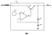
- the regulator circuit 2 divides the output voltage of the reference voltage source 6 for generating the reference voltage, the error amplifier 7, the output transistor 8 and the regulator circuit 2 at a predetermined voltage ratio, and the error amplifier 7 is divided. Resistance elements 9 and 10 for feedback to
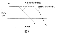
- the regulator circuit 2 has an open loop frequency characteristic as shown in FIG. 3, and the frequency characteristic changes depending on the presence or absence of the external capacitor 3. As a result, the system is kept stable when the external capacitor 3 is present, but becomes unstable when the external capacitor 3 is not present. In the regulator circuit 2, when the external capacitor 3 is provided, the output voltage becomes stable as shown in FIG. On the other hand, the regulator circuit 2 oscillates when the external capacitor 3 disappears due to disconnection or the like, and the output voltage vibrates greatly as shown in FIG.
- the oscillation of the output voltage of the regulator circuit 2 is detected by using the oscillation detector 4.
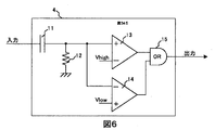
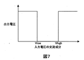
- the oscillation detector 4 includes a capacitor 11 and a resistor 12 that form a high-pass filter that removes a DC component of the input, and a comparator that outputs a high level when the output of the high-pass filter is higher than the voltage Vhigh. 13, a comparator 14 that outputs a high level when the output of the high-pass filter is smaller than the voltage Vlow, and a logic gate 15 that obtains the logical sum of the comparator 13 and the comparator 14. That is, the oscillation detector 4 outputs a high level when the AC component of the input voltage becomes larger than the voltage Vhigh or becomes smaller than the voltage Vlow as shown in FIG. 7.
- the input voltage of the oscillation detector 4 may be the voltage Vc in FIG. 2 or the internal voltage of the error amplifier 7.
- the purpose of the oscillation detector 4 is to detect the oscillation state of the regulator circuit 2, and when the regulator circuit 2 oscillates, all the voltages forming the feedback system oscillate. Therefore, the input voltage of the oscillation detector 4 may be the output voltage of the regulator circuit 2, the voltage Vc in FIG. 2, or the internal voltage of the error amplifier 7.
- the presence or absence of a disconnection failure of the external capacitor 3 can be detected by detecting the oscillation state of the regulator circuit 2. Therefore, it is possible to passively detect the presence or absence of the disconnection failure of the external capacitor 3 without affecting the operation of the regulator circuit 2. That is, as shown in FIG. 4, the operation of the regulator circuit 2 has almost no change in the output voltage at the time of diagnosis, and the change in the output voltage of the regulator circuit 2 and the increase in noise can be suppressed. Therefore, it is possible to connect to the regulator circuit 2 an electronic circuit that is weak against fluctuations in the power supply of the regulator circuit 2 or an electronic circuit that is easily affected by noise.
- the failure determination section 5 outputs a failure signal when the output of the oscillation detector 4 continues to detect the oscillation state of the regulator circuit for a predetermined time or longer.
- the output voltage of the regulator circuit 2 is constantly oscillated.
- the output voltage of the regulator circuit 2 may temporarily change due to a sudden change in the load current of the regulator circuit 2 or a change in the external voltage.
- the oscillation detector 4 outputs the high level when the oscillation of the regulator circuit 2 is detected. However, the oscillation detector 4 may output the low level when the oscillation is detected.
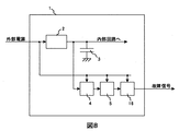
- FIG. 8 shows the configuration of the electronic device of the second embodiment. Note that the description of the same configuration as the first embodiment is omitted.
- the electronic device of this embodiment is basically the same as the electronic device of the first embodiment, but an output circuit 16 for outputting a failure signal to the host system is added. By doing so, it becomes possible to inform the host system of a failure of the electronic device 1, and it is possible to prevent the host system from entering a fatal failure mode due to a failure due to the failure of the electronic device 1 due to the host system.
- an external power supply (input voltage of the regulator circuit 2) was used as the power supply of the oscillation detector 4.
- the oscillation detector 4 is supplied with power from the external power source, and therefore the oscillation detector 4 operates stably. To be able to do. If the power supply of the oscillation detector 4 is supplied from the output voltage of the regulator 2, the output voltage of the regulator circuit 2 greatly oscillates due to the failure of the external capacitor 3, and as a result, the power supply voltage of the oscillation detector 4 is increased. May vibrate significantly and the oscillation detector 4 may malfunction, but this can be prevented in this embodiment.
- an external power supply was used as the power supply for the failure determination unit 5.
- the power of the failure determination unit 5 is supplied from the external power supply and the failure determination unit 5 operates stably. to enable. If the power of the failure determination unit 5 is supplied from the output voltage of the regulator 2, the output voltage of the regulator circuit 2 greatly vibrates due to the failure of the external capacitor 3, and as a result, the power supply voltage of the failure determination unit 5 is increased. May vibrate greatly and the failure determination unit 5 may malfunction, but this can be prevented in this embodiment.
- an external power supply was used as the power supply for the output circuit 16.
- the power supply of the output circuit 16 is supplied from the external power supply and the output circuit 16 can operate stably. To do. If the power supply of the output circuit 16 is supplied from the output voltage of the regulator 2, the output voltage of the regulator circuit 2 greatly vibrates due to the failure of the external capacitor 3, and as a result, the power supply voltage of the output circuit 16 becomes large. The output circuit 16 may vibrate and malfunction, but this can be prevented in the present embodiment.
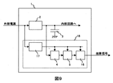
- FIGS. 9 is a configuration of the electronic device of the third embodiment
- FIG. 10 is a configuration of the second regulator circuit 17
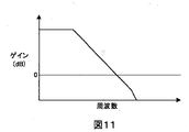
- FIG. 11 is a frequency characteristic of the open loop gain of the second regulator circuit. Note that the description of the same configuration as the first embodiment is omitted.
- the electronic device of this embodiment is basically the same as the electronic device of the first embodiment, but a second regulator circuit 17 is added, and the output voltage of this second regulator circuit is detected by oscillation detection 4 and failure judgment. It was used as a power source for the section 5 and the output circuit 16. It is more preferable to integrate the second regulator circuit 17, the oscillation detector 4, the failure determination unit 5, and the output circuit 16 in one LSI 18 in terms of downsizing.
- the second regulator circuit 17 divides the output voltage of the reference voltage source 19 that generates the reference voltage, the error amplifier 22, the output transistor 21, and the regulator circuit at a predetermined voltage ratio, and the error amplifier 22.
- the resistance elements 23 and 24 for feedback to the phase compensation capacitor 20 for stabilizing the feedback system are provided.
- the phase compensation capacitor 20 is provided with the open loop frequency characteristic shown in FIG. 11 to stabilize the feedback system. Therefore, since the second regulator circuit does not require a large-capacity capacitor at the output terminal, an external capacitor is not required, and it can be integrated in an LSI.
- the regulator having this configuration cannot increase the output current and can drive only a small-scale circuit, all the circuit elements constituting the regulator can be integrated, so that the reliability can be made extremely high. That is, in the third embodiment, by adding the second regulator 17, it becomes possible to supply more stable power to the oscillation detection 4, the failure determination unit 5, and the output circuit 16. As a result, the present embodiment ensures highly reliable and stable operation of the oscillation detection 4, the failure determination unit 5, and the output circuit 16. According to this embodiment, the failure diagnosis of the external capacitor 3 can be performed more reliably. This is because by providing the second regulator 17, a stable power supply voltage can be supplied to the oscillation detection 4, the failure determination unit 5, and the output circuit 16 even when the voltage of the external power supply fluctuates. Further, by providing the second regulator circuit 17, even if the external capacitor 3 has a short circuit failure, it is possible to stably operate the oscillation detection 4, the failure determination unit 5, and the output circuit 16.
- the output voltage of the second regulator circuit 17 is lower than the voltage of the regulator circuit 2, it is possible to increase the stability of the output voltage of the second regulator circuit 17 against the fluctuation of the external power supply. is there.
- the second regulator circuit 17, the oscillation detector 4, the failure determination unit 5, and the output circuit 16 are integrated.
- the mutual wiring of the output circuit 16 can be arranged on an LSI which can be connected with high reliability. As a result, a more stable diagnosis operation of the external capacitor 3 becomes possible.
- a physical quantity measuring device that measures at least one of physical quantities such as fluid flow rate, pressure, humidity, and temperature can be cited.
Landscapes
- Engineering & Computer Science (AREA)
- Physics & Mathematics (AREA)
- General Physics & Mathematics (AREA)
- Electromagnetism (AREA)
- Radar, Positioning & Navigation (AREA)
- Automation & Control Theory (AREA)
- Continuous-Control Power Sources That Use Transistors (AREA)
- Oscillators With Electromechanical Resonators (AREA)
Abstract
従来の電子装置ではレギュレータ回路の出力端子に付加される外部コンデンサの断線診断を受動的に行うことが困難であった。 本実施例の電子装置は外部から供給される外部電源を入力として一定電圧を出力するレギュレータ回路2と、レギュレータ回路2の出力端子に外部部品として接続される外部コンデンサ3と、レギュレータ回路2の出力電圧の発振状態を検出する発振検出器4と、発振検出器4が前記レギュレータ回路の発振状態を検出した場合に故障信号を出力する故障判定部5により構成される。
Description
本発明は出力端子に外部コンデンサを付加するレギュレータ回路を有する電子装置に係り、特に、前記外部コンデンサの断線故障を検出できる電子装置に関する。
レギュレータ回路の出力端子に付加される外部コンデンサの断線故障の診断方法の例として、特許文献1に記載された技術がある。特許文献1では、レギュレータ回路の出力電圧を意図的に変化させ、この出力電圧の変化によって生じるレギュレータ回路の出力電流が外部コンデンサの有無によって変化することを利用して、外部コンデンサの断線故障を診断することが開示されている。
特許文献1では外部コンデンサの断線の有無を検出するために、レギュレータ回路の出力電圧を意図的に変化させる必要があった。この為、電源電圧の変動に弱い回路に使用する場合には、回路動作を一時的に休止させてから外部コンデンサの断線の有無を検出する必要があった。この為、上記従来技術の適用範囲は限られたものであった。
本発明は上記事情に鑑みてなされたものであり、その目的は外部コンデンサの断線診断を受動的に行うことで、レギュレータ回路の出力電圧を常に安定な状態に保ち、レギュレータ回路から供給を受ける各回路の動作を休止させずに動作可能にする電子装置を提供することにある。
上記課題を解決するために、本発明における電子装置では出力端子に外部コンデンサが接続されるレギュレータ回路の発振状態を検出する発振検出器と、前記発振検出器が前記レギュレータ回路の発振状態を検出した場合に故障信号を出力する故障判定部と、を配置した。
本発明によれば、レギュレータ回路の出力端子に付加される外部コンデンサの断線故障を受動的に診断できるので、よりより広範な回路構成、特に、電源変動の影響を受けやすい回路構成にも適用できる電子装置を提供することが可能となる。
以下、本発明の実施の形態について、図面を参照して説明する。なお、各実施例は、矛盾しない限り組み合わせ可能である。
[第1の実施例]
まず、本発明の第1の実施例を図1から図7により説明する。なお、図1は第1の実施例の電子装置の構成、図2はレギュレータ回路2の構成、図3はレギュレータ回路2のオープンループの周波数特性、図4は正常時のレギュレータ回路の出力電圧波形、図5は外部コンデンサ3が断線した場合のレギュレータ回路の出力電圧波形、図6は発振検出器4の構成、図7は発振検出器4の入出力特性である。
まず、本発明の第1の実施例を図1から図7により説明する。なお、図1は第1の実施例の電子装置の構成、図2はレギュレータ回路2の構成、図3はレギュレータ回路2のオープンループの周波数特性、図4は正常時のレギュレータ回路の出力電圧波形、図5は外部コンデンサ3が断線した場合のレギュレータ回路の出力電圧波形、図6は発振検出器4の構成、図7は発振検出器4の入出力特性である。
本実施例の電子装置1は、外部から供給される外部電源を入力として一定電圧を出力するレギュレータ回路2と、レギュレータ回路2の出力端子に外部部品として接続される外部コンデンサ3と、レギュレータ回路2の出力電圧の発振状態を検出する発振検出器4と、発振検出器4がレギュレータ回路2の発振状態を検出した場合に故障信号を出力する故障判定部5と、を備える。
図2に示す様に、レギュレータ回路2は、基準電圧を発生させる基準電圧源6と、誤差増幅器7と、出力トランジスタ8と、レギュレータ回路2の出力電圧を所定の電圧比で分圧し誤差増幅器7へフィードバックする抵抗素子9、10を備える。
また、レギュレータ回路2は、図3に示す様なオープンループの周波数特性を持ち、外部コンデンサ3の有無により周波数特性が変化する。この結果、外部コンデンサ3がある場合には系を安定に保つが、外部コンデンサ3が無い場合には系は不安定になる。レギュレータ回路2は、外部コンデンサ3が有る場合は図4に示す様に出力電圧は安定する。一方で、レギュレータ回路2は、外部コンデンサ3が断線などにより無くなると発振して図5に示す様に出力電圧は大きく振動する。
本実施例では、このレギュレータ回路2の出力電圧の振動を発振検出器4を用いて検出する。発振検出器4は、図6に示す様に、入力の直流成分を除去するハイパスフィルタを構成するコンデンサ11と抵抗12と、ハイパスフィルタの出力が電圧Vhighより大きい場合にハイレベルを出力する比較器13と、ハイパスフィルタの出力が電圧Vlowより小さい場合にハイレベルを出力する比較器14と、比較器13と比較器14の論理和を求める論理ゲート15を備え得る。つまり、発振検出器4は、図7に示す様に入力電圧の交流成分が電圧Vhighより大きくなるか電圧Vlowより小さいくなるとハイレベルを出力する。なお、発振検出器4の入力電圧は図2中の電圧Vcであっても良いし誤差増幅器7の内部電圧でも良い。発振検出器4の目的はレギュレータ回路2の発振状態を検出することであり、レギュレータ回路2が発振した状態ではフィードバック系を構成する全ての電圧が振動する。この為、発振検出器4の入力電圧はレギュレータ回路2の出力電圧でも、図2中の電圧Vcでも、誤差増幅器7の内部電圧でも良い。
本実施例では、レギュレータ回路2の発振状態を検出することで外部コンデンサ3の断線故障の有無を検出できるようにした。この為、レギュレータ回路2の動作に影響を与えること無く受動的に外部コンデンサ3の断線故障の有無を検出できる。つまり、レギュレータ回路2の動作は図4に示す様に、診断時の出力電圧の変動はほとんど無く、レギュレータ回路2の出力電圧の変動やノイズの増加を抑えることができる。この為、レギュレータ回路2の電源変動に弱い電子回路やノイズの影響を受けやす電子回路を、レギュレータ回路2に接続することができる。
また、故障判定部5は、発振検出器4の出力が所定の時間以上にわたって前記レギュレータ回路の発振状態を検出し続けた場合に故障信号を出力する様にするとより好ましい。
外部コンデンサ3が断線や故障により外部コンデンサ3の機能が失われた場合、定常的にレギュレータ回路2の出力電圧は定常的に発振状態になる。一方で、レギュレータ回路2の負荷電流の急変や外部電圧の変動などにより、レギュレータ回路2の出力電圧が一時的に変動することがある。発振検出器4の出力が所定の時間以上にわたって発振状態を示すハイレベルを示す場合に故障信号を出力することで、この一時的な変動による誤検出が生じ無い様にできる効果がある。
外部コンデンサ3が断線や故障により外部コンデンサ3の機能が失われた場合、定常的にレギュレータ回路2の出力電圧は定常的に発振状態になる。一方で、レギュレータ回路2の負荷電流の急変や外部電圧の変動などにより、レギュレータ回路2の出力電圧が一時的に変動することがある。発振検出器4の出力が所定の時間以上にわたって発振状態を示すハイレベルを示す場合に故障信号を出力することで、この一時的な変動による誤検出が生じ無い様にできる効果がある。
なお、本実施例では、発振検出器4がレギュレータ回路2の発信を検知した場合にハイレベルを出力する例を示しているが、発信を検知した場合にローレベルを出力する構成としてもよい。
[第2の実施例]
次に、本発明の第2の実施例である電子装置を図8により説明する。なお、図8は第2の実施例の電子装置の構成である。なお、第1の実施例と同様の構成については説明を省略する。
次に、本発明の第2の実施例である電子装置を図8により説明する。なお、図8は第2の実施例の電子装置の構成である。なお、第1の実施例と同様の構成については説明を省略する。
本実施例の電子装置は基本的には第1の実施例の電子装置と同じであるが、上位システムへ故障信号を出力する為の出力回路16を付加た。こうすることで、本電子装置1の故障を上位システムに伝えることが可能になり、上位システムにより本電子装置1の故障による不具合により上位システムが致命的な故障モードに成らない様にできる。
また、発振検出器4の電源に外部電源(レギュレータ回路2の入力電圧)を用いた。こうすることで、仮に外部コンデンサ3が故障してレギュレータ回路2の出力電圧が大きく振動したとしても、発振検出器4の電源は外部電源から供給されるため、発振検出器4は安定して動作することを可能にする。仮に、発振検出器4の電源をレギュレータ2の出力電圧から供給された場合には外部コンデンサ3が故障することでレギュレータ回路2の出力電圧が大きく振動し、この結果、発振検出器4の電源電圧が大きく振動し発振検出器4が誤動作する恐れがあるが本実施例ではこれを防ぐことができる。
また、故障判定部5の電源に外部電源を用いた。こうすることで、仮に外部コンデンサ3が故障してレギュレータ回路2の出力電圧が大きく振動したとしても、故障判定部5の電源は外部電源から供給され故障判定部5は安定して動作することを可能にする。仮に、故障判定部5の電源をレギュレータ2の出力電圧から供給された場合には外部コンデンサ3が故障することでレギュレータ回路2の出力電圧が大きく振動し、この結果、故障判定部5の電源電圧が大きく振動し故障判定部5が誤動作する恐れがあるが本実施例ではこれを防ぐことができる。
また、出力回路16の電源に外部電源を用いた。こうすることで、仮に外部コンデンサ3が故障してレギュレータ回路2の出力電圧が大きく振動したとしても、出力回路16の電源は外部電源から供給され出力回路16は安定して動作することを可能にする。仮に、出力回路16の電源をレギュレータ2の出力電圧から供給された場合には外部コンデンサ3が故障することでレギュレータ回路2の出力電圧が大きく振動し、この結果、出力回路16の電源電圧が大きく振動し出力回路16が誤動作する恐れがあるが本実施例ではこれを防ぐことができる。
[第3の実施例]
次に、本発明の第3の実施例である電子装置を図9から図11により説明する。なお、図9は第3の実施例の電子装置の構成、図10は第2レギュレータ回路17の構成、図11は第2レギュレータ回路のオープンループゲインの周波数特性である。なお、第1の実施例と同様の構成については説明を省略する。
次に、本発明の第3の実施例である電子装置を図9から図11により説明する。なお、図9は第3の実施例の電子装置の構成、図10は第2レギュレータ回路17の構成、図11は第2レギュレータ回路のオープンループゲインの周波数特性である。なお、第1の実施例と同様の構成については説明を省略する。
本実施例の電子装置は基本的には第1の実施例の電子装置と同じであるが、第2レギュレータ回路17を付加し、この第2のレギュレータ回路の出力電圧を発振検出4、故障判定部5、出力回路16の電源に用いた。第2レギュレータ回路17、発振検出器4、故障判定部5、出力回路16を1つのLSI18に集積化すると小型化の観点でより好ましい。
第2レギュレータ回路17は、図10に示す様に、基準電圧を発生させる基準電圧源19と誤差増幅器22と、出力トランジスタ21と、レギュレータ回路の出力電圧を所定の電圧比で分圧し誤差増幅器22へフィードバックする抵抗素子23、24と、フィードバック系の安定化を図る位相補償容量20を備える。第2レギュレータ回路17では位相補償容量20により図11に示すオープンループの周波数特性を持たせ、フィードバック系の安定化を図っている。この為、第2レギュレータ回路では出力端子に大容量のコンデンサを必要としないので、外部コンデンサは不要であり、LSIへの集積化も可能になる。
但し、この構成のレギュレータは出力電流を大きくできないので小規模な回路しか駆動できないが、レギュレータを構成する全ての回路素子を集積化できるので非常に信頼度を高くできる。つまり、第3の実施例では第2レギュレータ17を付加することで、発振検出4、故障判定部5、出力回路16へより安定な電源を供給することが可能となる。その結果、本実施例は、発振検出4、故障判定部5、出力回路16の高信頼な安定動作を確保した。本実施例によれば、外部コンデンサ3の故障診断をより確実に行えるようにできる。
これは、第2レギュレータ17を備えることにより、外部電源の電圧が変動した場合であっても、発振検出4、故障判定部5、出力回路16に安定な電源電圧を供給できるからである。また、第2レギュレータ回路17を設けることで、仮に外部コンデンサ3が短絡故障した場合であっても、発振検出4、故障判定部5、出力回路16を安定に動作させることが可能である。
更なる好例として、第2レギュレータ回路17の出力電圧をレギュレータ回路2の電圧よりも低電圧にすることで、外部電源の変動に対する第2レギュレータ回路17の出力電圧の安定度を高めることが可能である。
更なる好例として、第2レギュレータ回路17、発振検出器4、故障判定部5、出力回路16を1つのLSIに集積化することで、第2レギュレータ回路17、発振検出器4、故障判定部5、出力回路16の相互配線を高信頼度に接続できるLSI上に配置できる。
その結果、より安定した外部コンデンサ3の診断動作が可能となる。
その結果、より安定した外部コンデンサ3の診断動作が可能となる。
本実施例の電子装置の例としては種々考えられるが、例えば、流体の流量、圧力、湿度、温度といった物理量のうち少なくとも何れかひとつを測定する物理量測定装置が挙げられる。
1‥電子装置、2‥レギュレータ回路、3‥外部コンデンサ、4‥発振検出器、5‥故障判定部、6‥基準電圧源、7‥誤差増幅器、8‥出力トランジスタ、9‥抵抗素子、10‥抵抗素子、11‥コンデンサ、12‥抵抗、13‥比較器、14‥比較器、15‥論理ゲート、16‥出力回路、17‥第2レギュレータ回路、18‥LSI、19‥基準電圧源、20‥位相補償容量、21‥出力トランジスタ、22‥誤差増幅器、23‥抵抗素子、24‥抵抗素子
Claims (11)
- 出力端子に外部コンデンサが接続されるレギュレータ回路と、
前記レギュレータ回路の発振状態を検出する発振検出器と、を備える電子装置 - 前記発振検出器からの信号に基づき故障信号を出力する故障判定部を備える請求項2に記載の電子装置
- 前記故障判定部は、前記発振検出器が所定の時間以上にわたって前記レギュレータ回路の発振状態を検出し続けた場合に故障信号を出力する請求項2に記載の電子装置
- 前記レギュレータ回路の入力電圧を前記発振検出器の電源として用いる請求項1乃至3の何れかに記載の電子装置
- 第2のレギュレータ回路を備え、
前記第2のレギュレータ回路の出力電圧を前記発振検出器の電源として用いる請求項1乃至3の何れかに記載の電子装置 - 前記第2のレギュレータ回路の出力電圧は、前記レギュレータ回路の出力電圧よりも低電圧である請求項5に記載の電子装置
- 前記第2のレギュレータ回路および前記発振検出器を同一の半導体素子に集積化した請求項6に記載の電子装置
- 前記第2のレギュレータ回路の出力を電源として用いる故障信号出力回路を有する請求項6に記載の電子装置
- 前記第2のレギュレータ回路、前記発信検出器、前記故障判定部、前記故障判定部の出力を外部へ送信する出力回路、を同一の半導体素子に集積化した請求項7に記載の電子装置
- 前記第2のレギュレータ回路は、位相補償容量を備える請求項9に記載の電子装置
- 前記電子装置は、流体の物理量を測定する物理量測定装置である請求項10に記載の物理量測定装置。
Priority Applications (3)
| Application Number | Priority Date | Filing Date | Title |
|---|---|---|---|
| DE112019004911.9T DE112019004911T5 (de) | 2018-11-12 | 2019-10-23 | Elektronische einrichtung |
| CN201980064386.3A CN113168197A (zh) | 2018-11-12 | 2019-10-23 | 电子装置 |
| US17/288,974 US12174649B2 (en) | 2018-11-12 | 2019-10-23 | Electronic device |
Applications Claiming Priority (2)
| Application Number | Priority Date | Filing Date | Title |
|---|---|---|---|
| JP2018211897A JP7121637B2 (ja) | 2018-11-12 | 2018-11-12 | 電子装置 |
| JP2018-211897 | 2018-11-12 |
Publications (1)
| Publication Number | Publication Date |
|---|---|
| WO2020100537A1 true WO2020100537A1 (ja) | 2020-05-22 |
Family
ID=70732001
Family Applications (1)
| Application Number | Title | Priority Date | Filing Date |
|---|---|---|---|
| PCT/JP2019/041445 Ceased WO2020100537A1 (ja) | 2018-11-12 | 2019-10-23 | 電子装置 |
Country Status (5)
| Country | Link |
|---|---|
| US (1) | US12174649B2 (ja) |
| JP (1) | JP7121637B2 (ja) |
| CN (1) | CN113168197A (ja) |
| DE (1) | DE112019004911T5 (ja) |
| WO (1) | WO2020100537A1 (ja) |
Families Citing this family (1)
| Publication number | Priority date | Publication date | Assignee | Title |
|---|---|---|---|---|
| KR102863074B1 (ko) | 2021-07-28 | 2025-09-19 | 삼성전자주식회사 | 발진 검출기 및 이의 동작 방법 |
Citations (3)
| Publication number | Priority date | Publication date | Assignee | Title |
|---|---|---|---|---|
| JPH06319265A (ja) * | 1993-04-30 | 1994-11-15 | Sankyo Seiki Mfg Co Ltd | インバータ装置 |
| JP2006099500A (ja) * | 2004-09-30 | 2006-04-13 | Mitsumi Electric Co Ltd | レギュレータ回路 |
| JP2007252012A (ja) * | 2006-03-13 | 2007-09-27 | Pentax Corp | レギュレータ破損防止システム |
Family Cites Families (11)
| Publication number | Priority date | Publication date | Assignee | Title |
|---|---|---|---|---|
| JPH09229986A (ja) * | 1996-02-21 | 1997-09-05 | Toyo Commun Equip Co Ltd | 電源平滑化コンデンサの故障検出装置 |
| JP3732173B2 (ja) * | 2002-11-18 | 2006-01-05 | ローム株式会社 | 電源装置及びこれを用いた液晶表示装置 |
| JP2007252102A (ja) * | 2006-03-16 | 2007-09-27 | Yaskawa Electric Corp | インバータ制御装置 |
| CN101656327A (zh) * | 2008-08-19 | 2010-02-24 | 昂扬 | 即充即用型充电电池 |
| CN101546205B (zh) | 2008-03-28 | 2011-05-04 | 瑞鼎科技股份有限公司 | 电源管理电路及其频率补偿方法 |
| CN201666890U (zh) * | 2009-05-05 | 2010-12-08 | 罗琳 | 金属残留监测装置 |
| JP5715587B2 (ja) * | 2012-03-21 | 2015-05-07 | 株式会社東芝 | レギュレータ |
| JP5898589B2 (ja) * | 2012-08-10 | 2016-04-06 | 株式会社東芝 | Dc−dcコンバータの制御回路およびdc−dcコンバータ |
| CN106610683A (zh) | 2015-10-22 | 2017-05-03 | 湖南南车时代电动汽车股份有限公司 | 一种ldo电源电路 |
| JP6499056B2 (ja) * | 2015-10-28 | 2019-04-10 | 日立オートモティブシステムズ株式会社 | 車載用半導体装置 |
| JP6788962B2 (ja) * | 2015-11-19 | 2020-11-25 | セイコーエプソン株式会社 | 診断回路、電子回路、電子機器および移動体 |
-
2018
- 2018-11-12 JP JP2018211897A patent/JP7121637B2/ja active Active
-
2019
- 2019-10-23 CN CN201980064386.3A patent/CN113168197A/zh active Pending
- 2019-10-23 DE DE112019004911.9T patent/DE112019004911T5/de active Pending
- 2019-10-23 US US17/288,974 patent/US12174649B2/en active Active
- 2019-10-23 WO PCT/JP2019/041445 patent/WO2020100537A1/ja not_active Ceased
Patent Citations (3)
| Publication number | Priority date | Publication date | Assignee | Title |
|---|---|---|---|---|
| JPH06319265A (ja) * | 1993-04-30 | 1994-11-15 | Sankyo Seiki Mfg Co Ltd | インバータ装置 |
| JP2006099500A (ja) * | 2004-09-30 | 2006-04-13 | Mitsumi Electric Co Ltd | レギュレータ回路 |
| JP2007252012A (ja) * | 2006-03-13 | 2007-09-27 | Pentax Corp | レギュレータ破損防止システム |
Also Published As
| Publication number | Publication date |
|---|---|
| JP2020079972A (ja) | 2020-05-28 |
| US20210389787A1 (en) | 2021-12-16 |
| JP7121637B2 (ja) | 2022-08-18 |
| DE112019004911T5 (de) | 2021-06-10 |
| CN113168197A (zh) | 2021-07-23 |
| US12174649B2 (en) | 2024-12-24 |
Similar Documents
| Publication | Publication Date | Title |
|---|---|---|
| JP4296811B2 (ja) | 物理量センサ装置 | |
| EP3499335A1 (en) | Regulator circuit and semiconductor device, and power supply | |
| JP2004294442A (ja) | 故障検出を備えたエンジン速度センサ | |
| JP2019160011A (ja) | ボルテージレギュレータ | |
| JP5487568B2 (ja) | 半導体装置 | |
| KR100593116B1 (ko) | 리졸버 고장 진단 회로 | |
| CN111693759B (zh) | 电压检测器 | |
| US20110196628A1 (en) | Deterioration detection circuit | |
| JP2009277122A (ja) | 電源電圧監視回路 | |
| US6605929B2 (en) | Power supply noise sensor | |
| US9843256B2 (en) | Internal voltage generation circuit | |
| JP2013205085A (ja) | 半導体装置 | |
| JP7121637B2 (ja) | 電子装置 | |
| JP2017174116A (ja) | ボルテージレギュレータ | |
| CN108136442B (zh) | 压电致动器驱动电路 | |
| US20070064953A1 (en) | Speaker protection circuit | |
| CN111309091B (zh) | 半导体设备和包括半导体设备的半导体系统 | |
| JP2024060507A (ja) | 物理量出力回路 | |
| JP2008141612A (ja) | 負荷駆動装置の故障検出装置および負荷駆動用ic | |
| WO2023022022A1 (ja) | 半導体装置、車載装置 | |
| US20110018598A1 (en) | Pll circuit | |
| JP5466970B2 (ja) | 半導体集積回路 | |
| JP2009094553A (ja) | 増幅器 | |
| JP2007022432A (ja) | 負荷異常検出装置 | |
| JP3824620B2 (ja) | トルクセンサ |
Legal Events
| Date | Code | Title | Description |
|---|---|---|---|
| 121 | Ep: the epo has been informed by wipo that ep was designated in this application |
Ref document number: 19885230 Country of ref document: EP Kind code of ref document: A1 |
|
| 122 | Ep: pct application non-entry in european phase |
Ref document number: 19885230 Country of ref document: EP Kind code of ref document: A1 |