WO2020100449A1 - マイクロled表示装置及びマイクロled表示装置の配線方法 - Google Patents
マイクロled表示装置及びマイクロled表示装置の配線方法 Download PDFInfo
- Publication number
- WO2020100449A1 WO2020100449A1 PCT/JP2019/038231 JP2019038231W WO2020100449A1 WO 2020100449 A1 WO2020100449 A1 WO 2020100449A1 JP 2019038231 W JP2019038231 W JP 2019038231W WO 2020100449 A1 WO2020100449 A1 WO 2020100449A1
- Authority
- WO
- WIPO (PCT)
- Prior art keywords
- micro led
- semiconductor layer
- display device
- led display
- micro
- Prior art date
- Legal status (The legal status is an assumption and is not a legal conclusion. Google has not performed a legal analysis and makes no representation as to the accuracy of the status listed.)
- Ceased
Links
Images



Classifications
-
- G—PHYSICS
- G09—EDUCATION; CRYPTOGRAPHY; DISPLAY; ADVERTISING; SEALS
- G09F—DISPLAYING; ADVERTISING; SIGNS; LABELS OR NAME-PLATES; SEALS
- G09F9/00—Indicating arrangements for variable information in which the information is built-up on a support by selection or combination of individual elements
-
- G—PHYSICS
- G09—EDUCATION; CRYPTOGRAPHY; DISPLAY; ADVERTISING; SEALS
- G09F—DISPLAYING; ADVERTISING; SIGNS; LABELS OR NAME-PLATES; SEALS
- G09F9/00—Indicating arrangements for variable information in which the information is built-up on a support by selection or combination of individual elements
- G09F9/30—Indicating arrangements for variable information in which the information is built-up on a support by selection or combination of individual elements in which the desired character or characters are formed by combining individual elements
-
- H—ELECTRICITY
- H10—SEMICONDUCTOR DEVICES; ELECTRIC SOLID-STATE DEVICES NOT OTHERWISE PROVIDED FOR
- H10H—INORGANIC LIGHT-EMITTING SEMICONDUCTOR DEVICES HAVING POTENTIAL BARRIERS
- H10H20/00—Individual inorganic light-emitting semiconductor devices having potential barriers, e.g. light-emitting diodes [LED]
- H10H20/80—Constructional details
- H10H20/85—Packages
- H10H20/857—Interconnections, e.g. lead-frames, bond wires or solder balls
Definitions
- the present invention relates to a micro LED display device and a wiring method for the micro LED display device.
- a display device using a light emitting diode is conventionally known.
- the micro LED technology is a technology based on the premise that the size of a single LED is miniaturized to a level of several ⁇ m to several tens ⁇ m.
- a display unit for example, a pixel
- a display device can be made lighter, thinner, shorter, smaller, higher in brightness, higher in definition, and more energy-saving, and in addition to the miniaturized micro LED. It is attracting attention as a material that can realize next-generation displays such as a transparent display having a transparent substrate and a flexible display having a substrate on which a micro LED is mounted as a flexible substrate.
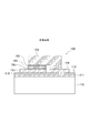
- FIG. 1 shows a conventional technique in which a single micro LED is mounted on a wiring board by flip chip mounting.
- the matrix wiring is composed of, for example, a lower-layer n-electrode wiring 111 extending in a direction orthogonal to each other and an upper-layer p-electrode wiring 113 formed on the lower-layer n-electrode wiring 111 via an insulating film 112.
- the flip-chip mounted micro LED 100 includes an n-type semiconductor layer 101, an active layer (light-emitting layer) 102, and a p-type semiconductor layer 103, and the n-type semiconductor layer 101 is an n-th layer under the insulating film 112 via a through hole.
- the p-type semiconductor layer 103 is connected to the n-electrode 104 connected to the electrode wiring 111, and is connected to the upper-layer p-electrode wiring 113 wired on the insulating film 112 via the p-electrode 105.
- the n-electrode 104 and the p-electrode 105 are provided on the same surface side of the micro LED 100, the light-emitting portion can be obtained at least in the area overlapping with the p-electrode 105. For this reason, when the size of the micro LED 100 becomes smaller, the area of the n-electrode 104 cannot be reduced accordingly, so that the area occupied by the n-electrode 104 with respect to the size of the micro LED 100 becomes larger, and the micro LED 100 becomes larger. There is a problem in that the light emission efficiency with respect to the dimension is reduced.
- the present invention has been proposed to address such a problem. That is, in a micro LED display device in which micro LEDs are arranged in a matrix and matrix wirings are respectively connected to the p-type semiconductor layer and the n-type semiconductor layer, the light emission efficiency with respect to the size of the micro LEDs is not reduced.
- the problem is to improve the productivity of the micro LED display device by efficiently forming the matrix wiring connected to the micro LED.
- a micro LED display device in which a plurality of micro LEDs are arranged in a matrix in an X direction which is one direction along a surface of a substrate and a Y direction along a surface of the substrate which intersects the X direction, the micro LED being formed on the substrate.
- a plurality of first electrode wirings extending in the X direction and arranged in parallel in the Y direction, and a first semiconductor layer, a light emitting layer, and a second semiconductor layer are stacked along the Z direction intersecting the surface.
- a micro LED having a vertical structure, in which the first semiconductor layer is connected to the first electrode wiring, and a light emitting region of the micro LED formed on the substrate on which the first electrode wiring is formed.
- a micro LED display device comprising:
- a micro LED display device having such characteristics is a micro LED in which micro LEDs are arranged in a matrix and matrix wirings are respectively connected to a p-type semiconductor layer (first semiconductor layer) and an n-type semiconductor layer (second semiconductor layer).
- matrix wiring can be performed without reducing the light emission efficiency with respect to the size of the micro LED. Further, by efficiently forming the matrix wiring connected to the micro LED, the productivity of the micro LED display device can be improved.
- FIG. 1 It is an explanatory view explaining a micro LED display device by flip chip mounting of the prior art. It is explanatory drawing which showed the structural example of the micro LED display apparatus which concerns on the 1st Embodiment of this invention. It is explanatory drawing which showed the wiring structure of the micro LED simple substance of the micro LED display apparatus in FIG. It is explanatory drawing which showed the structural example of the micro LED display apparatus which concerns on the 2nd Embodiment of this invention. It is explanatory drawing which showed the wiring structure of the micro LED simple substance of the micro LED display apparatus in FIG. It is explanatory drawing (formation of 1st electrode wiring and the mounting process of micro LED) explaining an example of the wiring method of the micro LED display apparatus which concerns on embodiment of this invention.
- FIG. 1st electrode wiring and the mounting process of micro LED explaining an example of the wiring method of the micro LED display apparatus which concerns on embodiment of this invention.
- FIG. 6 is an explanatory view (insulating film formation and recess formation step) for explaining an example of a wiring method of the micro LED display device according to the embodiment of the present invention. It is explanatory drawing (2nd electrode wiring formation process) explaining an example of the wiring method of the micro LED display apparatus which concerns on embodiment of this invention. It is explanatory drawing which showed the example of the color display of the micro LED display apparatus which concerns on embodiment of this invention.
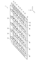
- a plurality of micro LEDs 10 are arranged in the X direction, which is one direction along the surface of the substrate 20, and along the surface of the substrate intersecting the X direction. It is arranged in a matrix in the Y direction.
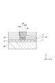
- the single micro LED 10 has the first semiconductor layer 11, the light emitting layer 12, and the second semiconductor layer 13 stacked along the Z direction intersecting the surface (XY plane) of the substrate 20. It has a vertical structure.
- the first electrode wiring 21 and the second electrode wiring 22 are arranged on the substrate 20 so as to intersect three-dimensionally to form a matrix wiring.
- the first electrode wirings 21 are formed on the substrate 20 directly or via an insulating film or the like, and the individual first electrode wirings 21 are extended in the X direction shown in the drawing, and the plurality of first electrode wirings 21 are formed. Are arranged in parallel in the illustrated Y direction.
- the second electrode wiring 22 is formed on the insulating film 23 formed on the substrate 20 on which the first electrode wiring 21 is formed, and each second electrode wiring 22 is extended in the Y direction shown in the drawing.
- the plurality of second electrode wirings 22 are arranged in parallel in the X direction shown.
- the first semiconductor layer 11 of the micro LED 10 is connected to the first electrode wiring 21, and the side surface 13A (YZ surface) of the second semiconductor layer 13 of the micro LED 10 is connected to the second electrode wiring 22. ing.
- the upper surface 13B of the micro LED 10 serving as the light emitting region is exposed from the opening of the insulating film 23, and no electrode connecting portion is formed on the upper surface 13B.
- the recess 23A is formed in the insulating film 23, the side surface 13A of the second semiconductor layer 13 of the micro LED 10 is exposed in the recess 23A, and the second electrode wiring 22 is formed in the recess 23A. Then, the second electrode wiring 22 is connected to the side surface 13A of the second semiconductor layer 13.
- the present invention is not limited to this, and the side surface 13A of the second semiconductor layer 13 is exposed on the insulating film 23 by forming the insulating film 23 to be thinner than the vertical thickness of the vertical type micro LED 10, for example. Then, by forming the second electrode wiring 22 on the insulating film 23, the second electrode wiring 22 may be connected to the side surface 13A of the second semiconductor layer 13.
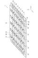
- FIGS. 4 and 5 show a micro LED display device 1 according to another embodiment.
- the example shown in FIGS. 4 and 5 has a configuration in which the second electrode wiring 22 has an opening in the light emitting region therein, and the micro LED 10 is arranged in the opening, and The points are the same as the examples shown in FIGS. 2 and 3.
- the second electrode wiring 22 is connected to the side surface 13A of the second semiconductor layer 13 of the micro LED 10 on the four surfaces inside the opening provided in the second electrode wiring 22.
- the first semiconductor layer 11 in the micro LED 10 is, for example, p-GaN
- the second semiconductor layer 13 is n-GaN
- the light emitting layer 12 is an active layer having an MQW (Multiple Quantum Well) structure.
- the material of the micro LED 10 is not particularly limited, and various semiconductor materials capable of forming the vertical micro LED 10 can be used.
- first electrode wiring 21 and the second electrode wiring 22 a conductive metal such as Al, Au, Ag, Cu can be used. Further, the first electrode wiring 21 and the second electrode wiring 22 can be formed as a single layer or a multilayer film made of a conductive material such as Ni.
- the insulating layer 23 can be made of a resin material such as epoxy, polyimide or silicone, or an inorganic material such as alumina or silica.
- the substrate 20 may be made of any material, such as glass or resin, as long as it can insulate the first electrode wiring 21, and if an insulating coating is formed on the underlying layer of the first electrode wiring 21, Further, any material including a conductive material such as metal can be used. Further, the substrate 20 is not limited to a rigid plate body, and may be a flexible film body or the like.
- an electrode connecting portion is provided on the upper surface 13B of the second semiconductor layer 13 which is a light emitting region in each of the micro LEDs 10 arranged in a matrix on the substrate 20. Since it does not exist, it is possible to drive the plurality of micro LEDs 10 for display without lowering the light emission efficiency with respect to the size of the micro LEDs 10.
- the upper surface 13B of each individual micro LED 10 is exposed from the opening of the insulating film 23 or the second electrode wiring 22 and there is nothing that blocks the upper surface 13B which is a light emitting region. It is possible to emit ultraviolet rays having a desired wavelength without being restricted by the transmission wavelength.
- the formation of the micro LED display device 1 shown here includes the step of forming the first electrode wiring shown in FIGS. 6A and 6B, the step of mounting the micro LED shown in FIG.
- the steps of forming the insulating film shown in a) to (c) and the step of forming the second electrode wiring shown in FIG. 8 are included, the method is not particularly limited to this method.
- a plurality of first electrode wirings are formed on the flat plate-shaped or film-shaped substrate 20 prepared as shown in FIG. 6A. 21 are formed in parallel.
- a metal material such as Al or Cu is formed on the substrate 20 by a film forming technique such as sputtering, plating, or vapor deposition to a thickness of, for example, about 500 nm, and then a photolithographic technique or the like is used to show X in the drawing.
- the plurality of first electrode wirings 21 extending in the direction and arranged in parallel in the Y direction in the drawing are patterned.
- the micro LED 10 that has been formed in advance and divided into a size of several ⁇ n to several tens ⁇ m ⁇ is attached to the first electrode wiring 21. 21 are arranged in a matrix. Here, the first semiconductor layer 11 of the micro LED 10 is connected on the first electrode wiring 21.
- the insulating film 23 which is a photosensitive resin film is formed as shown in FIG. 7A.
- the insulating film 23 is formed by coating or the like on the substrate 20 on which the first electrode wiring 21 is formed.
- the insulating film 23 has a thickness of about 8 to 9 ⁇ m, and the upper portion of the micro LED 10 is projected from the surface of the insulating film 23. This is to prevent the insulating film 23 from covering the upper surface 13B of the micro LED, which is the light emitting region, whereby the insulating film 23 is formed so that the light emitting region of the micro LED 10 is opened.
- the exposure mask 30 is installed so that the opening 31 is aligned with the side surface 13A of the micro LED 10, and exposure, development, and etching are performed by a photolithography process.
- An insulating film 23 having a pattern of recesses 23A as shown in FIG. 7C is formed.
- the side surface 13A of the second semiconductor layer 13 in the micro LED 10 is exposed in the recess 23A.
- the size of the recess 23A can be set to have a width of about 1 to 5 ⁇ m and a depth of about 2 to 3 ⁇ m.
- the depth of the recess 23A needs to be set so that the light emitting layer 12 of the micro LED 10 is not exposed.
- a film forming mask 40 is formed.
- the film forming mask 40 is a mask layer in which an opening 41 corresponding to the pattern of the recess 23A is formed, and is removed after the layer of the second electrode wiring 22 is formed in the recess 23A by sputtering or vapor deposition. It is a thing.
- the micro LED display device 1 is completed by removing the film forming mask 40 after forming the second electrode wiring 22.
- FIG. 9 shows a configuration example when the micro LED display device 1 is used as a color display device.
- the light wavelength conversion unit 50 is provided on the light emission side of the micro LED 10 that emits ultraviolet rays UV.
- the light wavelength conversion unit 50 emits visible light excited by the ultraviolet UV emitted from the micro LED 10, and emits a phosphor 51 that emits red light by the ultraviolet UV and a green light by the ultraviolet UV. And a phosphor 53 that emits blue light by ultraviolet UV.
- Each phosphor 51, 52, 53 is partitioned by a partition wall 54, and a support 55 that transmits ultraviolet rays is provided on the micro LED 10 side of the phosphors 51, 52, 53.
- a filter layer 56 that transmits visible light and absorbs ultraviolet light is provided on the light emission side.
- Micro LED display device 10: Micro LED, 11: first semiconductor layer, 12: light emitting layer, 13: second semiconductor layer, 13A: side surface, 13B: top surface, 20: substrate, 21: first electrode wiring, 22: second electrode wiring, 23: insulating film, 30: exposure mask, 31: aperture, 40: mask for film formation, 41: opening, 50: light wavelength conversion part, 51, 52, 53: phosphor, 54: partition wall, 55: support, 56: filter layer
Landscapes
- Physics & Mathematics (AREA)
- General Physics & Mathematics (AREA)
- Engineering & Computer Science (AREA)
- Theoretical Computer Science (AREA)
- Led Device Packages (AREA)
- Devices For Indicating Variable Information By Combining Individual Elements (AREA)
Abstract
マイクロLEDをマトリクス状に配置してp型半導体層とn型半導体層にマトリクス配線をそれぞれ接続するマイクロLED表示装置において、マイクロLEDの寸法に対する光出射効率を低下させないようにする。マイクロLED表示装置は、基板上に形成され、X方向に延設されると共にY方向に並列される複数の第1電極配線と、基板の表面に交差するZ方向に沿って第1半導体層と発光層と第2半導体層が積層された縦型構造を備え、第1半導体層が第1電極配線上に接続されるマイクロLEDと、第1電極配線が形成された基板上に形成され、マイクロLEDの光出射領域を開口した絶縁膜と、第2半導体層の側面に接続されるように絶縁膜上に形成され、Y方向に延設されると共にX方向に並列される複数の第2電極配線とを備える。
Description
本発明は、マイクロLED表示装置及びマイクロLED表示装置の配線方法に関するものである。
発光ダイオード(LED)を用いる表示装置(ディスプレイ)は、従来から知られている。これに対して、マイクロLED技術は、LED単体の大きさを数μm~数十μmのレベルまで微細化することを前提とした技術であり、このように微細化されたLED(以下、マイクロLED)を表示単位(例えば、画素)とする表示装置は、表示装置の軽薄短小化、高輝度化、高精細化、省エネ化等が可能になることに加えて、微細化したマイクロLED以外の部分を透明にした透明ディスプレイやマイクロLEDを実装する基板をフレキシブル基板にしたフレキシブルディスプレイなどの次世代ディスプレイを実現できるものとして注目されている。
マイクロLED表示装置を量産化するためには、幾つかの解決すべき課題があると言われているが、その一つが、マイクロLEDの実装・配線を如何に低コスト且つ効率的に行うかの問題である。従来、アレイ化したLEDの実装には、フリップチップ実装が行われているが、マイクロLED表示装置においても、ワイヤーボンディングなどに比べて実装面積を小さくすることができるフリップチップ実装を採用することが提案されている(下記特許文献1参照)。
図1は、フリップチップ実装によって単体のマイクロLEDを配線基板上に実装した状態の従来技術を示している。マイクロLED100をマトリクス状に複数配列した表示装置を構成するためには、配列した複数のマイクロLED100を接続するためのマトリクス配線を基板110上形成することが必要になる。マトリクス配線は、例えば、互いに直交する方向に延設される下層のn電極配線111と、絶縁膜112を介して下層n電極配線111の上に形成される上層のp電極配線113とによって構成される。
フリップチップ実装されるマイクロLED100は、n型半導体層101と活性層(発光層)102とp型半導体層103を備え、n型半導体層101が、絶縁膜112のスルーホールを介して下層のn電極配線111に接続されるn電極104に接続されており、p型半導体層103が、絶縁膜112上に配線される上層のp電極配線113にp電極105を介して接続されている。
このような従来技術では、マイクロLED100の同じ面側に、n電極104とp電極105が設けられることになるので、少なくともp電極105と重なる面積分しか発光部分が得られないことになる。このため、マイクロLED100の寸法がより微小になった場合に、それに応じてn電極104の面積を小さくすることができなくなるので、マイクロLED100の寸法に対するn電極104の占有面積が大きくなり、マイクロLED100の寸法に対する光出射効率が低下してしまうという問題が生じる。
本発明は、このような問題に対処するために提案されたものである。すなわち、マイクロLEDをマトリクス状に配置してp型半導体層とn型半導体層にマトリクス配線をそれぞれ接続するマイクロLED表示装置において、マイクロLEDの寸法に対する光出射効率を低下させないようにすること、また、マイクロLEDに接続するマトリクス配線を効率良く形成することで、マイクロLED表示装置の生産性向上を図ること、などを課題としている。
このような課題を解決するために、本発明は、以下の構成を具備するものである。
複数のマイクロLEDを基板の表面に沿った一方向であるX方向とそれに交差する基板の表面に沿ったY方向にマトリクス状に配列したマイクロLED表示装置であって、前記基板上に形成され、前記X方向に延設されると共に前記Y方向に並列される複数の第1電極配線と、前記表面に交差するZ方向に沿って第1半導体層と発光層と第2半導体層が積層された縦型構造を備え、前記第1半導体層が前記第1電極配線上に接続されるマイクロLEDと、前記第1電極配線が形成された前記基板上に形成され、前記マイクロLEDの光出射領域を開口した絶縁膜と、前記第2半導体層の側面に接続されるように前記絶縁膜上に形成され、前記Y方向に延設されると共に前記X方向に並列される複数の第2電極配線とを備えることを特徴とするマイクロLED表示装置。
複数のマイクロLEDを基板の表面に沿った一方向であるX方向とそれに交差する基板の表面に沿ったY方向にマトリクス状に配列したマイクロLED表示装置であって、前記基板上に形成され、前記X方向に延設されると共に前記Y方向に並列される複数の第1電極配線と、前記表面に交差するZ方向に沿って第1半導体層と発光層と第2半導体層が積層された縦型構造を備え、前記第1半導体層が前記第1電極配線上に接続されるマイクロLEDと、前記第1電極配線が形成された前記基板上に形成され、前記マイクロLEDの光出射領域を開口した絶縁膜と、前記第2半導体層の側面に接続されるように前記絶縁膜上に形成され、前記Y方向に延設されると共に前記X方向に並列される複数の第2電極配線とを備えることを特徴とするマイクロLED表示装置。
このような特徴を有するマイクロLED表示装置は、マイクロLEDをマトリクス状に配置してp型半導体層(第1半導体層)とn型半導体層(第2半導体層)にマトリクス配線をそれぞれ接続するマイクロLED表示装置において、マイクロLEDの寸法に対する光出射効率を低下させることなく、マトリクス配線を行うことができる。また、マイクロLEDに接続するマトリクス配線を効率良く形成することで、マイクロLED表示装置の生産性を向上させることができる。
以下、図面を参照して本発明の実施形態を説明する。以下の説明で、異なる図における同一符号は同一機能の部位を示しており、各図における重複説明は適宜省略する。各図における矢印Xの方向(X方向)が基板表面における一方向、矢印Yの方向(Y方向)が基板表面におけるX方向と交差する方向、矢印Zの方向(Z方向)が基板表面に交差する方向を指している。
図2及び図3に示すように、一つの実施形態に係るマイクロLED表示装置1は、複数のマイクロLED10を基板20の表面に沿った一方向であるX方向とそれに交差する基板の表面に沿ったY方向にマトリクス状に配列したものである。単体のマイクロLED10は、図3に示すように、基板20の表面(X-Y面)に交差するZ方向に沿って第1半導体層11と発光層12と第2半導体層13が積層された縦型構造を備えている。
基板20上には、第1電極配線21と第2電極配線22が立体的に交差するように配置されてマトリクス配線を構成している。第1電極配線21は、基板20上に直接又は絶縁被膜等を介して形成されており、個々の第1電極配線21が図示のX方向に延設されると共に、複数の第1電極配線21が図示のY方向に並列されている。第2電極配線22は、第1電極配線21が形成された基板20上に形成された絶縁膜23の上に形成されており、個々の第2電極配線22が図示のY方向に延設されると共に、複数の第2電極配線22が図示のX方向に並列されている。
マイクロLED10の第1半導体層11は、第1電極配線21上に接続されており、マイクロLED10の第2半導体層13は、その側面13A(Y-Z面)が第2電極配線22に接続されている。光出射領域となるマイクロLED10の上面13Bは、絶縁膜23の開口から露出して、その上面13Bには電極の接続部が形成されていない。
図示の例では、絶縁膜23に凹部23Aを形成して、その凹部23A内にマイクロLED10の第2半導体層13の側面13Aを露出させて、凹部23A内に第2電極配線22を形成することで、第2電極配線22を第2半導体層13の側面13Aに接続している。しかしながら、これに限らず、例えば、縦型のマイクロLED10の縦方向厚さに対して絶縁膜23の厚みを薄く形成することで、第2半導体層13の側面13Aを絶縁膜23の上に露出させ、絶縁膜23の上に第2電極配線22の形成することで、第2電極配線22を第2半導体層13の側面13Aに接続するようにしてもよい。
図4及び図5は、他の実施形態に係るマイクロLED表示装置1を示している。図4及び図5に示した例は、第2電極配線22が、内部に光出射領域の開口を有しており、その開口内にマイクロLED10が配置されている構成を備えており、その他の点は、図2及び図3に示した例と同様である。図4及び図5に示した例は、第2電極配線22に設けた開口内の4面で、マイクロLED10の第2半導体層13の側面13Aに第2電極配線22が接続されている。
マイクロLED10における第1半導体層11は、例えば、p-GaNであり、第2半導体層13は、n-GaNであり、発光層12は、MQW(Multiple Quantum Well)構造の活性層である。マイクロLED10の材料は特に限定されるものではなく、縦型のマイクロLED10を構成することができる各種半導体材料を用いることができる。
第1電極配線21及び第2電極配線22は、Al,Au,Ag,Cu等の導電性金属を用いることができる。また、第1電極配線21及び第2電極配線22は、Ni等の導電性材料からなる単層又は多層膜として形成することができる。絶縁層23は、エポキシ、ポリイミド、シリコーン等の樹脂材料、或いは、アルミナ、シリカ等の無機材料などを用いることができる。
基板20は、ガラス、樹脂等、第1電極配線21を絶縁区分できるものであればどのようなものであってもよい、また、第1電極配線21の下地層に絶縁被膜を形成すれば、更に金属等の導電性材料を含めた任意の材料を用いることができる。また、基板20は、リジッドな板体に限らず、フレキシブルなフィルム体などであってもよい。
このようなマイクロLED表示装置1は、基板20上にマトリクス状に複数配列されたマイクロLED10の個々において、光出射領域となる第2半導体層13の上面13Bには、電極接続部が設けられていないので、マイクロLED10の寸法に対する光出射効率を低下させること無く、複数のマイクロLED10を表示駆動することができる。
そして、個々のマイクロLED10は、絶縁膜23或いは第2電極配線22の開口から上面13Bを露出しており、光出射領域となる上面13Bを遮るものが無いので、マイクロLED10が紫外線を出射する場合には、透過波長制限を受けること無く、所望の波長の紫外線を出射することができる。
次に、図6~図8によって、マイクロLED表示装置1の形成方法(配線方法)の一例を説明する。ここに示したマイクロLED表示装置1の形成は、図6(a),(b)に示した第1電極配線の形成工程、図6(c)に示したマイクロLEDの実装工程、図7(a)~(c)に示した絶縁膜の形成工程、図8に示した第2電極配線の形成工程を有しているが、特にこの方法に限定されるものでは無い。
先ず、第1電極配線の形成工程では、図6(a)に示すように用意した平板状又はフィルム状の基板20に対して、図6(b)に示すように、複数の第1電極配線21を並列させた状態で形成する。この際には、基板20上に、Al,Cu等の金属材料をスパッタ、めっき、蒸着などの成膜技術で、例えば500nm程度の厚さに成膜し、その後、フォトリソ技術などで、図示X方向に延び且つ図示Y方向に並列された複数の第1電極配線21をパターニングする。
基板20上に第1電極配線21を形成した後は、図6(c)に示すように、予め形成され、数μn~数十μm□の寸法に分断されたマイクロLED10を、第1電極配線21の上にマトリクス状に配列させる。ここで、マイクロLED10の第1半導体層11は第1電極配線21の上に接続される。
第1電極配線21の上にマイクロLED10を配列した後には、図7(a)に示すように、感光性樹脂膜である絶縁膜23を成膜する。絶縁膜23は、第1電極配線21が形成された基板20上にコーティングなどで成膜される。絶縁膜23の成膜厚さは、例えば、マイクロLED10の高さが10μmであるとすると、8~9μm程度の厚さにして、マイクロLED10の上部を絶縁膜23の表面から突出させる。これは、光出射領域となるマイクロLEDの上面13Bを絶縁膜23が覆わないようにするためであり、これにより、マイクロLED10の光出射領域が開口するように絶縁膜23が形成される。
次に、図7(b)に示すように、開口31がマイクロLED10の側面13Aに位置合わせされるように露光用マスク30を設置して、フォトリソグラフィ工程により、露光、現像、エッチングを行い、図7(c)に示すような凹部23Aのパターンを有する絶縁膜23を形成する。これによって、マイクロLED10における第2半導体層13の側面13Aが凹部23A内に露出した状態になる。この際の凹部23Aの寸法は、幅を1~5μm程度、深さを2~3μm程度に設定することができる。凹部23Aの深さは、マイクロLED10の発光層12が露出しないように設定する必要がある。
次に、図8(a)に示すように、成膜用マスク40を形成する。成膜用マスク40は、凹部23Aのパターンに対応した開口41が形成されたマスク層であり、スパッタや蒸着などで、凹部23A内に第2電極配線22の層を形成した後に、除去されるものである。図8(b)に示すように、第2電極配線22を成膜後に成膜用マスク40を除去することで、マイクロLED表示装置1が完成する。
このようなマイクロLED表示装置1の配線方法によると、複数のマイクロLED10間の接続を第2電極配線22の成膜によって一括して行うことが可能になる。これにより、配線コストの低減と効率化が可能になり、マイクロLED表示装置1の生産性向上を図ることができる。
図9は、マイクロLED表示装置1をカラー表示装置として用いる場合の構成例を示している。ここでは、紫外線UVを出射するマイクロLED10の光出射側に、光波長変換部50が設けられている。光波長変換部50は、マイクロLED10から出射された紫外線UVにより励起された可視光を出射するものであり、紫外線UVにより赤色の光を出射する蛍光体51と、紫外線UVにより緑色の光を出射する蛍光体52と、紫外線UVにより青色の光を出射する蛍光体53を備えている。各蛍光体51,52,53は隔壁54で区画されており、蛍光体51,52,53のマイクロLED10側には、紫外線を透過する支持体55が設けられ、蛍光体51,52,53の光出射側には、可視光を透過し紫外線を吸収するフィルタ層56が設けられている。このような光波長変換部50を設けることで、フルカラー表示が可能なマイクロLED表示装置1を実現することができる。
以上、本発明の実施の形態について図面を参照して詳述してきたが、具体的な構成はこれらの実施の形態に限られるものではなく、本発明の要旨を逸脱しない範囲の設計の変更等があっても本発明に含まれる。また、上述の各実施の形態は、その目的及び構成等に特に矛盾や問題がない限り、互いの技術を流用して組み合わせることが可能である。
1:マイクロLED表示装置,
10:マイクロLED,
11:第1半導体層,12:発光層,13:第2半導体層,
13A:側面,13B:上面,
20:基板,21:第1電極配線,22:第2電極配線,23:絶縁膜,
30:露光用マスク,31:開口,
40:成膜用マスク,41:開口,
50:光波長変換部,51,52,53:蛍光体,54:隔壁,
55:支持体,56:フィルタ層
10:マイクロLED,
11:第1半導体層,12:発光層,13:第2半導体層,
13A:側面,13B:上面,
20:基板,21:第1電極配線,22:第2電極配線,23:絶縁膜,
30:露光用マスク,31:開口,
40:成膜用マスク,41:開口,
50:光波長変換部,51,52,53:蛍光体,54:隔壁,
55:支持体,56:フィルタ層
Claims (7)
- 複数のマイクロLEDを基板の表面に沿った一方向であるX方向とそれに交差する基板の表面に沿ったY方向にマトリクス状に配列したマイクロLED表示装置であって、
前記基板上に形成され、前記X方向に延設されると共に前記Y方向に並列される複数の第1電極配線と、
前記表面に交差するZ方向に沿って第1半導体層と発光層と第2半導体層が積層された縦型構造を備え、前記第1半導体層が前記第1電極配線上に接続されるマイクロLEDと、
前記第1電極配線が形成された前記基板上に形成され、前記マイクロLEDの光出射領域を開口した絶縁膜と、
前記第2半導体層の側面に接続されるように前記絶縁膜上に形成され、前記Y方向に延設されると共に前記X方向に並列される複数の第2電極配線とを備えることを特徴とするマイクロLED表示装置。 - 前記第2電極配線は、前記絶縁膜に形成された凹部内に形成されていることを特徴とする請求項1記載のマイクロLED表示装置。
- 前記第2電極配線は、内部に前記光出射領域の開口を有することを特徴とする請求項1又は2記載のマイクロLED表示装置。
- 前記第1半導体層がp-GaNであり、前記第2半導体層がn-GaNであることを特徴とする請求項1~3のいずれか1項記載のマイクロLED表示装置。
- 前記マイクロLEDの光出射側に、前記マイクロLEDから出射された紫外線により励起された可視光を出射する光波長変換部が設けられていることを特徴とする請求項1~4のいずれか1項記載のマイクロLED表示装置。
- 基板上のX方向に第1電極配線を延設させ、前記X方向に交差する基板上のY方向に複数の前記第1電極配線を並列させる工程と、
前記表面に交差するZ方向に沿って第1半導体層と発光層と第2半導体層が積層された縦型構造を備えるマイクロLEDを、前記第1電極配線上に前記第1半導体層を接続してマトリクス状に配列する工程と、
前記第1電極配線が形成された前記基板上に、前記マイクロLEDの光出射領域が開口するように絶縁膜を形成する工程と、
前記第2半導体層の側面に接続するように、前記絶縁膜上の前記Y方向に第2電極配線を延設させ、前記絶縁膜上の前記X方向に複数の前記第2電極配線を並列させる工程とを有することを特徴とするマイクロLED表示装置の配線方法。 - 前記第2電極配線を形成するに先だって、前記第2半導体層の側面が露出する凹部を前記絶縁膜に形成する工程を有することを特徴とする請求項6記載のマイクロLED表示装置の配線方法。
Applications Claiming Priority (2)
| Application Number | Priority Date | Filing Date | Title |
|---|---|---|---|
| JP2018215221A JP2020085952A (ja) | 2018-11-16 | 2018-11-16 | マイクロled表示装置及びマイクロled表示装置の配線方法 |
| JP2018-215221 | 2018-11-16 |
Publications (1)
| Publication Number | Publication Date |
|---|---|
| WO2020100449A1 true WO2020100449A1 (ja) | 2020-05-22 |
Family
ID=70731991
Family Applications (1)
| Application Number | Title | Priority Date | Filing Date |
|---|---|---|---|
| PCT/JP2019/038231 Ceased WO2020100449A1 (ja) | 2018-11-16 | 2019-09-27 | マイクロled表示装置及びマイクロled表示装置の配線方法 |
Country Status (3)
| Country | Link |
|---|---|
| JP (1) | JP2020085952A (ja) |
| TW (1) | TW202036885A (ja) |
| WO (1) | WO2020100449A1 (ja) |
Cited By (3)
| Publication number | Priority date | Publication date | Assignee | Title |
|---|---|---|---|---|
| WO2021237824A1 (zh) * | 2020-05-26 | 2021-12-02 | Tcl华星光电技术有限公司 | Mini LED 背光结构和 Mini LED 背光模组 |
| CN114068777A (zh) * | 2021-05-21 | 2022-02-18 | 友达光电股份有限公司 | 发光元件及其制造方法与发光装置的制造方法 |
| WO2025159563A1 (ko) * | 2024-01-26 | 2025-07-31 | 서울바이오시스 주식회사 | 발광장치 |
Citations (8)
| Publication number | Priority date | Publication date | Assignee | Title |
|---|---|---|---|---|
| JPS5067600A (ja) * | 1973-10-15 | 1975-06-06 | ||
| JPS6156385A (ja) * | 1984-08-28 | 1986-03-22 | タキロン株式会社 | ドツトマトリクス発光表示体及びその製造方法 |
| JP2001051623A (ja) * | 1999-08-05 | 2001-02-23 | Sony Corp | ディスプレイ装置 |
| WO2003012884A1 (en) * | 2001-08-01 | 2003-02-13 | Nam-Young Kim | Display system |
| JP2003271077A (ja) * | 2002-03-18 | 2003-09-25 | Sharp Corp | 表示装置およびその製造方法 |
| JP2005502086A (ja) * | 2001-08-30 | 2005-01-20 | ケンブリッジ ディスプレイ テクノロジー リミテッド | オプトエレクトロニックディスプレイ |
| KR100696445B1 (ko) * | 2005-06-13 | 2007-03-19 | 주식회사 비첼 | 발광다이오드 디스플레이소자 및 그 제조 방법 |
| JP2018182282A (ja) * | 2017-04-21 | 2018-11-15 | ルーメンス カンパニー リミテッド | マイクロledディスプレイ装置及びその製造方法 |
-
2018
- 2018-11-16 JP JP2018215221A patent/JP2020085952A/ja active Pending
-
2019
- 2019-09-27 WO PCT/JP2019/038231 patent/WO2020100449A1/ja not_active Ceased
- 2019-10-15 TW TW108136982A patent/TW202036885A/zh unknown
Patent Citations (8)
| Publication number | Priority date | Publication date | Assignee | Title |
|---|---|---|---|---|
| JPS5067600A (ja) * | 1973-10-15 | 1975-06-06 | ||
| JPS6156385A (ja) * | 1984-08-28 | 1986-03-22 | タキロン株式会社 | ドツトマトリクス発光表示体及びその製造方法 |
| JP2001051623A (ja) * | 1999-08-05 | 2001-02-23 | Sony Corp | ディスプレイ装置 |
| WO2003012884A1 (en) * | 2001-08-01 | 2003-02-13 | Nam-Young Kim | Display system |
| JP2005502086A (ja) * | 2001-08-30 | 2005-01-20 | ケンブリッジ ディスプレイ テクノロジー リミテッド | オプトエレクトロニックディスプレイ |
| JP2003271077A (ja) * | 2002-03-18 | 2003-09-25 | Sharp Corp | 表示装置およびその製造方法 |
| KR100696445B1 (ko) * | 2005-06-13 | 2007-03-19 | 주식회사 비첼 | 발광다이오드 디스플레이소자 및 그 제조 방법 |
| JP2018182282A (ja) * | 2017-04-21 | 2018-11-15 | ルーメンス カンパニー リミテッド | マイクロledディスプレイ装置及びその製造方法 |
Cited By (5)
| Publication number | Priority date | Publication date | Assignee | Title |
|---|---|---|---|---|
| WO2021237824A1 (zh) * | 2020-05-26 | 2021-12-02 | Tcl华星光电技术有限公司 | Mini LED 背光结构和 Mini LED 背光模组 |
| US11703630B2 (en) | 2020-05-26 | 2023-07-18 | Tcl China Star Optoelectronics Technology Co., Ltd. | Mini-LED backlight panel and mini-LED backlight module |
| CN114068777A (zh) * | 2021-05-21 | 2022-02-18 | 友达光电股份有限公司 | 发光元件及其制造方法与发光装置的制造方法 |
| CN114068777B (zh) * | 2021-05-21 | 2023-06-27 | 友达光电股份有限公司 | 发光元件及其制造方法与发光装置的制造方法 |
| WO2025159563A1 (ko) * | 2024-01-26 | 2025-07-31 | 서울바이오시스 주식회사 | 발광장치 |
Also Published As
| Publication number | Publication date |
|---|---|
| JP2020085952A (ja) | 2020-06-04 |
| TW202036885A (zh) | 2020-10-01 |
Similar Documents
| Publication | Publication Date | Title |
|---|---|---|
| CN109952641B (zh) | 发光二极管封装器件及发光装置 | |
| CN212517197U (zh) | 发光二极管显示面板以及具有其的显示装置 | |
| JP5652252B2 (ja) | 発光装置、照明装置および表示装置 | |
| US12176378B2 (en) | LED display panel and led display apparatus having the same | |
| US10658423B2 (en) | Method of manufacturing light emitting device | |
| TW201839952A (zh) | 微發光二極體顯示器組裝體 | |
| WO2019053923A1 (ja) | Ledユニット、画像表示素子およびその製造方法 | |
| JP2005116998A (ja) | 蛍光体を用いた波長変換型発光ダイオードパッケージ及び製造方法 | |
| JP2009267164A (ja) | 発光デバイスおよび発光デバイスの製造方法 | |
| US20180247973A1 (en) | Method of manufacturing light emitting device | |
| JP2023542538A (ja) | 高効率発光素子、それを有するユニットピクセル、およびそれを有するディスプレイ装置 | |
| JP2020085952A (ja) | マイクロled表示装置及びマイクロled表示装置の配線方法 | |
| JP3254067U (ja) | ブリッジデバイス、基板、およびled発光デバイス | |
| TW202213820A (zh) | 發光裝置及顯示裝置 | |
| JP2024542399A (ja) | 半導体素子用画素ユニット及び製造方法、マイクロディスプレイ、個別素子 | |
| CN113924662B (zh) | 具有悬臂电极的发光元件、具有其的显示面板及显示装置 | |
| CN213071133U (zh) | 显示器用发光元件及显示装置 | |
| JP2023542100A (ja) | 発光素子を有するユニットピクセル及びディスプレイ装置 | |
| WO2021193277A1 (ja) | 発光デバイスおよび画像表示装置 | |
| WO2021166773A1 (ja) | 発光デバイスおよび発光デバイスの製造方法ならびに画像表示装置 | |
| TWM591708U (zh) | 一種led顯示結構 | |
| WO2025203999A1 (ja) | 発光装置及び表示装置 | |
| KR20240029579A (ko) | 표시 장치와 그의 제조 방법 | |
| CN117293134A (zh) | 一种led封装结构、全led显示屏及其制造方法 | |
| JP2011086882A (ja) | Led発光装置 |
Legal Events
| Date | Code | Title | Description |
|---|---|---|---|
| 121 | Ep: the epo has been informed by wipo that ep was designated in this application |
Ref document number: 19884406 Country of ref document: EP Kind code of ref document: A1 |
|
| NENP | Non-entry into the national phase |
Ref country code: DE |
|
| 122 | Ep: pct application non-entry in european phase |
Ref document number: 19884406 Country of ref document: EP Kind code of ref document: A1 |