WO2020095360A1 - 磁壁移動素子、磁壁移動型磁気記録素子及び磁気記録アレイ - Google Patents
磁壁移動素子、磁壁移動型磁気記録素子及び磁気記録アレイ Download PDFInfo
- Publication number
- WO2020095360A1 WO2020095360A1 PCT/JP2018/041162 JP2018041162W WO2020095360A1 WO 2020095360 A1 WO2020095360 A1 WO 2020095360A1 JP 2018041162 W JP2018041162 W JP 2018041162W WO 2020095360 A1 WO2020095360 A1 WO 2020095360A1
- Authority
- WO
- WIPO (PCT)
- Prior art keywords
- domain wall
- layer
- wall motion
- magnetic recording
- sot
- Prior art date
- Legal status (The legal status is an assumption and is not a legal conclusion. Google has not performed a legal analysis and makes no representation as to the accuracy of the status listed.)
- Ceased
Links
Images





Classifications
-
- H—ELECTRICITY
- H01—ELECTRIC ELEMENTS
- H01F—MAGNETS; INDUCTANCES; TRANSFORMERS; SELECTION OF MATERIALS FOR THEIR MAGNETIC PROPERTIES
- H01F10/00—Thin magnetic films, e.g. of one-domain structure
- H01F10/32—Spin-exchange-coupled multilayers, e.g. nanostructured superlattices
- H01F10/324—Exchange coupling of magnetic film pairs via a very thin non-magnetic spacer, e.g. by exchange with conduction electrons of the spacer
- H01F10/3268—Exchange coupling of magnetic film pairs via a very thin non-magnetic spacer, e.g. by exchange with conduction electrons of the spacer the exchange coupling being asymmetric, e.g. by use of additional pinning, by using antiferromagnetic or ferromagnetic coupling interface, i.e. so-called spin-valve [SV] structure, e.g. NiFe/Cu/NiFe/FeMn
- H01F10/3272—Exchange coupling of magnetic film pairs via a very thin non-magnetic spacer, e.g. by exchange with conduction electrons of the spacer the exchange coupling being asymmetric, e.g. by use of additional pinning, by using antiferromagnetic or ferromagnetic coupling interface, i.e. so-called spin-valve [SV] structure, e.g. NiFe/Cu/NiFe/FeMn by use of anti-parallel coupled [APC] ferromagnetic layers, e.g. artificial ferrimagnets [AFI], artificial [AAF] or synthetic [SAF] anti-ferromagnets
-
- H—ELECTRICITY
- H01—ELECTRIC ELEMENTS
- H01F—MAGNETS; INDUCTANCES; TRANSFORMERS; SELECTION OF MATERIALS FOR THEIR MAGNETIC PROPERTIES
- H01F10/00—Thin magnetic films, e.g. of one-domain structure
- H01F10/32—Spin-exchange-coupled multilayers, e.g. nanostructured superlattices
- H01F10/324—Exchange coupling of magnetic film pairs via a very thin non-magnetic spacer, e.g. by exchange with conduction electrons of the spacer
- H01F10/329—Spin-exchange coupled multilayers wherein the magnetisation of the free layer is switched by a spin-polarised current, e.g. spin torque effect
-
- G—PHYSICS
- G11—INFORMATION STORAGE
- G11C—STATIC STORES
- G11C11/00—Digital stores characterised by the use of particular electric or magnetic storage elements; Storage elements therefor
- G11C11/02—Digital stores characterised by the use of particular electric or magnetic storage elements; Storage elements therefor using magnetic elements
- G11C11/16—Digital stores characterised by the use of particular electric or magnetic storage elements; Storage elements therefor using magnetic elements using elements in which the storage effect is based on magnetic spin effect
- G11C11/161—Digital stores characterised by the use of particular electric or magnetic storage elements; Storage elements therefor using magnetic elements using elements in which the storage effect is based on magnetic spin effect details concerning the memory cell structure, e.g. the layers of the ferromagnetic memory cell
-
- G—PHYSICS
- G11—INFORMATION STORAGE
- G11C—STATIC STORES
- G11C11/00—Digital stores characterised by the use of particular electric or magnetic storage elements; Storage elements therefor
- G11C11/02—Digital stores characterised by the use of particular electric or magnetic storage elements; Storage elements therefor using magnetic elements
- G11C11/16—Digital stores characterised by the use of particular electric or magnetic storage elements; Storage elements therefor using magnetic elements using elements in which the storage effect is based on magnetic spin effect
- G11C11/165—Auxiliary circuits
- G11C11/1675—Writing or programming circuits or methods
-
- H—ELECTRICITY
- H10—SEMICONDUCTOR DEVICES; ELECTRIC SOLID-STATE DEVICES NOT OTHERWISE PROVIDED FOR
- H10B—ELECTRONIC MEMORY DEVICES
- H10B61/00—Magnetic memory devices, e.g. magnetoresistive RAM [MRAM] devices
-
- H—ELECTRICITY
- H10—SEMICONDUCTOR DEVICES; ELECTRIC SOLID-STATE DEVICES NOT OTHERWISE PROVIDED FOR
- H10D—INORGANIC ELECTRIC SEMICONDUCTOR DEVICES
- H10D48/00—Individual devices not covered by groups H10D1/00 - H10D44/00
- H10D48/40—Devices controlled by magnetic fields
-
- H—ELECTRICITY
- H10—SEMICONDUCTOR DEVICES; ELECTRIC SOLID-STATE DEVICES NOT OTHERWISE PROVIDED FOR
- H10N—ELECTRIC SOLID-STATE DEVICES NOT OTHERWISE PROVIDED FOR
- H10N50/00—Galvanomagnetic devices
- H10N50/10—Magnetoresistive devices
-
- H—ELECTRICITY
- H10—SEMICONDUCTOR DEVICES; ELECTRIC SOLID-STATE DEVICES NOT OTHERWISE PROVIDED FOR
- H10N—ELECTRIC SOLID-STATE DEVICES NOT OTHERWISE PROVIDED FOR
- H10N50/00—Galvanomagnetic devices
- H10N50/80—Constructional details
-
- H—ELECTRICITY
- H10—SEMICONDUCTOR DEVICES; ELECTRIC SOLID-STATE DEVICES NOT OTHERWISE PROVIDED FOR
- H10N—ELECTRIC SOLID-STATE DEVICES NOT OTHERWISE PROVIDED FOR
- H10N50/00—Galvanomagnetic devices
- H10N50/80—Constructional details
- H10N50/85—Materials of the active region
-
- H—ELECTRICITY
- H01—ELECTRIC ELEMENTS
- H01F—MAGNETS; INDUCTANCES; TRANSFORMERS; SELECTION OF MATERIALS FOR THEIR MAGNETIC PROPERTIES
- H01F10/00—Thin magnetic films, e.g. of one-domain structure
- H01F10/32—Spin-exchange-coupled multilayers, e.g. nanostructured superlattices
- H01F10/324—Exchange coupling of magnetic film pairs via a very thin non-magnetic spacer, e.g. by exchange with conduction electrons of the spacer
- H01F10/3254—Exchange coupling of magnetic film pairs via a very thin non-magnetic spacer, e.g. by exchange with conduction electrons of the spacer the spacer being semiconducting or insulating, e.g. for spin tunnel junction [STJ]
-
- H—ELECTRICITY
- H01—ELECTRIC ELEMENTS
- H01F—MAGNETS; INDUCTANCES; TRANSFORMERS; SELECTION OF MATERIALS FOR THEIR MAGNETIC PROPERTIES
- H01F10/00—Thin magnetic films, e.g. of one-domain structure
- H01F10/32—Spin-exchange-coupled multilayers, e.g. nanostructured superlattices
- H01F10/324—Exchange coupling of magnetic film pairs via a very thin non-magnetic spacer, e.g. by exchange with conduction electrons of the spacer
- H01F10/3286—Spin-exchange coupled multilayers having at least one layer with perpendicular magnetic anisotropy
Definitions
- the present invention relates to a domain wall motion element, a domain wall motion type magnetic recording element and a magnetic recording array.
- MRAM Magneticoresistive Random Access Memory
- ReRAM Resistance Random Access Memory
- PCRAM Phase Change Random Access
- ⁇ MRAM uses the change in resistance value caused by the direction of magnetization for data recording.
- miniaturization of elements constituting the memory and multi-valued recording bits per element constituting the memory are being studied.
- Patent Document 1 describes a domain wall motion type magnetic recording element capable of recording multi-valued data by moving the domain wall in the magnetic recording layer.
- the domain wall motion type magnetic recording element records data by controlling the position of the domain wall.
- One method of realizing the low power consumption of the domain wall motion type magnetic recording element is to reduce the energy required to move the domain wall.
- the present invention has been made in view of the above problems, and an object of the present invention is to provide a domain wall motion element, a domain wall motion type magnetic recording element, and a magnetic recording array with low power consumption.
- the domain wall motion element is a domain wall motion layer in which a first layer containing a rare earth metal and a second layer containing a transition metal are alternately laminated in a first direction, and the domain wall motion layer.
- the SOT suppressing portion may include a nonmagnetic transition metal having an atomic number of 48 or less.
- the SOT suppressing portions may be discontinuously distributed at the interface.
- the SOT suppressing portions may be scattered in an island shape at the interface.
- the SOT suppressing portion may protrude from the interface in the first direction.
- the SOT suppressing portion may be on the laminated surface of the second layer.
- the SOT suppressing portion may be provided only on the laminated surface of the second layer.
- the total area of one interface of the SOT suppressing portion may be 20% or more of the area of the interface.
- the first layer may contain Tb, Gb or an alloy thereof.
- a domain wall displacement type magnetic recording element is the domain wall displacement element according to the above aspect, the domain wall displacement layer, and the first electrode and the first electrode in plan view from the first direction.
- a first ferromagnetic layer located between the two electrodes and a non-magnetic layer located between the first ferromagnetic layer and the domain wall motion layer are provided.
- the SOT suppressing portion may be located at a position overlapping the first ferromagnetic layer in a plan view from the first direction.
- the second ferromagnetic layer may further be provided between the domain wall motion layer and the nonmagnetic layer.
- an underlayer is further provided on a surface of the domain wall motion layer opposite to the first surface facing the first ferromagnetic layer, and the underlayer comprises: It may be a single layer of Ru, Ti, Cu, SiO 2 , MgO or SiN or a laminated body thereof.
- a magnetic recording array according to a third aspect includes a plurality of domain wall motion type magnetic recording elements according to the above aspect.
- the domain wall motion element, the domain wall motion type magnetic recording element and the magnetic recording array according to the above aspect operate with low power consumption.
- FIG. 3 is a perspective view of the domain wall motion type magnetic recording element according to the first embodiment.
- FIG. 3 is an enlarged cross-sectional view of a domain wall motion layer in the domain wall motion type magnetic recording element according to the first embodiment. It is a perspective view which showed distribution of an SOT control part typically. It is a perspective view which showed typically another example of distribution of an SOT control part. It is a perspective view which showed typically another example of distribution of an SOT control part.
- FIG. 3 is a cross-sectional view of a domain wall motion type magnetic recording element for explaining SOT. 9 is an enlarged cross-sectional view of a domain wall motion layer of a domain wall motion type magnetic recording element according to Modification Example 1.
- FIG. 1 is an enlarged cross-sectional view of a domain wall motion layer in the domain wall motion type magnetic recording element according to Modification Example 1.
- FIG. 9 is an enlarged cross-sectional view of a domain wall motion layer of a domain wall motion type magnetic recording element according to Modification Example 2.
- FIG. FIG. 11 is a cross-sectional view of a domain wall motion type magnetic recording element according to Modification 3; 13 is a perspective view of a domain wall motion type magnetic recording element according to Modification 4.
- FIG. 13 is a perspective view of a domain wall motion type magnetic recording element according to Modification 5.
- FIG. It is a perspective view of the domain wall motion element concerning 2nd Embodiment. It is a circuit diagram of a magnetic recording array according to a third embodiment.
- the + z direction is a direction in which it is laminated on a support (not shown) that supports the domain wall motion layer 10 described later.
- the ⁇ z direction is the opposite direction.
- the + x direction is a direction that is substantially orthogonal to the z direction and goes from the first electrode 21 described later to the second electrode 22.
- the ⁇ x direction is the opposite direction.
- the + y direction is one direction orthogonal to the z direction and the x direction.
- the -y direction is the opposite direction. When the + y direction and the ⁇ y direction are not distinguished, they are simply referred to as the “y direction”.
- the first direction is an example of the + z direction.
- FIG. 1 is a perspective view schematically showing a domain wall motion type magnetic recording element 100 according to the first embodiment.
- the domain wall motion type magnetic recording element 100 includes a domain wall motion layer 10, two electrodes 20, a nonmagnetic layer 30, and a first ferromagnetic layer 40.
- One of the two electrodes 20 is the first electrode 21, and the other is the second electrode 22.
- the domain wall motion layer 10 has a first magnetic domain 10A and a second magnetic domain 10B, and has a domain wall 10C at the boundary between them.
- the domain wall motion type magnetic recording element 100 records data in multi-values depending on the position of the domain wall 10C of the domain wall motion layer 10.
- the domain wall motion type magnetic recording element 100 records data as a resistance value in the stacking direction of the first ferromagnetic layer 40, the non-magnetic layer 30, and the domain wall motion layer 10.
- the resistance value of the domain wall motion type magnetic recording element 100 changes depending on the states of the magnetizations M 10A and M 10B of the domain wall motion layer 10 at the positions overlapping with the first ferromagnetic layer 40 when viewed from the z direction.
- the direction of the magnetization M 10A of the first magnetic domain 10A is the opposite direction (antiparallel) to the direction of the magnetization M 40 of the first ferromagnetic layer 40.
- the direction of the magnetization M 10B of the second magnetic domain 10B is the same direction (parallel) as the direction of the magnetization M 40 of the first ferromagnetic layer 40.
- the resistance value of the domain wall motion type magnetic recording element 100 becomes low. That is, the resistance value of the domain wall motion type magnetic recording element 100 increases when the domain wall 10C moves in the + x direction and decreases when it moves in the ⁇ x direction.
- a write current is passed between the first electrode 21 and the second electrode 22.
- a current pulse in a predetermined direction is applied to the magnetic domain wall displacement layer 10
- the first magnetic domain 10A spreads to the second magnetic domain 10B and the magnetic domain wall 10C moves toward the second electrode 22.
- the resistance value of the domain wall motion type magnetic recording element 100 is determined by the position of the domain wall 10C, and data is written.
- the position of the domain wall 10C can be controlled by the direction (+ x direction or ⁇ x direction) of the current flowing in the domain wall displacement layer 10, the current density, and the like.
- the position of the domain wall 10C can also be controlled by applying an external magnetic field to the domain wall displacement layer 10.
- a read current is passed between the first ferromagnetic layer 40 and the first electrode 21 or the second electrode 22.
- the read current is smaller than the write current, and the domain wall 10C does not move.
- the resistance value of the domain wall motion type magnetic recording element 100 is obtained from Ohm's law by applying a read current to the domain wall motion layer 10 and the first ferromagnetic layer 40 in the z direction. The resistance value of the domain wall motion type magnetic recording element 100 is converted into data.
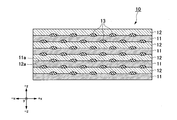
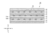
- FIG. 2 is an enlarged cross-sectional view of the domain wall motion layer 10 in the domain wall motion type magnetic recording element according to the first embodiment.
- the domain wall motion layer 10 has a first layer 11, a second layer 12, and an SOT suppression unit 13.
- the first layer 11 and the second layer 12 are alternately laminated in the z direction.
- the lowermost layer (the layer located closest to the ⁇ z direction) of the domain wall motion layer 10 in FIG. 2 is the first layer 11, but may be the second layer 12.
- the first surfaces 11a and 12a are laminated surfaces of the first layer 11 and the second layer 12.
- the first layer 11 contains a rare earth metal.
- the first layer 11 contains, for example, Tb, Gb, or an alloy thereof.
- the thickness of the first layer 11 is, for example, 0.1 to 3 nm.
- the second layer 12 contains a transition metal.
- the second layer 12 is, for example, Co, Fe, CoFeB. including.
- the thickness of the second layer 12 is, for example, 0.1 to 3 nm.
- the combination of the first layer 11 and the second layer 12 is, for example, a Gd—Co based material or a Tb—Co based material.
- Ferrimagnetic materials such as Gd—Co based materials and Tb—Co based materials have a small saturation magnetization and a small threshold current required to move the domain wall.
- the SOT suppression unit 13 is located at the interface between the first layer 11 and the second layer 12.
- the SOT suppressing part 13 contains a nonmagnetic metal.
- the SOT suppressing part 13 contains, for example, a nonmagnetic transition metal having an atomic number of 48 or less.
- the SOT suppressing unit 13 is locally distributed at the interface between the first layer 11 and the second layer 12. “Locally distributed” means that it does not exist uniformly at the interface between the first layer 11 and the second layer 12.
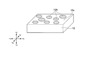
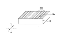
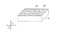
- 3 to 5 are perspective views schematically showing the distribution of the SOT suppressing units 13A to 13C.
- 3 to 5 are diagrams showing examples of distribution of the SOT suppressing portions 13A to 13C on the first surface 12a of the second layer 12.
- the SOT suppressing portions 13A to 13C in FIGS. 3 to 5 are not uniform layers, and none of them are uniformly present at the interface between the first layer 11 and the second layer 12.
- the SOT suppressing portions 13A shown in FIG. 3 are scattered on the first surface 12a of the second layer 12 in an island shape.
- the plurality of SOT suppression units 13A are discontinuously distributed.
- the SOT suppressing portions 13B shown in FIG. 4 are distributed in a strip shape on the first surface 12a of the second layer 12.
- a plurality of SOT suppressing parts 13B are discontinuously distributed.
- the SOT suppressing portion 13B extends in a direction intersecting the x direction (for example, the y direction).
- the SOT suppressing portion 13C shown in FIG. 5 has an opening through which the first surface 12a of the second layer 12 is exposed and is continuously distributed.
- the SOT suppressing portion 13A shown in FIG. 3 When the SOT suppressing portion 13A shown in FIG. 3 is sputtered under the condition that no layer is formed, the atoms are aggregated and formed.
- the condition for not forming a layer is, for example, a condition that the film formation thickness is one atomic layer or less.
- the SOT suppressing portions 13B and 13C shown in FIGS. 4 and 5 are obtained by forming a film through a mask or the like.
- the SOT suppressing portion 13 is formed by sputtering or the like as described above.
- the SOT suppressing portion 13 projects in the + z direction from, for example, an interface (first surface 11a, 12a) between the first layer 11 and the second layer 12.
- the SOT suppressing portion 13 may be recessed in the ⁇ z direction from the interfaces (first surfaces 11a and 12a) between the first layer 11 and the second layer 12.
- the total area of one interface of the SOT suppressing unit 13 is preferably 20% or more, and more preferably 30% or more of the area of the interface between the first layer 11 and the second layer 12, for example.
- the total area of one interface of the SOT suppressing portion 13 is preferably 80% or less of the area of the interface between the first layer 11 and the second layer 12, and more preferably 70% or less.
- the total area is the total area occupied by the SOT suppressing portion 13 at one interface in a plan view from the z direction.
- the SOT suppressing unit 13 prevents mixing of the rare earth metal contained in the first layer 11 and the transition metal contained in the second layer 12.
- the first layer 11 and the second layer 12 are stacked by sputtering, for example.
- the material of the second layer 12 may be mixed with the first layer 11 in some cases.
- the mixed portion causes scattering of electrons moving in the x direction in the domain wall motion layer 10.
- Electron scattering is one of the causes of the spin Hall effect.
- the spin Hall effect is a phenomenon in which a spin current is induced in a direction orthogonal to the direction of the current based on the spin-orbit interaction when a current is passed.
- the spin Hall effect develops a spin orbit torque (SOT) and gives SOT to the magnetizations M 10A and M 10B in the domain wall motion layer 10.
- the STT acts on the magnetizations M 10A and M 10B in 180 ° opposite directions.
- a current is passed from the second electrode 22 toward the first electrode 21. Since the electrons flow in the direction opposite to the current, the electrons move from the first electrode 21 toward the second electrode 22.
- the electrons that have passed through the first magnetic domain 10A become spins oriented in the ⁇ z direction under the influence of the magnetization M 10A .
- the spins oriented in the ⁇ z direction are injected into the second magnetic domain 10B.
- the ⁇ z-direction oriented spin injected into the second magnetic domain 10B applies a torque in the opposite direction by 180 ° to the magnetization M 10B oriented in the + z direction.
- the magnetization M 10B is fluctuating due to heat or the like.
- the torque in the opposite direction of 180 ° is applied at the timing when the magnetization M 10B slightly tilts from the + z direction, the magnetization M 10B reverses while performing a precession motion.
- the domain wall 10C moves in the + x direction.
- FIG. 6 is a cross-sectional view of the domain wall motion type magnetic recording element 100 for explaining the SOT.
- a current I flows from the second electrode 22 toward the first electrode 21.
- the first spin S1 oriented in one direction and the second spin S2 oriented in the opposite direction to the first spin S1 are respectively bent in a direction orthogonal to the current.
- the first spin S1 oriented in the + y direction is bent in the + z direction with respect to the traveling direction
- the second spin S2 oriented in the ⁇ y direction is bent in the ⁇ z direction with respect to the traveling direction.
- the spin Hall effect is basically unlikely to occur in a magnetic material. However, if the magnetic domain wall moving layer 10 has a portion where magnetic substances are mixed with each other, electrons are scattered at the portion, and the spin Hall effect occurs.
- the first spin S1 oriented in the + y direction and the second spin S2 oriented in the ⁇ y direction apply SOT acting in a direction inclined by 90 ° to the magnetization M 10B (see FIG. 1) oriented in the + z direction. ..
- the magnetization M 10B first falls quickly to 90 ° and then reverses. Due to the direction in which the torque acts, the magnetization reversal by SOT occurs faster than the magnetization reversal by STT.
- the SOT suppression unit 13 is located at the interface between the first layer 11 and the second layer 12.
- the SOT suppressing unit 13 prevents mixing of the first layer 11 and the second layer 12 and suppresses the expression of SOT.
- the SOT suppressing portion 13 is a non-magnetic transition metal, and the spin Hall effect does not occur even if the first layer 11 and the second layer 12 are mixed.
- the atoms forming the SOT suppressing portion 13 are lighter than the atoms forming the first layer 11 and the second layer 12. Atoms forming the SOT suppressing portion 13 are hard to be implanted into the first layer 11 and the second layer 12, and mixing itself hardly occurs.
- the SOT suppressing portion 13 does not form a layer and is locally distributed, and does not significantly impede the magnetic correlation between the first layer 11 and the second layer 12.
- the orientations of the magnetizations M 10A and M 10B of the domain wall motion layer 10 are improved and stable data retention becomes possible.
- the first ferromagnetic layer 40 is located between the first electrode 21 and the second electrode 22 in a plan view from the z direction (see FIG. 1).
- the first ferromagnetic layer 40 has a long axis in the x direction, for example.
- the first ferromagnetic layer 40 includes a ferromagnetic material.
- the ferromagnetic material forming the first ferromagnetic layer 40 include metals selected from the group consisting of Cr, Mn, Co, Fe and Ni, alloys containing one or more of these metals, and these metals and B.
- An alloy containing at least one element of C, C, and N can be used. Specific examples include Co-Fe, Co-Fe-B, and Ni-Fe.
- the material forming the first ferromagnetic layer 40 may be a Heusler alloy.
- Heusler alloy is a half metal and has a high spin polarizability.
- the Heusler alloy is an intermetallic compound having a chemical composition of XYZ or X 2 YZ, X is a transition metal element or a noble metal element of Co, Fe, Ni, or Cu group on the periodic table, and Y is Mn, V. , Cr or Ti group transition metal or X element species, and Z is a group III to V group typical element.
- Examples of the Heusler alloy include Co 2 FeSi, Co 2 FeGe, Co 2 FeGa, Co 2 MnSi, Co 2 Mn 1-a Fe a Al b Si 1-b , and Co 2 FeGe 1-c Ga c .
- the film thickness of the first ferromagnetic layer 40 is preferably 1.5 nm or less, and 1.0 nm or less when the easy magnetization axis of the first ferromagnetic layer 40 is in the z direction (perpendicular magnetization film). Is more preferable.
- the perpendicular magnetic anisotropy (interfacial perpendicular magnetic anisotropy) is generated in the first ferromagnetic layer 40 at the interface between the first ferromagnetic layer 40 and another layer (nonmagnetic layer 30).
- Anisotropy can be added. That is, the magnetization direction of the first ferromagnetic layer 40 can be set to the z direction.
- Non-magnetic layer 30 A known material can be used for the nonmagnetic layer 30.
- the nonmagnetic layer 30 is made of an insulator (when it is a tunnel barrier layer)
- Al 2 O 3 , SiO 2 , MgO, MgAl 2 O 4 or the like can be used as the material thereof.
- a material in which a part of Al, Si, Mg is replaced with Zn, Be, or the like can be used.
- MgO and MgAl 2 O 4 are materials that can realize a coherent tunnel, and therefore spins can be efficiently injected.
- the non-magnetic layer 30 is made of metal
- Cu, Au, Ag, or the like can be used as the material.
- the nonmagnetic layer 30 is made of a semiconductor, Si, Ge, CuInSe 2 , CuGaSe 2 , Cu (In, Ga) Se 2 or the like can be used as the material thereof.
- the first electrode 21 and the second electrode 22 face the domain wall motion layer 10. Another layer may be provided between the first electrode 21 and the second electrode 22 and the domain wall motion layer 10. The first electrode 21 and the second electrode 22 may face any surface of the domain wall motion layer 10. The first electrode 21 and the second electrode 22 are arranged apart from each other.
- the first electrode 21 and the second electrode 22 are magnetic materials, for example.
- the orientation of the magnetization of the first electrode 21 is the same direction as the first magnetic domain 10A (eg, ⁇ z direction), and the orientation of the magnetization of the second electrode 22 is the same direction as the second magnetic domain 10B (eg, + z direction). Is.
- the moving range of the domain wall 10C is limited.
- the magnetization of the first electrode 21 is oriented in the ⁇ z direction
- the magnetization of the first magnetic domain 10A immediately below the first electrode 21 is fixed in the ⁇ z direction.
- the movement of the domain wall 10C in the ⁇ x direction is restricted from the end of the first electrode 21 on the first ferromagnetic layer 40 side.
- the domain wall motion type magnetic recording element 100 according to the first embodiment has the SOT suppressing portion 13 to suppress the development of SOT in the domain wall motion layer 10.
- the SOT hinders the magnetization reversal due to the STT, which causes the movement of the domain wall 10C to be disturbed.
- the domain wall motion type magnetic recording element 100 according to the first embodiment can efficiently move the domain wall 10C and can be driven with low power consumption.
- FIG. 7 is an enlarged cross-sectional view of the domain wall motion layer 15 of the domain wall motion type magnetic recording element according to the first modification.
- the same components as those of the domain wall motion layer 10 shown in FIG. 2 are denoted by the same reference numerals and the description thereof will be omitted.
- the domain wall motion layer 15 has a first layer 11, a second layer 12, and an SOT suppressing portion 13.
- the SOT suppressing unit 13 exists only on the first surface 12a (lamination surface) of the second layer 12.
- the rare earth metal forming the first layer 11 is implanted into the first surface 12a of the second layer 12.
- the rare earth metal is heavier and larger than the transition metal forming the second layer 12.
- Heavy and large atoms are easily implanted in other layers by sputtering, and mixing is likely to occur. Also, the heavy and large atoms cause scattering of electrons, which causes the spin Hall effect to be remarkably exhibited. That is, the rare earth metal mixed in the second layer 12 is a cause of generating a larger SOT due to the spin Hall effect than the transition metal mixed in the first layer 11.
- FIG. 8 is an enlarged cross-sectional view of the domain wall motion layer 16 of the domain wall motion type magnetic recording element according to the second modification.
- the same components as those of the domain wall motion layer 10 shown in FIG. 2 are denoted by the same reference numerals and the description thereof will be omitted.
- the domain wall motion layer 16 has a first layer 11, a second layer 12, and an SOT suppression unit 13.
- the first surfaces 11a and 12a of the first layer 11 and the second layer 12 shown in FIG. 8 have irregularities reflecting the shape of the surfaces to be laminated. Concavities and convexities are formed on the laminated surface by the SOT suppressing portion 13 protruding from the first surfaces 11a and 12a.
- “reflecting” does not mean that the first surfaces 11a and 12a completely reflect the shape of the laminated surface. If the rate of change of the surface shape of the adjacent layer is within 10% in the z direction and within 10% in the xy direction, it can be said that the change is reflected.
- FIG. 9 is a sectional view of a domain wall motion type magnetic recording element 100A according to Modification 3.
- the same components as those of the domain wall motion type magnetic recording element 100 shown in FIG. 1 are designated by the same reference numerals and the description thereof will be omitted.
- the SOT suppressing portion 13 is in a position overlapping the first ferromagnetic layer 40 in a plan view from the z direction.
- the resistance value of the domain wall motion type magnetic recording element 100A changes depending on the magnetization state of the domain wall motion layer 10 at a position overlapping the first ferromagnetic layer 40 in a plan view from the z direction. In other words, when the domain wall 10C (see FIG. 1) is located at a position not overlapping the first ferromagnetic layer 40 in a plan view from the z direction, the resistance value of the domain wall motion type magnetic recording element 100A does not change.
- the location where the movement of the domain wall 10C should be controlled most is the portion of the domain wall moving layer 10 that overlaps the first ferromagnetic layer 40 in a plan view from the z direction.
- the magnetic domain wall motion type magnetic recording element 100A according to Modification 3 is provided with the SOT suppressing portion 13 at the relevant portion, and the movement of the magnetic domain wall 10C can be sufficiently controlled.
- FIG. 10 is a cross-sectional view of a domain wall motion type magnetic recording element 100B according to Modification 4.
- the same components as those of the domain wall motion type magnetic recording element 100 shown in FIG. 1 are designated by the same reference numerals and the description thereof will be omitted.
- the domain wall motion type magnetic recording element 100B has an underlayer 50 on the surface of the domain wall motion layer 10 opposite to the first surface 10a facing the first ferromagnetic layer 40.
- the underlayer 50 controls crystallinity such as crystal orientation and crystal grain size of each layer including the first ferromagnetic metal layer 1.
- the magnetization M 10A of the domain wall displacement layer 10 enhances the orientation of the magnetization M 40 of the M 10B and the first ferromagnetic layer 40, to increase the rate of change in resistance of the domain wall motion type magnetic recording element 100B.
- the underlayer 50 is a single layer of Ru, Ti, Cu, SiO 2 , MgO or SiN or a laminated body of these.
- a spin Hall effect occurs in the underlayer 50.
- Spins oriented in one direction due to the spin Hall effect move in the + z direction and are injected into the domain wall motion layer 10 (see FIG. 6).
- the spin injected into the domain wall motion layer 10 causes the movement of the domain wall 10C to be hindered.
- the underlayer 50 does not hinder the movement of the domain wall 10C.
- FIG. 11 is a perspective view of a domain wall motion type magnetic recording element 100C according to Modification 5.
- the magnetic domain wall motion type magnetic recording element 100C shown in FIG. 11 is different from the magnetic domain wall motion type magnetic recording element 100 shown in FIG. 1 in that the second ferromagnetic layer 60 is provided between the magnetic domain wall motion layer 10 and the non-magnetic layer 30. different.
- the second ferromagnetic layer 60 reflects the magnetic state of the domain wall motion layer 10.
- the second ferromagnetic layer 60 contains a magnetic material.
- the magnetic material forming the second ferromagnetic layer 60 the same magnetic material as that of the first ferromagnetic layer 40 can be used.
- the second ferromagnetic layer 60 is adjacent to the domain wall displacement layer 10.
- the magnetizations M 60A and M 60B of the second ferromagnetic layer 60 are magnetically coupled to the magnetization of the domain wall motion layer 10.
- the second ferromagnetic layer 60 reflects the magnetic state of the domain wall motion layer 10.
- the magnetic state of the second ferromagnetic layer 60 is the same as the magnetic state of the domain wall displacement layer 10.
- the magnetic state of the second ferromagnetic layer 60 is opposite to the magnetic state of the domain wall displacement layer 10.
- the MR ratio of the domain wall motion type magnetic recording element 100C is caused by a change in the magnetic state of the two magnetic bodies (the first ferromagnetic layer 40 and the second ferromagnetic layer 60) that sandwich the nonmagnetic layer 30.
- the second ferromagnetic layer 60 preferably contains a material that easily obtains the coherent tunnel effect with the first ferromagnetic layer 40.
- the domain wall moving layer 10 contains a material that makes the moving speed of the domain wall 10C slow.
- the domain wall motion layer 10 is one of the two magnetic bodies sandwiching the nonmagnetic layer 30.
- the domain wall motion layer 10 is made of a material that allows the domain wall motion speed of the domain wall 10C to be slow and improves the MR ratio of the domain wall motion type magnetic recording element 100. Is preferred.
- the domain wall motion layer 10 is not two magnetic bodies sandwiching the nonmagnetic layer 30.
- the material forming the domain wall motion layer 10 has little influence on the MR ratio of the domain wall motion type magnetic recording element 100C. Therefore, in the domain wall motion type magnetic recording element 100C shown in FIG. 11, the degree of freedom in selecting the material of the domain wall motion layer 10 is increased.
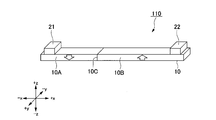
- FIG. 12 is a perspective view of the domain wall motion element 110 according to the second embodiment.
- the domain wall motion element 110 shown in FIG. 12 differs from the domain wall motion type magnetic recording element 100 shown in FIG. 1 in that it does not have the nonmagnetic layer 30 and the first ferromagnetic layer 40.
- the domain wall motion element 110 according to the second embodiment can be applied to the above domain wall motion type magnetic recording element. Further, the present invention is not limited to this application, but can be applied to other applications. As another application, for example, the domain wall motion element 110 can be provided in each pixel and used as a spatial light modulator that spatially modulates incident light by utilizing a magneto-optical effect.
- FIG. 13 is a plan view of the magnetic recording array 120 according to the third embodiment.
- the domain wall motion type magnetic recording element 100 shown in FIG. 1 is arranged in a 3 ⁇ 3 matrix.
- FIG. 13 shows an example of the magnetic recording array, and the type, number and arrangement of the domain wall motion type magnetic recording elements 100 are arbitrary. Further, instead of the domain wall motion type magnetic recording element 100 shown in FIG. 1, a domain wall motion type magnetic recording element according to a modified example may be used.
- One word line WL1 to WL3, one bit line BL1 to BL3, and one read line RL1 to RL3 are connected to each domain wall motion type magnetic recording element 100.
- a pulse current is passed through the domain wall motion layer 10 of any domain wall motion type magnetic recording element 100 to perform a write operation. Further, by selecting the read lines RL1 to RL3 and the bit lines BL1 to BL3 to which a current is applied, a current is caused to flow in the stacking direction of the domain wall motion type magnetic recording element 100, and a reading operation is performed.
- the word lines WL1 to WL3, the bit lines BL1 to BL3, and the read lines RL1 to RL3 to which current is applied can be selected by transistors or the like.
- the domain wall motion type magnetic recording element 100 can record data in analog instead of digital signals of "1" and "0". Therefore, the magnetic recording array 120 can be used in a neuromorphic device that imitates the brain.
Landscapes
- Engineering & Computer Science (AREA)
- Chemical & Material Sciences (AREA)
- Crystallography & Structural Chemistry (AREA)
- Power Engineering (AREA)
- Computer Hardware Design (AREA)
- Hall/Mr Elements (AREA)
- Mram Or Spin Memory Techniques (AREA)
- Thin Magnetic Films (AREA)
Abstract
この磁壁移動型磁気記録素子(100)は、希土類金属を含む第1層(11)と遷移金属を含む第2層(12)とが、第1方向(Z)に向かって交互に積層された磁壁移動層(10)と、前記磁壁移動層に面し、互いに離間して配置された第1電極(21)及び第2電極(22)と、を備え、前記磁壁移動層は、前記第1層と前記第2層とのいずれかの界面に位置し、非磁性の金属を含むSOT抑制部(13)を有し、前記SOT抑制部は、前記界面において局所的に分布する。
Description
本発明は、磁壁移動素子、磁壁移動型磁気記録素子及び磁気記録アレイに関する。
微細化に限界が見えてきたフラッシュメモリ等に代わる次世代の不揮発性メモリとして、抵抗変化型素子を利用してデータを記憶する抵抗変化型の磁気記録装置に注目が集まっている。磁気記録装置の一例としては、MRAM(Magnetoresistive Random Access Memory)、ReRAM(Resistance Randome Access Memory)、PCRAM(Phase Change Random Access Memory)等がある。
MRAMは、磁化の向きによって生じる抵抗値変化をデータ記録に利用している。記録メモリの大容量化を実現するために、メモリを構成する素子の小型化、メモリを構成する素子一つあたりの記録ビットの多値化が検討されている。
特許文献1には、磁気記録層内における磁壁を移動させることで、多値のデータを記録することができる磁壁移動型磁気記録素子が記載されている。
磁壁移動型磁気記録素子は、低消費電力化が求められている。磁壁移動型磁気記録素子は、磁壁の位置を制御することで、データを記録する。磁壁移動型磁気記録素子の低消費電力化を実現する一つの方法は、磁壁を移動させるのに必要なエネルギーを小さくすることである。磁壁を効率的に動かすことができる磁壁移動型磁気記録素子が求められている。
本発明は上記問題に鑑みてなされたものであり、低消費電力な磁壁移動素子、磁壁移動型磁気記録素子及び磁気記録アレイを提供することを目的とする。
(1)第1の態様にかかる磁壁移動素子は、希土類金属を含む第1層と遷移金属を含む第2層とが、第1方向に向かって交互に積層された磁壁移動層と、前記磁壁移動層に面し、互いに離間して配置された第1電極及び第2電極と、を備え、前記磁壁移動層は、前記第1層と前記第2層とのいずれかの界面に位置し、非磁性の金属を含むSOT抑制部を有し、前記SOT抑制部は、前記界面において局所的に分布する。
(2)上記態様にかかる磁壁移動素子において、前記SOT抑制部は、原子番号48以下の非磁性遷移金属を含んでもよい。
(3)上記態様にかかる磁壁移動素子において、前記SOT抑制部は、前記界面において不連続に分布してもよい。
(4)上記態様にかかる磁壁移動素子において、前記SOT抑制部は、前記界面において島状に点在してもよい。
(5)上記態様にかかる磁壁移動素子において、前記SOT抑制部は、前記界面から前記第1方向に向かって突出してもよい。
(6)上記態様にかかる磁壁移動素子において、前記SOT抑制部は、前記第2層の積層面上にあってもよい。
(7)上記態様にかかる磁壁移動素子において、前記SOT抑制部は、前記第2層の積層面上のみにあってもよい。
(8)上記態様にかかる磁壁素子において、前記SOT抑制部の一つの界面における総面積は、前記界面の面積の20%以上であってもよい。
(9)上記態様にかかる磁壁移動型磁気記録素子において、前記第1層は、Tb、Gb、又は、これらの合金を含んでもよい。
(10)第2の態様にかかる磁壁移動型磁気記録素子は、上記態様にかかる磁壁移動素子と、前記磁壁移動層に面し、前記第1方向からの平面視で前記第1電極と前記第2電極との間に位置する第1強磁性層と、前記第1強磁性層と前記磁壁移動層との間に位置する非磁性層と、を備える。
(11)上記態様にかかる磁壁移動型磁気記録素子において、前記SOT抑制部は、前記第1方向からの平面視で、前記第1強磁性層と重なる位置にあってもよい。
(12)上記態様にかかる磁壁移動型磁気記録素子において、前記磁壁移動層と前記非磁性層との間に、前記第2強磁性層をさらに備えてもよい。
(13)上記態様にかかる磁壁移動型磁気記録素子において、前記磁壁移動層の前記第1強磁性層に面する第1面と反対側の面に、下地層をさらに備え、前記下地層は、Ru、Ti、Cu、SiO2、MgO又はSiNの単層又はこれらの積層体であってもよい。
(14)第3の態様にかかる磁気記録アレイは、上記態様にかかる磁壁移動型磁気記録素子を複数備える。
上記態様にかかる磁壁移動素子、磁壁移動型磁気記録素子及び磁気記録アレイは、少ない消費電力で動作する。
以下、本実施形態について、図を適宜参照しながら詳細に説明する。以下の説明で用いる図面は、本発明の特徴をわかりやすくするために便宜上特徴となる部分を拡大して示している場合があり、各構成要素の寸法比率などは実際とは異なっていることがある。以下の説明において例示される材料、寸法等は一例であって、本発明はそれらに限定されるものではなく、本発明の効果を奏する範囲で適宜変更して実施することが可能である。
方向について定義する。+z方向は、後述する磁壁移動層10を支持する支持体(図示略)に対して積層する方向である。-z方向は、その反対方向である。+z方向と-z方向とを区別しない場合は、単に「z方向」という。+x方向は、z方向と略直交し、後述する第1電極21から第2電極22へ向かう方向である。-x方向はその反対方向である。+x方向と-x方向とを区別しない場合は、単に「x方向」という。+y方向は、z方向及びx方向と直交する一方向である。-y方向は、その反対の方向である。+y方向と-y方向とを区別しない場合は、単に「y方向」という。第1方向は、+z方向の一例である。
(磁壁移動型磁気記録素子)
「第1実施形態」
図1は、第1実施形態にかかる磁壁移動型磁気記録素子100を模式的に示した斜視図である。磁壁移動型磁気記録素子100は、磁壁移動層10と2つの電極20と非磁性層30と第1強磁性層40とを備える。2つの電極20の一方が第1電極21であり、他方が第2電極22である。磁壁移動層10は、第1磁区10Aと第2磁区10Bとを有し、これらの境界に磁壁10Cを有する。
「第1実施形態」
図1は、第1実施形態にかかる磁壁移動型磁気記録素子100を模式的に示した斜視図である。磁壁移動型磁気記録素子100は、磁壁移動層10と2つの電極20と非磁性層30と第1強磁性層40とを備える。2つの電極20の一方が第1電極21であり、他方が第2電極22である。磁壁移動層10は、第1磁区10Aと第2磁区10Bとを有し、これらの境界に磁壁10Cを有する。
磁壁移動型磁気記録素子100は、磁壁移動層10の磁壁10Cの位置によって、データを多値で記録する。磁壁移動型磁気記録素子100は、第1強磁性層40、非磁性層30及び磁壁移動層10の積層方向の抵抗値としてデータを記録する。磁壁移動型磁気記録素子100の抵抗値は、z方向から見て第1強磁性層40と重なる位置における磁壁移動層10の磁化M10A、M10Bの状態により変化する。
第1磁区10Aの磁化M10Aの向きは、第1強磁性層40の磁化M40の向きと反対方向(反平行)である。第2磁区10Bの磁化M10Bの向きは、第1強磁性層40の磁化M40の向きと同方向(平行)である。z方向から見て第1強磁性層40と重畳する部分における第1磁区10Aの面積が広くなると、磁壁移動型磁気記録素子100の抵抗値は高くなる。z方向から見て第1強磁性層40と重畳する部分における第2磁区10Bの面積が広くなると、磁壁移動型磁気記録素子100の抵抗値は低くなる。つまり、磁壁移動型磁気記録素子100の抵抗値は、磁壁10Cが+x方向に移動すると高くなり、-x方向に移動すると低くなる。
磁壁移動型磁気記録素子100にデータを書き込む際は、例えば、第1電極21と第2電極22との間に書き込み電流を流す。例えば、磁壁移動層10に所定の方向の電流パルスを印加すると、第1磁区10Aは第2磁区10Bへ広がり、磁壁10Cが第2電極22へ向かって移動する。磁壁移動型磁気記録素子100の抵抗値は、磁壁10Cの位置で決まり、データが書き込まれる。磁壁10Cの位置は、磁壁移動層10に流す電流の方向(+x方向又は-x方向)、電流密度等により制御できる。また磁壁10Cの位置は、磁壁移動層10に外部磁場を印加することでも制御できる。
磁壁移動型磁気記録素子100からデータを読み出す際は、第1強磁性層40と、第1電極21又は第2電極22との間に読み出し電流を流す。読み出し電流は、書き込み電流より小さく、磁壁10Cは移動しない。磁壁移動型磁気記録素子100の抵抗値は、磁壁移動層10及び第1強磁性層40に対してz方向に読み出し電流を印加することで、オームの法則から求められる。磁壁移動型磁気記録素子100の抵抗値は、データに変換される。
<磁壁移動層>
図2は、第1実施形態にかかる磁壁移動型磁気記録素子における磁壁移動層10を拡大した断面図である。磁壁移動層10は、第1層11と第2層12とSOT抑制部13とを有する。
図2は、第1実施形態にかかる磁壁移動型磁気記録素子における磁壁移動層10を拡大した断面図である。磁壁移動層10は、第1層11と第2層12とSOT抑制部13とを有する。
第1層11と第2層12とは、z方向に交互に積層されている。図2における磁壁移動層10の最下層(最も-z方向に位置する層)は、第1層11であるが、第2層12でもよい。第1面11a、12aは、第1層11及び第2層12の積層面である。
第1層11は、希土類金属を含む。第1層11は、例えば、Tb、Gb、又は、これらの合金を含む。第1層11の厚みは、例えば、0.1~3nmである。
第2層12は、遷移金属を含む。第2層12は、例えば、Co、Fe、CoFeBである。を含む。第2層12の厚みは、例えば、0.1~3nmである。
第1層11及び第2層12の組み合わせは、例えば、Gd-Co系材料、Tb-Co系材料である。Gd-Co系材料、Tb-Co系材料等のフェリ磁性体は、飽和磁化が小さく、磁壁を移動するために必要な閾値電流が小さい。
SOT抑制部13は、第1層11と第2層12との界面に位置する。SOT抑制部13は、非磁性の金属を含む。SOT抑制部13は、例えば、原子番号48以下の非磁性遷移金属を含む。
SOT抑制部13は、第1層11と第2層12との界面において、局所的に分布する。「局所的に分布する」とは、第1層11と第2層12との界面において一様に存在しないことを意味する。
図3から図5は、SOT抑制部13A~13Cの分布を模式的に示した斜視図である。図3から図5は、第2層12の第1面12aにおけるSOT抑制部13A~13Cの分布の例を示した図である。図3から図5におけるSOT抑制部13A~13Cは均一な層となっておらず、いずれも第1層11と第2層12との界面において一様に存在しない。
図3に示すSOT抑制部13Aは、第2層12の第1面12aに島状に点在している。複数のSOT抑制部13Aは、不連続に分布している。
図4に示すSOT抑制部13Bは、第2層12の第1面12aに帯状に分布している。複数のSOT抑制部13Bが不連続に分布している。SOT抑制部13Bは、x方向と交差する方向(例えば、y方向)に延びる。
図5に示すSOT抑制部13Cは、第2層12の第1面12aが露出する開口部を有し、連続して分布している。
図3に示すSOT抑制部13Aは、層を形成しない条件でスパッタリングを行うと、原子同士が凝集し形成される。層を形成しない条件は、例えば、成膜厚みが一原子層以下の厚みとなる条件である。図4及び図5に示すSOT抑制部13B,13Cは、マスク等を介して成膜することで得られる。
図3から図5は、第2層12の第1面12aを例に説明したが、第1層11の第1面11aも同様である。また複数の第1層11及び第2層12のそれぞれの第1面11a、12aにおけるSOT抑制部13の分布は同一である必要はなく、それぞれ異なっていてもよい。
SOT抑制部13は、上述のようにスパッタリング等により形成される。SOT抑制部13は、例えば、第1層11と第2層12との界面(第1面11a、12a)から+z方向に突出する。スパッタリング時の打ち込み強度によっては、SOT抑制部13は、第1層11と第2層12との界面(第1面11a、12a)から-z方向に窪んでもよい。
SOT抑制部13の一つの界面における総面積は、例えば、第1層11と第2層12との界面の面積の20%以上であることが好ましく、30%以上であることがより好ましい。またSOT抑制部13の一つの界面における総面積は、例えば、第1層11と第2層12との界面の面積の80%以下であることが好ましく、70%以下であることがより好ましい。総面積は、z方向からの平面視で、一つの界面においてSOT抑制部13が占める全面積である。
SOT抑制部13は、第1層11に含まれる希土類金属と、第2層12に含まれる遷移金属と、のミキシングを防ぐ。第1層11及び第2層12は、例えば、スパッタリングで積層される。例えば、第1層11の第1面11aに第2層12を構成する元素を打ち込むと、第1層11に第2層12の材料がミキシングする場合がある。
ミキシングが生じた部分は、磁壁移動層10内をx方向に移動する電子の散乱原因となる。電子の散乱は、スピンホール効果を生み出す原因の一つである。スピンホール効果は、電流を流した場合にスピン軌道相互作用に基づき、電流の向きと直交する方向にスピン流が誘起される現象である。スピンホール効果は、スピン軌道トルク(SOT)を発現し、磁壁移動層10内の磁化M10A、M10BにSOTを与える。
ここで磁壁移動層10内の磁化M10A、M10Bの反転に作用するスピントランスファートルク(STT)とSOTについて説明する。
STTは、磁化M10A、M10Bに対して180°反対方向に作用する。例えば、図1において第2電極22から第1電極21に向って電流を流す。電子は電流と反対方向に流れるため、電子は第1電極21から第2電極22に向かって移動する。第1磁区10Aを通過した電子は、磁化M10Aの影響を受けて-z方向に配向したスピンとなる。-z方向に配向したスピンは、第2磁区10Bに注入される。第2磁区10Bに注入された-z方向に配向したスピンは、+z方向に配向した磁化M10Bに対して180°反対方向のトルクを加える。磁化M10Bは、熱等で揺らいでいる。磁化M10Bが+z方向からわずかに傾いたタイミングで、180°反対方向のトルクが加わると、磁化M10Bは歳差運動をしながら反転する。第2磁区10Bの磁化M10Bの一部が反転すると、磁壁10Cは+x方向に移動する。
これに対しSOTは、磁化M10A、M10Bに対して90°傾いた方向に作用する。図6は、SOTについて説明するための磁壁移動型磁気記録素子100の断面図である。例えば、図6に示すように第2電極22から第1電極21に向って電流Iを流す。スピンホール効果が生じると、一方向に配向した第1スピンS1と、第1スピンS1と反対方向に配向した第2スピンS2とは、それぞれ電流と直交する方向に曲げられる。例えば、+y方向に配向した第1スピンS1は進行方向に対し+z方向に曲げられ、-y方向に配向した第2スピンS2は進行方向に対して-z方向に曲げられる。
スピンホール効果は、磁性体中では基本的に生じにくい。しかしながら、磁壁移動層10に磁性体同士がミキシングした部分があると、その部分で電子が散乱し、スピンホール効果が生じる。+y方向に配向した第1スピンS1及び-y方向に配向した第2スピンS2は、+z方向に配向した磁化M10B(図1参照)に対して、90°傾いた方向に作用するSOTを加える。磁化M10Bは、まず90°まで素早く倒れ、その後反転する。トルクの作用する方向の関係上、SOTによる磁化反転は、STTによる磁化反転より素早く生じる。
磁壁移動層10の磁化M10A、M10Bに対してSTTとSOTとが同時に作用すると、STTとSOTとは作用するベクトル方向が異なるため、SOTはSTTによる磁化M10A、M10Bの歳差運動を乱す。すなわち、SOTは、STTによる磁化M10A、M10Bの反転を乱す原因となる。換言すると、SOTの発現を抑制できると、磁壁移動層10の磁壁10Cの移動が効率的になる。
SOT抑制部13は、第1層11と第2層12との界面に位置する。SOT抑制部13は、第1層11と第2層12とのミキシングを防ぎ、SOTの発現を抑制する。SOT抑制部13は、非磁性の遷移金属であり、第1層11と第2層12とミキシングが生じても、スピンホール効果は生じない。またSOT抑制部13を構成する原子は、第1層11及び第2層12を構成する原子より軽い。SOT抑制部13を構成する原子は、第1層11及び第2層12に打ち込まれにくく、ミキシング自体がほとんど生じない。
またSOT抑制部13は、層を形成しておらず、局所的に分布しており、第1層11と第2層12との磁気的な相関を大きく阻害しない。第1層11と第2層12との磁気的な相関が維持されることで、磁壁移動層10の磁化M10A、M10Bの配向性が向上し、データの安定した保持が可能となる。
<第1強磁性層>
第1強磁性層40は、z方向から平面視で第1電極21と第2電極22との間に位置する(図1参照)。第1強磁性層40は、例えばx方向に長軸を有する。
第1強磁性層40は、z方向から平面視で第1電極21と第2電極22との間に位置する(図1参照)。第1強磁性層40は、例えばx方向に長軸を有する。
第1強磁性層40は、強磁性体を含む。第1強磁性層40を構成する強磁性材料としては、例えば、Cr、Mn、Co、Fe及びNiからなる群から選択される金属、これらの金属を1種以上含む合金、これらの金属とB、C、及びNの少なくとも1種以上の元素とが含まれる合金等を用いることができる。具体的には、Co-Fe、Co-Fe-B、Ni-Feが挙げられる。
また第1強磁性層40を構成する材料は、ホイスラー合金でもよい。ホイスラー合金はハーフメタルであり、高いスピン分極率を有する。ホイスラー合金は、XYZまたはX2YZの化学組成をもつ金属間化合物であり、Xは周期表上でCo、Fe、Ni、あるいはCu族の遷移金属元素または貴金属元素であり、YはMn、V、CrあるいはTi族の遷移金属又はXの元素種であり、ZはIII族からV族の典型元素である。ホイスラー合金として例えば、Co2FeSi、Co2FeGe、Co2FeGa、Co2MnSi、Co2Mn1-aFeaAlbSi1-b、Co2FeGe1-cGac等が挙げられる。
第1強磁性層40の膜厚は、第1強磁性層40の磁化容易軸をz方向とする(垂直磁化膜にする)場合は、1.5nm以下とすることが好ましく、1.0nm以下とすることがより好ましい。第1強磁性層40の膜厚を薄くすると、第1強磁性層40と他の層(非磁性層30)との界面で、第1強磁性層40に垂直磁気異方性(界面垂直磁気異方性)を付加できる。すなわち、第1強磁性層40の磁化の向きをz方向にできる。
<非磁性層>
非磁性層30には、公知の材料を用いることができる。
例えば、非磁性層30が絶縁体からなる場合(トンネルバリア層である場合)、その材料としては、Al2O3、SiO2、MgO、及び、MgAl2O4等を用いることができる。また、これらの他にも、Al、Si、Mgの一部が、Zn、Be等に置換された材料等も用いることができる。これらの中でも、MgOやMgAl2O4はコヒーレントトンネルが実現できる材料であるため、スピンを効率よく注入できる。非磁性層30が金属からなる場合、その材料としては、Cu、Au、Ag等を用いることができる。さらに、非磁性層30が半導体からなる場合、その材料としては、Si、Ge、CuInSe2、CuGaSe2、Cu(In,Ga)Se2等を用いることができる。
非磁性層30には、公知の材料を用いることができる。
例えば、非磁性層30が絶縁体からなる場合(トンネルバリア層である場合)、その材料としては、Al2O3、SiO2、MgO、及び、MgAl2O4等を用いることができる。また、これらの他にも、Al、Si、Mgの一部が、Zn、Be等に置換された材料等も用いることができる。これらの中でも、MgOやMgAl2O4はコヒーレントトンネルが実現できる材料であるため、スピンを効率よく注入できる。非磁性層30が金属からなる場合、その材料としては、Cu、Au、Ag等を用いることができる。さらに、非磁性層30が半導体からなる場合、その材料としては、Si、Ge、CuInSe2、CuGaSe2、Cu(In,Ga)Se2等を用いることができる。
<第1電極、第2電極>
第1電極21及び第2電極22は、磁壁移動層10に面する。第1電極21及び第2電極22と磁壁移動層10との間に、他の層を有してもよい。第1電極21及び第2電極22は、磁壁移動層10のいずれの面に面してもよい。第1電極21及び第2電極22は、互いに離間して配置される。
第1電極21及び第2電極22は、磁壁移動層10に面する。第1電極21及び第2電極22と磁壁移動層10との間に、他の層を有してもよい。第1電極21及び第2電極22は、磁壁移動層10のいずれの面に面してもよい。第1電極21及び第2電極22は、互いに離間して配置される。
第1電極21及び第2電極22は、例えば、磁性体である。第1電極21の磁化の配向方向は第1磁区10Aと同じ方向(例えば、-z方向)であり、第2電極22の磁化の配向方向は第2磁区10Bと同じ方向(例えば、+z方向)である。第1電極21及び第2電極22の磁化が所定の方向に固定されていると、磁壁10Cの移動範囲が限定される。例えば、第1電極21の磁化が-z方向に配向していると、第1電極21の直下の第1磁区10Aの磁化は-z方向に固定される。磁壁10Cは、第1電極21の第1強磁性層40側の端部より-x方向への移動が制限される。
第1実施形態にかかる磁壁移動型磁気記録素子100は、SOT抑制部13を有することで、磁壁移動層10内にSOTが発現することが抑制されている。SOTは、STTによる磁化反転を阻害するため、磁壁10Cの移動を乱す原因となる。第1実施形態にかかる磁壁移動型磁気記録素子100は、磁壁10Cを効率的に動かすことができ、少ない消費電力で駆動できる。
以上、第1実施形態にかかる磁壁移動型磁気記録素子100の一例について詳述したが、本発明の趣旨から逸脱しない範囲内で、構成の付加、省略、置換、及びその他の変更が可能である。
「変形例1」
図7は、変形例1にかかる磁壁移動型磁気記録素子の磁壁移動層15を拡大した断面図である。図2に示す磁壁移動層10と同一の構成については、同様の符号を付し、説明を省く。磁壁移動層15は、第1層11と第2層12とSOT抑制部13とを有する。
図7は、変形例1にかかる磁壁移動型磁気記録素子の磁壁移動層15を拡大した断面図である。図2に示す磁壁移動層10と同一の構成については、同様の符号を付し、説明を省く。磁壁移動層15は、第1層11と第2層12とSOT抑制部13とを有する。
変形例1において、SOT抑制部13は、第2層12の第1面12a(積層面)上にのみ存在する。第2層12の第1面12aは、第1層11を構成する希土類金属が打ち込まれる。希土類金属は、第2層12を構成する遷移金属より重く大きい。重く大きい原子は、スパッタリングにより他の層に打ち込まれやすく、ミキシングを生じやすい。また重く大きい原子は、電子の散乱原因となり、スピンホール効果を顕著に発現する原因となる。つまり、第1層11にミキシングした遷移金属よりも第2層12にミキシングした希土類金属の方が、スピンホール効果による大きなSOTを生じさせる原因となる。第2層12の第1面12aをSOT抑制部13で保護することで、SOTの発現を抑制できる。
「変形例2」
図8は、変形例2にかかる磁壁移動型磁気記録素子の磁壁移動層16を拡大した断面図である。図2に示す磁壁移動層10と同一の構成については、同様の符号を付し、説明を省く。磁壁移動層16は、第1層11と第2層12とSOT抑制部13とを有する。
図8は、変形例2にかかる磁壁移動型磁気記録素子の磁壁移動層16を拡大した断面図である。図2に示す磁壁移動層10と同一の構成については、同様の符号を付し、説明を省く。磁壁移動層16は、第1層11と第2層12とSOT抑制部13とを有する。
図8に示す第1層11及び第2層12の第1面11a、12aは、積層される面の形状を反映し、凹凸を有する。第1面11a、12aから突出したSOT抑制部13により積層面に凹凸が形成される。ここで「反映」とは、第1面11a、12aが、積層される積層面の形状を完全に反映させることまでは要しない。隣接する層の表面形状の変化率が、z方向に対して10%以内、かつ、xy方向に対して10%以内であれば、反映していると言える。
「変形例3」
図9は、変形例3にかかる磁壁移動型磁気記録素子100Aの断面図である。図1に示す磁壁移動型磁気記録素子100と同一の構成については、同様の符号を付し、説明を省く。
図9は、変形例3にかかる磁壁移動型磁気記録素子100Aの断面図である。図1に示す磁壁移動型磁気記録素子100と同一の構成については、同様の符号を付し、説明を省く。
磁壁移動型磁気記録素子100Aは、SOT抑制部13がz方向からの平面視で、第1強磁性層40と重なる位置にある。磁壁移動型磁気記録素子100Aの抵抗値は、z方向からの平面視で第1強磁性層40と重なる位置における磁壁移動層10の磁化の状態によって変化する。換言すると、z方向からの平面視で第1強磁性層40と重ならない位置に磁壁10C(図1参照)が位置する場合は、磁壁移動型磁気記録素子100Aの抵抗値は変化しない。従って、磁壁10Cの動きを最も制御すべき箇所は、磁壁移動層10においてz方向からの平面視で第1強磁性層40と重なる部分である。変形例3にかかる磁壁移動型磁気記録素子100Aは、当該部分にSOT抑制部13が設けられており、磁壁10Cの移動を十分制御できる。
「変形例4」
図10は、変形例4にかかる磁壁移動型磁気記録素子100Bの断面図である。図1に示す磁壁移動型磁気記録素子100と同一の構成については、同様の符号を付し、説明を省く。
図10は、変形例4にかかる磁壁移動型磁気記録素子100Bの断面図である。図1に示す磁壁移動型磁気記録素子100と同一の構成については、同様の符号を付し、説明を省く。
磁壁移動型磁気記録素子100Bは、磁壁移動層10の第1強磁性層40に面する第1面10aと反対側の面に、下地層50を有する。
下地層50は、第1強磁性金属層1を含む各層の結晶配向性、結晶粒径等の結晶性を制御する。下地層50は、磁壁移動層10の磁化M10A、M10B及び第1強磁性層40の磁化M40の配向性を高め、磁壁移動型磁気記録素子100Bの抵抗変化率を大きくする。
下地層50は、Ru、Ti、Cu、SiO2、MgO又はSiNの単層又はこれらの積層体である。下地層50に電流が流れると、下地層50でスピンホール効果が生じる。スピンホール効果により一方向に配向したスピン(例えば、+y方向)は、+z方向に移動し、磁壁移動層10に注入される(図6参照)。磁壁移動層10に注入されたスピンは、磁壁10Cの移動を阻害する原因となる。上記の材料が下地層50に用いられると、下地層50に電流がほとんど流れない、または、流れてもスピンホール効果が生じにくい。すなわち、下地層50が磁壁10Cの移動を阻害しない。
「変形例5」
図11は、変形例5にかかる磁壁移動型磁気記録素子100Cの斜視図である。図11に示す磁壁移動型磁気記録素子100Cは、磁壁移動層10と非磁性層30との間に、第2強磁性層60を備える点が、図1に示す磁壁移動型磁気記録素子100と異なる。第2強磁性層60は、磁壁移動層10の磁気状態を反映する。
図11は、変形例5にかかる磁壁移動型磁気記録素子100Cの斜視図である。図11に示す磁壁移動型磁気記録素子100Cは、磁壁移動層10と非磁性層30との間に、第2強磁性層60を備える点が、図1に示す磁壁移動型磁気記録素子100と異なる。第2強磁性層60は、磁壁移動層10の磁気状態を反映する。
第2強磁性層60は、磁性体を含む。第2強磁性層60を構成する磁性体は、第1強磁性層40と同様のものを用いることができる。
第2強磁性層60は、磁壁移動層10と互いに隣り合う。第2強磁性層60の磁化M60A、M60Bは、磁壁移動層10の磁化と磁気結合している。第2強磁性層60は、磁壁移動層10の磁気状態を反映する。第2強磁性層60と磁壁移動層10とが強磁性カップリングする場合は、第2強磁性層60の磁気状態は磁壁移動層10の磁気状態と同一になる。第2強磁性層60と磁壁移動層10とが反強磁性カップリングする場合は、第2強磁性層60の磁気状態は磁壁移動層10の磁気状態と反対になる。
磁壁移動型磁気記録素子100CのMR比は、非磁性層30を挟む2つの磁性体(第1強磁性層40と第2強磁性層60)の磁気状態の変化により生じる。第2強磁性層60は、第1強磁性層40との間で、コヒーレントトンネル効果を得やすい材料を含むことが好ましい。
一方で、磁壁移動層10は、磁壁10Cの移動速度が遅くなる材料を含むことが好ましい。図1に示す磁壁移動型磁気記録素子100の場合、磁壁移動層10は、非磁性層30を挟む2つの磁性体の一方である。図1に示す磁壁移動型磁気記録素子100の場合、磁壁移動層10は、磁壁10Cの移動速度が遅く、かつ、磁壁移動型磁気記録素子100のMR比を向上できる材料により構成されていることが好ましい。これに対し、図11に示す磁壁移動型磁気記録素子100Cの場合、磁壁移動層10は、非磁性層30を挟む2つの磁性体ではない。図11に示す磁壁移動型磁気記録素子100Cの場合、磁壁移動層10を構成する材料は、磁壁移動型磁気記録素子100CのMR比への影響が少ない。したがって、図11に示す磁壁移動型磁気記録素子100Cは、磁壁移動層10の材料選択の自由度が高まる。
「第2実施形態」
図12は、第2実施形態にかかる磁壁移動素子110の斜視図である。図12に示す磁壁移動素子110は、非磁性層30及び第1強磁性層40を有さない点が、図1に示す磁壁移動型磁気記録素子100と異なる。
図12は、第2実施形態にかかる磁壁移動素子110の斜視図である。図12に示す磁壁移動素子110は、非磁性層30及び第1強磁性層40を有さない点が、図1に示す磁壁移動型磁気記録素子100と異なる。
第2実施形態にかかる磁壁移動素子110は、上述の磁壁移動型磁気記録素子に適用することができる。またこの用途に限られず、他の用途にも適用できる。他の用途としては、例えば、磁壁移動素子110を各画素に配設して、磁気光学効果を利用して入射光を空間的に変調する空間光変調器に用いることができる。
「第3実施形態」
図13は、第3実施形態にかかる磁気記録アレイ120の平面図である。図13に示す磁気記録アレイ120は、図1に示す磁壁移動型磁気記録素子100が3×3のマトリックス配置をしている。図13は、磁気記録アレイの一例であり、磁壁移動型磁気記録素子100の種類、数及び配置は任意である。また図1に示す磁壁移動型磁気記録素子100に代えて、変形例にかかる磁壁移動型磁気記録素子を用いてもよい。
図13は、第3実施形態にかかる磁気記録アレイ120の平面図である。図13に示す磁気記録アレイ120は、図1に示す磁壁移動型磁気記録素子100が3×3のマトリックス配置をしている。図13は、磁気記録アレイの一例であり、磁壁移動型磁気記録素子100の種類、数及び配置は任意である。また図1に示す磁壁移動型磁気記録素子100に代えて、変形例にかかる磁壁移動型磁気記録素子を用いてもよい。
それぞれの磁壁移動型磁気記録素子100には、それぞれ1本のワードラインWL1~WL3と、1本のビットラインBL1~BL3、1本のリードラインRL1~RL3が接続されている。
電流を印加するワードラインWL1~WL3及びビットラインBL1~BL3を選択することで、任意の磁壁移動型磁気記録素子100の磁壁移動層10にパルス電流を流し、書き込み動作を行う。また電流を印加するリードラインRL1~RL3及びビットラインBL1~BL3を選択することで、任意の磁壁移動型磁気記録素子100の積層方向に電流を流し、読み込み動作を行う。電流を印加するワードラインWL1~WL3、ビットラインBL1~BL3、及びリードラインRL1~RL3はトランジスタ等により選択できる。それぞれが多値で情報を記録できる複数の磁壁移動型磁気記録素子100にデータを記録することで、磁気記録アレイ120の高容量化を実現できる。
また磁壁移動型磁気記録素子100は、“1”と“0”のデジタル信号ではなく、アナログにデータを記録できる。そのため、脳を模倣したニューロモロフィックデバイス等に磁気記録アレイ120を用いることができる。
以上、本発明の好ましい実施の形態について詳述したが、本発明は特定の実施の形態に限定されるものではなく、特許請求の範囲内に記載された本発明の要旨の範囲内において、種々の変形・変更が可能である。
10、15、16 磁壁移動層
10A 第1磁区
10B 第2磁区
10C 磁壁
11 第1層
12 第2層
10a、11a、12a 第1面
13、13A、13B、13C SOT抑制部
20 電極
21 第1電極
22 第2電極
30 非磁性層
40 第1強磁性層
50 下地層
60 第2強磁性層
100、100A、100B、100C 磁壁移動型磁気記録素子
110 磁壁移動素子
120 磁気記録アレイ
M10A、M10B、M40、M50A、M50B 磁化
RL1、RL2、RL3 リードライン
BL1、BL2、BL3 ビットライン
WL1、WL2、WL3 ワードライン
10A 第1磁区
10B 第2磁区
10C 磁壁
11 第1層
12 第2層
10a、11a、12a 第1面
13、13A、13B、13C SOT抑制部
20 電極
21 第1電極
22 第2電極
30 非磁性層
40 第1強磁性層
50 下地層
60 第2強磁性層
100、100A、100B、100C 磁壁移動型磁気記録素子
110 磁壁移動素子
120 磁気記録アレイ
M10A、M10B、M40、M50A、M50B 磁化
RL1、RL2、RL3 リードライン
BL1、BL2、BL3 ビットライン
WL1、WL2、WL3 ワードライン
Claims (14)
- 希土類金属を含む第1層と遷移金属を含む第2層とが、第1方向に向かって交互に積層された磁壁移動層と、
前記磁壁移動層に面し、互いに離間して配置された第1電極及び第2電極と、を備え、
前記磁壁移動層は、前記第1層と前記第2層とのいずれかの界面に位置し、非磁性の金属を含むSOT抑制部を有し、
前記SOT抑制部は、前記界面において局所的に分布する、磁壁移動素子。 - 前記SOT抑制部は、原子番号48以下の非磁性遷移金属を含む、請求項1に記載の磁壁移動素子。
- 前記SOT抑制部は、前記界面において不連続に分布する、請求項1又は2に記載の磁壁移動素子。
- 前記SOT抑制部は、前記界面において島状に点在する、請求項3に記載の磁壁移動素子。
- 前記SOT抑制部は、前記界面から前記第1方向に向かって突出する、請求項1から4のいずれか一項に記載の磁壁移動素子。
- 前記SOT抑制部は、前記第2層の積層面上にある、請求項1から5のいずれか一項に記載の磁壁移動素子。
- 前記SOT抑制部は、前記第2層の積層面上のみにある、請求項6に記載の磁壁移動素子。
- 前記SOT抑制部の一つの界面における総面積は、前記界面の面積の20%以上である、請求項1から7のいずれか一項に記載の磁壁移動素子。
- 前記第1層は、Tb、Gb、又は、これらの合金を含む、請求項1から8のいずれか一項に記載の磁壁移動素子。
- 請求項1から9のいずれか一項に記載の磁壁移動素子と、
前記磁壁移動層に面し、前記第1方向からの平面視で前記第1電極と前記第2電極との間に位置する第1強磁性層と、
前記第1強磁性層と前記磁壁移動層との間に位置する非磁性層と、を備える、磁壁移動型磁気記録素子。 - 前記SOT抑制部は、前記第1方向からの平面視で、前記第1強磁性層と重なる位置にある、請求項10に記載の磁壁移動型磁気記録素子。
- 前記磁壁移動層と前記非磁性層との間に、第2強磁性層をさらに備える、請求項10又は11に記載の磁壁移動型磁気記録素子。
- 前記磁壁移動層の前記第1強磁性層に面する第1面と反対側の面に、下地層をさらに備え、
前記下地層は、Ru、Ti、Cu、SiO2、MgO又はSiNの単層又はこれらの積層体である、請求項10から12のいずれか一項に記載の磁壁移動型磁気記録素子。 - 請求項10から13のいずれか一項に記載の磁壁移動型磁気記録素子を複数備える、磁気記録アレイ。
Priority Applications (3)
| Application Number | Priority Date | Filing Date | Title |
|---|---|---|---|
| US17/290,118 US11894172B2 (en) | 2018-11-06 | 2018-11-06 | Domain wall moving element, domain wall moving type magnetic recording element and magnetic recording array |
| PCT/JP2018/041162 WO2020095360A1 (ja) | 2018-11-06 | 2018-11-06 | 磁壁移動素子、磁壁移動型磁気記録素子及び磁気記録アレイ |
| JP2020556384A JP6838690B2 (ja) | 2018-11-06 | 2018-11-06 | 磁壁移動素子、磁壁移動型磁気記録素子及び磁気記録アレイ |
Applications Claiming Priority (1)
| Application Number | Priority Date | Filing Date | Title |
|---|---|---|---|
| PCT/JP2018/041162 WO2020095360A1 (ja) | 2018-11-06 | 2018-11-06 | 磁壁移動素子、磁壁移動型磁気記録素子及び磁気記録アレイ |
Publications (1)
| Publication Number | Publication Date |
|---|---|
| WO2020095360A1 true WO2020095360A1 (ja) | 2020-05-14 |
Family
ID=70611548
Family Applications (1)
| Application Number | Title | Priority Date | Filing Date |
|---|---|---|---|
| PCT/JP2018/041162 Ceased WO2020095360A1 (ja) | 2018-11-06 | 2018-11-06 | 磁壁移動素子、磁壁移動型磁気記録素子及び磁気記録アレイ |
Country Status (3)
| Country | Link |
|---|---|
| US (1) | US11894172B2 (ja) |
| JP (1) | JP6838690B2 (ja) |
| WO (1) | WO2020095360A1 (ja) |
Cited By (1)
| Publication number | Priority date | Publication date | Assignee | Title |
|---|---|---|---|---|
| JPWO2020230771A1 (ja) * | 2019-05-16 | 2020-11-19 |
Families Citing this family (1)
| Publication number | Priority date | Publication date | Assignee | Title |
|---|---|---|---|---|
| EP3961632A1 (en) * | 2020-08-25 | 2022-03-02 | Commissariat à l'Energie Atomique et aux Energies Alternatives | Magnetic tunnel junction comprising an inhomogeneous granular free layer and associated spintronic devices |
Citations (4)
| Publication number | Priority date | Publication date | Assignee | Title |
|---|---|---|---|---|
| US20160276006A1 (en) * | 2013-10-18 | 2016-09-22 | Cornell University | Circuits and devices based on spin hall effect to apply a spin transfer torque with a component perpendicular to the plane of magnetic layers |
| JP2016178178A (ja) * | 2015-03-19 | 2016-10-06 | 株式会社東芝 | 磁気メモリ素子および磁気メモリ |
| JP2016197754A (ja) * | 2011-05-20 | 2016-11-24 | 国立大学法人東北大学 | 磁気メモリ素子および磁気メモリ |
| WO2018182740A1 (en) * | 2017-03-31 | 2018-10-04 | Intel Corporation | Spin hall effect device with spin absorption layer |
Family Cites Families (7)
| Publication number | Priority date | Publication date | Assignee | Title |
|---|---|---|---|---|
| US7732881B2 (en) * | 2006-11-01 | 2010-06-08 | Avalanche Technology, Inc. | Current-confined effect of magnetic nano-current-channel (NCC) for magnetic random access memory (MRAM) |
| JP5441005B2 (ja) | 2008-02-13 | 2014-03-12 | 日本電気株式会社 | 磁壁移動素子及び磁気ランダムアクセスメモリ |
| JP2015138863A (ja) * | 2014-01-22 | 2015-07-30 | ルネサスエレクトロニクス株式会社 | 半導体装置 |
| JP6733496B2 (ja) * | 2016-10-27 | 2020-07-29 | Tdk株式会社 | スピン軌道トルク型磁化反転素子及び磁気メモリ |
| EP3442030B1 (en) * | 2017-02-27 | 2021-04-07 | TDK Corporation | Spin current magnetization rotating element, magnetoresistive effect element and magnetic memory |
| CN106905497B (zh) * | 2017-03-22 | 2021-01-12 | 京东方科技集团股份有限公司 | 量子点复合物、中间体及其制备方法和应用 |
| US10553299B2 (en) * | 2017-04-14 | 2020-02-04 | Tdk Corporation | Magnetic domain wall type analog memory element, magnetic domain wall type analog memory, nonvolatile logic circuit, and magnetic neuro-element |
-
2018
- 2018-11-06 US US17/290,118 patent/US11894172B2/en active Active
- 2018-11-06 JP JP2020556384A patent/JP6838690B2/ja active Active
- 2018-11-06 WO PCT/JP2018/041162 patent/WO2020095360A1/ja not_active Ceased
Patent Citations (4)
| Publication number | Priority date | Publication date | Assignee | Title |
|---|---|---|---|---|
| JP2016197754A (ja) * | 2011-05-20 | 2016-11-24 | 国立大学法人東北大学 | 磁気メモリ素子および磁気メモリ |
| US20160276006A1 (en) * | 2013-10-18 | 2016-09-22 | Cornell University | Circuits and devices based on spin hall effect to apply a spin transfer torque with a component perpendicular to the plane of magnetic layers |
| JP2016178178A (ja) * | 2015-03-19 | 2016-10-06 | 株式会社東芝 | 磁気メモリ素子および磁気メモリ |
| WO2018182740A1 (en) * | 2017-03-31 | 2018-10-04 | Intel Corporation | Spin hall effect device with spin absorption layer |
Cited By (2)
| Publication number | Priority date | Publication date | Assignee | Title |
|---|---|---|---|---|
| JPWO2020230771A1 (ja) * | 2019-05-16 | 2020-11-19 | ||
| JP7024914B2 (ja) | 2019-05-16 | 2022-02-24 | Tdk株式会社 | 磁壁移動素子及び磁気記録アレイ |
Also Published As
| Publication number | Publication date |
|---|---|
| US20210398726A1 (en) | 2021-12-23 |
| US11894172B2 (en) | 2024-02-06 |
| JP6838690B2 (ja) | 2021-03-03 |
| JPWO2020095360A1 (ja) | 2021-04-30 |
Similar Documents
| Publication | Publication Date | Title |
|---|---|---|
| JP7003991B2 (ja) | 磁壁利用型アナログメモリ素子、磁壁利用型アナログメモリ、不揮発性ロジック回路及び磁気ニューロ素子 | |
| US11903327B2 (en) | Spin element and magnetic memory | |
| JP6801711B2 (ja) | 交換バイアス利用型磁化反転素子、交換バイアス利用型磁気抵抗効果素子、交換バイアス利用型磁気メモリ、不揮発性ロジック回路および磁気ニューロン素子 | |
| US11538984B2 (en) | Spin element and magnetic memory | |
| JP6481805B1 (ja) | 磁壁移動型磁気記録素子及び磁気記録アレイ | |
| JP6533356B1 (ja) | スピン軌道トルク型磁化回転素子、スピン軌道トルク型磁気抵抗効果素子及び磁気メモリ | |
| US10770214B2 (en) | Spin-orbit-torque magnetization rotational element, spin-orbit-torque magnetoresistance effect element, and magnetic memory | |
| US11222919B2 (en) | Spin current magnetization rotational element, spin-orbit torque magnetoresistance effect element, and magnetic memory | |
| US11056641B2 (en) | Spin-orbit-torque magnetization rotational element, spin-orbit-torque magnetoresistance effect element, and magnetic memory | |
| JP7013839B2 (ja) | 磁壁利用型アナログメモリ、不揮発性ロジック回路及び磁気ニューロ素子 | |
| WO2019171715A1 (ja) | スピン素子及び磁気メモリ | |
| JP7052448B2 (ja) | スピン軌道トルク型磁化回転素子、スピン軌道トルク型磁気抵抗効果素子、磁気メモリ及び発振器 | |
| JP6724646B2 (ja) | 磁気抵抗効果素子、熱履歴センサおよびスピングラス利用型磁気メモリ | |
| US11271148B2 (en) | Domain wall type magnetic recording element and magnetic recording array | |
| JP2020021857A (ja) | 磁壁移動型磁気記録素子及び磁気記録アレイ | |
| JPWO2019167198A1 (ja) | スピン素子の安定化方法及びスピン素子の製造方法 | |
| JP7056316B2 (ja) | 磁壁移動型磁気記録素子、磁壁移動型磁気抵抗効果素子及び磁気メモリ | |
| JP6838690B2 (ja) | 磁壁移動素子、磁壁移動型磁気記録素子及び磁気記録アレイ | |
| JP2020035792A (ja) | スピン軌道トルク型磁化回転素子、スピン軌道トルク型磁気抵抗効果素子及び磁気メモリ | |
| JP6965760B2 (ja) | 磁壁移動型磁気記録素子 | |
| WO2020110296A1 (ja) | スピン軌道トルク型磁化回転素子、スピン軌道トルク型磁気抵抗効果素子、磁気メモリ及び高周波磁気素子 | |
| JP2019121782A (ja) | スピン軌道トルク型磁化回転素子、スピン軌道トルク型磁気抵抗効果素子及びスピン軌道トルク型磁化回転素子の製造方法 | |
| JP2019121783A (ja) | スピン軌道トルク型磁化回転素子、スピン軌道トルク型磁気抵抗効果素子及びスピン軌道トルク型磁化回転素子の製造方法 |
Legal Events
| Date | Code | Title | Description |
|---|---|---|---|
| 121 | Ep: the epo has been informed by wipo that ep was designated in this application |
Ref document number: 18939580 Country of ref document: EP Kind code of ref document: A1 |
|
| ENP | Entry into the national phase |
Ref document number: 2020556384 Country of ref document: JP Kind code of ref document: A |
|
| NENP | Non-entry into the national phase |
Ref country code: DE |
|
| 122 | Ep: pct application non-entry in european phase |
Ref document number: 18939580 Country of ref document: EP Kind code of ref document: A1 |