WO2020080022A1 - 表示装置 - Google Patents
表示装置 Download PDFInfo
- Publication number
- WO2020080022A1 WO2020080022A1 PCT/JP2019/036557 JP2019036557W WO2020080022A1 WO 2020080022 A1 WO2020080022 A1 WO 2020080022A1 JP 2019036557 W JP2019036557 W JP 2019036557W WO 2020080022 A1 WO2020080022 A1 WO 2020080022A1
- Authority
- WO
- WIPO (PCT)
- Prior art keywords
- microlens
- display device
- light emitting
- light guide
- light
- Prior art date
- Legal status (The legal status is an assumption and is not a legal conclusion. Google has not performed a legal analysis and makes no representation as to the accuracy of the status listed.)
- Ceased
Links
Images















Classifications
-
- H—ELECTRICITY
- H10—SEMICONDUCTOR DEVICES; ELECTRIC SOLID-STATE DEVICES NOT OTHERWISE PROVIDED FOR
- H10K—ORGANIC ELECTRIC SOLID-STATE DEVICES
- H10K59/00—Integrated devices, or assemblies of multiple devices, comprising at least one organic light-emitting element covered by group H10K50/00
- H10K59/30—Devices specially adapted for multicolour light emission
- H10K59/38—Devices specially adapted for multicolour light emission comprising colour filters or colour changing media [CCM]
-
- G—PHYSICS
- G02—OPTICS
- G02B—OPTICAL ELEMENTS, SYSTEMS OR APPARATUS
- G02B3/00—Simple or compound lenses
- G02B3/0006—Arrays
- G02B3/0037—Arrays characterized by the distribution or form of lenses
- G02B3/0056—Arrays characterized by the distribution or form of lenses arranged along two different directions in a plane, e.g. honeycomb arrangement of lenses
-
- G—PHYSICS
- G02—OPTICS
- G02B—OPTICAL ELEMENTS, SYSTEMS OR APPARATUS
- G02B3/00—Simple or compound lenses
- G02B3/0006—Arrays
- G02B3/0037—Arrays characterized by the distribution or form of lenses
- G02B3/0062—Stacked lens arrays, i.e. refractive surfaces arranged in at least two planes, without structurally separate optical elements in-between
- G02B3/0068—Stacked lens arrays, i.e. refractive surfaces arranged in at least two planes, without structurally separate optical elements in-between arranged in a single integral body or plate, e.g. laminates or hybrid structures with other optical elements
-
- G—PHYSICS
- G02—OPTICS
- G02B—OPTICAL ELEMENTS, SYSTEMS OR APPARATUS
- G02B5/00—Optical elements other than lenses
- G02B5/20—Filters
- G02B5/201—Filters in the form of arrays
-
- G—PHYSICS
- G09—EDUCATION; CRYPTOGRAPHY; DISPLAY; ADVERTISING; SEALS
- G09F—DISPLAYING; ADVERTISING; SIGNS; LABELS OR NAME-PLATES; SEALS
- G09F9/00—Indicating arrangements for variable information in which the information is built-up on a support by selection or combination of individual elements
- G09F9/30—Indicating arrangements for variable information in which the information is built-up on a support by selection or combination of individual elements in which the desired character or characters are formed by combining individual elements
- G09F9/301—Indicating arrangements for variable information in which the information is built-up on a support by selection or combination of individual elements in which the desired character or characters are formed by combining individual elements flexible foldable or roll-able electronic displays, e.g. thin LCD, OLED
-
- H—ELECTRICITY
- H05—ELECTRIC TECHNIQUES NOT OTHERWISE PROVIDED FOR
- H05B—ELECTRIC HEATING; ELECTRIC LIGHT SOURCES NOT OTHERWISE PROVIDED FOR; CIRCUIT ARRANGEMENTS FOR ELECTRIC LIGHT SOURCES, IN GENERAL
- H05B33/00—Electroluminescent light sources
- H05B33/12—Light sources with substantially two-dimensional [2D] radiating surfaces
-
- H—ELECTRICITY
- H10—SEMICONDUCTOR DEVICES; ELECTRIC SOLID-STATE DEVICES NOT OTHERWISE PROVIDED FOR
- H10K—ORGANIC ELECTRIC SOLID-STATE DEVICES
- H10K50/00—Organic light-emitting devices
- H10K50/80—Constructional details
- H10K50/85—Arrangements for extracting light from the devices
- H10K50/858—Arrangements for extracting light from the devices comprising refractive means, e.g. lenses
-
- H—ELECTRICITY
- H10—SEMICONDUCTOR DEVICES; ELECTRIC SOLID-STATE DEVICES NOT OTHERWISE PROVIDED FOR
- H10K—ORGANIC ELECTRIC SOLID-STATE DEVICES
- H10K59/00—Integrated devices, or assemblies of multiple devices, comprising at least one organic light-emitting element covered by group H10K50/00
- H10K59/80—Constructional details
- H10K59/875—Arrangements for extracting light from the devices
- H10K59/879—Arrangements for extracting light from the devices comprising refractive means, e.g. lenses
Definitions
- the present disclosure relates to a display device.
- a display element including a current-driven light emitting unit and a display device including such a display element are well known.
- a display element provided with a light emitting section composed of an organic electroluminescence element has been attracting attention as a display element capable of high-luminance light emission by low voltage direct current driving.
- the display device using organic electroluminescence is a self-luminous type, and has sufficient responsiveness to high-definition high-speed video signals.
- a display device to be worn on eyewear such as glasses and goggles, for example, in addition to setting the pixel size to about several micrometers to 10 micrometers, it is required to achieve high brightness.
- Patent Document 1 proposes that a lens structure is formed on a color filter to improve light extraction efficiency.
- An object of the present disclosure is to provide a display device that can achieve both improved light extraction efficiency and suppression of color mixing between adjacent pixels.
- a display device for achieving the above object is A plurality of light emitting units arranged in a two-dimensional matrix on the substrate, A first lens unit disposed on the plurality of light emitting units and having a first microlens corresponding to each light emitting unit; A second lens portion arranged on the first lens portion and provided with a second microlens corresponding to each light emitting portion; Contains at least It is a display device.
- a display device for achieving the above object is A plurality of light emitting units arranged in a two-dimensional matrix on the substrate, and A columnar light guide section that is arranged on the plurality of light emitting sections and corresponds to each light emitting section, Contains A partition is provided between the adjacent light guides, It is a display device.
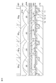
- FIG. 1 is a schematic plan view of the display device according to the first aspect.
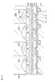
- FIG. 2 is a schematic partial cross-sectional view of the display device according to the first aspect.
- FIG. 3A and FIG. 3B are schematic plan views for explaining the arrangement relationship of various constituent elements that form a pixel.
- FIG. 3A shows the arrangement relationship of the anode electrodes
- FIG. 3B shows the arrangement relationship of the first microlenses.
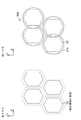
- FIG. 4A and FIG. 4B are schematic plan views for explaining the arrangement relationship of various constituent elements which form the pixel, following FIG. 3B.
- FIG. 4A shows the positional relationship of the color filters
- FIG. 4B shows the positional relationship of the second microlenses.
- FIG. 5A and FIG. 5B are schematic diagrams for explaining light collection by a lens.
- FIG. 5A is a schematic diagram of how light is condensed by a single lens.
- FIG. 5B is a schematic diagram of how light is condensed by the two lenses.
- FIG. 6 is a schematic partial cross-sectional view of a display device according to a reference example.
- 7A and 7B are schematic partial end views for explaining the method for manufacturing the display device according to the first aspect.
- 8A and 8B are schematic partial end views for explaining the method for manufacturing the display device according to the first mode, following FIG. 7B.
- FIG. 9 is a schematic partial end view for explaining the manufacturing method of the display device according to the first aspect, following FIG. 8B.
- FIG. 10 is a schematic partial end view for explaining the method for manufacturing the display device according to the first aspect, following FIG. 9.
- FIG. 9 is a schematic partial end view for explaining the manufacturing method of the display device according to the first aspect, following FIG. 9.
- FIG. 9 is a schematic partial end view for explaining the method for manufacturing the display device according to the first aspect,
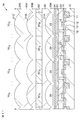
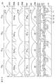
- FIG. 11 is a schematic partial cross-sectional view of a display device according to a first modification of the first aspect.
- FIG. 12 is a schematic partial cross-sectional view of a display device according to a second modification of the first aspect.
- FIG. 13 is a schematic partial cross-sectional view of a display device according to a third modification of the first aspect.
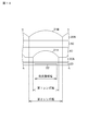
- FIG. 14 is a schematic cross-sectional view for explaining the relationship between the light emitting region width and the lens width.
- FIG. 15A and FIG. 15B are schematic plan views for explaining the arrangement relationship of various constituent elements in the pixel of the modified example.
- FIG. 15A shows the arrangement relationship of the anode electrodes
- FIG. 15B shows the arrangement relationship of the first microlenses.
- 16A and 16B are schematic plan views for explaining the arrangement relationship of various components in the pixel of the modified example subsequent to FIG. 15B.
- 16A shows the positional relationship of the color filters
- FIG. 16B shows the positional relationship of the second microlenses.
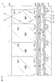
- 17A and 17B are schematic diagrams of a display device according to the second aspect.
- 17A shows a schematic plan view of the display device
- FIG. 17B shows a schematic cross-sectional view of the display device.
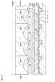
- FIG. 18 is a schematic partial cross-sectional view of the display device according to the second aspect.
- FIG. 19 is a schematic diagram for explaining the reflection of light in the light guide section.
- 20A, 20B, and 20C are schematic partial end views for explaining the method for manufacturing the display device according to the second aspect.
- 21A and 21B are schematic views for explaining the method for manufacturing the display device according to the second mode, following FIG. 20C.
- 21A shows a schematic plan view of the counter substrate
- FIG. 21B shows a schematic cross-sectional view of the counter substrate.
- 22A and 22B are schematic partial end views for explaining the manufacturing method of the display device according to the second mode, following FIG. 21B.
- 23A, 23B, and 23C are schematic partial end views for explaining another example of the process.
- FIG. 24 is a schematic partial cross-sectional view of the display device according to the first modification of the second aspect.
- 25A, 25B, and 25C are schematic partial end views for explaining the method for manufacturing the display device according to the first modification of the second aspect.
- 26A, 26B, and 26C are schematic partial end views for explaining the method for manufacturing the display device according to the first modified example of the second aspect, following FIG. 25C.
- 27A, 27B, and 27C are schematic partial end views for explaining another example of the process.
- FIG. 28 is a schematic partial cross-sectional view of the display device according to the third embodiment.
- 29A and 29B are schematic partial end views for explaining the method for manufacturing the display device according to the third embodiment.
- FIG. 30 is a schematic partial end view for explaining the manufacturing method of the display device according to the third embodiment, following FIG. 29B.
- FIG. 31 is a schematic partial end view for explaining the method for manufacturing the display device according to the third embodiment, following FIG. 30.
- FIG. 32 is a schematic partial end view for explaining the manufacturing method of the display device according to the third embodiment, following FIG. 31.
- FIG. 33 is a schematic partial end view for explaining the manufacturing method of the display device according to the third embodiment, following FIG. 32.
- 34 is a schematic partial end view for explaining the manufacturing method of the display device according to the third embodiment, following FIG. 33.
- FIG. 35 is a schematic partial end view for explaining the method for manufacturing the display device according to the third embodiment, following FIG. 34.
- FIG. 36 is a schematic partial end view for explaining the manufacturing method of the display device according to the third embodiment, following FIG. 35.
- FIG. 37 is a schematic partial end view for explaining the manufacturing method of the display device according to the third embodiment, following FIG. 36.
- FIG. 38 is a schematic partial end view for explaining the manufacturing method of the display device according to the third embodiment, following FIG. 37.
- FIG. 39 is a schematic partial cross-sectional view of the display device according to the first modified example of the third embodiment.
- FIG. 40 is a schematic partial cross-sectional view of the display device according to the second modified example of the third embodiment.
- FIG. 41 is a schematic partial cross-sectional view of a display device according to a third modified example of the third embodiment.
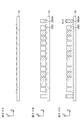
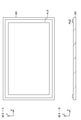
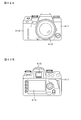
- 42A and 42B are external views of an interchangeable-lens single-lens reflex type digital still camera. 42A shows a front view and FIG. 42B shows a rear view.
- FIG. 43 is an external view of the head mounted display.
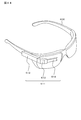
- FIG. 44 is an external view of a see-through head-mounted display.
- the display device is A plurality of light emitting units arranged in a two-dimensional matrix on the substrate, A first lens unit disposed on the plurality of light emitting units and having a first microlens corresponding to each light emitting unit; A second lens portion arranged on the first lens portion and provided with a second microlens corresponding to each light emitting portion; Contains at least.
- a color filter may be arranged between the first microlens and the second microlens.
- the microlens can be made of a known colorless transparent material.
- the microlens can be formed by a known method such as exposure using a gray tone mask, melt flow, dry etching, or the like.
- the color filter may be composed of a well-known color resist material to which a colorant composed of a desired pigment or dye is added. In some cases, it is possible to select a material to which a coloring material is not added as a color filter and set the corresponding pixel as a white display pixel.
- the third lens unit disposed on the second lens unit and including the third microlens corresponding to each light emitting unit Can be further included.
- a color filter may be arranged between the first microlens and the second microlens and between the second microlens and the third microlens.
- the refractive index of the material forming the first microlens is larger than the refractive index of the material forming the second microlens. can do.
- the color filter is arranged between the first microlens and the second microlens, and the refractive index of the optical material forming the color filter is greater than the refractive index of the optical material forming the first microlens. It can be made small and has a refractive index of the optical material of the second microlens or more.
- the first microlenses may be made of an inorganic material, and the second microlenses may be made of an organic material.
- the refractive index of the constituent material used in the present disclosure can be obtained by measuring using, for example, an ellipsometer.
- the display device is A plurality of light emitting units arranged in a two-dimensional matrix on the substrate, and A columnar light guide section that is arranged on the plurality of light emitting sections and corresponds to each light emitting section, Contains A partition wall portion is provided between the adjacent light guide portions.
- the display device may be configured such that the boundary surface between the partition wall portion and the light guide portion forms a light reflection surface.
- the light guide section may be formed of a dielectric material.
- the light guide section can be made of an organic material.
- the organic material include acrylic resin materials and organic silicon resins such as polysiloxane.
- the partition wall portion may be provided so as to have a smaller refractive index than the light guide portion.
- the partition wall portion may be formed as a space.
- the space may be in a state in which the pressure is kept lower than the standard atmospheric pressure in a practical vacuum state, or may be in a state occupied by the atmosphere or a gas such as nitrogen.
- the partition wall portion may be made of a dielectric material.
- the partition wall portion may be formed of a metal material. It is preferable to select a metal material having a large visible light reflectance, and aluminum (Al), gold (Au), silver (Ag), chromium (Cr), nickel (Ni), or an alloy containing these is selected. It can be illustrated.
- the boundary surface between the partition wall portion and the light guide portion extends in the normal direction of the virtual plane including the plurality of light emitting portions.
- the boundary surface between the partition wall portion and the light guide portion may be configured to extend so as to form a predetermined angle with respect to the normal line direction of the virtual plane including the plurality of light emitting portions.
- the display device including the above-described various preferable configurations includes a transparent substrate arranged to face the substrate, and the substrate is arranged in a two-dimensional matrix. Further, a bonding portion is provided so as to surround the regions of the plurality of light emitting portions, and the substrate and the transparent substrate can be bonded via the bonding portion.
- the substrate and the transparent substrate with plasma in a vacuum to activate the surface of the bonding portion, and then bond these in a vacuum.
- the height of the joint is preferably the same as that of the light guide.
- the joint portion and the light guide portion can be formed at the same height.
- the light guide unit includes a first microlens located on the light emitting unit and a second microlens located on the first microlens.
- the configuration may include at least and.
- the partition wall portion is embedded in the filling layer provided between the first microlens and the second microlens, and has a refractive index smaller than that of the filling layer.
- the color filter is arranged between the light emitting unit and the first microlens, between the first microlens and the second microlens, or on the second microlens. be able to.
- examples of the light emitting unit include an organic electroluminescence light emitting unit, an LED light emitting unit, and a semiconductor laser light emitting unit. These light emitting parts can be configured using known materials and methods. From the viewpoint of configuring a flat-panel display device, it is particularly preferable that the light emitting unit is composed of an organic electroluminescent light emitting unit.
- the organic electroluminescence light emitting portion is a so-called top emission type.
- the organic electroluminescence light emitting section can be composed of an anode electrode, a hole transport layer, a light emitting layer, an electron transport layer, a cathode electrode and the like.
- the display device is to display in color, it can be configured to combine a white light emitting unit and a color filter.
- the organic layer including the hole transport layer, the light emitting layer, the electron transport layer, and the like can be shared by a plurality of pixels. Therefore, it is not necessary to separately paint the organic layer for each pixel.
- the red light emitting organic layer, the green light emitting organic layer, and the blue light emitting organic layer may be separately painted according to the pixel. In this configuration, the finer the pixel pitch, the more difficult it is to individually paint. Therefore, in a display device in which the pixel pitch is in units of micrometers, it is preferable that the white light emitting section and the color filter are combined.
- the organic electroluminescent light emitting unit that emits white light may have a structure in which the organic layer has a laminated structure including a red light emitting layer, a green light emitting layer, and a blue light emitting layer, for example.
- the organic layer has a laminated structure including a blue light emitting layer that emits blue light and a yellow light emitting layer that emits yellow light, or a laminated structure that includes a blue light emitting layer that emits blue light and an orange light emitting layer that emits orange light.
- the material forming the organic layer is not particularly limited, and known materials can be used.
- anode electrode of the organic electroluminescence light emitting portion for example, platinum (Pt), gold (Au), silver (Ag), chromium (Cr), tungsten (W), nickel (Ni), aluminum (Al). , Copper (Cu), iron (Fe), cobalt (Co), tantalum (Ta), and other metals or alloys, indium-tin oxide (ITO, Indium Tin Oxide, Sn-doped In 2 O 3 , crystalline ITO, and Examples thereof include transparent conductive materials such as amorphous ITO) and indium-zinc oxide (IZO, Indium Zinc Oxide).
- a conductive material is preferable as a material forming the cathode electrode of the organic electroluminescence light-emitting portion so that emitted light can be transmitted and electrons can be efficiently injected into the organic layer.
- a metal such as aluminum (Al), silver (Ag), magnesium (Mg), calcium (Ca), sodium (Na), strontium (Sr), Mg-Ag alloy, Mg-Ca alloy, Al-Li alloy, or the like. Mention may be made of alloys.
- a drive unit for driving the light emitting unit is provided below, but not limited to, the base on which the light emitting unit is arranged.
- the drive circuit can be composed of, for example, a transistor (specifically, for example, a MOSFET) formed on a silicon semiconductor substrate forming the substrate, or a thin film transistor (TFT) provided on various substrates forming the substrate. . It is possible to adopt a form in which the transistor forming the drive circuit and the light emitting portion are connected via a contact hole (contact plug) formed in the substrate or the like.
- the drive circuit can have a known circuit configuration.
- the pixel arrangement is not particularly limited as long as it does not hinder the implementation of the display device of the present disclosure.
- Examples of the pixel array include a square array, a delta array, and a stripe array.
- FIG. 2 which will be described later, shows a cross-sectional structure of the display device, but does not show ratios such as width, height, and thickness.
- the first embodiment relates to a display device according to the first aspect of the present disclosure.
- FIG. 1 is a conceptual diagram of a display device according to the first embodiment.
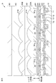
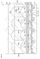
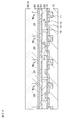
- FIG. 2 is a schematic partial cross-sectional view of the display device according to the first aspect.
- the display device 1 includes a plurality of light emitting units 25 arranged on a substrate 10 in a two-dimensional matrix.
- the light emitting unit 25 is arranged so as to correspond to each pixel 70 of the display device 1.
- the light emitting section 25 is composed of an organic electroluminescence element. The configuration of the light emitting unit 25 will be described later in detail.
- the display device 1 includes a transparent substrate 90 arranged to face the substrate 10.
- Reference numeral 80 indicates a joint portion between the substrate 10 and the transparent substrate 90, which is provided so as to surround the display area.
- the display device 1 is arranged on the plurality of light emitting units 25, and includes a first lens unit 30A including a first microlens 31A corresponding to each light emitting unit 25, and a first lens unit.
- the second lens unit 30B which is disposed on 30A and has the second microlenses 31B corresponding to each light emitting unit 25, is included.
- the first microlens 31A and the second microlens 31B are formed as convex lenses having a convex shape on the light emitting side.
- the shape of the microlens is the shape of a convex lens on the light emitting side, but this is an example, and it suffices if it can have a refracting function as a lens as shown in this example. Even a shape such as a shape is sufficient. Therefore, the shape of the microlens is not limited to the shape shown.
- the color filter 50 is arranged between the first microlens 31A and the second microlens 31B. More specifically, the flattening film 40 is provided on the first microlens 31A, and the color filter 50 is arranged thereon. Then, the second microlens 31B is arranged on the color filter 50.
- the pixel 70 includes the light emitting unit 25, and the first microlens 31A, the color filter 50, and the second microlens 31B corresponding to the light emitting unit 25.
- the red color filter, the green color filter, and the blue color filter are represented by reference numerals 50 R , 50 G , and 50 B , respectively.
- the red display pixel, the green display pixel, and the blue display pixel are represented by reference numerals 70 R , 70 G , and 70 B.
- the refractive index of the material forming the first microlens 31A is larger than the refractive index of the material forming the second microlens 31B. Further, the refractive index of the optical material forming the color filter 50 is smaller than the refractive index of the optical material forming the first microlens 31A, and is equal to or higher than the refractive index of the optical material forming the second microlens 31B.
- the first microlens 31A is made of an inorganic material
- the second microlens 31B is made of an organic material.
- the first microlens 31A is made of silicon nitride (having a refractive index of about 1.8)
- the color filter 50 and the flattening film 40 are made of an acrylic resin material (having a refractive index of 1.4 to 1.4).
- the second microlens 31B is formed by selecting an acrylic resin material having a refractive index smaller than or the same as that of the color filter 50.
- Reference numeral 60 is a sealing resin layer provided between the second microlens 31B and the transparent substrate 90.
- a thermosetting adhesive such as an acrylic adhesive, an epoxy adhesive, a urethane adhesive, a silicone adhesive, or a cyanoacrylate adhesive, or an ultraviolet curable adhesive is used. Can be mentioned.
- the refractive index of the sealing resin layer 60 is preferably smaller than that of the optical material forming the second microlens 31B.
- the drive circuit that drives the light emitting unit 25 is composed of a MOSFET or the like formed on a silicon semiconductor substrate corresponding to the substrate 10.
- a transistor formed of a MOSFET includes a gate insulating layer 14 formed on a substrate 10, a gate electrode 15 formed on the gate insulating layer 14, a source / drain region 12 formed on the substrate 10, and a source / drain region 12. And the element isolation region 11 surrounding the channel formation region 13 and the source / drain regions 12.
- Reference numeral 20 is a flattening film which covers the entire surface including the gate electrode 15.
- the anode electrode 22 arranged corresponding to each light emitting portion 25 is formed on the flattening film 20.
- the anode electrode 22 and the transistor are electrically connected via a contact plug 21 provided on the flattening film 20.
- An organic layer 23 that emits white light is formed on the entire surface including the anode electrode 22.
- the organic layer 23 has a laminated structure of a red light emitting layer, a green light emitting layer, and a blue light emitting layer.
- the organic layer 23 is formed by laminating a plurality of material layers, it is shown as a single layer in the drawing.
- the cathode electrode 24, which is arranged as a common electrode for each light emitting unit 25, is formed on the organic layer 23.
- the ground potential is supplied to the cathode electrode 24.
- the red light emitting organic layer, the green light emitting organic layer, and the blue light emitting organic layer may be separately coated according to the pixel.
- the portion of the organic layer 23 located on the anode electrode 22 emits light.
- the light emitting section 25 is composed of an organic electroluminescence element.
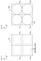
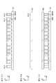
- FIG. 3A and FIG. 3B are schematic plan views for explaining the arrangement relationship of various constituent elements that form a pixel.
- FIG. 3A shows the arrangement relationship of the anode electrodes
- FIG. 3B shows the arrangement relationship of the first microlenses.
- FIG. 4A and FIG. 4B are schematic plan views for explaining the arrangement relationship of various constituent elements which form the pixel, following FIG. 3B.
- FIG. 4A shows the positional relationship of the color filters
- FIG. 4B shows the positional relationship of the second microlenses.
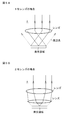
- FIGS. 5A and 5B are schematic diagrams for explaining light collection by a lens.
- FIG. 5A is a schematic diagram of how light is condensed by a single lens.
- FIG. 5B is a schematic diagram of how light is condensed by the two lenses.
- the light emitting area of the light emitting unit 25 is not a dot shape but a surface shape. As shown in FIG. 5A, in the case of a single lens, the light from the peripheral portion of the light emitting region reaches a large extent outside the corresponding lens. Therefore, there is a limit in improving the light extraction efficiency, and the suppression of color mixture between adjacent pixels becomes insufficient.
- the light from the peripheral part of the light emitting area can be sufficiently guided to the corresponding lens. Therefore, it is advantageous over FIG. 5A in terms of light extraction efficiency and suppression of color mixture. Further, as is clear from FIG. 5B, qualitatively, it is preferable to bring the front lens of the double lens close to the light emitting region.
- the first microlens 31A corresponding to each light emitting unit 25 and the second microlens 31B arranged on the first lens unit 30A are arranged. Then, the color filter 50 is arranged between the first microlens 31A and the second microlens 31B. According to this configuration, the first microlens 31A is arranged close to the light emitting unit 25.
- the color filter 50 may be arranged in a lower layer, but it is disadvantageous in that the first microlens 31A is arranged close to the light emitting section 25. This will be described with reference to FIG.
- FIG. 6 is a schematic partial cross-sectional view of a display device according to a reference example.
- the color filter 50 is formed adjacent to the light emitting unit 25, and the first microlens 31A and the second microlens 31B are arranged thereon. In this case, since the color filter 50 is located between the first microlens 31A and the light emitting unit 25, the distance between the incident surface and the light emitting surface of the first microlens 31A becomes longer than that shown in FIG.
- the first microlens 31A is arranged close to the light emitting unit 25. Therefore, the condensing power of the first microlenses 31A is sufficiently exerted, which is advantageous in terms of improving the light extraction efficiency and suppressing color mixing between adjacent pixels.
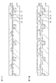
- FIGS. 7A, 7B, 8A, 8B, 9 and 10 are schematic partial end views of a substrate and the like.
- Step-100 First, a MOSFET or the like that serves as a drive circuit for the light emitting unit 25 is formed on the substrate 10, and the flattening film 20 is formed thereon (see FIG. 7A).
- Step-110 Next, an opening is formed in the flattening film 20 at a position where the contact plug 21 is arranged, and a conductive material layer forming the anode electrode 22 is formed on the entire surface including the opening. Then, the conductive material layer is patterned to form the anode electrode 22 on the flattening film 20 (see FIG. 7B).
- the organic layer 23 is formed on the anode electrode 22 and the flattening film 20 by a PVD method such as a vacuum deposition method or a sputtering method, a coating method such as a spin coating method, a die coating method, or the like.
- the cathode electrode 24 is formed on the entire surface based on, for example, a vacuum evaporation method (see FIG. 8A).
- Step-130 Next, the first lens portion 30A having the first microlenses 31A corresponding to each light emitting portion 25 is formed on the entire surface (see FIG. 8B).
- Step-140 After that, the flattening film 40 is formed on the entire surface. Then, the color filter 50 is formed thereon by a known method (see FIG. 9).
- the second lens portion 30B having the second microlenses 31B corresponding to the respective light emitting portions 25 is formed on the entire surface (see FIG. 10).
- the transparent substrate 90 is attached via the sealing resin layer 60 made of, for example, an acrylic adhesive. In this way, the display device 1 shown in FIG. 2 can be obtained.
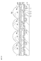
- FIG. 11 is a schematic partial cross-sectional view of a display device according to a first modification of the first aspect.
- the display device 1A according to the first modified example is configured to further include a third lens section that is disposed on the second lens section and that includes a third microlens corresponding to each light emitting section 25. More specifically, the display device 1 shown in FIG. 2 has a configuration in which a third lens portion 30C including a third microlens 31C is further disposed on the second lens portion 30B.
- the sealing resin layer 60 and the transparent substrate 90 are not shown in FIG. 11. The same applies to FIGS. 12 and 13 described later.
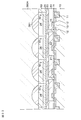
- FIG. 12 is a schematic partial cross-sectional view of a display device according to a second modification of the first aspect.
- the display device 1B according to the second modification has a configuration in which color filters are arranged between the first microlens and the second microlens and between the second microlens and the third microlens. More specifically, in the display device 1B shown in FIG. 11, a color filter 50A is further arranged between the second microlens 31B and the third microlens 31C.
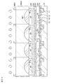
- FIG. 13 is a schematic partial cross-sectional view of a display device according to a third modification of the first aspect.
- the display device 1C according to the third modification has a configuration in which the flattening film 40 is omitted and the color filter 50 is formed in the display device 1 shown in FIG. This configuration can further improve the chromaticity viewing angle characteristic.
- FIG. 14 is a schematic cross-sectional view for explaining the relationship between the light emitting region width and the lens width.
- the width of the first microlens is equal to or larger than the width of the light emitting region and the width of the second microlens is equal to or larger than the width of the first microlens.
- the pixels may be arranged in a manner other than the square arrangement, for example.
- the arrangement of pixels in a modified delta arrangement is shown in the figure.
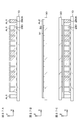
- FIG. 15A and FIG. 15B are schematic plan views for explaining the arrangement relationship of various constituent elements in the pixel of the modified example.
- FIG. 15A shows the arrangement relationship of the anode electrodes
- FIG. 15B shows the arrangement relationship of the first microlenses.
- 16A and 16B are schematic plan views for explaining the arrangement relationship of various components in the pixel of the modified example subsequent to FIG. 15B.
- 16A shows the positional relationship of the color filters
- FIG. 16B shows the positional relationship of the second microlenses.
- the second embodiment relates to a display device according to the second aspect of the present disclosure.
- 17A and 17B are schematic diagrams of a display device according to the second aspect.
- 17A shows a schematic plan view of the display device
- FIG. 17B shows a schematic cross-sectional view of the display device.
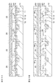
- FIG. 18 is a schematic partial cross-sectional view of the display device according to the second aspect.
- the display device 2 includes a plurality of light emitting units 25 arranged on the substrate 10 in a two-dimensional matrix.
- the light emitting unit 25 is arranged so as to correspond to each pixel 70 of the display device 2.
- the display device 2 includes a transparent substrate 90 arranged to face the substrate 10.
- Reference numeral 280A indicates a joint portion between the substrate 10 and the transparent substrate 90, which is provided so as to surround the display area.
- the display device 2 includes a column-shaped light guide unit 280 which is disposed on the plurality of light emitting units 25 and corresponds to each light emitting unit 25.
- a partition wall BW is provided between the light guide portions 280 adjacent to each other.
- the color filter 50 is formed adjacent to the light emitting unit 25, and the light guide unit 280 is provided on the color filter 50.
- the structure of the substrate 10 to the color filter 50 that is formed is the same as the structure described in the first embodiment, and thus the description thereof is omitted.
- the partition wall portion BW is provided so as to have a smaller refractive index than the light guide portion 280, and the boundary surface between the partition wall portion BW and the light guide portion 280 forms a light reflection surface. That is, when the light from the light emitting unit 25 enters the boundary surface from the light guide unit 280 beyond the critical angle, the light is totally reflected and guided to the observer side. Therefore, it is possible to improve the light extraction efficiency and suppress color mixture between adjacent pixels.
- the partition wall portion BW is formed as a space.
- the light guide 280 is made of a dielectric material. More specifically, the light guide portion 280 is formed of an organic material such as an acrylic resin material or an organic silicone resin material such as polysiloxane.
- a boundary surface between the partition wall portion BW and the light guide portion 280 is formed so as to extend in a normal direction of an imaginary plane including the plurality of light emitting portions 25. In some cases, the boundary surface between the partition wall portion BW and the light guide portion 280 is formed so as to extend at a predetermined angle with respect to the normal direction of the virtual plane including the plurality of light emitting portions 25. Good.
- FIG. 19 is a schematic diagram for explaining light reflection in the light guide section.
- the refractive index of the partition wall BW and the refractive index of the space are both represented by reference numeral n air
- the refractive index of the light guide portion 280 is represented by reference numeral n 1
- the refractive index of the transparent substrate 90 is represented by reference numeral n 2 .
- the refractive index n air 1.
- the substrate 10 of the display device 2 is provided with the joint portion 280A arranged so as to surround the region of the plurality of light emitting portions 25 arranged in the two-dimensional matrix.
- the height of the joint portion 280A is the same as that of the light guide portion 280. More specifically, the joint part 280A and the light guide part 280 are formed by patterning the same material layer.
- the display device 2 also has an advantage that it is easy to narrow the frame.
- the substrate 10 and the transparent substrate 90 are sealed with frit glass or the like, for example, melting the frit glass affects the organic layer 23, and it is difficult to apply the frit glass in a narrow width. For some reasons, there was a limit to narrowing the frame. Further, even if the materials are bonded at room temperature under a low pressure condition such as vacuum, if this is performed without the light guide section 280, the substrate 10 and the transparent substrate 90 will be deformed because the internal pressure is low. Further, since it is hollow, the light extraction efficiency is reduced.
- the display device 2 even if they are bonded at room temperature under a low pressure condition such as a vacuum, the gap between the substrate 10 and the transparent substrate 90 is maintained by the large number of light guide portions 280. Therefore, it is possible to prevent the substrate 10 and the transparent substrate 90 from being deformed while achieving a narrow frame.
- Step-200 the drive circuit of the light emitting unit 25, the light emitting unit 25, the color filter 50, and the like are formed on the substrate 10 (see FIG. 20A). Note that, for convenience, the transistors, the light emitting unit 25, the color filter 50, and the like that form the drive circuit are illustrated in a simplified manner.
- Step-210 the same material layer that forms the joint portion 280A and the light guide portion 280 is formed on the entire surface, and then the joint portion 280A and the light guide portion 280 are formed by a known patterning technique (see FIG. 20B).
- an inorganic film AL1 is formed on the upper surface of the bonding portion 280A provided on the substrate 10 (see FIG. 20C), and the transparent substrate 90 corresponding to the bonding portion 280A is formed.
- the inorganic film AL2 is formed on the portion (see FIGS. 21A and 21B).
- the inorganic film can be formed, for example, as a thin film of silicon (Si), titanium (Ti), copper (Cu), or the like.
- the inorganic film AL1 of the substrate 10 and the inorganic film AL2 of the transparent substrate 90 are activated.
- they can be activated by irradiating Ar plasma (see FIG. 22A).
- Step-240 Then, the substrate 10 and the transparent substrate 90 are opposed to each other, and room temperature bonding is performed in vacuum (see FIG. 22B). Thereby, the display device 2 can be obtained.
- the space of the partition wall portion BW is under a low pressure condition such as vacuum, and the inorganic film only needs to be formed with a sufficiently thin thickness. Therefore, the upper surface of the light guide portion 280 and the transparent substrate 90 are in close contact with each other.
- the adhesion layer was limitedly formed.
- FIG. 23A, FIG. 23B, and FIG. 23C an outline of a modified example of the method for manufacturing the display device 2 will be described.
- an inorganic film is formed not only on the upper surface of the bonding portion 280A but also on the upper surface of the light guide portion 280 (see FIG. 23A).
- an inorganic film is also formed in a portion of the transparent substrate 90 corresponding to the joint portion 280A and a region surrounded by the joint portion 280A (see FIG. 23B).
- the display device 2 can be obtained by performing the above-mentioned [Step-230] and [Step-240] (see FIG. 23C).
- FIG. 24 is a schematic partial cross-sectional view of a display device according to a first modification of the second aspect.
- the display device 2A according to the second modification has a configuration in which the color filter is arranged between the light guide section and the transparent substrate.
- the outline of the method for manufacturing the display device 2A will be described below with reference to FIGS. 25A, 25B, 25C, 26A, 26B, and 26C.
- the color filter 50 is formed on the transparent substrate 90 (see FIG. 25C).
- a protective layer 291 is formed so as to cover the color filter 50, if necessary. Note that the illustration of the protective layer 291 is omitted in FIG.
- Step-220A By performing the above-mentioned [Step-220], the inorganic film AL1 is formed on the upper surface of the joint 280A provided on the substrate 10 (see FIG. 26A), and the inorganic film AL1 is formed on the portion of the transparent substrate 90 corresponding to the joint 280A.
- Form AL2 (see FIG. 26B).
- the display device 2A it is possible to form an inorganic film not only on the upper surface of the joint portion but also on the upper surface of the light guide portion by performing oblique vapor deposition, for example.
- an outline of a modified example of the method for manufacturing the display device 2A will be described.
- the third embodiment relates to a display device according to the second aspect of the present disclosure.
- FIG. 28 is a schematic partial cross-sectional view of the display device according to the third mode.
- a schematic plan view of the display device according to the third aspect is the same as FIG. 17A referred to in the second embodiment, except that the light guide section 280 is replaced with the light guide section 380, and the joint section 280A is replaced with the joint section 80. Good.
- the display device 3 is arranged on the plurality of light emitting units 25 and includes a columnar light guide unit 380 corresponding to each light emitting unit 25.
- a partition wall portion BW is provided between the light guide portions 380 adjacent to each other.
- the color filter 50 is formed adjacent to the light emitting unit 25, and the light guide unit 380 is provided on the color filter 50.
- the structure of the substrate 10 to the color filter 50 that is formed is the same as the structure described in the first embodiment, and thus the description thereof is omitted.
- the light guide unit 380 includes at least a first microlens 381 located on the light emitting unit 25 and a second microlens located on the first microlens 381.
- the partition wall BW is embedded in the filling layer 382 provided between the first microlens 381 and the second microlens 383, and is provided so as to have a smaller refractive index than the filling layer 382. ing.
- the color filter 50 is arranged between the light emitting unit 25 and the first microlens 381, between the first microlens 381 and the second microlens 383, and on the second microlens 383. Can be configured. In the example shown in FIG. 28, the color filter 50 is arranged between the light emitting unit 25 and the first microlens 381.
- the display device 3 can also be configured such that the boundary surface between the partition wall portion and the light guide portion forms a light reflection surface.
- the reflection may be so-called total reflection or specular reflection.
- the partition wall portion may be formed as a space or may be formed of a dielectric material having a low refractive index.
- the partition can be made of a metal material having a high light reflectance, such as aluminum.
- the advantages of the first embodiment such that the first microlens 381 and the second microlens 383 are used, and the light is reflected by the boundary surface between the partition wall portion and the light guide portion.
- the advantages of the second embodiment such as the above can be obtained together.
- Step-310 Next, a material layer 381A for forming the first microlenses 381 is formed on the entire surface (see FIG. 30), and exposure is performed through the gray tone mask GTM (see FIG. 31). After that, development is performed to obtain the first microlenses 381 (see FIG. 32).
- a filling material layer 382A for forming the light guide section 380 and the partition wall BW is formed on the entire surface (see FIG. 33), and exposure is performed through a mask MSK having an opening corresponding to the light guide section 380. Perform (see FIG. 34). After that, development is performed to obtain the filling layer 382 and the partition wall portion BW (see FIG. 35).
- the partition wall BW is described as a space here, when the partition wall BW is made of a dielectric material or a metal material, the partition wall BW formed as a space may be filled with these materials. Good.
- a material layer 383A for forming the second microlens 383 is formed on the entire surface (see FIG. 36), and exposure is performed through the gray tone mask GTM (see FIG. 37). After that, development is performed to obtain the second microlens 383 (see FIG. 38).
- the display device 3 can be obtained by bonding the substrate 10 and the transparent substrate 90 via the sealing resin layer 60.
- FIG. 39 is a schematic partial cross-sectional view of a display device according to a first modification of the third embodiment.
- FIG. 40 is a schematic partial cross-sectional view of the display device according to the second modified example of the third embodiment.
- the color filter 50 may be arranged on any of the above.
- the color filter 50 is arranged between the second microlens 383 and the transparent substrate 90.
- the color filter 50 is arranged between the first microlens 381 and the second microlens 383.
- the distance between the light emitting unit 25 and the first microlens 381 is short.
- the chromaticity viewing angle is improved, but the light extraction efficiency is slightly reduced.
- the light extraction efficiency can be improved as compared with the configuration shown in FIG.
- the chromaticity viewing angle is slightly reduced.
- the second modification has an advantage that both the light extraction efficiency and the chromaticity viewing angle can be improved.
- FIG. 41 is a schematic partial cross-sectional view of a display device according to a third modification of the third embodiment.
- the second microlens 383 is a concave lens type.
- the second microlens 383 is a convex lens, qualitatively, the front luminance tends to be higher than the peripheral luminance.
- the second microlens 383 it is possible to control the light rays to diverge to the wide viewing angle side of the panel by making the second microlens 383 a concave lens type.
- the display device of the present disclosure described above is used as a display unit (display device) of an electronic device in any field that displays, as an image or a video, a video signal input to the electronic device or a video signal generated in the electronic device.
- a display unit such as a television set, a digital still camera, a laptop personal computer, a mobile terminal device such as a mobile phone, a video camera, a head mounted display (head mounted display), or the like.
- the display device of the present disclosure also includes a module having a sealed configuration.
- a display module formed by attaching a facing portion such as transparent glass to a pixel array portion is applicable.
- the display module may be provided with a circuit unit for inputting / outputting a signal or the like from the outside to the pixel array unit, a flexible printed circuit (FPC), or the like.
- FPC flexible printed circuit
- FIG. 42 is an external view of an interchangeable-lens single-lens reflex type digital still camera.
- FIG. 42A shows its front view
- FIG. 42B shows its rear view.
- the interchangeable-lens single-lens reflex type digital still camera has, for example, an interchangeable photographing lens unit (interchangeable lens) 412 on the front right side of a camera body (camera body) 411, and a photographer holds it on the front left side. It has a grip portion 413 for.
- interchangeable photographing lens unit interchangeable lens
- a monitor 414 is provided at the approximate center of the back surface of the camera body 411.
- a viewfinder (eyepiece window) 415 is provided above the monitor 414. By looking through the viewfinder 415, the photographer can visually recognize the optical image of the subject guided from the taking lens unit 412 and determine the composition.
- the display device of the present disclosure can be used as the viewfinder 415 in the lens interchangeable single-lens reflex type digital still camera configured as described above. That is, the lens interchangeable single-lens reflex type digital still camera according to the present example is manufactured by using the display device of the present disclosure as the viewfinder 415.
- FIG. 43 is an external view of the head mounted display.
- the head mounted display has, for example, ear hooks 512 to be worn on the head of the user, on both sides of a spectacle-shaped display unit 511.
- the display device of the present disclosure can be used as the display unit 511. That is, the head mounted display according to this example is manufactured by using the display device of the present disclosure as the display unit 511.
- FIG. 44 is an external view of a see-through head-mounted display.
- the see-through head mount display 611 includes a main body 612, an arm 613, and a lens barrel 614.
- the body 612 is connected to the arm 613 and the eyeglasses 600. Specifically, an end portion of the main body portion 612 in the long side direction is coupled to the arm 613, and one side surface of the main body portion 612 is coupled to the eyeglasses 600 via a connecting member.
- the main body 612 may be directly attached to the head of the human body.
- the main body part 612 has a control board for controlling the operation of the see-through head mounted display 611 and a display part.
- the arm 613 connects the main body 612 and the lens barrel 614 and supports the lens barrel 614. Specifically, the arm 613 is coupled to the end of the main body 612 and the end of the lens barrel 614, respectively, and fixes the lens barrel 614. Further, the arm 613 incorporates a signal line for communicating data related to an image provided from the main body 612 to the lens barrel 614.
- the lens barrel 614 projects the image light provided from the main body 612 via the arm 613 toward the eyes of the user wearing the see-through head mounted display 611 through the eyepiece lens.
- the display device of the present disclosure can be used for the display portion of the main body portion 612.
- a plurality of light emitting units arranged in a two-dimensional matrix on the substrate A first lens unit disposed on the plurality of light emitting units and having a first microlens corresponding to each light emitting unit; A second lens portion arranged on the first lens portion and provided with a second microlens corresponding to each light emitting portion; Contains at least Display device.
- a color filter is disposed between the first microlens and the second microlens, The display device according to [A1].
- a third lens portion provided on the second lens portion and provided with a third microlens corresponding to each light emitting portion Further includes, The display device according to [A1].
- [A4] Color filters are arranged between the first microlens and the second microlens, and between the second microlens and the third microlens, The display device according to [A3].
- the material forming the first microlens has a higher refractive index than the material forming the second microlens, The display device according to any one of [A1] to [A4].
- a color filter is arranged between the first microlens and the second microlens, The refractive index of the optical material forming the color filter is smaller than the refractive index of the optical material forming the first microlens, and is equal to or more than the refractive index of the optical material forming the second microlens.
- the first microlens is made of an inorganic material
- the second microlens is made of an organic material
- [B1] A plurality of light emitting units arranged in a two-dimensional matrix on the substrate, and A columnar light guide section that is arranged on the plurality of light emitting sections and corresponds to each light emitting section, Contains A partition is provided between the adjacent light guides, Display device.
- the boundary surface between the partition wall portion and the light guide portion forms a light reflection surface, The display device according to [B1].
- the light guide section is made of a dielectric material, The display device according to [B1] or [B2].
- [B4] The light guide section is made of an organic material, The display device according to [B3].
- the partition wall portion is provided so that the refractive index is smaller than that of the light guide portion, The display device according to any one of [B1] to [B4].
- the partition part is formed as a space, The display device according to any one of [B1] to [B5].
- the partition part is made of a dielectric material, The display device according to any one of [B1] to [B6].
- the partition part is made of a metal material, The display device according to [B1].
- a boundary surface between the partition wall portion and the light guide portion extends in a direction normal to a virtual plane including a plurality of light emitting portions, The display device according to any one of [B1] to [B8].
- the boundary surface between the partition wall portion and the light guide portion extends so as to form a predetermined angle with respect to the normal direction of the virtual plane including the plurality of light emitting portions,
- the display device according to any one of [B1] to [B8].
- [B11] Equipped with a transparent substrate arranged to face the substrate, The substrate is provided with a joint portion arranged so as to surround a plurality of light emitting portion regions arranged in a two-dimensional matrix, The substrate and the transparent substrate are bonded via a bonding portion, The display device according to any one of [B1] to [B10].
- the height of the joint is the same as that of the light guide, The display device according to any one of the above [B11].
- the light guide unit includes at least a first microlens located on the light emitting unit and a second microlens located on the first microlens.
- the display device according to any one of [B1] to [B12].
- the partition wall portion is embedded in a filling layer provided between the first microlens and the second microlens, and has a refractive index smaller than that of the filling layer.
- a color filter is arranged between the light emitting unit and the first microlens, between the first microlens and the second microlens, or on the second microlens.
- Flattening film 50, 50 R , 50 G , 50 B , 50 A, 50 A R , 50 A G , 50 A B ... color filter, 60 ... sealing resin layer, 70, 70 R, 7 G, 70 B ... pixels, 80 ... junction, 90 ... transparent substrate, 280 ... light guide unit, 280A ... joint, 380 ... guide portion, 381 ... First microlens, 381A ... Material layer for forming first microlens, 382 ... Filling layer, 382A ... Filling material layer, 383 ... Second microlens, 383A ... 2 Material layer for forming microlens, BW ... partition wall portion, AL1, AL2 ... inorganic film, 411 ...
- camera body portion 412 ... photographing lens unit, 413 ... grip portion, 414 ... Monitor, 415 ... Viewfinder, 511 ... Eyeglass-shaped display section, 512 ... Ear rest section, 600 ... Eyeglasses, 611 ... See-through head mount display, 612 ... Body 613 ... arm, 614 ... barrel
Landscapes
- Physics & Mathematics (AREA)
- General Physics & Mathematics (AREA)
- Optics & Photonics (AREA)
- Engineering & Computer Science (AREA)
- Theoretical Computer Science (AREA)
- Electroluminescent Light Sources (AREA)
- Devices For Indicating Variable Information By Combining Individual Elements (AREA)
Abstract
Description
基板に2次元マトリクス状に配置された複数の発光部、
複数の発光部の上に配置され、各発光部に対応した第1マイクロレンズを備えた第1レンズ部、及び、
第1レンズ部の上に配置され、各発光部に対応した第2マイクロレンズを備えた第2レンズ部、
を少なくとも含んでいる、
表示装置である。
基板に2次元マトリクス状に配置された複数の発光部、及び、
複数の発光部の上に配置され、各発光部に対応した柱状の導光部、
を含んでおり、
それぞれ隣接する導光部の間には隔壁部が設けられている、
表示装置である。
1.本開示に係る表示装置、全般に関する説明
2.第1の実施形態
3.第2の実施形態
4.第3の実施形態
5.電子機器の説明、その他
上述したように、本開示の第1の態様に係る表示装置は、
基板に2次元マトリクス状に配置された複数の発光部、
複数の発光部の上に配置され、各発光部に対応した第1マイクロレンズを備えた第1レンズ部、及び、
第1レンズ部の上に配置され、各発光部に対応した第2マイクロレンズを備えた第2レンズ部、
を少なくとも含んでいる。
基板に2次元マトリクス状に配置された複数の発光部、及び、
複数の発光部の上に配置され、各発光部に対応した柱状の導光部、
を含んでおり、
それぞれ隣接する導光部の間には隔壁部が設けられている。
第1の実施形態は、本開示の第1の態様に係る、表示装置に関する。
先ず、基板10に発光部25の駆動回路となるMOSFETなどを形成し、その上に平坦化膜20を形成する(図7A参照)。
次いで、平坦化膜20においてコンタクトプラグ21が配置される位置に開口を形成し、開口を含む全面に、アノード電極22を構成する導電材料層を形成する。その後、導電材料層をパターニングし、平坦化膜20上にアノード電極22を形成する(図7B参照)。
次いで、アノード電極22および平坦化膜20の上に、有機層23を、例えば、真空蒸着法やスパッタリング法といったPVD法、スピンコート法やダイコート法等のコーティング法等によって成膜する。その後、例えば真空蒸着法等に基づき、全面にカソード電極24を形成する(図8A参照)。
次いで、全面に、各発光部25に対応した第1マイクロレンズ31Aを備えた第1レンズ部30Aを形成する(図8B参照)。
その後、全面に平坦化膜40を形成する。次いで、周知の方法で、その上に、カラーフィルタ50を形成する(図9参照)。
その後、全面に、各発光部25に対応した第2マイクロレンズ31Bを備えた第2レンズ部30Bを形成する(図10参照)。次いで、例えばアクリル系接着剤から成る封止樹脂層60を介して透明基板90を貼り合わせる。こうして、図2に示した表示装置1を得ることができる。
第2の実施形態は、本開示の第2の態様に係る、表示装置に関する。
Sin(π/2-θ1)/Sin(θ2)=n2/n1
と表される。この式を変形すると、
Sin(θ2)=(n1/n2)×(1-Sin2(θ1))1/2
が得られる、これを上述したSin(θ2)<1/n2に代入して整理すると、
Sin(θ1)>(1-(1/n1)2)1/2
となる。従って、1/n1=(1-(1/n1)2)1/2となるように設定すると取り出せる光量が最大となる。よって、n1=21/2といった値にすることが好ましい。
先ず、基板10に発光部25の駆動回路、発光部25、カラーフィルタ50などを形成する(図20A参照)。尚、便宜のため、駆動回路を構成するトランジスタ、発光部25、カラーフィルタ50などは簡易的に示した。
次いで、接合部280Aと導光部280とを構成する同一の材料層を全面に形成し、その後、周知のパターニング技術によって、接合部280Aと導光部280を形成する(図20B参照)。
その後、常温接合時の密着性を向上させるために、基板10に設けられた接合部280Aの上面に無機膜AL1を形成し(図20C参照)、また、接合部280Aに対応する透明基板90の部分に無機膜AL2を形成する(図21A、図21B参照)。無機膜は、例えば、シリコン(Si)、チタン(Ti)、銅(Cu)などの薄膜として形成することができる。
次いで、基板10の無機膜AL1と透明基板90の無機膜AL2を活性化する。例えば、Arプラズマを照射することによって、これらを活性化することができる(図22A参照)。
その後、基板10と透明基板90とを対向させ、真空中において常温接合を行う(図22B参照)。これによって、表示装置2を得ることができる。隔壁部BWの空間は真空などの低圧条件下であって、また無機膜は充分に薄い厚さで形成すれば足りるので、導光部280の上面と透明基板90とは密着した状態となる。
先ず、基板10に発光部25の駆動回路、発光部25などを形成する(図25A参照)。次いで、上述した[工程-220]を行い、導光部280と接合部280Aを形成する(図25B参照)。
また、透明基板90上にカラーフィルタ50を形成する(図25C参照)。必要に応じて、カラーフィルタ50を覆うように保護層291を形成する。尚、図24においては、保護層291の図示は省略した。
上述した[工程-220]を行い、基板10に設けられた接合部280Aの上面に無機膜AL1を形成し(図26A参照)、また、接合部280Aに対応する透明基板90の部分に無機膜AL2を形成する(図26B参照)。
上述した[工程-230]および[工程-240]を行うことによって、表示装置2Aを得ることができる(図26C参照)。
第3の実施形態は、本開示の第2の態様に係る、表示装置に関する。
第1の実施形態において説明した[工程-100]ないし[工程-120]を行い、発光部25が形成された基板10を得る(図29A参照)。その後、基板10上にカラーフィルタ50を形成する(図29B参照)。
次いで、全面に、第1マイクロレンズ381を構成するための材料層381Aを成膜し(図30参照)、グレートーンマスクGTMを介して露光を行う(図31参照)。その後、現像を行い、第1マイクロレンズ381を得る(図32参照)。
次いで、全面に、導光部380や隔壁部BWを形成するための充填材料層382Aを成膜し(図33参照)、導光部380に対応する部分が開口したマスクMSKを介して露光を行う(図34参照)。その後、現像を行い、充填層382と、隔壁部BWを得る(図35参照)。尚、ここでは、隔壁部BWは空間であるとして説明するが、誘電材料や金属材料で隔壁部BWを構成する場合には、空間として形成された隔壁部BWにこれらの材料を埋め込むようにすればよい。
次いで、全面に、第2マイクロレンズ383を構成するための材料層383Aを成膜し(図36参照)、グレートーンマスクGTMを介して露光を行う(図37参照)。その後、現像を行い、第2マイクロレンズ383を得る(図38参照)。
次いで、基板10と透明基板90とを、封止樹脂層60を介して貼り合わせることによって、表示装置3を得ることができる。
以上説明した本開示の表示装置は、電子機器に入力された映像信号、若しくは、電子機器内で生成した映像信号を、画像若しくは映像として表示するあらゆる分野の電子機器の表示部(表示装置)として用いることができる。一例として、例えば、テレビジョンセット、デジタルスチルカメラ、ノート型パーソナルコンピュータ、携帯電話機等の携帯端末装置、ビデオカメラ、ヘッドマウントディスプレイ(頭部装着型ディスプレイ)等の表示部として用いることができる。
図42は、レンズ交換式一眼レフレックスタイプのデジタルスチルカメラの外観図であり、図42Aにその正面図を示し、図42Bにその背面図を示す。レンズ交換式一眼レフレックスタイプのデジタルスチルカメラは、例えば、カメラ本体部(カメラボディ)411の正面右側に交換式の撮影レンズユニット(交換レンズ)412を有し、正面左側に撮影者が把持するためのグリップ部413を有している。
図43は、ヘッドマウントディスプレイの外観図である。ヘッドマウントディスプレイは、例えば、眼鏡形の表示部511の両側に、使用者の頭部に装着するための耳掛け部512を有している。このヘッドマウントディスプレイにおいて、その表示部511として本開示の表示装置を用いることができる。すなわち、本例に係るヘッドマウントディスプレイは、その表示部511として本開示の表示装置を用いることによって作製される。
図44は、シースルーヘッドマウントディスプレイの外観図である。シースルーヘッドマウントディスプレイ611は、本体部612、アーム613および鏡筒614で構成される。
なお、本開示の技術は以下のような構成も取ることができる。
基板に2次元マトリクス状に配置された複数の発光部、
複数の発光部の上に配置され、各発光部に対応した第1マイクロレンズを備えた第1レンズ部、及び、
第1レンズ部の上に配置され、各発光部に対応した第2マイクロレンズを備えた第2レンズ部、
を少なくとも含んでいる、
表示装置。
[A2]
第1マイクロレンズと第2マイクロレンズとの間にカラーフィルタが配置されている、
上記[A1]に記載の表示装置。
[A3]
第2レンズ部の上に配置され、各発光部に対応した第3マイクロレンズを備えた第3レンズ部、
を更に含んでいる、
上記[A1]に記載の表示装置。
[A4]
第1マイクロレンズと第2マイクロレンズとの間、及び、第2マイクロレンズと第3マイクロレンズとの間にカラーフィルタが配置されている、
上記[A3]に記載の表示装置。
[A5]
第1マイクロレンズを形成する材料の屈折率は、第2マイクロレンズを形成する材料の屈折率よりも大きい、
上記[A1]ないし[A4]のいずれかに記載の表示装置。
[A6]
第1マイクロレンズと第2マイクロレンズとの間にカラーフィルタが配置されており、
カラーフィルタを形成する光学材料の屈折率は、第1マイクロレンズを形成する光学材料の屈折率より小さく、第2マイクロレンズを形成する光学材料の屈折率以上である、
上記[A5]に記載の表示装置。
[A7]
第1マイクロレンズは無機材料から形成されており、第2マイクロレンズは有機材料から形成されている、
上記[A5]または[A6]に記載の表示装置。
基板に2次元マトリクス状に配置された複数の発光部、及び、
複数の発光部の上に配置され、各発光部に対応した柱状の導光部、
を含んでおり、
それぞれ隣接する導光部の間には隔壁部が設けられている、
表示装置。
[B2]
隔壁部と導光部との境界面が光反射面を形成する、
上記[B1]に記載の表示装置。
[B3]
導光部は誘電材料から形成されている、
上記[B1]または[B2]に記載の表示装置。
[B4]
導光部は有機材料から形成されている、
上記[B3]に記載の表示装置。
[B5]
隔壁部は導光部よりも屈折率が小さくなるように設けられている、
上記[B1]ないし[B4]のいずれかに記載の表示装置。
[B6]
隔壁部は空間として形成されている、
上記[B1]ないし[B5]のいずれかに記載の表示装置。
[B7]
隔壁部は誘電材料から形成されている、
上記[B1]ないし[B6]のいずれかに記載の表示装置。
[B8]
隔壁部は金属材料から形成されている、
上記[B1]に記載の表示装置。
[B9]
隔壁部と導光部との境界面は、複数の発光部を含む仮想平面の法線方向に伸びる、
上記[B1]ないし[B8]のいずれかに記載の表示装置。
[B10]
隔壁部と導光部との境界面は、複数の発光部を含む仮想平面の法線方向に対して所定の角度を成すように伸びる、
上記[B1]ないし[B8]のいずれかに記載の表示装置。
[B11]
基板に対向して配置される透明基板を備えており、
基板には、2次元マトリクス状に配置された複数の発光部の領域を囲むように配置された接合部が設けられており、
基板と透明基板とは、接合部を介して接合されている、
上記[B1]ないし[B10]のいずれかに記載の表示装置。
[B12]
接合部の高さは、導光部と同じ高さに形成されている、
上記[B11]のいずれかに記載の表示装置。
[B13]
導光部は、発光部上に位置する第1マイクロレンズと、第1マイクロレンズ上に位置する第2マイクロレンズとを少なくとも含んでいる、
上記[B1]ないし[B12]のいずれかに記載の表示装置。
[B14]
隔壁部は、第1マイクロレンズと第2マイクロレンズとの間に設けられた充填層に埋め込まれており、且つ、充填層よりも屈折率が小さくなるように設けられている、
上記[B13]に記載の表示装置。
[B15]
発光部と第1マイクロレンズとの間、第1マイクロレンズと第2マイクロレンズとの間、及び、第2マイクロレンズの上のいずれかに、カラーフィルタが配置されている。
上記[B13]に記載の表示装置。
Claims (22)
- 基板に2次元マトリクス状に配置された複数の発光部、
複数の発光部の上に配置され、各発光部に対応した第1マイクロレンズを備えた第1レンズ部、及び、
第1レンズ部の上に配置され、各発光部に対応した第2マイクロレンズを備えた第2レンズ部、
を少なくとも含んでいる、
表示装置。 - 第1マイクロレンズと第2マイクロレンズとの間にカラーフィルタが配置されている、
請求項1に記載の表示装置。 - 第2レンズ部の上に配置され、各発光部に対応した第3マイクロレンズを備えた第3レンズ部、
を更に含んでいる、
請求項1に記載の表示装置。 - 第1マイクロレンズと第2マイクロレンズとの間、及び、第2マイクロレンズと第3マイクロレンズとの間にカラーフィルタが配置されている、
請求項3に記載の表示装置。 - 第1マイクロレンズを形成する材料の屈折率は、第2マイクロレンズを形成する材料の屈折率よりも大きい、
請求項1に記載の表示装置。 - 第1マイクロレンズと第2マイクロレンズとの間にカラーフィルタが配置されており、
カラーフィルタを形成する光学材料の屈折率は、第1マイクロレンズを形成する光学材料の屈折率より小さく、第2マイクロレンズを形成する光学材料の屈折率以上である、
請求項5に記載の表示装置。 - 第1マイクロレンズは無機材料から形成されており、第2マイクロレンズは有機材料から形成されている、
請求項5に記載の表示装置。 - 基板に2次元マトリクス状に配置された複数の発光部、及び、
複数の発光部の上に配置され、各発光部に対応した柱状の導光部、
を含んでおり、
それぞれ隣接する導光部の間には隔壁部が設けられている、
表示装置。 - 隔壁部と導光部との境界面が光反射面を形成する、
請求項8に記載の表示装置。 - 導光部は誘電材料から形成されている、
請求項8に記載の表示装置。 - 導光部は有機材料から形成されている、
請求項10に記載の表示装置。 - 隔壁部は導光部よりも屈折率が小さくなるように設けられている、
請求項8に記載の表示装置。 - 隔壁部は空間として形成されている、
請求項8に記載の表示装置。 - 隔壁部は誘電材料から形成されている、
請求項8に記載の表示装置。 - 隔壁部は金属材料から形成されている、
請求項8に記載の表示装置。 - 隔壁部と導光部との境界面は、複数の発光部を含む仮想平面の法線方向に伸びる、
請求項8に記載の表示装置。 - 隔壁部と導光部との境界面は、複数の発光部を含む仮想平面の法線方向に対して所定の角度を成すように伸びる、
請求項8に記載の表示装置。 - 基板に対向して配置される透明基板を備えており、
基板には、2次元マトリクス状に配置された複数の発光部の領域を囲むように配置された接合部が設けられており、
基板と透明基板とは、接合部を介して接合されている、
請求項8に記載の表示装置。 - 接合部の高さは、導光部と同じ高さに形成されている、
請求項18に記載の表示装置。 - 導光部は、発光部上に位置する第1マイクロレンズと、第1マイクロレンズ上に位置する第2マイクロレンズとを少なくとも含んでいる、
請求項8に記載の表示装置。 - 隔壁部は、第1マイクロレンズと第2マイクロレンズとの間に設けられた充填層に埋め込まれており、且つ、充填層よりも屈折率が小さくなるように設けられている、
請求項20に記載の表示装置。 - 発光部と第1マイクロレンズとの間、第1マイクロレンズと第2マイクロレンズとの間、及び、第2マイクロレンズの上のいずれかに、カラーフィルタが配置されている。
請求項20に記載の表示装置。
Priority Applications (5)
| Application Number | Priority Date | Filing Date | Title |
|---|---|---|---|
| CN201980066970.2A CN112840744B (zh) | 2018-10-16 | 2019-09-18 | 显示装置 |
| DE112019005173.3T DE112019005173T5 (de) | 2018-10-16 | 2019-09-18 | Anzeigevorrichtung |
| KR1020217009592A KR20210069050A (ko) | 2018-10-16 | 2019-09-18 | 표시 장치 |
| JP2020552976A JPWO2020080022A1 (ja) | 2018-10-16 | 2019-09-18 | 表示装置 |
| US17/279,317 US20210399264A1 (en) | 2018-10-16 | 2019-09-18 | Display device |
Applications Claiming Priority (2)
| Application Number | Priority Date | Filing Date | Title |
|---|---|---|---|
| JP2018194868 | 2018-10-16 | ||
| JP2018-194868 | 2018-10-16 |
Publications (1)
| Publication Number | Publication Date |
|---|---|
| WO2020080022A1 true WO2020080022A1 (ja) | 2020-04-23 |
Family
ID=70283484
Family Applications (1)
| Application Number | Title | Priority Date | Filing Date |
|---|---|---|---|
| PCT/JP2019/036557 Ceased WO2020080022A1 (ja) | 2018-10-16 | 2019-09-18 | 表示装置 |
Country Status (6)
| Country | Link |
|---|---|
| US (1) | US20210399264A1 (ja) |
| JP (1) | JPWO2020080022A1 (ja) |
| KR (1) | KR20210069050A (ja) |
| CN (1) | CN112840744B (ja) |
| DE (1) | DE112019005173T5 (ja) |
| WO (1) | WO2020080022A1 (ja) |
Cited By (13)
| Publication number | Priority date | Publication date | Assignee | Title |
|---|---|---|---|---|
| WO2022004652A1 (ja) * | 2020-06-29 | 2022-01-06 | 凸版印刷株式会社 | カラーフィルタおよび表示装置 |
| JP2022011076A (ja) * | 2020-06-29 | 2022-01-17 | 凸版印刷株式会社 | カラーフィルタおよび表示装置 |
| JP2022011075A (ja) * | 2020-06-29 | 2022-01-17 | 凸版印刷株式会社 | カラーフィルタおよび表示装置 |
| JPWO2022044980A1 (ja) * | 2020-08-28 | 2022-03-03 | ||
| JPWO2022080205A1 (ja) * | 2020-10-13 | 2022-04-21 | ||
| JP2022071516A (ja) * | 2020-10-28 | 2022-05-16 | キヤノン株式会社 | 発光装置、表示装置、撮像装置、及び、電子機器 |
| JPWO2022149554A1 (ja) * | 2021-01-08 | 2022-07-14 | ||
| CN115702505A (zh) * | 2020-06-12 | 2023-02-14 | 苹果公司 | 显示设备 |
| US20230097317A1 (en) * | 2020-02-26 | 2023-03-30 | Sony Semiconductor Solutions Corporation | Light emitting element, display device, and method for manufacturing display device |
| CN115917397A (zh) * | 2021-04-30 | 2023-04-04 | 京东方科技集团股份有限公司 | 双栅线阵列基板、显示面板 |
| JP7598907B1 (ja) | 2022-09-21 | 2024-12-12 | ホアウェイ・テクノロジーズ・カンパニー・リミテッド | 有機電界発光素子および有機電界発光ディスプレイ |
| JP2025513139A (ja) * | 2022-04-24 | 2025-04-24 | 京東方科技集團股▲ふん▼有限公司 | 表示装置、表示パネル及びその製造方法 |
| WO2025206044A1 (ja) * | 2024-03-27 | 2025-10-02 | ソニーセミコンダクタソリューションズ株式会社 | 発光装置および画像表示装置 |
Families Citing this family (13)
| Publication number | Priority date | Publication date | Assignee | Title |
|---|---|---|---|---|
| KR102686305B1 (ko) * | 2019-07-02 | 2024-07-19 | 삼성디스플레이 주식회사 | 표시장치 |
| CN112859347A (zh) * | 2021-02-25 | 2021-05-28 | 京东方科技集团股份有限公司 | 近眼显示装置及可穿戴设备 |
| CN113241354B (zh) * | 2021-04-07 | 2022-07-12 | 武汉华星光电技术有限公司 | Oled显示面板及其制备方法 |
| CN113299703B (zh) * | 2021-05-08 | 2022-09-09 | 武汉华星光电技术有限公司 | 显示面板 |
| US20240381746A1 (en) * | 2021-09-09 | 2024-11-14 | Taizhou Guanyu Technology Co., Ltd. | Display device |
| CN116828893A (zh) * | 2021-09-09 | 2023-09-29 | 台州观宇科技有限公司 | 显示设备 |
| CN117337626A (zh) * | 2022-04-27 | 2024-01-02 | 京东方科技集团股份有限公司 | 显示面板、显示装置 |
| US20250031555A1 (en) * | 2022-05-23 | 2025-01-23 | Chengdu Boe Optoelectronics Technology Co., Ltd. | Display panel and display device |
| CN115377326A (zh) * | 2022-08-31 | 2022-11-22 | 京东方科技集团股份有限公司 | 显示基板、显示装置及显示基板的制备方法 |
| WO2024152284A1 (zh) * | 2023-01-19 | 2024-07-25 | 京东方科技集团股份有限公司 | 显示面板和显示装置 |
| KR20250112959A (ko) * | 2024-01-17 | 2025-07-25 | 삼성디스플레이 주식회사 | 표시 장치 및 이의 제조 방법 |
| US20260107618A1 (en) * | 2024-10-15 | 2026-04-16 | Innolux Corporation | Electronic device |
| CN119947515B (zh) * | 2025-01-21 | 2026-03-24 | 昆山国显光电有限公司 | 显示模组和显示装置 |
Citations (4)
| Publication number | Priority date | Publication date | Assignee | Title |
|---|---|---|---|---|
| JPH06250164A (ja) * | 1993-02-26 | 1994-09-09 | Noritake Co Ltd | 導光板および導光板を用いた表示装置 |
| JPH10170860A (ja) * | 1996-12-09 | 1998-06-26 | Olympus Optical Co Ltd | 眼球投影型映像表示装置 |
| JP2012009154A (ja) * | 2010-06-22 | 2012-01-12 | Seiko Epson Corp | 照明装置および表示装置 |
| JP2015206813A (ja) * | 2014-04-17 | 2015-11-19 | セイコーエプソン株式会社 | マイクロレンズアレイ基板、電気光学装置、及び電子機器 |
Family Cites Families (12)
| Publication number | Priority date | Publication date | Assignee | Title |
|---|---|---|---|---|
| JPH0950081A (ja) * | 1995-08-08 | 1997-02-18 | Sony Corp | 透過型表示装置 |
| JP4524843B2 (ja) * | 2000-03-16 | 2010-08-18 | ソニー株式会社 | 直視型表示装置 |
| JP2004342448A (ja) * | 2003-05-15 | 2004-12-02 | Ricoh Opt Ind Co Ltd | 有機elディスプレイ |
| KR100912802B1 (ko) * | 2005-02-28 | 2009-08-18 | 삼성모바일디스플레이주식회사 | 전계발광 디스플레이 장치 |
| JP2008026654A (ja) * | 2006-07-21 | 2008-02-07 | Hitachi Displays Ltd | 立体表示装置 |
| JP2013008663A (ja) * | 2011-05-24 | 2013-01-10 | Canon Inc | 表示装置 |
| JP2013149536A (ja) | 2012-01-23 | 2013-08-01 | Canon Inc | 表示装置 |
| KR102360089B1 (ko) * | 2014-08-05 | 2022-02-09 | 삼성디스플레이 주식회사 | 유기 발광 표시 장치 및 그 제조방법 |
| KR102335812B1 (ko) * | 2014-09-19 | 2021-12-09 | 삼성디스플레이 주식회사 | 유기발광 표시장치 |
| US10529696B2 (en) * | 2016-04-12 | 2020-01-07 | Cree, Inc. | High density pixelated LED and devices and methods thereof |
| US10804499B2 (en) * | 2016-08-19 | 2020-10-13 | Sony Semiconductor Solutions Corporation | Light emitting element, display element, and method for producing light emitting element |
| KR102508724B1 (ko) * | 2018-02-14 | 2023-03-14 | 삼성디스플레이 주식회사 | 지문 센싱 유닛 및 이를 포함하는 표시 장치 |
-
2019
- 2019-09-18 US US17/279,317 patent/US20210399264A1/en not_active Abandoned
- 2019-09-18 JP JP2020552976A patent/JPWO2020080022A1/ja active Pending
- 2019-09-18 DE DE112019005173.3T patent/DE112019005173T5/de active Pending
- 2019-09-18 CN CN201980066970.2A patent/CN112840744B/zh active Active
- 2019-09-18 KR KR1020217009592A patent/KR20210069050A/ko active Pending
- 2019-09-18 WO PCT/JP2019/036557 patent/WO2020080022A1/ja not_active Ceased
Patent Citations (4)
| Publication number | Priority date | Publication date | Assignee | Title |
|---|---|---|---|---|
| JPH06250164A (ja) * | 1993-02-26 | 1994-09-09 | Noritake Co Ltd | 導光板および導光板を用いた表示装置 |
| JPH10170860A (ja) * | 1996-12-09 | 1998-06-26 | Olympus Optical Co Ltd | 眼球投影型映像表示装置 |
| JP2012009154A (ja) * | 2010-06-22 | 2012-01-12 | Seiko Epson Corp | 照明装置および表示装置 |
| JP2015206813A (ja) * | 2014-04-17 | 2015-11-19 | セイコーエプソン株式会社 | マイクロレンズアレイ基板、電気光学装置、及び電子機器 |
Cited By (25)
| Publication number | Priority date | Publication date | Assignee | Title |
|---|---|---|---|---|
| US12366685B2 (en) * | 2020-02-26 | 2025-07-22 | Sony Semiconductor Solutions Corporation | Light emitting element, display device, and method for manufacturing display device |
| US20230097317A1 (en) * | 2020-02-26 | 2023-03-30 | Sony Semiconductor Solutions Corporation | Light emitting element, display device, and method for manufacturing display device |
| CN115702505A (zh) * | 2020-06-12 | 2023-02-14 | 苹果公司 | 显示设备 |
| WO2022004652A1 (ja) * | 2020-06-29 | 2022-01-06 | 凸版印刷株式会社 | カラーフィルタおよび表示装置 |
| JP2022011076A (ja) * | 2020-06-29 | 2022-01-17 | 凸版印刷株式会社 | カラーフィルタおよび表示装置 |
| JP2022011075A (ja) * | 2020-06-29 | 2022-01-17 | 凸版印刷株式会社 | カラーフィルタおよび表示装置 |
| US12543469B2 (en) | 2020-06-29 | 2026-02-03 | Toppan Inc. | Lens-containing color filter for display devices |
| JP7608740B2 (ja) | 2020-06-29 | 2025-01-07 | Toppanホールディングス株式会社 | カラーフィルタおよび表示装置 |
| JP7589455B2 (ja) | 2020-06-29 | 2024-11-26 | Toppanホールディングス株式会社 | カラーフィルタおよび表示装置 |
| JPWO2022044980A1 (ja) * | 2020-08-28 | 2022-03-03 | ||
| JPWO2022080205A1 (ja) * | 2020-10-13 | 2022-04-21 | ||
| WO2022080205A1 (ja) * | 2020-10-13 | 2022-04-21 | ソニーセミコンダクタソリューションズ株式会社 | 発光素子及び表示装置 |
| US12075652B2 (en) | 2020-10-28 | 2024-08-27 | Canon Kabushiki Kaisha | Light-emitting device, display device, imaging device, and electronic device, with substrate, lens including convex curved surface portion, and light-emitting part between surface of substrate and lens |
| JP7581011B2 (ja) | 2020-10-28 | 2024-11-12 | キヤノン株式会社 | 発光装置、表示装置、撮像装置、及び、電子機器 |
| JP2022071516A (ja) * | 2020-10-28 | 2022-05-16 | キヤノン株式会社 | 発光装置、表示装置、撮像装置、及び、電子機器 |
| WO2022149554A1 (ja) * | 2021-01-08 | 2022-07-14 | ソニーグループ株式会社 | 表示装置及び電子機器 |
| JPWO2022149554A1 (ja) * | 2021-01-08 | 2022-07-14 | ||
| JP7756111B2 (ja) | 2021-01-08 | 2025-10-17 | ソニーグループ株式会社 | 表示装置及び電子機器 |
| CN115917397A (zh) * | 2021-04-30 | 2023-04-04 | 京东方科技集团股份有限公司 | 双栅线阵列基板、显示面板 |
| CN115917397B (zh) * | 2021-04-30 | 2025-05-16 | 京东方科技集团股份有限公司 | 近眼显示装置、可穿戴设备 |
| US12352982B2 (en) | 2021-04-30 | 2025-07-08 | Boe Technology Group Co., Ltd. | Near-to-eye display device and wearable apparatus |
| JP2025513139A (ja) * | 2022-04-24 | 2025-04-24 | 京東方科技集團股▲ふん▼有限公司 | 表示装置、表示パネル及びその製造方法 |
| JP7598907B1 (ja) | 2022-09-21 | 2024-12-12 | ホアウェイ・テクノロジーズ・カンパニー・リミテッド | 有機電界発光素子および有機電界発光ディスプレイ |
| JP2024175690A (ja) * | 2022-09-21 | 2024-12-19 | ホアウェイ・テクノロジーズ・カンパニー・リミテッド | 有機電界発光素子および有機電界発光ディスプレイ |
| WO2025206044A1 (ja) * | 2024-03-27 | 2025-10-02 | ソニーセミコンダクタソリューションズ株式会社 | 発光装置および画像表示装置 |
Also Published As
| Publication number | Publication date |
|---|---|
| CN112840744B (zh) | 2025-02-28 |
| DE112019005173T5 (de) | 2021-07-29 |
| KR20210069050A (ko) | 2021-06-10 |
| US20210399264A1 (en) | 2021-12-23 |
| CN112840744A (zh) | 2021-05-25 |
| JPWO2020080022A1 (ja) | 2021-09-24 |
Similar Documents
| Publication | Publication Date | Title |
|---|---|---|
| CN112840744B (zh) | 显示装置 | |
| JP6182985B2 (ja) | 電気光学装置、電気光学装置の製造方法、電子機器 | |
| US12389758B2 (en) | Display device, method for manufacturing display device, and electronic apparatus with interlayer insulation film | |
| JP7666499B2 (ja) | 発光装置および電子機器 | |
| JP2024069643A (ja) | 発光素子 | |
| JP7708088B2 (ja) | 発光装置および発光装置の製造方法、並びに電子機器 | |
| US12364151B2 (en) | Display device, method of manufacturing display device, electronic apparatus, and lighting device | |
| WO2016170856A1 (ja) | 表示装置の製造方法、表示装置、及び、電子機器 | |
| JP7661247B2 (ja) | 表示装置および表示装置の製造方法、並びに、電子機器 | |
| JP7691170B2 (ja) | 表示装置および電子機器 | |
| JP7750626B2 (ja) | 表示装置、発光装置および電子機器 | |
| CN112088580A (zh) | 显示装置、用于制造显示装置的方法以及电子设备 | |
| WO2022009803A1 (ja) | 表示装置、発光装置および電子機器 | |
| JP7744092B2 (ja) | 表示装置および電子機器 | |
| JP7847154B2 (ja) | 表示装置およびその製造方法、ならびに電子機器 | |
| US20230320173A1 (en) | Display device, light-emitting device and electronic apparatus | |
| CN116438591A (zh) | 显示装置和电子装置 | |
| WO2025197545A1 (ja) | 発光装置及び電子機器 | |
| CN115462180A (zh) | 显示装置、制造显示装置的方法和电子仪器 |
Legal Events
| Date | Code | Title | Description |
|---|---|---|---|
| 121 | Ep: the epo has been informed by wipo that ep was designated in this application |
Ref document number: 19872518 Country of ref document: EP Kind code of ref document: A1 |
|
| ENP | Entry into the national phase |
Ref document number: 2020552976 Country of ref document: JP Kind code of ref document: A |
|
| 122 | Ep: pct application non-entry in european phase |
Ref document number: 19872518 Country of ref document: EP Kind code of ref document: A1 |
|
| WWG | Wipo information: grant in national office |
Ref document number: 201980066970.2 Country of ref document: CN |