WO2020073472A1 - 一种goa电路、像素电路、显示装置、显示器的驱动方法 - Google Patents
一种goa电路、像素电路、显示装置、显示器的驱动方法 Download PDFInfo
- Publication number
- WO2020073472A1 WO2020073472A1 PCT/CN2018/120050 CN2018120050W WO2020073472A1 WO 2020073472 A1 WO2020073472 A1 WO 2020073472A1 CN 2018120050 W CN2018120050 W CN 2018120050W WO 2020073472 A1 WO2020073472 A1 WO 2020073472A1
- Authority
- WO
- WIPO (PCT)
- Prior art keywords
- transistor
- gate
- electrode
- input terminal
- pulse generator
- Prior art date
- Legal status (The legal status is an assumption and is not a legal conclusion. Google has not performed a legal analysis and makes no representation as to the accuracy of the status listed.)
- Ceased
Links
Classifications
-
- G—PHYSICS
- G09—EDUCATION; CRYPTOGRAPHY; DISPLAY; ADVERTISING; SEALS
- G09G—ARRANGEMENTS OR CIRCUITS FOR CONTROL OF INDICATING DEVICES USING STATIC MEANS TO PRESENT VARIABLE INFORMATION
- G09G3/00—Control arrangements or circuits, of interest only in connection with visual indicators other than cathode-ray tubes
- G09G3/20—Control arrangements or circuits, of interest only in connection with visual indicators other than cathode-ray tubes for presentation of an assembly of a number of characters, e.g. a page, by composing the assembly by combination of individual elements arranged in a matrix no fixed position being assigned to or needed to be assigned to the individual characters or partial characters
-
- G—PHYSICS
- G09—EDUCATION; CRYPTOGRAPHY; DISPLAY; ADVERTISING; SEALS
- G09G—ARRANGEMENTS OR CIRCUITS FOR CONTROL OF INDICATING DEVICES USING STATIC MEANS TO PRESENT VARIABLE INFORMATION
- G09G3/00—Control arrangements or circuits, of interest only in connection with visual indicators other than cathode-ray tubes
- G09G3/20—Control arrangements or circuits, of interest only in connection with visual indicators other than cathode-ray tubes for presentation of an assembly of a number of characters, e.g. a page, by composing the assembly by combination of individual elements arranged in a matrix no fixed position being assigned to or needed to be assigned to the individual characters or partial characters
- G09G3/22—Control arrangements or circuits, of interest only in connection with visual indicators other than cathode-ray tubes for presentation of an assembly of a number of characters, e.g. a page, by composing the assembly by combination of individual elements arranged in a matrix no fixed position being assigned to or needed to be assigned to the individual characters or partial characters using controlled light sources
- G09G3/30—Control arrangements or circuits, of interest only in connection with visual indicators other than cathode-ray tubes for presentation of an assembly of a number of characters, e.g. a page, by composing the assembly by combination of individual elements arranged in a matrix no fixed position being assigned to or needed to be assigned to the individual characters or partial characters using controlled light sources using electroluminescent panels
- G09G3/32—Control arrangements or circuits, of interest only in connection with visual indicators other than cathode-ray tubes for presentation of an assembly of a number of characters, e.g. a page, by composing the assembly by combination of individual elements arranged in a matrix no fixed position being assigned to or needed to be assigned to the individual characters or partial characters using controlled light sources using electroluminescent panels semiconductive, e.g. using light-emitting diodes [LED]
- G09G3/3208—Control arrangements or circuits, of interest only in connection with visual indicators other than cathode-ray tubes for presentation of an assembly of a number of characters, e.g. a page, by composing the assembly by combination of individual elements arranged in a matrix no fixed position being assigned to or needed to be assigned to the individual characters or partial characters using controlled light sources using electroluminescent panels semiconductive, e.g. using light-emitting diodes [LED] organic, e.g. using organic light-emitting diodes [OLED]
- G09G3/3266—Details of drivers for scan electrodes
-
- G—PHYSICS
- G09—EDUCATION; CRYPTOGRAPHY; DISPLAY; ADVERTISING; SEALS
- G09G—ARRANGEMENTS OR CIRCUITS FOR CONTROL OF INDICATING DEVICES USING STATIC MEANS TO PRESENT VARIABLE INFORMATION
- G09G2300/00—Aspects of the constitution of display devices
- G09G2300/04—Structural and physical details of display devices
- G09G2300/0404—Matrix technologies
- G09G2300/0408—Integration of the drivers onto the display substrate
-
- G—PHYSICS
- G09—EDUCATION; CRYPTOGRAPHY; DISPLAY; ADVERTISING; SEALS
- G09G—ARRANGEMENTS OR CIRCUITS FOR CONTROL OF INDICATING DEVICES USING STATIC MEANS TO PRESENT VARIABLE INFORMATION
- G09G2300/00—Aspects of the constitution of display devices
- G09G2300/04—Structural and physical details of display devices
- G09G2300/0421—Structural details of the set of electrodes
- G09G2300/0426—Layout of electrodes and connections
-
- G—PHYSICS
- G09—EDUCATION; CRYPTOGRAPHY; DISPLAY; ADVERTISING; SEALS
- G09G—ARRANGEMENTS OR CIRCUITS FOR CONTROL OF INDICATING DEVICES USING STATIC MEANS TO PRESENT VARIABLE INFORMATION
- G09G2300/00—Aspects of the constitution of display devices
- G09G2300/08—Active matrix structure, i.e. with use of active elements, inclusive of non-linear two terminal elements, in the pixels together with light emitting or modulating elements
-
- G—PHYSICS
- G09—EDUCATION; CRYPTOGRAPHY; DISPLAY; ADVERTISING; SEALS
- G09G—ARRANGEMENTS OR CIRCUITS FOR CONTROL OF INDICATING DEVICES USING STATIC MEANS TO PRESENT VARIABLE INFORMATION
- G09G2300/00—Aspects of the constitution of display devices
- G09G2300/08—Active matrix structure, i.e. with use of active elements, inclusive of non-linear two terminal elements, in the pixels together with light emitting or modulating elements
- G09G2300/0809—Several active elements per pixel in active matrix panels
- G09G2300/0814—Several active elements per pixel in active matrix panels used for selection purposes, e.g. logical AND for partial update
-
- G—PHYSICS
- G09—EDUCATION; CRYPTOGRAPHY; DISPLAY; ADVERTISING; SEALS
- G09G—ARRANGEMENTS OR CIRCUITS FOR CONTROL OF INDICATING DEVICES USING STATIC MEANS TO PRESENT VARIABLE INFORMATION
- G09G2300/00—Aspects of the constitution of display devices
- G09G2300/08—Active matrix structure, i.e. with use of active elements, inclusive of non-linear two terminal elements, in the pixels together with light emitting or modulating elements
- G09G2300/0809—Several active elements per pixel in active matrix panels
- G09G2300/0842—Several active elements per pixel in active matrix panels forming a memory circuit, e.g. a dynamic memory with one capacitor
- G09G2300/0857—Static memory circuit, e.g. flip-flop
-
- G—PHYSICS
- G09—EDUCATION; CRYPTOGRAPHY; DISPLAY; ADVERTISING; SEALS
- G09G—ARRANGEMENTS OR CIRCUITS FOR CONTROL OF INDICATING DEVICES USING STATIC MEANS TO PRESENT VARIABLE INFORMATION
- G09G2310/00—Command of the display device
- G09G2310/02—Addressing, scanning or driving the display screen or processing steps related thereto
- G09G2310/0202—Addressing of scan or signal lines
-
- G—PHYSICS
- G09—EDUCATION; CRYPTOGRAPHY; DISPLAY; ADVERTISING; SEALS
- G09G—ARRANGEMENTS OR CIRCUITS FOR CONTROL OF INDICATING DEVICES USING STATIC MEANS TO PRESENT VARIABLE INFORMATION
- G09G2310/00—Command of the display device
- G09G2310/02—Addressing, scanning or driving the display screen or processing steps related thereto
- G09G2310/0264—Details of driving circuits
- G09G2310/0267—Details of drivers for scan electrodes, other than drivers for liquid crystal, plasma or OLED displays
-
- G—PHYSICS
- G09—EDUCATION; CRYPTOGRAPHY; DISPLAY; ADVERTISING; SEALS
- G09G—ARRANGEMENTS OR CIRCUITS FOR CONTROL OF INDICATING DEVICES USING STATIC MEANS TO PRESENT VARIABLE INFORMATION
- G09G2310/00—Command of the display device
- G09G2310/02—Addressing, scanning or driving the display screen or processing steps related thereto
- G09G2310/0264—Details of driving circuits
- G09G2310/0286—Details of a shift registers arranged for use in a driving circuit
-
- G—PHYSICS
- G09—EDUCATION; CRYPTOGRAPHY; DISPLAY; ADVERTISING; SEALS
- G09G—ARRANGEMENTS OR CIRCUITS FOR CONTROL OF INDICATING DEVICES USING STATIC MEANS TO PRESENT VARIABLE INFORMATION
- G09G2310/00—Command of the display device
- G09G2310/02—Addressing, scanning or driving the display screen or processing steps related thereto
- G09G2310/0264—Details of driving circuits
- G09G2310/0291—Details of output amplifiers or buffers arranged for use in a driving circuit
-
- G—PHYSICS
- G09—EDUCATION; CRYPTOGRAPHY; DISPLAY; ADVERTISING; SEALS
- G09G—ARRANGEMENTS OR CIRCUITS FOR CONTROL OF INDICATING DEVICES USING STATIC MEANS TO PRESENT VARIABLE INFORMATION
- G09G2310/00—Command of the display device
- G09G2310/06—Details of flat display driving waveforms
-
- G—PHYSICS
- G09—EDUCATION; CRYPTOGRAPHY; DISPLAY; ADVERTISING; SEALS
- G09G—ARRANGEMENTS OR CIRCUITS FOR CONTROL OF INDICATING DEVICES USING STATIC MEANS TO PRESENT VARIABLE INFORMATION
- G09G2310/00—Command of the display device
- G09G2310/08—Details of timing specific for flat panels, other than clock recovery
Definitions
- the present invention relates to the technical field of display panels, and more specifically, to a driving method of a GOA circuit, a pixel circuit, a display device, and a display.
- Display screens based on OLED, microLED, and Quantum Dot LED all require a backplane display circuit with current output capability to drive.
- Traditional backplane display circuits are generally composed of single-polarity transistors (either N-type or P-type). Its core components include the pixel array and the GOA circuit that drives the pixel array.
- the traditional backplane display circuit is limited by the single polarity of the transistor, and it faces challenges in both the pixel circuit and the GOA circuit.
- Gate driver on The array (GOA) circuit is widely used in electronic displays such as LCD and AMOLED. It is a key part of the display panel and is used to provide scan pulse signals to the pixel matrix.
- the traditional GOA circuit can only provide a scan pulse of one width, and cannot meet the requirement that a pixel circuit with an internal compensation function needs scan pulses of two widths at the same time.
- the traditional GOA circuit is designed based on the basic idea that the pre-stage triggers the post-stage, and generally consists of a bootstrap capacitor and a unipolar transistor. Based on this design, the scanning of the pixel array can only be performed sequentially, not randomly.
- C gon is the load contribution of the GOA in the active state to the clock line
- C ov is the load contribution of the remaining N-1 level GOA in the inactive state to the clock line
- C pixel is the contribution of all pixels on the clock line to the clock line Load contribution.
- each row of pixels is reduced, and the available area of the GOA circuit used with it is continuously reduced.
- the size of the transistor that makes the GOA circuit is further restricted, and the driving ability is reduced.
- the technical problem to be solved by the present invention is to provide a GOA circuit, a pixel circuit cooperating with the GOA circuit, a display device including the GOA circuit and the pixel circuit, and a driving method of a display in view of the above-mentioned defects of the prior art.
- the technical solution adopted by the present invention to solve its technical problem is to provide a GOA circuit, which includes a plurality of mutually independent GOA units, and each of the GOA units includes an enable module and a drive corresponding to the enable module.
- the enable module includes an address input terminal for receiving a row address signal, and an enable signal output terminal for outputting an enable signal according to the row address signal;
- the driving module includes an enable signal input terminal for receiving an enable signal output from the enable signal output terminal, and a drive signal output terminal for outputting drive signals with different pulse widths according to the enable signal.
- the driving signal output terminal is connected to the gate line of the row corresponding to the driving module to send the driving signal to the gate line of the corresponding row to gate the corresponding row.
- the present invention also provides a pixel circuit with an internal compensation effect, which works in conjunction with the aforementioned GOA circuit, including: a first transistor T1, a second transistor T2, a third transistor T3, a fourth transistor T4, a fifth transistor T5, a capacitor C s , node and light-emitting unit;
- the second electrode of the first transistor T1 is connected to a data signal.
- the first electrode of the first transistor T1 is connected to the second electrode of the fourth transistor T4 and the first electrode of the second transistor T2.
- the third electrode of the first transistor T1 and the third electrode of the fifth transistor T5 are connected to the second output terminal of the driving module in the GOA circuit;
- the first electrode of the fourth transistor T4 is connected to a high level
- the third electrode of the fourth transistor T4 and the third electrode of the third transistor T3 are connected to the first output terminal of the driving module in the GOA circuit
- the second electrode of the second transistor T2 and the second electrode of the third transistor T3 are connected to the first electrode of the fifth transistor T5, and the second electrode of the fifth transistor T5 is connected to the light emitting
- the positive electrode of the unit, the negative electrode of the light-emitting unit is connected to a low level
- the first electrode of the third transistor T3 is connected to a high level through a connection node and the capacitor C s in turn, the node is also connected to the second transistor
- the present invention also provides a pixel circuit with an internal compensation effect, which works in conjunction with the aforementioned GOA circuit, including: a first transistor T1, a second transistor T2, a third transistor T3, a fourth transistor T4, a capacitor C s , a node and Light unit
- the second electrode of the first transistor T1 is connected to a data signal.
- the first electrode of the first transistor T1 is connected to the second electrode of the fourth transistor T4 and the first electrode of the second transistor T2.
- the third electrode of the first transistor T1 is connected to the second output terminal of the driving module in the GOA circuit;
- the first electrode of the fourth transistor T4 is connected to a high level, and the third electrode of the fourth transistor and the third electrode of the third transistor T3 are connected to the first output terminal of the driving module in the GOA circuit.
- the second electrode of the second transistor T2 and the second electrode of the third transistor T3 are connected to the positive electrode of the light-emitting unit, and the negative electrode of the light-emitting unit is connected to a low level; the first of the third transistor T3
- the electrodes are connected to a high level through a connection node and the capacitor C s in turn, and the node is also connected to the third electrode of the second transistor T2.
- the present invention also provides a display device including the above-mentioned GOA circuit and the aforementioned pixel circuit having an internal compensation effect.
- the invention also provides a display driving method, including:
- the pulse signal generated by the pulse generator drives the pixels of the corresponding row to work.
- the driving method of the GOA circuit, display device and display implementing the present invention has the following beneficial effects:
- the GOA circuit provided by the embodiment of the present invention can generate long and short pulse signals for driving the pixels of each row, and can be directly used in conjunction with the pixel circuit.
- the GOA circuit provided by the embodiment of the present invention can meet the requirement that a pixel circuit with an internal compensation function needs two scan pulses at the same time, that is, the GOA of the present invention
- the circuit can generate two kinds of pulse signals with different widths at the same time, and it does not need double the circuit area, nor increase the frame area and power consumption.
- the present invention provides a GOA circuit that supports random addressing.
- the GOA circuit allows data to be written to the screen not in line order. When most areas of the screen are static images and only a small number of areas are constantly changing, only the changed The area is programmed, and because the row with the same image is not gated, the dynamic power consumption is effectively reduced, and the time left for each row of the image change can be increased, making it possible to achieve between display size and display power, and display refresh rate. The possibility of real-time and dynamic adjustment.
- the GOA circuit of the present invention does not depend on the trigger of the previous stage, so when the isolated one-stage GOA unit has a defect, the functions of the remaining GOA units will not be affected, so that the rating of the screen is improved and dynamics are provided. The possibility of repairing the screen.
- the GOA circuit of the present invention does not use the traditional bootstrap structure.
- the clock line does not need to directly drive the output transistor in the GOA unit. Therefore, the dynamic response of the (N-1) level inactive GOA unit can be greatly reduced Impact of power consumption and delay.
- the GOA circuit of the present invention is suitable for high-resolution, large-size screens.
- the pixel circuit in the display device of the present invention has the following advantages: a high-drive P-type transistor provides sufficient light-emitting current and saves pixel area; a low-leakage current N-type transistor keeps voltage data intact, allowing variable refresh rates; and input drive waveforms Simple, low requirements for storage capacitors; light-emitting current is basically determined by the driving transistor, not sensitive to OLED aging; with internal compensation function, can be used for high-driving P-type transistors due to process fluctuations, electrical pressure, material aging or mechanical stress Temporary or permanent fluctuations in the threshold voltage are automatically compensated, thereby extending the life of the screen and improving the uniformity of the screen.
- FIG. 1 is a schematic structural diagram of a single GOA unit in a GOA circuit provided by an embodiment of the present invention
- Fig. 2 is a circuit schematic diagram of a decoder of a sequential codec
- FIG. 3 is a circuit schematic diagram of a row decoder implemented with N-type transistors of the present invention.
- FIG. 4 is a circuit schematic diagram of a row decoder implemented with P-type transistors of the present invention.
- FIG. 5a is a layout design diagram of a row decoder implemented with N-type transistors (transistors are not merged),
- FIG. 5b is a layout design diagram of the row decoder after merging transistors according to the preset conditions of the present invention, and
- FIG. 5c is a diagram 5b circuit schematic;
- FIG. 6a is a schematic diagram of the current flow direction of a row decoder (transistors not combined) implemented with N-type transistors
- FIG. 6b is a schematic diagram of the current flow direction of a row decoder after merging transistors according to the preset conditions of the present invention
- FIG. 7 is a circuit schematic diagram of the first embodiment of the reset module of the present invention.
- FIG. 8 is a circuit schematic diagram of a second embodiment of the reset module of the present invention.
- FIG. 9 is a schematic structural diagram of a positive edge flip-flop in FIG. 8 of the present invention.
- FIG. 10 is a circuit schematic diagram of a first embodiment of a pulse generator used by GOA in the present invention.
- FIG. 11 is a circuit schematic diagram of the first embodiment of the latch in FIG. 10 of the present invention.
- FIG. 12 is a circuit schematic diagram of the second embodiment of the latch in FIG. 10 of the present invention.
- FIG. 13 is a circuit schematic diagram of a buffer amplifier provided by an embodiment of the present invention.
- 15 is a circuit schematic diagram of a second embodiment of a pulse generator used by GOA in the present invention.
- 16 is a working timing diagram of GOA using the pulse generator of FIG. 15;
- FIG. 17 is a circuit schematic diagram of a complete embodiment of the first GOA circuit provided by the present invention.
- FIG. 18 is the single-stage operation timing diagram and simulation timing diagram of FIG. 17;
- FIG. 19 is a circuit schematic diagram of a complete embodiment of a second GOA circuit provided by the present invention.
- FIG. 20 is the single-stage operation timing diagram and simulation timing diagram of FIG. 19;
- 21 is a schematic diagram of a cascading manner of a first GOA circuit and a second GOA circuit provided by the present invention.
- 24 is a global timing diagram of a second cascade of GOA circuits provided by the present invention.
- 25 is a timing diagram of a global simulation of a second cascade of GOA circuits provided by the present invention.
- 26 is a circuit schematic diagram of a third embodiment of a complete GOA circuit provided by the present invention.
- FIG. 27 is a single-stage timing diagram of FIG. 26;
- Figure 28 is a single-stage simulation timing diagram of Figure 26;
- FIG. 29 is a schematic diagram of a third cascading manner of GOA circuits provided by the present invention.
- Figure 30 is the global timing diagram of Figure 29
- Figure 31 is a timing diagram of the global simulation of Figure 29;
- 32 is a circuit schematic diagram of a first embodiment of a pixel circuit that cooperates with a GOA circuit provided by an embodiment of the present invention
- FIG. 33 is a timing chart of FIG. 12;
- 34 is a circuit schematic diagram of a second embodiment of a pixel circuit that cooperates with a GOA circuit provided by an embodiment of the present invention
- 35 is a schematic flowchart of a driving method of a display provided by an embodiment of the present invention.
- FIG. 1 it is a schematic structural diagram of a first embodiment of a GOA circuit of the present invention.
- the GOA circuit of this embodiment includes a plurality of mutually independent GOA units 10, and each GOA unit 10 includes an enabling module 11 and a driving module 12 corresponding to the enabling module 11.
- the GOA circuit of the present invention is based on transistors of complementary polarity, that is, there are both N-type and P-type transistors on the panel.
- each GOA unit 10 also includes a reset signal connected to the enable signal output of the enable module 11 for resetting the enable module 11 after the drive module 12 outputs the drive signal and gates the corresponding row Reset module 13.
- the reset module 13 is set corresponding to each row of decoders.
- the reset module 13 of the row is reset to make the next row address signal When it comes, reselect the row that outputs the drive signal. Specifically, if the enable signal output by the enable module 11 is a high level (1), the reset module 13 will be reset to a low level (0); if the enable module 11 outputs a low level (0 ), The reset module 13 will reset to high level (1).
- the enable module 11 includes an address input terminal for receiving a row address signal, and an enable signal output terminal for outputting an enable signal according to the row address signal.
- the present invention does not limit the source of the row address signal.
- the row address signal may be generated by an external driver IC, but in other embodiments, the row address signal may also be generated by the display screen itself.
- the display screen can provide two transistors with complementary polarities, a dedicated circuit is designed on the display screen. The dedicated circuit can directly generate the aforementioned row address signal without the need of an external driver IC.
- the enabling module 11 of the embodiment of the present invention is a row decoder based on binary encoding, or a row decoder based on Gray code encoding.
- each row of decoders may include a plurality of transistors connected in series, and two transistors in adjacent rows and in the same column may be combined into one transistor when the preset conditions are satisfied.
- the row decoder of the embodiment of the present invention By using the row decoder of the embodiment of the present invention, random addressing can be achieved, data is not written to the screen in the order of rows, and the subsequent stage trigger does not depend on the previous stage trigger, which effectively improves the screen yield and rating.
- the dynamic repair screen provides the possibility, and by using the Gray code row decoder can reduce the horizontal cross-over in the layout, allowing more transistors to merge, reducing the dynamic power of the decoder during the most commonly used sequential scanning process Consume.
- Fig. 2 it is the circuit schematic diagram of the sequential encoding decoder.
- the row decoder takes 4-bit 16-level GOA as an example. If the decoder is designed with sequential encoding, the level 0 encoding is 0000 The level 1 code is 0001, ..., and the level 15 code is 1111, as shown in Table 1.
- the decoder implemented in sequential encoding has many horizontal cross-lines, and the number of horizontal cross-lines required for each row is different.
- N the required horizontal crossover reaches (N-1).
- PPI pixel density
- the row decoder based on the Gray code encoding of the present invention can be known from the nature of the Gray code. There is only 1 bit difference between adjacent codes, so each row decoder of the present invention only needs one horizontal cross line. This property has nothing to do with the size of the screen resolution, that is, whether it is FHD or 4K UHD, when using the GOA row decoder of the present invention, only one horizontal cross-line for each row is required.
- the circuit schematic diagram of a specific embodiment of the row decoder based on Gray code encoding of the present invention is shown in FIG. 3.
- the row decoder of this embodiment takes 4-bit 16-level GOA as an example, then the level 0 encoding is 0000, the level 1 encoding is 0001, the level 2 encoding is 0011, the level 3 encoding is 0010, ..., the The 15-level code is 1000, as shown in Table 2.
- the transistors in the principle diagrams of FIG. 2 and FIG. 3 are N-type transistors and only have 16 levels and 4 address bits.
- the scope of application of the present invention should include N-type and P-type transistors and any multi-level case.
- the transistor symbols in FIG. 2 and FIG. 3 only represent the transistors needed here, and do not represent the number of transistors here.
- the schematic diagram of FIG. 3 if two transistors in adjacent rows and in the same column satisfy the preset condition, they can be combined into one transistor. That is, two transistors in adjacent rows and the same column can be merged into a transistor with a larger size and a higher driving capacity when the preset conditions are satisfied.
- the two transistors in the adjacent row and the same column satisfy the preset conditions including: the gates of the two transistors are shorted together, and each is the most significant transistor of the decoder of the row, or the gates of the two transistors The transistors shorted together and the transistors immediately before the previous one are merged together.
- the row decoder of the present invention can also be implemented using P-type transistors, where the implementation of P-type transistors is similar to that of N-type transistors, with the difference that code 0 corresponds to a positive signal, code 1 corresponds to a negative signal, and the voltage Polarity is symmetrical with N-type.
- the circuit schematic diagram realized by the P-type transistor is shown in FIG. 4, and the specific coding is shown in Table 3.
- the merging conditions of the transistors in the row decoder implemented by the P-type transistors are the same as the merging conditions of the N-type transistors, and will not be repeated here.
- FIG. 5b it is a layout design diagram of a row decoder implemented by an N-type transistor of the present invention.
- the layout of the row decoder can be achieved to be very compact, saving area and optimizing delay effects.
- the transistors in the same row are connected in series with each other, so the source and drain of adjacent transistors in the same row can be shared, and there is no need to use metal and contact holes to achieve the connection.
- This design method can save The lateral area can effectively avoid the influence of the contact resistance and load capacitance brought by the metal wiring on the delay of the row decoder.
- FIG. 5a is a schematic diagram of transistors not merged
- FIG. 5b is a schematic diagram of the transistors merged.
- the transistors (n11 ⁇ n14) in the leftmost first column (a1) can be merged.
- the merged layout is shown in the first column (a1 ') on the left in Figure 5b.
- the gates of transistor n31 and transistor n32 are shorted, and the gates of transistor n33 and transistor n34 are short Connected, but the gates of transistor n32 and transistor n33 are not short-circuited), so the four transistors (n31 ⁇ n34) in this column (a3) cannot be combined; however, the two transistors in the upper half (transistor n31 and transistor n32) The gates of the two transistors (transistor n33 and transistor n34) in the lower half are shorted together, and they are adjacent to the previous high-order transistor (ie, the transistors (n21 ⁇ n24) in the second column from the left (a2)) Merged together, so according to the preset conditions, the two transistors in the upper half (transistor n31 and transistor n32) and the two transistors in the lower half (transistor n33 and transistor n34) can be merged in pairs, and the merged layout is shown in Figure 5b Is shown in the third column
- merging means that the active areas of transistors that originally belonged to different rows of transistors on the layout (such as the gray area (SS) in Figure 5a) can be merged.
- the width of the active region can be increased, that is, the width of the transistor can be increased, and a higher driving current can be obtained (or equivalently, the on-resistance can be lower); and the edges of the active regions that are separated from each other.
- the time must meet the design rule of the minimum interval requirement of the process, and after fusion, there is no need to consider this rule.
- the requirements for mask making and lithography can be reduced, and the yield of the process is greatly improved.
- the merging technology enables the row decoding design of the present invention to support a high-resolution screen, so that the decoding speed is basically independent of the increased address line.
- the driving module 12 includes an enable signal output terminal connected to the enable signal output terminal of the enable module 11, an enable signal input terminal for receiving an enable signal output by the enable signal output terminal, and a drive signal output terminal according to the enable signal
- the driving signal output terminal is connected to the gate line of the row corresponding to the driving module 12 to send the driving signal to the gate line of the corresponding row to gate the corresponding row.
- the driving signal output by the driving module 12 is a pulse signal.
- the driving module 12 may be a pulse generator.
- the solution of the embodiment of the present invention provides a GOA circuit that supports random addressing.
- the GOA circuit allows data to be written to the screen out of line order. When most areas of the screen are static images and only a few areas are constantly changing, Only this part of the area needs to be programmed, and since the row with the unchanged image is not gated, the dynamic power consumption is effectively reduced, and at the same time, the time left for each row of the image change can be increased, so that the display size and display power, display refresh The real-time and dynamic adjustment is possible between rates.
- the rear stage trigger in the GOA circuit of the present invention does not depend on the previous stage trigger, so when the isolated first-level GOA unit 10 has a defect, the functions of the remaining GOA unit 10 will not be affected, so that the screen yield and rating are The upgrade provides the possibility to dynamically repair the screen.
- the GOA circuit of the present invention does not use the traditional bootstrap structure, and the clock line does not need to directly drive the output transistor in the GOA unit 10, therefore, the impact of the (N-1) -level inactive GOA unit 10 on dynamic power consumption can be greatly reduced .
- the GOA circuit of the present invention is suitable for high-resolution, large-size screens.
- FIG. 7 it is a circuit schematic diagram of the first embodiment of the reset module 13 of the present invention.
- it is an embodiment of a reset module 13 provided in any row of a decoder composed of P-type transistors and corresponding to the row.
- the reset module 13 may include a reset transistor.
- the first electrode of the reset transistor is connected to the enable signal output terminal of the enable module 11, the second electrode of the reset transistor is grounded (GND), and the gate of the reset transistor is connected to an external clock signal (CLKR).
- CLKR external clock signal
- this embodiment is a row decoder composed of P-type transistors. When a row decoder composed of N-type transistors is used, its polarity is completely symmetrical with that of a row decoder composed of P-type transistors. Repeat again.
- Fig. 7 takes P-type transistors as decoders and the decoding output is high level as an example.
- FIG. 8 it is a circuit schematic diagram of the second embodiment of the reset module 13 of the present invention.
- it is an embodiment of a reset module 13 provided in any row of a decoder composed of P-type transistors and corresponding to the row.
- the reset module 13 includes a pull-down transistor 135, a first-stage positive edge flip-flop 132, a first-stage inverter 131, a second-stage positive edge flip-flop 134 and a second-stage inverter 133.
- the positive input terminal (D) of the first-stage positive edge flip-flop 132 and the input terminal of the first-stage inverter 131 are connected to the enable signal output terminal of the enable module 11 together.
- the input terminal is connected to the output terminal of the first-stage inverter 131, and the clock signal input terminal (CK) of the first-stage positive edge flip-flop 132 is connected to the internal clock signal (CLK) together with the input terminal of the second-stage inverter 133 );
- the positive input terminal (D) of the second-stage positive edge flip-flop 134 is connected to the positive output terminal (Q) of the first-stage positive edge flip-flop 132, and the negative input terminal of the second-stage positive edge flip-flop 134 is connected to the first stage
- the inverse output of the positive edge flip-flop 132, the clock signal input of the second-stage positive edge flip-flop 134 is connected to the output of the second-stage inverter 133, and the positive output (Q) of the second-stage positive edge flip-flop 134
- the reset module 13 does not need an additional reset clock, and it shares an internal clock signal (CLK) and its reverse signal with the latch of the current stage.
- CLK internal clock signal
- the reset module 13 of this embodiment is composed of two-stage cascaded positive edge flip-flops and inverters.
- the positive edge flip-flop is one of the basic circuits in the digital logic circuit. Its basic function is to store and send the signal of the input terminal (D) to the output terminal (Q) only at the rising edge of the input clock. How does the input (D) change, the signal at the output (Q) remains unchanged.
- the reset principle of the reset module 13 in this embodiment is: when EN is selected and a high level is output, the high potential is latched on the rising edge of CLK and passed to the pull-down transistor 135 on the next falling edge of CLK Gate (NRES terminal), turn on the pull-down transistor 135, reset EN to low level; when EN is not selected, the output is low, the trigger has no output, the gate of the pull-down transistor 135 (NRES terminal) is always At low level, the pull-down transistor 135 is turned off without affecting the EN potential.
- the positive edge trigger has multiple implementation forms, and the present invention is not limited to the specific implementation of the trigger. A specific embodiment will be described below.
- the applied positive edge flip-flop may be a master-slave flip-flop, which may be composed of two-stage latches.
- the first-stage positive edge flip-flop 132 and the second-stage positive edge flip-flop 134 each include a master flip-flop 1301, a slave flip-flop 1302 and a master-slave inverter 1303.
- the input terminal (S) of the main trigger 1301 is the positive input terminal (D) of the positive edge trigger
- the positive output terminal of the main trigger 1301 is connected to the input terminal (S) of the slave trigger
- the reset terminal (R) of the main trigger ) Is the inverting input terminal of the positive edge trigger
- the inverting output terminal of the master trigger 1301 is connected to the reset terminal (R) of the slave trigger 1302
- the positive output terminal (Q) of the slave trigger 1302 is the positive output of the positive edge trigger Terminal (Q)
- the inverting output of the slave flip-flop 1302 is the inverting output of the positive edge flip-flop
- the clock signal input (CP) of the slave flip-flop 1302 is connected to the output of the master-slave inverter 1303, the master-slave inverting
- the connection terminal of the input terminal of the converter 1303 and the clock signal input terminal (CP) of the main flip-flop 1301 is the clock signal input terminal (CK) of the positive edge flip-flop.
- the driving module 12 of the embodiment of the present invention may include a pulse generator that can simultaneously generate two pulses with different widths.
- Fig. 10 shows the first embodiment of the pulse generator of the GOA circuit of the present invention.
- the data input terminal of the pulse generator is connected to the clock signal
- the clock input terminal of the pulse generator is connected to the enable signal output terminal of the enable module
- the output terminal of the pulse generator is used as the drive signal output terminal of the drive module 12
- the gate lines of the rows corresponding to the drive modules 12 are connected.
- the pulse generator includes a first pulse generator 121 and a second pulse generator 122; the clock signal includes a first clock signal (CLKL) and a second clock signal (CLKS).
- the gate lines of the row corresponding to the driving module 12 include: the first gate lines of the row corresponding to the first pulse generator 121 and the second gate lines of the row corresponding to the second pulse generator 122.
- the data input terminal of the first pulse generator 121 is connected to the first clock signal (CLKL), the clock input terminal of the first pulse generator 121 is connected to the enable signal output terminal (EN) of the enable module 11, the first pulse generator 121
- the output terminal (OUTL) is connected to the first gate line of the row corresponding to the first pulse generator 121.
- the data input terminal of the second pulse generator 122 is connected to the second clock signal (CLKS), the clock input terminal of the second pulse generator 122 is connected to the enable signal output terminal (EN) of the enable module 11, the second pulse generator 122
- the output terminal (OUTS) is connected to the second gate line of the row corresponding to the second pulse generator 122.
- the data input terminal of the first pulse generator 121 and the data input terminal of the second pulse generator 122 form the data input terminal of the pulse generator
- the clock input terminal of the first pulse generator 121 and the second pulse generator 122 The clock input terminal forms the clock input terminal of the pulse generator
- the output terminal of the first pulse generator 121 and the output terminal of the second pulse generator 122 form the output terminal of the pulse generator.
- the first pulse generator 121 includes: a first latch and a first buffer amplifier.
- the first data input terminal (S1) of the first latch is connected to the first clock signal (CLKL), and the first enable terminal (CP1) of the first latch is connected to the enable signal output terminal (EN) of the enable module 11 ),
- the first output terminal (Q1) of the first latch is connected to the input terminal of the first buffer amplifier, and the output terminal of the first buffer amplifier is connected to the first gate line of the row corresponding to the first pulse generator 121.
- the first data input terminal (S1) of the first latch is the data input terminal of the first pulse generator 121, and the first enable terminal (CP1) of the first latch is the first pulse generator 121.
- the clock input terminal, the output terminal of the first buffer amplifier is the output terminal (OUTL) of the first pulse generator 121.
- the second pulse generator 122 includes: a second latch and a second buffer amplifier.
- the second data input terminal (S2) of the second latch is connected to the second clock signal (CLKS), and the second enable terminal (CP2) of the second latch is connected to the enable signal output terminal (EN) of the enable module 11 ),
- the second output terminal (Q2) of the second latch is connected to the input terminal of the second buffer amplifier, and the output terminal of the second buffer amplifier is connected to the second gate line of the row corresponding to the second pulse generator 122;
- the second data input terminal (S2) of the second latch is the data input terminal of the second pulse generator 122
- the second enable terminal (CP2) of the second latch is the clock input terminal of the second pulse generator
- the output terminal of the second buffer amplifier is the output terminal (OUTS) of the second pulse generator 122.
- each GOA unit 10 includes a P-type TFT-based row decoder (enable module 11), a reset module 13, and a pulse generator (drive module 12), where the pulse generator is A first pulse generator 121 composed of a first latch and a first buffer amplifier, and a second pulse generator 122 composed of a second latch and a second buffer amplifier.
- VDD represents the input DC high level
- S [0: N] represents the input address signal
- EN represents the enable signal output of the enable module 11
- the first clock signal (CLKL) represents the input long clock
- the second clock signal (CLKS) represents the input short clock
- Buf represents the buffer amplifier
- OUTL represents the output of the first pulse generator 121
- OUTS represents the output of the second pulse generator 122.
- the latches used in the embodiments of the present invention are all latches with a gate control function, and their working principles are:
- the present invention can produce the following advantages by using a latch in each GOA unit 10: using the latch principle, the internal AC signal or glitch signal of the circuit can be effectively suppressed from coupling to the output terminal, and the latch has a waveform reconstruction function, even if the external The small clock is distorted because of the RC delay, and after the reconstruction of the latch, it can also output high-quality square wave pulses.
- the most commonly used latch is the SR type latch.
- the SR type latch two typical embodiments of the SR type latch will be described.
- the first latch includes: a latched inverter 1210, a first AND gate 1211, a second AND gate 1212, a first NOR gate 1213 and a second OR Not door 1214.
- the input terminal of the latched inverter 1210 is connected to the internal clock signal (CLK) together with the first input terminal of the first AND gate 1211, and the output terminal of the latched inverter 1210 is connected to the second input terminal of the second AND gate 1212 ,
- the second input of the first AND gate 1211 and the first input of the second AND gate 1212 are connected to the enable signal output (EN) of the enable module 11;
- the output of the first AND gate 1211 is connected to the first
- the first input terminal of the NOR gate 1213, the second input terminal of the first NOR gate 1213 is connected to the output terminal of the second NOR gate 1214, and the output terminal of the first NOR gate 1213 is connected to the second NOR gate 1214
- An input terminal, the output terminal of the first NOR gate 1213 is also connected to the input terminal of the buffer amplifier circuit 122;
- the second input terminal of the second NOR gate 1214 is connected to the output terminal of the second AND gate 1212.
- connection between the first input of the first AND gate 1211 and the input of the latch inverter 1210 is the first data input of the first latch, and the second input of the first AND gate 1211 and the second
- the connection terminal of the first input terminal of the AND gate 1212 is the first enable terminal of the first latch, and the output terminal of the first NOR gate 1213 is the first output terminal of the first latch.
- the second latch may also have the same structure as the first latch, and its specific structural composition and connection relationship are as described above, which will not be repeated here.
- the connection between the first input terminal of the first AND gate 1211 and the input terminal of the latched inverter 1210 is the second data input terminal of the second latch
- the second input terminal of the first AND gate 1211 and The connection terminal of the first input terminal of the second AND gate 1212 is the second enable terminal of the second latch
- the output terminal of the first NOR gate 1213 is the second output terminal of the second latch.
- the first latch may include: a first NOT gate 1201, a second NOT gate 1202, a third NOT gate 1203, a first A transistor 1204, a second transistor 1205, and a third transistor 1206.
- the first transistor and the third transistor are N-type transistors
- the second transistor is a P-type transistor.
- the input terminal of the first NOT gate 1201 is connected to the second electrode of the third transistor 1206, the output terminal of the first NOT gate 1201 is connected to the first electrode of the first transistor 1204, and the second electrode of the first transistor 1204 is respectively connected to the third NOT gate
- the input terminal of 1203 and the output terminal of the second NOT gate 1202 the third electrode of the first transistor 1204 is respectively connected to the third electrode of the second transistor 1205 and the third electrode of the third transistor 1206; the output terminal of the third NOT gate 1203
- the first electrode of the second transistor 1205 is connected, and the second electrode of the second transistor 1205 is connected to the input terminal of the second NOT gate 1202 and the first electrode of the third transistor 1206, respectively.
- the input terminal of the first NOT gate 1201 and the second electrode of the third transistor 1206 are the first data input terminal of the first latch; the output terminal of the third NOT gate 1023 is the first output of the first latch.
- the third electrode of the first transistor 1204, the third electrode of the second transistor 1205, and the third electrode of the third transistor 1206 are the first enable terminal of the first latch.
- the second latch may also have the same structure as the first latch, and its specific structural composition and connection relationship are as described above, which will not be repeated here.
- the input terminal of the first NOT gate 1201 and the second electrode of the third transistor 1206 can also serve as the first data input terminal of the second latch;
- the output terminal of the third NOT gate 1203 can also serve as the second latch
- the second output terminal of the transistor; the third electrode of the first transistor 1204, the third electrode of the second transistor 1205, and the third electrode of the third transistor 1206 can also serve as the second enable terminal of the second latch.
- the first transistor and the third transistor here are N-type transistors, and the second transistor is a P-type transistor.
- FIG. 13 it is a circuit schematic diagram of a buffer amplifier provided by an embodiment of the present invention.
- Both the first buffer amplifier and the second buffer amplifier provided by the embodiments of the present invention may be composed of two-stage inverters or multi-stage cascaded inverters.
- the first buffer amplifier has n stages, and n is an even number greater than or equal to 2, the first data input terminal (S1) of the first latch is connected to the first clock signal (CLKL), the first of the first latch
- the enable terminal (CP1) is connected to the enable signal output terminal (EN) of the enable module 11
- the first output terminal (Q1) of the first latch is connected to the input terminal of the first stage inverter, and the nth stage is inverted
- the output terminal of the converter is an output terminal (OUTL) of the first buffer amplifier connected to the first gate line of the row corresponding to the first pulse generator 121.
- the second buffer amplifier has n stages, and n is an even number greater than or equal to 2, the second data input terminal (S2) of the second latch is connected to the second clock signal (CLKS), the second of the second latch
- the enable terminal (CP2) is connected to the enable signal output terminal (EN) of the enable module 11
- the second output terminal (Q2) of the second latch is connected to the input terminal of the first stage inverter, and the nth stage is inverted
- the output terminal of the converter is an output terminal (OUTL) of the second buffer amplifier connected to the second gate line of the row corresponding to the second pulse generator 122.
- the inverters used in the multi-level cascaded inverters in the embodiments of the present invention may all be composed of transistors.
- each inverter may include: a P-type transistor and an N-type transistor.
- the first electrode of the P-type transistor is connected to the constant voltage high potential (VGH)
- the second electrode of the P-type transistor is connected to the first electrode of the N-type transistor
- the second electrode of the N-type transistor is connected to the constant voltage low potential (VGL)
- the gate of the P-type transistor is connected to the gate of the N-type transistor
- the second electrode of the P-type transistor is connected to the first electrode of the N-type transistor.
- the gate of the P-type transistor and the gate of the N-type transistor are input terminals of the inverter, and the second electrode of the P-type transistor and the first electrode of the N-type transistor are output terminals of the inverter.
- the P-type transistor in each GOA unit 10 is low-temperature polysilicon, amorphous silicon, or a channel made of materials in which carbon, silicon, and germanium are mixed in any ratio. Thin film transistor.
- the N-type transistor in each GOA unit 10 is a thin-film transistor with a channel made based on metal oxide.
- the embodiment of the present invention is a GOA circuit based on transistors of complementary polarities, that is, the case where N-type and P-type transistors can exist on the panel at the same time.
- FIG. 14 it is a working timing diagram of the first embodiment of the pulse generator used (that is, the circuit diagram of FIG. 10).
- the input row address signal activates the decoder, EN rises, and the EN output is high, the first latch and the second latch are turned on, and the first pulse signal and the second pulse signal are output, where, The first pulse signal is a long pulse signal, and the second pulse signal is a short pulse signal.
- the reset module 13 is activated, EN drops, the first latch and the second latch are closed, and the pulse is no longer output.
- 15 is a circuit schematic diagram of a second embodiment of the pulse generator used in the GOA circuit of the present invention.
- the first pulse generator 121 includes: a first-stage AND gate and a first buffer amplifier.
- the first input of the first-level AND gate is connected to the first clock signal (CLKL), the second input of the first AND gate is connected to the enable signal output of the enable module 11, and the output of the first AND gate is connected to the first
- the input terminal of the buffer amplifier, the output terminal of the first buffer amplifier is connected to the first gate line of the row corresponding to the first pulse generator 121;
- the first input terminal of the first-stage AND gate is the data of the first pulse generator 121
- the second input terminal of the first-stage AND gate is the clock input terminal of the first pulse generator 121, and the output terminal of the first buffer amplifier is the output terminal (OUTL) of the first pulse generator 121.
- the second pulse generator 122 includes: a second-stage AND gate and a second buffer amplifier.
- the first input of the second-level AND gate is connected to the second clock signal (CLKS), the second input of the second-level AND gate is connected to the enable signal output of the enable module 11, and the second-level AND gate is connected to the output terminal
- CLKS clock signal
- the second input of the second-level AND gate is connected to the enable signal output of the enable module 11
- the second-level AND gate is connected to the output terminal
- the input terminal of the second buffer amplifier, the output terminal of the second buffer amplifier is connected to the second gate line of the row corresponding to the second pulse generator 122;
- the first input terminal of the second-stage AND gate is the second pulse generator 122
- the data input terminal of the second-stage AND gate is the clock input terminal of the second pulse generator 122, and the output terminal of the second buffer amplifier is the output terminal (OUTS) of the second pulse generator 122.
- each GOA unit 10 includes: a P-type TFT-based row decoder (enable module 11), a reset module 13, and a pulse generator (drive module 12), wherein,
- the pulse generator is a first pulse generator 121 composed of a first-stage AND gate and a first buffer amplifier, and a second pulse generator 122 composed of a second-stage AND gate and a second buffer amplifier.
- the AND gate can be replaced with a NAND gate + inverter, where the inverter is incorporated into the buffer amplifier; or, in some other embodiments, the AND gate can also be replaced with an inverter + NOR gate .
- This embodiment replaces the latch used in the first embodiment with a simple logic gate circuit.
- FIG. 16 it is a timing chart of the operation using the pulse generator of FIG.
- the input address signal activates the decoder and EN rises; during the EN output is high, the first-stage AND gate and the second-stage AND gate are opened to output the first pulse signal and the second pulse signal;
- the reset module 13 is activated, EN drops, the first-level AND gate and the second-level AND gate are closed, and no longer output pulses.
- each component of the GOA circuit reset module 13, latch, and pulse generator of the embodiment of the present invention.
- the GOA circuit reset module 13, latch, and pulse generator
- the schematic diagram provided by the embodiment of the present invention only takes the four-bit address as an example (the decoder only includes four transistors at this time).
- the simulation takes an 8-bit address as an example (the address bus is marked with S [0: N]). It should be noted that in actual implementation, it can be extended to any number of bits.
- FIG. 17 a circuit schematic diagram of the first GOA circuit provided by the present invention.
- the reset module 13 adopts the second embodiment
- the pulse generator adopts the first embodiment.
- Its single-stage operation timing diagram and simulation timing diagram are shown in Figure 18. It can be seen from Fig. 18 that the theoretical operation timing is equivalent to the verification result of the simulation timing.
- FIG. 19 it is a circuit schematic diagram of a second GOA circuit provided by the present invention.
- the reset module 13 uses the second embodiment, and the pulse generator uses the second embodiment.
- the AND gate in the original schematic diagram can be replaced with a NOT gate and a NOR gate.
- the NOR gate may achieve better circuit performance than the AND gate and the NAND gate, or have a smaller area.
- FIG. 20 the timing diagram of the key nodes in this embodiment is the same as the timing diagram of the first GOA circuit in FIG. 17, and this embodiment has a smaller occupied area and uses more transistors than the embodiment of FIG. 17. less.
- FIG. 21 it is a schematic diagram of a cascading manner of a first GOA circuit and a second GOA circuit provided by the present invention.
- FIG. 22 shows the global timing of the first type of GOA circuit cascade using FIG. 17, and FIG. 23 is a simulation diagram of the global timing of the first type GOA circuit cascade using FIG. 17. Comparing FIG. 22 and FIG. 23, it can be seen that the global operation timing of the first GOA circuit cascade using FIG. 17 is equivalent to the simulation timing.
- the present invention provides a global timing diagram using the second GOA circuit cascade shown in FIG. 19, and FIG. 25 is a simulation timing diagram thereof. It can be seen from FIGS. 24 and 25 that the global input and output waveforms of this circuit are almost the same as those in FIGS. 22 and 23 in the schematic diagram or the simulation diagram.
- FIG. 26 it is a circuit schematic diagram of a third GOA circuit provided by the present invention.
- the reset module 13 uses the circuit of the first embodiment, and the pulse generator uses the circuit of the second embodiment. Compared with the second GOA circuit of FIG. 20, this embodiment uses fewer transistors and a smaller area.
- FIG. 27 it is a single-stage timing diagram of FIG. Here, only the case where the minimum number of clocks are used globally is shown.
- the simulation timing diagram is shown in Figure 28. It can be seen that its working timing is equivalent to the simulation timing results.
- FIG. 29 it is a schematic diagram of a third cascading manner of a GOA circuit provided by the present invention.
- the global timing diagram and simulation timing diagram are shown in Figure 30 and Figure 31, respectively. It can be seen from the comparison between Fig. 30 and Fig. 31 that the working timing is equivalent to the simulation timing result.
- the invention provides a GOA circuit that supports random addressing.
- the GOA circuit allows data to be written to the screen not in line order. When most areas of the screen are static images and only a small number of areas are constantly changing, only the portion The area is programmed, and because the row with the same image is not gated, the dynamic power consumption is effectively reduced, and the time left for each row of the image change can be increased, making it possible to achieve between display size and display power, and display refresh rate. The possibility of real-time and dynamic adjustment.
- the GOA circuit of the present invention does not depend on the trigger of the previous stage, so when the isolated one-stage GOA unit has a defect, the functions of the remaining GOA units will not be affected, so that the screen and rating are improved, and dynamic repair is provided. The possibility of the screen. Moreover, the GOA circuit of the present invention does not use the traditional bootstrap structure. In some embodiments, the clock line does not need to directly drive the output transistor in the GOA unit. Therefore, the dynamic response of the (N-1) level inactive GOA unit can be greatly reduced Impact of power consumption.
- the GOA circuit of the present invention is suitable for high-resolution, large-size screens.
- the GOA circuit of the present invention can make the pixel circuit in the panel display circuit have the following advantages: high-drive P-type transistors provide sufficient light-emitting current and save pixel area; low-leakage current N-type transistors keep the voltage data intact and allow variable refresh rates ;
- the input drive waveform is simple, the requirements for the storage capacitor are not high, and the light-emitting current is completely determined by the drive transistor, which is insensitive to OLED aging; with internal compensation function, it can drive high driving caused by process fluctuations, electrical pressure, material aging or mechanical stress
- the temporary or permanent fluctuation of the threshold voltage of the P-type transistor is automatically compensated, thereby prolonging the service life of the screen and improving the uniformity of the screen.
- the GOA circuit provided by the embodiment of the present invention can generate long and short pulse signals for driving the pixels of each row, and can be directly used in conjunction with the pixel circuit.
- the GOA circuit provided by the embodiment of the present invention can meet the requirement of a pixel circuit with an internal compensation function requiring two widths of scanning pulses at the same time without increasing the frame Area and power consumption.
- the present invention also provides a pixel circuit with internal compensation effect that works in conjunction with the GOA of the present invention.
- FIG. 32 is a circuit schematic diagram of a first embodiment of a pixel circuit with an internal compensation effect provided by the present invention.
- the pixel circuit comprising: a first transistor T1, a second transistor T2, third transistor T3, a fourth transistor T4, a fifth transistor T5, capacitor C s, the node (NST) and a light emitting element (OLED) .
- the second electrode of the first transistor T1 is connected to the data signal (Data), the first electrode of the first transistor T1 is connected to the second electrode of the fourth transistor T4 and the first electrode of the second transistor T2, the first transistor T1
- the third electrode and the third electrode of the fifth transistor are connected to the second output terminal of the driving module 12; the first electrode of the fourth transistor T4 is connected to a high level (Vdd), the third electrode of the fourth transistor and the third transistor T3
- the third electrode is connected to the first output terminal of the driving module 12, the second electrode of the second transistor T2 and the second electrode of the third transistor T3 are connected to the first electrode of the fifth transistor T5, and the second electrode of the fifth transistor T5 Connect the positive electrode of the light emitting unit (OLED), and connect the negative electrode of the light emitting unit (OLED) to the low level (Vss); the first electrode of the third transistor T3 is connected to the high level (Vdd) through the connection node (nst) and the capacitor C s , The node (ns
- the third electrode of the fourth transistor T4 and the third electrode of the third transistor T3 are the first gate lines of the row corresponding to the first pulse generator 121; the third electrode of the first transistor T1 and the fifth electrode of the fifth transistor T5 The three electrodes are the second gate lines of the row corresponding to the second pulse generator 122.
- the first output terminal of the first pulse generator 121 is the first output terminal of the driving module 12, and the second output terminal of the second pulse generator 122 is the second output terminal of the driving module 12.
- the first pulse signal (En) output from the first output terminal of the first pulse generator 121 is a long pulse signal
- the second pulse output from the second output terminal of the second pulse generator 122 The signal (Gn) is a short pulse signal, that is, the high pulse width of the first pulse signal (En) is greater than the high pulse width of the second pulse signal (Gn).
- FIG. 33 the operation timing of the above pixel circuit implemented by 5 transistors and 1 capacitor (that is, 5T1C) is shown in FIG. 33, and the working process of the circuit of this embodiment is described in conjunction with FIG. 33:
- First stage When the first pulse signal (En) output by the first pulse generator 121 is high level and the second pulse signal (Gn) output by the second pulse generator 122 is low level, the first transistor T1 and The fourth transistor T4 is turned off, the third transistor T3 and the fifth transistor T5 are turned on, and the node (nst) is discharged to a low level (Vss) through the third transistor T3, the fifth transistor T5, and the light emitting unit (OLED).
- the second stage the first transistor T1 is turned on, the data signal (Data) charges the node (nst) through the second transistor T2 and the third transistor T3, and the voltage of the node (nst) ends at Vdata-Vt to realize the threshold value of the second transistor T2 Sampling of voltage.
- Vt is the threshold voltage of the second transistor.
- the third stage the fourth transistor T4, the second transistor T2, and the fifth transistor T5 are turned on, and the first transistor T1 and the third transistor T3 are turned off.
- the light emitting unit LED
- the light emitting unit emits light, and the voltage of the second transistor T2 (Vgs) is (Vdd-Vdata + Vt), so the compensation effect of Vt is obtained.
- the pixel circuit working with the GOA circuit of the present invention includes: a first transistor T1, a second transistor T2, a third transistor T3, a fourth transistor T4, and a capacitor C s , node (nst) and light emitting unit (OLED).
- the second electrode of the first transistor T1 is connected to a data signal (Data), the first electrode of the first transistor T1 is connected to the second electrode of the fourth transistor T4 and the first electrode of the second transistor T2, and the third electrode of the first transistor T1
- the electrode is connected to the second output terminal of the second pulse generator 122; the first electrode of the fourth transistor T4 is connected to a high level (Vdd), the third electrode of the fourth transistor and the third electrode of the third transistor T3 are connected to the first pulse generation
- the first output terminal of the device 121, the second electrode of the second transistor T2 and the second electrode of the third transistor T3 are connected to the positive electrode of the light emitting unit (OLED), and the negative electrode of the light emitting unit (OLED) is connected to the low level (Vss)
- the first electrode of the third transistor T3 is sequentially connected to the high level (Vdd) through the connection node (nst) and the capacitor C s , and the node (nst) is also connected to the third electrode
- the third electrode of the fourth transistor T4 and the third electrode of the third transistor T3 are the first gate lines of the row corresponding to the first pulse generator 121; the third electrode of the first transistor T1 is the second gate generator 122 corresponds to the second gate line of the provided row.
- the pixel circuit is implemented by 4 transistors and 1 capacitor (ie 4T1C).
- the specific working sequence is shown in FIG. 33, wherein the circuit working process of this embodiment is the same as the foregoing embodiment, and will not be repeated here.
- the first transistor T1 and the third transistor T3 used in the pixel circuit provided by the embodiments of the present invention are N-type transistors
- the second transistor T2, the fourth transistor T4, and the fifth transistor T5 are P-type transistors.
- the P-type transistors in each pixel circuit are low-temperature polysilicon, amorphous silicon, or thin-film transistors made of materials in which carbon, silicon, and germanium are mixed in any ratio.
- the N-type transistors in each pixel circuit are thin-film transistors based on metal oxide to make channels.
- the pixel circuit in the display device of the present invention has the following advantages: a high-drive P-type transistor provides sufficient light-emitting current and saves pixel area; a low-leakage current N-type transistor keeps the voltage data intact and allows variable refresh rates; the input drive waveform is simple, The storage capacitor requirements are not high.
- the light-emitting current is completely determined by the driving transistor and is not sensitive to aging of the OLED; it has an internal compensation function that can respond to the threshold voltage of the high-driving P-type transistor due to process fluctuations, electrical pressure, material aging or mechanical stress Temporary or permanent fluctuations are automatically compensated to extend the life of the screen and improve the uniformity of the screen.
- the present invention also provides a display device including the GOA circuit of the foregoing embodiment and a pixel circuit having an internal compensation effect.
- the display device includes but is not limited to an LTPS display device and an AMOLED display device.
- FIG. 35 it is a schematic flowchart of a method for driving a display according to an embodiment of the present invention. As shown in FIG. 35, the driving method of the display may include the following steps:
- Step S1 Input addressing signals to the decoders of each row of the GOA circuit of the display.
- Step S2 gate the row decoder corresponding to the addressing signal.
- Step S3 The enable signal is output to the pulse generator in the GOA circuit through the gated row decoder.
- Step S4 Generate a pulse signal by the pulse generator to drive the pixels of the corresponding row to work.
- the GOA circuit in the driving method of the display may be the GOA circuit provided in the foregoing embodiment.
- the pulse generator generates a short pulse signal and a long pulse signal respectively to drive pixels in different rows to work, that is, the GOA circuit of the embodiment of the present invention can simultaneously generate pulse signals of two widths. Understandably, the short pulse signal here is the aforementioned second pulse signal, and the long pulse signal is the aforementioned first pulse signal.
- the pulse generator also receives a long clock signal and a short clock signal, and generates a long pulse signal and a short pulse signal according to the long clock signal and the short clock signal, respectively.
- the long clock signal here is the aforementioned first clock signal (CLKL)
- the short clock signal is the aforementioned second clock signal (CLKS).
- the pulse generator may include a first pulse generator and a second pulse generator, wherein a long clock signal is input to the data input terminal of the first pulse generator, and a short clock signal is input to the data of the second pulse generator At the input terminal, the enable signal is input to the clock input terminal of the first pulse generator and the clock input terminal of the second pulse generator.
- the driving method of the display according to the embodiment of the present invention further includes: resetting the enable signal output by the turned-on row decoder.
- the reset of the enable signal output by the turned-on row decoder can be performed by a reset circuit.
- the driving method of the display of the embodiment of the present invention further includes: inputting a long clock signal or a short clock signal to a reset circuit, and the reset circuit resets the enable signal according to the long clock signal or the short clock signal.
Landscapes
- Engineering & Computer Science (AREA)
- Physics & Mathematics (AREA)
- Computer Hardware Design (AREA)
- General Physics & Mathematics (AREA)
- Theoretical Computer Science (AREA)
- Control Of Indicators Other Than Cathode Ray Tubes (AREA)
- Liquid Crystal Display Device Control (AREA)
Abstract
一种GOA电路、像素电路、显示装置、显示器的驱动方法,GOA电路包括多个相互独立的GOA单元,每一个GOA单元包括一个使能模块(11)和驱动模块(12);使能模块(11)包括地址输入端和使能信号输出端;驱动模块(12)包括接收的使能信号输入端,以及根据使能信号输出脉冲宽度不同的驱动信号的驱动信号输出端,驱动信号输出端连接与驱动模块对应设置的行的栅线,以将驱动信号发送至对应行的栅线,选通对应行。GOA电路支持随机寻址,可以输出脉冲宽度不同的驱动信号,产品良率高,功耗低,适合于高分辨率、大尺寸屏幕。像素电路包含内部补偿功能,可对高驱动P型晶体管的阈值电压的临时或永久漂移进行自动补偿,延长屏幕的使用寿命、提高屏幕均一性。
Description
本发明涉及显示面板的技术领域,更具体地说,涉及一种GOA电路、像素电路、显示装置、显示器的驱动方法。
基于OLED、microLED、Quantum Dot LED的显示屏都需要具有电流输出能力的背板显示电路来驱动。传统的背板显示电路一般由单一极性晶体管组成(或者N型,或者P型)。其核心部件包括像素阵列和驱动像素阵列的GOA电路。传统的背板显示电路受到晶体管单一极性限制,在像素电路和GOA电路两个方面都面临挑战。
Gate driver on
array(GOA)电路广泛应用于LCD和AMOLED等电子显示器中,它是显示面板的关键部分,用于向像素矩阵提供扫描脉冲信号。
传统的GOA电路只能提供一种宽度的扫描脉冲,不能满足具有内部补偿功能的像素电路同时需要两种宽度的扫描脉冲的需求。
传统的GOA电路基于前级触发后级的基本思想设计,一般由自举电容和单一极性的晶体管组成。基于该设计,像素阵列的扫描只能顺序进行,无法随机进行。
当屏幕有N行,采用逐行扫描,刷新率是60Hz时,留给每一行的时间是1/60/N。驱动GOA的时钟线的电容负载正比于:C
gon+C
ov*(N-1)+C
pixel。C
gon是处于激活状态的GOA对时钟线的负载贡献,C
ov是处于非激活状态的其余N-1级GOA对时钟线的负载贡献,C
pixel是正在扫描的行上所有像素对时钟线的负载贡献。当GOA输出晶体管尺寸增加时,Cgon和Cov都会按比例增加。
当屏幕尺寸不断增加、分辨率不断增高、像素密度不断增加时,对GOA电路的挑战会不断增加,这表现在:
每一行像素数量增加,GOA电路的负载增加(Cpixel)。
每一行像素的尺寸减小,与之配合的GOA电路可以使用的面积不断减小,制作GOA电路的晶体管尺寸受到进一步限制,驱动能力下降。
绝对行数的增加使得每一行的扫描时间不断减小(1/60/N),为了满足更为苛刻的时序要求, GOA输出晶体管的尺寸需要增加。这个要求不仅和前述面积减小矛盾,而且导致Cgon和Cov不断增加。
绝对行数的增加使得处于关闭状态的GOA的级数(N-1)不断增加,时钟线的负载相应增加,无用功增加。
绝对行数的增加使得GOA出现缺陷的可能增加。一旦某一级GOA出现失误,就会导致后面所有GOA失误,造成屏幕报废。
以上一切因素导致传统GOA的电路结构在用于尺寸不断增大、分辨率不断增加、像素密度不断提高的屏幕中时,面临的根本困难越来越严重,时序难以满足,功耗不断增加,且良率不断下降。
本发明要解决的技术问题在于,针对现有技术的上述缺陷,提供一种GOA电路、与该GOA电路配合工作的像素电路、以及包括该GOA电路和像素电路的显示装置、显示器的驱动方法。
本发明解决其技术问题所采用的技术方案是:提供一种GOA电路,包括多个相互独立的GOA单元,每一个所述GOA单元包括一个使能模块以及与所述使能模块对应设置的驱动模块;
所述使能模块包括用于接收行地址信号的地址输入端,以及用于根据所述行地址信号输出使能信号的使能信号输出端;
所述驱动模块包括用于接收所述使能信号输出端输出的使能信号的使能信号输入端,以及用于根据所述使能信号输出脉冲宽度不同的驱动信号的驱动信号输出端,所述驱动信号输出端连接与所述驱动模块对应设置的行的栅线,以将所述驱动信号发送至所述对应行的栅线,选通所述对应行。
本发明还提供一种具有内部补偿效果的像素电路,与前述的GOA电路配合工作,包括:第一晶体管T1、第二晶体管T2、第三晶体管T3、第四晶体管T4、第五晶体管T5、电容C
s、节点以及发光单元;
所述第一晶体管T1的第二电极接入数据信号,所述第一晶体管T1的第一电极连接所述第四晶体管T4的第二电极和所述第二晶体管T2的第一电极,所述第一晶体管T1的第三电极和所述第五晶体管T5的第三电极连接所述GOA电路中的驱动模块的第二输出端;
所述第四晶体管T4的第一电极连接高电平,所述第四晶体管T4的第三电极和所述第三晶体管T3的第三电极连接所述GOA电路中的驱动模块的第一输出端,所述第二晶体管T2的第二电极和所述第三晶体管T3的第二电极一并连接所述第五晶体管T5的第一电极,所述第五晶体管T5的第二电极连接所述发光单元的正极,所述发光单元的负极连接低电平;所述第三晶体管T3的第一电极依次通过连接节点和所述电容C
s连接高电平,所述节点还连接所述第二晶体管T2的第三电极。
本发明还提供一种具有内部补偿效果的像素电路,与前述的GOA电路配合工作,包括:第一晶体管T1、第二晶体管T2、第三晶体管T3、第四晶体管T4、电容C
s、节点以及发光单元;
所述第一晶体管T1的第二电极接入数据信号,所述第一晶体管T1的第一电极连接所述第四晶体管T4的第二电极和所述第二晶体管T2的第一电极,所述第一晶体管T1的第三电极连接所述GOA电路中的驱动模块的第二输出端;
所述第四晶体管T4第一电极连接高电平,所述第四晶体管的第三电极和所述第三晶体管T3的第三电极连接所述GOA电路中的驱动模块的第一输出端,所述第二晶体管T2的第二电极和所述第三晶体管T3的第二电极一并连接所述发光单元的正极,所述发光单元的负极连接低电平;所述第三晶体管T3的第一电极依次通过连接节点和所述电容C
s连接高电平,所述节点还连接所述第二晶体管T2的第三电极。
本发明还提供一种显示装置,包括以上所述的GOA电路和前述的具有内部补偿效果的像素电路。
本发明还提供一种显示器的驱动方法,包括:
输入寻址信号至显示器的GOA电路的各行译码器;
选通与所述寻址信号对应的行译码器;
通过选通的行译码器输出使能信号至所述GOA电路中的脉冲发生器;
通过所述脉冲发生器产生脉冲信号驱动对应行的像素工作。
实施本发明的一种GOA电路、显示装置、显示器的驱动方法,具有以下有益效果:
本发明实施例提供的GOA电路可以产生用于驱动各行像素的长、短脉冲信号,可以与像素电路直接配合使用。相比已有的GOA电路只能提供一种宽度的扫描脉冲,本发明实施例提供的GOA电路可以满足具有内部补偿功能的像素电路同时需要两种宽度的扫描脉冲的需求,即本发明的GOA电路可以同时产生两种宽度不同的脉冲信号,而且不需要双倍的电路面积、也不会增加边框面积和功耗。
本发明提供了一种支持随机寻址的GOA电路,该GOA电路允许数据不按照行的顺序写入屏幕,在屏幕大部分区域是静态图像,只有少部分区域不断变化时,只需要对变化的区域进行编程,且由于图像不变的行未选通,所以动态功耗有效降低,同时可以增加留给图像改变的每一行的时间,使得在显示尺寸和显示功率、显示刷新率之间可以实现实时、动态调整的可能。
另外,本发明的GOA电路中后级触发不依赖于前级的触发,所以当孤立一级GOA单元出现缺陷时,其余GOA单元的功能不会受到影响,使屏幕的评级得到提升,提供了动态修理屏幕的可能。而且本发明的GOA电路不使用传统的自举结构,在某些实施例中时钟线不需要直接驱动GOA单元中的输出晶体管,因此,可以大大减少(N-1)级非活跃GOA单元对动态功耗和延时的影响。本发明的GOA电路适用于高分辨率、大尺寸屏幕。进一步地,本发明的显示装置中的像素电路具有如下优势:高驱动P型晶体管提供充足发光电流、节省像素面积;低漏电流N型晶体管保持电压数据完整,允许可变刷新率;输入驱动波形简单,对存储电容的要求不高;发光电流基本由驱动晶体管决定,对OLED老化不敏感;具有内部补偿功能,可以对由于工艺波动、电学压力、材料老化或者机械应力造成的高驱动P型晶体管的阈值电压的临时或永久波动进行自动补偿,从而延长屏幕的使用寿命、提高屏幕的均一性。
下面将结合附图及实施例对本发明作进一步说明,附图中:
图1是本发明实施例提供的一种GOA电路中单个GOA单元的结构示意图;
图2为顺序编码译码器的译码器的电路原理图;
图3是本发明以N型晶体管实现的行译码器的电路原理图;
图4是本发明以P型晶体管实现的行译码器的电路原理图;
图5a是以N型晶体管实现的行译码器的版图设计图(晶体管未合并)、图5b是根据本发明的预设条件合并晶体管后的行译码器的版图设计图,图5c是图5b的电路原理图;
图6a是以N型晶体管实现的行译码器(晶体管未合并)的电流流向示意图,图6b是根据本发明的预设条件合并晶体管后的行译码器的电流流向示意图;
图7是本发明重置模块第一实施例的电路原理图;
图8是本发明重置模块第二实施例的电路原理图;
图9为本发明图8中的正边沿触发器的结构示意图;
图10为本发明中GOA采用的脉冲发生器的第一实施例的电路原理图;
图11为本发明图10中的锁存器的第一实施例的电路原理图;
图12为本发明图10中的锁存器的第二实施例的电路原理图;
图13为本发明实施例提供的缓冲放大器的电路原理图;
图14为采用图10的脉冲发生器的GOA的工作时序图;
图15为本发明中GOA采用的脉冲发生器的第二实施例的电路原理图;
图16为采用图15的脉冲发生器的GOA的工作时序图;
图17为本发明提供的第一种GOA电路的完整实施例的电路原理图;
图18为图17的单级工作时序图和仿真时序图;
图19为本发明提供的第二种GOA电路的完整实施例的电路原理图;
图20为图19的单级工作时序图和仿真时序图;
图21为本发明提供的第一种GOA电路、第二种GOA电路的级联方式示意图;
图22为本发明提供的第一种GOA电路级联的全局时序图;
图23为本发明提供的第一种GOA电路级联的全局仿真时序图;
图24为本发明提供的第二种GOA电路级联的全局时序图;
图25为本发明提供的第二种GOA电路级联的全局仿真时序图;
图26为本发明提供的第三种GOA电路的完整实施例的电路原理图;
图27为图26的单级时序图;
图28为图26的单级仿真时序图;
图29为本发明提供的第三种GOA电路的级联方式示意图;
图30为图29的全局时序图;
图31为图29的全局仿真时序图;
图32为与本发明实施例提供的GOA电路配合工作的像素电路的第一实施例的电路原理图;
图33为图12的时序图;
图34为与本发明实施例提供的GOA电路配合工作的像素电路的第二实施例的电路原理图;
图35为本发明实施例提供的显示器的驱动方法的流程示意图。
为了对本发明的技术特征、目的和效果有更加清楚的理解,现对照附图详细说明本发明的具体实施方式。
参考图1,为本发明一种GOA电路第一实施例的结构示意图。
如图1所示,该实施例的GOA电路包括多个相互独立的GOA单元10,每一个GOA单元10包括一个使能模块11以及与该使能模块11对应设置的驱动模块12。本发明的GOA电路基于互补极性的晶体管,即在面板上同时存在N型和P型晶体管。
进一步地,每一个GOA单元10还包括与使能模块11的使能信号输出端连接、用于在驱动模块12输出驱动信号后并将对应行选通后、将使能模块11重置的重置模块13。重置模块13与每一行译码器对应设置。
其中,在行译码器中的任意一行译码器完成一次使能信号输出,并使驱动模块12输出驱动信号后,该行的重置模块13都进行重置,以使在下一个行地址信号到来时重新选择输出驱动信号的行。具体的,如果使能模块11输出的使能信号为高电平(1),则重置模块13将重置为低电平(0);如果使能模块11输出的是低电平(0),则重置模块13将重置为高电平(1)。
使能模块11,包括用于接收行地址信号的地址输入端,以及用于根据所述行地址信号输出使能信号的使能信号输出端。
这里,需要说明的是,本发明并不限定行地址信号的来源。在一些具体实施例中,该行地址信号可以由外部的驱动IC产生,但在另一些实施例中,行地址信号也可以由显示屏自身产生。例如,当显示屏可以提供两种互补极性晶体管时,在显示屏上设计专用电路,该专用电路可直接产生前述行地址信号,而不需要外部的驱动IC提供。
可选的,本发明实施例的使能模块11为基于二进制编码的行译码器,或者为基于格雷码编码的行译码器。其中,每一行译码器可以包括多个串联的晶体管,且相邻行、同一列的两个晶体管在满足预设条件时可以合并为一个晶体管。
通过使用本发明实施例的行译码器,可以实现随机寻址,允许数据不按照行的顺序写入屏幕,且后级触发不依赖于前级的触发,有效提升屏幕良率和评级,给动态修理屏幕提供了可能,而且通过采用格雷码编码的行译码器可以减少版图中的横向跨线,允许更多的晶体管合并,在最常使用的顺序扫描过程中减少译码器的动态功耗。
以下以顺序编码译码器与本发明的行译码器设计进行对比说明:
如图2所示,为顺序编码译码器的电路原理图,该行译码器以4位16级的GOA为例,如果以顺序编码来设计译码器,则第0级编码是0000、第1级编码是0001、……、第15级编码是1111,具体如表1所示。

表1
由图2可以看出,以顺序编码实施的译码器存在很多横向跨线,并且每一行需要的横向跨线数目不一。对于2
N级译码器,最坏情况下,在第2
N-1 -1和2
N-1级之间,需要的横向跨线达到(N-1)条。而由于横向跨线过多,必然对屏幕带来一定影响。如:占用行高,限制像素密度(PPI)的增加;增加连线之间的互感,造成信号串扰、增加连线负载,引起动态功耗和延时上升;不利于修理、不利于良率提升。
而采用本发明的基于格雷码编码的行译码器,由格雷码的性质可以知道,相邻编码之间只有1位不同,所以本发明的每一行译码器只需要一根横向跨线,这个性质与屏幕分辨率的大小无关,即无论是FHD或者4K UHD,在使用本发明的GOA行译码器时每一行的横向跨线都只需要一条。其中,本发明基于格雷码编码的行译码器的一个具体实施例的电路原理图如图3所示。该实施例的行译码器以4位16级GOA为例,则第0级编码是0000、第1级编码是0001、第2级编码是0011、第3级编码是0010、……、第15级编码是1000,具体如表2所示。
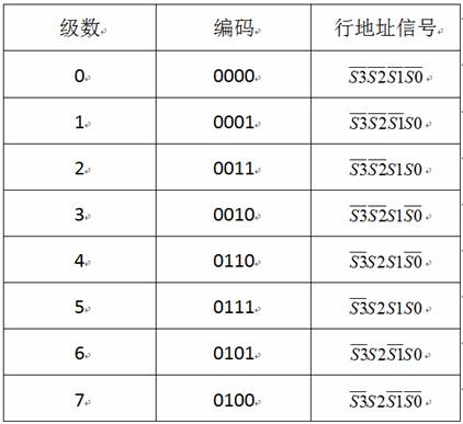
表2
这里需要说明的是图2、图3的原理图中晶体管为N型晶体管且只有16级、4个地址位。但本发明适用范围应包括N型和P型晶体管以及任意多级的情况。另外,图2、图3中的晶体管符号仅代表此处需要晶体管,并不代表此处晶体管的数量。特别的,在图3的原理图中,如果相邻行、同一列的两个晶体管满足预设条件时可以合并为一个晶体管。即相邻行、同一列的两个晶体管在满足预设条件时可以合并为一个尺寸更大、驱动能力更高的晶体管。
其中,相邻行、同一列的两个晶体管满足预设条件包括:两个晶体管的栅极短接在一起,且各自是本行译码器的最高位的晶体管,或者两个晶体管的栅极短接在一起,且紧邻前一高位的晶体管合并在一起。
当然,本发明的行译码器也可以采用P型晶体管实现,其中,P型晶体管的实现和N型晶体管的实现类似,区别点在于:编码0对应正信号,编码1对应反信号,且电压极性与N型对称。具体的,以P型晶体管实现的电路原理图如图4所示,具体编码如表3所示。

表3
同样地,P型晶体管实现的行译码器中的晶体管的合并条件与N型晶体管的合并条件相同,在此不再赘述。
进一步地,如图5b所示,为本发明以N型晶体管实现的行译码器的版图设计图。本发明通过采用前述的以晶体管串联实现的行译码器,可以使得行译码器的版图实现十分紧凑、节省面积和优化延时的效果。
具体的,如图5b所示,同一行的晶体管相互间是串联的,所以同一行的相邻晶体管的源漏极可以共用,不需要使用金属和接触孔来实现连接,该设计方式既可以节省横向的面积,又可以有效避免金属连线带来的接触电阻和负载电容对行译码器延时的影响。
其中,图5a的版图为晶体管未合并的示意图,图5b为晶体管合并后的示意图。
如图5a所示,其最左边第一列(a1)的晶体管(n11~n14),根据预设条件,由于它们的栅极短接在一起,并且各自是本行最高位的晶体管,所以,左边第一列(a1)的晶体管(n11~n14)可以合并,合并后的版图如图5b的左边第一列(a1')所示。接着考虑图6a左数第二列(a2),由于它们的栅极短接在一起,并且它们紧邻前一高位的晶体管(即左数第一列(a1)的晶体管(n11~n14))已经合并在一起,所以,根据预设条件,左数第二列(a2)的晶体管(n21~n24)也可以合并在一起,合并后的版图如图5b的左数第二列(a2')所示。接着考虑图5a左数第三列(a3),由于栅极并不全部短接在一起(如图5c所示,晶体管n31与晶体管n32的栅极短接,晶体管n33与晶体管n34的栅极短接,但是晶体管n32与晶体管n33的栅极不短接),所以这一列(a3)的4个晶体管(n31~n34)不能全部合并;但是,上半部分两个晶体管(晶体管n31与晶体管n32)和下半部分两个晶体管(晶体管n33与晶体管n34)的栅极分别短接在一起,并且它们紧邻前一高位的晶体管(即左数第二列(a2)的晶体管(n21~n24))已经合并在一起,所以根据预设条件,上半部分两个晶体管(晶体管n31与晶体管n32)和下半部分两个晶体管(晶体管n33与晶体管n34)可以分别两两合并,合并后的版图如图5b的左数第三列(a3')所示。最后考虑最低列(a4),这四个晶体管(n41~n44)只有中间两个晶体管(晶体管n42和晶体管n43)的栅极短接在一起,然而中间这两个晶体管(晶体管n42和晶体管n43)的紧邻前一高位的晶体管(晶体管n32和晶体管n33)并没有合并,所以这四个晶体管(n41~n44)不满足预设条件,不能合并,因此,最低列(a4)的四个晶体管(n41~n44)没有任何两个晶体管可以合并,所以最后行译码器合并后的版图如图5b所示。其中,图5b的电路原理图如图5c所示,在图5c中虚线框内的晶体管合并在一起。
这里需要说明的是,合并是指晶体管在版图上原属于不同行的晶体管的有源区(如图5a中的灰色区域(SS))可以融合。经过融合,可以使有源区宽度增加,即晶体管的宽度增加,可以获得更高的驱动电流(或等效来看,可以使导通电阻更低);且相互分离的有源区的边缘之间必须满足制程最小间隔要求的设计规则,而融合之后不需要考虑此规则,对掩膜版制作和光刻的要求都可以得到降低,对制程良率有很大的改善。
以下以图6a和图6b对合并后的行译码器的优势作进一步说明。
如图6a所示,考虑0001行被选中的情形。在没有合并的情况下,电流只能从本行的4个串联的TFT流过。在合并的情况下,电流向高位流动时可迅速分散到更宽的路径中(如图6b所示)。由于电阻和电流路径宽度成反比,越到高位,电阻越小,所以对使能端放电的总电阻比不合并的小,即译码速度加快。
假设,不合并情况下单个晶体管开启后的有效电阻是R,两个晶体管合并后有效电阻降为R/2。所以不合并情况下,每一行的放电总电阻为4*R;合并情况下的放电总电阻为R*(1+1/2+1/4+1/8)<2*R(等比级数)。考虑一个4096行的屏幕,需要14位地址,14个晶体管串联。不合并情况下总电阻为14*R,合并后总电阻是R*(1+1/2+1/4+1/8+ …… + 1/4096)<2*R。根据等比级数的特性可以看出合并后的总放电电阻不会随着分辨率行数的增加而等比例增加,而是存在一个上限,因此放电时间即译码时间在合并后即不受分辨率增加的影响。所以合并技术使得本发明的行译码设计可以支持高分辨率屏幕,使得译码速度基本和增加的地址线无关。
驱动模块12,其包括与使能模块11的使能信号输出端连接、用于接收使能信号输出端输出的使能信号的使能信号输入端,以及用于根据使能信号输出驱动信号的驱动信号输出端,驱动信号输出端连接与驱动模块12对应设置的行的栅线,以将驱动信号发送至对应行的栅线,选通对应行。
可选的,该驱动模块12所输出的驱动信号为脉冲信号。其中,该驱动模块12可以为脉冲发生器。
本发明实施例的方案,提供了一种支持随机寻址的GOA电路,该GOA电路允许数据不按照行的顺序写入屏幕,在屏幕大部分区域是静态图像,只有少部分区域不断变化时,只需要对该部分区域进行编程,且由于图像不变的行未选通,所以动态功耗有效降低,同时可以增加留给图像改变的每一行的时间,使得在显示尺寸和显示功率、显示刷新率之间可以实现实时、动态调整的可能。
另外,本发明的GOA电路中后级触发不依赖于前级的触发,所以当孤立一级GOA单元10出现缺陷时,其余GOA单元10的功能不会受到影响,使屏幕的良率和评级得到提升,提供了动态修理屏幕的可能。而且本发明的GOA电路不使用传统的自举结构,时钟线不需要直接驱动GOA单元10中的输出晶体管,因此,可以大大减少(N-1)级非活跃GOA单元10对动态功耗的影响。
本发明的GOA电路适用于高分辨率、大尺寸屏幕。
本发明的重置模块13有两种实施例,下面分别说明。
如图7所示,为本发明重置模块13第一实施例的电路原理图。在该实施例中,是以P型晶体管组成的译码器的任意一行与该行对应设置的重置模块13的一个实施例。
如图7所示,该重置模块13可以包括复位晶体管。
该复位晶体管的第一电极连接使能模块11的使能信号输出端,复位晶体管的第二电极接地信号(GND),复位晶体管的栅极连接外部时钟信号(CLKR)。这里需要说明的是,该外部时钟信号(CLKR)为由外部提供的额外的时钟信号。进一步地,该实施例是以P型晶体管组成的行译码器,当采用N型晶体管组成的行译码器时,其极性与P型晶体管组成的行译码器完全对称,在此不再赘述。
图7以P型晶体管做译码器、译码输出为高电平作示例。
如图7所示,当外部时钟信号(CLKR)的高脉冲到来时,复位晶体管打开,对该行译码器的输出端被下拉到低电平,该行译码器的输出端被重置为低电平。
如图8所示,为本发明重置模块13第二实施例的电路原理图。在该实施例中,是以P型晶体管组成的译码器的任意一行与该行对应设置的重置模块13的一个实施例。
如图8所示,该重置模块13包括下拉晶体管135、第一级正边沿触发器132、第一级反相器131、第二级正边沿触发器134和第二级反相器133。
第一级正边沿触发器132的正输入端(D)和第一级反相器131的输入端一并连接使能模块11的使能信号输出端,第一级正边沿触发器132的反输入端连接第一级反相器131的输出端,第一级正边沿触发器132的时钟信号输入端(CK)连接与第二级反相器133的输入端一并连接内部时钟信号(CLK);第二级正边沿触发器134的正输入端(D)连接第一级正边沿触发器132的正输出端(Q),第二级正边沿触发器134的反输入端连接第一级正边沿触发器132的反输出端,第二级正边沿触发器134的时钟信号输入端连接第二级反相器133的输出端,第二级正边沿触发器134的正输出端(Q)连接下拉晶体管135的栅极。其中,下拉晶体管135的第一电极连接使能模块11的使能信号输出端,下拉晶体管135的第二电极接地信号(GND)。
该实施例中,重置模块13不需要额外的重置时钟,其与本级锁存器共用一个内部时钟信号(CLK)及其反向信号。
如图8所示,本实施例的重置模块13是由两级级联的正边沿触发器和反相器组成的。其中,正边沿触发器是数字逻辑电路中的基本电路之一,其基本功能是:只在输入时钟的上升沿将输入端(D)的信号存储并送到输出端(Q),其他时刻不管输入端(D)如何变化,输出端(Q)的信号保持不变。基于该原理,本实施例中重置模块13的重置原理为:EN被选中、输出高电平时,在CLK上升沿锁存该高电位,并在CLK的下一个下降沿传递到下拉晶体管135的栅极(NRES端),打开下拉晶体管135,将EN重置到低电平;EN没被选中、输出为低电平时,触发器无输出,下拉晶体管135的栅极(NRES端)始终为低电平,下拉晶体管135关闭,不影响EN电位。
本发明实施例中,正边沿触发器具有多种实现形式,本发明不局限于该触发器的具体实现。以下以一个具体实施例进行说明。具体的,如图9所示,在该实施例中,所应用的正边沿触发器可以为主从触发器,其可以由两级锁存器组成。
如图9所示,第一级正边沿触发器132和第二级正边沿触发器134均包括主触发器1301、从触发器1302和主从反相器1303。
主触发器1301的输入端(S)为正边沿触发器的正输入端(D),主触发器1301的正输出端连接从触发器的输入端(S),主触发器的复位端(R)为正边沿触发器的反输入端,主触发器1301的反输出端连接从触发器1302的复位端(R);从触发器1302的正输出端(Q)为正边沿触发器的正输出端(Q),从触发器1302的反输出端为正边沿触发器的反输出端,从触发器1302的时钟信号输入端(CP)连接主从反相器1303的输出端,主从反相器1303的输入端和主触发器1301的时钟信号输入端(CP)的连接端为正边沿触发器的时钟信号输入端(CK)。
如图10所示,本发明实施例的驱动模块12可以包括:可以同时产生两种不同宽度脉冲的脉冲发生器。
本发明的脉冲发生器有两种实施例,下面分别加以说明。
图10所示是本发明的GOA电路的脉冲发生器的第一种实施例。
如图10所示,脉冲发生器的数据输入端连接时钟信号,脉冲发生器的时钟输入端连接使能模块的使能信号输出端,脉冲发生器的输出端作为驱动模块12的驱动信号输出端连接与驱动模块12对应设置的行的栅线。
脉冲发生器包括第一脉冲发生器121和第二脉冲发生器122;时钟信号包括第一时钟信号(CLKL)和第二时钟信号(CLKS)。与驱动模块12对应设置的行的栅线包括:与第一脉冲发生器121对应设置的行的第一栅线和与第二脉冲发生器122对应设置的行的第二栅线。
第一脉冲发生器121的数据输入端连接第一时钟信号(CLKL),第一脉冲发生器121的时钟输入端连接使能模块11的使能信号输出端(EN),第一脉冲发生器121的输出端(OUTL)连接与第一脉冲发生器121对应设置的行的第一栅线。
第二脉冲发生器122的数据输入端连接第二时钟信号(CLKS),第二脉冲发生器122的时钟输入端连接使能模块11的使能信号输出端(EN),第二脉冲发生器122的输出端(OUTS)连接与第二脉冲发生器122对应设置的行的第二栅线。
这里,第一脉冲发生器121的数据输入端和第二脉冲发生器122的数据输入端形成脉冲发生器的数据输入端,第一脉冲发生器121的时钟输入端和第二脉冲发生器122的时钟输入端形成脉冲发生器的时钟输入端,第一脉冲发生器121的输出端和第二脉冲发生器122的输出端形成脉冲发生器的输出端。
进一步地,如图10所示,第一脉冲发生器121包括:第一锁存器和第一缓冲放大器。
第一锁存器的第一数据输入端(S1)连接第一时钟信号(CLKL),第一锁存器的第一使能端(CP1)连接使能模块11的使能信号输出端(EN),第一锁存器的第一输出端(Q1)连接第一缓冲放大器的输入端,第一缓冲放大器的输出端连接与第一脉冲发生器121对应设置的行的第一栅线。其中,第一锁存器的第一数据输入端(S1)为第一脉冲发生器121的数据输入端,第一锁存器的第一使能端(CP1)为第一脉冲发生器121的时钟输入端,第一缓冲放大器的输出端为第一脉冲发生器121的输出端(OUTL)。
进一步地,如图10所示,第二脉冲发生器122包括:第二锁存器和第二缓冲放大器。
第二锁存器的第二数据输入端(S2)连接第二时钟信号(CLKS),第二锁存器的第二使能端(CP2)连接使能模块11的使能信号输出端(EN),第二锁存器的第二输出端(Q2)连接第二缓冲放大器的输入端,第二缓冲放大器的输出端连接与第二脉冲发生器122对应设置的行的第二栅线;
第二锁存器的第二数据输入端(S2)为第二脉冲发生器122的数据输入端,第二锁存器的第二使能端(CP2)为第二脉冲发生器的时钟输入端,第二缓冲放大器的输出端为第二脉冲发生器122的输出端(OUTS)。
其中,在图10中,每一个GOA单元10包括基于P型TFT的行译码器(使能模块11)、重置模块13、脉冲发生器(驱动模块12),其中,脉冲发生器为由第一锁存器和第一缓冲放大器组成的第一脉冲发生器121、和由第二锁存器和第二缓冲放大器组成的第二脉冲发生器122。在图10中, VDD表示输入直流高电平,S[0:N]表示输入选址信号, EN表示使能模块11的使能信号输出端,第一时钟信号(CLKL)表示输入长时钟,第二时钟信号(CLKS)表示输入短时钟,Buf表示缓冲放大器,OUTL表示第一脉冲发生器121的输出端,OUTS表示第二脉冲发生器122的输出端。
可选的,本发明实施例所采用的锁存器均为带有门控功能的锁存器,其工作原理为:
以锁存器的使能端高电平有效的锁存器为例:
当锁存器的使能端电位为低电平时,锁存器的输出端保持不变,锁存器的数据输入端的信号不影响其输出端。
当锁存器的使能端电位为高电平时,锁存器的输出端的二进制信号随着锁存器的数据输入端的输入电位变化。可以理解地,锁存器有多种实施方案,本发明不局限于锁存器的某一种具体实施方案。本发明通过在每个GOA单元10中采用锁存器可以产生以下优势:利用锁存原理,可以有效抑制电路内部交流信号或毛刺信号偶合到输出端,且锁存器具有波形重建功能,即使外部时钟小型因为RC延时产生变形,经过锁存器重建以后,也能输出高质量方波脉冲。
其中,最常用的锁存器为SR型锁存器。此处对SR型锁存器的两种典型的实施例展开说明。
如图11所示,在一个具体的实施例中,第一锁存器包括:锁存反相器1210、第一与门1211、第二与门1212、第一或非门1213和第二或非门1214。
锁存反相器1210的输入端与第一与门1211的第一输入端一并连接内部时钟信号(CLK),锁存反相器1210的输出端连接第二与门1212的第二输入端,第一与门1211的第二输入端和第二与门1212的第一输入端一并连接使能模块11的使能信号输出端(EN);第一与门1211的输出端连接第一或非门1213的第一输入端,第一或非门1213的第二输入端连接第二或非门1214的输出端,第一或非门1213的输出端连接第二或非门1214的第一输入端,第一或非门1213的输出端还连接缓冲放大电路122的输入端;第二或非门1214的第二输入端连接第二与门1212的输出端。
其中,第一与门1211的第一输入端和锁存反相器1210的输入端的连接端为第一锁存器的第一数据输入端,第一与门1211的第二输入端和第二与门1212的第一输入端的连接端为第一锁存器的第一使能端,第一或非门1213的输出端为第一锁存器的第一输出端。
同样地,第二锁存器也可以采用与第一锁存器相同的结构,其具体结构组成和连接关系如前述,在此不再赘述。且同样地,第一与门1211的第一输入端和锁存反相器1210的输入端的连接端为第二锁存器的第二数据输入端,第一与门1211的第二输入端和第二与门1212的第一输入端的连接端为第二锁存器的第二使能端,第一或非门1213的输出端为第二锁存器的第二输出端。
进一步地,如图12所示,在锁存器的第二种具体的实施例中,第一锁存器可以包括:第一非门1201、第二非门1202、第三非门1203、第一晶体管1204、第二晶体管1205和第三晶体管1206。这里,第一晶体管和第三晶体管是N型晶体管,第二晶体管是P型晶体管。
第一非门1201的输入端连接第三晶体管1206的第二电极,第一非门1201的输出端连接第一晶体管1204的第一电极,第一晶体管1204的第二电极分别连接第三非门1203的输入端和第二非门1202的输出端,第一晶体管1204的第三电极分别连接第二晶体管1205的第三电极和第三晶体管1206的第三电极;第三非门1203的输出端连接第二晶体管1205的第一电极,第二晶体管1205的第二电极分别连接第二非门1202的输入端和第三晶体管1206的第一电极。
其中,第一非门1201的输入端和第三晶体管1206的第二电极为第一锁存器的第一数据输入端;第三非门1023的输出端为第一锁存器的第一输出端;第一晶体管1204的第三电极、第二晶体管1205的第三电极和第三晶体管1206的第三电极为第一锁存器的第一使能端。
该实施例中,第二锁存器也可以采用与第一锁存器相同的结构,其具体的结构组成和连接关系如前述,在此不再赘述。同样地,第一非门1201的输入端和第三晶体管1206的第二电极也可以作为第二锁存器的第一数据输入端;第三非门1203的输出端也可以作为第二锁存器的第二输出端;第一晶体管1204的第三电极、第二晶体管1205的第三电极和第三晶体管1206的第三电极也可以作为第二锁存器的第二使能端。同样地,这里的第一晶体管和第三晶体管是N型晶体管,第二晶体管是P型晶体管。
如图13所示,为本发明实施例提供的缓冲放大器的电路原理图。
本发明实施例提供的第一缓冲放大器和第二缓冲放大器均可以由两级反相器或者多级级联的反相器组成。
若第一缓冲放大器有n级,n为大于或等于2的偶数,则第一锁存器的第一数据输入端(S1)连接第一时钟信号(CLKL),第一锁存器的第一使能端(CP1)连接使能模块11的使能信号输出端(EN),第一锁存器的第一输出端(Q1)连接第1级反相器的输入端,第n级反相器的输出端作为第一缓冲放大器的输出端(OUTL)连接与第一脉冲发生器121对应设置的行的第一栅线。
若第二缓冲放大器有n级,n为大于或等于2的偶数,则第二锁存器的第二数据输入端(S2)连接第二时钟信号(CLKS),第二锁存器的第二使能端(CP2)连接使能模块11的使能信号输出端(EN),第二锁存器的第二输出端(Q2)连接第1级反相器的输入端,第n级反相器的输出端作为第二缓冲放大器的输出端(OUTL)连接与第二脉冲发生器122对应设置的行的第二栅线。
进一步地,本发明实施例中多级级联的反相器中所采用的反相器均可以由晶体管组成。
具体的,如图13所示,每一个反相器均可以包括:P型晶体管和N型晶体管。
具体的,P型晶体管的第一电极连接恒压高电位(VGH),P型晶体管的第二电极连接N型晶体管的第一电极,N型晶体管的第二电极连接恒压低电位(VGL),P型晶体管的栅极和N型晶体管的栅极连接,P型晶体管的第二电极和N型晶体管的第一电极连接。
其中,P型晶体管的栅极和N型晶体管的栅极为反相器的输入端,P型晶体管的第二电极和N型晶体管的第一电极为反相器的输出端。
这里需要说明的是,本发明实施例中,每一个GOA单元10中的P型晶体管是低温多晶硅、无定型硅、或者是由碳、硅、锗三种元素按任意比例混合的材料制作沟道的薄膜晶体管。每一个GOA单元10中的N型晶体管是基于金属氧化物制作沟道的薄膜晶体管。而且,本发明实施例为基于互补极性的晶体管的GOA电路,即在面板上可以同时存在N型和P型晶体管的情况。
参考图14,为采用的脉冲发生器第一实施例(即图10的电路图)的工作时序图。
如图14所示,输入行地址信号激活译码器,EN抬升,EN输出为高期间,第一锁存器和第二锁存器开启,输出第一脉冲信号和第二脉冲信号,其中,第一脉冲信号为长脉冲信号,第二脉冲信号为短脉冲信号。重置模块13激活,EN下降,第一锁存器和第二锁存器关闭,不再输出脉冲。
图15,为本发明中GOA电路采用的脉冲发生器的第二实施例的电路原理图。
如图15所示,在该实施例中,第一脉冲发生器121包括:第一级与门和第一缓冲放大器。
第一级与门的第一输入端连接第一时钟信号(CLKL),第一与门的第二输入端连接使能模块11的使能信号输出端,第一与门的输出端连接第一缓冲放大器的输入端,第一缓冲放大器的输出端连接与第一脉冲发生器121对应设置的行的第一栅线;第一级与门的第一输入端为第一脉冲发生器121的数据输入端,第一级与门的第二输入端为第一脉冲发生器121的时钟输入端,第一缓冲放大器的输出端为第一脉冲发生器121的输出端(OUTL)。
第二脉冲发生器122包括:第二级与门和第二缓冲放大器。
第二级与门的第一输入端连接第二时钟信号(CLKS),第二级与门的第二输入端连接使能模块11的使能信号输出端,第二级与门的输出端连接第二缓冲放大器的输入端,第二缓冲放大器的输出端连接与第二脉冲发生器122对应设置的行的第二栅线;第二级与门的第一输入端为第二脉冲发生器122的数据输入端,第二级与门的第二输入端为第二脉冲发生器122的时钟输入端,第二缓冲放大器的输出端为第二脉冲发生器122的输出端(OUTS)。
如图15所示,该实施例中,每一个GOA单元10包括:基于P型TFT的行译码器(使能模块11)、重置模块13、脉冲发生器(驱动模块12),其中,脉冲发生器为由第一级与门和第一缓冲放大器组成的第一脉冲发生器121、由第二级与门和第二缓冲放大器组成的第二脉冲发生器122。在具体实施中,与门可以用与非门+反相器代替,其中反相器并入缓冲放大器中;或者,在其他一些实施例中,与门还可以替换为反相器+或非门。该实施例以简单的逻辑门电路代替第一实施例中使用的锁存器。
参考图16,为采用图15的脉冲发生器的工作时序图。
如图16所示,输入选址信号激活译码器,EN抬升;EN输出为高电平期间,第一级与门和第二级与门打开,输出第一脉冲信号和第二脉冲信号;重置模块13激活,EN下降,第一级与门和第二级与门关闭,不再输出脉冲。
由前文描述可知,本发明实施例的GOA电路的各个组件(重置模块13、锁存器、脉冲发生器)存在多种实施例,将各个组件的不同实施例排列组合,可以得到多种可能的电路实施方案。而且不同的方案可以在面积、功耗、可靠性、抗干扰能力和波形质量各方面取得不同的折中。
以下列举三个具体的完整实施方案,并提供对应的级联方案和时序图,同时提供仿真验证结果和工作时序图的比较。
为了简化电路原理图,本发明实施例提供的原理图只以四位地址为例(此时译码器只包含四个晶体管)。仿真以8位地址为例(地址总线以S[0:N]标示)。需要说明的是,在实际实施中,可以扩展到任意多位。
参考图17,本发明提供的第一种GOA电路的电路原理图。
在该实施例中,重置模块13采用第二实施例,脉冲发生器采用第一实施例。其单级工作时序图和仿真时序图如图18所示。由图18中可以看出,其理论工作时序与仿真时序的验证结果相当。
参考图19,为本发明提供的第二种GOA电路的电路原理图。
在该实施例中,重置模块13采用第二实施例,脉冲发生器采用第二实施例。如前述,本实施例的脉冲发生器采用第二实施例时,可以用非门和或非门代替最初原理图中的与门。可以理解地,在一些实施例中,在某些工艺制程中,或非门可能取得比与门、与非门更好的电路性能,或者具有更小的面积。其单级工作时序图和仿真时序图如图20所示。由图20可以看出,本实施例关键节点的时序图和图17的第一种GOA电路的时序图一致,且本实施例与图17的实施例相比,具有占用面积小、使用晶体管数少。
参考图21,为本发明提供的第一种GOA电路、第二种GOA电路的级联方式示意图。
其中,图22给出了采用图17的第一种GOA电路级联的全局时序,而图23为采用图17的第一种GOA电路级联的全局时序的仿真图。对比图22和图23可以看出,采用图17的第一种GOA电路级联的全局工作时序与仿真时序相当。
参考图24本发明提供采用图19所示第二种GOA电路级联的全局时序图,图25为其仿真时序图。由图24和图25可以看出,该种电路的全局输入、输出波形无论在原理图还是在仿真图中都与图22和图23的几乎相同。
参考图26,为本发明提供的第三种GOA电路的电路原理图。
在该实施例中,重置模块13采用第一实施例的电路,脉冲发生器采用第二实施例的电路。本实施例与图20的第二种GOA电路相比,使用晶体管更少、面积更小。
参考图27,为图26的单级时序图。这里,仅显示全局使用最少时钟数目的情况。其中仿真时序图如图28所示,可以看出,其工作时序与仿真时序结果相当。
参考图29,为本发明提供的第三种GOA电路的级联方式示意图。其全局时序图和仿真时序图分别如图30和图31所示。由图30和图31对比可以看出,其工作时序与仿真时序结果相当。
本发明提供了一种支持随机寻址的GOA电路,该GOA电路允许数据不按照行的顺序写入屏幕,在屏幕大部分区域是静态图像,只有少部分区域不断变化时,只需要对该部分区域进行编程,且由于图像不变的行未选通,所以动态功耗有效降低,同时可以增加留给图像改变的每一行的时间,使得在显示尺寸和显示功率、显示刷新率之间可以实现实时、动态调整的可能。
本发明的GOA电路中后级触发不依赖于前级的触发,所以当孤立一级GOA单元出现缺陷时,其余GOA单元的功能不会受到影响,使屏幕的和评级得到提升,提供了动态修理屏幕的可能。而且本发明的GOA电路不使用传统的自举结构,在某些实施例中时钟线不需要直接驱动GOA单元中的输出晶体管,因此,可以大大减少(N-1)级非活跃GOA单元对动态功耗的影响。本发明的GOA电路适用于高分辨率、大尺寸屏幕。
另外,本发明的GOA电路可以使得面板显示电路中的像素电路具有如下优势:高驱动P型晶体管提供充足发光电流、节省像素面积;低漏电流N型晶体管保持电压数据完整,允许可变刷新率;输入驱动波形简单,对存储电容的要求不高发光电流完全由驱动晶体管决定,对OLED老化不敏感;具有内部补偿功能,可以对由于工艺波动、电学压力、材料老化或者机械应力造成的高驱动P型晶体管的阈值电压的临时或永久波动进行自动补偿,从而延长屏幕的使用寿命、提高屏幕的均一性。
进一步地,本发明实施例提供的GOA电路通过引入前述实施例的脉冲发生器,可以产生用于驱动各行像素的长、短脉冲信号,可以与像素电路直接配合使用。相比已有的GOA电路只能提供一种宽度的扫描脉冲,本发明实施例提供的GOA电路可以满足具有内部补偿功能的像素电路同时需要两种宽度的扫描脉冲的需求,且不会增加边框面积和功耗。
如图32所示,本发明还提供了一种与本发明的GOA配合工作的具有内部补偿效果的像素电路。
其中,图32为本发明提供的具有内部补偿效果的像素电路的第一实施例的电路原理图。
如图32所示,该像素电路包括:第一晶体管T1、第二晶体管T2、第三晶体管T3、第四晶体管T4、第五晶体管T5、电容C
s、节点(nst)以及发光单元(OLED)。
其中,第一晶体管T1的第二电极接入数据信号(Data),第一晶体管T1的第一电极连接第四晶体管T4的第二电极和第二晶体管T2的第一电极,第一晶体管T1的第三电极和第五晶体管的第三电极连接驱动模块12的第二输出端;第四晶体管T4的第一电极连接高电平(Vdd),第四晶体管的第三电极和第三晶体管T3的第三电极连接驱动模块12的第一输出端,第二晶体管T2的第二电极和第三晶体管T3的第二电极一并连接第五晶体管T5的第一电极,第五晶体管T5的第二电极连接发光单元(OLED)的正极,发光单元(OLED)的负极连接低电平(Vss);第三晶体管T3的第一电极依次通过连接节点(nst)和电容C
s连接高电平(Vdd),节点(nst)还连接第二晶体管T2的第三电极。
第四晶体管T4的第三电极和第三晶体管T3的第三电极为与第一脉冲发生器121对应设置的行的第一栅线;第一晶体管T1的第三电极和第五晶体管T5的第三电极为与第二脉冲发生器122对应设置的行的第二栅线。第一脉冲发生器121的第一输出端为驱动模块12的第一输出端,第二脉冲发生器122的第二输出端为驱动模块12的第二输出端。
如图10或者图15所示,第一脉冲发生器121的第一输出端输出的第一脉冲信号(En)为长脉冲信号,第二脉冲发生器122的第二输出端输出的第二脉冲信号(Gn)为短脉冲信号,即第一脉冲信号(En)的高电平脉冲宽度大于第二脉冲信号(Gn)的高电平脉冲宽度。
进一步地,上述由5个晶体管和1个电容(即5T1C)实现的像素电路的工作时序如图33所示,结合图33对该实施例的电路的工作过程进行说明:
第一阶段:当第一脉冲发生器121输出的第一脉冲信号(En)为高电平,第二脉冲发生器122输出的第二脉冲信号(Gn)为低电平时,第一晶体管T1和第四晶体管T4关闭,第三晶体管T3和第五晶体管T5打开,节点(nst)通过第三晶体管T3、第五晶体管T5、发光单元(OLED)放电到低电平(Vss)。
第二阶段:第一晶体管T1打开,数据信号(Data)通过第二晶体管T2、第三晶体管T3对节点(nst)充电,节点(nst)电压终止于Vdata-Vt,实现对第二晶体管T2阈值电压的采样。其中,Vt为第二晶体管的阈值电压。
第三阶段:第四晶体管T4、第二晶体管T2、第五晶体管T5打开,第一晶体管T1、第三晶体管T3关闭。发光单元(OLED)发光,第二晶体管T2(Vgs)电压为(Vdd-Vdata+Vt),故取得Vt的补偿效果。
或者,在另一个实施例中,如图34所示,与本发明的GOA电路配合工作的像素电路包括:第一晶体管T1、第二晶体管T2、第三晶体管T3、第四晶体管T4、电容C
s、节点(nst)以及发光单元(OLED)。
第一晶体管T1的第二电极接入数据信号(Data),第一晶体管T1的第一电极连接第四晶体管T4的第二电极和第二晶体管T2的第一电极,第一晶体管T1的第三电极连接第二脉冲发生器122的第二输出端;第四晶体管T4第一电极连接高电平(Vdd),第四晶体管的第三电极和第三晶体管T3的第三电极连接第一脉冲发生器121的第一输出端,第二晶体管T2的第二电极和第三晶体管T3的第二电极一并连接发光单元(OLED)的正极,发光单元(OLED)的负极连接低电平(Vss);第三晶体管T3的第一电极依次通过连接节点(nst)和电容C
s连接高电平(Vdd),节点(nst)还连接第二晶体管T2的第三电极。
第四晶体管T4的第三电极和第三晶体管T3的第三电极为与第一脉冲发生器121对应设置的行的第一栅线;第一晶体管T1的第三电极为与第二脉冲发生器122对应设置的行的第二栅线。
上述像素电路的第二实施例中,像素电路由4个晶体管和1个电容(即4T1C)实现。其具体工作时序如图33所示,其中,该实施例的电路工作过程与前述实施例相同,在此不再赘述。
进一步地,本发明实施例所提供的像素电路中所采用的第一晶体管T1和第三晶体管T3为N型晶体管,第二晶体管T2、第四晶体管T4、第五晶体管T5为P型晶体管。每一个像素电路中的P型晶体管是低温多晶硅、无定型硅、或者是由碳、硅、锗三种元素按任意比例混合的材料制作沟道的薄膜晶体管。每一个像素电路中的N型晶体管是基于金属氧化物制作沟道的薄膜晶体管。
本发明的显示装置中的像素电路具有如下优势:高驱动P型晶体管提供充足发光电流、节省像素面积;低漏电流N型晶体管保持电压数据完整,允许可变刷新率;输入驱动波形简单,对存储电容的要求不高发光电流完全由驱动晶体管决定,对OLED老化不敏感;具有内部补偿功能,可以对由于工艺波动、电学压力、材料老化或者机械应力造成的高驱动P型晶体管的阈值电压的临时或永久波动进行自动补偿,从而延长屏幕的使用寿命、提高屏幕的均一性。
进一步地,本发明还提供了一种显示装置,该显示装置包括前述实施例的GOA电路和具有内部补偿效果的像素电路。其中,该显示装置包括但不限于LTPS显示装置、AMOLED显示装置。
参考图35,为本发明实施例提供的一种显示器的驱动方法的流程示意图。如图35所示,该显示器的驱动方法可以包括以下步骤:
步骤S1、输入寻址信号至显示器的GOA电路的各行译码器。
步骤S2、选通与所述寻址信号对应的行译码器。
步骤S3、通过选通的行译码器输出使能信号至所述GOA电路中的脉冲发生器。
步骤S4、通过所述脉冲发生器产生脉冲信号驱动对应行的像素工作。
本发明实施例中,该显示器的驱动方法中的GOA电路可以为前述实施例所提供的GOA电路。
进一步地,本发明实施例中,脉冲发生器分别产生短脉冲信号和长脉冲信号,以分别驱动不同行的像素工作,即本发明实施例的GOA电路可以同时产生两种宽度的脉冲信号。可以理解地,这里的短脉冲信号即为前述的第二脉冲信号,长脉冲信号即为前述的第一脉冲信号。
进一步地,脉冲发生器还接收长时钟信号和短时钟信号,并分别根据长时钟信号和短时钟信号产生长脉冲信号和短脉冲信号。可以理解地,这里的长时钟信号为前述的第一时钟信号(CLKL),短时钟信号为前述的第二时钟信号(CLKS)。
本发明实施例中,脉冲发生器可以包括第一脉冲发生器和第二脉冲发生器,其中,长时钟信号输入第一脉冲发生器的数据输入端,短时钟信号输入第二脉冲发生器的数据输入端,使能信号输入第一脉冲发生器的时钟输入端和第二脉冲发生器的时钟输入端。
进一步地,本发明实施例的显示器的驱动方法还包括:对开启的行译码器输出的使能信号复位。其中,对开启的行译码器输出的使能信号复位可以通过复位电路执行。
进一步地,本发明实施例的显示器的驱动方法还包括:输入长时钟信号或者短时钟信号至复位电路,该复位电路根据长时钟信号或者短时钟信号对使能信号进行复位。
以上实施例只为说明本发明的技术构思及特点,其目的在于让熟悉此项技术的人士能够了解本发明的内容并据此实施,并不能限制本发明的保护范围。凡跟本发明权利要求范围所做的均等变化与修饰,均应属于本发明权利要求的涵盖范围。
应当理解的是,对本领域普通技术人员来说,可以根据上述说明加以改进或变换,而所有这些改进和变换都应属于本发明所附权利要求的保护范围。
Claims (36)
- 一种GOA电路,其特征在于,包括多个相互独立的GOA单元,每一个所述GOA单元包括一个使能模块以及与所述使能模块对应设置的驱动模块;所述使能模块包括用于接收行地址信号的地址输入端,以及用于根据所述行地址信号输出使能信号的使能信号输出端;所述驱动模块包括用于接收所述使能信号输出端输出的使能信号的使能信号输入端,以及用于根据所述使能信号输出脉冲宽度不同的驱动信号的驱动信号输出端,所述驱动信号输出端连接与所述驱动模块对应设置的行的栅线,以将所述驱动信号发送至所述对应行的栅线,选通所述对应行。
- 根据权利要求1所述的GOA电路,其特征在于,所述使能模块为基于二进制编码的行译码器或者基于格雷码编码的行译码器。
- 根据权利要求2所述的GOA电路,其特征在于,所述每一行译码器包括多个串联的晶体管,且相邻行、同一列的两个晶体管在满足预设条件时合并为一个晶体管。
- 根据权利要求3所述的GOA电路,其特征在于,所述相邻行、同一列的两个晶体管满足预设条件包括:两个晶体管的栅极短接在一起,且各自是本行译码器的最高位的晶体管,或者两个晶体管的栅极短接在一起,且紧邻前一高位的晶体管合并在一起。
- 根据权利要求1所述的GOA电路,其特征在于,每一个所述GOA单元还包括与所述使能模块的使能信号输出端连接、用于在所述驱动模块输出驱动信号并将所述对应行选通后、将所述使能模块重置的重置模块。
- 根据权利要求5所述的GOA电路,其特征在于,所述重置模块包括复位晶体管;所述复位晶体管的第一电极连接所述使能模块的使能信号输出端,所述复位晶体管的第二电极接地信号,所述复位晶体管的栅极连接外部时钟信号。
- 根据权利要求5所述的GOA电路,其特征在于,所述重置模块包括下拉晶体管、第一级正边沿触发器、第一级反相器、第二级正边沿触发器和第二级反相器;所述第一级正边沿触发器的正输入端和所述第一级反相器的输入端一并连接所述使能模块的使能信号输出端,所述第一级正边沿触发器的反输入端连接所述第一级反相器的输出端,所述第一级正边沿触发器的时钟信号输入端与所述第二级反相器的输入端一并连接内部时钟信号;所述第二级正边沿触发器的正输入端连接所述第一级正边沿触发器的正输出端,所述第二级正边沿触发器的反输入端连接所述第一级正边沿触发器的反输出端,所述第二级正边沿触发器的时钟信号输入端连接所述第二级反相器的输出端,所述第二级正边沿触发器的正输出端连接所述下拉晶体管的栅极;所述下拉晶体管的第一电极连接所述使能模块的使能信号输出端,所述下拉晶体管的第二电极接地信号。
- 根据权利要求7所述的GOA电路,其特征在于,所述第一级正边沿触发器和所述第二级正边沿触发器均包括主触发器、从触发器和主从反相器;所述主触发器的输入端为正边沿触发器的正输入端,所述主触发器的正输出端连接所述从触发器的输入端,所述主触发器的复位端为正边沿触发器的反输入端,所述主触发器的反输出端连接所述从触发器的复位端;所述从触发器的正输出端为正边沿触发器的正输出端,所述从触发器的反输出端为正边沿触发器的反输出端,所述从触发器的时钟信号输入端连接所述主从反相器的输出端,所述主从反相器的输入端和所述主触发器的时钟信号输入端为正边沿触发器的时钟信号输入端。
- 根据权利要求1所述的GOA电路,其特征在于,所述驱动模块包括:脉冲发生器;所述脉冲发生器的数据输入端连接时钟信号,所述脉冲发生器的时钟输入端连接所述使能模块的使能信号输出端,所述脉冲发生器的输出端作为所述驱动模块的驱动信号输出端连接与所述驱动模块对应设置的行的栅线。
- 根据权利要求9所述的GOA电路,其特征在于,所述脉冲发生器包括:第一脉冲发生器和第二脉冲发生器;所述时钟信号包括:第一时钟信号和第二时钟信号;所述与所述驱动模块对应设置的行的栅线包括:与所述第一脉冲发生器对应设置的行的第一栅线和与所述第二脉冲发生器对应设置的行的第二栅线;所述第一脉冲发生器的数据输入端连接所述第一时钟信号,所述第一脉冲发生器的时钟输入端连接所述使能模块的使能信号输出端,所述第一脉冲发生器的输出端连接与所述第一脉冲发生器对应设置的行的第一栅线;所述第二脉冲发生器的数据输入端连接所述第二时钟信号,所述第二脉冲发生器的时钟输入端连接所述使能模块的使能信号输出端,所述第二脉冲发生器的输出端连接与所述第二脉冲发生器对应设置的行的第二栅线。
- 根据权利要求10所述的GOA电路,其特征在于,所述第一脉冲发生器包括:第一锁存器和第一缓冲放大器;所述第一锁存器的第一数据输入端连接所述第一时钟信号,所述第一锁存器的第一使能端连接所述使能模块的使能信号输出端,所述第一锁存器的第一输出端连接所述第一缓冲放大器的输入端,所述第一缓冲放大器的输出端连接与所述第一脉冲发生器对应设置的行的第一栅线;所述第一锁存器的第一数据输入端为所述第一脉冲发生器的数据输入端,所述第一锁存器的第一使能端为所述第一脉冲发生器的时钟输入端,所述第一缓冲放大器的输出端为所述第一脉冲发生器的输出端。
- 根据权利要求11所述的GOA电路,其特征在于,所述第二脉冲发生器包括:第二锁存器和第二缓冲放大器;所述第二锁存器的第二数据输入端连接所述第二时钟信号,所述第二锁存器的第二使能端连接所述使能模块的使能信号输出端,所述第二锁存器的第二输出端连接所述第二缓冲放大器的输入端,所述第二缓冲放大器的输出端连接与所述第二脉冲发生器对应设置的行的栅线;所述第二锁存器的第二数据输入端为所述第二脉冲发生器的数据输入端,所述第二锁存器的第二使能端为所述第二脉冲发生器的时钟输入端,所述第二缓冲放大器的输出端为所述第二脉冲发生器的输出端。
- 根据权利要求12所述的GOA电路,其特征在于,所述第一锁存器和第二锁存器均包括:锁存反相器、第一与门、第二与门、第一或非门和第二或非门;所述锁存反相器的输入端与所述第一与门的第一输入端连接,所述锁存反相器的输出端连接所述第二与门的第二输入端,所述第一与门的第二输入端和所述第二与门的第一输入端连接;所述第一与门的输出端连接所述第一或非门的第一输入端,所述第一或非门的第二输入端连接所述第二或非门的输出端,所述第一或非门的输出端连接所述第二或非门的第一输入端;所述第二或非门的第二输入端连接所述第二与门的输出端;所述第一锁存器的第一数据输入端和第二锁存器的第二数据输入端均为所述第一与门的第一输入端和所述锁存反相器的输入端的连接端;所述第一锁存器的第一输出端和第二锁存器的第二输出端均为所述第一或非门的输出端;所述第一锁存器的第一使能端和第二锁存器的第二使能端均为所述第一与门的第二输入端和所述第二与门的第一输入端的连接端。
- 根据权利要求13所述的GOA电路,其特征在于,所述第一锁存器和第二锁存器均包括:第一非门、第二非门、第三非门、第一晶体管、第二晶体管和第三晶体管;所述第一晶体管和第三晶体管是N型晶体管,所述第二晶体管是P型晶体管;所述第一非门的输入端连接所述第三晶体管的第二电极,所述第一非门的输出端连接所述第一晶体管的第一电极,所述第一晶体管的第二电极分别连接所述第三非门的输入端和所述第二非门的输出端,所述第一晶体管的第三电极分别连接所述第二晶体管的第三电极和所述第三晶体管的第三电极;所述第三非门的输出端连接所述第二晶体管的第一电极,所述第二晶体管的第二电极分别连接所述第二非门的输入端和所述第三晶体管的第一电极;所述第一锁存器的第一数据输入端和第二锁存器的第二数据输入端均为所述第一非门的输入端和所述第三晶体管的第二电极的连接端;所述第一锁存器的第一输出端和第二锁存器的第二输出端均为所述第三非门的输出端;所述第一锁存器的使能端和第二锁存器的使能端均为所述第一晶体管的第三电极、所述第二晶体管的第三电极和所述第三晶体管的第三电极的连接端。
- 根据权利要求10所述的GOA电路,其特征在于,所述第一脉冲发生器包括:第一级与门和第一缓冲放大器;所述第一级与门的第一输入端连接所述第一时钟信号,所述第一级与门的第二输入端连接所述使能模块的使能信号输出端,所述第一级与门的输出端连接所述第一缓冲放大器的输入端,所述第一缓冲放大器的输出端连接与所述第一脉冲发生器对应设置的行的第一栅线;所述第一级与门的第一输入端为所述第一脉冲发生器的数据输入端,所述第一级与门的第二输入端为所述第一脉冲发生器的使能输入端,所述第一缓冲放大器的输出端为所述第一脉冲发生器的输出端。
- 根据权利要求15所述的GOA电路,其特征在于,所述第二脉冲发生器包括:第二级与门和第二缓冲放大器;所述第二级与门的第一输入端连接所述第二时钟信号,所述第二级与门的第二输入端连接所述使能模块的使能信号输出端,所述第二级与门的输出端连接所述第二缓冲放大器的输入端,所述第二缓冲放大器的输出端连接与所述第二脉冲发生器对应设置的行的第二栅线;所述第二级与门的第一输入端为所述第二脉冲发生器的数据输入端,所述第二级与门的第二输入端为所述第二脉冲发生器的使能输入端,所述第二缓冲放大器的输出端为所述第二脉冲发生器的输出端。
- 根据权利要求16所述的GOA电路,其特征在于,所述第一缓冲放大器和所述第二缓冲放大器均包括:n级级联的反相器,其中,n为大于或等于2的偶数;所述第一缓冲放大器的输入端和所述第二缓冲放大器的输入端均为第1级反相器的输入端,所述第一缓冲放大器的输出端和所述第二缓冲放大器的输出端均为第n级反相器的输出端。
- 根据权利要求17所述的GOA电路,其特征在于,所述n级级联的反相器中的每一个反相器均包括: P型晶体管和N型晶体管;所述P型晶体管的第一电极连接恒压高电位,所述P型晶体管的第二电极连接所述N型晶体管的第一电极,所述N型晶体管的第二电极连接恒压低电位,所述P型晶体管的栅极和所述N型晶体管的栅极连接,所述P型晶体管的第二电极和所述N型晶体管的第一电极连接;其中,所述P型晶体管的栅极和所述N型晶体管的栅极为反相器的输入端,所述P型晶体管的第二电极和所述N型晶体管的第一电极为反相器的输出端。
- 根据权利要求1所述的GOA电路,其特征在于,每一个所述GOA单元中的P型晶体管是低温多晶硅、无定型硅、或者是由碳、硅、锗三种元素按任意比例混合的材料制作沟道的薄膜晶体管。
- 根据权利要求1所述的GOA电路,其特征在于,每一个所述GOA单元中的N型晶体管是基于金属氧化物制作沟道的薄膜晶体管。
- 一种具有内部补偿效果的像素电路,与权利要求1-20任一项所述的GOA电路配合工作,其特征在于,包括:第一晶体管T1、第二晶体管T2、第三晶体管T3、第四晶体管T4、第五晶体管T5、电容C s、节点以及发光单元;所述第一晶体管T1的第二电极接入数据信号,所述第一晶体管T1的第一电极连接所述第四晶体管T4的第二电极和所述第二晶体管T2的第一电极,所述第一晶体管T1的第三电极和所述第五晶体管T5的第三电极连接所述GOA电路中的驱动模块的第二输出端;所述第四晶体管T4的第一电极连接高电平,所述第四晶体管T4的第三电极和所述第三晶体管T3的第三电极连接所述GOA电路中的驱动模块的第一输出端,所述第二晶体管T2的第二电极和所述第三晶体管T3的第二电极一并连接所述第五晶体管T5的第一电极,所述第五晶体管T5的第二电极连接所述发光单元的正极,所述发光单元的负极连接低电平;所述第三晶体管T3的第一电极依次通过连接节点和所述电容C s连接高电平,所述节点还连接所述第二晶体管T2的第三电极。
- 根据权利要求21所述的具有内部补偿效果的像素电路,其特征在于,所述第一晶体管T1和第三晶体管T3为N型晶体管,所述第二晶体管T2、所述第四晶体管T4和所述第五晶体管T5为P型晶体管。
- 根据权利要求21所述的具有内部补偿效果的像素电路,其特征在于,每一个所述像素电路中的P型晶体管是低温多晶硅、无定型硅、或者是由碳、硅、锗三种元素按任意比例混合的材料制作沟道的薄膜晶体管。
- 根据权利要求21所述的具有内部补偿效果的像素电路,其特征在于,每一个所述像素电路中的N型晶体管是基于金属氧化物制作沟道的薄膜晶体管。
- 一种具有内部补偿效果的像素电路,与权利要求1-20任一项所述的GOA电路配合工作,其特征在于,包括:第一晶体管T1、第二晶体管T2、第三晶体管T3、第四晶体管T4、电容C s、节点以及发光单元;所述第一晶体管T1的第二电极接入数据信号,所述第一晶体管T1的第一电极连接所述第四晶体管T4的第二电极和所述第二晶体管T2的第一电极,所述第一晶体管T1的第三电极连接所述GOA电路中的驱动模块的第二输出端;所述第四晶体管T4第一电极连接高电平,所述第四晶体管的第三电极和所述第三晶体管T3的第三电极连接所述GOA电路中的驱动模块的第一输出端,所述第二晶体管T2的第二电极和所述第三晶体管T3的第二电极一并连接所述发光单元的正极,所述发光单元的负极连接低电平;所述第三晶体管T3的第一电极依次通过连接节点和所述电容C s连接高电平,所述节点还连接所述第二晶体管T2的第三电极。
- 根据权利要求25所述的具有内部补偿效果的像素电路,其特征在于,所述第一晶体管T1和第三晶体管T3为N型晶体管,所述第二晶体管T2和所述第四晶体管T4为P型晶体管。
- 根据权利要求25所述的具有内部补偿效果的像素电路,其特征在于,每一个所述像素电路中的P型晶体管是低温多晶硅、无定型硅、或者是由碳、硅、锗三种元素按任意比例混合的材料制作沟道的薄膜晶体管。
- 根据权利要求27所述的具有内部补偿效果的像素电路,其特征在于,每一个所述像素电路中的N型晶体管是基于金属氧化物制作沟道的薄膜晶体管。
- 一种显示装置,其特征在于,包括权利要求1-20任一项所述的GOA电路和权利要求21或25所述的具有内部补偿效果的像素电路。
- 一种显示器的驱动方法,其特征在于,包括:输入寻址信号至显示器的GOA电路的各行译码器;选通与所述寻址信号对应的行译码器;通过选通的行译码器输出使能信号至所述GOA电路中的脉冲发生器;通过所述脉冲发生器产生脉冲信号驱动对应行的像素工作。
- 根据权利要求30所述的显示器的驱动方法,其特征在于,所述脉冲发生器分别产生短脉冲信号和长脉冲信号,以分别驱动不同行的像素工作。
- 根据权利要求31所述的显示器的驱动方法,其特征在于,所述脉冲发生器接收长时钟信号及短时钟信号而分别产生所述长脉冲信号和短脉冲信号。
- 根据权利要求32所述的显示器的驱动方法,其特征在于,所述脉冲发生器包括第一脉冲发生器和第二脉冲发生器;所述长时钟信号输入所述第一脉冲发生器的数据输入端,所述短时钟信号输入所述第二脉冲发生器的数据输入端,使能信号输入所述第一脉冲发生器的时钟输入端和所述第二脉冲发生器的时钟输入端。
- 根据权利要求30所述的显示器的驱动方法,其特征在于,还包括:对开启的行译码器输出的使能信号复位。
- 根据权利要求34所述的显示器的驱动方法,其特征在于,所述对开启的行译码器复位通过复位电路执行。
- 根据权利要求35所述的显示器的驱动方法,其特征在于,还包括:输入长时钟信号或者短时钟信号至所述复位电路;所述复位电路根据所述长时钟信号或者短时钟信号对所述使能信号进行复位。
Priority Applications (2)
| Application Number | Priority Date | Filing Date | Title |
|---|---|---|---|
| CN201880095933.XA CN112639955A (zh) | 2018-10-10 | 2018-12-10 | 一种goa电路、像素电路、显示装置、显示器的驱动方法 |
| US17/226,846 US20220114968A1 (en) | 2018-10-10 | 2021-04-09 | Goa circuit, pixel circuit, display device and method for driving display |
Applications Claiming Priority (2)
| Application Number | Priority Date | Filing Date | Title |
|---|---|---|---|
| CNPCT/CN2018/109648 | 2018-10-10 | ||
| PCT/CN2018/109648 WO2020073231A1 (zh) | 2018-10-10 | 2018-10-10 | 一种goa电路及显示装置 |
Related Child Applications (1)
| Application Number | Title | Priority Date | Filing Date |
|---|---|---|---|
| US17/226,846 Continuation US20220114968A1 (en) | 2018-10-10 | 2021-04-09 | Goa circuit, pixel circuit, display device and method for driving display |
Publications (1)
| Publication Number | Publication Date |
|---|---|
| WO2020073472A1 true WO2020073472A1 (zh) | 2020-04-16 |
Family
ID=70164132
Family Applications (3)
| Application Number | Title | Priority Date | Filing Date |
|---|---|---|---|
| PCT/CN2018/109648 Ceased WO2020073231A1 (zh) | 2018-10-10 | 2018-10-10 | 一种goa电路及显示装置 |
| PCT/CN2018/120050 Ceased WO2020073472A1 (zh) | 2018-10-10 | 2018-12-10 | 一种goa电路、像素电路、显示装置、显示器的驱动方法 |
| PCT/CN2018/120046 Ceased WO2020073471A1 (zh) | 2018-10-10 | 2018-12-10 | 一种goa电路、显示装置和显示器控制方法 |
Family Applications Before (1)
| Application Number | Title | Priority Date | Filing Date |
|---|---|---|---|
| PCT/CN2018/109648 Ceased WO2020073231A1 (zh) | 2018-10-10 | 2018-10-10 | 一种goa电路及显示装置 |
Family Applications After (1)
| Application Number | Title | Priority Date | Filing Date |
|---|---|---|---|
| PCT/CN2018/120046 Ceased WO2020073471A1 (zh) | 2018-10-10 | 2018-12-10 | 一种goa电路、显示装置和显示器控制方法 |
Country Status (3)
| Country | Link |
|---|---|
| US (2) | US11355046B2 (zh) |
| CN (3) | CN112703552A (zh) |
| WO (3) | WO2020073231A1 (zh) |
Families Citing this family (9)
| Publication number | Priority date | Publication date | Assignee | Title |
|---|---|---|---|---|
| CN111883081A (zh) | 2020-07-28 | 2020-11-03 | 重庆惠科金渝光电科技有限公司 | 显示驱动电路及显示面板 |
| CN117334148A (zh) | 2020-07-31 | 2024-01-02 | 京东方科技集团股份有限公司 | 显示面板及显示装置 |
| CN112863452B (zh) * | 2021-02-09 | 2021-11-23 | 河南省华锐光电产业有限公司 | 一种发光基板及其驱动方法、显示装置 |
| CN114078415B (zh) * | 2021-11-23 | 2023-12-12 | 京东方科技集团股份有限公司 | 栅极驱动单元、栅极驱动电路、显示装置及其驱动方法 |
| CN117174009B (zh) * | 2022-05-27 | 2025-09-30 | 荣耀终端股份有限公司 | 一种屏幕驱动电路、屏幕刷新方法及电子设备 |
| US11994888B2 (en) * | 2022-07-18 | 2024-05-28 | Nxp Usa, Inc. | Power supply handling for multiple package configurations |
| CN116129789B (zh) * | 2023-02-08 | 2026-01-27 | 京东方科技集团股份有限公司 | 栅极驱动电路及其驱动方法、显示面板 |
| WO2026020264A1 (zh) * | 2024-07-22 | 2026-01-29 | 京东方科技集团股份有限公司 | 显示基板和显示装置 |
| WO2026044663A1 (zh) * | 2024-08-30 | 2026-03-05 | 京东方科技集团股份有限公司 | 驱动电路、驱动方法、驱动模组和显示装置 |
Citations (6)
| Publication number | Priority date | Publication date | Assignee | Title |
|---|---|---|---|---|
| JPH09261967A (ja) * | 1996-03-26 | 1997-10-03 | Sharp Corp | インバータブリッジのゲート駆動信号発生方法 |
| US20040130542A1 (en) * | 2002-12-25 | 2004-07-08 | Semiconductor Energy Laboratory Co., Ltd. | Display device and electronic apparatus |
| CN1700291A (zh) * | 2004-05-21 | 2005-11-23 | 联咏科技股份有限公司 | 串行协议式面板显示系统与显示方法 |
| US20080048965A1 (en) * | 2006-07-28 | 2008-02-28 | Innolux Display Corp. | Driving system of liquid crystal display |
| CN103730147A (zh) * | 2012-10-10 | 2014-04-16 | 旺宏电子股份有限公司 | 动态驱动器电路及其操作方法 |
| CN108447436A (zh) * | 2018-03-30 | 2018-08-24 | 京东方科技集团股份有限公司 | 栅极驱动电路及其驱动方法、显示装置 |
Family Cites Families (31)
| Publication number | Priority date | Publication date | Assignee | Title |
|---|---|---|---|---|
| GB8728433D0 (en) * | 1987-12-04 | 1988-01-13 | Emi Plc Thorn | Display device |
| JP3109438B2 (ja) * | 1996-06-04 | 2000-11-13 | 関西日本電気株式会社 | 半導体集積回路装置 |
| JP3551356B2 (ja) * | 1998-11-26 | 2004-08-04 | 関西日本電気株式会社 | 集積回路装置およびそれを用いた液晶表示装置 |
| KR100666317B1 (ko) * | 1999-12-15 | 2007-01-09 | 삼성전자주식회사 | 구동 신호 인가시점 결정모듈, 이를 포함한 액정표시패널어셈블리 및 액정표시패널 어셈블리의 구동 방법 |
| JP4390469B2 (ja) * | 2003-03-26 | 2009-12-24 | Necエレクトロニクス株式会社 | 画像表示装置、該画像表示装置に用いられる信号線駆動回路及び駆動方法 |
| US7529333B2 (en) * | 2005-10-27 | 2009-05-05 | Lg Display Co., Ltd. | Shift register |
| JP2007241358A (ja) * | 2006-03-06 | 2007-09-20 | Hitachi Displays Ltd | 画像表示装置 |
| TWI364022B (en) * | 2007-04-24 | 2012-05-11 | Raydium Semiconductor Corp | Scan driver |
| CN100505029C (zh) * | 2007-04-28 | 2009-06-24 | 深圳安凯微电子技术有限公司 | 一种lcd数据写入控制方法及先入先出存储器 |
| CN101303837B (zh) * | 2007-05-11 | 2010-09-15 | 瑞鼎科技股份有限公司 | 扫描驱动器 |
| CN101499242B (zh) * | 2008-01-28 | 2011-03-09 | 联咏科技股份有限公司 | 行驱动装置、驱动装置及相关序列式传输电路装置 |
| TWI386903B (zh) * | 2008-05-05 | 2013-02-21 | Novatek Microelectronics Corp | 掃描驅動器 |
| CN101577102B (zh) * | 2008-05-08 | 2011-09-28 | 联咏科技股份有限公司 | 扫描驱动器 |
| JP2009276460A (ja) * | 2008-05-13 | 2009-11-26 | Sony Corp | 表示装置 |
| CN101329832B (zh) * | 2008-07-29 | 2010-08-04 | 友达光电股份有限公司 | 信号产生方法及应用其的显示装置与时钟脉冲控制器 |
| CN102629459A (zh) * | 2011-10-26 | 2012-08-08 | 北京京东方光电科技有限公司 | 栅线驱动方法、移位寄存器及栅线驱动装置 |
| CN202473187U (zh) * | 2012-02-29 | 2012-10-03 | 四川虹视显示技术有限公司 | 一种显示屏行扫描驱动平台 |
| TWI560684B (en) * | 2013-02-22 | 2016-12-01 | Au Optronics Corp | Level shift circuit and driving method thereof |
| CN103730094B (zh) * | 2013-12-30 | 2016-02-24 | 深圳市华星光电技术有限公司 | Goa电路结构 |
| CN104901666B (zh) * | 2015-05-20 | 2017-11-24 | 广州金升阳科技有限公司 | 一种igbt驱动保护电路、应用该电路的驱动芯片及该芯片的保护电路 |
| CN104835452B (zh) * | 2015-05-28 | 2017-04-19 | 京东方科技集团股份有限公司 | 一种像素电路、其驱动方法及相关装置 |
| TWI626640B (zh) * | 2015-08-26 | 2018-06-11 | 矽創電子股份有限公司 | 閘極驅動電路與電泳顯示器 |
| CN105321492B (zh) * | 2015-11-18 | 2017-06-27 | 武汉华星光电技术有限公司 | 栅极驱动基板和使用栅极驱动基板的液晶显示器 |
| CN105355179B (zh) * | 2015-12-03 | 2018-03-02 | 武汉华星光电技术有限公司 | 一种扫描驱动电路及其显示装置 |
| CN207398851U (zh) * | 2016-08-19 | 2018-05-22 | 深圳市柔宇科技有限公司 | 充电器、电子装置及充电系统 |
| US10490130B2 (en) * | 2017-02-10 | 2019-11-26 | Semiconductor Energy Laboratory Co., Ltd. | Display system comprising controller which process data |
| CN106898319B (zh) * | 2017-02-20 | 2019-02-26 | 武汉华星光电技术有限公司 | 一种goa电路及液晶显示面板 |
| CN106652963B (zh) * | 2017-03-09 | 2020-01-17 | 南京迈智芯微光电科技有限公司 | 一种数模融合驱动的硅基显示器 |
| CN207301963U (zh) * | 2017-08-28 | 2018-05-01 | 珠海格力电器股份有限公司 | 一种复位检测电路 |
| TWI664618B (zh) * | 2017-11-13 | 2019-07-01 | 友達光電股份有限公司 | 閘極驅動器及其觸控顯示裝置 |
| CN108010498A (zh) * | 2017-11-28 | 2018-05-08 | 武汉华星光电技术有限公司 | 一种goa电路及液晶面板、显示装置 |
-
2018
- 2018-10-10 CN CN201880096064.2A patent/CN112703552A/zh active Pending
- 2018-10-10 WO PCT/CN2018/109648 patent/WO2020073231A1/zh not_active Ceased
- 2018-12-10 CN CN201880095933.XA patent/CN112639955A/zh active Pending
- 2018-12-10 WO PCT/CN2018/120050 patent/WO2020073472A1/zh not_active Ceased
- 2018-12-10 WO PCT/CN2018/120046 patent/WO2020073471A1/zh not_active Ceased
- 2018-12-10 CN CN201880095926.XA patent/CN112639954A/zh active Pending
-
2021
- 2021-04-09 US US17/226,714 patent/US11355046B2/en active Active
- 2021-04-09 US US17/226,846 patent/US20220114968A1/en not_active Abandoned
Patent Citations (6)
| Publication number | Priority date | Publication date | Assignee | Title |
|---|---|---|---|---|
| JPH09261967A (ja) * | 1996-03-26 | 1997-10-03 | Sharp Corp | インバータブリッジのゲート駆動信号発生方法 |
| US20040130542A1 (en) * | 2002-12-25 | 2004-07-08 | Semiconductor Energy Laboratory Co., Ltd. | Display device and electronic apparatus |
| CN1700291A (zh) * | 2004-05-21 | 2005-11-23 | 联咏科技股份有限公司 | 串行协议式面板显示系统与显示方法 |
| US20080048965A1 (en) * | 2006-07-28 | 2008-02-28 | Innolux Display Corp. | Driving system of liquid crystal display |
| CN103730147A (zh) * | 2012-10-10 | 2014-04-16 | 旺宏电子股份有限公司 | 动态驱动器电路及其操作方法 |
| CN108447436A (zh) * | 2018-03-30 | 2018-08-24 | 京东方科技集团股份有限公司 | 栅极驱动电路及其驱动方法、显示装置 |
Also Published As
| Publication number | Publication date |
|---|---|
| CN112639954A (zh) | 2021-04-09 |
| CN112703552A (zh) | 2021-04-23 |
| US20210225243A1 (en) | 2021-07-22 |
| CN112639955A (zh) | 2021-04-09 |
| US11355046B2 (en) | 2022-06-07 |
| WO2020073471A1 (zh) | 2020-04-16 |
| WO2020073231A1 (zh) | 2020-04-16 |
| US20220114968A1 (en) | 2022-04-14 |
Similar Documents
| Publication | Publication Date | Title |
|---|---|---|
| WO2020073472A1 (zh) | 一种goa电路、像素电路、显示装置、显示器的驱动方法 | |
| JP2024105456A (ja) | シフトレジスタユニットおよびその駆動方法、ゲート駆動回路および表示装置 | |
| EP3832635A1 (en) | Shift register, gate driving circuit, display device, and gate driving method | |
| JP4990034B2 (ja) | シフトレジスタ回路およびそれを備える画像表示装置 | |
| CN100583295C (zh) | 移位寄存器及液晶显示装置 | |
| US11626050B2 (en) | GOA circuit and display panel | |
| WO2021208729A1 (zh) | 显示驱动模组、显示驱动方法和显示装置 | |
| WO2020177473A1 (zh) | 移位寄存器单元、栅极驱动电路及其控制方法和显示装置 | |
| CN100530337C (zh) | 移位寄存器电路及具备该电路的图像显示装置 | |
| CN113299223A (zh) | 一种显示面板和显示装置 | |
| CN113056783B (zh) | 移位寄存器单元及其驱动方法、栅极驱动电路和显示装置 | |
| US6433768B1 (en) | Liquid crystal display device having a gray-scale voltage producing circuit | |
| CN115331644B (zh) | 栅极驱动电路及其驱动方法、显示装置 | |
| WO2021223303A1 (zh) | Goa 电路和显示面板 | |
| CN114758635B (zh) | Goa电路及显示面板 | |
| TWI386903B (zh) | 掃描驅動器 | |
| CN111276177B (zh) | 移位寄存器及其驱动方法、栅极驱动电路、显示装置 | |
| CN116631327A (zh) | 一种像素驱动电路、显示面板以及电子设备 | |
| CN101339809B (zh) | 移位寄存器以及使用该移位寄存器的液晶显示器 | |
| JP2007207411A (ja) | シフトレジスタ回路およびそれを備える画像表示装置 | |
| CN115831026A (zh) | 移位寄存器及其驱动方法、栅极驱动电路及显示装置 | |
| CN112331142A (zh) | 扫描驱动电路、显示面板和显示装置 | |
| CN114999420B (zh) | Goa电路及显示面板 | |
| CN104299581B (zh) | 显示器及其栅极驱动电路 | |
| KR101127840B1 (ko) | 쉬프트 레지스터와 이를 이용한 액정표시장치 |
Legal Events
| Date | Code | Title | Description |
|---|---|---|---|
| 121 | Ep: the epo has been informed by wipo that ep was designated in this application |
Ref document number: 18936757 Country of ref document: EP Kind code of ref document: A1 |
|
| NENP | Non-entry into the national phase |
Ref country code: DE |
|
| 122 | Ep: pct application non-entry in european phase |
Ref document number: 18936757 Country of ref document: EP Kind code of ref document: A1 |