WO2020058799A1 - Circuit à bascule, circuit d'attaque, panneau d'affichage, dispositif d'affichage, dispositif d'entrée/sortie et dispositif de traitement d'informations - Google Patents
Circuit à bascule, circuit d'attaque, panneau d'affichage, dispositif d'affichage, dispositif d'entrée/sortie et dispositif de traitement d'informations Download PDFInfo
- Publication number
- WO2020058799A1 WO2020058799A1 PCT/IB2019/057561 IB2019057561W WO2020058799A1 WO 2020058799 A1 WO2020058799 A1 WO 2020058799A1 IB 2019057561 W IB2019057561 W IB 2019057561W WO 2020058799 A1 WO2020058799 A1 WO 2020058799A1
- Authority
- WO
- WIPO (PCT)
- Prior art keywords
- supplied
- transistor
- electrically connected
- signal
- information
- Prior art date
Links
Images


Classifications
-
- G—PHYSICS
- G09—EDUCATION; CRYPTOGRAPHY; DISPLAY; ADVERTISING; SEALS
- G09G—ARRANGEMENTS OR CIRCUITS FOR CONTROL OF INDICATING DEVICES USING STATIC MEANS TO PRESENT VARIABLE INFORMATION
- G09G3/00—Control arrangements or circuits, of interest only in connection with visual indicators other than cathode-ray tubes
- G09G3/20—Control arrangements or circuits, of interest only in connection with visual indicators other than cathode-ray tubes for presentation of an assembly of a number of characters, e.g. a page, by composing the assembly by combination of individual elements arranged in a matrix no fixed position being assigned to or needed to be assigned to the individual characters or partial characters
- G09G3/34—Control arrangements or circuits, of interest only in connection with visual indicators other than cathode-ray tubes for presentation of an assembly of a number of characters, e.g. a page, by composing the assembly by combination of individual elements arranged in a matrix no fixed position being assigned to or needed to be assigned to the individual characters or partial characters by control of light from an independent source
- G09G3/36—Control arrangements or circuits, of interest only in connection with visual indicators other than cathode-ray tubes for presentation of an assembly of a number of characters, e.g. a page, by composing the assembly by combination of individual elements arranged in a matrix no fixed position being assigned to or needed to be assigned to the individual characters or partial characters by control of light from an independent source using liquid crystals
- G09G3/3611—Control of matrices with row and column drivers
- G09G3/3674—Details of drivers for scan electrodes
- G09G3/3677—Details of drivers for scan electrodes suitable for active matrices only
-
- G—PHYSICS
- G09—EDUCATION; CRYPTOGRAPHY; DISPLAY; ADVERTISING; SEALS
- G09G—ARRANGEMENTS OR CIRCUITS FOR CONTROL OF INDICATING DEVICES USING STATIC MEANS TO PRESENT VARIABLE INFORMATION
- G09G3/00—Control arrangements or circuits, of interest only in connection with visual indicators other than cathode-ray tubes
- G09G3/20—Control arrangements or circuits, of interest only in connection with visual indicators other than cathode-ray tubes for presentation of an assembly of a number of characters, e.g. a page, by composing the assembly by combination of individual elements arranged in a matrix no fixed position being assigned to or needed to be assigned to the individual characters or partial characters
- G09G3/22—Control arrangements or circuits, of interest only in connection with visual indicators other than cathode-ray tubes for presentation of an assembly of a number of characters, e.g. a page, by composing the assembly by combination of individual elements arranged in a matrix no fixed position being assigned to or needed to be assigned to the individual characters or partial characters using controlled light sources
- G09G3/30—Control arrangements or circuits, of interest only in connection with visual indicators other than cathode-ray tubes for presentation of an assembly of a number of characters, e.g. a page, by composing the assembly by combination of individual elements arranged in a matrix no fixed position being assigned to or needed to be assigned to the individual characters or partial characters using controlled light sources using electroluminescent panels
- G09G3/32—Control arrangements or circuits, of interest only in connection with visual indicators other than cathode-ray tubes for presentation of an assembly of a number of characters, e.g. a page, by composing the assembly by combination of individual elements arranged in a matrix no fixed position being assigned to or needed to be assigned to the individual characters or partial characters using controlled light sources using electroluminescent panels semiconductive, e.g. using light-emitting diodes [LED]
- G09G3/3208—Control arrangements or circuits, of interest only in connection with visual indicators other than cathode-ray tubes for presentation of an assembly of a number of characters, e.g. a page, by composing the assembly by combination of individual elements arranged in a matrix no fixed position being assigned to or needed to be assigned to the individual characters or partial characters using controlled light sources using electroluminescent panels semiconductive, e.g. using light-emitting diodes [LED] organic, e.g. using organic light-emitting diodes [OLED]
- G09G3/3266—Details of drivers for scan electrodes
-
- G—PHYSICS
- G02—OPTICS
- G02F—OPTICAL DEVICES OR ARRANGEMENTS FOR THE CONTROL OF LIGHT BY MODIFICATION OF THE OPTICAL PROPERTIES OF THE MEDIA OF THE ELEMENTS INVOLVED THEREIN; NON-LINEAR OPTICS; FREQUENCY-CHANGING OF LIGHT; OPTICAL LOGIC ELEMENTS; OPTICAL ANALOGUE/DIGITAL CONVERTERS
- G02F1/00—Devices or arrangements for the control of the intensity, colour, phase, polarisation or direction of light arriving from an independent light source, e.g. switching, gating or modulating; Non-linear optics
- G02F1/01—Devices or arrangements for the control of the intensity, colour, phase, polarisation or direction of light arriving from an independent light source, e.g. switching, gating or modulating; Non-linear optics for the control of the intensity, phase, polarisation or colour
- G02F1/13—Devices or arrangements for the control of the intensity, colour, phase, polarisation or direction of light arriving from an independent light source, e.g. switching, gating or modulating; Non-linear optics for the control of the intensity, phase, polarisation or colour based on liquid crystals, e.g. single liquid crystal display cells
- G02F1/133—Constructional arrangements; Operation of liquid crystal cells; Circuit arrangements
-
- G—PHYSICS
- G09—EDUCATION; CRYPTOGRAPHY; DISPLAY; ADVERTISING; SEALS
- G09G—ARRANGEMENTS OR CIRCUITS FOR CONTROL OF INDICATING DEVICES USING STATIC MEANS TO PRESENT VARIABLE INFORMATION
- G09G3/00—Control arrangements or circuits, of interest only in connection with visual indicators other than cathode-ray tubes
- G09G3/20—Control arrangements or circuits, of interest only in connection with visual indicators other than cathode-ray tubes for presentation of an assembly of a number of characters, e.g. a page, by composing the assembly by combination of individual elements arranged in a matrix no fixed position being assigned to or needed to be assigned to the individual characters or partial characters
- G09G3/22—Control arrangements or circuits, of interest only in connection with visual indicators other than cathode-ray tubes for presentation of an assembly of a number of characters, e.g. a page, by composing the assembly by combination of individual elements arranged in a matrix no fixed position being assigned to or needed to be assigned to the individual characters or partial characters using controlled light sources
- G09G3/30—Control arrangements or circuits, of interest only in connection with visual indicators other than cathode-ray tubes for presentation of an assembly of a number of characters, e.g. a page, by composing the assembly by combination of individual elements arranged in a matrix no fixed position being assigned to or needed to be assigned to the individual characters or partial characters using controlled light sources using electroluminescent panels
- G09G3/32—Control arrangements or circuits, of interest only in connection with visual indicators other than cathode-ray tubes for presentation of an assembly of a number of characters, e.g. a page, by composing the assembly by combination of individual elements arranged in a matrix no fixed position being assigned to or needed to be assigned to the individual characters or partial characters using controlled light sources using electroluminescent panels semiconductive, e.g. using light-emitting diodes [LED]
- G09G3/3208—Control arrangements or circuits, of interest only in connection with visual indicators other than cathode-ray tubes for presentation of an assembly of a number of characters, e.g. a page, by composing the assembly by combination of individual elements arranged in a matrix no fixed position being assigned to or needed to be assigned to the individual characters or partial characters using controlled light sources using electroluminescent panels semiconductive, e.g. using light-emitting diodes [LED] organic, e.g. using organic light-emitting diodes [OLED]
- G09G3/3225—Control arrangements or circuits, of interest only in connection with visual indicators other than cathode-ray tubes for presentation of an assembly of a number of characters, e.g. a page, by composing the assembly by combination of individual elements arranged in a matrix no fixed position being assigned to or needed to be assigned to the individual characters or partial characters using controlled light sources using electroluminescent panels semiconductive, e.g. using light-emitting diodes [LED] organic, e.g. using organic light-emitting diodes [OLED] using an active matrix
- G09G3/3233—Control arrangements or circuits, of interest only in connection with visual indicators other than cathode-ray tubes for presentation of an assembly of a number of characters, e.g. a page, by composing the assembly by combination of individual elements arranged in a matrix no fixed position being assigned to or needed to be assigned to the individual characters or partial characters using controlled light sources using electroluminescent panels semiconductive, e.g. using light-emitting diodes [LED] organic, e.g. using organic light-emitting diodes [OLED] using an active matrix with pixel circuitry controlling the current through the light-emitting element
-
- G—PHYSICS
- G09—EDUCATION; CRYPTOGRAPHY; DISPLAY; ADVERTISING; SEALS
- G09G—ARRANGEMENTS OR CIRCUITS FOR CONTROL OF INDICATING DEVICES USING STATIC MEANS TO PRESENT VARIABLE INFORMATION
- G09G3/00—Control arrangements or circuits, of interest only in connection with visual indicators other than cathode-ray tubes
- G09G3/20—Control arrangements or circuits, of interest only in connection with visual indicators other than cathode-ray tubes for presentation of an assembly of a number of characters, e.g. a page, by composing the assembly by combination of individual elements arranged in a matrix no fixed position being assigned to or needed to be assigned to the individual characters or partial characters
- G09G3/34—Control arrangements or circuits, of interest only in connection with visual indicators other than cathode-ray tubes for presentation of an assembly of a number of characters, e.g. a page, by composing the assembly by combination of individual elements arranged in a matrix no fixed position being assigned to or needed to be assigned to the individual characters or partial characters by control of light from an independent source
- G09G3/36—Control arrangements or circuits, of interest only in connection with visual indicators other than cathode-ray tubes for presentation of an assembly of a number of characters, e.g. a page, by composing the assembly by combination of individual elements arranged in a matrix no fixed position being assigned to or needed to be assigned to the individual characters or partial characters by control of light from an independent source using liquid crystals
-
- G—PHYSICS
- G11—INFORMATION STORAGE
- G11C—STATIC STORES
- G11C19/00—Digital stores in which the information is moved stepwise, e.g. shift registers
- G11C19/28—Digital stores in which the information is moved stepwise, e.g. shift registers using semiconductor elements
-
- G—PHYSICS
- G06—COMPUTING; CALCULATING OR COUNTING
- G06F—ELECTRIC DIGITAL DATA PROCESSING
- G06F3/00—Input arrangements for transferring data to be processed into a form capable of being handled by the computer; Output arrangements for transferring data from processing unit to output unit, e.g. interface arrangements
- G06F3/01—Input arrangements or combined input and output arrangements for interaction between user and computer
- G06F3/03—Arrangements for converting the position or the displacement of a member into a coded form
- G06F3/041—Digitisers, e.g. for touch screens or touch pads, characterised by the transducing means
-
- G—PHYSICS
- G09—EDUCATION; CRYPTOGRAPHY; DISPLAY; ADVERTISING; SEALS
- G09G—ARRANGEMENTS OR CIRCUITS FOR CONTROL OF INDICATING DEVICES USING STATIC MEANS TO PRESENT VARIABLE INFORMATION
- G09G2300/00—Aspects of the constitution of display devices
- G09G2300/04—Structural and physical details of display devices
- G09G2300/0421—Structural details of the set of electrodes
- G09G2300/0426—Layout of electrodes and connections
-
- G—PHYSICS
- G09—EDUCATION; CRYPTOGRAPHY; DISPLAY; ADVERTISING; SEALS
- G09G—ARRANGEMENTS OR CIRCUITS FOR CONTROL OF INDICATING DEVICES USING STATIC MEANS TO PRESENT VARIABLE INFORMATION
- G09G2300/00—Aspects of the constitution of display devices
- G09G2300/08—Active matrix structure, i.e. with use of active elements, inclusive of non-linear two terminal elements, in the pixels together with light emitting or modulating elements
- G09G2300/0809—Several active elements per pixel in active matrix panels
- G09G2300/0842—Several active elements per pixel in active matrix panels forming a memory circuit, e.g. a dynamic memory with one capacitor
- G09G2300/0857—Static memory circuit, e.g. flip-flop
-
- G—PHYSICS
- G09—EDUCATION; CRYPTOGRAPHY; DISPLAY; ADVERTISING; SEALS
- G09G—ARRANGEMENTS OR CIRCUITS FOR CONTROL OF INDICATING DEVICES USING STATIC MEANS TO PRESENT VARIABLE INFORMATION
- G09G2310/00—Command of the display device
- G09G2310/02—Addressing, scanning or driving the display screen or processing steps related thereto
- G09G2310/0235—Field-sequential colour display
-
- G—PHYSICS
- G09—EDUCATION; CRYPTOGRAPHY; DISPLAY; ADVERTISING; SEALS
- G09G—ARRANGEMENTS OR CIRCUITS FOR CONTROL OF INDICATING DEVICES USING STATIC MEANS TO PRESENT VARIABLE INFORMATION
- G09G2310/00—Command of the display device
- G09G2310/02—Addressing, scanning or driving the display screen or processing steps related thereto
- G09G2310/0264—Details of driving circuits
- G09G2310/0267—Details of drivers for scan electrodes, other than drivers for liquid crystal, plasma or OLED displays
-
- G—PHYSICS
- G09—EDUCATION; CRYPTOGRAPHY; DISPLAY; ADVERTISING; SEALS
- G09G—ARRANGEMENTS OR CIRCUITS FOR CONTROL OF INDICATING DEVICES USING STATIC MEANS TO PRESENT VARIABLE INFORMATION
- G09G2310/00—Command of the display device
- G09G2310/02—Addressing, scanning or driving the display screen or processing steps related thereto
- G09G2310/0264—Details of driving circuits
- G09G2310/0286—Details of a shift registers arranged for use in a driving circuit
-
- G—PHYSICS
- G09—EDUCATION; CRYPTOGRAPHY; DISPLAY; ADVERTISING; SEALS
- G09G—ARRANGEMENTS OR CIRCUITS FOR CONTROL OF INDICATING DEVICES USING STATIC MEANS TO PRESENT VARIABLE INFORMATION
- G09G2310/00—Command of the display device
- G09G2310/04—Partial updating of the display screen
-
- G—PHYSICS
- G09—EDUCATION; CRYPTOGRAPHY; DISPLAY; ADVERTISING; SEALS
- G09G—ARRANGEMENTS OR CIRCUITS FOR CONTROL OF INDICATING DEVICES USING STATIC MEANS TO PRESENT VARIABLE INFORMATION
- G09G2310/00—Command of the display device
- G09G2310/08—Details of timing specific for flat panels, other than clock recovery
-
- G—PHYSICS
- G09—EDUCATION; CRYPTOGRAPHY; DISPLAY; ADVERTISING; SEALS
- G09G—ARRANGEMENTS OR CIRCUITS FOR CONTROL OF INDICATING DEVICES USING STATIC MEANS TO PRESENT VARIABLE INFORMATION
- G09G2320/00—Control of display operating conditions
- G09G2320/02—Improving the quality of display appearance
- G09G2320/0247—Flicker reduction other than flicker reduction circuits used for single beam cathode-ray tubes
-
- G—PHYSICS
- G09—EDUCATION; CRYPTOGRAPHY; DISPLAY; ADVERTISING; SEALS
- G09G—ARRANGEMENTS OR CIRCUITS FOR CONTROL OF INDICATING DEVICES USING STATIC MEANS TO PRESENT VARIABLE INFORMATION
- G09G2354/00—Aspects of interface with display user
Definitions
- One embodiment of the present invention relates to a flip-flop circuit, a driver circuit, a display panel, a display device, an input / output device, an information processing device, or a semiconductor device.
- one embodiment of the present invention is not limited to the above technical field.
- the technical field of one embodiment of the present invention disclosed in this specification and the like relates to an object, a method, or a manufacturing method.
- one embodiment of the present invention relates to a process, a machine, a manufacturer, or a composition (composition of matter). Therefore, more specifically, as a technical field of one embodiment of the present invention disclosed in this specification, a semiconductor device, a display device, a light-emitting device, a power storage device, a storage device, a driving method thereof, or a manufacturing method thereof, Can be cited as an example.
- An object of one embodiment of the present invention is to provide a novel flip-flop circuit which is convenient, useful, or reliable. Another object is to provide a novel driver circuit which is excellent in convenience, usefulness, or reliability. Another object is to provide a novel display panel which is excellent in convenience, usefulness, or reliability. Another object is to provide a novel display device which is excellent in convenience, usefulness, or reliability. Another object is to provide a novel input / output device which is excellent in convenience, usefulness, or reliability. Another object is to provide a novel information processing device which is excellent in convenience, usefulness, or reliability. Another object is to provide a new flip-flop circuit, a new driving circuit, a new display panel, a new display device, a new input / output device, a new information processing device, or a new semiconductor device. .
- This is a flip-flop circuit SR (i).
- the first input terminal LIN (i) is supplied with a first trigger signal
- the second input terminal RIN (i) is supplied with a second trigger signal
- the third input terminal E (i) is collectively selected.
- a signal is supplied
- a fourth input terminal A (i) is supplied with a first pulse width modulation signal
- a fifth input terminal B (i) is supplied with a second pulse width modulation signal.
- the first output terminal G1 (i) outputs a first selection signal based on the first pulse width modulation signal during a period from when the first trigger signal is supplied to when the second trigger signal is supplied. , And the first output terminal G1 (i) has a function of supplying the first selection signal while the collective selection signal is being supplied.
- the second output terminal G2 (i) outputs a second selection signal based on the second pulse width modulation signal during a period from when the first trigger signal is supplied to when the second trigger signal is supplied. Supply.
- the third output terminal OUT (i) supplies a third trigger signal.
- one embodiment of the present invention includes the above transistor including the first transistor M13, the second transistor M23, the third transistor M7, a node GN1 (i), and a first wiring GVSS. Is a flip-flop circuit SR (i).
- the first transistor M13 includes a gate electrode electrically connected to the node GN1 (i), a first electrode electrically connected to the first output terminal G1 (i), and a third input terminal E ( a second electrode electrically connected to i). Further, the first transistor M13 is off during a period from when the first trigger signal is supplied to when the second trigger signal is supplied.
- the second transistor M23 is electrically connected to the gate electrode electrically connected to the node GN1 (i), the first electrode electrically connected to the second output terminal G2 (i), and the first wiring GVSS. A second electrode electrically connected. Further, the second transistor M23 is in a non-conductive state in a period from when the first trigger signal is supplied to when the second trigger signal is supplied.
- the third transistor M7 is electrically connected to the gate electrode electrically connected to the node GN1 (i), the first electrode electrically connected to the third output terminal OUT (i), and the first wiring GVSS. A second electrode electrically connected. Further, the third transistor M7 is in a non-conductive state in a period from when the first trigger signal is supplied to when the second trigger signal is supplied.
- the first selection signal and the second selection signal can be supplied during a period from when the first trigger signal is supplied to when the second trigger signal is supplied.
- the first selection signal can be supplied during a period in which the batch selection signal is supplied.
- One embodiment of the present invention is the above-described flip-flop circuit SR (i) including the fourth transistor M24 and the second wiring GVDD.
- the fourth transistor M24 is electrically connected to the gate electrode electrically connected to the second wiring GVDD, the first electrode electrically connected to the node GN1 (i), and the gate electrode of the first transistor M13. And a second electrode connected to the second electrode.
- the fourth transistor M24 is turned off in a period TB during which the collective selection signal is high, excluding a period from when the first trigger signal is supplied to when the second trigger signal is supplied. be able to.
- the potential of the node GN1 (i) can be suppressed to be lower than the potential obtained by subtracting the threshold voltage of the transistor M24 from the potential supplied by GVDD.
- a rise in potential of the node GN1 (i) applied to the first transistor M13, the second transistor M23, the third transistor M7, the transistor M5, and the transistor M18 can be suppressed.
- stress caused by an increase in the potential of the node GN1 (i) on the transistor M15 and the transistor M19 can be suppressed.
- a novel flip-flop circuit having excellent convenience, usefulness, or reliability can be provided.
- Another embodiment of the present invention is a driver circuit GD including a group of flip-flop circuits SR (1) to SR (m + 2) and a third wiring VEE.
- the group of flip-flop circuits SR (1) to SR (m + 2) includes the first flip-flop circuit SR (i), the second flip-flop circuit SR (i + 1), and the third flip-flop circuit SR (i + 1). Includes flip-flop circuit SR (i + 2).
- the second flip-flop circuit SR (i + 1) is electrically connected to the first flip-flop circuit SR (i), and the second flip-flop circuit SR (i + 1) is connected to the third flip-flop circuit SR (i + 1). (I + 2), and the second flip-flop circuit SR (i + 1) is supplied with a third trigger signal.
- the third flip-flop circuit SR (i + 2) supplies a second trigger signal.
- the third wiring VEE supplies a collective selection signal.
- the third wiring VEE is electrically connected to the group of flip-flop circuits SR (1) to SR (m + 2).
- the group of flip-flop circuits can supply the first selection signals in a predetermined order.
- a group of flip-flop circuits can supply the second selection signals in a predetermined order.
- a group of flip-flop circuits can supply the first selection signal all at once.
- Another embodiment of the present invention is a display panel including the display region 231 and the above driver circuit GD.
- the display area 231 includes a first scanning line GL1 (i), a second scanning line GL2 (i), a first signal line SL1 (j), a second signal line SL2 (j), and a pixel 702 (i, j).
- the pixel 702 (i, j) includes a display element 750 (i, j) and a pixel circuit 530 (i, j).
- the display element 750 (i, j) is electrically connected to the pixel circuit 530 (i, j).
- the pixel circuit 530 (i, j) includes a first scanning line GL1 (i), a second scanning line GL2 (i), a first signal line SL1 (j), and a second signal line SL2 (j). Electrically connected.
- the first scanning line GL1 (i) is electrically connected to a first output terminal G1 (i), and the second scanning line GL2 (i) is electrically connected to a second output terminal G2 (i). Is done.
- the first selection signal can be supplied to the first scanning line GL1 (i).
- a second selection signal can be supplied to the second scanning line GL2 (i).
- the pixel 702 (i, j) can be driven using the first selection signal or the second selection signal.
- the display region 231 includes a group of pixels 702 (i, 1) to 702 (i, n) and another group of pixels 702 (1, j) to 702 (m , J) above.
- a group of pixels 702 (i, 1) to 702 (i, n) are arranged in the row direction, and the group of pixels 702 (i, 1) to 702 (i, n) is a pixel 702 (i, n). j).
- the other group of pixels 702 (i, j) to 702 (m, j) are arranged in a column direction that intersects the row direction, and the other group of pixels 702 (1, j) to 702 (m, j). j) includes pixel 702 (i, j).
- the first scan line GL1 (i) is electrically connected to a group of pixels 702 (i, 1) to 702 (i, n), and the second scan line GL2 (i) is connected to a group of pixels 702 (i). , 1) to pixel 702 (i, n).
- the first signal line SL1 (j) is electrically connected to another group of pixels 702 (1, j) to 702 (m, j), and the second signal line SL2 (j) is connected to another group.
- the pixel is electrically connected to the pixels 702 (1, j) to 702 (m, j).
- image information can be supplied to a plurality of pixels.
- a novel display panel which is excellent in convenience, usefulness, or reliability can be provided.
- the functional layer 520 includes a driving circuit GD and a pixel circuit 530 (i, j).
- a semiconductor film used for a transistor of the pixel circuit 530 can be formed.
- the number of parts can be reduced.
- a novel display panel which is excellent in convenience, usefulness, or reliability can be provided.
- Another embodiment of the present invention is a display device including the above-described display panel 700 and the control unit 238.
- the control unit 238 is supplied with the image information VI and the control information CI, the control unit 238 generates information V11 based on the image information VI, and the control unit 238 generates a control signal SP based on the control information CI. Further, the control unit 238 supplies the information V11 and the control signal SP.
- the display panel 700 is supplied with the information V11 and the control signal SP, and the pixel 702 (i, j) performs display based on the information V11.
- image information can be displayed using the display element.
- a novel display device which is excellent in convenience, usefulness, or reliability can be provided.
- Another embodiment of the present invention is an input / output device including the input unit 240 and the display unit 230.
- the display unit 230 includes the display panel 700 described above.
- the input unit 240 includes a detection area 241, and the input unit 240 detects an object near the detection area 241.
- the detection area 241 includes an area overlapping the pixel 702 (i, j).
- position information can be input using a finger or the like approaching the display portion as a pointer.
- the position information can be associated with the image information displayed on the display unit.
- Another embodiment of the present invention is an information processing device including an arithmetic device 210 and an input / output device 220.
- the arithmetic unit 210 is supplied with the input information II or the detection information DS, and the arithmetic unit 210 generates control information CI and image information VI based on the input information II or the detection information DS.
- the arithmetic unit 210 supplies control information CI and image information VI.
- the input / output device 220 supplies the input information II and the detection information DS, the input / output device 220 is supplied with the control information CI and the image information VI, and the input / output device 220 controls the display unit 230, the input unit 240, and the detection unit 250. Prepare.
- the display unit 230 includes the display panel 700 described above, and the display unit 230 displays the image information VI based on the control information CI.
- the input unit 240 generates input information II, and the detection unit 250 generates detection information DS.
- control information CI can be generated based on the input information II or the detection information DS.
- image information VI can be displayed based on the input information II or the detection information DS.
- One embodiment of the present invention includes one or more of a keyboard, a hardware button, a pointing device, a touch sensor, an illuminance sensor, an imaging device, a voice input device, a gaze input device, and a posture detection device, and And a display panel.
- the terms “source” and “drain” of a transistor are interchanged depending on the polarity of the transistor and the level of potential applied to each terminal.
- a terminal to which a low potential is applied is called a source
- a terminal to which a high potential is applied is called a drain.
- a terminal supplied with a low potential is called a drain
- a terminal supplied with a high potential is called a source.
- the connection relation between transistors may be described on the assumption that the source and the drain are fixed, but the terms “source” and “drain” are actually interchanged according to the above potential relation. .
- a source of a transistor means a source region which is part of a semiconductor film functioning as an active layer or a source electrode connected to the semiconductor film.
- a drain of a transistor means a drain region which is part of the semiconductor film or a drain electrode connected to the semiconductor film.
- the gate means a gate electrode.
- a state in which transistors are connected in series means, for example, a state in which only one of a source and a drain of a first transistor is connected to only one of a source and a drain of a second transistor. I do.
- a state in which transistors are connected in parallel means that one of the source and the drain of the first transistor is connected to one of the source and the drain of the second transistor, and the other of the source and the drain of the first transistor is connected to the other. This means a state where the second transistor is connected to the other of the source and the drain.
- a connection means an electrical connection, which corresponds to a state where current, voltage, or potential can be supplied or transmitted. Therefore, a connected state does not necessarily mean a directly connected state, but a wiring, a resistor, a diode, a transistor, or the like so that current, voltage, or potential can be supplied or transmitted.
- the state in which the connection is indirectly via a circuit element is also included in the category.
- connection also includes the case where one conductive film has functions of a plurality of components.
- one of a first electrode and a second electrode of a transistor indicates a source electrode, and the other indicates a drain electrode.
- a novel flip-flop circuit which is excellent in convenience, usefulness, or reliability can be provided.
- a novel driver circuit with high convenience, usefulness, or reliability can be provided.
- a novel display panel which is excellent in convenience, usefulness, or reliability can be provided.
- a novel display device which is excellent in convenience, usefulness, or reliability can be provided.
- a novel input / output device which is excellent in convenience, usefulness, or reliability can be provided.
- a novel information processing device which is excellent in convenience, usefulness, or reliability can be provided.
- a new flip-flop circuit, a new driver circuit, a new display panel, a new display device, a new input / output device, a new information processing device, or a new semiconductor device can be provided.
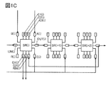
- FIGS. 1A to 1C are block diagrams illustrating a configuration of a flip-flop circuit according to an embodiment.
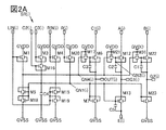
- 2A and 2B are circuit diagrams illustrating a configuration of a flip-flop circuit according to the embodiment.
- 3A and 3B are circuit diagrams illustrating a configuration of the flip-flop circuit according to the embodiment.
- FIGS. 4A and 4B are timing charts illustrating the operation of the drive circuit including the flip-flop circuit according to the embodiment.
- FIGS. 5A and 5B are timing charts for explaining the operation of the drive circuit including the flip-flop circuit according to the embodiment.
- FIG. 6 is a block diagram illustrating a configuration of a drive circuit according to the embodiment.
- 7A and 7B are diagrams illustrating a configuration of a display panel according to the embodiment.
- FIG. 8A and 8B are diagrams illustrating a configuration of a display panel according to the embodiment.
- FIG. 9 is a diagram illustrating a configuration of a display panel according to the embodiment.
- FIG. 10 is a block diagram illustrating a configuration of a display panel according to the embodiment.
- 11A and 11B are cross-sectional views illustrating a configuration of a display panel according to an embodiment.
- 12A and 12B are cross-sectional views illustrating a configuration of a display panel according to an embodiment.
- 13A to 13D are diagrams illustrating a configuration of a display device according to an embodiment.
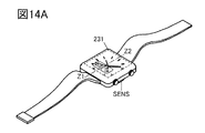
- 14A to 14C are diagrams illustrating a configuration of a display device according to an embodiment.
- FIG. 15 is a block diagram illustrating a configuration of the input / output device according to the embodiment.
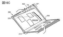
- FIG. 16A to FIG. 16C are a block diagram and a projection diagram illustrating the configuration of the information processing apparatus according to the embodiment.
- 17A and 17B are flowcharts illustrating a method for driving the information processing device according to the embodiment.
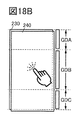
- 18A to 18C are diagrams illustrating a method for driving the information processing device according to the embodiment.
- FIGS. 19A to 19E are diagrams illustrating the configuration of the information processing apparatus according to the embodiment.
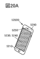
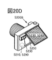
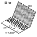
- 20A to 20E are diagrams illustrating the configuration of the information processing device according to the embodiment.
- FIGS. 21A and 21B are diagrams illustrating the configuration of the information processing apparatus according to the embodiment.
- FIG. 22 is a photograph illustrating a display state of the display device manufactured according to the example.
- a flip-flop circuit includes first to fifth input terminals and first to third output terminals.
- the first input terminal is supplied with a first trigger signal
- the second input terminal is supplied with a second trigger signal
- the third input terminal is supplied with a collective selection signal
- the fourth input terminal is supplied with a fourth trigger signal.
- One pulse width modulation signal is supplied
- a fifth input terminal is supplied with a second pulse width modulation signal.
- the first output terminal supplies the first selection signal based on the first pulse width modulation signal during a period from when the first trigger signal is supplied to when the second trigger signal is supplied.
- the first output terminal supplies the first selection signal while the batch selection signal is supplied, and the second output terminal supplies the second trigger signal after the first trigger signal is supplied.
- a second selection signal is supplied based on the second pulse width modulation signal
- a third output terminal supplies a third trigger signal.
- the first selection signal and the second selection signal can be supplied during a period from when the first trigger signal is supplied to when the second trigger signal is supplied.
- the first selection signal can be supplied during a period in which the batch selection signal is supplied.
- FIG. 1 is a block diagram illustrating a configuration of a flip-flop circuit of one embodiment of the present invention.
- 1A and 1B are block diagrams each illustrating a structure of a terminal included in a flip-flop circuit of one embodiment of the present invention.
- FIG. 1C illustrates an example of connecting a plurality of flip-flop circuits of one embodiment of the present invention.
- FIG. 2 is a diagram illustrating a configuration of a flip-flop circuit of one embodiment of the present invention.
- FIG. 2A is a circuit diagram of a flip-flop circuit of one embodiment of the present invention
- FIG. 2B is a circuit diagram of a flip-flop circuit that can be used by being connected to the flip-flop circuit of FIG. 2A.
- FIG. 3 is a diagram illustrating a configuration of a flip-flop circuit of one embodiment of the present invention.
- FIG. 3A is a circuit diagram of a flip-flop circuit of one embodiment of the present invention
- FIG. 3B is a circuit diagram of a flip-flop circuit that can be used by being connected to the flip-flop circuit of FIG. 3A.
- FIG. 4 illustrates the operation of the flip-flop circuit of one embodiment of the present invention.
- FIG. 4A is a timing chart illustrating operation of the driver circuit including the flip-flop circuit of one embodiment of the present invention illustrated in FIG. 2, and
- FIG. 4B includes the flip-flop circuit of one embodiment of the present invention illustrated in FIG. 5 is a timing chart illustrating an operation of a drive circuit.
- FIG. 5 illustrates the operation of the flip-flop circuit of one embodiment of the present invention.
- FIG. 5A is a timing chart illustrating operation of the driver circuit including the flip-flop circuit of one embodiment of the present invention illustrated in FIG. 2 which is different from FIG. 4A.
- FIG. 5B is a timing chart of FIG. 4B is a timing chart illustrating an operation of the driving circuit including the flip-flop circuit, which is different from the operation in FIG. 4B.
- a variable that takes an integer of 1 or more as a value may be used as a sign.
- (p) including a variable p having an integer value of 1 or more may be used as a part of a code that specifies any of up to p components.
- (m, n) including a variable m and a variable n each having an integer value of 1 or more may be used as a part of a code for specifying any one of up to m ⁇ n components.
- the flip-flop circuit SR (i) described in this embodiment includes an input terminal LIN (i), an input terminal RIN (i), an input terminal E (i), an input terminal A (i), and an input terminal LIN (i). It has a terminal B (i). Further, it has an output terminal G1 (i), an output terminal G2 (i), and an output terminal OUT (i) (see FIG. 1A). Further, it has a terminal C1 (i), a terminal C2 (i) and a terminal C3 (i). Note that one of the wirings CLK1 to CLK4 is selected and electrically connected to one of the terminals C1 (i) to C3 (i).
- the terminal C1 (i) is electrically connected to the wiring CLK1
- the terminal C2 (i) is electrically connected to the wiring CLK2
- the terminal C3 (i) is electrically connected to the wiring CLK3. Accordingly, a plurality of clock signals whose phases are shifted can be supplied to the terminals C1 (i) to C3 (i).
- the input terminal LIN (i) is supplied with a first trigger signal, and the input terminal RIN (i) is supplied with a second trigger signal (see FIG. 4A).
- the input terminal E (i) is supplied with a batch selection signal.
- the input terminal A (i) is supplied with a first pulse width modulation signal, and the input terminal B (i) is supplied with a second pulse width modulation signal.
- the output terminal G1 (i) supplies the first selection signal based on the first pulse width modulation signal during a period from when the first trigger signal is supplied to when the second trigger signal is supplied. I do. Further, the output terminal G1 (i) supplies the first selection signal during a period in which the collective selection signal is supplied (see FIGS. 4A and 5A).
- the output terminal G2 (i) supplies a second selection signal based on the second pulse width modulation signal during a period from when the first trigger signal is supplied to when the second trigger signal is supplied. I do.
- the output terminal OUT (i) supplies a third trigger signal.
- ⁇ Configuration Example of Flip-Flop Circuit 2. For example, using the transistors M1, M16, M3, M4, M6, M12, M22, M5, M15, M7, M13, and M23 in the flip-flop circuit SR (i) (See FIG. 2A). Further, the transistors M17, M21, M31, M18, and M19 can be used in the flip-flop circuit SR (i). Further, a capacitor C1, a capacitor C2, a capacitor C3, a capacitor C4, and a capacitor C5 can be used.
- the flip-flop circuit of one embodiment of the present invention can be formed using unipolar transistors.
- the transistor can be formed using a transistor that performs an n-type operation.
- Transistor M1, Transistor M15, Transistor M19 Each include a gate electrode to which a first trigger signal is supplied. Note that the transistor M1 has a function of supplying the potential of the wiring GVDD to the node GN4 (i) based on the first trigger signal.
- the transistors M15 and M19 have a function of supplying the potential of the wiring GVSS to the node GN1 (i) based on the first trigger signal. Thereby, the operation of the flip-flop circuit SR (i) can be started. Alternatively, the node GN1 (i) can be kept in a floating state until the potential of the wiring GVSS is supplied to the node GN1 (i).
- Transistor M4 has a gate electrode supplied with the second trigger signal. Note that the transistor M4 has a function of supplying the potential of the wiring GVDD to the node GN1 (i) based on the second trigger signal.
- Transistor M6, Transistor M12, Transistor M22 Each of the transistor M6, the transistor M12, and the transistor M22 includes a gate electrode electrically connected to the node GN4 (i). Note that the transistor M6 has a function of supplying a first clock signal to the output terminal OUT (i) based on the potential of the node GN4 (i), and the transistor M12 outputs a first pulse width modulation signal to the output terminal OUT (i). The transistor M22 has a function of supplying the second pulse width modulation signal to the output terminal G2 (i).
- Transistor M5 Transistor M18, Transistor M7, Transistor M13, Transistor M23
- Each of the transistor M5, the transistor M18, the transistor M7, the transistor M13, and the transistor M23 includes a gate electrode electrically connected to the node GN1 (i).
- the transistor M5 and the transistor M18 have a function of supplying the potential of the wiring GVSS to the node GN4 (i) based on the potential of the node GN1 (i), and the transistor M7 outputs the potential of the wiring GVSS to the output terminal OUT (i ),
- the transistor M13 has a function of supplying the potential of the input terminal E (i) to the output terminal G1 (i), and the transistor M23 supplies the potential of the wiring GVSS to the output terminal G2 (i). Provide functions.
- Transistor M16, Transistor M3 The transistor M16 has a gate electrode supplied with a second clock signal, and the transistor M3 has a gate electrode supplied with a third clock signal. Note that the transistor M16 and the transistor M3 have a function of supplying the potential of the wiring GVDD to the node GN1 (i) during the period in which the second clock signal and the third clock signal overlap.
- the transistor M20 includes a gate electrode electrically connected to the terminal R (i). Note that the transistor M20 supplies the potential of the wiring GVDD to the node GN1 (i) based on the potential of the terminal R (i). For example, a reset signal can be supplied to the terminal R (i). Thus, the flip-flop circuit SR (i) can be reset. Alternatively, the shift register circuit including the flip-flop circuit SR (i) can be reset. Note that the flip-flop circuit SR (i) can be reset using a clock signal.
- Transistor M17, Transistor M21, Transistor M31 Each include a gate electrode to which the potential of the wiring GVDD is supplied. Accordingly, for example, when the potential of the node GN4 (i) is higher than the potential of the wiring GVDD, stress applied to the transistors M6, M12, and M22 can be suppressed. Alternatively, the output can be stably supplied by using the node GN4 (i). Alternatively, stress applied between the first electrode and the second electrode of the transistor M1, the transistor M5, and the transistor M18 can be suppressed.
- the flip-flop circuit SR (m + 1) has the same configuration as the flip-flop circuit SR (i) except that the flip-flop circuit SR (m + 1) does not include the input terminal RIN (i) and the transistor M4 (FIGS. 1B and 2B). reference). Further, it can be used at the last stage of the shift register circuit. Note that a transistor having a wider region in which a channel is formed is more suitable for the flip-flop circuit SR (m + 1) than the transistor used for the flip-flop circuit SR (i).
- the width of the region where the channel of the transistor M3 or the transistor M16 included in the flip-flop circuit SR (m + 1) is formed is determined by the width of the channel of the transistor M3 or the transistor M16 included in the flip-flop circuit SR (i). Wider than the width of the area to be covered.
- the flip-flop circuit SR (i) described in this embodiment includes a transistor M13, a transistor M23, a transistor M7, a node GN1 (i), and a wiring GVSS (FIGS. 2A and 2B). , FIG. 3A and FIG. 3B).
- Transistor M13 is electrically connected to a gate electrode electrically connected to node GN1 (i), a first electrode electrically connected to output terminal G1 (i), and an input terminal E (i). A second electrode.
- the transistor M13 is off during the period from when the first trigger signal is supplied to when the second trigger signal is supplied.
- Transistor M23 has a gate electrode electrically connected to the node GN1 (i), a first electrode electrically connected to the output terminal G2 (i), and a second electrode electrically connected to the wiring GVSS. Is provided.
- the transistor M23 is off during a period from when the first trigger signal is supplied to when the second trigger signal is supplied.
- Transistor M7 has a gate electrode electrically connected to the node GN1 (i), a first electrode electrically connected to the output terminal OUT (i), and a second electrode electrically connected to the wiring GVSS. Is provided.
- the transistor M7 is off during the period from when the first trigger signal is supplied to when the second trigger signal is supplied.
- the first selection signal and the second selection signal can be supplied during a period from when the first trigger signal is supplied to when the second trigger signal is supplied.
- the first selection signal can be supplied during a period in which the batch selection signal is supplied.
- the flip-flop circuit SR (i) described in this embodiment includes a transistor M24 and a wiring GVDD (see FIGS. 3A and 3B).
- the transistor M24 includes a gate electrode electrically connected to the wiring GVDD, a first electrode electrically connected to the node GN1 (i), and a second electrode electrically connected to the gate electrode of the transistor M13. , Is provided.
- the transistor M24 can be turned off in a period TB during which the collective selection signal is high, excluding a period from when the first trigger signal is supplied to when the second trigger signal is supplied. (See FIG. 3B or 4B).
- the potential of the node GN1 (i) can be suppressed to be lower than the potential obtained by subtracting the threshold voltage of the transistor M24 from the potential supplied from the wiring GVDD.
- a rise in potential of the node GN1 (i) applied to the transistor M23, the transistor M7, the transistor M5, and the transistor M18 can be suppressed.
- stress caused by an increase in the potential of the node GN1 (i) on the transistor M15 and the transistor M19 can be suppressed.
- a novel flip-flop circuit having excellent convenience, usefulness, or reliability can be provided.
- the potential of the node GN2 (i) >> The potential of the wiring GVDD is supplied to the node GN2 (i) during a period in which the first trigger signal is high (see FIGS. 2A, 2B, and 4AT1).
- the first trigger signal and the second trigger signal are low, and the potential of the node GN1 (i) is obtained by adding the threshold voltage of the transistor M5 to the potential supplied by the wiring GVDD.
- the floating state is maintained (see AT2 in FIG. 4).
- node GN2 (i) is capacitively coupled to the output terminal G1 (i) via, for example, the capacitor C2.
- the potential of the node GN1 (i) >> The potential of the wiring GVSS is supplied to the node GN1 (i) during a period in which the first trigger signal is high (see FIGS. 2A, 2B, and 4AT1). Further, the node GN1 (i) maintains a floating state during a period in which the first trigger signal and the second trigger signal are low (see AT2 in FIG. 4).
- the node GN1 (i) is capacitively coupled to the input terminal E (i) via the capacitor C5.
- the potential of the node GN1 (i) is affected by the potential of the input terminal E (i).
- the potential of the node GN1 (i) rises, for example, under the influence of the batch selection signal (see FIGS. 2A, 2B, and 4AT3).
- the potential of the node GN1 (i) approaches, for example, a potential obtained by adding a voltage supplied by the collective selection signal to a potential supplied by the wiring GVDD.
- the flip-flop circuit SR (i) includes the transistor M24
- the potential of the node GN3 (i) is affected by the potential of the input terminal E (i).
- the potential of the node GN3 (i) rises, for example, under the influence of the batch selection signal (see FIGS. 3A, 3B, and 4BT3).
- the potential of the node GN3 (i) approaches, for example, a potential obtained by adding a voltage at which the collective selection signal is high to the potential supplied from the wiring GVDD.
- the transistor M24 is turned off.
- the influence of the batch selection signal on the potential of the node GN1 (i) can be suppressed.
- the potential of the node GN1 (i) can be suppressed to be lower than a potential obtained by subtracting a threshold voltage of the transistor M24 from a voltage supplied from the wiring GVDD.
- the influence of the batch selection signal on the potential of the node GN1 (i) can be eliminated.
- stress applied to a transistor including a gate electrode electrically connected to the node GN1 (i) can be suppressed.
- stress applied to the transistors M13, M23, M7, M5, and M18 can be suppressed.
- stress applied to the transistor M15 and the transistor M19 can be suppressed.
- stress applied to the transistor M16, the transistor M4, and the transistor M20 can be suppressed.
- a novel flip-flop circuit having excellent convenience, usefulness, or reliability can be provided.
- FIG. 6 is a block diagram illustrating a structure of a driver circuit of one embodiment of the present invention.
- the drive circuit GD described in this embodiment includes a group of flip-flop circuits SR (1) to SR (m + 2) and a wiring VEE (see FIG. 6). Further, a wiring RES, a wiring DUM1 (1), a wiring DUM2 (1), a wiring DUM1 (2), and a wiring DUM2 (2) are provided.
- the group of flip-flop circuits SR (1) to SR (m + 2) includes the flip-flop circuit SR (i), the flip-flop circuit SR (i + 1), and the flip-flop circuit described in Embodiment 1. SR (i + 2).
- Flip-flop circuit SR (i + 1) is electrically connected to the flip-flop circuit SR (i), and the flip-flop circuit SR (i + 1) is supplied with a third trigger signal (see FIG. 1C).
- Flip-flop circuit SR (i + 1) is electrically connected to flip-flop circuit SR (i + 2).
- the flip-flop circuit SR (i + 2) supplies a second trigger signal.
- Wiring VEE supplies a batch selection signal, and the wiring VEE is electrically connected to the group of flip-flop circuits SR (1) to SR (m + 2).
- the group of flip-flop circuits can supply the first selection signals in a predetermined order.
- a group of flip-flop circuits can supply the second selection signals in a predetermined order.
- a group of flip-flop circuits can supply the first selection signal all at once.
- the input terminal LIN (i) is electrically connected to the wiring SPL or the output terminal OUT (i-1) of the flip-flop circuit SR (i-1) (see FIGS. 1C and 6).
- the wiring SPL supplies a start pulse signal
- the output terminal OUT (i-1) of the flip-flop circuit SR (i-1) supplies a first trigger signal.
- the input terminal RIN (i) is electrically connected to OUT (i + 2) of the flip-flop circuit SR (i + 2). Note that the output terminal OUT (i + 2) of the flip-flop circuit SR (i + 2) supplies a second trigger signal.
- the input terminal E (i) is electrically connected to the wiring VEE. Note that the wiring VEE supplies a collective selection signal.
- the input terminal A (i) is electrically connected to any one of the wirings PWCA1 to PWCA4.
- each of the wirings PWCA1 to PWCA4 supplies a first pulse width modulation signal.
- a square wave can be used for the first pulse width modulation signal (see FIG. 4A or 5A).
- the input terminal B (i) is electrically connected to any one of the wirings PWCB1 to PWCB4.
- the wirings PWCB1 to PWCB4 each supply a pulse width modulation signal.
- the same signal as the first pulse width modulation signal can be used for the second pulse width modulation signal (see FIG. 4A).
- a signal having a pulse width different from that of the first pulse width modulation signal can be used for the second pulse width modulation signal.
- a signal having a shorter pulse width than the first pulse width modulation signal can be used for the second pulse width modulation signal (see FIG. 5A).
- the output terminal G1 (i) is electrically connected to the scanning line GL1 (i), and the output terminal G2 (i) is electrically connected to the scanning line GL2 (i) (see FIGS. 1C and 6).
- the output terminal OUT (i) is electrically connected to LIN (i + 1) of the flip-flop circuit SR (i + 1) and RIN (i) of the flip-flop circuit SR (i-2) (see FIG. 6).
- the driver circuit GD supplies the selection signals in order. For example, during the period TA, the flip-flop circuits SR (1) to SR (m + 2) sequentially supply selection signals (see FIGS. 4A and 5A).
- the driving circuit GD of one embodiment of the present invention supplies a collective selection signal. For example, during the period TB, the flip-flop circuits SR (1) to SR (m + 2) simultaneously supply a selection signal.
- a period including the period TA and the period TB can be referred to as one subframe (SUB FRAME) period.
- a period LIGHT for turning on the light source can be provided after the end of one subframe period (see FIGS. 4A and 5A).
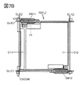
- FIG. 7 illustrates a structure of a display panel of one embodiment of the present invention.
- FIG. 7A is a top view of a display panel of one embodiment of the present invention, and
- FIG. 7B is a part of FIG. 7A.
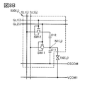
- FIG. 8 illustrates a structure of a display panel of one embodiment of the present invention.
- FIG. 8A is a cross-sectional view taken along section lines X1-X2, X3-X4, X9-X10 and pixels of FIG. 7A
- FIG. 8B is a circuit diagram illustrating the configuration of the pixel circuit 530 (i, j).
- FIG. 10 illustrates a structure of a display panel of one embodiment of the present invention.
- the display panel described in this embodiment includes a display region 231 and the driver circuit GD described in Embodiment 2 (see FIG. 10).
- the display area 231 includes a scanning line GL1 (i), a scanning line GL2 (i), a signal line SL1 (j), a signal line SL2 (j), and a pixel 702 (i, j).
- the pixel 702 (i, j) includes a display element 750 (i, j) and a pixel circuit 530 (i, j) (see FIG. 8A).
- the display element 750 (i, j) is electrically connected to the pixel circuit 530 (i, j) (see FIGS. 8A and 8B).
- an element which controls light reflection, light transmission, or light emission can be used for a display element.
- an electro-optical element or a light-emitting element can be used for a display element.
- the pixel circuit 530 (i, j) is electrically connected to the scanning line GL1 (i), the scanning line GL2 (i), the signal line SL1 (j), and the signal line SL2 (j) (see FIG. 8B).
- the scanning line GL1 (i) is electrically connected to the output terminal G1 (i), and the scanning line GL2 (i) is electrically connected to the output terminal G2 (i) (see FIG. 6).
- the first selection signal can be supplied to the first scanning line GL1 (i).
- a second selection signal can be supplied to the second scanning line GL2 (i).
- the pixel 702 (i, j) can be driven using the first selection signal or the second selection signal.
- a switch for example, a switch, a transistor, a diode, a resistor, an inductor, a capacitor, or the like can be used for the pixel circuit 530 (i, j).
- a transistor can be used for a switch.
- the other semiconductor film can be formed in a step of forming a semiconductor film of one transistor.
- the pixel 702 (i, j) can use a liquid crystal element as the display element 750 (i, j).
- the pixel circuit 530 (i, j) includes a capacitor C11, a switch SW11, and a node N1 (i, j) (see FIG. 8B).
- the switch SW11 has a first terminal electrically connected to the signal line SL2 (j), and has a second terminal electrically connected to the first electrode of the display element 750 (i, j). .
- the switch SW11 has a function of switching between a conductive state and a non-conductive state based on a selection signal.
- the capacitor C11 includes a first electrode electrically connected to the second terminal of the switch SW11, and a second electrode electrically connected to the conductive film CSCOM.
- the display element 750 (i, j) performs display based on the potential VN of the node N1 (i, j).
- the pixel circuit 530 (i, j) includes a capacitor C11, a capacitor C12, a switch SW11, a switch SW12, and a node N1 (i, j).
- the switch SW11 has a first terminal electrically connected to the signal line SL2 (j), and has a second terminal electrically connected to the first electrode of the display element 750 (i, j). . Note that the switch SW11 has a function of switching between a conductive state and a non-conductive state based on the second selection signal.
- the capacitor C11 includes a first electrode electrically connected to the second terminal of the switch SW11, and a second electrode electrically connected to the conductive film CSCOM.
- the switch SW12 has a first terminal that is electrically connected to the signal line SL1 (j).
- the switch SW12 has a function of switching between a conductive state and a non-conductive state based on a first selection signal.
- the capacitor C12 includes a first electrode that is electrically connected to a second terminal of the switch SW12, and a second electrode that is electrically connected to a second terminal of the switch SW11.
- the display element 750 (i, j) performs display based on the potential VN of the node N1 (i, j).
- the switch SW12 when the switch SW11 is in a non-conductive state, the switch SW12 can be changed from a non-conductive state to a conductive state. Further, when the switch SW11 is off, the switch SW12 can be changed from the on state to the off state.
- the switches SW11 and SW12 are turned on. For example, a first selection signal is supplied to the scanning line GL1 (i), and a second selection signal is supplied to the scanning line GL2 (i).
- the image signal is supplied to the capacitor C12.
- an image signal is supplied using a potential difference between a potential supplied from the signal line SL1 (j) and a potential supplied from the signal line SL2 (j).
- the switch SW12 is turned on while the switch SW11 is kept off.
- a collective selection signal is supplied to the scanning line GL1 (i).
- a predetermined potential is supplied to the signal line SL1 (i), and the potential of the node N1 (i, j) is offset via the capacitor C12.
- the potential of the node N1 (i, j) can be controlled using the switches SW11 and SW12.
- the potential of the node N1 (i, j) can be controlled using the switch SW11, and the potential of the node N1 (i, j) can be changed using the switch SW12.
- a changing potential can be supplied to the display element 750 (i, j).
- display can be performed based on a changing potential.
- the display of the display element 750 (i, j) can be changed.
- the operation of the display element 750 (i, j) can be emphasized.
- the response of the display element 750 (i, j) can be accelerated.
- a novel display panel which is excellent in convenience, usefulness, or reliability can be provided.
- a high voltage can be supplied to the display element 750 (i, j).
- a large electric field can be applied to the layer 753 containing a liquid crystal material of the display element 750 (i, j).
- the alignment of the polymer-stabilized liquid crystal material can be controlled. As a result, a novel input / output device with excellent convenience, usefulness, or reliability can be provided.
- the pixel 702 (i, j) can use a light-emitting element as the display element 750 (i, j) (see FIG. 9).
- a light-emitting element for example, an organic EL element can be used for the display element 750 (i, j).
- the pixel circuit 530 (i, j) includes a transistor M, a capacitor C21, a switch SW21, a node N1 (i, j), a capacitor C22, and a switch SW22 (see FIG. 9). Further, the pixel circuit 530 (i, j) includes a node N2 (i, j), a switch SW23, and a switch SW24.
- the transistor M includes a first electrode that is electrically connected to the conductive film ANO.
- the capacitor C21 includes a first electrode electrically connected to a gate electrode of the transistor M, and a second electrode electrically connected to a second electrode of the transistor M.
- the switch SW21 has a first terminal electrically connected to the signal line SL2 (j), and has a second terminal electrically connected to the gate electrode of the transistor M.
- the switch SW21 has a function of switching between a conductive state and a non-conductive state based on the second selection signal.
- the capacitor C22 includes a first electrode that is electrically connected to a gate electrode of the transistor M.
- the switch SW22 includes a first terminal electrically connected to the signal line SL1 (j), and includes a second terminal electrically connected to a second electrode of the capacitor C22.
- the switch SW22 has a function of switching between a conductive state and a non-conductive state based on a first selection signal.
- the switch SW23 includes a first terminal electrically connected to the second electrode of the transistor M, and a second terminal electrically connected to the conductive film V0.
- the switch SW23 has a function of switching between a conductive state and a non-conductive state based on the first selection signal.
- the switch SW24 includes a first terminal electrically connected to the second electrode of the transistor M, and a second terminal electrically connected to the display element 750 (i, j).
- the switch SW24 has a function of switching between a conductive state and a non-conductive state based on a third selection signal. Note that the third selection signal can be supplied using the scanning line GL3 (i).
- the switch SW22 can be changed from the non-conductive state to the conductive state. Further, when the switch SW21 is in the non-conductive state, the switch SW22 can be changed from the conductive state to the non-conductive state.
- the display element 750 (i, j) performs display based on the potential VN of the node N1 (i, j).
- the potential of the node N1 (i, j) can be controlled using the switches SW21 and SW22.
- the potential of the node N1 (i, j) can be controlled using the switch SW21, and the potential of the node N1 (i, j) can be changed using the switch SW22.
- a changing potential can be supplied to the display element 750 (i, j).
- display can be performed based on a changing potential.
- the display of the display element 750 (i, j) can be changed.
- the operation of the display element 750 (i, j) can be emphasized.
- the response of the display element 750 (i, j) can be accelerated.
- a novel display panel which is excellent in convenience, usefulness, or reliability can be provided.
- the display region 231 includes a group of pixels 702 (i, 1) to 702 (i, n) and another group of pixels 702 (1, j) to 702 (m, j) (see FIG. 10).
- the display region 231 has a conductive film CSCOM and a conductive film VCOM1.
- a group of pixels 702 (i, 1) to 702 (i, n) are arranged in a row direction (a direction indicated by an arrow R1 in the drawing), and a group of pixels 702 (i, 1) to 702 (i). , N) includes a pixel 702 (i, j).
- the other group of pixels 702 (1, j) to 702 (m, j) are arranged in a column direction (direction indicated by an arrow C1 in the drawing) that intersects the row direction, and the other group of pixels 702 (1, j).
- (1, j) to pixel 702 (m, j) include pixel 702 (i, j).
- the scanning line GL1 (i) is electrically connected to the group of pixels 702 (i, 1) to 702 (i, n), and the scanning line GL2 (i) is connected to the group of pixels 702 (i, 1) to 702. (I, n).
- the signal line SL1 (j) is electrically connected to another group of pixels 702 (1, j) to 702 (m, j), and the signal line SL2 (j) is connected to another group of pixels 702 (1,1). j) to the pixel 702 (m, j).
- image information can be supplied to a plurality of pixels.
- a novel display panel which is excellent in convenience, usefulness, or reliability can be provided.
- the driving circuit GDA and the driving circuit GDB can be used for the driving circuit GD.
- the driver circuits GDA and GDB have a function of supplying a selection signal based on the control signal SP.
- a function of supplying a selection signal to one scanning line at a frequency of 30 Hz or more, preferably 60 Hz or more based on the control signal SP is provided. Thereby, a moving image can be displayed smoothly.
- a function of supplying a selection signal to one scanning line at a frequency of less than 30 Hz, preferably less than 1 Hz, and more preferably less than once per minute based on the control signal SP is provided. Thereby, a still image in which flicker is suppressed can be displayed.
- the frequency at which the driving circuit GDA supplies a selection signal can be different from the frequency at which the driving circuit GDB supplies a selection signal.
- the selection signal can be supplied to another area for displaying a moving image at a higher frequency than the frequency for supplying the selection signal to one area for displaying a still image.
- a still image in which flicker is suppressed can be displayed in one area, and a moving image can be smoothly displayed in another area.
- the frame frequency can be made variable.
- display can be performed at a frame frequency of 1 Hz or more and 120 Hz or less.
- display can be performed at a frame frequency of 120 Hz using a progressive method.
- the drive circuit SD has a function of generating an image signal based on the information V11 and a function of supplying the image signal to a pixel circuit electrically connected to one display element (see FIG. 10).
- various sequential circuits such as a shift register can be used for the drive circuit SD.
- an integrated circuit formed over a silicon substrate can be used for the drive circuit SD.
- the integrated circuit can be connected to the terminal by using a COG (Chip-on-glass) method or a COF (Chip-on-Film) method.
- COG Chip-on-glass
- COF Chip-on-Film
- an integrated circuit can be connected to a terminal using an anisotropic conductive film.
- FIG. 11 illustrates a structure of a display panel of one embodiment of the present invention.
- FIG. 11A is a cross-sectional view of the pixel 702 (i, j) taken along a cutting line Y1-Y2 in FIG. 7B
- FIG. 11B is a cross-sectional view illustrating a part of FIG.
- FIG. 12 illustrates a structure of a display panel of one embodiment of the present invention.
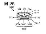
- FIG. 12A is a cross-sectional view taken along section lines X1-X2 and X3-X4 of FIG. 7A
- FIG. 12B is a cross-sectional view illustrating a part (MG1) of FIG. 12A.
- the display panel described in this embodiment includes a functional layer 520 (see FIG. 8A).
- Functional layer 520 includes drive circuit GD described in Embodiment 2 and pixel circuit 530 (i, j) described in Embodiment 3. Note that the functional layer 520 includes an opening 591A, and the pixel circuit 530 (i, j) is electrically connected to the display element 750 (i, j) at the opening 591A.
- a semiconductor film used for a transistor of the pixel circuit 530 can be formed.
- the number of parts can be reduced.
- a novel display panel which is excellent in convenience, usefulness, or reliability can be provided.
- Transistor configuration example For example, a bottom-gate transistor or a top-gate transistor can be used for the driver circuit GD and the pixel circuit 530 (i, j) (see FIGS. 11 and 12).
- the transistor includes a semiconductor film 508, a conductive film 504, a conductive film 512A, and a conductive film 512B (see FIG. 11B).
- the semiconductor film 508 includes a region 508A electrically connected to the conductive film 512A and a region 508B electrically connected to the conductive film 512B.
- the semiconductor film 508 includes a region 508C between the region 508A and the region 508B.
- the conductive film 504 includes a region overlapping with the region 508C, and the conductive film 504 has a function of a gate electrode.
- the insulating film 506 includes a region sandwiched between the semiconductor film 508 and the conductive film 504.
- the insulating film 506 has a function of a gate insulating film.
- the conductive film 512A has one of a source electrode function and a drain electrode function
- the conductive film 512B has the other of a source electrode function and a drain electrode function.
- the conductive film 524 can be used for a transistor.
- the conductive film 524 includes a region where the semiconductor film 508 is sandwiched between the conductive film 524 and the conductive film 504.
- the conductive film 524 has a function of a second gate electrode.
- the conductive film 524 can be electrically connected to the conductive film 504, for example. Note that the conductive film 524 can be used for the scan line GL2 (i).
- a semiconductor film used for the transistor of the driver circuit GD can be formed.
- a semiconductor containing a Group 14 element can be used for the semiconductor film 508.
- a semiconductor containing silicon can be used for the semiconductor film 508.
- Hydroated amorphous silicon can be used for the semiconductor film 508.
- microcrystalline silicon or the like can be used for the semiconductor film 508.
- a display panel with less display unevenness than a display panel using polysilicon for the semiconductor film 508 can be provided.
- the size of the display panel can be easily increased.
- polysilicon can be used for the semiconductor film 508.
- the field-effect mobility of the transistor can be higher than that of a transistor using hydrogenated amorphous silicon for the semiconductor film 508.
- the driving capability can be higher than that of a transistor using hydrogenated amorphous silicon for the semiconductor film 508.
- the aperture ratio of a pixel can be higher than that of a transistor using hydrogenated amorphous silicon for the semiconductor film 508.
- the reliability of a transistor can be higher than that of a transistor using hydrogenated amorphous silicon for the semiconductor film 508.
- the temperature required for manufacturing the transistor can be lower than that of a transistor using single crystal silicon, for example.
- a semiconductor film used for a transistor of a driver circuit can be formed in the same step as a semiconductor film used for a transistor of a pixel circuit.
- a driver circuit can be formed over the same substrate as a substrate over which a pixel circuit is formed. Alternatively, the number of components constituting the electronic device can be reduced.
- Single-crystal silicon For example, single crystal silicon can be used for the semiconductor film 508. Accordingly, for example, the definition can be higher than that of a display panel using hydrogenated amorphous silicon for the semiconductor film 508. Alternatively, for example, a display panel with less display unevenness than a display panel in which polysilicon is used for the semiconductor film 508 can be provided. Or, for example, a smart glass or head mounted display can be provided.
- a metal oxide can be used for the semiconductor film 508.
- the time during which the pixel circuit can hold an image signal can be longer than that of a pixel circuit using a transistor using amorphous silicon for a semiconductor film.
- the selection signal can be supplied at a frequency of less than 30 Hz, preferably less than 1 Hz, and more preferably less than once per minute, while suppressing the occurrence of flicker. As a result, fatigue accumulated in the user of the information processing device can be reduced. Further, power consumption associated with driving can be reduced.
- a transistor including an oxide semiconductor can be used.
- an oxide semiconductor containing indium or an oxide semiconductor containing indium, gallium, and zinc can be used for the semiconductor film.
- a transistor having a smaller leak current in an off state than a transistor including amorphous silicon for a semiconductor film can be used.
- a transistor including an oxide semiconductor for a semiconductor film can be used.
- a 25-nm-thick film containing indium, gallium, and zinc can be used for the semiconductor film 508.
- a conductive film in which a 10-nm-thick film containing tantalum and nitrogen and a 300-nm-thick film containing copper are stacked can be used for the conductive film 504.
- the film containing copper has a region which sandwiches a film containing tantalum and nitrogen between the insulating film 506 and the insulating film 506.
- a stacked film in which a 400-nm-thick film containing silicon and nitrogen and a 200-nm-thick film containing silicon, oxygen, and nitrogen are stacked can be used for the insulating film 506.
- the film containing silicon and nitrogen includes a region where the film containing silicon, oxygen, and nitrogen is provided between the semiconductor film 508 and the semiconductor film 508.
- the film including tungsten has a region in contact with the semiconductor film 508.
- a production line of a bottom-gate transistor using amorphous silicon for a semiconductor can be easily converted to a production line of a bottom-gate transistor using an oxide semiconductor for a semiconductor.
- a production line of a top-gate transistor using polysilicon as a semiconductor can be easily modified to a production line of a top-gate transistor using an oxide semiconductor as a semiconductor. Both modifications can effectively utilize existing production lines.
- a compound semiconductor can be used for a semiconductor of a transistor.
- a semiconductor containing gallium arsenide can be used.
- an organic semiconductor can be used for a semiconductor of a transistor.
- an organic semiconductor containing polyacenes or graphene can be used for the semiconductor film.
- the capacitor includes one conductive film, another conductive film, and an insulating film.
- the insulating film includes a region sandwiched between one conductive film and another conductive film.
- the conductive film 504, the conductive film 512A, and the insulating film 506 can be used for a capacitor.
- the capacitor C12 includes a conductive film 754 (i, j), an electrode 751 (i, j), and an insulating film 521B (see FIG. 11A).
- the functional layer 520 includes an insulating film 521, an insulating film 518, an insulating film 516, an insulating film 506, an insulating film 501C, and the like (see FIG. 11A).
- the insulating film 521 includes a region sandwiched between the pixel circuit 530 (i, j) and the display element 750 (i, j).
- the insulating film 518 includes a region interposed between the insulating film 521 and the insulating film 501C.
- the insulating film 516 includes a region interposed between the insulating film 518 and the insulating film 501C.
- the insulating film 506 includes a region interposed between the insulating film 516 and the insulating film 501C.
- Insulating film 521 For example, an insulating inorganic material, an insulating organic material, or an insulating composite material containing an inorganic material and an organic material can be used for the insulating film 521.
- the insulating film 521 can be formed using an inorganic oxide film, an inorganic nitride film, an inorganic oxynitride film, or the like, or a stacked material in which a plurality of layers selected from the above are stacked.
- a silicon oxide film, a silicon nitride film, a silicon oxynitride film, an aluminum oxide film, or a film including a stacked material in which a plurality of layers selected from the above can be used for the insulating film 521.
- the silicon nitride film is a dense film and has an excellent function of suppressing diffusion of impurities.
- a polyester, polyolefin, polyamide, polyimide, polycarbonate, polysiloxane, acrylic resin, or the like, or a stacked material or a composite material of a plurality of resins selected from the above can be used for the insulating film 521. Further, it may be formed using a photosensitive material. Accordingly, in the insulating film 521, for example, steps caused by various structures overlapping with the insulating film 521 can be flattened.
- polyimide has characteristics superior to other organic materials in characteristics such as thermal stability, insulating properties, toughness, low dielectric constant, low coefficient of thermal expansion, and chemical resistance.
- polyimide can be particularly preferably used for the insulating film 521 and the like.
- a film formed using a photosensitive material can be used for the insulating film 521.
- a film formed using photosensitive polyimide, photosensitive acrylic resin, or the like can be used for the insulating film 521.
- the insulating film 518 including a material which can be used for the insulating film 521 can be used.
- a material having a function of suppressing diffusion of oxygen, hydrogen, water, an alkali metal, an alkaline earth metal, or the like can be used for the insulating film 518.
- a nitride insulating film can be used for the insulating film 518.
- silicon nitride, silicon nitride oxide, aluminum nitride, aluminum nitride oxide, or the like can be used for the insulating film 518.
- diffusion of impurities into the semiconductor film of the transistor can be suppressed.
- Insulating film 516 For example, a material that can be used for the insulating film 521 can be used for the insulating film 516.
- a film whose manufacturing method is different from that of the insulating film 518 can be used for the insulating film 516.
- Insulating film 506 For example, a material that can be used for the insulating film 521 can be used for the insulating film 506.
- a film including a lanthanum oxide film, a cerium oxide film, or a neodymium oxide film can be used for the insulating film 506.
- Insulating film 501C For example, a material that can be used for the insulating film 521 can be used for the insulating film 501C. Specifically, a material containing silicon and oxygen can be used for the insulating film 501C. Thus, diffusion of impurities into a pixel circuit, a display element, or the like can be suppressed.
- the functional layer 520 includes a conductive film, a wiring, and a terminal.
- a material having conductivity can be used for a wiring, an electrode, a terminal, a conductive film, or the like.
- an inorganic conductive material, an organic conductive material, a metal, a conductive ceramic, or the like can be used for the wiring and the like.
- a metal element selected from aluminum, gold, platinum, silver, copper, chromium, tantalum, titanium, molybdenum, tungsten, nickel, iron, cobalt, palladium, or manganese can be used for the wiring and the like.
- an alloy containing the above-described metal element can be used for a wiring or the like.
- an alloy of copper and manganese is suitable for fine processing using a wet etching method.
- a two-layer structure in which a titanium film is stacked over an aluminum film a two-layer structure in which a titanium film is stacked over a titanium nitride film, a two-layer structure in which a tungsten film is stacked over a titanium nitride film, a tantalum nitride film, or A two-layer structure in which a tungsten film is stacked over a tungsten nitride film, a titanium film, a three-layer structure in which an aluminum film is stacked over the titanium film, and a titanium film is further formed thereon can be used for wiring or the like. .
- a conductive oxide such as indium oxide, indium tin oxide, indium zinc oxide, zinc oxide, or zinc oxide to which gallium is added can be used for the wiring and the like.
- a film containing graphene or graphite can be used for a wiring or the like.
- a film containing graphene oxide is formed, and the film containing graphene oxide is reduced; thus, a film containing graphene can be formed.
- the method of reduction include a method of applying heat and a method of using a reducing agent.
- a film including metal nanowires can be used for a wiring or the like.
- a nanowire containing silver can be used.
- a conductive polymer can be used for a wiring or the like.
- the terminal 519B can be electrically connected to the flexible printed circuit board FPC1 using the conductive material ACF1 (see FIG. 8A). Specifically, the terminal 519B can be electrically connected to the flexible printed circuit board FPC1 using the conductive material CP.
- the display panel 700 includes a base 510, a base 770, and a sealing material 705 (see FIG. 12A).
- Base 510, Base 770 A material having a light-transmitting property can be used for the base 510 or the base 770.
- a flexible material can be used for the base material 510 or the base material 770. Accordingly, a display panel having flexibility can be provided.
- a material having a thickness of 0.7 mm or less and a thickness of 0.1 mm or more can be used.
- a material polished to a thickness of about 0.1 mm can be used. Thereby, the weight can be reduced.
- glass substrates of the sixth generation (1500 mm ⁇ 1850 mm), the seventh generation (1870 mm ⁇ 2200 mm), the eighth generation (2200 mm ⁇ 2400 mm), the ninth generation (2400 mm ⁇ 2800 mm), the tenth generation (2950 mm ⁇ 3400 mm), etc.
- the base material 510 or the base material 770 can be used for the base material 510 or the base material 770.
- a large-sized display device can be manufactured.
- An organic material, an inorganic material, a composite material of an organic material and an inorganic material, or the like can be used for the base 510 or the base 770.
- inorganic materials such as glass, ceramics, and metals can be used.
- non-alkali glass, soda-lime glass, potash glass, crystal glass, aluminosilicate glass, tempered glass, chemically tempered glass, quartz, sapphire, or the like can be used for the base 510 or the base 770.
- aluminosilicate glass, tempered glass, chemically strengthened glass, sapphire, or the like can be suitably used for the base material 510 or the base material 770 disposed on the side closer to the user of the display panel. This can prevent the display panel from being damaged or damaged during use.
- an inorganic oxide film, an inorganic nitride film, an inorganic oxynitride film, or the like can be used.
- a silicon oxide film, a silicon nitride film, a silicon oxynitride film, an aluminum oxide film, or the like can be used.
- Stainless steel or aluminum or the like can be used for the substrate 510 or the substrate 770.
- a single crystal semiconductor substrate made of silicon or silicon carbide, a polycrystalline semiconductor substrate, a compound semiconductor substrate such as silicon germanium, an SOI substrate, or the like can be used for the base 510 or the base 770. Accordingly, a semiconductor element can be formed over the base 510 or the base 770.
- an organic material such as a resin, a resin film, or plastic can be used for the base 510 or the base 770.
- a material containing polyester, polyolefin, polyamide (eg, nylon or aramid), polyimide, polycarbonate, polyurethane or acrylic resin, epoxy resin, or a resin having a siloxane bond is used for the base material 510 or the base material 770.
- a resin film, a resin plate, a laminated material, or the like containing these materials can be used. Thereby, the weight can be reduced. Alternatively, for example, the frequency of occurrence of breakage or the like due to a drop can be reduced.
- PET polyethylene terephthalate
- PEN polyethylene naphthalate
- PES polyether sulfone
- COP cycloolefin polymer
- COC cycloolefin copolymer
- a composite material in which a film such as a metal plate, a thin glass plate, or an inorganic material is bonded to a resin film or the like can be used for the base 510 or the base 770.
- a composite material in which fibrous or particulate metal, glass, an inorganic material, or the like is dispersed in a resin can be used for the base material 510 or the base material 770.
- a composite material in which a fibrous or particulate resin or an organic material is dispersed in an inorganic material can be used for the base material 510 or the base material 770.
- a single-layer material or a material in which a plurality of layers are stacked can be used for the base 510 or the base 770.
- a material in which an insulating film or the like is stacked can be used.
- a material in which one or more films selected from a silicon oxide layer, a silicon nitride layer, a silicon oxynitride layer, or the like can be used.
- paper, wood, or the like can be used for the base 510 or the base 770.
- a material having heat resistance high enough to withstand heat treatment in the manufacturing process can be used for the base material 510 or the base material 770.
- a material having heat resistance to heat applied during a manufacturing process for directly forming a transistor, a capacitor, or the like can be used for the base 510 or the base 770.
- an insulating film, a transistor, a capacitor, or the like is formed over a process substrate having heat resistance to heat applied during a manufacturing process, and the formed insulating film, the transistor, the capacitor, or the like is formed on, for example, the base material 510 or the base material. 770 can be used.
- an insulating film, a transistor, a capacitor, or the like can be formed over a flexible substrate.
- the sealant 705 has a region sandwiched between the functional layer 520 and the base 770, and has a function of bonding the functional layer 520 and the base 770 (see FIG. 12).
- An inorganic material, an organic material, a composite material of an inorganic material and an organic material, or the like can be used for the sealant 705.
- an organic material such as a heat-meltable resin or a curable resin can be used for the sealant 705.
- an organic material such as a reaction-curable adhesive, a light-curable adhesive, a thermosetting adhesive, and / or an anaerobic adhesive can be used for the sealant 705.
- an adhesive containing an epoxy resin, an acrylic resin, a silicone resin, a phenol resin, a polyimide resin, an imide resin, a PVC (polyvinyl chloride) resin, a PVB (polyvinyl butyral) resin, an EVA (ethylene vinyl acetate) resin, or the like can be used for the sealing material 705.
- the display panel 700 includes the structure KB1 or the functional film 770P (see FIG. 11A). Note that a coloring film, a light-blocking film, or the like can be used between the functional layer 520 and the base 770.
- the structure KB1 includes a region sandwiched between the functional layer 520 and the base 770.
- the structure KB1 has a function of providing a predetermined gap between the functional layer 520 and the base material 770.
- the functional film 770P includes a region overlapping with the display element 750 (i, j).
- an anti-reflection film, a polarizing film, a retardation film, a light diffusion film, a light condensing film, or the like can be used for the functional film 770P.
- an antireflection film having a thickness of 1 ⁇ m or less can be used for the functional film 770P.
- a laminated film in which three or more dielectric layers are stacked, preferably five or more layers, and more preferably 15 or more layers can be used for the functional film 770P.
- the reflectance can be suppressed to 0.5% or less, preferably 0.08% or less.
- a circularly polarizing film can be used for the functional film 770P.
- an antistatic film that suppresses the adhesion of dust a water-repellent film that makes it difficult to adhere dirt, an oil-repellent film that makes it difficult to adhere dirt, an antireflection film (anti-reflection film), and a non-glossy treatment film (anti- (Glare film), a hard coat film that suppresses generation of scratches during use, a self-healing film that suppresses generation of scratches during use, and the like can be used for the functional film 770P.
- ⁇ Configuration example of display element For example, an element which controls light reflection, light transmission, or light emission can be used for a display element. Specifically, an electro-optical element or a light-emitting element can be used for a display element.
- a liquid crystal element, an electrophoretic element, electronic ink, or the like can be used for the display element 750 (i, j) (see FIG. 11A).
- a reflective liquid crystal element can be used for the display element 750 (i, j).
- a reflective display element By using a reflective display element, power consumption of a display panel can be suppressed.
- a transmission liquid crystal element can be used for the display element 750 (i, j).
- the display panel 700 has a function of controlling transmission of light emitted from the backlight BL and displaying an image.
- ⁇ Configuration Example of Liquid Crystal Element 1. For example, an IPS (In-Plane-Switching) mode, a TN (Twisted Nematic) mode, a FFS (Fringe Field Switching) mode, an ASM (Axially Symmetrically Aligned Micro-encryption, Microelectronic, Free-Chip, Free-License, Co-Optic, Free-Bridge, Optical-Coupling)
- a liquid crystal element that can be driven by a driving method such as a Crystal (Crystal) mode or an AFLC (Anti-Ferroelectric Liquid Crystal) mode can be used.
- a vertical alignment (VA) mode specifically, an MVA (Multi-Domain Vertical Alignment) mode, a PVA (Patterned Vertical Alignment) mode, an ECB (Electrically Controlled Authentic Aperture Agreement, Ref.
- VA Vertical alignment
- MVA Multi-Domain Vertical Alignment
- PVA Powerned Vertical Alignment
- ECB Electrical Controlled Authentic Aperture Agreement
- a liquid crystal element which can be driven by a driving method such as an (Advanced @ Super-View) mode can be used.
- the display element 750 (i, j) includes an electrode 751 (i, j), an electrode 752, and a layer 753 including a liquid crystal material.
- the display element 750 (i, j) includes an alignment film AF1 and an alignment film AF2.
- the electrode 751 (i, j) is electrically connected to the pixel circuit 530 (i, j) at the opening 591A.
- the electrode 752 is provided so as to form an electric field for controlling the orientation of the liquid crystal material between the electrode 752 and the electrode 751 (i, j).
- the layer 753 containing a liquid crystal material includes a region sandwiched between the alignment films AF1 and AF2.
- a display element 750 (i, j) described in this embodiment includes an electrode 751 (i, j), an electrode 752, and a layer 753 including a liquid crystal material. In addition, it has an alignment film AF1 and an alignment film AF2 (see FIG. 11A).
- the alignment film AF1 includes a region sandwiched between the electrode 751 (i, j) and the layer 753 containing a liquid crystal material. Further, the alignment film AF2 includes a region sandwiched between the electrode 752 and the layer 753 including a liquid crystal material.
- An alignment film that aligns the liquid crystal in a substantially horizontal direction can be used for the alignment films AF1 and AF2.
- an angle of about 2 ° to 5 ° can be set as the pretilt angle.
- the rubbing process is performed on the alignment film AF2 so as to be anti-parallel to the alignment film AF1.
- the thickness of the alignment film AF1 or the alignment film AF2 can be set to, for example, 70 nm.
- Electrode 751 (i, j) and Electrode 752 are provided so as to form an electric field across the layer 753 containing a liquid crystal material with the electrode 751 (i, j).
- the layer 753 containing a liquid crystal material, an electric field is in the first state is greater than the second state, to scatter incident light I 0 in the second scattering intensity. Note that the second scattering intensity is larger than the first scattering intensity.
- the thickness of the layer 753 containing a liquid crystal material can be, for example, 2.5 ⁇ m or more and 6.0 ⁇ m or less.
- the layer 753 including a liquid crystal material includes a liquid crystal material and a polymer material, and the layer 753 including a liquid crystal material is stabilized with a polymer.
- liquid crystal material For example, a liquid crystal material MDA-00-3506 manufactured by Merck can be used for the layer 753 containing a liquid crystal material.
- the polymer material is a copolymer of a polyfunctional monomer and a monofunctional monomer.
- the polyfunctional monomer has a phenyl benzoate skeleton.
- diacrylate having a phenyl benzoate skeleton can be used as the polyfunctional monomer.
- a material represented by the following structural formula (1) can be used for the polyfunctional monomer.
- the monofunctional monomer has a cyclohexylbenzene skeleton.
- an acrylate having a cyclohexyl skeleton can be used as the monofunctional monomer.
- materials represented by the following structural formulas (2) to (4) can be used for the monofunctional monomer.
- the incident light can be more strongly scattered at the second electric field intensity larger than the first electric field intensity.
- power consumed in a state where incident light is easily transmitted can be reduced.
- a novel liquid crystal element excellent in convenience, usefulness, or reliability can be provided.
- phenyl benzoate has a structure represented by the structural formula (5)
- cyclohexylbenzene has a structure represented by the structural formula (6). Further, any of them may have a substituent.
- the second scattering intensity is 10 times or more the first scattering intensity.
- FIG. 13 illustrates a structure of a display device of one embodiment of the present invention.
- FIG. 13A is a block diagram of a display device according to one embodiment of the present invention
- FIGS. 13B to 13D are projection views illustrating the appearance of the display device according to one embodiment of the present invention.
- the display device described in this embodiment includes a display panel 700 and a control unit 238 (see FIG. 13A).
- the control unit 238 is supplied with the image information VI and the control information CI.
- a clock signal or a timing signal can be used for the control information CI.
- the control unit 238 generates information V11 based on the image information VI, and generates a control signal SP based on the control information CI. Further, the control unit 238 supplies the information V11 and the control signal SP.
- the information V11 includes a gradation of 8 bits or more, preferably 12 bits or more.
- a clock signal or a start pulse of a shift register used for a driver circuit can be used for the control signal SP.
- Control Unit 238 Configuration Example of Control Unit 238 ⁇
- the expansion circuit 234 and the image processing circuit 235 can be used for the control unit 238.
- the expansion circuit 234 has a function of expanding the image information VI supplied in a compressed state.
- the expansion circuit 234 includes a storage unit.
- the storage unit has a function of storing expanded image information, for example.
- the image processing circuit 235 includes, for example, a storage area.
- the storage area has a function of storing information included in the image information VI, for example.
- the image processing circuit 235 has, for example, a function of correcting the image information VI based on a predetermined characteristic curve to generate the information V11 and a function of supplying the information V11.
- the display panel 700 is supplied with the information V11 and the control signal SP.
- a driver circuit can be used for the display panel 700.
- the display panel 700 described in Embodiment 3 or 4 can be used.
- the drive circuit operates based on the control signal SP. By using the control signal SP, the operations of the plurality of drive circuits can be synchronized.
- the driver circuit GDA (1), the driver circuit GDA (2), the driver circuit GDB (1), and the driver circuit GDB (2) can be used for a display panel.
- the driver circuit described in Embodiment 2 can be used.
- the drive circuits GDA (1), GDA (2), GDB (1), and GDB (2) have a function of receiving a control signal SP and supplying a selection signal.
- the driving circuit SDA (1), the driving circuit SDA (2), the driving circuit SDB (1), the driving circuit SDB (2), the driving circuit SDC (1), and the driving circuit SDC (2) may be used for a display panel. it can. Further, the driving circuit SDA (1), the driving circuit SDA (2), the driving circuit SDB (1), the driving circuit SDB (2), the driving circuit SDC (1), and the driving circuit SDC (2) V11 is supplied, and an image signal can be supplied.
- image information can be displayed using the display element.
- a novel display device which is excellent in convenience, usefulness, or reliability can be provided.
- a television receiving system see FIG. 13B
- a video monitor see FIG. 13C
- a notebook computer see FIG. 13D
- the control circuit 233 can be used for the display panel 700.
- the control circuit 233 formed over the rigid substrate can be used for the display panel 700.
- the control circuit 233 formed over the rigid board can be electrically connected to the control section 238 using a flexible printed board.
- Control circuit 233 has a function of generating and supplying the control signal SP.
- a clock signal or a timing signal can be used for the control signal SP.
- a timing controller can be used for the control circuit 233.
- the display device described in this embodiment includes a display panel 700 and a control unit 238 (see FIGS. 14A and 14B). Further, it has a light source SL, an arithmetic unit 210, a sensor SENS, a drive unit MV, and a battery BT.
- the display panel described in Embodiment 3 or 4 can be used for the display panel 700.
- the light source SL is supplied with control information CI.
- control information CI For example, a clock signal or a timing signal can be used for the control information CI.
- the light source SL includes a light emitting element and a drive circuit. Further, the light emitting element is electrically connected to the driving circuit.
- an LED, an organic EL element, or the like can be used for the light source SL.
- a light emitting element that emits white light can be used for the light source SL.
- a light-emitting element that emits blue light, a light-emitting element that emits green light, and a light-emitting element that emits red light can be used for the light source SL.
- the driving circuit can simultaneously turn on a light emitting element that emits blue light, a light emitting element that emits green light, and a light emitting element that emits red light.
- a light-emitting element that emits blue light, a light-emitting element that emits green light, and a light-emitting element that emits red light can be sequentially turned on.
- the light source SL can display the image information VI based on the control information CI using, for example, a field sequential method (see FIG. 14C).
- the first sub-image information is displayed by emitting red light using the light source SL (see FIG. 14C (W2)).
- the second sub-image information for example, a green component included in predetermined image information is supplied (see FIG. 14C (W3)).
- the second sub-image information is displayed by emitting green light using the light source SL (see FIG. 14C (W4)).
- the third sub-image information is displayed by emitting blue light using the light source SL (see FIG. 14C (W6)).
- the sensor SENS supplies the detection information DS.
- a pulse sensor, a temperature sensor, a pressure sensor, or the like can be used as the sensor SENS.
- the arithmetic unit 210 is supplied with the detection information DS.
- the arithmetic unit 210 generates the image information VI based on the detection information DS.
- image information VI that displays the user's pulse, body temperature, and the like.
- image information VI for displaying temperature, altitude, water depth, and the like.
- the arithmetic unit 210 supplies time information and the like.
- the drive unit MV includes, for example, a short hand, a long hand, a second hand, an electric motor, and a drive circuit.
- the drive unit MV is supplied with time information and the like, and displays the time and the like.
- the short hand, long hand, and second hand can be rotated at a predetermined speed.
- pulse, body temperature, air temperature, altitude or water depth can be displayed.
- the display panel 700 is arranged between the user and the driving unit MV.
- the image information can be displayed before the hands such as the short hand, the long hand, and the second hand.
- the image information VI can be displayed so as to overlap with hands such as a short hand, a long hand, and a second hand.
- the image information VI can be displayed without being blocked by the hands such as the short hand, the long hand, and the second hand.
- Battery BT is electrically connected to display panel 700, control unit 238, light source SL, sensor SENS, arithmetic unit 210, and drive unit MV.
- the battery BT supplies power.
- FIG. 15 is a block diagram illustrating a structure of an input / output device of one embodiment of the present invention.
- the input / output device described in this embodiment includes an input unit 240 and a display unit 230 (see FIG. 15).
- the display unit 230 includes a display panel.
- the display panel 700 described in Embodiment 3 or 4 can be used for the display portion 230.
- a configuration including the input unit 240 and the display unit 230 can be referred to as an input / output panel 700TP.
- the input unit 240 includes a detection area 241.
- the input unit 240 has a function of detecting an object near the detection area 241.
- the detection area 241 includes an area overlapping the pixel 702 (i, j).
- position information can be input using a finger or the like approaching the display portion as a pointer.
- the position information can be associated with the image information displayed on the display unit.
- the detection area 241 includes, for example, one or more detectors.
- the detection area 241 includes a group of detectors 802 (g, 1) to 802 (g, q) and another group of detectors 802 (1, h) to 802 (p, h).
- g is an integer of 1 or more and p or less
- h is an integer of 1 or more and q or less
- p and q are integers of 1 or more.
- the group of detectors 802 (g, 1) to 802 (g, q) includes the detectors 802 (g, h), is arranged in the row direction (the direction indicated by the arrow R2 in the figure), and has wiring CL (g) is electrically connected. Note that the direction indicated by the arrow R2 may be the same as or different from the direction indicated by the arrow R1.
- another group of detectors 802 (1, h) to 802 (p, h) includes the detector 802 (g, h), and includes a column direction (indicated by an arrow C2 in FIG. (Direction shown), and is electrically connected to the wiring ML (h).
- the detector has a function of detecting an approaching pointer.
- a finger, a stylus pen, or the like can be used as a pointer.
- a metal piece or a coil can be used for the stylus pen.
- a capacitance type proximity sensor an electromagnetic induction type proximity sensor, an optical type proximity sensor, a resistive film type proximity sensor, or the like can be used as the detector.
- a plurality of types of detectors can be used together.
- a detector that detects a finger and a detector that detects a stylus pen can be used in combination.
- the type of the pointer can be determined.
- a different instruction can be associated with the detection information based on the determined type of the pointer. Specifically, when it is determined that the finger is used as the pointer, the detection information can be associated with the gesture. Alternatively, when it is determined that the stylus pen is used as the pointer, the detection information can be associated with the drawing process.
- a finger can be detected by using a capacitive, pressure-sensitive, or optical proximity sensor.
- a stylus pen can be detected using an electromagnetic induction type or optical type proximity sensor.
- the input unit 240 includes an oscillation circuit OSC and a detection circuit DC (see FIG. 15).
- the oscillation circuit OSC supplies a search signal to the detector 802 (g, h).
- a search signal For example, a rectangular wave, a sawtooth wave, a triangular wave, a sine wave, or the like can be used as the search signal.
- the detector 802 (g, h) generates and supplies a detection signal that changes based on a search signal and a distance to a pointer close to the detector 802 (g, h).
- the detection circuit DC supplies input information based on the detection signal.
- the distance from the approaching pointer to the detection area 241 can be detected.
- the position where the pointer is closest in the detection area 241 can be detected.
- FIG. 16A is a block diagram illustrating a configuration of an information processing device of one embodiment of the present invention.
- FIG. 16B and FIG. 16C are projection views illustrating an example of the external appearance of the information processing apparatus.
- FIG. 17 is a flowchart illustrating a program of one embodiment of the present invention.
- FIG. 17A is a flowchart illustrating main processing of a program according to one embodiment of the present invention
- FIG. 17B is a flowchart illustrating interrupt processing.
- FIG. 18 is a diagram illustrating a program according to one embodiment of the present invention.
- FIG. 18A is a flowchart illustrating interrupt processing of a program according to one embodiment of the present invention.
- FIG. 18B is a schematic diagram illustrating an operation of the information processing device.
- FIG. 18C is a timing chart illustrating an operation of the information processing device according to one embodiment of the present invention, where one frame (1 Frame) and time ( Time).
- the information processing device described in this embodiment includes an arithmetic device 210 and an input / output device 220 (see FIG. 16A). Note that the input / output device 220 is electrically connected to the arithmetic device 210. Further, the information processing device 200 can include a housing (see FIGS. 16B and 16C).
- the arithmetic unit 210 is supplied with the input information II or the detection information DS.
- the arithmetic unit 210 generates the control information CI and the image information VI based on the input information II or the detection information DS, and supplies the control information CI and the image information VI.
- the arithmetic device 210 includes an arithmetic unit 211 and a storage unit 212.
- the arithmetic device 210 includes a transmission path 214 and an input / output interface 215.
- the transmission path 214 is electrically connected to the arithmetic unit 211, the storage unit 212, and the input / output interface 215.
- the arithmetic unit 211 has, for example, a function of executing a program.
- the storage unit 212 has a function of storing, for example, a program executed by the calculation unit 211, initial information, setting information, an image, and the like.
- a hard disk, a flash memory, a memory using a transistor including an oxide semiconductor, or the like can be used.
- the input / output interface 215 includes a terminal or a wiring, supplies information, and has a function of being supplied with information. For example, it can be electrically connected to the transmission path 214. Further, it can be electrically connected to the input / output device 220.
- the transmission path 214 includes a wiring, supplies information, and has a function of being supplied with information. For example, it can be electrically connected to the input / output interface 215. Further, it can be electrically connected to the arithmetic unit 211, the storage unit 212, or the input / output interface 215.
- the input / output device 220 supplies input information II and detection information DS.
- the input / output device 220 is supplied with the control information CI and the image information VI (see FIG. 16A).
- a scan code of a keyboard, position information, button operation information, voice information, image information, or the like can be used as the input information II.
- illuminance information such as an environment in which the information processing apparatus 200 is used, posture information, acceleration information, azimuth information, pressure information, temperature information, humidity information, and the like can be used as the detection information DS.
- a signal for controlling luminance, a signal for controlling saturation, and a signal for controlling hue for displaying the image information VI can be used for the control information CI.
- a signal that changes the display of part of the image information VI can be used for the control information CI.
- the input / output device 220 includes a display unit 230, an input unit 240, and a detection unit 250.
- the input / output device described in Embodiment 6 can be used for the input / output device 220.
- the input / output device 220 may include a communication unit 290.
- the display unit 230 displays the image information VI based on the control information CI.
- the display unit 230 includes a control unit 238, a drive circuit GD, a drive circuit SD, and a display panel 700 (see FIG. 13).
- the display device described in Embodiment 5 can be used for the display portion 230.
- the input unit 240 generates input information II.
- the input unit 240 has a function of supplying the position information P1.
- a human interface or the like can be used for the input unit 240 (see FIG. 16A).
- a keyboard, a mouse, a touch sensor, a microphone, a camera, or the like can be used for the input unit 240.
- a touch sensor including an area overlapping with the display portion 230 can be used.
- an input / output device including the display portion 230 and a touch sensor including a region overlapping with the display portion 230 can be referred to as a touch panel or a touch screen.
- the user can perform various gestures (such as tap, drag, swipe, or pinch-in) using a finger touching the touch panel as a pointer.
- various gestures such as tap, drag, swipe, or pinch-in
- the arithmetic unit 210 analyzes information such as the position or trajectory of the finger touching the touch panel, and when the analysis result satisfies a predetermined condition, it can be determined that a predetermined gesture has been supplied.
- the user can supply a predetermined operation command associated with the predetermined gesture in advance using the gesture.
- the user can supply a “scroll command” for changing the display position of the image information by using a gesture of moving a finger that touches the touch panel along the touch panel.
- the user can supply a “drag command” for pulling out and displaying the navigation panel NP at the end of the display area 231 using a gesture of moving a finger in contact with the end of the display area 231 (see FIG. 16C).
- the user designates a position where the finger is strongly pressed with a “leaf-through instruction” for displaying the index image IND and the thumbnail image TN of a part of another page or another page in the navigation panel NP in a predetermined order. It can be supplied using moving gestures. Alternatively, the pressure can be supplied by pressing a finger. As a result, the pages of the electronic book can be turned like flipping the pages of the paper book. Alternatively, a predetermined page can be searched for by relying on the thumbnail image TN or the index image IND.
- the detection unit 250 generates the detection information DS.
- the detection unit 250 has a function of detecting illuminance of an environment in which the information processing device 200 is used, and has a function of supplying illuminance information.
- the detection unit 250 has a function of detecting a surrounding state and supplying detection information. Specifically, illuminance information, posture information, acceleration information, azimuth information, pressure information, temperature information, humidity information, and the like can be supplied.
- a light detector for example, a light detector, a posture detector, an acceleration sensor, a direction sensor, a GPS (Global Positioning System) signal receiving circuit, a pressure-sensitive switch, a pressure sensor, a temperature sensor, a humidity sensor, a camera, or the like may be used for the detection unit 250. it can.
- a GPS Global Positioning System
- the communication unit 290 has a function of supplying information to a network and acquiring information from the network.
- the housing has a function of housing the input / output device 220 or the arithmetic device 210.
- the housing has a function of supporting the display portion 230 or the arithmetic device 210.
- control information can be generated based on the input information or the detection information.
- image information can be displayed based on input information or detection information.
- the information processing device can operate in an environment where the information processing device is used, by grasping the intensity of light received by a housing of the information processing device.
- the user of the information processing device can select a display method. As a result, it is possible to provide a novel information processing device that is excellent in convenience, usefulness, or reliability.
- a touch panel in which a touch sensor is overlaid on a display panel is both a display unit and an input unit.
- the arithmetic device 210 includes an artificial intelligence unit 213 (see FIG. 16A).
- the artificial intelligence section 213 is supplied with the input information II or the detection information DS, and the artificial intelligence section 213 infers the control information CI based on the input information II or the detection information DS. Further, the artificial intelligence unit 213 supplies the control information CI.
- control information CI to be displayed so as to be suitable.
- it can be displayed so as to be felt suitable.
- control information CI to be displayed so as to be felt comfortable can be generated.
- it can be displayed so as to be felt comfortable.
- the artificial intelligence unit 213 can perform natural language processing on the input information II and extract one feature from the entire input information II. For example, the artificial intelligence unit 213 can infer and characterize an emotion or the like included in the input information II. Further, it is possible to infer a color, a pattern, a typeface, or the like that is empirically felt to be suitable for the feature. In addition, the artificial intelligence unit 213 can generate information for designating the color, pattern, or typeface of a character, and information for designating the background color or pattern, and use the generated information for the control information CI.
- the artificial intelligence unit 213 can perform natural language processing on the input information II and extract some words included in the input information II. For example, the artificial intelligence unit 213 can extract a grammatical error, an erroneous fact, or an expression including an emotion. In addition, the artificial intelligence unit 213 can generate control information CI that displays the extracted part in a different color, pattern, or typeface from the other part, and use the generated information as the control information CI.
- the artificial intelligence unit 213 can perform image processing on the input information II and extract one feature from the input information II.
- the artificial intelligence unit 213 can infer and characterize the age of the input information II, indoor or outdoor, day or night, and the like. Further, it is possible to infer a color tone that is empirically felt to be suitable for the feature and generate control information CI for using the color tone for display.
- information for specifying a color for example, full color, black and white, or brownish brown
- a color for example, full color, black and white, or brownish brown
- the artificial intelligence unit 213 can perform image processing on the input information II and extract a part of the image included in the input information II. For example, control information CI for displaying a boundary between a part of the extracted image and another part can be generated. Specifically, it is possible to generate control information CI for displaying a rectangle surrounding a part of the extracted image.
- the artificial intelligence unit 213 can generate the inference RI using the detection information DS.
- the control information CI can be generated based on the inference RI so that the user of the information processing apparatus 200 feels comfortable.
- the artificial intelligence unit 213 can generate the control information CI for adjusting the brightness of the display so that the brightness of the display is comfortable.
- the artificial intelligence unit 213 can generate the control information CI for adjusting the sound volume so that the size is felt to be comfortable based on environmental noise or the like.
- a clock signal or a timing signal supplied to the control unit 238 included in the display unit 230 can be used as the control information CI.
- a clock signal or a timing signal supplied to the control unit 248 included in the input unit 240 can be used for the control information CI.
- program A program according to one embodiment of the present invention includes the following steps (see FIG. 17A).
- predetermined image information to be displayed at the time of activation a predetermined mode for displaying the image information, and information for specifying a predetermined display method for displaying the image information are acquired from the storage unit 212.
- one still image information or another moving image information can be used for predetermined image information.
- the first mode or the second mode can be used for a predetermined mode.
- interrupt processing is permitted (see FIG. 17A (S2)).
- the arithmetic device to which the interrupt processing has been permitted can perform the interrupt processing in parallel with the main processing.
- the arithmetic device that has returned to the main process from the interrupt process can reflect the result obtained by performing the interrupt process on the main process.
- the arithmetic device may perform an interrupt process, and when returning from the interrupt process, the counter may be set to a value other than the initial value. As a result, interrupt processing can always be performed after the program is started.
- image information is displayed using a predetermined mode or a predetermined display method selected in the first step or the interrupt processing (see FIG. 17A (S3)).
- the predetermined mode specifies a mode for displaying information
- the predetermined display method specifies a method for displaying image information. Further, for example, it can be used for information for displaying the image information VI.
- one method of displaying the image information VI can be associated with the first mode.
- another method of displaying the image information VI can be associated with the second mode. Thereby, a display method can be selected based on the selected mode.
- a method of supplying a selection signal to one scan line at a frequency of 30 Hz or more, preferably 60 Hz or more, and displaying based on the selection signal can be associated with the first mode.
- the selection signal when the selection signal is supplied at a frequency of 30 Hz or more, preferably 60 Hz or more, the motion of the moving image can be smoothly displayed.
- an image that changes so as to smoothly follow the operation of the user can be displayed on the information processing apparatus 200 being operated by the user.
- the selection signal is supplied at a frequency of less than 30 Hz, preferably less than 1 Hz, and more preferably less than once per minute, a display in which flicker or flicker is suppressed can be performed. Further, power consumption can be reduced.
- the display can be updated once a second or once a minute.
- a light emitting element when used as a display element, image information can be displayed by causing the light emitting element to emit light in pulses.
- the organic EL element emits light in a pulsed manner, and the afterglow can be used for display. Since an organic EL element has excellent frequency characteristics, in some cases, driving time of a light-emitting element can be reduced and power consumption can be reduced. Alternatively, since heat generation is suppressed, deterioration of the light-emitting element can be reduced in some cases.
- the termination instruction supplied in the interrupt processing may be used for the determination.
- the interrupt processing includes the following sixth to eighth steps (see FIG. 17B).
- the illuminance of the environment in which the information processing device 200 is used is detected using the detection unit 250 (see FIG. 17B (S6)).
- the color temperature or chromaticity of the ambient light may be detected instead of the illuminance of the environment.
- a display method is determined based on the detected illuminance information (see FIG. 17B (S7)). For example, the display is determined not to be too dark or too bright.
- the color of the display may be adjusted.
- FIG. 18A is a flowchart illustrating a program of one embodiment of the present invention.
- FIG. 18A is a flowchart illustrating an interrupt process different from the interrupt process illustrated in FIG. 17B.
- the configuration example 3 of the information processing apparatus is different from the interrupt processing described with reference to FIG. 17B in that a step of changing the mode based on the supplied predetermined event is included in the interrupt processing.
- different portions will be described in detail, and the above description will be referred to portions where a similar structure can be used.
- the interrupt processing includes the following sixth to eighth steps (see FIG. 18A).
- the process when a predetermined event is supplied (Yes), the process proceeds to a seventh step, and when the predetermined event is not supplied (No), the process proceeds to an eighth step (FIG. 18A ( U6)).
- the predetermined period can be 5 seconds or less, 1 second or less, or 0.5 seconds or less, preferably 0.1 seconds or less, and longer than 0 seconds.
- the mode is changed (see FIG. 18A (U7)). Specifically, when the first mode has been selected, the second mode is selected, and when the second mode has been selected, the first mode is selected.
- the display mode can be changed for a partial area of the display unit 230.
- the display mode can be changed in a region to which a driving circuit of the display portion 230 including the driving circuit GDA, the driving circuit GDB, and the driving circuit GDC supplies a selection signal (see FIG. 18B).
- the display mode of the area to which the drive circuit GDB supplies the selection signal may be changed.
- the frequency of the selection signal supplied by the drive circuit GDB can be changed according to a “tap” event supplied to the touch panel using a finger or the like.
- the signal GCLK is a clock signal for controlling the operation of the drive circuit GDB
- the signals PWC1 and PWC2 are pulse width modulation signals for controlling the operation of the drive circuit GDB.
- the drive circuit GDB supplies a selection signal to the scan lines G2 (m + 1) to G2 (2m) based on the signal GCLK, the signal PWC1, the signal PWC2, and the like.
- the drive circuit GDB can supply the selection signal without the drive circuit GDA and the drive circuit GDC supplying the selection signal.
- the display of the region where the drive circuit GDB supplies the selection signal can be updated without changing the display of the region where the drive circuit GDA and the drive circuit GDC supply the selection signal.
- power consumed by the driver circuit can be suppressed.
- ⁇ Predetermined event For example, an event such as “click” or “drag” supplied by using a pointing device such as a mouse, an event such as “tap”, “drag” or “swipe” supplied to a touch panel using a finger or the like as a pointer Can be used.
- an argument of a command associated with a predetermined event can be given using the position of the slide bar indicated by the pointer, the swipe speed, the drag speed, and the like.
- the information detected by the detection unit 250 can be compared with a preset threshold, and the comparison result can be used for an event.
- a pressure-sensitive detector or the like in contact with a button or the like provided so as to be able to be pushed into the housing can be used as the detection unit 250.
- ⁇ Instruction to associate with a predetermined event >> For example, a termination instruction can be associated with a predetermined event.
- a “page turning command” for switching the display from one displayed image information to another image information can be associated with a predetermined event.
- an argument for determining a page turning speed and the like used when executing the “page turning command” can be given using a predetermined event.
- a “scroll command” for moving the display position of a part where one piece of image information is displayed and displaying another part continuous with the part can be associated with a predetermined event. It should be noted that an argument for determining the speed of moving the display used when executing the “scroll command” can be given using a predetermined event.
- a command for setting a display method or a command for generating image information can be associated with a predetermined event.
- an argument for determining the brightness of an image to be generated can be associated with a predetermined event.
- the argument for determining the brightness of the image to be generated may be determined based on the brightness of the environment detected by the detection unit 250.
- an instruction to acquire information distributed using a push-type service using the communication unit 290 can be associated with a predetermined event.
- the presence or absence of a qualification to acquire information may be determined using the position information detected by the detection unit 250.
- the detection unit 250 when the user is in or inside a predetermined classroom, school, conference room, company, building, or the like, it may be determined that the user is qualified to acquire information.
- the teaching material distributed in a classroom such as a school or a university can be received, and the information processing device 200 can be used for a textbook or the like (see FIG. 16C).
- materials distributed in a conference room of a company or the like can be received and used as conference materials.
- FIG. 19 to 21 illustrate a structure of an information processing device of one embodiment of the present invention.
- FIG. 19A is a block diagram of the information processing apparatus
- FIGS. 19B to 19E are perspective views illustrating the configuration of the information processing apparatus.
- 20A to 20E are perspective views illustrating the configuration of the information processing device.
- FIGS. 21A and 21B are perspective views illustrating the configuration of the information processing apparatus.
- An information processing device 5200B described in this embodiment includes an arithmetic device 5210 and an input / output device 5220 (see FIG. 19A).
- the arithmetic device 5210 has a function of supplying operation information and a function of supplying image information based on the operation information.
- the input / output device 5220 includes a display portion 5230, an input portion 5240, a detection portion 5250, a communication portion 5290, a function of supplying operation information, and a function of supplying image information.
- the input / output device 5220 has a function of supplying detection information, a function of supplying communication information, and a function of receiving communication information.
- the input unit 5240 has a function of supplying operation information.
- the input unit 5240 supplies operation information based on the operation of the user of the information processing device 5200B.
- a keyboard a hardware button, a pointing device, a touch sensor, an illuminance sensor, an imaging device, a voice input device, a line-of-sight input device, a posture detection device, and the like can be used for the input unit 5240.
- the display portion 5230 has a display panel and a function of displaying image information.
- the display panel described in Embodiment 3 or 4 can be used for the display portion 5230.
- the detecting unit 5250 has a function of supplying detection information. For example, it has a function of detecting a surrounding environment in which the information processing apparatus is used and supplying the information as detection information.
- an illuminance sensor an imaging device, a posture detection device, a pressure sensor, a human sensor, or the like can be used for the detection unit 5250.
- the communication unit 5290 has a function of supplying communication information and a function of supplying communication information. For example, it has a function of connecting to another electronic device or a communication network by wireless communication or wired communication. Specifically, it has functions such as wireless local area communication, telephone communication, and short-range wireless communication.
- ⁇ Configuration Example of Information Processing Apparatus 1. For example, an outer shape along a cylindrical pillar or the like can be applied to the display portion 5230 (see FIG. 19B).
- a function of changing a display method according to the illuminance of the usage environment is provided.
- it has a function of detecting the presence of a person and changing the display content. Thereby, for example, it can be installed on a pillar of a building.
- an advertisement, guidance, or the like can be displayed. Alternatively, it can be used for digital signage and the like.
- ⁇ Configuration Example of Information Processing Apparatus 2. has a function of generating image information based on the locus of a pointer used by a user (see FIG. 19C).
- a display panel having a diagonal length of 20 inches or more, preferably 40 inches or more, more preferably 55 inches or more can be used.
- a plurality of display panels can be arranged and used for one display area.
- a plurality of display panels can be arranged and used for a multi-screen. Thereby, for example, it can be used for an electronic blackboard, an electronic bulletin board, an electronic signboard and the like.
- ⁇ Information can be received from another device and displayed on the display portion 5230 (see FIG. 19D). Or, you can display several options. Alternatively, the user can select some of the options and reply to the source of the information. Alternatively, for example, a function of changing a display method according to the illuminance of the use environment is provided. Thereby, for example, the power consumption of the smart watch can be reduced. Alternatively, for example, an image can be displayed on a smartwatch so that the image can be suitably used even in an environment with strong external light such as outdoors in fine weather.
- the display unit 5230 includes, for example, a curved surface that is gently bent along the side surface of the housing (see FIG. 19E).
- the display portion 5230 includes a display panel, and the display panel has a function of performing display on, for example, a front surface, a side surface, an upper surface, and a rear surface. Thereby, for example, information can be displayed not only on the front face of the mobile phone but also on the side face, the top face, and the back face.
- Configuration example of information processing apparatus 5 For example, information can be received from the Internet and displayed on the display portion 5230 (see FIG. 20A). Alternatively, the created message can be confirmed on display portion 5230. Alternatively, the created message can be transmitted to another device. Alternatively, for example, a function of changing a display method according to the illuminance of the use environment is provided. Thereby, the power consumption of the smartphone can be reduced. Alternatively, for example, an image can be displayed on a smartphone so that the image can be suitably used even in an environment with strong external light such as outdoors in fine weather.
- a remote controller can be used for the input unit 5240 (see FIG. 20B).
- information can be received from a broadcasting station or the Internet and displayed on the display unit 5230.
- the user can be imaged using the detection unit 5250.
- the video of the user can be transmitted.
- a user's viewing history can be acquired and provided to a cloud service.
- recommendation information can be obtained from the cloud service and displayed on the display unit 5230.
- a program or a moving image can be displayed based on the recommendation information.
- a function of changing a display method according to the illuminance of the use environment is provided.
- an image can be displayed on the television system so that it can be suitably used even when strong external light that enters the room on a sunny day.
- a teaching material can be received from the Internet and displayed on the display unit 5230 (see FIG. 20C).
- a report can be input using input unit 5240 and transmitted to the Internet.
- a report correction result or evaluation can be obtained from the cloud service and displayed on the display unit 5230.
- a suitable teaching material can be selected and displayed based on the evaluation.
- an image signal can be received from another information processing device and displayed on the display portion 5230.
- the display portion 5230 can be used as a sub-display by standing against a stand or the like.
- an image can be displayed on the tablet computer so that the image can be suitably used even in an environment with strong external light, such as outdoors in fine weather.
- the information processing device includes, for example, a plurality of display units 5230 (see FIG. 20D).
- the image can be displayed on the display unit 5230 while being photographed by the detection unit 5250.
- the captured video can be displayed on the detection unit.
- the input unit 5240 can be used to decorate the captured video.
- a message can be attached to the captured video.
- it has a function of changing shooting conditions according to the illuminance of the usage environment.
- the subject can be displayed on the digital camera so that the subject can be suitably browsed even in an environment with strong external light such as outdoors in fine weather.
- ⁇ Configuration Example of Information Processing Apparatus 9. another information processing device can be used as a slave, and another information processing device can be controlled using the information processing device of this embodiment as a master (see FIG. 20E).
- part of the image information can be displayed on the display portion 5230, and another part of the image information can be displayed on the display portion of another information processing device.
- An image signal can be supplied.
- information to be written can be acquired from the input unit of another information processing device using the communication unit 5290.
- a wide display area can be used using a portable personal computer.
- the information processing device includes, for example, a detection unit 5250 that detects an acceleration or a direction (see FIG. 21A).
- the detecting unit 5250 can supply information on the position of the user or the direction in which the user is facing.
- the information processing device can generate right-eye image information and left-eye image information based on the position of the user or the direction in which the user is facing.
- display portion 5230 includes a display region for the right eye and a display region for the left eye.
- an image of a virtual reality space where an immersive feeling can be obtained can be displayed on a goggle-type information processing device.
- the information processing device includes, for example, an imaging device and a detection unit 5250 that detects acceleration or azimuth (see FIG. 21B).
- the detecting unit 5250 can supply information on the position of the user or the direction in which the user is facing.
- the information processing device can generate image information based on the position of the user or the direction in which the user is facing.
- information can be displayed attached to a real scene.
- an image in the augmented reality space can be displayed on a glasses-type information processing device.
- Example 1 In this example, the structure and evaluation results of a manufactured display device of one embodiment of the present invention will be described with reference to FIGS.
- FIG. 22 illustrates display performance of the display device of one embodiment of the present invention.
- the display device has a display panel and a light source.
- Table 1 shows the specifications of the manufactured display device.
- connection relation is not limited to the predetermined connection relation, for example, the connection relation shown in the figure or the text, and it is assumed that anything other than the connection relation shown in the figure or the text is disclosed in the figure or the text.
- X and Y are objects (for example, an apparatus, an element, a circuit, a wiring, an electrode, a terminal, a conductive film, a layer, and the like).
- an element for example, a switch, a transistor, a capacitor, an inductor, a resistor, a diode, a display, etc.
- an element capable of electrically connecting X and Y.
- Elements, light emitting elements, loads, etc. are not connected between X and Y, and elements (for example, switches, transistors, capacitors, inductors, etc.) that enable electrical connection between X and Y ,
- a resistance element, a diode, a display element, a light-emitting element, a load, etc. are connected via X and Y.
- an element for example, a switch, a transistor, a capacitor, an inductor, a resistor, a diode, a display, etc.
- One or more elements, light-emitting elements, loads, etc. can be connected between X and Y.
- the switch has a function of being turned on and off. That is, the switch is in a conductive state (on state) or non-conductive state (off state), and has a function of controlling whether a current flows or not. Alternatively, the switch has a function of selecting and switching a path through which current flows.
- the case where X and Y are electrically connected includes the case where X and Y are directly connected.
- a circuit for example, a logic circuit (an inverter, a NAND circuit, a NOR circuit, or the like) that enables a functional connection between X and Y, a signal conversion Circuit (DA conversion circuit, AD conversion circuit, gamma correction circuit, etc.), potential level conversion circuit (power supply circuit (boost circuit, step-down circuit, etc.), level shifter circuit for changing signal potential level, etc.), voltage source, current source, switching Circuits, amplifier circuits (circuits that can increase signal amplitude or current amount, operational amplifiers, differential amplifier circuits, source follower circuits, buffer circuits, etc.), signal generation circuits, storage circuits, control circuits, etc.) One or more can be connected in between.
- a logic circuit an inverter, a NAND circuit, a NOR circuit, or the like
- X and Y are functionally connected. I do. Note that a case where X and Y are functionally connected includes a case where X and Y are directly connected and a case where X and Y are electrically connected.
- the source (or the first terminal) of the transistor is electrically connected to X through (or not through) Z1, and the drain (or the second terminal) of the transistor is connected to Z2.
- the source of the transistor (or the first terminal or the like) directly connected to one part of Z1, and another part of Z1.
- the drain of the transistor (or the second terminal or the like) is directly connected to a part of Z2, and another part of Z2 is directly connected to Y.
- X and Y, a source (or a first terminal or the like) of a transistor, and a drain (or a second terminal or the like) are electrically connected to each other. Terminals, etc.), the drain of the transistor (or the second terminal, or the like), and Y are electrically connected in this order.
- the source (or the first terminal or the like) of the transistor is electrically connected to X
- the drain (or the second terminal or the like) of the transistor is electrically connected to Y
- X is the source (or the source of the transistor).
- the first terminal), the drain of the transistor (or the second terminal), and Y are electrically connected in this order.
- X is electrically connected to Y through a source (or a first terminal or the like) and a drain (or a second terminal or the like) of a transistor, and X is a source (or a first terminal or the like) of the transistor. Terminals), the drain of the transistor (or the second terminal), and Y are provided in this connection order. " By specifying the order of connection in the circuit configuration using the same expression method as in these examples, the source (or the first terminal or the like) and the drain (or the second terminal or the like) of the transistor are distinguished from each other. Alternatively, the technical scope can be determined.
- a source (or a first terminal or the like) of a transistor is electrically connected to X through at least a first connection path, and the first connection path is The second connection path does not have a second connection path, and the second connection path is provided between a source (or a first terminal or the like) of the transistor and a drain (or the second terminal or the like) of the transistor via the transistor.
- the first connection path is a path through Z1
- the drain (or the second terminal or the like) of the transistor is electrically connected to Y through at least a third connection path. Connected, the third connection path does not have the second connection path, and the third connection path is a path via Z2.
- the source (or the first terminal or the like) of the transistor is electrically connected to X via Z1 by at least a first connection path, and the first connection path is a second connection path.
- the second connection path has a connection path via a transistor, and a drain (or a second terminal or the like) of the transistor is connected via at least a third connection path via Z2.
- Y, and the third connection path does not have the second connection path.
- the source (or first terminal or the like) of the transistor is electrically connected to X via Z1 by at least a first electric path, and the first electric path is connected to the second electric path.
- the second electrical path is an electrical path from a source (or a first terminal or the like) of the transistor to a drain (or a second terminal or the like) of the transistor;
- a drain (or a second terminal or the like) of the transistor is electrically connected to Y via Z2 by at least a third electric path, and the third electric path is connected to a fourth electric path.
- the fourth electric path is an electric path from the drain (or the second terminal or the like) of the transistor to the source (or the first terminal or the like) of the transistor.
- X, Y, Z1, and Z2 are objects (for example, devices, elements, circuits, wirings, electrodes, terminals, conductive films, layers, and the like).
- one component has functions of a plurality of components.
- one conductive film has both functions of a wiring and an electrode. Therefore, the term “electrically connected” in this specification also includes the case where one conductive film has functions of a plurality of components as well.
Landscapes
- Physics & Mathematics (AREA)
- Engineering & Computer Science (AREA)
- General Physics & Mathematics (AREA)
- Computer Hardware Design (AREA)
- Theoretical Computer Science (AREA)
- Chemical & Material Sciences (AREA)
- Crystallography & Structural Chemistry (AREA)
- Nonlinear Science (AREA)
- Mathematical Physics (AREA)
- Optics & Photonics (AREA)
- Control Of Indicators Other Than Cathode Ray Tubes (AREA)
- Liquid Crystal Display Device Control (AREA)
- Control Of El Displays (AREA)
- Shift Register Type Memory (AREA)
Abstract
Priority Applications (6)
| Application Number | Priority Date | Filing Date | Title |
|---|---|---|---|
| CN201980058671.4A CN112655039B (zh) | 2018-09-21 | 2019-09-09 | 触发器电路、驱动电路、显示面板、显示装置、输入输出装置、数据处理装置 |
| US17/269,736 US11562675B2 (en) | 2018-09-21 | 2019-09-09 | Flip-flop circuit, driver circuit, display panel, display device, input/output device, and data processing device |
| KR1020217011446A KR20210062661A (ko) | 2018-09-21 | 2019-09-09 | 플립플롭 회로, 구동 회로, 표시 패널, 표시 장치, 입출력 장치, 정보 처리 장치 |
| JP2020547467A JP7383623B2 (ja) | 2018-09-21 | 2019-09-09 | フリップ・フロップ回路、駆動回路、表示パネル、表示装置、入出力装置、情報処理装置 |
| US18/096,117 US20230154369A1 (en) | 2018-09-21 | 2023-01-12 | Flip-flop circuit, driver circuit, display panel, display device, input/output device, and data processing device |
| JP2023190836A JP2024023253A (ja) | 2018-09-21 | 2023-11-08 | トランジスタ |
Applications Claiming Priority (2)
| Application Number | Priority Date | Filing Date | Title |
|---|---|---|---|
| JP2018177156 | 2018-09-21 | ||
| JP2018-177156 | 2018-09-21 |
Related Child Applications (2)
| Application Number | Title | Priority Date | Filing Date |
|---|---|---|---|
| US17/269,736 A-371-Of-International US11562675B2 (en) | 2018-09-21 | 2019-09-09 | Flip-flop circuit, driver circuit, display panel, display device, input/output device, and data processing device |
| US18/096,117 Continuation US20230154369A1 (en) | 2018-09-21 | 2023-01-12 | Flip-flop circuit, driver circuit, display panel, display device, input/output device, and data processing device |
Publications (1)
| Publication Number | Publication Date |
|---|---|
| WO2020058799A1 true WO2020058799A1 (fr) | 2020-03-26 |
Family
ID=69888404
Family Applications (1)
| Application Number | Title | Priority Date | Filing Date |
|---|---|---|---|
| PCT/IB2019/057561 WO2020058799A1 (fr) | 2018-09-21 | 2019-09-09 | Circuit à bascule, circuit d'attaque, panneau d'affichage, dispositif d'affichage, dispositif d'entrée/sortie et dispositif de traitement d'informations |
Country Status (4)
| Country | Link |
|---|---|
| US (2) | US11562675B2 (fr) |
| JP (2) | JP7383623B2 (fr) |
| KR (1) | KR20210062661A (fr) |
| WO (1) | WO2020058799A1 (fr) |
Cited By (1)
| Publication number | Priority date | Publication date | Assignee | Title |
|---|---|---|---|---|
| WO2022071881A1 (fr) | 2020-09-29 | 2022-04-07 | Cashshield Pte. Ltd. | Évaluation des risques en continu pour dispositifs mobiles |
Families Citing this family (1)
| Publication number | Priority date | Publication date | Assignee | Title |
|---|---|---|---|---|
| CN113348501A (zh) | 2019-02-05 | 2021-09-03 | 株式会社半导体能源研究所 | 显示装置及电子设备 |
Citations (5)
| Publication number | Priority date | Publication date | Assignee | Title |
|---|---|---|---|---|
| JP2009134814A (ja) * | 2007-11-30 | 2009-06-18 | Mitsubishi Electric Corp | シフトレジスタおよびそれを備える画像表示装置 |
| WO2012008186A1 (fr) * | 2010-07-13 | 2012-01-19 | シャープ株式会社 | Registre à décalage et dispositif d'affichage pourvu de ce registre |
| JP2012256031A (ja) * | 2011-05-13 | 2012-12-27 | Semiconductor Energy Lab Co Ltd | 表示装置 |
| WO2015190407A1 (fr) * | 2014-06-10 | 2015-12-17 | シャープ株式会社 | Dispositif d'affichage et son procédé de commande |
| JP2017084435A (ja) * | 2015-10-30 | 2017-05-18 | 株式会社半導体エネルギー研究所 | 半導体装置、電子機器 |
Family Cites Families (20)
| Publication number | Priority date | Publication date | Assignee | Title |
|---|---|---|---|---|
| JP4310939B2 (ja) * | 2001-06-29 | 2009-08-12 | カシオ計算機株式会社 | シフトレジスタ及び電子装置 |
| EP1473172A4 (fr) * | 2002-01-30 | 2008-10-08 | Mitsubishi Pencil Co | Instrument d'ecriture du type a pressurisation de gaz et cartouche de recharge d'instrument d'ecriture |
| JP2007317288A (ja) * | 2006-05-25 | 2007-12-06 | Mitsubishi Electric Corp | シフトレジスタ回路およびそれを備える画像表示装置 |
| JP4932415B2 (ja) | 2006-09-29 | 2012-05-16 | 株式会社半導体エネルギー研究所 | 半導体装置 |
| JP5116277B2 (ja) | 2006-09-29 | 2013-01-09 | 株式会社半導体エネルギー研究所 | 半導体装置、表示装置、液晶表示装置、表示モジュール及び電子機器 |
| TW202429692A (zh) | 2006-09-29 | 2024-07-16 | 日商半導體能源研究所股份有限公司 | 半導體裝置 |
| WO2009084267A1 (fr) * | 2007-12-27 | 2009-07-09 | Sharp Kabushiki Kaisha | Registre à décalage et dispositif d'affichage |
| US8314765B2 (en) * | 2008-06-17 | 2012-11-20 | Semiconductor Energy Laboratory Co., Ltd. | Driver circuit, display device, and electronic device |
| TWI642043B (zh) * | 2009-09-10 | 2018-11-21 | 日商半導體能源研究所股份有限公司 | 半導體裝置和顯示裝置 |
| EP2538271A4 (fr) * | 2010-02-15 | 2013-08-21 | Sharp Kk | Substrat à matrice active, panneau à cristaux liquides, dispositif d'affichage à cristaux liquides et récepteur de télévision |
| WO2011111531A1 (fr) | 2010-03-12 | 2011-09-15 | Semiconductor Energy Laboratory Co., Ltd. | Dispositif d'affichage |
| US10014068B2 (en) * | 2011-10-07 | 2018-07-03 | Semiconductor Energy Laboratory Co., Ltd. | Semiconductor device |
| EP2584491A1 (fr) | 2011-10-18 | 2013-04-24 | Accenture Global Services Limited | Système de correspondance biométrique |
| KR102635475B1 (ko) * | 2015-12-29 | 2024-02-08 | 엘지디스플레이 주식회사 | 게이트 쉬프트 레지스터와 이를 포함한 유기발광 표시장치 및 그 구동방법 |
| US10475408B2 (en) * | 2017-11-07 | 2019-11-12 | Shenzhen China Star Optoelectronics Semiconductor Display Technology Co., Ltd | Liquid crystal display panel with a polarity reversion and gate driving circuit thereof |
| CN108538238A (zh) * | 2018-05-24 | 2018-09-14 | 京东方科技集团股份有限公司 | 移位寄存器单元及驱动方法、栅极驱动电路和显示装置 |
| CN108648716B (zh) | 2018-07-25 | 2020-06-09 | 京东方科技集团股份有限公司 | 移位寄存器单元及其驱动方法、栅极驱动电路及显示装置 |
| CN108877639A (zh) * | 2018-09-25 | 2018-11-23 | 京东方科技集团股份有限公司 | 显示面板的驱动方法、驱动电路、显示面板及显示装置 |
| US20200211668A1 (en) * | 2018-12-28 | 2020-07-02 | Int Tech Co., Ltd. | Shift register and method thereof |
| TWI754235B (zh) * | 2019-02-27 | 2022-02-01 | 聯詠科技股份有限公司 | 驅動電路、顯示裝置及其驅動方法 |
-
2019
- 2019-09-09 KR KR1020217011446A patent/KR20210062661A/ko active Search and Examination
- 2019-09-09 WO PCT/IB2019/057561 patent/WO2020058799A1/fr active Application Filing
- 2019-09-09 JP JP2020547467A patent/JP7383623B2/ja active Active
- 2019-09-09 US US17/269,736 patent/US11562675B2/en active Active
-
2023
- 2023-01-12 US US18/096,117 patent/US20230154369A1/en active Pending
- 2023-11-08 JP JP2023190836A patent/JP2024023253A/ja active Pending
Patent Citations (5)
| Publication number | Priority date | Publication date | Assignee | Title |
|---|---|---|---|---|
| JP2009134814A (ja) * | 2007-11-30 | 2009-06-18 | Mitsubishi Electric Corp | シフトレジスタおよびそれを備える画像表示装置 |
| WO2012008186A1 (fr) * | 2010-07-13 | 2012-01-19 | シャープ株式会社 | Registre à décalage et dispositif d'affichage pourvu de ce registre |
| JP2012256031A (ja) * | 2011-05-13 | 2012-12-27 | Semiconductor Energy Lab Co Ltd | 表示装置 |
| WO2015190407A1 (fr) * | 2014-06-10 | 2015-12-17 | シャープ株式会社 | Dispositif d'affichage et son procédé de commande |
| JP2017084435A (ja) * | 2015-10-30 | 2017-05-18 | 株式会社半導体エネルギー研究所 | 半導体装置、電子機器 |
Cited By (1)
| Publication number | Priority date | Publication date | Assignee | Title |
|---|---|---|---|---|
| WO2022071881A1 (fr) | 2020-09-29 | 2022-04-07 | Cashshield Pte. Ltd. | Évaluation des risques en continu pour dispositifs mobiles |
Also Published As
| Publication number | Publication date |
|---|---|
| KR20210062661A (ko) | 2021-05-31 |
| JPWO2020058799A1 (ja) | 2021-11-11 |
| US20230154369A1 (en) | 2023-05-18 |
| US20210183294A1 (en) | 2021-06-17 |
| JP2024023253A (ja) | 2024-02-21 |
| US11562675B2 (en) | 2023-01-24 |
| JP7383623B2 (ja) | 2023-11-20 |
| CN112655039A (zh) | 2021-04-13 |
Similar Documents
| Publication | Publication Date | Title |
|---|---|---|
| JP7433493B2 (ja) | 表示パネル | |
| US20230154369A1 (en) | Flip-flop circuit, driver circuit, display panel, display device, input/output device, and data processing device | |
| WO2019220265A1 (fr) | Écran d'affichage, dispositif d'affichage, dispositif d'entrée-sortie, et dispositif de traitement d'informations | |
| JP2024124519A (ja) | 表示装置 | |
| JP2024137974A (ja) | 表示パネル | |
| WO2019234555A1 (fr) | Panneau d'affichage, dispositif d'affichage, dispositif d'entrée/sortie et dispositif de traitement d'informations | |
| JP7055592B2 (ja) | 表示パネル、表示装置、入出力装置、情報処理装置 | |
| CN112655039B (zh) | 触发器电路、驱动电路、显示面板、显示装置、输入输出装置、数据处理装置 | |
| JP7391851B2 (ja) | 表示装置 | |
| WO2020084405A1 (fr) | Dispositif de traitement d'informations | |
| JP7293190B2 (ja) | 半導体装置 | |
| JP6839973B2 (ja) | 表示パネル |
Legal Events
| Date | Code | Title | Description |
|---|---|---|---|
| 121 | Ep: the epo has been informed by wipo that ep was designated in this application |
Ref document number: 19861803 Country of ref document: EP Kind code of ref document: A1 |
|
| ENP | Entry into the national phase |
Ref document number: 2020547467 Country of ref document: JP Kind code of ref document: A |
|
| NENP | Non-entry into the national phase |
Ref country code: DE |
|
| ENP | Entry into the national phase |
Ref document number: 20217011446 Country of ref document: KR Kind code of ref document: A |
|
| 122 | Ep: pct application non-entry in european phase |
Ref document number: 19861803 Country of ref document: EP Kind code of ref document: A1 |