WO2020054445A1 - 調光素子の製造方法 - Google Patents
調光素子の製造方法 Download PDFInfo
- Publication number
- WO2020054445A1 WO2020054445A1 PCT/JP2019/033909 JP2019033909W WO2020054445A1 WO 2020054445 A1 WO2020054445 A1 WO 2020054445A1 JP 2019033909 W JP2019033909 W JP 2019033909W WO 2020054445 A1 WO2020054445 A1 WO 2020054445A1
- Authority
- WO
- WIPO (PCT)
- Prior art keywords
- transparent electrode
- electrode layer
- substrate
- light control
- layer
- Prior art date
- Legal status (The legal status is an assumption and is not a legal conclusion. Google has not performed a legal analysis and makes no representation as to the accuracy of the status listed.)
- Ceased
Links
Images




Classifications
-
- G—PHYSICS
- G02—OPTICS
- G02F—OPTICAL DEVICES OR ARRANGEMENTS FOR THE CONTROL OF LIGHT BY MODIFICATION OF THE OPTICAL PROPERTIES OF THE MEDIA OF THE ELEMENTS INVOLVED THEREIN; NON-LINEAR OPTICS; FREQUENCY-CHANGING OF LIGHT; OPTICAL LOGIC ELEMENTS; OPTICAL ANALOGUE/DIGITAL CONVERTERS
- G02F1/00—Devices or arrangements for the control of the intensity, colour, phase, polarisation or direction of light arriving from an independent light source, e.g. switching, gating or modulating; Non-linear optics
- G02F1/01—Devices or arrangements for the control of the intensity, colour, phase, polarisation or direction of light arriving from an independent light source, e.g. switching, gating or modulating; Non-linear optics for the control of the intensity, phase, polarisation or colour
- G02F1/13—Devices or arrangements for the control of the intensity, colour, phase, polarisation or direction of light arriving from an independent light source, e.g. switching, gating or modulating; Non-linear optics for the control of the intensity, phase, polarisation or colour based on liquid crystals, e.g. single liquid crystal display cells
- G02F1/133—Constructional arrangements; Operation of liquid crystal cells; Circuit arrangements
- G02F1/1333—Constructional arrangements; Manufacturing methods
- G02F1/1343—Electrodes
- G02F1/13439—Electrodes characterised by their electrical, optical, physical properties; materials therefor; method of making
-
- G—PHYSICS
- G02—OPTICS
- G02F—OPTICAL DEVICES OR ARRANGEMENTS FOR THE CONTROL OF LIGHT BY MODIFICATION OF THE OPTICAL PROPERTIES OF THE MEDIA OF THE ELEMENTS INVOLVED THEREIN; NON-LINEAR OPTICS; FREQUENCY-CHANGING OF LIGHT; OPTICAL LOGIC ELEMENTS; OPTICAL ANALOGUE/DIGITAL CONVERTERS
- G02F1/00—Devices or arrangements for the control of the intensity, colour, phase, polarisation or direction of light arriving from an independent light source, e.g. switching, gating or modulating; Non-linear optics
- G02F1/01—Devices or arrangements for the control of the intensity, colour, phase, polarisation or direction of light arriving from an independent light source, e.g. switching, gating or modulating; Non-linear optics for the control of the intensity, phase, polarisation or colour
- G02F1/13—Devices or arrangements for the control of the intensity, colour, phase, polarisation or direction of light arriving from an independent light source, e.g. switching, gating or modulating; Non-linear optics for the control of the intensity, phase, polarisation or colour based on liquid crystals, e.g. single liquid crystal display cells
- G02F1/133—Constructional arrangements; Operation of liquid crystal cells; Circuit arrangements
- G02F1/1333—Constructional arrangements; Manufacturing methods
-
- G—PHYSICS
- G02—OPTICS
- G02F—OPTICAL DEVICES OR ARRANGEMENTS FOR THE CONTROL OF LIGHT BY MODIFICATION OF THE OPTICAL PROPERTIES OF THE MEDIA OF THE ELEMENTS INVOLVED THEREIN; NON-LINEAR OPTICS; FREQUENCY-CHANGING OF LIGHT; OPTICAL LOGIC ELEMENTS; OPTICAL ANALOGUE/DIGITAL CONVERTERS
- G02F1/00—Devices or arrangements for the control of the intensity, colour, phase, polarisation or direction of light arriving from an independent light source, e.g. switching, gating or modulating; Non-linear optics
- G02F1/01—Devices or arrangements for the control of the intensity, colour, phase, polarisation or direction of light arriving from an independent light source, e.g. switching, gating or modulating; Non-linear optics for the control of the intensity, phase, polarisation or colour
- G02F1/13—Devices or arrangements for the control of the intensity, colour, phase, polarisation or direction of light arriving from an independent light source, e.g. switching, gating or modulating; Non-linear optics for the control of the intensity, phase, polarisation or colour based on liquid crystals, e.g. single liquid crystal display cells
- G02F1/133—Constructional arrangements; Operation of liquid crystal cells; Circuit arrangements
- G02F1/1333—Constructional arrangements; Manufacturing methods
- G02F1/1343—Electrodes
-
- G—PHYSICS
- G02—OPTICS
- G02F—OPTICAL DEVICES OR ARRANGEMENTS FOR THE CONTROL OF LIGHT BY MODIFICATION OF THE OPTICAL PROPERTIES OF THE MEDIA OF THE ELEMENTS INVOLVED THEREIN; NON-LINEAR OPTICS; FREQUENCY-CHANGING OF LIGHT; OPTICAL LOGIC ELEMENTS; OPTICAL ANALOGUE/DIGITAL CONVERTERS
- G02F1/00—Devices or arrangements for the control of the intensity, colour, phase, polarisation or direction of light arriving from an independent light source, e.g. switching, gating or modulating; Non-linear optics
- G02F1/01—Devices or arrangements for the control of the intensity, colour, phase, polarisation or direction of light arriving from an independent light source, e.g. switching, gating or modulating; Non-linear optics for the control of the intensity, phase, polarisation or colour
- G02F1/13—Devices or arrangements for the control of the intensity, colour, phase, polarisation or direction of light arriving from an independent light source, e.g. switching, gating or modulating; Non-linear optics for the control of the intensity, phase, polarisation or colour based on liquid crystals, e.g. single liquid crystal display cells
- G02F1/133—Constructional arrangements; Operation of liquid crystal cells; Circuit arrangements
- G02F1/1333—Constructional arrangements; Manufacturing methods
- G02F1/1343—Electrodes
- G02F1/134309—Electrodes characterised by their geometrical arrangement
-
- G—PHYSICS
- G02—OPTICS
- G02F—OPTICAL DEVICES OR ARRANGEMENTS FOR THE CONTROL OF LIGHT BY MODIFICATION OF THE OPTICAL PROPERTIES OF THE MEDIA OF THE ELEMENTS INVOLVED THEREIN; NON-LINEAR OPTICS; FREQUENCY-CHANGING OF LIGHT; OPTICAL LOGIC ELEMENTS; OPTICAL ANALOGUE/DIGITAL CONVERTERS
- G02F1/00—Devices or arrangements for the control of the intensity, colour, phase, polarisation or direction of light arriving from an independent light source, e.g. switching, gating or modulating; Non-linear optics
- G02F1/01—Devices or arrangements for the control of the intensity, colour, phase, polarisation or direction of light arriving from an independent light source, e.g. switching, gating or modulating; Non-linear optics for the control of the intensity, phase, polarisation or colour
- G02F1/13—Devices or arrangements for the control of the intensity, colour, phase, polarisation or direction of light arriving from an independent light source, e.g. switching, gating or modulating; Non-linear optics for the control of the intensity, phase, polarisation or colour based on liquid crystals, e.g. single liquid crystal display cells
- G02F1/133—Constructional arrangements; Operation of liquid crystal cells; Circuit arrangements
- G02F1/1333—Constructional arrangements; Manufacturing methods
- G02F1/1345—Conductors connecting electrodes to cell terminals
-
- G—PHYSICS
- G02—OPTICS
- G02F—OPTICAL DEVICES OR ARRANGEMENTS FOR THE CONTROL OF LIGHT BY MODIFICATION OF THE OPTICAL PROPERTIES OF THE MEDIA OF THE ELEMENTS INVOLVED THEREIN; NON-LINEAR OPTICS; FREQUENCY-CHANGING OF LIGHT; OPTICAL LOGIC ELEMENTS; OPTICAL ANALOGUE/DIGITAL CONVERTERS
- G02F1/00—Devices or arrangements for the control of the intensity, colour, phase, polarisation or direction of light arriving from an independent light source, e.g. switching, gating or modulating; Non-linear optics
- G02F1/01—Devices or arrangements for the control of the intensity, colour, phase, polarisation or direction of light arriving from an independent light source, e.g. switching, gating or modulating; Non-linear optics for the control of the intensity, phase, polarisation or colour
- G02F1/13—Devices or arrangements for the control of the intensity, colour, phase, polarisation or direction of light arriving from an independent light source, e.g. switching, gating or modulating; Non-linear optics for the control of the intensity, phase, polarisation or colour based on liquid crystals, e.g. single liquid crystal display cells
- G02F1/133—Constructional arrangements; Operation of liquid crystal cells; Circuit arrangements
- G02F1/1333—Constructional arrangements; Manufacturing methods
- G02F1/1334—Constructional arrangements; Manufacturing methods based on polymer dispersed liquid crystals, e.g. microencapsulated liquid crystals
Definitions
- the present invention relates to a method for manufacturing a light control element.
- a dimming device utilizing the light scattering effect of a composite of a polymer and a liquid crystal material.
- the liquid crystal material has a structure in which the liquid crystal material is phase-separated or dispersed in the polymer matrix, the refractive index of the polymer and the liquid crystal material are matched, and a voltage is applied to the composite.
- a transmission mode for transmitting light and a scattering mode for scattering light can be controlled.
- the dimming device In order to realize such a drive, the dimming device generally has a configuration in which a dimming layer including the composite is sandwiched by a base material having a transparent electrode layer, and supplies a driving signal from an external circuit. Then, a part of the transparent electrode layer is exposed to function as an extraction electrode portion.
- the above-mentioned extraction electrode part usually cuts (half cut) from the upper surface of the light control element to the light control layer or the upper transparent electrode layer-attached substrate using a cutting blade or a laser beam, similarly to other liquid crystal display elements.
- a cutting blade or a laser beam similarly to other liquid crystal display elements.
- the transparent electrode layer used as the extraction electrode portion may be damaged, which may cause disconnection.
- the absorptance of laser light since the absorptance of laser light is low and the output may vary depending on the material of the base material, it may be difficult to perform high-precision half-cut processing. In particular, in the case of a thin light control element, the above-mentioned problem becomes remarkable.
- the present invention has been made to solve the above problems, and a main object of the present invention is to provide a method for obtaining a light control element having an extraction electrode portion without performing half-cut processing.
- a method of manufacturing a light control device having an extraction electrode portion includes a first substrate with a transparent electrode layer, a second substrate with a transparent electrode layer disposed so that the transparent electrode layers face each other, and a liquid crystal sandwiched between the substrate with a transparent electrode layer. Having a light modulating layer, having an extending portion extending in a direction perpendicular to the thickness direction, obtaining a light modulating film, in the extending portion, inserting a peeling means between the substrates with the transparent electrode layer.
- the substrate with a transparent electrode layer has a crack bending diameter of 0.1 mm to 5 mm.
- the light control film has a first extension portion and a second extension portion, and the manufacturing method includes the step of: forming the base material with the transparent electrode layer on the first extension portion.
- a peeling means is inserted between the base material with the transparent electrode layer to peel the other base material with the transparent electrode layer from the light control film, and the other transparent electrode layer. Bending the peeled portion of the coated base material outward and breaking the base material, wherein the first base material with transparent electrode layer and the base material with second transparent electrode layer have a crack bending diameter of 0.1 mm to 5 mm. It is.
- the peel strength at the interface between the substrate with the first transparent electrode layer and the liquid crystal light modulating layer and / or the interface between the second substrate with the transparent electrode layer and the liquid crystal light modulating layer. Is from 0.2 N / 25 mm to 5 N / 25 mm.
- the substrate with the first transparent electrode layer and / or the substrate with the second transparent electrode layer is a transparent substrate and a transparent electrode layer provided on one side of the transparent substrate.
- the material for forming the transparent base material includes at least one selected from glass, a cycloolefin-based resin, and an acrylic resin.
- the substrate with the first transparent electrode layer and / or the substrate with the second transparent electrode layer is a transparent substrate and a transparent electrode provided on one side of the transparent substrate. And a hard coat layer provided on the other side of the transparent substrate.
- the substrate with the first transparent electrode layer and / or the substrate with the second transparent electrode layer is a transparent substrate and a transparent electrode provided on one side of the transparent substrate.
- a hard coat layer provided on the other side of the transparent substrate and between the transparent substrate and the transparent electrode layer.
- the thickness of the liquid crystal light control layer is 15 ⁇ m or less.
- a dimming device having an extraction electrode portion can be easily obtained without performing a half-cut process.
- FIG. 1 is a schematic sectional view of an example of a light control film applicable to the present invention
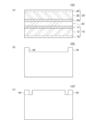
- (b) is a schematic top view thereof
- (c) is a schematic top view of another example of a light control film.
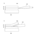
- FIG. It is an outline side view explaining an example of a peeling process of a substrate with a transparent electrode layer.
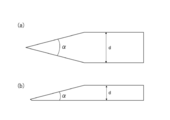
- FIG. 3 is a schematic top view illustrating an example of a step of peeling a substrate with a transparent electrode layer shown in FIG. 2. It is a schematic side view explaining the shape of a peeling means. It is the schematic explaining the positional relationship of a light control film and a peeling means. It is the schematic explaining an example of the removal process of the base material with a transparent electrode layer.
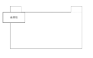
- FIG. 2 is a schematic top view of the light control film produced in Example 1.
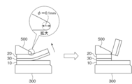
- FIG. 4 is a schematic diagram illustrating a peeling step in the first embodiment.
- FIG. 4 is a schematic diagram illustrating a peeling step in the first embodiment. It is the schematic explaining the measuring method of a crack bending diameter.
- the method for manufacturing a liquid crystal element having an extraction electrode portion includes: A first transparent electrode layer-attached base material and a second transparent electrode layer-attached substrate arranged such that the transparent electrode layers face each other, and a liquid crystal light modulating layer sandwiched between the transparent electrode layer-attached substrates.
- a light control film preparation step To obtain a light control film having an extending portion extending in a direction orthogonal to the thickness direction (a light control film preparation step);
- a peeling means is inserted between the transparent electrode layer-attached substrates, and one of the transparent electrode layer-attached substrates is peeled from the light control film (a step of peeling the transparent electrode layer-attached substrate).
- the manufacturing method may further include any additional steps as necessary. Hereinafter, each step will be described in detail.
- FIGS. 1A and 1B are a schematic cross-sectional view and a schematic top view, respectively, of an example of a light control film applicable to the present invention.
- FIG. 1C is a schematic top view of another example of the light control film applicable to the present invention.
- the light control film 100 includes a first base material 10 with a transparent electrode layer, a second base material 20 with a transparent electrode layer, and the base materials 10 and 20 with a transparent electrode layer. And a liquid crystal light control layer 30 interposed between the liquid crystal light control layers.
- the light control films 100 and 100 ' have an extension 40 extending in a direction orthogonal to the thickness direction.
- one of the base members with the transparent electrode layer is removed from the extension portion to expose the transparent electrode layer of the other base member with the transparent electrode layer.
- an extraction electrode portion is formed. Since one extraction electrode portion is usually provided for each transparent electrode layer, it is preferable that the light control film has two extending portions.
- a dimming element a device having an extraction electrode portion and capable of being connected to an external circuit
- a dimming film a device having no extraction electrode portion
- the first base material 10 with a transparent electrode layer includes a first transparent base material 12 and a first transparent base material 12 provided on one side thereof. It has a transparent electrode layer 14 and a first hard coat layer 16 provided on the other side.
- the first transparent electrode layer-attached base material 10 includes a first transparent base material 12 and a first transparent electrode layer, instead of the first hard coat layer 16 or in addition to the first hard coat layer 16. 14 may have a second hard coat layer (not shown). Further, the first substrate with a transparent electrode layer may have neither the first hard coat layer nor the second hard coat layer.
- the first substrate with a transparent electrode layer has a first hard coat layer, and more preferably has both a first hard coat layer and a second hard coat layer.
- an alignment film may be provided on the surface of the transparent electrode layer according to the drive mode.
- the crack bending diameter of the first transparent electrode layer-attached substrate is typically 0.1 mm to 5.0 mm, preferably 1.0 mm to 4.0 mm. Since the substrate with a transparent electrode layer having a crack bending diameter in the above range can be easily split at a desired position and removed, the extraction electrode portion can be formed without performing half-cut processing.
- the crack bending diameter means a minimum bending diameter that can be bent without generating a crack, and as shown in FIG. 11, in a U-shaped film bending test method, between parallel plates. The film is bent in a U-shape, and the distance between the plates is narrowed. This value is defined by the distance between the plates when the film breaks.
- the surface resistance of the substrate with the first transparent electrode layer is preferably from 0.1 ⁇ / ⁇ to 1000 ⁇ / ⁇ , more preferably from 0.5 ⁇ / ⁇ to 300 ⁇ / ⁇ , and still more preferably 1 ⁇ / ⁇ . ⁇ 200 ⁇ / ⁇ .
- the haze value of the substrate with the first transparent electrode layer is preferably 20% or less, more preferably 10% or less, and further preferably 0.1% to 10%.
- the total light transmittance of the substrate with the first transparent electrode layer is preferably 30% or more, more preferably 60% or more, and further preferably 80% or more.
- the first transparent electrode layer can be formed using, for example, a metal oxide such as indium tin oxide (ITO), zinc oxide (ZnO), and tin oxide (SnO 2 ).
- the metal oxide may be an amorphous metal oxide or a crystallized metal oxide.
- the first transparent electrode layer can be formed by a metal nanowire such as a silver nanowire (AgNW), a carbon nanotube (CNT), an organic conductive film, a metal layer, or a laminate thereof.
- the first transparent electrode layer can be patterned into a desired shape according to the purpose.
- the thickness of the first transparent electrode layer is preferably 0.01 ⁇ m to 0.10 ⁇ m, and more preferably 0.01 ⁇ m to 0.045 ⁇ m.
- the first transparent electrode layer is typically provided directly on one surface of the first transparent base material (if a hard coat layer is provided, the surface of the hard coat layer) using a method such as sputtering. .
- the first transparent substrate is formed of any appropriate material as long as a substrate with a transparent electrode layer having the above-mentioned crack bending diameter is obtained. Specifically, a glass substrate or a polymer substrate is preferably used.
- the above-mentioned polymer substrate is typically a polymer film mainly containing a thermoplastic resin.
- the thermoplastic resin include cycloolefin resins such as polynorbornene; acrylic resins; polyester resins; polycarbonate resins; and cellulose resins. Among them, a cycloolefin resin or an acrylic resin can be preferably used. Since these resin films have flexibility and relatively high brittleness at the same time, they can be easily broken by bending.
- the above thermoplastic resins may be used alone or in combination of two or more.
- the thickness of the first transparent substrate is preferably 20 ⁇ m to 200 ⁇ m, more preferably 30 ⁇ m to 100 ⁇ m.
- the first hard coat layer and the second hard coat layer provide the light control film with abrasion resistance and surface smoothness, and make the crack bending diameter of the first transparent electrode layer-attached substrate within the above range.
- Can contribute to The hard coat layer is, for example, a cured layer of any appropriate ultraviolet curable resin.
- the ultraviolet curable resin include an acrylic resin, a silicone resin, a polyester resin, a urethane resin, an amide resin, and an epoxy resin.
- the hard coat layer is formed by applying a coating liquid containing such a monomer or oligomer of an ultraviolet-curable resin and, if necessary, a photopolymerization initiator to the first transparent substrate, and drying the dried coating layer. By irradiating the substrate with ultraviolet rays to cure the substrate.
- the thickness of the hard coat layer is preferably 0.4 ⁇ m to 40 ⁇ m, more preferably 1 ⁇ m to 10 ⁇ m.
- the thickness of the hard coat layer is easily cracked at the time of bending, and the crack of the hard coat layer triggers the cracking of the transparent base material.
- the substrate can be cracked.
- the thickness of the hard coat layer (the total thickness when the first and second hard coat layers are formed) is 1% to 20%, preferably 2%, of the thickness of the first transparent substrate. % To 15%.
- the second substrate with a transparent electrode layer 20 includes a second transparent substrate 22 and a second transparent substrate 22 provided on one side thereof. It has a transparent electrode layer 24 and a third hard coat layer 26 provided on the other side.
- the second transparent electrode layer-attached base material 20 may be replaced with the third hard coat layer 26 or in addition to the third hard coat layer 26, and may include the second transparent base material 22 and the second transparent electrode layer 24, a fourth hard coat layer (not shown) may be provided.
- the second substrate with a transparent electrode layer may have neither the third hard coat layer nor the fourth hard coat layer.
- the substrate 20 with a second transparent electrode layer has a third hard coat layer, and more preferably has both a third hard coat layer and a fourth hard coat layer.
- an alignment film may be provided on the surface of the transparent electrode layer according to the drive mode.
- the crack bending diameter of the substrate with the second transparent electrode layer is typically from 0.1 mm to 5.0 mm, preferably from 1.0 mm to 4.0 mm.
- the substrate with a transparent electrode layer having a crack bending diameter in the above range can be easily split at a desired portion and removed, so that the extraction electrode portion can be formed without half cutting.
- the surface resistance of the second substrate with a transparent electrode layer is preferably from 0.1 ⁇ / ⁇ to 1000 ⁇ / ⁇ , more preferably from 0.5 ⁇ / ⁇ to 300 ⁇ / ⁇ , and still more preferably 1 ⁇ / ⁇ . ⁇ 200 ⁇ / ⁇ .
- the haze value of the substrate with the second transparent electrode layer is preferably 20% or less, more preferably 10% or less, and further preferably 0.1% to 10%.
- the total light transmittance of the substrate with the second transparent electrode layer is preferably 30% or more, more preferably 60% or more, and further preferably 80% or more.
- the second transparent electrode layer, the second transparent base material, the third hard coat layer, and the fourth hard coat layer are respectively the first transparent electrode layer, the first transparent base material, and the first hard base material.
- the same description as the coat layer and the second hard coat layer can be applied.
- the second substrate with a transparent electrode layer may have the same configuration as the first substrate with a transparent electrode layer, or may have a different configuration.
- the liquid crystal light control layer 30 typically has a structure in which a liquid crystal compound is dispersed in a resin matrix. Specific examples include a light control layer including a polymer dispersed liquid crystal, a light control layer including a polymer network liquid crystal, and the like.
- the polymer-dispersed liquid crystal has a structure in which liquid crystals are phase-separated in a polymer.
- the polymer network type liquid crystal has a structure in which a liquid crystal is dispersed in a polymer network, and the liquid crystal in the polymer network has a continuous phase.
- the peel strength at the interface between the liquid crystal light control layer and the substrate with a transparent electrode layer is relatively small.
- the peel strength at the interface between the liquid crystal light control layer and the substrate with the first transparent electrode layer is preferably 0.2 N / 25 mm to 5 N / 25 mm, and more preferably 0.6 N / 25 mm to 3 N / 25 mm.
- the peel strength at the interface between the liquid crystal light control layer and the substrate with the second transparent electrode layer is preferably 0.2 N / 25 mm to 5 N / 25 mm, more preferably 0.6 N / 25 mm to 3 N /. 25 mm.
- the adjustment of the peel strength can be performed by, for example, changing the viscosity and polarity of the resin matrix to change the adhesion and the adhesion to the base material with a transparent electrode layer (mainly, the transparent electrode layer). Specifically, by using a highly flexible resin matrix, using a non-polarized or low-polarized resin matrix by previously reacting a polar group such as a carboxyl group, by reducing the cohesive force of the resin matrix, and the like. Peel strength can be reduced.
- any suitable non-polymerized liquid crystal compound is used.
- nematic, smectic, and cholesteric liquid crystal compounds can be used. From the viewpoint of realizing excellent transparency in the transmission mode, it is preferable to use a nematic liquid crystal compound.
- the nematic liquid crystal compound include biphenyl compounds, phenylbenzoate compounds, cyclohexylbenzene compounds, azoxybenzene compounds, azobenzene compounds, azomethine compounds, terphenyl compounds, biphenylbenzoate compounds, and cyclohexylbiphenyl compounds.
- the content ratio of the liquid crystal compound in the liquid crystal light control layer is, for example, 10% by weight or more, preferably 30% by weight or more, more preferably 35% by weight or more, and further preferably 40% by weight or more.
- the content ratio is, for example, 90% by weight or less, preferably 70% by weight or less.
- the peel strength at the interface between the liquid crystal light control layer and the substrate with a transparent electrode layer can also be adjusted by the content ratio of the liquid crystal compound. When the content ratio of the liquid crystal compound is increased, the peeling strength can be reduced because the bonding area between the transparent electrode layer and the resin matrix decreases, and when the content ratio of the liquid crystal compound is reduced, the peel strength can be increased.
- the resin forming the resin matrix can be appropriately selected according to the light transmittance, the refractive index of the liquid crystal compound, the adhesion to the substrate with a transparent electrode layer, and the like.
- water-soluble resins or water-dispersible resins such as urethane resins, polyvinyl alcohol resins, polyethylene resins, polypropylene resins, and acrylic resins, and liquid crystal polymers, (meth) acrylic resins, silicone resins, and epoxy resins And a curable resin such as a fluorine resin, a polyester resin, and a polyimide resin.
- water-soluble or water-dispersible urethane resins and acrylic resins can be preferably used.
- the content ratio of the matrix forming resin in the liquid crystal light control layer is, for example, 90% by weight or less, preferably 70% by weight or less, more preferably 65% by weight or less, and further preferably 60% by weight or less.
- the content is, for example, 10% by weight or more, preferably 30% by weight or more.
- the thickness of the liquid crystal light control layer is preferably 30 ⁇ m or less, more preferably 20 ⁇ m or less, and still more preferably 15 ⁇ m or less.
- the lower limit of the thickness of the liquid crystal light control layer can be, for example, 5 ⁇ m. In the processing of a light control film having a liquid crystal light control layer having such a small thickness, the effects of the present invention can be particularly preferably obtained.
- the liquid crystal light control layer can be manufactured by any appropriate method.
- an emulsion method and a phase separation method can be given.
- the emulsion method it is easier to control the adhesion between the liquid crystal light control layer and the substrate provided with the transparent electrode layer than the phase separation method, so that it may be advantageous from the viewpoint of obtaining the above-mentioned preferable peel strength.
- the method for producing the liquid crystal light modulating layer of the emulsion method is, for example, by applying an emulsion coating liquid containing a matrix-forming resin and a liquid crystal compound to the transparent electrode layer surface of the first substrate with a transparent electrode layer. Forming a layer, and drying the coating layer to form a resin matrix on the matrix forming resin.
- the emulsion coating liquid is preferably an emulsion containing a liquid mixture of a matrix forming resin and a coating solvent in a continuous phase and a liquid crystal compound in a dispersed phase.
- a liquid crystal light modulating layer having a configuration in which a liquid crystal compound is dispersed in a resin matrix can be formed.
- a light control film is obtained by laminating a substrate with a second transparent electrode layer on a liquid crystal light control layer.
- extension portion 40 is a portion where the one substrate with a transparent electrode layer and the liquid crystal light control layer are removed to be an extraction electrode portion.
- the base material with the transparent electrode layer can be easily broken.
- the entire extension may be the extraction electrode, or a part of the extension may be the extraction electrode. In the case where the entire extension portion is used as the extraction electrode portion, one of the base materials with a transparent electrode layer is broken at the base portion (the portion indicated by a dotted line in the drawing) of the extension portion.
- the extension portion has a substantially rectangular shape in a top view, but is not limited to this shape, and may have any appropriate shape that can function as an extraction electrode portion.
- the light control film having the extension portion can be obtained, for example, by manufacturing or purchasing the long light control film and punching it into a corresponding shape.
- a peeling means is inserted between the transparent electrode layer-attached substrates in the extending portion, and one of the transparent electrode layer-attached substrates is removed. Peel from the light control film.
- the liquid crystal light control layer containing the dispersed liquid crystal compound has a smaller cohesive force than the base material with the transparent electrode layer, and preferably, the peel strength at the interface between the liquid crystal light control layer and the base material with the transparent electrode layer is set relatively small. Therefore, the peeling means can be easily inserted between the substrates with the transparent electrode layer, and as a result, the peeling of the substrate with the transparent electrode layer can be induced.
- FIGS. 2 and 3 are a schematic side view and a schematic top view, respectively, illustrating an example of a step of peeling the substrate with a transparent electrode layer.
- the light control film 100 is placed on the worktable 300, and the peeling means 200 is applied to the entire area of the extending portion 40 along the direction in which the base of the extending portion 40 (the line indicated by the dotted line in the drawing) extends. Is inserted. In the region where the peeling means is inserted, the substrate with the transparent electrode layer located above can be peeled from the light control film.
- the light control film is preferably fixed on a work table using a suction disk or the like.
- the shape of the peeling means 200 is not limited as long as it can be inserted between the transparent electrode layer-attached substrates and one of the transparent electrode layer-attached substrates can be peeled off.
- the peeling means is typically a thin plate-shaped member, preferably a thin plate-shaped blade member (for example, a razor blade-shaped blade member) having an edge on the side to be inserted.
- FIGS. 4A and 4B are schematic side views for explaining the shapes of the double-edged and single-edged peeling means, respectively.
- the cutting edge angle ⁇ may preferably be 10 ° to 40 °, more preferably 15 ° to 35 °, and even more preferably 20 ° to 30 °.
- the thickness d of the peeling means is preferably 50 ⁇ m to 1000 ⁇ m, more preferably 60 ⁇ m to 600 ⁇ m.
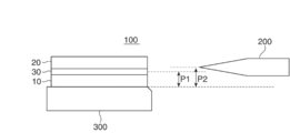
- FIG. 5 is a schematic diagram illustrating a positional relationship between the light control film and the peeling unit when the peeling unit is inserted.
- P1 the center height of the liquid crystal light control layer 30 in the light control film 100 placed on the worktable
- P2 ⁇ P1 is preferably ⁇ 100 ⁇ m or more.
- P2-P1 is preferably between -50 and 50. According to such a positional relationship, even when the thickness of the liquid crystal light control layer is small (for example, about 10 ⁇ m thick), it is possible to suitably insert the peeling means between the base materials with the transparent electrode layer and peel it. it can.
- the peeling means sandwiches the base material with a transparent electrode between the work table and the work table when inserted into the light control film. Therefore, it is preferable that the peeling means has elasticity so that the peeling means can be bent upward in response to stress.
- a peeling means can be formed using a metal such as stainless steel.
- the moving speed of the peeling means at the time of insertion can be preferably 1 mm / sec to 100 mm / sec, more preferably 2 mm / sec to 50 mm / sec, and still more preferably 3 mm / sec to 30 mm / sec.
- the insertion angle ⁇ 1 of the peeling means in the thickness direction of the light control film is, for example, ⁇ 30 ° to 30 °, preferably ⁇ 20 ° to 20 °, more preferably ⁇ with respect to a direction (horizontal direction) perpendicular to the thickness direction. It can be 10 ° to 10 °.
- the edge of the peeling means (preferably, the edge on which the blade is cut) and the edge of the extension are parallel to each other.
- the pressing may be performed, or the pressing may be performed at a non-parallel angle.
- the angle ⁇ 2 formed between the edge of the peeling means and the edge of the extension portion is, for example, 1 ° to 40 °, more specifically, 5 ° to 30 ° or 10 °. ° to 25 °.
- Step of Removing Substrate with Transparent Electrode Layer In the step of removing the substrate with transparent electrode layer, the peeled portion of the substrate with a transparent electrode layer is broken by bending it outward. In the present invention, since a substrate with a transparent electrode layer having a predetermined crack bending diameter is used, the peeled portion can be easily broken by the bending.
- FIG. 6 is a schematic view illustrating one embodiment of the step of removing the liquid crystal light control layer.
- the exfoliated portion of the transparent electrode layer-attached substrate is sandwiched by a gripper 400 having a substantially U-shaped cross section whose tip is sharper than the bent bending diameter of the substrate.
- the peeled portion of the second transparent electrode layer-attached substrate 20 is lifted upward.
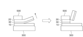
- FIG. 7 is a schematic view illustrating another embodiment of the step of removing the liquid crystal light control layer.
- the peeled portion is bent outward while the tip of the transparent electrode layer-attached base material that is not peeled off is pressed by a holding jig 500 whose tip is sharper than the bending bending diameter of the base material (FIG.
- the peeled portion of the substrate 20 with the second transparent electrode layer is lifted upward).
- the holding jig 500 the starting point of bending can be favorably controlled, and as a result, the substrate with a transparent electrode layer can be easily broken at a desired position.
- the transparent electrode layer in the corresponding portion of the other transparent electrode layer-containing substrate can be exposed. It can be used as an extraction electrode.
- the remaining liquid crystal light control layer is swollen or dissolved using a solvent capable of swelling or dissolving the liquid crystal light control layer. Then, it is removed by wiping with a rag or the like. Thereby, the transparent electrode layer of the other substrate with a transparent electrode layer can be exposed.
- solvents capable of dissolving the liquid crystal compound and dissolving or swelling the resin matrix for example, alcohols such as anhydrous ethanol, methanol, and isopropanol (IPA), and esters such as ethyl acetate and methyl acetate.
- alcohols such as anhydrous ethanol, methanol, and isopropanol (IPA)
- esters such as ethyl acetate and methyl acetate.
- ketones such as methyl ethyl ketone (MEK) and methyl isobutyl ketone (MIBK); waters such as alkaline washing water and pure water; or a mixed solvent thereof.
- MEK methyl ethyl ketone
- MIBK methyl isobutyl ketone
- the light control film preferably has two extending portions. Therefore, in one extension part, the peeling step and the removal step of one transparent electrode layer-attached base material are performed, and then, if necessary, the light control film is turned upside down, and in the other extension part, the other By performing the peeling step and the removing step of the substrate with a transparent electrode layer described above, it is possible to obtain a dimming element in which an extraction electrode portion is formed for each transparent electrode.
- the fracture bending diameter of the U-shaped film bending tester is such that the transparent electrode layer is located outside the transparent substrate between the two parallel plates and the transparent electrode layer-attached substrate is U-shaped.
- the board was bent and arranged, and the gap between the boards was reduced, and the gap between the boards when the substrate was cracked was measured.
- ⁇ Peel strength at the interface between the substrate with a transparent electrode layer and the liquid crystal light control layer was determined according to JIS K 6854-3: 1999. At a speed of 300 mm / min in a direction of 180 °, and the peeling stress was measured.
- Example 1 Preparation of light control film (preparation of first and second transparent electrode layer substrates) Corona treatment was performed on both surfaces of a cycloolefin-based transparent substrate (Norbornene-based resin film, product name “ZF-16”, thickness: 40 ⁇ m, Re [590]: 5 nm, manufactured by Zeon Corporation). Thereafter, a coating solution consisting of 49 parts of trifunctional acrylic PETA, 1 part of an initiator (Irgacure 907) and 50 parts of ethyl acetate is applied to each surface, and after drying the ethyl acetate, high-pressure mercury UV is irradiated at 300 mJ / m 2.
- a coating solution consisting of 49 parts of trifunctional acrylic PETA, 1 part of an initiator (Irgacure 907) and 50 parts of ethyl acetate is applied to each surface, and after drying the ethyl acetate, high-pressure mercury UV is irradiated at 300 mJ /
- a hard coat layer having a thickness of 2 ⁇ m was formed.
- an ITO layer having a thickness of 25 nm was formed on one surface by a sputtering method, and annealed at 140 ° C. for 1 hour to form an ITO crystal film (transparent electrode layer) of 100 ⁇ / ⁇ .
- the first and second substrates with a transparent electrode layer having the configuration of [hard coat layer / cycloolefin-based transparent substrate / hard coat layer / transparent electrode layer] were obtained.
- the crack bending diameter of the obtained first and second substrates with a transparent electrode layer was 2 mm.
- the second substrate with a transparent electrode layer was laminated on the liquid crystal light control layer such that the transparent electrode layer faced the liquid crystal light control layer to obtain a light control film.
- the obtained light control film was punched out with a Thomson blade to obtain a light control film having two extended portions as shown in FIG.
- the peel strength at the interface between the liquid crystal light control layer and the substrate with a transparent electrode layer in the light control film was measured, the peel strength was 0.9 N / 25 mm, and the liquid crystal light control layer and the second transparent electrode were separated. Peeled between layers with the layered substrate.
- Step of peeling off the second transparent electrode layer-attached substrate The light control film having the above-mentioned extended portion was placed on an adsorption table and fixed so that the first transparent electrode layer-attached substrate was on the lower side.
- the peeling means a stainless steel thin plate (blade angle 22 °, thickness 120 ⁇ m) having one blade on one end is used, and the height of the blade tip of the peeling means coincides with the center height of the liquid crystal light control layer. And the angle ⁇ 2 between the edged edge of the peeling means and the edge of the extension was set to 20 °. From this state, as shown in FIG. 2 and FIG. 3, when the peeling means was horizontally moved toward the light control film at a speed of 5 mm / sec. It entered along the layer between the liquid crystal light control layer. By moving the peeling means so as to trace the entire area of the extending portion, the substrate with the second transparent electrode layer in the area was peeled from the light control film.
- the tip of the second transparent electrode layer-attached substrate is held down along the base of the extension (at a position 20 mm from the tip of the extension) as a holding jig.
- the tip of the peeled second transparent electrode layer-attached base material was pushed upward with a finger in a 45 ° direction while applying a sharp stainless steel metal plate having a diameter of 0.1 mm.
- the substrate with a transparent electrode layer was cracked, thereby exposing the liquid crystal light control layer.
- Step of removing and removing the substrate with the first transparent electrode layer The light control film is turned upside down and placed on an adsorption table to be fixed, and the same as in the step of removing and removing the substrate with the second transparent electrode layer. Then, when the first substrate with a transparent electrode layer in the other extension was split, the liquid crystal light control layer did not remain on the second substrate with a transparent electrode layer, and the ITO electrode surface was exposed. I was
- Example 1 In the same manner as in Example 1, a light control film having two extending portions as shown in FIG. 8 was obtained. The obtained light control film was placed and fixed on an adsorption table such that the substrate with the first transparent electrode layer was on the lower side. The surface of the light control film (specifically, the surface of the base material with the second transparent electrode layer) is irradiated with a carbon dioxide gas laser so as to trace the base portion of the extension portion (the line indicated by the dotted line in the figure). When cut processing was performed, the liquid crystal light control layer began to be deformed by heating as compared with the second transparent electrode layer-attached base material, so that the half cut could not be performed.
- Example 2 In the same manner as in Example 1, a light control film having two extending portions as shown in FIG. 8 was obtained. The obtained light control film was placed and fixed on an adsorption table such that the substrate with the first transparent electrode layer was on the lower side. By tracing the base portion of the extension portion (the line indicated by the dotted line in the figure) using a half-cutter (a single-cut cutter product name “Kirinook 209B”) with respect to one extension portion, Half cut processing for cutting the base material with the transparent electrode layer 2 was performed.
- a half-cutter a single-cut cutter product name “Kirinook 209B”
- the base material with the second transparent electrode layer was cut only halfway, and was half cut. Did not. With respect to the remaining 18 light control films, the cut pieces of the substrate with the second transparent electrode layer were peeled off, and the liquid crystal light control layer was exposed. Anhydrous ethanol was dropped on the exposed portion of the liquid crystal light modulating layer to swell, and then wiped off with a rag to expose the ITO electrode surface of the first transparent electrode layer-attached base material to form an extraction electrode portion.
- the 18 light control films are turned upside down, placed on an adsorption table and fixed, and the other extension is subjected to a half-cut process for cutting the first transparent electrode layer-attached base material in the same manner as described above.
- the first substrate with a transparent electrode layer was cut only halfway, and was not half-cut.
- the cut pieces of the substrate with the first transparent electrode layer were peeled off, and the liquid crystal light control layer did not remain on the substrate with the second transparent electrode layer. The electrode surface was exposed.
- a conduction test was performed by applying a sine wave voltage of an effective voltage of 50 V (60 Hz) to the 20 light control elements obtained in Example 1. As a result, it was confirmed that all the dimming elements changed to the transmission mode, and the energizing operation was performed. On the other hand, a sine wave voltage of an effective voltage of 50 V (60 Hz) was applied to the 17 dimming elements obtained in Comparative Example 2 to perform a conduction test. As a result, it was confirmed that 15 light modulating elements changed to the transmission mode and the energizing operation was performed. However, the haze did not change and the energizing operation was not confirmed for the two light modulating elements. An analysis was performed on the two light control elements that did not conduct electricity, and it was found that the first transparent electrode layer was disconnected.
- the manufacturing method of the present invention is suitable for manufacturing a light control device having a liquid crystal light control layer.
- this is advantageous when the thickness of the liquid crystal light control layer is small and it is difficult to stably form the extraction electrode portion by half-cutting using a laser or a half-cutter.
Landscapes
- Physics & Mathematics (AREA)
- Nonlinear Science (AREA)
- Chemical & Material Sciences (AREA)
- Optics & Photonics (AREA)
- Crystallography & Structural Chemistry (AREA)
- General Physics & Mathematics (AREA)
- Mathematical Physics (AREA)
- Dispersion Chemistry (AREA)
- Geometry (AREA)
- Liquid Crystal (AREA)
- Electroluminescent Light Sources (AREA)
- Chemical And Physical Treatments For Wood And The Like (AREA)
- Cereal-Derived Products (AREA)
Abstract
Description
1つの実施形態において、上記調光フィルムが、第1の延出部および第2の延出部を有し、上記製造方法が、該第1の延出部において、上記透明電極層付基材間に剥離手段を挿入して、一方の透明電極層付基材を上記調光フィルムから剥離すること、該一方の透明電極層付基材の剥離部分を外方に折り曲げて折り割ること、該第2の延出部において、上記透明電極層付基材間に剥離手段を挿入して、他方の透明電極層付基材を上記調光フィルムから剥離すること、および、該他方の透明電極層付基材の剥離部分を外方に折り曲げて折り割ること、を含み、上記第1の透明電極層付基材および第2の透明電極層付基材の割れ屈曲直径が、0.1mm~5mmである。
1つの実施形態において、上記第1の透明電極層付基材と上記液晶調光層との界面および/または上記第2の透明電極層付基材と上記液晶調光層との界面の剥離強度が、0.2N/25mm~5N/25mmである。
1つの実施形態において、上記第1の透明電極層付基材および/または上記第2の透明電極層付基材が、透明基材と該透明基材の一方の側に設けられた透明電極層とを有し、該透明基材の形成材料が、ガラス、シクロオレフィン系樹脂およびアクリル系樹脂から選択される少なくとも1種を含む。
1つの実施形態において、上記第1の透明電極層付基材および/または上記第2の透明電極層付基材が、透明基材と、該透明基材の一方の側に設けられた透明電極層と、該透明基材の他方の側に設けられたハードコート層とを有する。
1つの実施形態において、上記第1の透明電極層付基材および/または上記第2の透明電極層付基材が、透明基材と、該透明基材の一方の側に設けられた透明電極層と、該透明基材の他方の側および該透明基材と該透明電極層との間に設けられたハードコート層とを有する。
1つの実施形態において、上記液晶調光層の厚みが、15μm以下である。
透明電極層同士が対向するように配置された第1の透明電極層付基材および第2の透明電極層付基材と該透明電極層付基材間に挟持された液晶調光層とを有し、厚み方向と直交する方向に延出した延出部を有する、調光フィルムを得ること(調光フィルムの準備工程)、
該延出部において、該透明電極層付基材間に剥離手段を挿入して、一方の透明電極層付基材を該調光フィルムから剥離すること(透明電極層付基材の剥離工程)、および
該一方の透明電極層付基材の剥離部分を外方に折り曲げて折り割ること(透明電極層付基材の除去工程)、を含む。当該製造方法は、必要に応じて、任意の付加的な工程をさらに含んでもよい。以下、各工程について詳細に説明する。
図1(a)および(b)はそれぞれ、本発明に適用可能な調光フィルムの一例の概略断面図および概略上面図である。また、図1(c)は、本発明に適用可能な調光フィルムの別の例の概略上面図である。図1(a)に示されるとおり、調光フィルム100は、第1の透明電極層付基材10および第2の透明電極層付基材20と、該透明電極層付基材10と20との間に挟持された液晶調光層30と、を有する。また、図1(b)、(c)に示されるとおり、調光フィルム100、100’は、厚み方向と直交する方向に延出した延出部40を有する。本発明の製造方法においては、当該延出部において一方の透明電極層付基材を除去して他方の透明電極層付基材の透明電極層を露出させる。これにより、取出し電極部が形成される。取出し電極部は、通常、各透明電極層に対して1つずつ設けられることから、調光フィルムは、2つの延出部を有することが好ましい。なお、本明細書において、取出し電極部を有し、外部回路との接続が可能であるものを調光素子と称し、取出し電極部が形成されていない状態のものを調光フィルムと称する場合がある。
図1(a)に示されるとおり、第1の透明電極層付基材10は、第1の透明基材12とその一方の側に設けられた第1の透明電極層14と、他方の側に設けられた第1のハードコート層16とを有する。第1の透明電極層付基材10は、第1のハードコート層16に代えて、あるいは、第1のハードコート層16に加えて、第1の透明基材12と第1の透明電極層14との間に第2のハードコート層(図示せず)を有するものであってもよい。また、第1の透明電極層付基材は、第1のハードコート層および第2のハードコート層のいずれをも有さないものであり得る。好ましくは、第1の透明電極層付基材は、第1のハードコート層を有し、より好ましくは第1のハードコート層および第2のハードコート層の両方を有する。また、図示しないが、駆動モードに応じて、透明電極層表面に配向膜が設けられてもよい。
図1(a)に示されるとおり、第2の透明電極層付基材20は、第2の透明基材22とその一方の側に設けられた第2の透明電極層24と、他方の側に設けられた第3のハードコート層26とを有する。第2の透明電極層付基材20は、第3のハードコート層26に代えて、あるいは、第3のハードコート層26に加えて、第2の透明基材22と第2の透明電極層24との間に第4のハードコート層(図示せず)を有するものであってもよい。また、第2の透明電極層付基材は、第3のハードコート層および第4のハードコート層のいずれをも有さないものであり得る。好ましくは、第2の透明電極層付基材20は、第3のハードコート層を有し、より好ましくは第3のハードコート層と第4のハードコート層の両方を有する。また、図示しないが、駆動モードに応じて、透明電極層表面に配向膜が設けられてもよい。
液晶調光層30は、代表的には、樹脂マトリクス中に液晶化合物が分散した構造を有する。具体例としては、高分子分散型液晶を含む調光層、高分子ネットワーク型液晶を含む調光層等が挙げられる。高分子分散型液晶は、高分子内において液晶が相分離した構造を有している。高分子ネットワーク型液晶は、高分子ネットワーク中に液晶が分散された構造を有しており、高分子ネットワーク中の液晶は、連続相を有している。
延出部40は、一方の透明電極層付基材および液晶調光層が除去されて、取出し電極部とされる部分である。調光機能を発揮する調光部本体と一辺においてのみ接続するように延出部を設けることにより、簡便に透明電極層付基材を折り割ることができる。延出部全域が取出し電極部とされてもよく、延出部の一部が取出し電極部とされてもよい。延出部全域が取出し電極部とされる場合、延出部の付け根部分(図中、点線で示される部分)で一方の透明電極層付基材が折り割られる。
透明電極層付基材の剥離工程においては、延出部において、透明電極層付基材間に剥離手段を挿入して、一方の透明電極層付基材を調光フィルムから剥離する。分散した液晶化合物を含む液晶調光層は透明電極層付基材よりも凝集力が小さく、また、好ましくは液晶調光層-透明電極層付基材界面の剥離強度が比較的小さく設定されることから、剥離手段が透明電極層付基材間に容易に挿入され得、その結果として、透明電極層付基材の剥離が誘導され得る。
透明電極層付基材の除去工程においては、上記透明電極層付基材の剥離部分を外方に折り曲げることによって折り割る。本発明においては、所定の割れ屈曲直径を有する透明電極層付基材が用いられることから、当該折り曲げによって簡便に剥離部分を折り割ることができる。
割れ屈曲直径は、U字型フィルム屈曲試験機において、図11に示すように平行な2枚の板の間に透明基材よりも透明電極層を外側にして透明電極層付基材をU字状に屈曲させて配置し、その板の間隔を狭くしていき、基材が割れるときの板の間隔を測定した。
≪透明電極層付基材と液晶調光層との界面の剥離強度≫
透明電極層付基材と液晶調光層との界面の剥離強度は、JIS K 6854-3:1999接着強さ試験方法に従って25mm幅の短冊状の試験片に剥離のきっかけを作った後、室温にて、300mm/分の速さで180°の方向にピールし、その剥離応力を測定した。
1.調光フィルムの準備工程
(第1および第2の透明電極層付基材の作製)
シクロオレフィン系透明基材(日本ゼオン社製、ノルボルネン系樹脂フィルム、製品名「ZF-16」、厚み:40μm、Re[590]:5nm)の両面にコロナ処理を行った。その後、各々の面に3官能アクリルPETA49部、開始剤(Irgacure907)1部、酢酸エチル50部からなる塗工液を塗布し、酢酸エチルを乾燥後、高圧水銀UVを300mJ/m2照射することにより、2μm厚のハードコート層を形成した。さらに、一方の面に、スパッタ法により25nm厚のITO層を形成し、140℃で1時間アニールして、100Ω/□のITO結晶膜(透明電極層)を形成した。このようにして、[ハードコート層/シクロオレフィン系透明基材/ハードコート層/透明電極層]の構成を有する第1および第2の透明電極層付基材を得た。得られた第1および第2の透明電極層付基材の割れ屈曲直径は、2mmであった。
下記の組成の化合物を150℃で20分混合し、その後室温に徐冷するにより、Δn=0.12、粘度=21cP、Δε=10.1、液晶温度=3~52℃の液晶化合物(1)を得た。

ウレタンエマルション溶液(楠本化成社製、製品名「NeoRez R967」)50部(固形分)に、液晶化合物(1) 50部を添加し、ホモジナイザーで攪拌することにより、液晶化合物の液滴(平均粒径:5μm)を含むエマルション塗工液を得た。エマルション塗工液を第1の透明電極層付基材の透明電極層側表面に塗布および乾燥させ、これにより、12μm厚の液晶調光層を形成した。
液晶調光層上に、透明電極層が液晶調光層に対向するように第2の透明電極層付基材を積層して、調光フィルムを得た。次いで、得られた調光フィルムをトムソン刃で打ち抜くことにより、図8に示すような2つの延出部を有する調光フィルムを得た。なお、当該調光フィルムにおける液晶調光層と透明電極層付基材との界面の剥離強度を測定したところ、剥離強度は0.9N/25mmであり、液晶調光層と第2の透明電極層付基材との層間で剥離した。
上記延出部を有する調光フィルムを第1の透明電極層付基材が下側となるように吸着台に載せて固定した。剥離手段として、1つの端辺に両刃が刃付けされたステンレス製の薄板(刃先角度22°、厚み120μm)を用い、該剥離手段の刃先先端の高さと液晶調光層の中心高さとが一致するように、かつ、剥離手段の刃付けされた端辺と延出部の端辺とのなす角度θ2が20°となるようにセットした。当該状態から、図2および図3に示すように、剥離手段を5mm/秒の速度で調光フィルムに向かって水平移動させたところ、該剥離手段は、第2の透明電極層付基材と液晶調光層との層間に沿って進入した。当該延出部全域をなぞるように該剥離手段を移動させることにより、当該領域の第2の透明電極層付基材を調光フィルムから剥離した。
図9、図10に示すように、延出部の付け根に沿うように(延出部の先端から20mmの位置に)、押さえ冶具として、先端が直径0.1mmの鋭利なステンレス金属板をあてながら、剥離した第2の透明電極層付基材の先端を指で上方に45度の方向に押し上げたところ、金属板の先端で容易に第2の透明電極層付基材が割れ、これにより、液晶調光層が露出した。
調光フィルムを上下反転させて吸着台に乗せて固定し、上記第2の透明電極層付基材の剥離工程および除去工程と同様にして、他方の延出部における第1の透明電極層付基材を割ったところ、液晶調光層は第2の透明電極層付基材上に残留しておらず、ITO電極面が露出していた。
実施例1と同様にして、図8に示すような2つの延出部を有する調光フィルムを得た。得られた調光フィルムを第1の透明電極層付基材が下側となるように吸着台に載せて固定した。延出部の付け根部分(図中の点線で示すライン)をなぞるように調光フィルム表面(具体的には、第2の透明電極層付基材表面)に炭酸ガスレーザーを照射して、ハーフカット加工したところ、第2の透明電極層付基材よりも液晶調光層が加熱変形し始めたために、ハーフカットができなかった。
実施例1と同様にして、図8に示すような2つの延出部を有する調光フィルムを得た。得られた調光フィルムを第1の透明電極層付基材が下側となるように吸着台に載せて固定した。一方の延出部に関して、ハーフカッター(オルファ社製、一枚切カッター製品名「キリヌーク209B」)を用いて延出部の付け根部分(図中の点線で示すライン)上をなぞることにより、第2の透明電極層付基材を切断するハーフカット加工を行った。
実施例1で得た20枚の調光素子に対して、実効電圧50V(60Hz)の正弦波電圧を印加して通電検査を行った。その結果、全ての調光素子が透過モードに変化し、通電動作することが確認できた。一方、比較例2で得た17枚の調光素子に対して、実効電圧50V(60Hz)の正弦波電圧を印加して通電検査を行った。その結果、15枚の調光素子が透過モードに変化し、通電動作することが確認できたが、2枚の調光素子はヘイズが変化せず、通電動作が確認できなかった。通電動作しなかった2枚の調光素子について分析を行ったところ、第1の透明電極層が断線していた。
12 第1の透明基材
14 第1の透明電極層
16 第1のハードコート層
20 第2の透明電極層付基材
22 第2の透明基材
24 第2の透明電極層
26 第3のハードコート層
30 液晶調光層
100 調光フィルム
200 剥離手段
Claims (7)
- 透明電極層同士が対向するように配置された第1の透明電極層付基材および第2の透明電極層付基材と該透明電極層付基材間に挟持された液晶調光層とを有し、厚み方向と直交する方向に延出した延出部を有する、調光フィルムを得ること、
該延出部において、該透明電極層付基材間に剥離手段を挿入して、一方の透明電極層付基材を該調光フィルムから剥離すること、および、
該一方の透明電極層付基材の剥離部分を外方に折り曲げて折り割ること、を含み、
該一方の透明電極層付基材の割れ屈曲直径が、0.1mm~5mmである、
取出し電極部を有する調光素子の製造方法。 - 前記調光フィルムが、第1の延出部および第2の延出部を有し、
該第1の延出部において、前記透明電極層付基材間に剥離手段を挿入して、一方の透明電極層付基材を前記調光フィルムから剥離すること、
該一方の透明電極層付基材の剥離部分を外方に折り曲げて折り割ること、
該第2の延出部において、前記透明電極層付基材間に剥離手段を挿入して、他方の透明電極層付基材を前記調光フィルムから剥離すること、および
該他方の透明電極層付基材の剥離部分を外方に折り曲げて折り割ること、を含み、
前記第1の透明電極層付基材および第2の透明電極層付基材の割れ屈曲直径が、0.1mm~5mmである、請求項1に記載の製造方法。 - 前記第1の透明電極層付基材と前記液晶調光層との界面および/または前記第2の透明電極層付基材と前記液晶調光層との界面の剥離強度が、0.2N/25mm~5N/25mmである、請求項1または2に記載の製造方法。
- 前記第1の透明電極層付基材および/または前記第2の透明電極層付基材が、透明基材と該透明基材の一方の側に設けられた透明電極層とを有し、
該透明基材の形成材料が、ガラス、シクロオレフィン系樹脂およびアクリル系樹脂から選択される少なくとも1種を含む、請求項1から3のいずれかに記載の製造方法。 - 前記第1の透明電極層付基材および/または前記第2の透明電極層付基材が、透明基材と、該透明基材の一方の側に設けられた透明電極層と、該透明基材の他方の側に設けられたハードコート層とを有する、請求項1から4のいずれかに記載の製造方法。
- 前記第1の透明電極層付基材および/または前記第2の透明電極層付基材が、透明基材と、該透明基材の一方の側に設けられた透明電極層と、該透明基材の他方の側および該透明基材と該透明電極層との間に設けられたハードコート層とを有する、請求項1から5のいずれかに記載の製造方法。
- 前記液晶調光層の厚みが、15μm以下である、請求項1から6のいずれかに記載の製造方法。
Priority Applications (4)
| Application Number | Priority Date | Filing Date | Title |
|---|---|---|---|
| JP2020546849A JP7322046B2 (ja) | 2018-09-10 | 2019-08-29 | 調光素子の製造方法 |
| US17/274,967 US12050385B2 (en) | 2018-09-10 | 2019-08-29 | Method for manufacturing dimming element |
| CN201980057537.2A CN112639593B (zh) | 2018-09-10 | 2019-08-29 | 调光元件的制造方法 |
| KR1020217006884A KR102721282B1 (ko) | 2018-09-10 | 2019-08-29 | 조광 소자의 제조 방법 |
Applications Claiming Priority (2)
| Application Number | Priority Date | Filing Date | Title |
|---|---|---|---|
| JP2018168728 | 2018-09-10 | ||
| JP2018-168728 | 2018-09-10 |
Publications (1)
| Publication Number | Publication Date |
|---|---|
| WO2020054445A1 true WO2020054445A1 (ja) | 2020-03-19 |
Family
ID=69778269
Family Applications (1)
| Application Number | Title | Priority Date | Filing Date |
|---|---|---|---|
| PCT/JP2019/033909 Ceased WO2020054445A1 (ja) | 2018-09-10 | 2019-08-29 | 調光素子の製造方法 |
Country Status (6)
| Country | Link |
|---|---|
| US (1) | US12050385B2 (ja) |
| JP (1) | JP7322046B2 (ja) |
| KR (1) | KR102721282B1 (ja) |
| CN (1) | CN112639593B (ja) |
| TW (1) | TWI820202B (ja) |
| WO (1) | WO2020054445A1 (ja) |
Cited By (8)
| Publication number | Priority date | Publication date | Assignee | Title |
|---|---|---|---|---|
| KR20210065954A (ko) * | 2018-10-04 | 2021-06-04 | 닛토덴코 가부시키가이샤 | 조광 소자의 제조 방법 |
| JP2022069915A (ja) * | 2020-10-26 | 2022-05-12 | 凸版印刷株式会社 | 配向膜付き透明導電フィルム、調光フィルム、調光板および調光装置 |
| EP4036640A4 (en) * | 2020-12-14 | 2022-12-07 | Shanghai Longsheng Photoelectric New Material Co., Ltd. | METHOD OF MANUFACTURING A PDLC MEMBRANE ELECTRODE, A VACUUM PLATFORM AND A PDLC MEMBRANE |
| JP2023074433A (ja) * | 2021-11-17 | 2023-05-29 | 凸版印刷株式会社 | 調光シート |
| JP2023074431A (ja) * | 2021-11-17 | 2023-05-29 | 凸版印刷株式会社 | 調光シート |
| JP2023074432A (ja) * | 2021-11-17 | 2023-05-29 | 凸版印刷株式会社 | 調光シート |
| WO2023219061A1 (ja) * | 2022-05-11 | 2023-11-16 | 凸版印刷株式会社 | 調光シート、および調光シートの製造方法 |
| EP4361710A4 (en) * | 2021-07-01 | 2024-12-11 | Fuyao Glass Industry Group Co., Ltd. | DIMMING COMPONENT AND MANUFACTURING METHOD THEREOF, LIGHT TRANSMISSION ASSEMBLY AND VEHICLE |
Families Citing this family (2)
| Publication number | Priority date | Publication date | Assignee | Title |
|---|---|---|---|---|
| WO2023192117A1 (en) | 2022-03-29 | 2023-10-05 | Nitto Denko Corporation | Polymer matrix with mesogenic ligand and light shutter including the same |
| JP2025170989A (ja) * | 2024-05-08 | 2025-11-20 | Toppanホールディングス株式会社 | 調光シート、調光装置、および調光シートの製造方法 |
Citations (4)
| Publication number | Priority date | Publication date | Assignee | Title |
|---|---|---|---|---|
| JPH035135U (ja) * | 1989-05-31 | 1991-01-18 | ||
| JPH04126224U (ja) * | 1991-04-30 | 1992-11-17 | タキロン株式会社 | 調光パネル |
| JP2011232626A (ja) * | 2010-04-28 | 2011-11-17 | Seiko Electric Co Ltd | 調光素子及び調光構造体 |
| KR20160109465A (ko) * | 2015-03-11 | 2016-09-21 | (주)베스트룸 | 고분자 분산형 액정표시장치 |
Family Cites Families (11)
| Publication number | Priority date | Publication date | Assignee | Title |
|---|---|---|---|---|
| JP3619058B2 (ja) * | 1998-06-18 | 2005-02-09 | キヤノン株式会社 | 半導体薄膜の製造方法 |
| TW558743B (en) * | 2001-08-22 | 2003-10-21 | Semiconductor Energy Lab | Peeling method and method of manufacturing semiconductor device |
| US7307778B2 (en) * | 2002-04-24 | 2007-12-11 | Sipix Imaging, Inc. | Compositions and processes for format-flexible, roll-to-roll manufacturing of electrophoretic displays |
| TWI430435B (zh) | 2006-09-29 | 2014-03-11 | 半導體能源研究所股份有限公司 | 半導體裝置的製造方法 |
| JP2008225397A (ja) | 2007-03-16 | 2008-09-25 | Citizen Holdings Co Ltd | 液晶表示素子の製造方法 |
| JP2008225398A (ja) | 2007-03-16 | 2008-09-25 | Citizen Holdings Co Ltd | 液晶表示素子の製造方法 |
| WO2011132327A1 (ja) | 2010-04-22 | 2011-10-27 | 株式会社正興電機製作所 | 封止テープ、調光素子、調光構造体及び調光構造体の製造方法 |
| TWI618131B (zh) | 2013-08-30 | 2018-03-11 | 半導體能源研究所股份有限公司 | 剝離起點形成裝置及形成方法、疊層體製造裝置 |
| KR102165162B1 (ko) * | 2014-03-12 | 2020-10-14 | 삼성디스플레이 주식회사 | 기판 박리 장치 및 이를 이용한 소자 제조 방법 |
| JP2018116273A (ja) | 2017-01-13 | 2018-07-26 | 日東電工株式会社 | 光学積層体 |
| EP3570094B1 (en) | 2017-01-13 | 2022-06-22 | Nitto Denko Corporation | Light control film |
-
2019
- 2019-08-29 US US17/274,967 patent/US12050385B2/en active Active
- 2019-08-29 JP JP2020546849A patent/JP7322046B2/ja active Active
- 2019-08-29 WO PCT/JP2019/033909 patent/WO2020054445A1/ja not_active Ceased
- 2019-08-29 CN CN201980057537.2A patent/CN112639593B/zh active Active
- 2019-08-29 KR KR1020217006884A patent/KR102721282B1/ko active Active
- 2019-09-06 TW TW108132190A patent/TWI820202B/zh active
Patent Citations (4)
| Publication number | Priority date | Publication date | Assignee | Title |
|---|---|---|---|---|
| JPH035135U (ja) * | 1989-05-31 | 1991-01-18 | ||
| JPH04126224U (ja) * | 1991-04-30 | 1992-11-17 | タキロン株式会社 | 調光パネル |
| JP2011232626A (ja) * | 2010-04-28 | 2011-11-17 | Seiko Electric Co Ltd | 調光素子及び調光構造体 |
| KR20160109465A (ko) * | 2015-03-11 | 2016-09-21 | (주)베스트룸 | 고분자 분산형 액정표시장치 |
Cited By (14)
| Publication number | Priority date | Publication date | Assignee | Title |
|---|---|---|---|---|
| KR20210065954A (ko) * | 2018-10-04 | 2021-06-04 | 닛토덴코 가부시키가이샤 | 조광 소자의 제조 방법 |
| KR102785433B1 (ko) * | 2018-10-04 | 2025-03-21 | 닛토덴코 가부시키가이샤 | 조광 소자의 제조 방법 |
| JP2022069915A (ja) * | 2020-10-26 | 2022-05-12 | 凸版印刷株式会社 | 配向膜付き透明導電フィルム、調光フィルム、調光板および調光装置 |
| JP7619001B2 (ja) | 2020-10-26 | 2025-01-22 | Toppanホールディングス株式会社 | 調光フィルム、調光板および調光装置 |
| EP4036640A4 (en) * | 2020-12-14 | 2022-12-07 | Shanghai Longsheng Photoelectric New Material Co., Ltd. | METHOD OF MANUFACTURING A PDLC MEMBRANE ELECTRODE, A VACUUM PLATFORM AND A PDLC MEMBRANE |
| US12253767B2 (en) | 2020-12-14 | 2025-03-18 | Shanghai Longsheng Photoelectric New Material Co., Ltd. | Method for manufacturing PDLC membrane electrode, negative pressure platform and PDLC membrane |
| EP4361710A4 (en) * | 2021-07-01 | 2024-12-11 | Fuyao Glass Industry Group Co., Ltd. | DIMMING COMPONENT AND MANUFACTURING METHOD THEREOF, LIGHT TRANSMISSION ASSEMBLY AND VEHICLE |
| JP2023074433A (ja) * | 2021-11-17 | 2023-05-29 | 凸版印刷株式会社 | 調光シート |
| JP2023074432A (ja) * | 2021-11-17 | 2023-05-29 | 凸版印刷株式会社 | 調光シート |
| JP2023074431A (ja) * | 2021-11-17 | 2023-05-29 | 凸版印刷株式会社 | 調光シート |
| JP7753826B2 (ja) | 2021-11-17 | 2025-10-15 | Toppanホールディングス株式会社 | 調光シート |
| JP7753825B2 (ja) | 2021-11-17 | 2025-10-15 | Toppanホールディングス株式会社 | 調光シート |
| JP7753824B2 (ja) | 2021-11-17 | 2025-10-15 | Toppanホールディングス株式会社 | 調光シート |
| WO2023219061A1 (ja) * | 2022-05-11 | 2023-11-16 | 凸版印刷株式会社 | 調光シート、および調光シートの製造方法 |
Also Published As
| Publication number | Publication date |
|---|---|
| JP7322046B2 (ja) | 2023-08-07 |
| KR102721282B1 (ko) | 2024-10-23 |
| CN112639593A (zh) | 2021-04-09 |
| JPWO2020054445A1 (ja) | 2021-08-30 |
| US12050385B2 (en) | 2024-07-30 |
| US20220035197A1 (en) | 2022-02-03 |
| KR20210043610A (ko) | 2021-04-21 |
| CN112639593B (zh) | 2024-09-24 |
| TWI820202B (zh) | 2023-11-01 |
| TW202020529A (zh) | 2020-06-01 |
Similar Documents
| Publication | Publication Date | Title |
|---|---|---|
| JP7322046B2 (ja) | 調光素子の製造方法 | |
| CN102282485B (zh) | 偏光板的制造方法 | |
| EP3051391A1 (en) | Touch panel | |
| CN101486202A (zh) | 层叠体的切断方法及在该方法中采用的切刀 | |
| JP4918064B2 (ja) | 積層体の切断方法 | |
| CN106992139B (zh) | 一种柔性显示面板的制造方法 | |
| WO2021010114A1 (ja) | 光学積層体およびその製造方法 | |
| JP2000105669A (ja) | タッチ入力方式の液晶ディスプレイ装置及びその製造方法 | |
| JP6065142B1 (ja) | 調光フィルム、合わせガラス及び調光フィルムの製造方法 | |
| JP7047724B2 (ja) | 調光セル、調光体及び移動体 | |
| KR102795679B1 (ko) | 표면 보호 필름 부착 봉지 조광 소자 | |
| JP2013047157A (ja) | 積層中間膜およびその製造方法、ならびに、合わせガラスおよびその製造方法 | |
| JP7326733B2 (ja) | 調光フィルム、調光装置 | |
| JP2023003753A (ja) | 光学積層体及び表示装置 | |
| JP7796191B1 (ja) | 三次元曲面部を有する調光フィルムおよびその製造方法 | |
| JP7779152B2 (ja) | 液晶セル、液晶装置 | |
| JP5828815B2 (ja) | 積層中間膜およびその製造方法、ならびに、合わせガラスおよびその製造方法 | |
| JP2019191480A (ja) | 調光フィルム | |
| JP7279346B2 (ja) | 調光フィルム、調光装置 | |
| JP2004302476A5 (ja) | ||
| WO2026048398A1 (ja) | 調光フィルム | |
| JP2004240455A (ja) | タッチ入力方式の液晶ディスプレイ装置 | |
| JP2023135820A (ja) | 調光シート及び調光シートの製造方法 | |
| JP2004302476A (ja) | タッチ入力方式の液晶ディスプレイ装置の製造方法 | |
| JP2004227010A (ja) | タッチ入力方式の液晶ディスプレイ装置 |
Legal Events
| Date | Code | Title | Description |
|---|---|---|---|
| 121 | Ep: the epo has been informed by wipo that ep was designated in this application |
Ref document number: 19859080 Country of ref document: EP Kind code of ref document: A1 |
|
| ENP | Entry into the national phase |
Ref document number: 2020546849 Country of ref document: JP Kind code of ref document: A |
|
| ENP | Entry into the national phase |
Ref document number: 20217006884 Country of ref document: KR Kind code of ref document: A |
|
| NENP | Non-entry into the national phase |
Ref country code: DE |
|
| 122 | Ep: pct application non-entry in european phase |
Ref document number: 19859080 Country of ref document: EP Kind code of ref document: A1 |