WO2020054096A1 - Led駆動装置、照明装置、および車載用表示装置 - Google Patents
Led駆動装置、照明装置、および車載用表示装置 Download PDFInfo
- Publication number
- WO2020054096A1 WO2020054096A1 PCT/JP2019/006482 JP2019006482W WO2020054096A1 WO 2020054096 A1 WO2020054096 A1 WO 2020054096A1 JP 2019006482 W JP2019006482 W JP 2019006482W WO 2020054096 A1 WO2020054096 A1 WO 2020054096A1
- Authority
- WO
- WIPO (PCT)
- Prior art keywords
- led
- current
- voltage
- driving device
- terminal
- Prior art date
- Legal status (The legal status is an assumption and is not a legal conclusion. Google has not performed a legal analysis and makes no representation as to the accuracy of the status listed.)
- Ceased
Links
Images












Classifications
-
- H—ELECTRICITY
- H05—ELECTRIC TECHNIQUES NOT OTHERWISE PROVIDED FOR
- H05B—ELECTRIC HEATING; ELECTRIC LIGHT SOURCES NOT OTHERWISE PROVIDED FOR; CIRCUIT ARRANGEMENTS FOR ELECTRIC LIGHT SOURCES, IN GENERAL
- H05B45/00—Circuit arrangements for operating light-emitting diodes [LED]
- H05B45/30—Driver circuits
- H05B45/32—Pulse-control circuits
- H05B45/325—Pulse-width modulation [PWM]
-
- B—PERFORMING OPERATIONS; TRANSPORTING
- B60—VEHICLES IN GENERAL
- B60Q—ARRANGEMENT OF SIGNALLING OR LIGHTING DEVICES, THE MOUNTING OR SUPPORTING THEREOF OR CIRCUITS THEREFOR, FOR VEHICLES IN GENERAL
- B60Q3/00—Arrangement of lighting devices for vehicle interiors; Lighting devices specially adapted for vehicle interiors
- B60Q3/10—Arrangement of lighting devices for vehicle interiors; Lighting devices specially adapted for vehicle interiors for dashboards
- B60Q3/16—Circuits; Control arrangements
- B60Q3/18—Circuits; Control arrangements for varying the light intensity
-
- H—ELECTRICITY
- H05—ELECTRIC TECHNIQUES NOT OTHERWISE PROVIDED FOR
- H05B—ELECTRIC HEATING; ELECTRIC LIGHT SOURCES NOT OTHERWISE PROVIDED FOR; CIRCUIT ARRANGEMENTS FOR ELECTRIC LIGHT SOURCES, IN GENERAL
- H05B45/00—Circuit arrangements for operating light-emitting diodes [LED]
- H05B45/10—Controlling the intensity of the light
-
- H—ELECTRICITY
- H05—ELECTRIC TECHNIQUES NOT OTHERWISE PROVIDED FOR
- H05B—ELECTRIC HEATING; ELECTRIC LIGHT SOURCES NOT OTHERWISE PROVIDED FOR; CIRCUIT ARRANGEMENTS FOR ELECTRIC LIGHT SOURCES, IN GENERAL
- H05B45/00—Circuit arrangements for operating light-emitting diodes [LED]
- H05B45/30—Driver circuits
- H05B45/345—Current stabilisation; Maintaining constant current
-
- H—ELECTRICITY
- H05—ELECTRIC TECHNIQUES NOT OTHERWISE PROVIDED FOR
- H05B—ELECTRIC HEATING; ELECTRIC LIGHT SOURCES NOT OTHERWISE PROVIDED FOR; CIRCUIT ARRANGEMENTS FOR ELECTRIC LIGHT SOURCES, IN GENERAL
- H05B45/00—Circuit arrangements for operating light-emitting diodes [LED]
- H05B45/30—Driver circuits
- H05B45/37—Converter circuits
- H05B45/3725—Switched mode power supply [SMPS]
-
- H—ELECTRICITY
- H05—ELECTRIC TECHNIQUES NOT OTHERWISE PROVIDED FOR
- H05B—ELECTRIC HEATING; ELECTRIC LIGHT SOURCES NOT OTHERWISE PROVIDED FOR; CIRCUIT ARRANGEMENTS FOR ELECTRIC LIGHT SOURCES, IN GENERAL
- H05B45/00—Circuit arrangements for operating light-emitting diodes [LED]
- H05B45/50—Circuit arrangements for operating light-emitting diodes [LED] responsive to malfunctions or undesirable behaviour of LEDs; responsive to LED life; Protective circuits
- H05B45/56—Circuit arrangements for operating light-emitting diodes [LED] responsive to malfunctions or undesirable behaviour of LEDs; responsive to LED life; Protective circuits involving measures to prevent abnormal temperature of the LEDs
-
- Y—GENERAL TAGGING OF NEW TECHNOLOGICAL DEVELOPMENTS; GENERAL TAGGING OF CROSS-SECTIONAL TECHNOLOGIES SPANNING OVER SEVERAL SECTIONS OF THE IPC; TECHNICAL SUBJECTS COVERED BY FORMER USPC CROSS-REFERENCE ART COLLECTIONS [XRACs] AND DIGESTS
- Y02—TECHNOLOGIES OR APPLICATIONS FOR MITIGATION OR ADAPTATION AGAINST CLIMATE CHANGE
- Y02B—CLIMATE CHANGE MITIGATION TECHNOLOGIES RELATED TO BUILDINGS, e.g. HOUSING, HOUSE APPLIANCES OR RELATED END-USER APPLICATIONS
- Y02B20/00—Energy efficient lighting technologies, e.g. halogen lamps or gas discharge lamps
- Y02B20/30—Semiconductor lamps, e.g. solid state lamps [SSL] light emitting diodes [LED] or organic LED [OLED]
Definitions
- the present invention relates to an LED driving device.
- LEDs light emitting diodes
- Patent Document 1 A conventional example of an LED driving device that drives an LED is disclosed in Patent Document 1.
- the LED driving device of Patent Document 1 has a DC / DC controller that controls an output stage for generating an output voltage from an input voltage and supplying the output voltage to the LED, and a constant current driver that generates an output current flowing to the LED. Then, a plurality of systems of LEDs are driven.
- the DC / DC controller includes an error amplifier that compares the lowest voltage among the cathode voltages of the plurality of LEDs with a reference voltage, a PWM comparator that compares an output of the error amplifier with a slope signal and generates an internal PWM signal.
- the constant current driver is turned on and off based on an external PWM signal input to the PWM terminal. As a result, PWM dimming control is performed. While the constant current driver is on, the switching element in the output stage is PWM-driven by the switching pulse by the error amplifier and the PWM comparator such that the minimum voltage of the cathode voltage matches the reference voltage. As a result, the output voltage (the anode voltage of the LED) is controlled to a voltage value obtained by adding the reference voltage to the maximum voltage among the forward voltages of the LEDs of the plural systems.
- an object of the present invention is to provide an LED driving device capable of increasing the dimming rate of PWM dimming.
- the LED driving device includes: A DC / DC controller for controlling an output stage for generating an output voltage from an input voltage and supplying the output voltage to the LED; A current driver for generating an output current of the LED; Has, The current driver turns on the output current in accordance with the LED current on period of the PWM dimming signal, and turns off the output current in accordance with the LED current off period of the PWM dimming signal, thereby performing PWM dimming.
- the DC / DC controller comprises: A feedback control unit that performs feedback control to output a switching pulse to the output stage so that a cathode voltage of the LED matches a reference voltage; A pulse addition control unit that performs pulse addition control for adding a predetermined number of additional switching pulses when switching between the LED current on period and the LED current off period; Has, The predetermined number of pulses is variably set.
- the dimming rate of PWM dimming can be increased.
- FIG. 1 is a circuit configuration diagram showing a configuration of an LED driving device according to an embodiment of the present invention.
- 9 is a timing chart as a comparative example for the pulse addition control.
- 6 is a timing chart illustrating an example of pulse addition control.
- 9 is a graph illustrating an example of a relationship between a PWM dimming on-duty and an output current according to a comparative example.
- 9 is a graph illustrating an example of a relationship between a PWM dimming on-duty and an output current when pulse addition control is performed.
- 6 is a timing chart showing a detailed waveform example at the time of pulse addition control.
- 6 is a timing chart showing a detailed waveform example at the time of pulse addition control.
- FIG. 9 is a diagram illustrating a configuration example for setting the number of additional switching pulses.
- 9 is a table showing an example of a relationship between a combination of resistance values and a set number of pulses.
- 9 is a timing chart illustrating a waveform example at the time of pulse addition control according to a first modification.
- 11 is a timing chart illustrating a waveform example during pulse addition control according to a second modification.
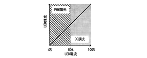
- FIG. 9 is a diagram illustrating a part of a configuration of an LED driving device according to a first modification. It is a graph which shows the dimming switching when LED current ratio threshold is set to 50%. It is a graph which shows dimming switching when LED current ratio threshold is 25%. It is a graph which shows dimming switching when the LED current ratio threshold value is set to 100%.
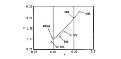
- 5 is a graph illustrating an example of a relationship between LED current and LED luminosity. 5 is a graph illustrating an example of a relationship between LED current and chromaticity. It is a figure showing a part of composition of an LED drive device concerning a 2nd modification. 5 is a timing chart illustrating an example of delay control of LED current on / off timing. It is a package top view of the LED drive device concerning a 2nd modification.
- FIG. 3 is a plan view showing an arrangement of electrode pads and an arrangement of each region where each circuit block is arranged on the chip.
- FIG. 3 is a diagram illustrating a configuration example of a backlight device. It is a figure showing an example of an in-vehicle display.
- FIG. 1 is a circuit configuration diagram showing a configuration of an LED driving device 30 according to one embodiment of the present invention.
- the LED driving device 30 shown in FIG. 1 drives a plurality of (six in this embodiment) LED arrays 41 to 46.
- the LED driving device 30 includes an internal voltage generator 1, a current detector 2, a charge pump 3, an oscillator 4, a slope generator 5, a spectrum spreader 6, a PWM comparator 7, a control logic unit 8,
- This is a semiconductor device having an integrated current driver 18, LED current setting unit 19, reference voltage source 20, and Schmitt trigger 21.
- the LED driving device 30 includes a VCC terminal, a VREG terminal, a CSH terminal, an SD terminal, a CPP terminal, a CPM terminal, a CP terminal, a BOOT terminal, an OUTH terminal as external terminals for establishing an electrical connection with the outside.
- An output stage 35 for generating an output voltage Vout from the input voltage Vin by DC / DC conversion and supplying the output voltage Vout to the LED arrays 41 to 46 is arranged outside the LED driving device 30.
- the output stage 35 has a capacitor Cvcc, a resistor Rsh, a switching element N1, a diode D1, an inductor L1, a diode D2, a switching element N2, an output capacitor Co, and a capacitor Cbt.
- the switching elements N1 and N2 are driven and controlled by the LED driving device 30, the output stage 35 is controlled by the LED driving device 30.
- the output stage 35 and the LED driving device 30 form a DC / DC converter.
- a step-up / step-down DC / DC converter is particularly configured as the DC / DC converter.
- the application terminal of the input voltage Vin is connected to one end of the capacitor Cvcc.
- the other end of the capacitor Cvcc is connected to a ground terminal.
- the application end of the input voltage Vin is connected to one end of the resistor Rsh.
- the other end of the resistor Rsh is connected to the source of the transistor M1 including a p-channel MOSFET.
- the drain of the transistor M1 is connected to the drain of the switching element N1 composed of an n-channel MOSFET.
- the source of the switching element N1 is connected to the cathode of the diode D1.
- the anode of the diode D1 is connected to the ground terminal.
- the gate of the switching element N1 is connected to the OUTH terminal.
- One end of the inductor L1 is connected to a node where the switching element N1 and the diode D1 are connected.
- the other end of the inductor L1 is connected to the drain of the switching element N2 formed of an n-channel MOSFET together with the anode of the diode D2.
- the source of the switching element N2 is connected to the ground terminal via the resistor Rsl.
- the gate of the switching element N2 is connected to the OUTL terminal.
- the cathode of the diode D2 is connected to one end of the output capacitor Co.
- the other end of the output capacitor Co is connected to a ground terminal.
- An output voltage Vout is generated at one end of the output capacitor Co.
- a bootstrap capacitor Cbt is connected to the node where the switching element N1 and the diode D1 are connected together with the SW terminal.
- the other end of the capacitor Cbt is connected to a BOOT terminal.
- the switching element N1 and the switching element N2 may be included in the LED driving device.
- Each anode of the LED arrays 41 to 46 is connected to one end of the output capacitor Co where the output voltage Vout is generated.
- Each of the LED arrays 41 to 46 includes a plurality of LEDs connected in series. The cathodes of the LED arrays 41 to 46 are connected to the LED1 to LED6 terminals, respectively.
- the LED arrays 41 to 46 are not limited to being connected in series, but may be composed of, for example, LEDs connected in series or parallel, or may be composed of only one LED.
- the number of drivable LED arrays is not limited to six, but may be four, for example. Alternatively, only one LED array may be driven.
- the internal voltage generator 1 When the EN terminal is high, the internal voltage generator 1 generates an internal voltage Vreg (for example, 5 V) from the input voltage Vin applied to the VCC terminal, and outputs the generated internal voltage Vreg from the VREG terminal.
- the internal voltage Vreg is used as a power supply voltage of an internal circuit included in the LED driving device 30.
- the capacitor Cvg is connected to the VREG terminal.
- the charge pump 3 is connected to a CPP terminal, a CPM terminal, and a CP terminal.
- a charge pump capacitor Ccp1 is connected between the CPP terminal and the CPM terminal.
- a capacitor Ccp2 is connected to a CP terminal, which is an output terminal of the charge pump 3.
- the charge pump 3 boosts the input internal voltage Vreg and outputs it from the CP terminal.
- the oscillation unit 4 generates a predetermined clock signal according to the input signal to the SYNC terminal or the terminal voltage of the RT terminal, and outputs this to the slope generation unit 5.
- the slope generation unit 5 generates a slope signal (triangular wave signal) Vslp based on the clock signal input from the oscillation unit 4, and outputs this to the PWM comparator 7. Further, the current detection unit 2 has a function of giving an offset to the slope signal Vslp according to the CSL terminal voltage obtained by converting the current flowing through the switching element N2 by the resistor Rsl.
- the LED driving device 30 includes a SYNC terminal for receiving a clock input for externally synchronizing the step-up / step-down DC / D converter.
- the oscillation frequency of the DC / DC converter can be arbitrarily and highly precisely variably controlled using the RT terminal or the SYNC terminal.
- the LED drive device 30 when used as the backlight control means of the vehicle-mounted display device, if the external synchronous oscillation frequency is appropriately set from the SYNC terminal in accordance with the switching control of the radio reception frequency, the oscillation frequency of the DC / DC converter Can be avoided from overlapping with the frequency band of the radio noise, so that the backlight control can be performed without deteriorating the radio reception quality.
- the spread spectrum unit 6 can reduce the average of noise by changing the switching frequency of the DC / DC converter. ON / OFF of the spread spectrum unit 6 is switched by a SYNC terminal.
- the PWM comparator 7 generates an internal PWM signal by comparing the error signal Verr input to the non-inverting input terminal (+) with the slope signal Vslp input to the inverting input terminal (-), and generates an internal PWM signal. Output to the unit 8.
- the control logic unit 8 generates drive signals for the upper driver 9, the transistor 10, and the lower driver 11 based on the internal PWM signal.
- the upper driver 9 drives the OUTH terminal voltage (gate voltage of the switching element N1) between the BOOT terminal voltage and the SW terminal voltage based on the drive signal input from the control logic unit 8.
- the switching element N1 is turned on / off based on a gate voltage input from the upper driver 9.
- the switching element 10 is turned on / off based on the drive signal input from the control logic unit 8, and conducts / cuts off between the SW terminal and the ground terminal.
- the lower driver 11 pulse-drives the gate voltage of the switching element N2 between the output voltage CP of the charge pump 3 and the ground voltage based on the drive signal input from the control logic unit 8.
- the switching element N2 is turned on / off based on a gate voltage input from the lower driver 11.
- LED LED terminal voltages Vled1 to Vled6 are applied to the LED1 terminal to LED6 terminal as cathode voltages of the LED arrays 41 to 46, respectively.
- the selector 16 selects the lowest voltage among the LED terminal voltages Vled1 to Vled6 and outputs the same to one inverting input terminal (-) of the error amplifier 15.
- An OVP terminal voltage obtained by dividing the output voltage Vout by the voltage dividing resistors Rovp1 and Ropv2 is applied to the other inverting input terminal ( ⁇ ) of the error amplifier 15.
- the reference voltage Vref is applied to the non-inverting input terminal (+) of the error amplifier 15.
- the error amplifier 15 generates an error signal Verr by amplifying the difference between the lower voltage of the voltages applied to the two inverting input terminals ( ⁇ ) and the reference voltage Vref, and outputs the error signal Verr to the PWM comparator 7. I do.
- the feedback control based on the OVP terminal is performed only at the time of startup to accelerate the startup, and the feedback control based on the output of the selector 16 is performed after the startup.
- the output terminal of the error amplifier 15 is connected to the COMP terminal.
- the COMP terminal is connected to a ground terminal via a resistor Rpc and a capacitor Cpc that are externally connected in series.
- the soft start unit 13 controls the voltage level of the error signal Verr to gradually increase. As a result, overshoot and inrush current of the output voltage Vout can be suppressed.
- the protection circuit unit 17 includes a TSD unit (overheat protection circuit), an OCP unit, an OVP unit, an LED open detection circuit (OPEN), an LED short detection circuit (SHORT), an output short circuit protection circuit (SCP), A UVLO unit.
- TSD unit overheat protection circuit
- OCP unit OCP unit
- OVP unit OCP unit
- OPEN LED open detection circuit
- SHORT LED short detection circuit
- SCP output short circuit protection circuit
- a UVLO unit A UVLO unit.
- the TSD unit shuts down circuits other than the internal voltage generation unit 1 when the junction temperature of the LED driving device 30 becomes, for example, 175 ° C. or higher.
- the TSD unit returns the circuit operation when the junction temperature of the LED driving device 30 becomes, for example, 150 ° C.
- the current detection unit 2 monitors a CSH terminal voltage (input current detection voltage) in which a current flowing through the switching element N1 is detected as a voltage signal by the resistor Rsh, and when the CSH terminal voltage becomes, for example, Vin-0.6 V or less. Instructs the OCP unit to apply overcurrent protection. The OCP unit turns off DC / DC switching when applying overcurrent protection.
- CSH terminal voltage input current detection voltage
- the gate of the transistor M1 is connected to the SD terminal.
- the current detection unit 2 turns off the transistor M1 and cuts off the path from the application terminal of the input voltage Vin to the inductor L1.
- the OVP section monitors the OVP terminal voltage and applies overvoltage protection when the OVP terminal voltage becomes, for example, 2.0 V or more. When overvoltage protection is applied, DC / DC switching is turned off.
- LED open detection circuit when any one of the LED terminal voltages Vled1 to Vled6 is, for example, 0.3 V or less and the OVP terminal voltage is, for example, 2.0 V or more, LED open detection is performed and the open detection is performed. Only the LED array that is turned off is latched off.
- LED short detection circuit SHORT
- a resistor Rsht for setting LED short protection is connected to the SHT terminal.
- the output short-circuit protection circuit (SCP) is built in when the OVP terminal voltage becomes, for example, 0.57 V or less, or when any of the LED terminal voltages Vled1 to Vled6 becomes, for example, 0.3V or less.
- the counter operation is started, and after about 100 ms (FOSC: 300 kHz) elapses, latching is performed, and circuits other than the internal voltage generator 1 are shut down.
- the output short-circuit protection circuit is used for ground fault protection when the anode side (DC / DC output end side) of the LED arrays 41 to 46 is grounded or when the cathode side of the LED arrays 41 to 46 is grounded. Yes, it is.
- the UVLO unit shuts down circuits other than the internal voltage generation unit 1 when the input voltage Vin becomes, for example, 3.5 V or less, or when the internal voltage Vreg becomes, for example, 2.0 V or less.
- the protection circuit section 17 outputs an abnormality detection signal from the FAIL1 terminal to the outside based on the abnormality detection state of the OVP section and the OCP section.
- the VREG terminal is connected to the FAIL1 terminal via the resistor Rf1.
- the protection circuit unit 17 turns on a transistor (not shown) connected to the FAIL1 terminal, thereby setting the FAIL1 terminal to Low output.
- the protection circuit section 17 outputs an abnormality detection signal from the FAIL2 terminal to the outside based on the abnormality detection state of the LED open detection circuit, the LED short detection circuit, and the output short circuit protection circuit (SCP).
- the VREG terminal is connected to the FAIL2 terminal via the resistor Rf2.
- the protection circuit unit 17 turns on a transistor (not shown) connected to the FAIL2 terminal. As a result, the FAIL2 terminal is set to Low output.
- the Schmitt trigger 21 transmits a PWM dimming signal input from the outside to the PWM terminal to the constant current driver 18.
- the PWM dimming signal is input as a pulse signal.
- the LED current setting unit 19 sets a constant current value corresponding to the resistance value of the resistor Riset connected to the ISET terminal in the constant current driver 18.
- the reference voltage source 20 generates a reference voltage Vref.
- the constant current driver 18 has a constant current circuit 181 for six systems arranged between each of the LED1 to LED6 terminals and the LGND terminal connected to the ground terminal.
- the constant current driver 18 further has a PWM control logic unit 182.
- the PWM control logic unit 182 controls on / off of the constant current circuit 181 according to the on-duty of the PWM dimming indicated by the PWM dimming signal. Specifically, the constant current circuit 181 is turned on during the LED current on period according to the on-duty of the PWM dimming, and the constant current circuit 181 is turned off during the LED current off period according to the on-duty of the PWM dimming.
- the constant current circuit 181 is on, the output current ILED having the constant current value set by the LED current setting unit 19 flows.
- the VDISC terminal is connected to the output discharge unit 14.
- the VDISC terminal is connected to one end of an output capacitor Co that generates an output voltage Vout. If the operation is started in a state where the charge remains in the output capacitor Co, the LED may flicker. Therefore, it is necessary to discharge the output capacitor Co at the time of start-up. However, it may take time to discharge the charge only by the discharge paths such as the resistors Rovp1 and Rovp2 for setting the OVP. Discharge residual charges. The discharging is performed when the DC / DC converter is off (when the signal applied to the EN terminal falls or is protected).
- the GND terminal is a terminal for applying the GND of the small signal block inside the LED driving device 30.
- DC / DC controller 301 (the oscillation unit 4, the slope generation unit 5, the PWM comparator 7, the control logic unit 8, the upper driver 9, the transistor 10, the lower driver 11, and the error amplifier 15 of the LED driving device 30) Circuit block).
- the error amplifier 15 generates an error voltage Verr by amplifying a difference between the lowest value of the LED terminal voltages Vled1 to Vled6 selected by the selector 16 and the lower voltage of the OVP terminal voltage and the reference voltage Vref. .
- the voltage value of the error voltage Verr becomes higher as the lower voltage is lower than the reference voltage Vref.
- the PWM comparator 7 compares the error voltage Verr with the slope signal Vslp to generate an internal PWM signal.
- the internal PWM signal goes to a high level when the error voltage Verr is higher than the slope signal Vslp, and goes to a low level when the error voltage Verr is lower than the slope signal Vslp.
- the control logic unit 8 performs on / off control of the switching element N1, the transistor 10, and the switching element N2 based on the internal PWM signal. More specifically, the control logic unit 8 turns on the switching elements N1 and N2 and turns off the transistor 10 when the internal PWM signal is at a high level. Conversely, when the internal PWM signal is at a low level, the control logic unit 8 turns off the switching elements N1 and N2 and turns on the transistor 10.
- the feedback control unit including the error amplifier 15, the PWM comparator 7, the control logic unit 8, the upper driver 9, and the lower driver 11 performs switching so that the minimum value of the LED terminal voltages Vled1 to Vled6 matches the reference voltage Vref.
- the LED arrays 41 to 46 are supplied with the output voltage Vout obtained by raising and lowering the input voltage Vin.
- the step-down operation of the input voltage Vin is performed, and the duty ratio of the switching element N1 is smaller than 50%. If it is larger, the boosting operation of the input voltage Vin is performed.
- the LED drive device 30 it is possible to easily and appropriately switch the step-up / step-down operation while having a simple configuration.
- the LED driving device 30 can always obtain a desired output voltage Vout regardless of whether the input voltage Vin is higher or lower than the desired output voltage Vout.
- the desired value of the output voltage Vout is 16 V
- the desired output voltage Vout can be obtained even when the input voltage Vin varies in the range of 6 to 18 V.
- Such a configuration is suitable, for example, for an application (for example, an LED driver IC for backlight control of a car navigation monitor) that needs to correspond to an input voltage Vin directly supplied from a battery.
- the LED driving device 30 has the transistor 10 as a ringing preventing means under light load or no load. It is desirable that the current capability of the transistor 10 be designed to a minimum necessary for extracting a small current called ringing noise so as not to cause an unnecessary increase in chip area and a decrease in conversion efficiency.
- the switching of the transistor 10 is controlled to be complementary (exclusive) with the switching elements N1 and N2.
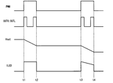
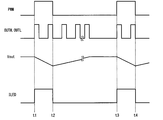
- FIG. 2 is a timing chart as a comparative example for the pulse addition control, and shows a PWM dimming signal, a switching pulse output from the OUTH and OUTL terminals, an output voltage Vout, and an output current ILED from the upper stage.
- PWM dimming signal High (ON level) indicates LED current ON and Low (OFF level) indicates LED current OFF.
- the constant current circuit 181 turns on the output current ILED by the PWM control logic unit 182.
- the LED terminal voltages Vled1 to Vled6 drop sharply due to the forward voltages of the LED arrays 41 to 46, and the DC / DC controller 301 operates the error amplifier 15 and the PWM comparator 7 to switch the switching pulses from the OUTH and OUT terminals.
- the constant current circuit 181 turns off the output current ILED by the PWM control logic unit 182.
- the LED terminal voltages Vled1 to Vled6 rise sharply, and the switching pulses from the OUTH and OUTL terminals by the DC / DC controller 301 are stopped at the off level.
- the output voltage Vout decreases due to the LED load by the LED arrays 41 to 46. This is because at the start of switching pulse output, the current flowing through the inductor L1 rises from zero and energy is gradually stored in the inductor L1, but at the same time, an LED load is generated. As shown in FIG. 2, when the on-duty of the PWM dimming is very low and the period between the timings t1 and t2 is short, the switching pulse is insufficient and the output current ILED is turned off at the timing t2 when the output voltage Vout is decreasing. And the output voltage Vout is maintained.
- the control logic unit 8 (that is, the DC / DC controller 301) switches the PWM dimming from the LED current ON period to the LED current OFF period at timing t2. , OUTH and OUTL terminals, and outputs a predetermined number of switching pulses. That is, the control logic unit 8 corresponds to a pulse addition control unit that performs pulse addition control.
- the output capacitor Co is charged after switching to the LED current OFF, and the output voltage Vout increases.
- the output current ILED does not become unstable.
- the output voltage Vout reduced during the LED current ON period is supplemented by the added switching pulse, so that the output voltage Vout can be held, and the output current ILED is stabilized.
- the lighting of the LED can be performed normally.
- the DC / DC controller 301 retains and uses the duty of the last switching pulse in the immediately preceding LED current ON period (t1 to t2) as the duty of the additional switching pulse. Further, the DC / DC controller 301 uses the duty of the last switching pulse in the previous LED current ON period (t1 to t2) as the switching pulse when the LED current ON period (t3 to t4) starts.
- FIG. 4 is a graph showing an example of the relationship between the PWM dimming on-duty and the output current ILED when the control without adding the switching pulse as shown in FIG. 2 is used.
- the PWM dimming on-duty becomes lower than around 0.1%, the amount of decrease in the output current ILED increases.
- FIG. 5 is a graph showing an example of the relationship between the PWM dimming on-duty and the output current ILED when the pulse addition control for adding the switching pulse as shown in FIG. 3 of the present embodiment is performed.
- FIG. 5 in contrast to FIG. 4, even when the PWM dimming on-duty is lower than around 0.1%, the amount of decrease in the output current ILED can be suppressed. That is, in the example shown in FIG. 5, it is possible to cope with the PWM dimming on-duty of 100% to 0.01%, and the dimming rate becomes 10000 times, thereby realizing the harmonic dimming rate. .
- the above-described pulse addition control is desirably performed in the entire range from the lower limit (for example, 0.01%) to the upper limit (for example, 100%) of the PWM dimming on-duty.
- the PWM dimming on-duty when the PWM dimming on-duty is switched, it is possible to avoid that the control mode is switched and the luminance becomes unstable due to a decrease in the LED current.
- the PWM dimming on-duty is high, the output voltage Vout may be sufficiently maintained during the LED current ON period. In such a case, for example, only when the PWM dimming on-duty is lower than a predetermined threshold, Pulse addition control may be performed.
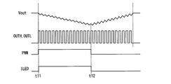
- FIG. 6 is a timing chart illustrating an example of the above-described pulse addition control, and includes an output voltage Vout, a switching pulse output from the OUTH and OUTL terminals from the upper stage, a PWM dimming signal, and an output current flowing through the LED. 3 shows an ILED. FIG. 6 shows a more specific waveform than FIG. 3 described above.
- FIG. 6 shows a case where the PWM dimming on-duty is low, that is, a case where the LED current-on period, which is a period from timing t11 to t12, is short, and a switching pulse is output in this period.
- the output voltage Vout decreases.
- a switching pulse having 12 pulses is added. Thereby, the output voltage Vout is supplemented.
- FIG. 7 is a view corresponding to FIG. 6, but shows a case where the LED load is lighter than that of FIG. In this case, the amount of decrease in the output voltage Vout during the LED current ON period, which is the period from timing t11 to t12, is suppressed. In such a case, if 12 switching pulses are added similarly to FIG. 6, the output voltage Vout is excessively supplemented. As a result, there is a possibility that the ripple generated in the output voltage Vout becomes large. When the ripple increases, the noise generated in the output capacitor Co may increase.
- the number of additional pulses is variably set. Specifically, in FIG. 7, the LED load is lighter than in FIG. 6, and the amount of decrease in the output voltage Vout during the LED current ON period is suppressed. A switching pulse has been added. Thereby, the supplement of the output voltage Vout by the additional pulse becomes appropriate. Therefore, the ripple generated in the output voltage Vout can be suppressed, and the noise of the output capacitor Co can be suppressed.
- the control logic unit 8 changes the number of added switching pulses. For example, if the LED driving device 30 is for a backlight of a vehicle-mounted display device, the LED load changes according to the display size of the vehicle-mounted display device.
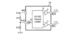
- the control logic unit 8 varies the number of additional pulses using the PLSET terminal. More specifically, as shown in FIG. 8, resistors R11 and R12 are connected in series between a VREG terminal and a ground terminal, and a PLSET terminal is connected to a connection node between the resistors R11 and R12. The voltage applied to the PLSET terminal is input to the control logic unit 8 via the Schmitt trigger 12. The division ratio of the internal voltage Vreg generated at the VREG terminal changes according to the combination of the resistance values of the resistors R11 and R12, and the voltage applied to the PLSET terminal changes. Therefore, the control logic unit 12 varies the number of additional pulses output from the OUTH and OUTL terminals according to the voltage applied to the PLSET terminal.
- FIG. 9 is a table showing an example of the relationship between the combination of the resistance values of the resistors R11 and R12 and the number of additional pulses.
- the number of additional pulses is variably set to 0, 4, 8, 12, or 16 according to the combination of the resistance values of the resistors R11 and R12.
- the voltage divided by the resistors R11 and R12 is used as the internal voltage Vreg because a comparator that compares the voltage applied to the PLSET terminal with a reference voltage is provided inside the control logic unit 8. This is because it is based on the internal voltage Vreg. That is, even when the internal voltage Vreg fluctuates, the reference voltage also fluctuates, so that an erroneous determination of the threshold value of the voltage applied to the PLSET terminal can be avoided, and an erroneous setting of the number of additional pulses can be avoided.
- the Schmitt trigger 12 has a function of preventing an indefinite signal when a voltage near the threshold of the comparator is applied to the PLSET terminal.
- the number of additional pulses is not limited to being set by a resistor, but may be set by, for example, a capacitance value of an external capacitor or a register.
- FIG. 10 is a timing chart showing an example of the switching pulse addition control according to the first modification, and is a diagram corresponding to FIG.
- the output current ILED flowing through the LED is turned on during a period from t22 to t23 when the PWM dimming signal is on level.
- a switching pulse is added in a period from t21 to t22 immediately before the PWM dimming signal is switched to the ON level.
- the output voltage Vout that decreases during the LED current ON period is compensated by the added switching pulse, so that the output voltage Vout can be held.
- the output current ILED can be stabilized, and the LED can be normally lit.
- the energy is stored in the inductor L1 in advance by adding a switching pulse, and then the LED load occurs. Therefore, the decrease in the output voltage Vout during the LED current ON period is suppressed. And the ripple of the output voltage Vout can be suppressed. Thereby, the sound of the output capacitor Co can be suppressed.
- the period from the turn-off to the turn-on of the PWM dimming signal is measured by sampling the PWM dimming signal, and a switching pulse is added according to the measured period and the number of switching pulses to be added. You can get the timing.
- FIG. 11 is a timing chart showing an example of the switching pulse addition control according to the second modification, and is a diagram corresponding to FIG.
- the output current ILED is reduced at a timing t32 which is delayed from a timing t31 at which the PWM dimming signal is turned on for a period of the switching pulse PS added immediately after the timing t33 at which the PWM dimming signal is turned off.
- the period t32 to t34 during which the output current ILED is turned on is equal to the period t31 to t33 during which the PWM dimming signal is at the on level.
- a switching pulse is added during a period between timings t31 and t32, and a switching pulse is generated during a period between timings t32 and t34 due to the occurrence of an LED load.
- FIG. 11 of this modification has the same waveform as that of FIG. 10 of the first modification described above, except for the PWM dimming signal.
- the number of additional switching pulses can be variably set by the above-described resistor or the like according to the LED load.
- the LED driving device has a function of switching between PWM dimming and DC dimming according to a setting input, which will be described below.
- DC dimming is a method of performing dimming by constantly turning on the output current ILED by the constant current driver 18 and changing the constant current value of the LED current. That is, DC dimming corresponds to PWM dimming performed with 100% on-duty.
- FIG. 12 is a diagram showing a configuration relating to a function of switching between PWM dimming and DC dimming.
- FIG. 12 shows a part of an internal configuration of an LED driving device 311 which is a first modification of the LED driving device 30 (FIG. 1) according to the above-described embodiment.
- an ADIM terminal is added as an external terminal, and a dimming control unit 22 is added as an internal configuration.
- the PWM dimming signal input to the PWM terminal is input to the dimming control unit 22 via the Schmitt trigger 21.
- the resistors R21 and R22 are connected in series between the VREG terminal and the ground terminal, and the ADIM terminal is connected to a connection node between the resistors R21 and R22.
- the division ratio of the internal voltage Vreg generated at the VREG terminal changes according to the combination of the resistance values of the resistors R21 and R22, and the voltage (analog dimming signal) applied to the ADIM terminal changes.
- An LED current ratio threshold for switching between PWM dimming and DC dimming is set according to the voltage applied to the ADIM terminal. That is, the LED current ratio threshold can be set by a combination of the resistance values of the resistors R21 and R22.
- the LED current ratio is a ratio where the LED current value set by the ISET terminal is 100%. For example, an LED current ratio threshold of 100%, 50%, 25%, or 12.5% is set according to the combination of the resistance values of the resistors R21 and R22.
- the set LED current ratio is set according to the duty of the PWM dimming signal.
- the dimming control unit 22 compares the set LED current ratio threshold with the set LED current ratio. When the set LED current ratio is equal to or larger than the LED current ratio threshold, the dimming control unit 22 uses a constant current value corresponding to the set LED current ratio with the LED current value set by the ISET terminal being 100%. To the constant current driver 18.
- the dimming control unit 22 sets a constant current value according to the LED current ratio threshold with the LED current value set by the ISET terminal being 100%.
- the constant current driver 18 is instructed to perform PWM dimming with on-duty corresponding to the set LED current ratio.
- PWM dimming the above-described pulse addition control is performed.
- FIG. 11 shows a case where the LED current ratio threshold is set to 50%.
- DC light control is performed when the set LED current ratio is 50% or more
- PWM light control is performed when the set LED current ratio is less than 50%.
- the set LED current ratio is, for example, 80%
- DC dimming is performed
- the set LED current ratio is, for example, 40%
- PWM dimming is performed.
- the dimming rate of the PWM dimming can realize the harmonic dimming rate of 10,000 times as described above as an example
- the dimming rate of the DC dimming is 20,000 times as much as the dimming rate of the DC dimming. It becomes possible to realize a higher harmonic light rate.
- FIG. 14 shows a case where the LED current ratio threshold is set to 25%.
- the LED current ratio threshold is set to 25%.
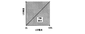
- the LED current ratio threshold value is set to 100%. In this case, PWM dimming is performed at almost all set LED current ratios.
- FIG. 16 is a graph showing an example of the relationship between the LED current and the LED luminosity.
- the solid line corresponds to DC light control
- the broken line corresponds to PWM light control.
- DC dimming the amount of decrease in LED luminous intensity tends to increase in a region where the LED current is low.
- PWM dimming the linearity of the LED luminous intensity is maintained even in a region where the LED current is low, and the decrease in the LED luminous intensity tends to be suppressed. Therefore, as described above, the amount of change in LED luminous intensity can be suppressed by performing DC dimming in a region where the LED current value is high and performing PWM dimming in a region where the LED current value is low.
- the LED current ratio threshold can be set variably as described above.
- FIG. 17 is a graph showing an example of the relationship between LED current and chromaticity.
- the solid line corresponds to DC light control
- the broken line corresponds to PWM light control.
- the change in the chromaticity is large although the change in the LED current is smaller than that in the PWM light control. Therefore, as described above, by switching between DC dimming and PWM dimming, it is possible to suppress a change in chromaticity while maintaining a high dimming rate.
- the LED driving device has a function of delay control of the LED current ON / OFF timing, which will be described below.
- FIG. 18 is a diagram showing a part of the internal configuration of the LED driving device 312 according to the second modification.
- the LED driving device 312 has a configuration in which a PD terminal is added as an external terminal and a Schmitt trigger 23 is added as an internal configuration to the LED driving device 311 (FIG. 12) according to the above-described first modification.
- the VREG terminal is connected to the PD terminal via the resistor R31.
- the signal applied to the PD terminal is input to the constant current driver 18 via the Schmitt trigger 23.
- the PD terminal is used for setting a delay time in delay control of LED current on / off timing described later.
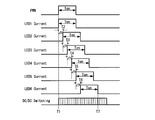
- FIG. 19 is a timing chart showing an example of the delay control of the LED current on / off timing, and shows the PWM dimming signal, the output currents ILED flowing through the LED arrays 41 to 46, and the switching pulses in order from the top.
- the constant current driver 18 turns on the constant current circuit 181 corresponding to the LED array 41 and starts flowing the output current ILED of the LED array 41.
- the generation of the switching pulse is started by the DC / DC controller 301.
- the constant current driver 18 turns on the constant current circuit 181 corresponding to the LED array 42 and starts flowing the output current ILED of the LED array 42.
- the delay time ⁇ t is set using the PD terminal.
- the constant current driver 21 turns on each of the constant current circuits 181 corresponding to the LED arrays 42 to 46 to output the respective output currents ILED of the LED arrays 42 to 46. Start flowing.
- the constant current driver 18 turns off the constant current circuit 181 corresponding to the LED array 41 to turn off the output current ILED of the LED array 41. Thereafter, at each timing delayed by the delay time ⁇ t from the timing when the output current ILED of the LED array 41 is turned off, the constant current driver 18 turns off the constant current circuits 181 corresponding to the LED arrays 42 to 46 to turn off the LED arrays 42 to 46. Each output current ILED of 46 is turned off.
- the DC / DC controller 301 switches the switching pulse.
- the PWM dimming on-duty is very low, that is, when the LED current ON period Ton is short, the output voltage Vout can be supplemented even if the output voltage Vout decreases during the period from timing T1 to T7. .
- FIG. 20 is a diagram of a package product, which is one configuration example of the LED driving device 312 according to the above-described second modification, as viewed from above.
- the LED driving device 312 shown in FIG. 20 is configured as a QFN (Quad Flat Non Lead) package.
- the IC chip is fixed to a support (a copper frame or the like) with an Ag paste or the like.
- the IC chip is connected to a lead frame (such as a copper frame) by an Au wire or the like.
- a lead frame plated eg, tin plated is formed as each external terminal. The plating surface of each external terminal is exposed on the lower surface side of the package.
- the IC chip, the support, and the lead frame are sealed with a mold resin.
- a sealing body 3121 made of a mold resin is formed in a square shape in a top view.
- the GND terminal, PD terminal, VCC terminal, CSH terminal, SD terminal, FAIL2 terminal, CPP terminal, CPM terminal, CP terminal, and FAIL1 terminal, which are external terminals, are arranged along the first side 312A of the sealing body 312. Is done.
- Unsealed terminals NC
- BOOT terminals OUTH terminals
- SW terminals SW terminals
- VDISC2 terminals VDISC1 terminals
- OVP terminals along a second side 312B extending orthogonally from one end of the first side 312A in the sealing body 312.
- OUTL terminal OUTL terminal
- CSL terminal CSL terminal
- PGND terminal is a ground terminal of the upper driver 9, the switching element 10, and the lower driver 11.
- an ISET terminal along the third side 312C facing the first side 312A in the sealing body 312, an ISET terminal, an LGND terminal, an LED1 terminal, an LED2 terminal, an LED3 terminal, an LGND terminal, an LED4 terminal, an LED5 terminal, an LED6 terminal, and an LGND
- the terminals are arranged.
- the VREG25 terminal is a terminal for outputting the voltage of 2.5 V generated by the internal voltage generation unit 1.
- the PLSET terminal and the ADIM terminal are both connected to the VREG terminal via a resistor as shown in FIGS. 1 and 12, they are arranged on the same side as the fourth side 312D where the VREG terminal is arranged. It is located near the terminal.
- the LED driving device 312 has backside heat radiation pads 3122, 3122A to 3123D.
- the back surface heat radiation pad 3122 is formed in a square shape at the center of the lower surface of the package.
- the backside heat radiating pads 3123A to 3123D are arranged at four corners of the package.
- the back surface heat radiation pad 3122 is connected to GND of the substrate on which the package is mounted.
- the backside heat dissipation pad 3122 and the backside heat dissipation pads 3123A to 3123D are short-circuited inside the package.
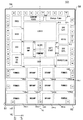
- FIG. 21 is a plan view showing the arrangement of the electrode pads and the arrangement of each area where each circuit block is arranged in the chip 101 provided in the LED driving device 312 shown in FIG.
- FIG. 21 shows an X-axis direction and a Y-axis direction orthogonal to the X-axis direction.
- the X-axis direction is more specifically shown in the X1 and X2 directions, and the Y-axis direction is more specifically.
- the X2 direction and the Y2 direction are directions approaching each other.
- the chip 101 shown in FIG. 21 has a rectangular outer shape.
- the rectangular shape has a first side S1 extending in the Y-axis direction on the X2 direction side, a second side S2 extending in the X-axis direction on the Y2 direction side, and a third side S3 extending in the Y-axis direction on the X1 direction side.
- a fourth side S4 extending in the X-axis direction on the Y1 direction side.
- the chip 101 has EN pads and other pads as electrode pads. These pads are provided in one-to-one correspondence with the terminals of the IC package shown in FIG.
- EN pad, SYNC pad, VREG25 pad, VREG pad, RT pad, PLSET pad, COMP pad, SHT pad, PWM pad, ADIM pad, ISET pad, LGND pad, LED1 pad, LED2 pad Are arranged in this order in the Y2 direction.
- the LED3 pad, the LGND pad, and the LED4 pad are arranged in this order in the X1 direction.
- the LED5 pad, the LED6 pad, the LGND pad, the PGND pad, the CSL pad, the OUTL pad, the OVP pad, the VDISC1 pad, the VDISC2 pad, the SW pad, the OUTH pad, and the BOOT pad are arranged in this order in the Y1 direction.
- a FAIL1 pad, a CP pad, a CPM pad, a CPP pad, a FAIL2 pad, an SD pad, a CSH pad, a VCC pad, a PD pad, and a GND pad are arranged in this order in the X2 direction.
- the chip 101 has regions R1 to R16 as regions where the circuit blocks are arranged.
- the region R1 is a region where the internal voltage generator 1 is arranged.
- the region R2 is a region where the spread spectrum unit 6 is arranged.
- the region R3 is a region where the oscillation unit 4 is arranged.
- the region R4 is a region where the selector 16 is arranged.
- the regions R1 to R4 are arranged in the Y2 direction near the first side S1.
- the region R5 is a region where the error amplifier 15 is arranged.
- the region R6 is a region where the slope generation unit 5 is arranged.
- the region R7 is a region where the PWM comparator 7 is arranged.
- the region R8 is a region where the soft start unit 13 is arranged.
- the region R9 is a region where the LED current setting unit 19 is arranged.
- the region R5 is arranged on the X1 direction side of the region R3, and faces the region R3 in the X direction.
- the region R5 is arranged on the X1 direction side of the region R4, and faces the region R4 in the X direction.
- the region R6 is arranged on the X1 direction side of the region R5, and faces the region R5 in the X direction.
- the region R7 is arranged on the X1 direction side of the region R5, and faces the region R5 in the X direction.
- the region R7 is arranged on the Y2 direction side of the region R6.
- the region R8 is disposed on the X1 direction side of the regions R6 and R7, and faces the regions R6 and R7 in the X direction.
- the region R9 is arranged on the Y2 direction side of the regions R5, R7, and R8.
- the region R10 is a region where the protection circuit unit 17 is arranged.
- the region R11 is a region where the lower driver 11 is arranged.
- the region R12 is a region where the output discharge unit 14 is arranged.
- the region R13 is a region where the upper driver 9 is arranged.
- the regions R10 to R13 are arranged in the Y1 direction near the third side S3.
- the region R14 is a region where the charge pump 3 is arranged.
- the region R15 is a region where the current detection unit 2 is arranged.
- the regions R14 and R15 are arranged in the X2 direction near the fourth side S4.
- the region R16 is a region where the logic unit is arranged.
- the region R16 is arranged so as to be surrounded by the regions R1, R2, R5, R6, R8, R12, R13, R14, and R15.
- YY2 direction side end region R17 (predetermined region) is arranged on the Y2 direction side of regions R4, R9 and R10.
- regions PR11, PR12, PR21, PR22, PR31, and PR32 in which the MOSFETs included in the constant current driver 18 are arranged, and regions in which the driver amplifiers included in the constant current driver 18 are arranged DR11, DR12, DR21, DR22, DR31, DR32 are arranged.
- the regions PR31 and DR31 correspond to the LED array 41
- the regions PR21 and DR21 correspond to the LED array 42
- the regions PR11 and DR11 correspond to the LED array 43
- the regions PR12 and DR12 correspond to the LED array 44
- the regions PR22 and DR22 correspond to the LED array 45
- the regions PR32 and DR32 correspond to the LED array 46.
- the regions DR11 and DR12 are formed symmetrically with respect to a center line CL of the chip 101 extending in the Y-axis direction.
- the regions PR11 and PR12 are formed symmetrically with respect to the center line CL outside the regions DR11 and DR12 in the X-axis direction, respectively.
- a set including the regions PR21 and PR22 and the regions DR21 and DR22 is arranged on the Y1 direction side of a set including the regions PR11 and PR12 and the regions DR11 and DR12.
- the regions DR21 and DR22 are formed symmetrically with respect to the center line CL.
- the regions PR21 and PR22 are formed symmetrically with respect to the center line CL outside the regions DR21 and DR22 in the X-axis direction, respectively.
- a set including the regions PR31 and PR32 and the regions DR31 and DR32 is arranged on the Y1 direction side of a set including the regions PR21 and PR22 and the regions DR21 and DR22.
- the regions DR31 and DR32 are formed symmetrically with respect to the center line CL.
- the regions PR31 and PR32 are formed symmetrically with respect to the center line CL outside the regions DR31 and DR32 in the X-axis direction, respectively.
- An LGND pad LG1 and an LED1 pad are arranged in the region PR31.
- the LED2 pad is arranged in the area PR21.
- the LED3 pad is arranged in the area PR11.
- An LED4 pad is arranged in the area PR12.
- An LED5 pad is arranged in the area PR22.
- an LGND pad LG2 and an LED6 pad are arranged.
- the LGND pad LG3 is arranged so as to be sandwiched in the X direction by the regions DR11 and DR12.
- the LED pads LG1 and LG2 are connected by a first line (not shown) extending in the X direction.
- the first line is connected to the LGND pad LG3 by a second line (not shown) extending in the Y direction.
- the first line and the second line are thick wiring to reduce impedance.
- the impedance of each LED system can be reduced while reducing the number of pads.
- the region TD in which the TSD portion is arranged is arranged at the center of the Y2 direction side end region R17. Thereby, the temperature can be detected at a position where a temperature gradient does not occur with respect to the Y2 direction side end region R17 that becomes the heat generating portion.
- the area TD should be arranged between the Y2 direction side end area R17 and the area R16 where the logic section is arranged. Is desirable.
- FIG. 22 shows a configuration example of a backlight device to which the LED driving device according to the embodiment of the present invention can be applied.
- the configuration shown in FIG. 22 is of a so-called edge light type, and is not limited thereto, and may be of a direct type.
- the backlight device 70 shown in FIG. 22 is an illumination device that illuminates the liquid crystal panel 81 from the back.
- the backlight device 70 includes an LED light source unit 71, a light guide plate 72, a reflection plate 73, and optical sheets 74.
- the LED light source 71 includes an LED and a substrate on which the LED is mounted.
- the light emitted from the LED light source unit 71 enters inside from the side surface of the light guide plate 72.
- the light guide plate 72 formed of an acrylic plate guides the light that has entered therein to the entire interior while totally reflecting the light, and emits the light as planar light from the surface on which the optical sheets 74 are disposed.
- the reflection plate 73 reflects light leaked from the light guide plate 72 and returns the light to the inside of the light guide plate 72.
- the optical sheets 74 are made of a diffusion sheet, a lens sheet, or the like, and aim at uniforming the luminance of light illuminating the liquid crystal panel 81, improving the luminance, and the like.
- the LED light source unit 71 includes the LED driving device according to the embodiment of the present invention, an output stage, and an LED.
- the backlight device to which the above-described LED drive device according to the embodiment of the present invention is applied is particularly preferably mounted on a vehicle-mounted display.
- the dimming range of the LED can be expanded, so that the display brightness can be increased in daytime driving and nighttime driving, or in daytime normal driving and driving in a tunnel. It is suitable for in-vehicle displays that need to be adjusted.
- the in-vehicle display is provided on the dashboard in front of the driver's seat of the vehicle, for example, like the in-vehicle display 85 shown in FIG.
- the in-vehicle display 85 can display various images such as car navigation information, a captured image of the rear of the vehicle, a speedometer, a fuel gauge, a fuel consumption meter, a shift position, and the like, and can convey various information to the user.
- Such an in-vehicle display is also called a cluster panel or a center information display (CID).
- the in-vehicle display may be, for example, rear entertainment arranged behind a driver's seat or a passenger seat.
- the present invention can be used, for example, as a driving unit of a vehicle-mounted LED.
Landscapes
- Engineering & Computer Science (AREA)
- Mechanical Engineering (AREA)
- Circuit Arrangement For Electric Light Sources In General (AREA)
- Dc-Dc Converters (AREA)
- Led Devices (AREA)
Abstract
入力電圧から出力電圧を生成してLEDに供給するための出力段を制御するDC/DCコントローラと、前記LEDの出力電流を生成する電流ドライバと、を有し、前記電流ドライバは、前記PWM調光信号のLED電流オン期間に応じて前記出力電流をオンとし、前記PWM調光信号のLED電流オフ期間に応じて前記出力電流をオフとすることでPWM調光を行い、前記DC/DCコントローラは、前記LEDのカソード電圧を基準電圧に一致させるべく前記出力段にスイッチングパルスを出力する帰還制御を行う帰還制御部と、前記LED電流オン期間と前記LED電流オフ期間との間での切替わりのときに所定パルス数の追加スイッチングパルスを追加するパルス付加制御を行うパルス付加制御部と、を有し、前記所定パルス数は、可変設定される、LED駆動装置。
Description
本発明は、LED駆動装置に関する。
従来、消費電力が小さく寿命の長いLED(発光ダイオード)が様々な用途に用いられる。LEDを駆動するLED駆動装置の従来例は、特許文献1に開示されている。
特許文献1のLED駆動装置は、入力電圧から出力電圧を生成してLEDに供給するための出力段を制御するDC/DCコントローラと、LEDに流れる出力電流を生成する定電流ドライバと、を有し、複数系統のLEDを駆動する。
DC/DCコントローラは、複数系統のLEDのカソード電圧のうち最低電圧と基準電圧とを比較するエラーアンプと、当該エラーアンプの出力とスロープ信号とを比較して内部PWM信号を生成するPWMコンパレータと、を有する。
定電流ドライバは、PWM端子に入力される外部PWM信号に基づいてオンオフされる。これにより、PWM調光制御が行われる。定電流ドライバがオンの期間において、エラーアンプおよびPWMコンパレータにより上記カソード電圧の最低電圧が基準電圧と一致するように出力段におけるスイッチング素子がスイッチングパルスによりPWM駆動される。これにより、複数系統のLEDの各順方向電圧のうちの最大電圧に上記基準電圧を加えた電圧値に出力電圧(LEDのアノード電圧)が制御される。
しかしながら、PWM調光制御のオンデューティが非常に低い場合に、定電流ドライバがオンとなる期間が短くなり、スイッチングパルスのパルス数が不足し、定電流ドライバのオン期間ごとに出力電圧が低下する現象が生じる。これにより、LEDに流れる電流が不安定となり、LEDを正常に点灯できない虞があった。すなわち、PWM調光制御のオンデューティの対応範囲が狭くなり、調光率を高くできないという問題があった。
特に昨今、例えば車載用の表示装置では、環境光の明るさの変化が大きく、LEDの調光率を高くすることが要望されている。
上記状況に鑑み、本発明は、PWM調光の調光率を高めることが可能となるLED駆動装置を提供することを目的とする。
本発明の一態様に係るLED駆動装置は、
入力電圧から出力電圧を生成してLEDに供給するための出力段を制御するDC/DCコントローラと、
前記LEDの出力電流を生成する電流ドライバと、
を有し、
前記電流ドライバは、PWM調光信号のLED電流オン期間に応じて前記出力電流をオンとし、前記PWM調光信号のLED電流オフ期間に応じて前記出力電流をオフとすることでPWM調光を行い、
前記DC/DCコントローラは、
前記LEDのカソード電圧を基準電圧に一致させるべく前記出力段にスイッチングパルスを出力する帰還制御を行う帰還制御部と、
前記LED電流オン期間と前記LED電流オフ期間との間での切替わりのときに所定パルス数の追加スイッチングパルスを追加するパルス付加制御を行うパルス付加制御部と、
を有し、
前記所定パルス数は、可変設定される構成としている。
入力電圧から出力電圧を生成してLEDに供給するための出力段を制御するDC/DCコントローラと、
前記LEDの出力電流を生成する電流ドライバと、
を有し、
前記電流ドライバは、PWM調光信号のLED電流オン期間に応じて前記出力電流をオンとし、前記PWM調光信号のLED電流オフ期間に応じて前記出力電流をオフとすることでPWM調光を行い、
前記DC/DCコントローラは、
前記LEDのカソード電圧を基準電圧に一致させるべく前記出力段にスイッチングパルスを出力する帰還制御を行う帰還制御部と、
前記LED電流オン期間と前記LED電流オフ期間との間での切替わりのときに所定パルス数の追加スイッチングパルスを追加するパルス付加制御を行うパルス付加制御部と、
を有し、
前記所定パルス数は、可変設定される構成としている。
本発明のLED駆動装置によれば、PWM調光の調光率を高めることが可能となる。
以下に本発明の一実施形態について図面を参照して説明する。なお、以下に記載する具体的な信号値や温度値等は、一例である。
<1.LED駆動装置の構成>
図1は、本発明の一実施形態に係るLED駆動装置30の構成を示した回路構成図である。図1に示すLED駆動装置30は、複数系統(本実施例では6系統)のLEDアレイ41~46を駆動する。LED駆動装置30は、内部電圧生成部1と、電流検出部2と、チャージポンプ3と、発振部4と、スロープ生成部5と、スペクトラム拡散部6と、PWMコンパレータ7と、制御ロジック部8と、上側ドライバ9と、トランジスタ10と、下側ドライバ11と、シュミットトリガ12と、ソフトスタート部13と、出力ディスチャージ部14と、エラーアンプ15と、セレクタ16と、保護回路部17と、定電流ドライバ18と、LED電流設定部19と、基準電圧源20と、シュミットトリガ21と、を集積化して有する半導体装置である。
図1は、本発明の一実施形態に係るLED駆動装置30の構成を示した回路構成図である。図1に示すLED駆動装置30は、複数系統(本実施例では6系統)のLEDアレイ41~46を駆動する。LED駆動装置30は、内部電圧生成部1と、電流検出部2と、チャージポンプ3と、発振部4と、スロープ生成部5と、スペクトラム拡散部6と、PWMコンパレータ7と、制御ロジック部8と、上側ドライバ9と、トランジスタ10と、下側ドライバ11と、シュミットトリガ12と、ソフトスタート部13と、出力ディスチャージ部14と、エラーアンプ15と、セレクタ16と、保護回路部17と、定電流ドライバ18と、LED電流設定部19と、基準電圧源20と、シュミットトリガ21と、を集積化して有する半導体装置である。
また、LED駆動装置30は、外部との電気的接続を確立するための外部端子として、VCC端子、VREG端子、CSH端子、SD端子、CPP端子、CPM端子、CP端子、BOOT端子、OUTH端子、SW端子、OUTL端子、CSL端子、VDISC端子、LED1端子~LED6端子、PGND端子、OVP端子、LGND端子、GND端子、ISET端子、PWM端子、SHT端子、FAIL1端子、FAIL2端子、COMP端子、PLSET端子、SYNC端子、RT端子、および、EN端子を有する。
LED駆動装置30の外部には、入力電圧Vinから出力電圧VoutをDC/DC変換により生成してLEDアレイ41~46に供給するための出力段35が配置される。出力段35は、コンデンサCvccと、抵抗Rshと、スイッチング素子N1と、ダイオードD1と、インダクタL1と、ダイオードD2と、スイッチング素子N2と、出力コンデンサCoと、コンデンサCbtと、を有する。スイッチング素子N1、N2がLED駆動装置30により駆動制御されることにより、出力段35はLED駆動装置30により制御される。出力段35とLED駆動装置30とにより、DC/DCコンバータが形成される。なお、本実施形態では、特にDC/DCコンバータとして、昇降圧DC/DCコンバータが構成される。
入力電圧Vinの印加端は、コンデンサCvccの一端に接続される。コンデンサCvccの他端は、接地端に接続される。入力電圧Vinの印加端は抵抗Rshの一端に接続される。抵抗Rshの他端は、pチャネルMOSFETで構成されるトランジスタM1のソースに接続される。トランジスタM1のドレインは、nチャネルMOSFETで構成されるスイッチング素子N1のドレインに接続される。スイッチング素子N1のソースは、ダイオードD1のカソードに接続される。ダイオードD1のアノードは、接地端に接続される。スイッチング素子N1のゲートは、OUTH端子に接続される。
スイッチング素子N1とダイオードD1とが接続されるノードには、インダクタL1の一端が接続される。インダクタL1の他端は、ダイオードD2のアノードとともにnチャネルMOSFETで構成されるスイッチング素子N2のドレインに接続される。スイッチング素子N2のソースは、抵抗Rslを介して接地端に接続される。スイッチング素子N2のゲートは、OUTL端子に接続される。ダイオードD2のカソードは、出力コンデンサCoの一端に接続される。出力コンデンサCoの他端は、接地端に接続される。出力コンデンサCoの一端に出力電圧Voutが生成される。
スイッチング素子N1とダイオードD1とが接続されるノードには、SW端子とともにブートストラップ用のコンデンサCbtの一端が接続される。コンデンサCbtの他端は、BOOT端子に接続される。
なお、スイッチング素子N1とスイッチング素子N2のうち少なくとも一方をLED駆動装置に含めるようにしてもよい。
出力電圧Voutが発生する出力コンデンサCoの一端には、LEDアレイ41~46の各アノードが接続される。LEDアレイ41~46は、それぞれ直列に接続された複数のLEDから構成される。LEDアレイ41~46の各カソードは、それぞれLED1端子~LED6端子に接続される。
なお、LEDアレイ41~46は、それぞれ直列接続に限らず、例えば直並列に接続されたLEDから構成されてもよいし、1つのみのLEDから構成されてもよい。また、駆動可能なLEDアレイの個数も6つに限らず、例えば4つ等でもよい。また、1系統のLEDアレイのみを駆動可能としてもよい。
次に、LED駆動装置30の内部構成に関して説明する。
内部電圧生成部1は、EN端子がHighのときに、VCC端子に印加される入力電圧Vinから内部電圧Vreg(例えば5V)を生成してVREG端子から出力する。内部電圧Vregは、LED駆動装置30に含まれる内部回路の電源電圧として使用される。VREG端子には、コンデンサCvgが接続される。
電流検出部2には、CSH端子、CSL端子、および、SD端子が接続される。
チャージポンプ3には、CPP端子、CPM端子、および、CP端子が接続される。CPP端子とCPM端子との間には、チャージポンプ用のコンデンサCcp1が接続される。チャージポンプ3の出力用端子であるCP端子には、コンデンサCcp2が接続される。チャージポンプ3は、入力された内部電圧Vregを昇圧してCP端子から出力する。
発振部4は、SYNC端子への入力信号、または、RT端子の端子電圧に応じて、所定のクロック信号を生成し、これをスロープ生成部5に出力する。
スロープ生成部5は、発振部4から入力されるクロック信号に基づいて、スロープ信号(三角波信号)Vslpを生成し、これをPWMコンパレータ7に出力する。また、電流検出部2は、スイッチング素子N2に流れる電流を抵抗Rslにより変換したCSL端子電圧に応じて、スロープ信号Vslpにオフセットを与える機能を有する。
RT端子に接続される抵抗Rrtの抵抗値を調整することにより、発振部4の内部キャパシタに対する充放電電流が決定され、スロープ信号の発振周波数(延いては昇降圧DC/DCコンバータの発振周波数FOSC)を設定することができる。LED駆動装置30は、昇降圧DC/Dコンバータを外部同期させるためのクロック入力を受け付けるSYNC端子を備えている。LED駆動装置30では、RT端子またはSYNC端子を用いて、DC/DCコンバータの発振周波数を任意にかつ高精度に可変制御することが可能である。例えば、車載用表示装置のバックライト制御手段として、LED駆動装置30を用いる場合、ラジオ受信周波数の切替制御に合わせてSYNC端子から外部同期発振周波数を適宜設定してやれば、DC/DCコンバータの発振周波数がラジオノイズの周波数帯に重なることを回避することができるので、ラジオの受信品質を損わずに、バックライト制御を行うことが可能となる。
スペクトラム拡散部6は、DC/DCコンバータのスイッチング周波数を変化させることで、ノイズの平均を下げることができる。SYNC端子によりスペクトラム拡散部6のオン/オフが切替えられる。
PWMコンパレータ7は、非反転入力端(+)に入力される誤差信号Verrと、反転入力端(-)に入力されるスロープ信号Vslpとを比較して内部PWM信号を生成し、これを制御ロジック部8に出力する。
制御ロジック部8は、内部PWM信号に基づいて上側ドライバ9、トランジスタ10、および下側ドライバ11の駆動信号を生成する。
上側ドライバ9は、制御ロジック部8から入力される駆動信号に基づいて、OUTH端子電圧(スイッチング素子N1のゲート電圧)をBOOT端子電圧とSW端子電圧との間でパルス駆動する。スイッチング素子N1は、上側ドライバ9から入力されるゲート電圧に基づいてオン/オフされる。
スイッチング素子10は、制御ロジック部8から入力される駆動信号に基づいてオン/オフされ、SW端子と接地端との間を導通/遮断する。
下側ドライバ11は、制御ロジック部8から入力される駆動信号に基づいてスイッチング素子N2のゲート電圧をチャージポンプ3の出力電圧CPと接地電圧との間でパルス駆動する。
スイッチング素子N2は、下側ドライバ11から入力されるゲート電圧に基づいてオン/オフされる。
LED1端子~LED6端子には、それぞれLEDアレイ41~46の各カソード電圧としてLED端子電圧Vled1~Vled6が印加される。セレクタ16は、LED端子電圧Vled1~Vled6のうち最低電圧を選択してエラーアンプ15の一方の反転入力端(-)に出力する。エラーアンプ15の他方の反転入力端(-)には、出力電圧Voutを分圧抵抗Rovp1,Ropv2によって分圧した後のOVP端子電圧が印加される。エラーアンプ15の非反転入力端(+)には、基準電圧Vrefが印加される。エラーアンプ15は、2つの反転入力端(-)に印加される電圧のうち低い方の電圧と、基準電圧Vrefとの差分を増幅して誤差信号Verrを生成し、これをPWMコンパレータ7に出力する。起動時のみ起動を早めるためにOVP端子に基づく帰還制御が行われ、起動後はセレクタ16の出力に基づく帰還制御が行われる。
エラーアンプ15の出力端は、COMP端子に接続される。COMP端子には、外部において直列接続される抵抗RpcとコンデンサCpcを介して接地端に接続される。
ソフトスタート部13は、誤差信号Verrの電圧レベルを緩やかに高めていくように制御する。これにより、出力電圧Voutのオーバーシュートや突入電流を抑制できる。
保護回路部17は、TSD部(過熱保護回路)と、OCP部と、OVP部と、LEDオープン検出回路(OPEN)と、LEDショート検出回路(SHORT)と、出力短絡保護回路(SCP)と、UVLO部と、を含む。
TSD部は、LED駆動装置30のジャンクション温度が例えば175℃以上となったときに、内部電圧生成部1以外の回路をシャットダウンする。なお、TSD部は、LED駆動装置30のジャンクション温度が例えば150℃となったときに、回路動作を復帰させる。
電流検出部2は、スイッチング素子N1に流れる電流を抵抗Rshにより電圧信号として検出したCSH端子電圧(入力電流検出電圧)を監視し、CSH端子電圧が例えばVin-0.6V以下となったときに過電流保護をかけるようOCP部に指令する。OCP部は、過電流保護をかける際、DC/DCスイッチングをオフさせる。
また、SD端子には、トランジスタM1のゲートが接続される。電流検出部2は、抵抗Rshに流れる過電流(インダクタL1に流れる過電流)を検出したときに、トランジスタM1をオフとし、入力電圧Vinの印加端からインダクタL1への経路を遮断する。
OVP部は、OVP端子電圧を監視し、OVP端子電圧が例えば2.0V以上となったときに過電圧保護をかける。過電圧保護をかけたとき、DC/DCスイッチングがオフされる。
LEDオープン検出回路(OPEN)では、LED端子電圧Vled1~Vled6のいずれかが例えば0.3V以下で、かつ、OVP端子電圧が例えば2.0V以上のときに、LEDオープン検出がかかり、オープン検出されたLEDアレイのみラッチオフされる。
LEDショート検出回路(SHORT)では、LED端子電圧Vled1~Vled6のいずれかが例えば4.5V以上のときに、内蔵されているカウンタ動作が開始され、約100ms(FOSC=300kHz時)経過後にラッチがかかり、ショート検出されたLEDアレイのみラッチオフされる。SHT端子には、LEDショート保護設定用の抵抗Rshtが接続される。
出力短絡保護回路(SCP)では、OVP端子電圧が例えば0.57V以下となったとき、または、LED端子電圧Vled1~Vled6のいずれかが例えば0.3V以下になったときに、内蔵されているカウンタ動作が開始され、約100ms(FOSC:300kHz時)経過後にラッチがかかり内部電圧生成部1以外の回路をシャットダウンする。出力短絡保護回路は、LEDアレイ41~46のアノード側(DC/DC出力端側)が地絡したとき、LEDアレイ41~46のカソード側が地絡したときのいずれの場合の地絡保護にも対応している。
UVLO部は、入力電圧Vinが例えば3.5V以下になったとき、または、内部電圧Vregが例えば2.0V以下になったときに、内部電圧生成部1以外の回路をシャットダウンする。
保護回路部17は、OVP部およびOCP部の異常検出状態に基づき、FAIL1端子から外部へ異常検出信号を出力する。FAIL1端子には、抵抗Rf1を介してVREG端子が接続される。OVP部、OCP部のいずれかが異常を検出したときに、保護回路部17は、FAIL1端子に接続される不図示のトランジスタをオンとすることにより、FAIL1端子をLow出力とする。
また、保護回路部17は、LEDオープン検出回路、LEDショート検出回路、および出力短絡保護回路(SCP)の異常検出状態に基づき、FAIL2端子から外部へ異常検出信号を出力する。FAIL2端子には、抵抗Rf2を介してVREG端子が接続される。LEDオープン検出回路、LEDショート検出回路、および出力短絡保護回路(SCP)のいずれかが異常を検出したときに、保護回路部17は、FAIL2端子に接続される不図示のトランジスタをオンとすることにより、FAIL2端子をLow出力とする。
シュミットトリガ21は、PWM端子へ外部から入力されるPWM調光信号を定電流ドライバ18に伝達する。PWM調光信号は、パルス信号として入力される。
また、LED電流設定部19は、ISET端子に接続される抵抗Risetの抵抗値に応じた定電流値を定電流ドライバ18に設定する。また、基準電圧源20は、基準電圧Vrefを生成する。
定電流ドライバ18は、LED1端子~LED6端子の各端子と、接地端に接続されるLGND端子との間に配置される6系統分の定電流回路181を有する。定電流ドライバ18は、PWM制御ロジック部182を更に有する。PWM制御ロジック部182は、PWM調光信号の示すPWM調光のオンデューティに応じて、定電流回路181をオンオフ制御する。具体的には、PWM調光のオンデューティに応じたLED電流オン期間で定電流回路181をオンとし、PWM調光のオンデューティに応じたLED電流オフ期間で定電流回路181をオフとする。定電流回路181がオンのとき、LED電流設定部19により設定された定電流値の出力電流ILEDが流れる。
また、VDISC端子は、出力ディスチャージ部14に接続される。VDISC端子は、出力電圧Voutの生成される出力コンデンサCoの一端に接続される。出力コンデンサCoに電荷が残っている状態で起動した場合、LEDのちらつきが発生する可能性がある。そのため、起動時には出力コンデンサCoの放電が必要となるが、OVP設定用の抵抗Rovp1,Rovp2などの放電経路だけでは電荷の放電に時間がかかる場合があるため、出力ディスチャージ部14により出力コンデンサCoの残留電荷の放電を行う。当該放電は、DC/DCコンバータのオフ時(EN端子に印加する信号の立ち下げ時や保護時)に行われる。
また、GND端子は、LED駆動装置30内部の小信号ブロックのGNDを印加するための端子である。
<2.DC/DCコントローラ>
次に、LED駆動装置30の有するDC/DCコントローラ301(発振部4、スロープ生成部5、PWMコンパレータ7、制御ロジック部8、上側ドライバ9、トランジスタ10、下側ドライバ11、およびエラーアンプ15を含む回路ブロック)について詳述する。
次に、LED駆動装置30の有するDC/DCコントローラ301(発振部4、スロープ生成部5、PWMコンパレータ7、制御ロジック部8、上側ドライバ9、トランジスタ10、下側ドライバ11、およびエラーアンプ15を含む回路ブロック)について詳述する。
エラーアンプ15は、セレクタ16により選択されたLED端子電圧Vled1~Vled6の最低値と、OVP端子電圧とのうち低い方の電圧と、基準電圧Vrefとの差分を増幅して誤差電圧Verrを生成する。誤差電圧Verrの電圧値は、上記低い方の電圧が基準電圧Vrefよりも低いほど高レベルとなる。
PWMコンパレータ7は、誤差電圧Verrとスロープ信号Vslpとを比較して内部PWM信号を生成する。内部PWM信号は、誤差電圧Verrがスロープ信号Vslpよりも高ければハイレベルとなり、誤差電圧Verrがスロープ信号Vslpよりも低ければローレベルとなる。
制御ロジック部8は、内部PWM信号に基づいてスイッチング素子N1、トランジスタ10およびスイッチング素子N2のオン/オフ制御を行う。具体的に述べると、制御ロジック部8は、内部PWM信号がハイレベルであるときに、スイッチング素子N1、N2をオンとし、トランジスタ10をオフとする。逆に、制御ロジック部8は、内部PWM信号がローレベルであるときに、スイッチング素子N1、N2をオフとし、トランジスタ10をオンとする。
これにより、エラーアンプ15、PWMコンパレータ7、制御ロジック部8、上側ドライバ9、および下側ドライバ11からなる帰還制御部は、LED端子電圧Vled1~Vled6の最低値を基準電圧Vrefと一致させるべくスイッチングパルスをOUTH、OUTL端子からスイッチング素子N1、N2へ出力する帰還制御を行う。すなわち、DC/DCコントローラ301は、上記帰還制御部を有する。
スイッチング素子N1、N2がオンされてトランジスタ10がオフされると、入力電圧Vinの印加端から抵抗Rsh、スイッチング素子N1、インダクタL1、および、スイッチング素子N2を介して接地端に至る経路で電流が流れ、インダクタL1に電気エネルギが蓄えられる。このとき、出力コンデンサCoに電荷が蓄積されていた場合には、LEDアレイ41~46のアノードに対して、出力コンデンサCoから出力電流ILEDが流れることになる。なお、ダイオードD2は逆バイアス状態となっているので、出力コンデンサCoからスイッチング素子N2に向けて電流が流れ込むことはない。
スイッチング素子N1、N2がオフされてトランジスタ10がオンされると、インダクタL1に生じた逆起電力により、接地端からトランジスタ10、インダクタL1、および、ダイオードD2を介する経路で電流が流れる。この電流は、出力電流ILEDとしてLEDアレイ41~46に流れ込むとともに、出力コンデンサCoを介して接地端にも流れ込み、出力コンデンサCoを充電することになる。
上記の動作が繰り返されることにより、LEDアレイ41~46には、入力電圧Vinを昇降圧して得られた出力電圧Voutが供給される。
なお、スイッチング素子N1のデューティ比(一周期に占めるオン期間の割合)が50%よりも小さければ、入力電圧Vinの降圧動作が行われることになり、スイッチング素子N1のデューティ比が50%よりも大きければ、入力電圧Vinの昇圧動作が行われることになる。このように、LED駆動装置30であれば、簡易な構成でありながら、容易かつ適切に、その昇降圧動作を切り換えることが可能となる。
従って、LED駆動装置30であれば、入力電圧Vinが所望の出力電圧Voutよりも高いか低いかに依ることなく、常に所望の出力電圧Voutを得ることが可能となる。例えば、出力電圧Voutの所望値が16Vであるのに対して、入力電圧Vinが6~18Vの範囲で変動する場合であっても、所望の出力電圧Voutを得ることが可能となる。このような構成は、例えば、バッテリから直接供給される入力電圧Vinに対応する必要のあるアプリケーション(例えばカーナビモニタのバックライト制御用LEDドライバIC)に好適である。
また、LED駆動装置30は、軽負荷時或いは無負荷時におけるリンギング防止手段としてトランジスタ10を有する。トランジスタ10の電流能力は、不要なチップ面積の増大や変換効率の低下を招かぬように、リンギングノイズという微小電流を引き抜き得る必要最小限に設計することが望ましい。トランジスタ10は、スイッチング素子N1、N2とは、相補的(排他的)にスイッチング制御される。
このような構成とすることにより、軽負荷時や無負荷時に、出力電流ILEDが低下してリンギングと呼ばれる波形の乱れが生じる状態(いわゆる不連続モード)に陥った場合であっても、トランジスタ10を介してリンギングノイズを接地端に逃がすことができるので、昇降圧動作の安定性を高めることが可能となる。
なお、上記の説明中で用いた「相補的(排他的)」という文言は、スイッチング素子N1、N2とトランジスタ10のオン/オフが完全に逆転している場合のほか、貫通電流防止等の観点から、スイッチング素子N1、N2とトランジスタ10の同時オフ期間が設けられている場合をも含むものとする。
<3.スイッチングパルス付加制御>
次に、本実施形態に係るLED駆動装置30に備えられる機能であるスイッチングパルス付加制御に関して説明する。
次に、本実施形態に係るLED駆動装置30に備えられる機能であるスイッチングパルス付加制御に関して説明する。
図2は、パルス付加制御に対する比較例としてのタイミングチャートであり、上段からPWM調光信号、OUTH,OUTL端子から出力されるスイッチングパルス、出力電圧Vout、および出力電流ILEDを示す。なお、PWM調光信号は、High(オンレベル)がLED電流オン、Low(オフレベル)がLED電流オフを示す。
図2に示すように、タイミングt1においてPWM制御ロジック部182により定電流回路181は出力電流ILEDをオンとする。これにより、LED端子電圧Vled1~Vled6がLEDアレイ41~46の順方向電圧によって急峻に低下し、エラーアンプ15およびPWMコンパレータ7の動作によってDC/DCコントローラ301は、OUTH,OUT端子からスイッチングパルスの出力を開始する。タイミングt2においてPWM制御ロジック部182により、定電流回路181は出力電流ILEDをオフとする。これにより、LED端子電圧Vled1~Vled6が急峻に上昇するので、DC/DCコントローラ301によるOUTH,OUTL端子からのスイッチングパルスはオフレベルで停止される。
スイッチングパルスの出力開始時にはLEDアレイ41~46によるLED負荷によって出力電圧Voutが低下する。これは、スイッチングパルスの出力開始時にはインダクタL1に流れる電流はゼロから上昇してインダクタL1にエネルギーが徐々に蓄えられるが、それと同時にLED負荷が発生するからである。図2に示すようにPWM調光のオンデューティが非常に低く、タイミングt1~t2間の期間が短い場合、スイッチングパルスが足りず、出力電圧Voutが低下途中のタイミングt2で出力電流ILEDがオフとされ、出力電圧Voutは保持される。
その後、同様にタイミングt3でLED電流がオンとなると、スイッチングパルスの出力が開始されるが、LED負荷によって出力電圧Voutがさらに低下し、出力電流ILEDが不安定となり、LEDを正常に点灯できない虞がある。すなわち、PWM調光のオンデューティが非常に低い場合、スイッチングパルスが足りなくなり、出力電圧VoutがLED電流のオンごとに低下してしまい、出力電圧Voutが不足になる現象が生じる可能性がある。
そこで、本実施形態では、図3に示すタイミングチャートのように、PWM調光のLED電流オン期間からLED電流オフ期間へ切替わるタイミングt2後に、制御ロジック部8(すなわちDC/DCコントローラ301)は、OUTH,OUTL端子から所定数のスイッチングパルスを追加して出力する。すなわち、制御ロジック部8は、パルス付加制御を行うパルス付加制御部に相当する。これにより、図3に示すように、LED電流オフへの切替え後に出力コンデンサCoが充電され、出力電圧Voutが上昇する。これにより、タイミングt3~t4のLED電流オン期間で出力電圧Voutが低下しても、出力電流ILEDは不安定とならない。
すなわち、PWM調光のオンデューティが非常に低い場合でも、LED電流オン期間で低下した出力電圧Voutを、追加したスイッチングパルスによって補うので、出力電圧Voutを保持でき、出力電流ILEDを安定化して、LEDの点灯を正常に行うことができる。
なお、DC/DCコントローラ301は、追加するスイッチングパルスのデューティとして、直前のLED電流オン期間(t1~t2)における最後のスイッチングパルスのデューティを保持して用いる。また、DC/DCコントローラ301は、LED電流オン期間(t3~t4)が始まるときのスイッチングパルスとしては、前回のLED電流オン期間(t1~t2)における最後のスイッチングパルスのデューティを用いる。
図2に示すようなスイッチングパルスの追加を行わない制御を用いた場合のPWM調光オンデューティと出力電流ILEDとの関係の一例を図4のグラフに示す。図4の例では、PWM調光オンデューティが0.1%付近より低くなると、出力電流ILEDの低下量が大きくなってしまう。
これに対し、本実施形態の図3に示したようなスイッチングパルスを追加するパルス付加制御を行った場合のPWM調光オンデューティと出力電流ILEDとの関係の一例を図5のグラフに示す。図4に対して図5では、PWM調光オンデューティが0.1%付近より低い場合でも、出力電流ILEDの低下量を抑えることができる。すなわち、図5に示す例であれば、100%~0.01%までのPWM調光オンデューティに対応することが可能であり、調光率は10000倍となって、高調光率を実現できる。
なお、上述したパルス付加制御は、PWM調光オンデューティを下限(例えば0.01%)から上限(例えば100%)までの全ての範囲で行うことが望ましい。これにより、PWM調光オンデューティの切替え時に、制御モードが切替わってLED電流の低下によって輝度が不安定となることを回避できる。ただし、PWM調光オンデューティが高い場合は、LED電流オン期間で出力電圧Voutが十分に保持できる場合もあるので、その場合は、例えば、PWM調光オンデューティが所定の閾値より低い場合のみにパルス付加制御を行ってもよい。
<4.追加パルス数の可変制御>
ここで、図6は、上述したパルス付加制御の一例を示すタイミングチャートであり、上段から出力電圧Vout、OUTH,OUTL端子から出力されるスイッチングパルス、、PWM調光信号、およびLEDを流れる出力電流ILEDを示す。図6は、先述した図3よりも、より具体的な波形を示している。
ここで、図6は、上述したパルス付加制御の一例を示すタイミングチャートであり、上段から出力電圧Vout、OUTH,OUTL端子から出力されるスイッチングパルス、、PWM調光信号、およびLEDを流れる出力電流ILEDを示す。図6は、先述した図3よりも、より具体的な波形を示している。
図6は、PWM調光オンデューティが低い場合、すなわちタイミングt11~t12の期間であるLED電流オン期間が短い場合であり、当該期間でスイッチングパルスが出力されるが、スイッチングパルスが足りずLED負荷によって出力電圧Voutは低下する。そして、LED電流がオフとなるタイミングt12後に、パルス数が12個のスイッチングパルスが追加されている。これにより、出力電圧Voutは補われる。
ここで、図7は、図6に対応する図であるが、図6に比べてLED負荷が軽負荷である場合を示す。この場合、タイミングt11~t12の期間であるLED電流オン期間での出力電圧Voutの低下量は抑えられる。このような場合に、仮に、図6と同様に12個のスイッチングパルスを追加してしまうと、出力電圧Voutが過剰に補われる。これにより、出力電圧Voutに生じるリップルが大きくなる虞がある。リップルが大きくなると、出力コンデンサCoに生じる音鳴りが大きくなる虞がある。
LED駆動装置30として、出力電圧Voutの補充を優先させるため、LED駆動装置30によって駆動可能なLED負荷のうち最大の負荷の場合に応じて、固定の追加パルス数を設定することも可能である。しかしながら、この場合、上述のようにLED負荷が軽負荷の場合に、出力電圧Voutの補充が過剰となって出力電圧Voutのリップルが大きくなる虞がある。または、リップルを抑えるために、出力コンデンサCoの容量を調整する必要がある。
このようなことに鑑み、本実施形態では、追加パルス数は可変設定される。具体的には、図7においては、図6に比べてLED負荷が軽負荷であり、LED電流オン期間での出力電圧Voutの低下量が抑えられるので、図6よりも少ない4個のパルス数のスイッチングパルスを追加している。これにより、追加パルスによる出力電圧Voutの補充が適切となる。従って、出力電圧Voutに生じるリップルを抑えることができ、出力コンデンサCoの音鳴りを抑制できる。
このように、LED駆動装置30によって駆動させるLED負荷(LED個数、LED電流値仕様)に応じて、制御ロジック部8は、追加するスイッチングパルスのパルス数を可変とする。例えば、LED駆動装置30が車載用表示装置のバックライト用であれば、車載用表示装置の表示サイズに応じてLED負荷が変化する。
制御ロジック部8は、PLSET端子を用いて追加パルス数を可変とする。より具体的には、図8に示すように、VREG端子と接地端との間に抵抗R11、R12を直列に接続し、抵抗R11とR12との接続ノードにPLSET端子を接続する。PLSET端子に印加される電圧は、シュミットトリガ12を介して制御ロジック部8に入力される。抵抗R11,R12の抵抗値の組み合わせによってVREG端子に生成される内部電圧Vregの分圧比が変化し、PLSET端子に印加される電圧が変化する。従って、制御ロジック部12は、PLSET端子に印加される電圧に応じてOUTH,OUTL端子から出力させる追加パルス数を可変とする。
図9は、抵抗R11,R12の抵抗値の組み合わせと追加パルス数との関係の一例を示したテーブルである。このように、抵抗R11,R12の抵抗値の組み合わせに応じて、追加パルス数は、0個、4個、8個、12個、16個のいずれかに可変設定される。
なお、抵抗R11,R12によって分圧する電圧を内部電圧Vregとしているのは、制御ロジック部8の内部には、PLSET端子に印加される電圧を基準電圧と比較するコンパレータが設けられ、当該基準電圧は内部電圧Vregに基づくからである。すなわち、内部電圧Vregが変動した場合でも、基準電圧も変動するので、PLSET端子に印加される電圧の閾値判定に誤りが生じることを回避し、追加パルス数の誤った設定を回避できる。なお、シュミットトリガ12は、PLSET端子に上記コンパレータの閾値付近の電圧が印加された場合に不定信号を防ぐ機能を有する。
なお、追加パルス数は、抵抗により設定することには限らず、例えば、外付けのコンデンサの容量値やレジスタにより設定されてもよい。
<5.スイッチングパルス付加制御の変形例>
図10は、第1変形例に係るスイッチングパルス付加制御の一例を示すタイミングチャートを示し、図6と対応する図である。
図10は、第1変形例に係るスイッチングパルス付加制御の一例を示すタイミングチャートを示し、図6と対応する図である。
本変形例では、図10に示すように、PWM調光信号がオンレベルになる期間t22~t23で、LEDに流れる出力電流ILEDがオンとなる。そして、図10では、図6と異なり、PWM調光信号がオンレベルに切替わる直前の期間t21~t22において、スイッチングパルスが付加される。
これにより、PWM調光信号がオンレベルに切替わる直前の期間ではLED負荷が無負荷であるので、スイッチングパルスの付加によって出力電圧Voutは上昇する。そして、PWM調光信号がオンレベルとなってLEDに出力電流ILEDが流れると、スイッチングパルスが引き続き生成され、出力電圧Voutは帰還制御による安定値まで低下する。
このような本変形例であっても、PWM調光のオンデューティが非常に低い場合でも、LED電流オン期間で低下する出力電圧Voutを、追加したスイッチングパルスによって補うので、出力電圧Voutを保持でき、出力電流ILEDを安定化して、LEDの点灯を正常に行うことができる。特に、本変形例では、LED負荷が発生する前に予めスイッチングパルスの付加によりインダクタL1にエネルギーを蓄えてから、LED負荷が発生するので、LED電流オン期間での出力電圧Voutの低下を抑えることができ、出力電圧Voutのリップルを抑制することができる。これにより、出力コンデンサCoの音鳴りを抑制できる。
なお、本変形例では、PWM調光信号をサンプリングすることでPWM調光信号のターンオフからターンオンまでの期間を計測し、計測された期間と付加するスイッチングパルスのパルス数によって、スイッチングパルスを付加するタイミングを取得できる。
次に、図11は、第2変形例に係るスイッチングパルス付加制御の一例を示すタイミングチャートを示し、図6に対応する図である。
図11では、PWM調光信号がオフレベルに切替わるタイミングt33の直後に付加するスイッチングパルスPSの期間だけ、PWM調光信号がオンレベルとなるタイミングt31より遅らせたタイミングt32で、出力電流ILEDをオンさせる。出力電流ILEDがオンとされる期間t32~t34は、PWM調光信号がオンレベルとなる期間t31~t33と等しい。タイミングt31~t32の期間でスイッチングパルスが付加され、タイミングt32~t34の期間ではLED負荷の発生によりスイッチングパルスが生成される。本変形例の図11は、先述した第1変形例の図10と比べて、PWM調光信号以外は同じ波形となる。
このような本変形例であっても、先述した第1変形例と同様の作用効果を得ることができる。
そして、上記第1変形例、第2変形例のいずれも、スイッチングパルスの追加パルス数は、LED負荷に応じて先述した抵抗等によって可変設定が可能である。
<6.PWM調光/DC調光>
また、本実施形態の第1変形例に係るLED駆動装置は、PWM調光とDC調光とを設定入力によって切替える機能を有し、以下これについて説明する。なお、DC調光とは、定電流ドライバ18により出力電流ILEDを常時オンとしてLED電流の定電流値を変化させることで調光を行う方法である。すなわち、DC調光は、100%のオンデューティで行うPWM調光に相当する。
また、本実施形態の第1変形例に係るLED駆動装置は、PWM調光とDC調光とを設定入力によって切替える機能を有し、以下これについて説明する。なお、DC調光とは、定電流ドライバ18により出力電流ILEDを常時オンとしてLED電流の定電流値を変化させることで調光を行う方法である。すなわち、DC調光は、100%のオンデューティで行うPWM調光に相当する。
図12は、PWM調光とDC調光とを切替える機能に関する構成を示す図である。なお、図12は、上述した実施形態に係るLED駆動装置30(図1)の第1変形例であるLED駆動装置311における内部構成の一部を示す。LED駆動装置311は、LED駆動装置30の構成に加えて、外部端子としてADIM端子が追加されるとともに、内部構成として調光制御部22が追加される。PWM端子に入力されるPWM調光信号は、シュミットトリガ21を介して調光制御部22に入力される。VREG端子と接地端との間に抵抗R21、R22を直列に接続し、抵抗R21とR22との接続ノードにADIM端子を接続する。抵抗R21,R22の抵抗値の組み合わせによってVREG端子に生成される内部電圧Vregの分圧比が変化し、ADIM端子に印加される電圧(アナログ調光信号)が変化する。
ADIM端子に印加される電圧に応じて、PWM調光とDC調光を切替えるLED電流比率閾値が設定される。すなわち、抵抗R21,R22の抵抗値の組み合わせによって上記LED電流比率閾値を設定できる。LED電流比率は、ISET端子によって設定されるLED電流値を100%とする比率である。例えば、抵抗R21,R22の抵抗値の組み合わせに応じて、100%、50%、25%、12.5%のいずれかのLED電流比率閾値を設定する。
また、PWM調光信号のデューティに応じて設定LED電流比率が設定される。調光制御部22は、設定されたLED電流比率閾値と、設定された設定LED電流比率とを比較する。調光制御部22は、設定LED電流比率がLED電流比率閾値以上である場合は、ISET端子により設定されるLED電流値を100%とした設定LED電流比率に対応した電流値の定電流値でのDC調光を定電流ドライバ18に指令する。
一方、調光制御部22は、設定LED電流比率がLED電流比率閾値を下回る場合は、ISET端子により設定されるLED電流値を100%としたLED電流比率閾値に応じた電流値を定電流値として、設定LED電流比率に応じたオンデューティでのPWM調光を定電流ドライバ18に指令する。なお、PWM調光を行う場合、先述したパルス付加制御が行われる。
PWM調光とDC調光の切替えの具体例を図13~図15を用いて説明する。図11は、LED電流比率閾値が50%に設定された場合を示す。この場合、設定LED電流比率が50%以上の場合にDC調光が行われ、設定LED電流比率が50%を下回る場合にPWM調光が行われる。この場合、設定LED電流比率が例えば80%の場合、DC調光が行われ、設定LED電流比率が例えば40%の場合、PWM調光が行われる。
また、図13の場合、PWM調光の調光率が先述したように一例として10000倍の高調光率を実現できる場合、DC調光の調光率である2倍と併せて、20000倍の高調光率を実現可能となる。
同様に、図14は、LED電流比率閾値が25%に設定された場合を示す。この場合は、設定LED電流比率が例えば40%の場合、図13の場合と異なり、DC調光が行われる。また、図15は、LED電流比率閾値が100%に設定された場合を示す。この場合、ほぼ全ての設定LED電流比率でPWM調光が行われる。
ここで、図16は、LED電流とLED光度との関係の一例を示すグラフである。図16において、実線はDC調光、破線はPWM調光に相当する。このように、DC調光では、LED電流が低い領域においてLED光度の低下量が大きくなる傾向にある。これに対し、PWM調光では、LED電流が低い領域においてもLED光度のリニアリティが保持され、LED光度の低下は抑えられる傾向である。そこで、先述したように、LED電流値が高い領域ではDC調光を行い、LED電流値が低い領域ではPWM調光を行うことにより、LED光度の変化量を抑えることができる。
また、LED光度の低下が大きくなるLED電流の領域は使用するLEDの特性によって異なるので、先述したように、LED電流比率閾値を可変に設定できるようにしている。
また、図17は、LED電流と色度との関係の一例を示すグラフである。図17において、実線はDC調光、破線はPWM調光に相当する。図17に示すように、DC調光では、PWM調光よりもLED電流の変化が小さいにも関わらず、色度の変化が大きい。そこで、先述したように、DC調光とPWM調光とを切替えることにより、高い調光率でありつつ色度の変化を抑制することができる。
<7.LED電流オンオフタイミングの遅延制御>
また、本実施形態の第2変形例に係るLED駆動装置は、LED電流オンオフタイミングの遅延制御の機能を有し、以下これについて説明する。
また、本実施形態の第2変形例に係るLED駆動装置は、LED電流オンオフタイミングの遅延制御の機能を有し、以下これについて説明する。
図18は、第2変形例に係るLED駆動装置312の内部構成の一部を示す図である。LED駆動装置312は、上述した第1変形例に係るLED駆動装置311(図12)に対して、外部端子としてPD端子を追加するとともに、内部構成としてシュミットトリガ23を追加した構成となる。
PD端子には、抵抗R31を介してVREG端子が接続される。PD端子に印加される信号は、シュミットトリガ23を介して定電流ドライバ18に入力される。PD端子は、後述するLED電流オンオフタイミングの遅延制御における遅延時間の設定に用いられる。
図19は、LED電流オンオフタイミングの遅延制御の一例を示すタイミングチャートであり、上段から順にPWM調光信号、LEDアレイ41~46に流れる各出力電流ILED、およびスイッチングパルスを示す。
図19に示すように、PWM調光信号がオンレベルに切替わるタイミングT1で定電流ドライバ18は、LEDアレイ41に対応する定電流回路181をオンとしてLEDアレイ41の出力電流ILEDを流し始める。ここで、DC/DCコントローラ301によってスイッチングパルスの生成が開始される。
そして、タイミングT1から所定の遅延時間Δtだけ遅れたタイミングT2で定電流ドライバ18は、LEDアレイ42に対応する定電流回路181をオンとしてLEDアレイ42の出力電流ILEDを流し始める。ここで、遅延時間Δtは、PD端子を用いて設定される。以降、タイミングT2から遅延時間Δtずつ遅れた各タイミングT3~T6で定電流ドライバ21は、LEDアレイ42~46に対応する各定電流回路181をオンとしてLEDアレイ42~46の各出力電流ILEDを流し始める。
また、タイミングT1からLED電流オン期間Tonだけ経過したタイミングで定電流ドライバ18は、LEDアレイ41に対応する定電流回路181をオフとしてLEDアレイ41の出力電流ILEDをオフとする。以降、LEDアレイ41の出力電流ILEDをオフとしたタイミングから遅延時間Δtずつ遅れた各タイミングで定電流ドライバ18は、LEDアレイ42~46に対応する各定電流回路181をオフとしてLEDアレイ42~46の各出力電流ILEDをオフとする。
このような遅延制御により、出力負荷変動の低減、入力電圧変動の低減、および入力インピーダンスの低減などの効果を奏することができる。
また、本実施形態では、図19に示すように、最後にLED電流をオンとしたLEDアレイ46に対応するLED電流オン期間Tonが終了するタイミングT7の後に、DC/DCコントローラ301は、スイッチングパルスを追加する。これにより、PWM調光オンデューティが非常に低い場合、すなわちLED電流オン期間Tonが短い場合に、タイミングT1~T7の期間で出力電圧Voutが低下しても、出力電圧Voutを補充することができる。
<8.LED駆動装置のパッケージ構造>
図20は、上述した第2変形例に係るLED駆動装置312の一構成例であるパッケージ製品を上面から視た図である。図20に示すLED駆動装置312は、QFN(Quad Flat Non Lead)パッケージとして構成される。
図20は、上述した第2変形例に係るLED駆動装置312の一構成例であるパッケージ製品を上面から視た図である。図20に示すLED駆動装置312は、QFN(Quad Flat Non Lead)パッケージとして構成される。
LED駆動装置312では、ICチップがAgペースト等により支持体(銅フレーム等)に固着される。ICチップは、リードフレーム(銅フレーム等)とAuワイヤ等により接続される。リードフレームにめっき(錫めっき等)を施したものが各外部端子として形成される。各外部端子のめっき面がパッケージ下面側に露出する。ICチップ、支持体、およびリードフレームは、モールド樹脂によって封止される。
図20に示すように、LED駆動装置312では、モールド樹脂による封止体3121が上面視で正方形状に形成される。封止体312の第1辺312Aに沿って、外部端子であるGND端子、PD端子、VCC端子、CSH端子、SD端子、FAIL2端子、CPP端子、CPM端子、CP端子、および、FAIL1端子が配列される。
封止体312において第1辺312Aの一端から直交して延びる第2辺312Bに沿って、非接続端子(N.C)、BOOT端子、OUTH端子、SW端子、VDISC2端子、VDISC1端子、OVP端子、OUTL端子、CSL端子、および、PGND端子が配列される。なお、PGND端子は、上側ドライバ9、スイッチング素子10、および下側ドライバ11のグランド端子である。
封止体312において第1辺312Aと対向する第3辺312Cに沿って、ISET端子、LGND端子、LED1端子、LED2端子、LED3端子、LGND端子、LED4端子、LED5端子、LED6端子、および、LGND端子が配列される。
封止体312において第2辺312Bと対向する第4辺312Dに沿って、VREG25端子、RT端子、EN端子、SYNC端子、VREG端子、PLSET端子、COMP端子、SHT端子、PWM端子、および、ADIM端子が配列される。なお、VREG25端子は、内部電圧生成部1により生成された2.5Vの電圧を出力するための端子である。
PLSET端子およびADIM端子は、図1、図12に示したように、いずれも抵抗を介してVREG端子に接続されるので、VREG端子が配置される第4辺312Dと同じ辺に配置され、VREG端子の近くに配置される。
なお、図20に示すように、LED駆動装置312は、裏面放熱パッド3122、3122A~3123Dを有する。裏面放熱パッド3122は、パッケージ下面の中央に正方形状に形成される。裏面放熱パッド3123A~3123Dは、パッケージの四隅に配置される。裏面放熱パッド3122は、パッケージが実装される基板のGNDと接続される。裏面放熱パッド3122と、裏面放熱パッド3123A~3123Dは、パッケージ内部でショートされる。
<9.チップにおける配置構成>
図21は、先述した図20に示すLED駆動装置312に備えられるチップ101における電極パッドの配置および各回路ブロックが配置される各領域の配置を示す平面図である。
図21は、先述した図20に示すLED駆動装置312に備えられるチップ101における電極パッドの配置および各回路ブロックが配置される各領域の配置を示す平面図である。
なお、図21において、X軸方向と、X軸方向に直交するY軸方向とを示しており、X軸方向はさらに具体的にはX1方向とX2方向で示し、Y軸方向はさらに具体的にはY1方向とY2方向で示している。X2方向とY2方向とは、互いに近づく方向となる。
図21に示すチップ101は、外形として矩形状を有する。当該矩形状は、X2方向側でY軸方向に延びる第1辺S1と、Y2方向側でX軸方向に延びる第2辺S2と、X1方向側でY軸方向に延びる第3辺S3と、Y1方向側でX軸方向に延びる第4辺S4と、を有する。
チップ101は、電極パッドとして、ENパッドを始めとする各パッドを有する。これらの各パッドは、図20に示すICパッケージの各端子と一対一に対応して設けられる。
第1辺S1に沿っては、ENパッド、SYNCパッド、VREG25パッド、VREGパッド、RTパッド、PLSETパッド、COMPパッド、SHTパッド、PWMパッド、ADIMパッド、ISETパッド、LGNDパッド、LED1パッド、LED2パッドがこの順番にY2方向に配置される。第2辺S2に沿っては、LED3パッド、LGNDパッド、LED4パッドがこの順番にX1方向に配置される。第3辺S3に沿っては、LED5パッド、LED6パッド、LGNDパッド、PGNDパッド、CSLパッド、OUTLパッド、OVPパッド、VDISC1パッド、VDISC2パッド、SWパッド、OUTHパッド、BOOTパッドがこの順番にY1方向に配置される。第4辺S4に沿っては、FAIL1パッド、CPパッド、CPMパッド、CPPパッド、FAIL2パッド、SDパッド、CSHパッド、VCCパッド、PDパッド、GNDパッドがこの順番にX2方向に配置される。
チップ101は、各回路ブロックを配置される領域として、領域R1~R16を有する。
領域R1は、内部電圧生成部1が配置される領域である。領域R2は、スペクトラム拡散部6が配置される領域である。領域R3は、発振部4が配置される領域である。領域R4は、セレクタ16が配置される領域である。領域R1~R4は、第1辺S1の近傍においてY2方向に配列される。
領域R5は、エラーアンプ15が配置される領域である。領域R6は、スロープ生成部5が配置される領域である。領域R7は、PWMコンパレータ7が配置される領域である。領域R8は、ソフトスタート部13が配置される領域である。領域R9は、LED電流設定部19が配置される領域である。
領域R5は、領域R3のX1方向側に配置され、領域R3とX方向に対向する。領域R5は、領域R4のX1方向側に配置され、領域R4とX方向に対向する。領域R6は、領域R5のX1方向側に配置され、領域R5とX方向に対向する。領域R7は、領域R5のX1方向側に配置され、領域R5とX方向に対向する。領域R7は、領域R6のY2方向側に配置される。領域R8は、領域R6、R7のX1方向側に配置され、領域R6、R7とX方向に対向する。領域R9は、領域R5,R7,R8のY2方向側に配置される。
領域R10は、保護回路部17が配置される領域である。領域R11は、下側ドライバ11が配置される領域である。領域R12は、出力ディスチャージ部14が配置される領域である。領域R13は、上側ドライバ9が配置される領域である。領域R10~R13は、第3辺S3の近傍においてY1方向に配列される。
領域R14は、チャージポンプ3が配置される領域である。領域R15は、電流検出部2が配置される領域である。領域R14,R15は、第4辺S4の近傍において、X2方向に配列される。
領域R16は、ロジック部が配置される領域である。領域R16は、領域R1,R2,R5,R6,R8,R12,R13,R14,R15により囲まれて配置される。
領域R4,R9,R10のY2方向側には、Y2方向側端部領域R17(所定領域)が配置される。Y2方向側端部領域R17には、定電流ドライバ18に含まれるMOSFETが配置される領域PR11,PR12,PR21,PR22,PR31,PR32と、定電流ドライバ18に含まれるドライバアンプが配置される領域DR11,DR12,DR21,DR22,DR31,DR32が配置される。
領域PR31,DR31は、LEDアレイ41に対応し、 領域PR21,DR21は、LEDアレイ42に対応し、領域PR11,DR11は、LEDアレイ43に対応し、 領域PR12,DR12は、LEDアレイ44に対応し、 領域PR22,DR22は、LEDアレイ45に対応し、領域PR32,DR32は、LEDアレイ46に対応する。
領域DR11とDR12は、チップ101のY軸方向に延びる中心線CLに対して対称に形成される。領域PR11,PR12は、それぞれ領域DR11,DR12のX軸方向外側において、上記中心線CLに対して対称に形成される。
領域PR21,PR22と領域DR21,DR22とからなる組は、領域PR11,PR12と領域DR11,DR12とからなる組のY1方向側に配置される。領域DR21とDR22は、上記中心線CLに対して対称に形成される。領域PR21,PR22は、それぞれ領域DR21,DR22のX軸方向外側において、上記中心線CLに対して対称に形成される。
領域PR31,PR32と領域DR31,DR32とからなる組は、領域PR21,PR22と領域DR21,DR22とからなる組のY1方向側に配置される。領域DR31とDR32は、上記中心線CLに対して対称に形成される。領域PR31,PR32は、それぞれ領域DR31,DR32のX軸方向外側において、上記中心線CLに対して対称に形成される。
このようなY2方向側端部領域R17における領域配置により、例えばLEDの系統数を6から8へ増やしたり、6から4へ減らしたりするなどの場合の設計変更を容易に行える。すなわち、製品のラインナップ展開が容易となる。
領域PR31には、LGNDパッドLG1と、LED1パッドが配置される。領域PR21には、LED2パッドが配置される。領域PR11には、LED3パッドが配置される。領域PR12には、LED4パッドが配置される。領域PR22には、LED5パッドが配置される。領域PR32には、LGNDパッドLG2と、LED6パッドが配置される。
LGNDパッドLG3は、領域DR11とDR12によりX方向に挟まれて配置される。LEDパッドLG1とLG2とは不図示のX方向に延びる第1ラインによって接続される。第1ラインは、不図示のY方向に延びる第2ラインによってLGNDパッドLG3に接続される。第1ラインおよび第2ラインは、インピーダンス低減のために太い配線となっている。
Y2方向側端部領域R17に全系統のLEDに対応する領域が集められているため、グランドに接続される太いラインによってチップサイズが増大することを抑制できる。
また、LGNDパッドLG1~LG3の配置により、パッド数を削減しつつ、各LED系統のインピーダンスを低減できる。
また、図21に示すように、TSD部が配置される領域TDは、Y2方向側端部領域R17の中央に配置させることが望ましい。これにより、発熱部となるY2方向側端部領域R17との温度勾配が生じない位置において、温度を検出することができる。但し、TSD部からロジック部までの配線距離を短くしてノイズの影響を抑えるには、領域TDは、Y2方向側端部領域R17とロジック部が配置される領域R16との間に配置させることが望ましい。
<10.バックライト装置への適用>
以上説明した本発明の実施形態に係るLED駆動装置を適用する対象の一例として、バックライト装置について説明する。本発明の実施形態に係るLED駆動装置を適用可能なバックライト装置の構成例を図22に示す。なお、図22に示す構成は所謂エッジライト方式のものであり、これに限らず直下方式の構成でもよい。
以上説明した本発明の実施形態に係るLED駆動装置を適用する対象の一例として、バックライト装置について説明する。本発明の実施形態に係るLED駆動装置を適用可能なバックライト装置の構成例を図22に示す。なお、図22に示す構成は所謂エッジライト方式のものであり、これに限らず直下方式の構成でもよい。
図22に示すバックライト装置70は、液晶パネル81を背面から照明する照明装置である。バックライト装置70は、LED光源部71、導光板72、反射板73、および光学シート類74を備えている。LED光源部71はLEDやLEDを実装する基板を含んでいる。LED光源部71から出射された光は、導光板72の側面から内部に入光される。例えばアクリル板で構成される導光板72は、内部に入光された光を全反射させながら内部全体に導き、光学シート類74が配される側の面から面状の光として出射させる。反射板73は、導光板72から漏れ出た光を反射させて導光板72の内部へ戻す。光学シート類74は、拡散シートやレンズシート等からなり、液晶パネル81に照明する光の輝度均一化や輝度向上等を目的とする。LED光源部71は、本発明の実施形態に係るLED駆動装置と、出力段と、LEDと、を有する。
<11.車載ディスプレイについて>
上述した本発明の実施形態に係るLED駆動装置を適用したバックライト装置は、特に車載ディスプレイに搭載することが好適である。上記LED駆動装置であればLEDの調光範囲を拡大することが可能となるので、昼間の走行と夜間の走行とで、または昼間における通常走行とトンネル内での走行となどで、表示輝度を調整する必要のある車載ディスプレイに適したものとなる。
上述した本発明の実施形態に係るLED駆動装置を適用したバックライト装置は、特に車載ディスプレイに搭載することが好適である。上記LED駆動装置であればLEDの調光範囲を拡大することが可能となるので、昼間の走行と夜間の走行とで、または昼間における通常走行とトンネル内での走行となどで、表示輝度を調整する必要のある車載ディスプレイに適したものとなる。
車載ディスプレイは、例えば図23に示す車載ディスプレイ85のように、車両の運転席前方のダッシュボードに設けられる。車載ディスプレイ85は、例えば、カーナビゲーション情報、車両後方の撮像画像、スピードメータ、燃料計、燃費計、シフトポジション等の各種画像を表示し、ユーザに様々な情報を伝えることが可能である。このような車載ディスプレイは、クラスターパネルやセンターインフォメーションディスプレイ(CID)とも呼ばれる。その他にも、車載ディスプレイは、例えば運転席や助手席の背面に配置されるリアエンターテイメントとしてもよい。
<12.その他>
なお、上記実施形態は、全ての点で例示であって、制限的なものではないと考えられるべきであり、本発明の技術的範囲は、上記実施形態の説明ではなく、特許請求の範囲によって示されるものであり、特許請求の範囲と均等の意味及び範囲内に属する全ての変更が含まれると理解されるべきである。
なお、上記実施形態は、全ての点で例示であって、制限的なものではないと考えられるべきであり、本発明の技術的範囲は、上記実施形態の説明ではなく、特許請求の範囲によって示されるものであり、特許請求の範囲と均等の意味及び範囲内に属する全ての変更が含まれると理解されるべきである。
本発明は、例えば、車載用LEDの駆動手段に利用することができる。
1 内部電圧生成部
2 電流検出部
3 チャージポンプ
4 発振部
5 スロープ生成部
6 スペクトラム拡散部
7 PEMコンパレータ
8 制御ロジック部
9 上側ドライバ
10 トランジスタ
11 下側ドライバ
12 シュミットトリガ
13 ソフトスタート部
14 出力ディスチャージ部
15 エラーアンプ
16 セレクタ
17 保護回路部
18 定電流ドライバ
19 LED電流設定部
20 基準電圧源
21 シュミットトリガ
22 調光制御部
23 シュミットトリガ
30、311、312 LED駆動装置
301 DC/DCコントローラ
35 出力段
Co 出力コンデンサ
N1、N2 スイッチング素子
D1、D2 ダイオード
L1 インダクタ
3121 封止体
3122、3123A~3123D 裏面放熱パッド
312A 第1辺
312B 第2辺
312C 第3辺
312D 第4辺
70 バックライト装置
71 LED光源部
72 導光板
73 反射板
74 光学シート類
81 液晶パネル
85 車載ディスプレイ
101 チップ
2 電流検出部
3 チャージポンプ
4 発振部
5 スロープ生成部
6 スペクトラム拡散部
7 PEMコンパレータ
8 制御ロジック部
9 上側ドライバ
10 トランジスタ
11 下側ドライバ
12 シュミットトリガ
13 ソフトスタート部
14 出力ディスチャージ部
15 エラーアンプ
16 セレクタ
17 保護回路部
18 定電流ドライバ
19 LED電流設定部
20 基準電圧源
21 シュミットトリガ
22 調光制御部
23 シュミットトリガ
30、311、312 LED駆動装置
301 DC/DCコントローラ
35 出力段
Co 出力コンデンサ
N1、N2 スイッチング素子
D1、D2 ダイオード
L1 インダクタ
3121 封止体
3122、3123A~3123D 裏面放熱パッド
312A 第1辺
312B 第2辺
312C 第3辺
312D 第4辺
70 バックライト装置
71 LED光源部
72 導光板
73 反射板
74 光学シート類
81 液晶パネル
85 車載ディスプレイ
101 チップ
Claims (22)
- 入力電圧から出力電圧を生成してLEDに供給するための出力段を制御するDC/DCコントローラと、
前記LEDの出力電流を生成する電流ドライバと、
を有し、
前記電流ドライバは、PWM調光信号のLED電流オン期間に応じて前記出力電流をオンとし、前記PWM調光信号のLED電流オフ期間に応じて前記出力電流をオフとすることでPWM調光を行い、
前記DC/DCコントローラは、
前記LEDのカソード電圧を基準電圧に一致させるべく前記出力段にスイッチングパルスを出力する帰還制御を行う帰還制御部と、
前記LED電流オン期間と前記LED電流オフ期間との間での切替わりのときに所定パルス数の追加スイッチングパルスを追加するパルス付加制御を行うパルス付加制御部と、
を有し、
前記所定パルス数は、可変設定される、LED駆動装置。 - 前記電流ドライバは、前記LED電流オン期間と同時に前記出力電流をオンとし、
前記パルス付加制御部は、前記LED電流オン期間から前記LED電流オフ期間へ切替わった直後に前記追加スイッチングパルスを追加する、請求項1に記載のLED駆動装置。 - 前記電流ドライバは、前記LED電流オン期間と同時に前記出力電流をオンとし、
前記パルス付加制御部は、前記LED電流オフ期間から前記LED電流オン期間へ切替わる直前に前記追加スイッチングパルスを追加する、請求項1に記載のLED駆動装置。 - 前記パルス付加制御部は、前記LED電流オン期間から前記LED電流オフ期間へ切替わった直後に前記追加スイッチングパルスを追加し、
前記電流ドライバは、前記LED電流オン期間の開始から前記追加スイッチングパルスに相当する期間だけ遅れて前記出力電流をオンとする、請求項1に記載のLED駆動装置。 - 前記LED駆動装置は、第1所定電圧を第1分圧抵抗によって分圧した電圧を印加可能な第1外部端子を有し、
前記所定パルス数は、前記第1外部端子に印加される電圧に応じて可変設定される、請求項1から請求項4のいずれか1項に記載のLED駆動装置。 - 前記入力電圧に基づいて内部電圧を生成する内部電圧生成部を有し、
前記第1所定電圧は、前記内部電圧である、請求項5に記載のLED駆動装置。 - 前記追加スイッチングパルスのデューティは、直前の前記LED電流オン期間における最後の前記スイッチングパルスのデューティである、請求項1から請求項6のいずれか1項に記載のLED駆動装置。
- 前記パルス付加制御部は、PWM調光オンデューティの下限から上限までの全ての範囲において前記パルス付加制御を行う、請求項1から請求項7のいずれか1項に記載のLED駆動装置。
- 前記電流ドライバが、設定LED電流比率がLED電流比率閾値以上である場合は前記出力電流を常時オンとするDC調光を行い、前記設定LED電流比率が前記LED電流比率閾値を下回る場合は前記PWM調光を行うように、前記電流ドライバに指令する調光制御部を有する、請求項1から請求項8のいずれか1項に記載のLED駆動装置。
- 前記LED電流比率閾値は、可変設定される、請求項9に記載のLED駆動装置。
- 第2所定電圧を第2分圧抵抗によって分圧した電圧を印加可能である第2外部端子を有し、
前記LED電流比率閾値は、前記第2外部端子に印加される電圧に応じて可変設定される、請求項10に記載のLED駆動装置。 - 前記入力電圧に基づいて内部電圧を生成する内部電圧生成部を有し、
前記第2所定電圧は、前記内部電圧である、請求項11に記載のLED駆動装置。 - 第3外部端子を有し、
前記設定LED電流比率は、前記第3外部端子に入力される前記PWM調光信号のデューティに応じて設定される、請求項9から請求項12のいずれか1項に記載のLED駆動装置。 - 前記LEDは、複数の系統のLEDを有し、
前記系統ごとに前記LED電流オン期間の開始タイミングから前記出力電流をオンとするタイミングまでの遅延時間が増え、
前記パルス付加制御部は、前記複数の系統における前記出力電流をオンからオフへ切替える最後のタイミングにおいて、前記追加スイッチングパルスを追加する、請求項1から請求項13のいずれか1項に記載のLED駆動装置。 - 封止体を有するICパッケージである請求項6に記載のLED駆動装置であって、
前記電流ドライバが、設定LED電流比率がLED電流比率閾値以上である場合は前記出力電流を常時オンとするDC調光を行い、前記設定LED電流比率が前記LED電流比率閾値を下回る場合は前記PWM調光を行うように、前記電流ドライバに指令する調光制御部と、
第3所定電圧を第3分圧抵抗によって分圧した電圧を印加可能である第4外部端子と、
前記内部電圧が出力される第5外部端子と、を有し、
前記LED電流比率閾値は、前記第4外部端子に印加される電圧に応じて可変設定され、
前記第3所定電圧は、前記内部電圧であり、
前記封止体における前記第5外部端子が配置される一辺と同じ辺に、前記第1外部端子および前記第4外部端子は配置される、LED駆動装置。 - チップを有する請求項1から請求項15のいずれか1項に記載のLED駆動装置であって、
前記チップは、第1方向に延びる2辺と、前記第1方向に直交する第2方向に延びる2辺と、からなる矩形状を有し、
前記チップは、前記第2方向一方側端部において、所定領域を有し、
前記電流ドライバに含まれるドライバアンプが配置されて前記チップの前記第2方向に延びる中心線に対して対称に形成される第1領域と、前記電流ドライバに含まれるトランジスタが配置されて前記中心線に対して対称に前記第1領域より前記第1方向外側に形成される第2領域と、を有する組が、前記所定領域において、前記第2方向に複数配列される、LED駆動装置。 - 前記複数配列される組は、前記LEDの全系統に対応する、請求項16に記載のLED駆動装置。
- 前記複数配列される組のうち、前記第2方向他方側の端に位置する前記組に含まれる前記第2領域の各々に第1グランド端子が配置され、
前記複数配列される組のうち、前記第2方向一方側の端に位置する前記組に含まれる前記第1領域に挟まれる位置に第2グランド端子が配置される、請求項16または請求項17に記載のLED駆動装置。 - 前記所定領域の中央に、過熱保護回路が配置される、請求項16から請求項18のいずれか1項に記載のLED駆動装置。
- 前記チップは、ロジック部が配置されて前記所定領域の前記第2方向他方側に位置する第3領域を有し、
前記所定領域と前記第3領域との間に、過熱保護回路が配置される、請求項16から請求項18のいずれか1項に記載のLED駆動装置。 - 請求項1から請求項20のいずれか1項に記載のLED駆動装置と、
前記出力段と、
前記LEDと、
を有する、照明装置。 - 請求項21に記載の照明装置を有する車載用表示装置。
Priority Applications (8)
| Application Number | Priority Date | Filing Date | Title |
|---|---|---|---|
| CN201980059659.5A CN112673710B (zh) | 2018-09-11 | 2019-02-21 | Led驱动装置、照明装置及车载显示装置 |
| US17/274,669 US11412594B2 (en) | 2018-09-11 | 2019-02-21 | LED driving device, lighting device, and vehicle-mounted display device |
| DE112019004533.4T DE112019004533T5 (de) | 2018-09-11 | 2019-02-21 | Led-ansteuerungsvorrichtung, beleuchtungsvorrichtung und fahrzeugmontierte anzeigevorrichtung |
| CN202311123742.9A CN116939911A (zh) | 2018-09-11 | 2019-02-21 | Led驱动装置、照明装置及车载显示装置 |
| JP2020546674A JP7117388B2 (ja) | 2018-09-11 | 2019-02-21 | Led駆動装置、照明装置、および車載用表示装置 |
| US17/851,369 US11672063B2 (en) | 2018-09-11 | 2022-06-28 | LED driving device, lighting device, and vehicle-mounted display device |
| JP2022121687A JP7332766B2 (ja) | 2018-09-11 | 2022-07-29 | Led駆動装置、照明装置、および車載用表示装置 |
| US18/303,871 US12069783B2 (en) | 2018-09-11 | 2023-04-20 | Led driving device, lighting device, and vehicle-mounted display device |
Applications Claiming Priority (2)
| Application Number | Priority Date | Filing Date | Title |
|---|---|---|---|
| JP2018-169705 | 2018-09-11 | ||
| JP2018169705 | 2018-09-11 |
Related Child Applications (2)
| Application Number | Title | Priority Date | Filing Date |
|---|---|---|---|
| US17/274,669 A-371-Of-International US11412594B2 (en) | 2018-09-11 | 2019-02-21 | LED driving device, lighting device, and vehicle-mounted display device |
| US17/851,369 Continuation US11672063B2 (en) | 2018-09-11 | 2022-06-28 | LED driving device, lighting device, and vehicle-mounted display device |
Publications (1)
| Publication Number | Publication Date |
|---|---|
| WO2020054096A1 true WO2020054096A1 (ja) | 2020-03-19 |
Family
ID=69778502
Family Applications (1)
| Application Number | Title | Priority Date | Filing Date |
|---|---|---|---|
| PCT/JP2019/006482 Ceased WO2020054096A1 (ja) | 2018-09-11 | 2019-02-21 | Led駆動装置、照明装置、および車載用表示装置 |
Country Status (5)
| Country | Link |
|---|---|
| US (3) | US11412594B2 (ja) |
| JP (2) | JP7117388B2 (ja) |
| CN (2) | CN116939911A (ja) |
| DE (1) | DE112019004533T5 (ja) |
| WO (1) | WO2020054096A1 (ja) |
Cited By (2)
| Publication number | Priority date | Publication date | Assignee | Title |
|---|---|---|---|---|
| JP2024500419A (ja) * | 2020-12-17 | 2024-01-09 | 北京集創北方科技股▲ふん▼有限公司 | Led駆動回路及びled表示装置 |
| JP2024007272A (ja) * | 2022-07-05 | 2024-01-18 | 三菱電機株式会社 | 調光コントローラ、照明器具、及び照明制御システム |
Families Citing this family (8)
| Publication number | Priority date | Publication date | Assignee | Title |
|---|---|---|---|---|
| WO2020054096A1 (ja) | 2018-09-11 | 2020-03-19 | ローム株式会社 | Led駆動装置、照明装置、および車載用表示装置 |
| WO2022196162A1 (ja) * | 2021-03-19 | 2022-09-22 | 恵和株式会社 | 光拡散シート、バックライトユニット、液晶表示装置及び情報機器 |
| JP7744416B2 (ja) * | 2021-05-26 | 2025-09-25 | ローム株式会社 | Led駆動装置、led光源装置、および車載用表示装置 |
| CN114143931B (zh) * | 2021-12-16 | 2023-12-08 | 上海南麟集成电路有限公司 | 一种led驱动电路 |
| GB2633243A (en) | 2022-06-30 | 2025-03-05 | Boe Technology Group Co Ltd | Control system, vehicle-mounted display apparatus and dimming method |
| CN218634332U (zh) * | 2022-09-29 | 2023-03-14 | 东莞市菲普电源有限公司 | 一种rgb/rgbw幻彩灯分段稳压控制系统及电路 |
| US20250338371A1 (en) * | 2024-04-24 | 2025-10-30 | LEN TECH Inc. | Fast PWM Dimming Apparatus and Control Method |
| CN119964502B (zh) * | 2025-02-07 | 2025-11-14 | 厦门天马显示科技有限公司 | 显示装置的调光方法、显示装置 |
Citations (1)
| Publication number | Priority date | Publication date | Assignee | Title |
|---|---|---|---|---|
| JP2017073492A (ja) * | 2015-10-08 | 2017-04-13 | ローム株式会社 | 発光素子駆動装置 |
Family Cites Families (39)
| Publication number | Priority date | Publication date | Assignee | Title |
|---|---|---|---|---|
| GB806572A (en) * | 1955-06-07 | 1958-12-31 | Bailey Meter Co | Electrical voltage measuring apparatus |
| JP3503098B2 (ja) * | 1996-01-24 | 2004-03-02 | アンデン株式会社 | 負荷駆動回路 |
| US7119498B2 (en) * | 2003-12-29 | 2006-10-10 | Texas Instruments Incorporated | Current control device for driving LED devices |
| US8125137B2 (en) * | 2005-01-10 | 2012-02-28 | Cree, Inc. | Multi-chip light emitting device lamps for providing high-CRI warm white light and light fixtures including the same |
| KR100587022B1 (ko) * | 2005-05-18 | 2006-06-08 | 삼성전기주식회사 | 디밍 회로를 갖는 led 구동회로 |
| US7265504B2 (en) * | 2005-11-30 | 2007-09-04 | Semtech Corporation | High efficiency power supply for LED lighting applications |
| US20080136770A1 (en) * | 2006-12-07 | 2008-06-12 | Microsemi Corp. - Analog Mixed Signal Group Ltd. | Thermal Control for LED Backlight |
| DE102007044567A1 (de) * | 2007-09-07 | 2009-03-12 | Arnold & Richter Cine Technik Gmbh & Co. Betriebs Kg | Beleuchtungseinrichtung mit mehreren steuerbaren Leuchtdioden |
| US8344638B2 (en) * | 2008-07-29 | 2013-01-01 | Point Somee Limited Liability Company | Apparatus, system and method for cascaded power conversion |
| US8390262B2 (en) * | 2008-11-17 | 2013-03-05 | Lepower Semiconductor Inc. | Methods and circuits for LED drivers and for PWM dimming controls |
| JP2010161264A (ja) * | 2009-01-09 | 2010-07-22 | Renesas Technology Corp | Led駆動回路および半導体素子ならびに画像表示装置 |
| US20100327835A1 (en) * | 2009-06-26 | 2010-12-30 | Intersil Americas Inc. | Integrator for providing overshoot protection and light switching mode during non-zero load condition for an led driver circuitry |
| US8248114B2 (en) * | 2009-10-14 | 2012-08-21 | Semiconductor Components Industries, Llc | Circuit having sample and hold feedback control and method |
| WO2011093395A1 (ja) * | 2010-01-29 | 2011-08-04 | 三菱化学株式会社 | 白色led発光デバイスの調光装置,及び照明システム |
| KR101775162B1 (ko) * | 2010-06-28 | 2017-09-05 | 로무 가부시키가이샤 | 부하 구동 회로 및 이를 이용한 발광 장치 및 디스플레이 장치 |
| US9433047B2 (en) * | 2010-08-23 | 2016-08-30 | Active-Semi, Inc. | Single inductor multiple LED string driver |
| CN101917809B (zh) * | 2010-08-24 | 2013-11-13 | 成都芯源系统有限公司 | 驱动多个发光元件的驱动器、驱动方法以及显示设备 |
| US20120104964A1 (en) * | 2010-10-27 | 2012-05-03 | Brent Hughes | Led driver with pwm dimming and method thereof |
| JP5616768B2 (ja) * | 2010-12-08 | 2014-10-29 | ローム株式会社 | 発光素子の駆動回路、それを用いた発光装置および電子機器 |
| JP5657366B2 (ja) * | 2010-12-10 | 2015-01-21 | ローム株式会社 | 発光素子の駆動回路およびそれを用いた発光装置、電子機器 |
| JP5901966B2 (ja) * | 2011-01-13 | 2016-04-13 | ローム株式会社 | Ledショート検出回路、led駆動装置、led照明装置、車両 |
| JP5698580B2 (ja) * | 2011-03-24 | 2015-04-08 | ローム株式会社 | 発光素子駆動用のスイッチング電源の制御回路、発光素子の駆動回路、およびそれらを用いた発光装置および電子機器 |
| US9155156B2 (en) * | 2011-07-06 | 2015-10-06 | Allegro Microsystems, Llc | Electronic circuits and techniques for improving a short duty cycle behavior of a DC-DC converter driving a load |
| JP2013021117A (ja) | 2011-07-11 | 2013-01-31 | Rohm Co Ltd | Led駆動装置、照明装置、液晶表示装置 |
| CA2762869C (en) * | 2011-12-20 | 2021-09-14 | Premier Lighting Ltd. | Wireless lighting and electrical device control system |
| US9362843B2 (en) * | 2012-08-13 | 2016-06-07 | Fairchild Korea Semiconductor Ltd | Switch control device, power supply device comprising the same, and driving method of power supply device utilizing turn-on period half-on time point detection |
| EP2699057B1 (en) * | 2012-08-14 | 2018-01-10 | Silergy Corp. | Led controller circuit |
| TWI481301B (zh) * | 2012-09-03 | 2015-04-11 | Beyond Innovation Tech Co Ltd | 發光二極體驅動裝置 |
| JP6235281B2 (ja) * | 2013-09-20 | 2017-11-22 | ローム株式会社 | 発光素子の駆動回路、その制御回路、制御方法、およびそれを用いた発光装置および電子機器 |
| CN103796399A (zh) * | 2014-03-07 | 2014-05-14 | 广州灿博电子科技有限公司 | 无失真的led pwm亮度控制电路 |
| CN103985809B (zh) * | 2014-05-20 | 2017-05-10 | 贵州光浦森光电有限公司 | Led照明大芯片 |
| WO2016065573A1 (en) | 2014-10-30 | 2016-05-06 | Texas Instruments Incorporated | Led current controller |
| US9661704B2 (en) * | 2015-05-27 | 2017-05-23 | Panasonic Intellectual Property Management Co., Ltd. | Semiconductor light source drive device |
| JP6553417B2 (ja) * | 2015-06-08 | 2019-07-31 | ローム株式会社 | スイッチングコンバータおよびその制御回路、それを用いた照明装置、電子機器 |
| US9929650B1 (en) * | 2016-09-23 | 2018-03-27 | Texas Instruments Deutschland Gmbh | Implementation of spread spectrum in PFM mode for DC-DC converters |
| US10277136B2 (en) * | 2016-12-01 | 2019-04-30 | Power Integrations, Inc. | Controller for multi-output single magnetic component converter with independent regulation of constant current and constant voltage outputs |
| JP7038518B2 (ja) * | 2017-10-11 | 2022-03-18 | ローム株式会社 | 半導体装置 |
| JP2019129109A (ja) * | 2018-01-26 | 2019-08-01 | セイコーエプソン株式会社 | 光源装置、投写型表示装置、及び、半導体装置 |
| WO2020054096A1 (ja) | 2018-09-11 | 2020-03-19 | ローム株式会社 | Led駆動装置、照明装置、および車載用表示装置 |
-
2019
- 2019-02-21 WO PCT/JP2019/006482 patent/WO2020054096A1/ja not_active Ceased
- 2019-02-21 JP JP2020546674A patent/JP7117388B2/ja active Active
- 2019-02-21 CN CN202311123742.9A patent/CN116939911A/zh active Pending
- 2019-02-21 US US17/274,669 patent/US11412594B2/en active Active
- 2019-02-21 CN CN201980059659.5A patent/CN112673710B/zh active Active
- 2019-02-21 DE DE112019004533.4T patent/DE112019004533T5/de active Pending
-
2022
- 2022-06-28 US US17/851,369 patent/US11672063B2/en active Active
- 2022-07-29 JP JP2022121687A patent/JP7332766B2/ja active Active
-
2023
- 2023-04-20 US US18/303,871 patent/US12069783B2/en active Active
Patent Citations (1)
| Publication number | Priority date | Publication date | Assignee | Title |
|---|---|---|---|---|
| JP2017073492A (ja) * | 2015-10-08 | 2017-04-13 | ローム株式会社 | 発光素子駆動装置 |
Cited By (5)
| Publication number | Priority date | Publication date | Assignee | Title |
|---|---|---|---|---|
| JP2024500419A (ja) * | 2020-12-17 | 2024-01-09 | 北京集創北方科技股▲ふん▼有限公司 | Led駆動回路及びled表示装置 |
| JP7725593B2 (ja) | 2020-12-17 | 2025-08-19 | 北京集創北方科技股▲ふん▼有限公司 | Led駆動回路及びled表示装置 |
| US12444344B2 (en) | 2020-12-17 | 2025-10-14 | Chipone Technology (Beijing) Co., Ltd. | LED driver circuit and LED display apparatus |
| JP2024007272A (ja) * | 2022-07-05 | 2024-01-18 | 三菱電機株式会社 | 調光コントローラ、照明器具、及び照明制御システム |
| JP7848616B2 (ja) | 2022-07-05 | 2026-04-21 | 三菱電機株式会社 | 調光コントローラ、照明器具、及び照明制御システム |
Also Published As
| Publication number | Publication date |
|---|---|
| US20230254957A1 (en) | 2023-08-10 |
| US11672063B2 (en) | 2023-06-06 |
| US12069783B2 (en) | 2024-08-20 |
| US20210274616A1 (en) | 2021-09-02 |
| JPWO2020054096A1 (ja) | 2021-08-30 |
| CN112673710A (zh) | 2021-04-16 |
| CN112673710B (zh) | 2023-08-29 |
| JP7117388B2 (ja) | 2022-08-12 |
| US11412594B2 (en) | 2022-08-09 |
| CN116939911A (zh) | 2023-10-24 |
| US20220330403A1 (en) | 2022-10-13 |
| JP7332766B2 (ja) | 2023-08-23 |
| DE112019004533T5 (de) | 2021-05-27 |
| JP2022172078A (ja) | 2022-11-15 |
Similar Documents
| Publication | Publication Date | Title |
|---|---|---|
| JP7332766B2 (ja) | Led駆動装置、照明装置、および車載用表示装置 | |
| US20240333162A1 (en) | Light-emitting element driving control device and light-emitting element driving circuit device | |
| CN101668371B (zh) | 用于点亮led的装置 | |
| JP6498728B2 (ja) | 駆動回路およびそれを用いた発光装置、ディスプレイ装置 | |
| US8569975B2 (en) | Control circuit for switching power supply | |
| US8373346B2 (en) | Solid state lighting system and a driver integrated circuit for driving light emitting semiconductor devices | |
| US8957598B2 (en) | LED driving device, illuminator, and liquid crystal display device | |
| JP4871970B2 (ja) | 電源装置 | |
| US12082319B2 (en) | LED driving device, lighting device, and vehicle-mounted display device | |
| JP5952630B2 (ja) | バックライト用ledストリングの駆動回路および駆動方法、ならびにそれを用いたバックライト装置および電子機器 | |
| JP2008186668A (ja) | Led駆動回路およびそれを用いた映像表示装置 | |
| WO2010061769A1 (ja) | Led駆動装置 | |
| WO2019187279A1 (ja) | 発光素子駆動装置 | |
| US20140035479A1 (en) | Led driver circuit structure with over-current suppression | |
| JP2010063340A (ja) | Led駆動装置 | |
| JP5054236B1 (ja) | Led点灯装置 | |
| JP5214047B1 (ja) | Led点灯装置 | |
| JP2021002440A (ja) | 点灯制御装置、点灯制御方法、車両用灯具 | |
| JP2010288380A (ja) | Led駆動装置 | |
| JP5149457B1 (ja) | Led点灯装置 | |
| JP2015032620A (ja) | Led駆動装置、及びテレビジョン受像機 | |
| JP2012018849A (ja) | バックライト装置 |
Legal Events
| Date | Code | Title | Description |
|---|---|---|---|
| ENP | Entry into the national phase |
Ref document number: 2020546674 Country of ref document: JP Kind code of ref document: A |
|
| 122 | Ep: pct application non-entry in european phase |
Ref document number: 19860013 Country of ref document: EP Kind code of ref document: A1 |