WO2020049969A1 - ダイオード - Google Patents
ダイオード Download PDFInfo
- Publication number
- WO2020049969A1 WO2020049969A1 PCT/JP2019/031920 JP2019031920W WO2020049969A1 WO 2020049969 A1 WO2020049969 A1 WO 2020049969A1 JP 2019031920 W JP2019031920 W JP 2019031920W WO 2020049969 A1 WO2020049969 A1 WO 2020049969A1
- Authority
- WO
- WIPO (PCT)
- Prior art keywords
- diode
- connection portion
- channel
- control electrode
- diode according
- Prior art date
- Legal status (The legal status is an assumption and is not a legal conclusion. Google has not performed a legal analysis and makes no representation as to the accuracy of the status listed.)
- Ceased
Links
Images









Classifications
-
- H—ELECTRICITY
- H10—SEMICONDUCTOR DEVICES; ELECTRIC SOLID-STATE DEVICES NOT OTHERWISE PROVIDED FOR
- H10D—INORGANIC ELECTRIC SEMICONDUCTOR DEVICES
- H10D8/00—Diodes
- H10D8/50—PIN diodes
-
- H—ELECTRICITY
- H10—SEMICONDUCTOR DEVICES; ELECTRIC SOLID-STATE DEVICES NOT OTHERWISE PROVIDED FOR
- H10D—INORGANIC ELECTRIC SEMICONDUCTOR DEVICES
- H10D62/00—Semiconductor bodies, or regions thereof, of devices having potential barriers
- H10D62/80—Semiconductor bodies, or regions thereof, of devices having potential barriers characterised by the materials
- H10D62/83—Semiconductor bodies, or regions thereof, of devices having potential barriers characterised by the materials being Group IV materials, e.g. B-doped Si or undoped Ge
-
- H—ELECTRICITY
- H10—SEMICONDUCTOR DEVICES; ELECTRIC SOLID-STATE DEVICES NOT OTHERWISE PROVIDED FOR
- H10D—INORGANIC ELECTRIC SEMICONDUCTOR DEVICES
- H10D8/00—Diodes
-
- H—ELECTRICITY
- H10—SEMICONDUCTOR DEVICES; ELECTRIC SOLID-STATE DEVICES NOT OTHERWISE PROVIDED FOR
- H10D—INORGANIC ELECTRIC SEMICONDUCTOR DEVICES
- H10D30/00—Field-effect transistors [FET]
- H10D30/01—Manufacture or treatment
- H10D30/014—Manufacture or treatment of FETs having zero-dimensional [0D] or one-dimensional [1D] channels, e.g. quantum wire FETs, single-electron transistors [SET] or Coulomb blockade transistors
-
- H—ELECTRICITY
- H10—SEMICONDUCTOR DEVICES; ELECTRIC SOLID-STATE DEVICES NOT OTHERWISE PROVIDED FOR
- H10D—INORGANIC ELECTRIC SEMICONDUCTOR DEVICES
- H10D30/00—Field-effect transistors [FET]
- H10D30/40—FETs having zero-dimensional [0D], one-dimensional [1D] or two-dimensional [2D] charge carrier gas channels
- H10D30/43—FETs having zero-dimensional [0D], one-dimensional [1D] or two-dimensional [2D] charge carrier gas channels having one-dimensional [1D] charge carrier gas channels, e.g. quantum wire FETs or transistors having 1D quantum-confined channels
-
- H—ELECTRICITY
- H10—SEMICONDUCTOR DEVICES; ELECTRIC SOLID-STATE DEVICES NOT OTHERWISE PROVIDED FOR
- H10D—INORGANIC ELECTRIC SEMICONDUCTOR DEVICES
- H10D30/00—Field-effect transistors [FET]
- H10D30/60—Insulated-gate field-effect transistors [IGFET]
- H10D30/67—Thin-film transistors [TFT]
- H10D30/6729—Thin-film transistors [TFT] characterised by the electrodes
- H10D30/673—Thin-film transistors [TFT] characterised by the electrodes characterised by the shapes, relative sizes or dispositions of the gate electrodes
- H10D30/6735—Thin-film transistors [TFT] characterised by the electrodes characterised by the shapes, relative sizes or dispositions of the gate electrodes having gates fully surrounding the channels, e.g. gate-all-around
-
- H—ELECTRICITY
- H10—SEMICONDUCTOR DEVICES; ELECTRIC SOLID-STATE DEVICES NOT OTHERWISE PROVIDED FOR
- H10D—INORGANIC ELECTRIC SEMICONDUCTOR DEVICES
- H10D30/00—Field-effect transistors [FET]
- H10D30/60—Insulated-gate field-effect transistors [IGFET]
- H10D30/67—Thin-film transistors [TFT]
- H10D30/6757—Thin-film transistors [TFT] characterised by the structure of the channel, e.g. transverse or longitudinal shape or doping profile
-
- H—ELECTRICITY
- H10—SEMICONDUCTOR DEVICES; ELECTRIC SOLID-STATE DEVICES NOT OTHERWISE PROVIDED FOR
- H10D—INORGANIC ELECTRIC SEMICONDUCTOR DEVICES
- H10D62/00—Semiconductor bodies, or regions thereof, of devices having potential barriers
- H10D62/10—Shapes, relative sizes or dispositions of the regions of the semiconductor bodies; Shapes of the semiconductor bodies
- H10D62/117—Shapes of semiconductor bodies
-
- H—ELECTRICITY
- H10—SEMICONDUCTOR DEVICES; ELECTRIC SOLID-STATE DEVICES NOT OTHERWISE PROVIDED FOR
- H10D—INORGANIC ELECTRIC SEMICONDUCTOR DEVICES
- H10D62/00—Semiconductor bodies, or regions thereof, of devices having potential barriers
- H10D62/10—Shapes, relative sizes or dispositions of the regions of the semiconductor bodies; Shapes of the semiconductor bodies
- H10D62/117—Shapes of semiconductor bodies
- H10D62/118—Nanostructure semiconductor bodies
-
- H—ELECTRICITY
- H10—SEMICONDUCTOR DEVICES; ELECTRIC SOLID-STATE DEVICES NOT OTHERWISE PROVIDED FOR
- H10D—INORGANIC ELECTRIC SEMICONDUCTOR DEVICES
- H10D62/00—Semiconductor bodies, or regions thereof, of devices having potential barriers
- H10D62/10—Shapes, relative sizes or dispositions of the regions of the semiconductor bodies; Shapes of the semiconductor bodies
- H10D62/117—Shapes of semiconductor bodies
- H10D62/118—Nanostructure semiconductor bodies
- H10D62/119—Nanowire, nanosheet or nanotube semiconductor bodies
- H10D62/121—Nanowire, nanosheet or nanotube semiconductor bodies oriented parallel to substrates
-
- H—ELECTRICITY
- H10—SEMICONDUCTOR DEVICES; ELECTRIC SOLID-STATE DEVICES NOT OTHERWISE PROVIDED FOR
- H10D—INORGANIC ELECTRIC SEMICONDUCTOR DEVICES
- H10D62/00—Semiconductor bodies, or regions thereof, of devices having potential barriers
- H10D62/60—Impurity distributions or concentrations
-
- H—ELECTRICITY
- H10—SEMICONDUCTOR DEVICES; ELECTRIC SOLID-STATE DEVICES NOT OTHERWISE PROVIDED FOR
- H10D—INORGANIC ELECTRIC SEMICONDUCTOR DEVICES
- H10D62/00—Semiconductor bodies, or regions thereof, of devices having potential barriers
- H10D62/80—Semiconductor bodies, or regions thereof, of devices having potential barriers characterised by the materials
- H10D62/82—Heterojunctions
- H10D62/822—Heterojunctions comprising only Group IV materials heterojunctions, e.g. Si/Ge heterojunctions
-
- H—ELECTRICITY
- H10—SEMICONDUCTOR DEVICES; ELECTRIC SOLID-STATE DEVICES NOT OTHERWISE PROVIDED FOR
- H10D—INORGANIC ELECTRIC SEMICONDUCTOR DEVICES
- H10D64/00—Electrodes of devices having potential barriers
- H10D64/111—Field plates
-
- H—ELECTRICITY
- H10—SEMICONDUCTOR DEVICES; ELECTRIC SOLID-STATE DEVICES NOT OTHERWISE PROVIDED FOR
- H10D—INORGANIC ELECTRIC SEMICONDUCTOR DEVICES
- H10D64/00—Electrodes of devices having potential barriers
- H10D64/60—Electrodes characterised by their materials
- H10D64/62—Electrodes ohmically coupled to a semiconductor
-
- H—ELECTRICITY
- H10—SEMICONDUCTOR DEVICES; ELECTRIC SOLID-STATE DEVICES NOT OTHERWISE PROVIDED FOR
- H10D—INORGANIC ELECTRIC SEMICONDUCTOR DEVICES
- H10D8/00—Diodes
- H10D8/01—Manufacture or treatment
-
- H—ELECTRICITY
- H10—SEMICONDUCTOR DEVICES; ELECTRIC SOLID-STATE DEVICES NOT OTHERWISE PROVIDED FOR
- H10D—INORGANIC ELECTRIC SEMICONDUCTOR DEVICES
- H10D8/00—Diodes
- H10D8/01—Manufacture or treatment
- H10D8/043—Manufacture or treatment of planar diodes
-
- H—ELECTRICITY
- H10—SEMICONDUCTOR DEVICES; ELECTRIC SOLID-STATE DEVICES NOT OTHERWISE PROVIDED FOR
- H10D—INORGANIC ELECTRIC SEMICONDUCTOR DEVICES
- H10D84/00—Integrated devices formed in or on semiconductor substrates that comprise only semiconducting layers, e.g. on Si wafers or on GaAs-on-Si wafers
- H10D84/80—Integrated devices formed in or on semiconductor substrates that comprise only semiconducting layers, e.g. on Si wafers or on GaAs-on-Si wafers characterised by the integration of at least one component covered by groups H10D12/00 or H10D30/00, e.g. integration of IGFETs
- H10D84/811—Combinations of field-effect devices and one or more diodes, capacitors or resistors
-
- H—ELECTRICITY
- H10—SEMICONDUCTOR DEVICES; ELECTRIC SOLID-STATE DEVICES NOT OTHERWISE PROVIDED FOR
- H10D—INORGANIC ELECTRIC SEMICONDUCTOR DEVICES
- H10D84/00—Integrated devices formed in or on semiconductor substrates that comprise only semiconducting layers, e.g. on Si wafers or on GaAs-on-Si wafers
- H10D84/80—Integrated devices formed in or on semiconductor substrates that comprise only semiconducting layers, e.g. on Si wafers or on GaAs-on-Si wafers characterised by the integration of at least one component covered by groups H10D12/00 or H10D30/00, e.g. integration of IGFETs
- H10D84/82—Integrated devices formed in or on semiconductor substrates that comprise only semiconducting layers, e.g. on Si wafers or on GaAs-on-Si wafers characterised by the integration of at least one component covered by groups H10D12/00 or H10D30/00, e.g. integration of IGFETs of only field-effect components
- H10D84/83—Integrated devices formed in or on semiconductor substrates that comprise only semiconducting layers, e.g. on Si wafers or on GaAs-on-Si wafers characterised by the integration of at least one component covered by groups H10D12/00 or H10D30/00, e.g. integration of IGFETs of only field-effect components of only insulated-gate FETs [IGFET]
- H10D84/8311—Integrated devices formed in or on semiconductor substrates that comprise only semiconducting layers, e.g. on Si wafers or on GaAs-on-Si wafers characterised by the integration of at least one component covered by groups H10D12/00 or H10D30/00, e.g. integration of IGFETs of only field-effect components of only insulated-gate FETs [IGFET] the IGFETs characterised by having different channel structures
-
- B—PERFORMING OPERATIONS; TRANSPORTING
- B82—NANOTECHNOLOGY
- B82Y—SPECIFIC USES OR APPLICATIONS OF NANOSTRUCTURES; MEASUREMENT OR ANALYSIS OF NANOSTRUCTURES; MANUFACTURE OR TREATMENT OF NANOSTRUCTURES
- B82Y10/00—Nanotechnology for information processing, storage or transmission, e.g. quantum computing or single electron logic
-
- H—ELECTRICITY
- H10—SEMICONDUCTOR DEVICES; ELECTRIC SOLID-STATE DEVICES NOT OTHERWISE PROVIDED FOR
- H10D—INORGANIC ELECTRIC SEMICONDUCTOR DEVICES
- H10D62/00—Semiconductor bodies, or regions thereof, of devices having potential barriers
- H10D62/80—Semiconductor bodies, or regions thereof, of devices having potential barriers characterised by the materials
- H10D62/85—Semiconductor bodies, or regions thereof, of devices having potential barriers characterised by the materials being Group III-V materials, e.g. GaAs
Definitions
- the present disclosure relates to a diode.
- a GAA Gate All All Around
- a gate electrode is formed via a gate insulating film so as to surround an upper portion, a side surface, and a lower portion of a channel portion.
- a gate electrode is formed via a gate insulating film so as to surround an upper portion, a side surface, and a lower portion of a channel portion.
- a semiconductor device is provided with a transistor (field effect transistor) or a diode, which is an active element having an amplifying / rectifying function, as each element for realizing a circuit function.
- a transistor field effect transistor
- a diode which is an active element having an amplifying / rectifying function, as each element for realizing a circuit function.
- Non-Patent Document 1 "ESD Diodes in a Bulk Si Gate-All-Around Vertically Stacked Horizontal Nanowire Technology", S.-H. Chen, etal, International Electron Device Meeting Meeting Technical Digest, Year In .890
- GAA-like structure a diode having a structure similar to the GAA structure.
- the current path is composed of a plurality of nanowire structures, and a control electrode is provided on the outer periphery of the nanowire structure.
- a field effect transistor having a GAA structure can operate at a low voltage while securing short channel characteristics.
- a diode having a GAA-like structure current characteristics required for the diode are sacrificed. That is, in a field effect transistor having a GAA structure, the thickness of the channel portion is reduced to 10 nm or less in order to completely deplete the channel portion.
- the current path in the diode is restricted to 10 nm or less.
- a conventional diode referred to as a “diode having a conventional structure” formed in a semiconductor substrate, a current path up to a depth of about 100 nm of the semiconductor substrate can be used.
- the current that can be passed through the diode having the GAA-like structure decreases because the cross-sectional area of the current path is about 1/10 of that of the diode having the conventional structure. Further, when the field effect transistor having the GAA structure and the diode having the conventional structure are manufactured in separate steps, the number of manufacturing steps increases, and the manufacturing cost increases.
- the diode according to the first and second aspects of the present disclosure for achieving the above object Laminated structure, A first connection portion provided at one end of the laminated structure in the length direction, and A second connection portion provided at the other end in the length direction of the multilayer structure;
- the laminated structure has a first structure having a nanowire structure or a nanosheet structure, and a second structure having a nanowire structure or a nanosheet structure formed of a material different from a material forming the first structure.
- the first connection portion has a first conductivity type
- the second connection portion has a second conductivity type different from the first conductivity type.
- the diode according to the first aspect of the present disclosure further includes a control electrode portion formed at least over the side surface from the top of the multilayer structure and separated from the first connection portion and the second connection portion, The first connection portion and the control electrode portion, or the second connection portion and the control electrode portion are electrically connected.
- the first portion of the stacked structure in contact with the first connection portion has the first conductivity type
- the second portion of the stacked structure in contact with the second connection portion has a second conductivity type.
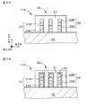
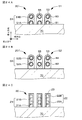
- FIGS. 3A and 3B are schematic partial cross-sectional views of the diode of Example 1 taken along arrows AA and BB in FIG. 2A, respectively.
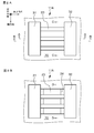
- 2A and 2B are a schematic layout view of the stacked structure of the diode, the first connection portion and the second connection portion, and a control electrode portion, an insulating layer, a first connection portion, and a second connection portion, respectively, of the first embodiment.
- FIG. 4 is a schematic layout diagram of two connection parts.
- FIGS. 3A and 3B are schematic partial cross-sectional views of the diode of Example 1 along arrows CC and DD in FIG. 2A, respectively.
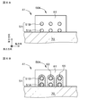
- FIGS. 6A and 6B are schematic layout diagrams of a channel portion and a source / drain region of the field-effect transistor according to the first embodiment, and schematic layout diagrams of a gate electrode, a gate sidewall, and a source / drain region, respectively.
- It is. 5A and 5B are a schematic partial cross-sectional view of a p-channel field-effect transistor along arrow AA in FIG. 4A, and a p-channel transistor along arrow BB in FIG. 4B, respectively.
- 3 is a schematic partial cross-sectional view of the field-effect transistor of FIG.
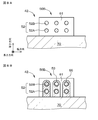
- FIGS. 6A and 6B are a schematic partial cross-sectional view of a p-channel field effect transistor along arrow CC in FIG.
- FIGS. 7A and 7B are schematic partial cross-sectional views of an n-channel field effect transistor taken along arrow AA in FIG. 4A, and an n-channel field effect transistor taken along arrow BB in FIG. 4B, respectively.
- 3 is a schematic partial cross-sectional view of the field-effect transistor of FIG.
- FIGS. 8A and 8B are a schematic partial cross-sectional view of an n-channel field effect transistor taken along the arrow CC in FIG. 4A, and an n-channel field effect transistor taken along the arrow DD in FIG. 4B, respectively.
- FIG. 9A and 9B are a schematic partial cross-sectional view of a first modification of the diode of the first embodiment, taken along the line BB in FIG. 2A, and a modification of the diode of the first embodiment, respectively.
- 2 is a schematic partial cross-sectional view similar to that taken along arrow AA in FIG. 2A.
- 10A and 10B are a schematic partial cross-sectional view of a third modification of the diode of the first embodiment, taken along the arrow AA of FIG. 2A, and a modification of the diode of the first embodiment, respectively.
- 4 is a schematic partial cross-sectional view similar to that taken along arrow AA in FIG. 2A.
- FIG. 11A and 11B are schematic partial cross-sectional views of a fifth modification of the diode according to the first embodiment, which are similar to the arrows AA in FIG. 2A, and arrows BB in FIG. 2A, respectively.
- FIG. 4 is a schematic partial cross-sectional view similar to FIG. 12A and 12B are schematic partial cross-sectional views of Modification Example 5 of the diode according to the first embodiment, taken along arrows CC and DD in FIG. 2A, respectively.
- FIGS. 13A and 13B are schematic partial cross-sectional views of the diode according to the second embodiment, taken along arrows CC in FIG. 2A and arrows DD in FIG. 2B, respectively.
- FIG. 14 is a schematic partial cross-sectional view of a fifth modification of the diode according to the first embodiment, which is similar to the arrow CC in FIG. 2A.
- FIG. 15 is a diagram for explaining an operation mechanism of the diode according to the first embodiment.
- FIG. 16 is a diagram for explaining the operation mechanism of the diode proposed in Non-Patent Document 1.
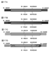
- 17A, 17B, 17C, and 17D show the results of a simulation of a diode having a structure similar to the diode of Example 1 and the potential distribution, electric field intensity distribution, and current density distribution in a stacked structure of the diode.
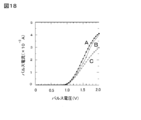
- FIG. FIG. 18 shows a diode having a structure similar to that of the diode of Example 1 shown in FIG.
- FIG. 9 is a diagram illustrating a result of simulating a pulse current flowing when a pulse voltage is applied.
- (A), (B), (C), (D), (E), (F), (G), (H) and (J) of FIG. 19 show the diode of Example 1 shown in FIG. 17A.
- FIG. 9 is a diagram illustrating a result of simulating a pulse current flowing when a pulse voltage is applied.
- (A), (B), (C), (D), (E), (F), (G), (H) and (J) of FIG. 19 show the diode of Example 1 shown in FIG. 17A.
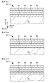
- FIG. 9 is a diagram showing a result of simulation of FIG. 20A, 20B, and 20C are schematic partial cross-sectional views of a base and the like for explaining the outline of the method for manufacturing the diode and the field-effect transistor according to the first embodiment.
- 21A, 21B, and 21C are schematic partial cross-sectional views of a base and the like for explaining the outline of the method for manufacturing the diode and the field-effect transistor according to the first embodiment.
- FIG. 22A, FIG. 22B, and FIG. 22C are schematic partial cross-sectional views of a base and the like for explaining the outline of the method for manufacturing the diode and the field-effect transistor of Example 1.
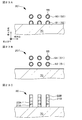
- 23A, 23B, and 23C are schematic partial cross-sectional views of a base and the like for explaining the outline of the method for manufacturing the diode and the field-effect transistor according to the first embodiment.
- 24A, 24B, and 24C are schematic partial cross-sectional views of a base and the like for explaining the outline of the method for manufacturing the diode and the field-effect transistor according to the first embodiment.
- FIG. 25A, FIG. 25B, and FIG. 25C are schematic partial cross-sectional views of a base and the like for explaining the outline of the method for manufacturing the diode and the field-effect transistor of Example 1.
- Example 1 diode according to first embodiment of present disclosure
- Example 2 diode according to second embodiment of present disclosure
- the laminated structure may be configured to be provided on a base.
- the control electrode portion is not formed on the bottom surface of the multilayer structure.
- the control electrode portion may further be formed over the bottom surface of the multilayer structure.
- the body may be configured to be provided above the base.
- the bottom surface of the laminated structure is not in contact with the substrate, the bottom surface of the control electrode portion is in contact with the substrate, or the bottom surface of the control electrode portion is located above the substrate, There is a gap between the bottom surface of the control electrode unit and the top surface of the base.
- the base is made of a silicon semiconductor substrate or an SOI (Si On Insulator) substrate, or a GOI ( A structure including a Ge On Insulator (SOGI) substrate and an SGOI (SiGe On Insulator) substrate can be employed.
- SOI Silicon On Insulator
- SOGI Ge On Insulator
- SGOI SiGe On Insulator
- the first connection portion and the second connection portion may be configured to be provided on a base. Can be.
- the region of the base on which the diode is provided has the second conductivity type, and the first connection portion and the control electrode portion are provided. And are electrically connected.
- the first conductivity type is p-type and the second conductivity type is n-type. It can be.
- the first structure is made of silicon-germanium (Si-Ge), and the second structure is Can be made of silicon (Si).
- the first structure may be made of germanium (Ge) or InGaAs, and the second structure may be made of silicon (Si).
- the first connection portion may be made of, for example, a material forming the first structure
- the second connection portion may be made of, for example, a material forming the second structure.
- the multilayer structure may have an intrinsic semiconductor region (intrinsic region), or may have a stacked structure.
- the structure may have an impurity concentration of 1 ⁇ 10 18 / cm 3 or less.
- a side surface of the control electrode portion facing the first connection portion, and a control electrode portion facing the second connection portion May be in a form in which an insulating layer (sidewall) is formed on the side surface.
- control electrode unit may be formed of TiN, TaN, Al, TiAl, or W.
- the first portion of the multilayer structure and the second portion of the multilayer structure may be in contact with each other.
- the number of laminated structures may be one or two or more. Further, the number of the first structures can be one or two or more, and the number of the second structures can also be one or two or more. The numbers of the first structures and the second structures may be the same or different.
- the lowermost layer of the laminated structure may be constituted by the first structure, or may be constituted by the second structure.
- one control electrode unit may be provided for the entire laminated structure, or the laminated structure of these may be provided. One control electrode unit may be provided for each of the structures.
- the semiconductor device may be configured to include the diodes according to the first and second aspects of the present disclosure and a field-effect transistor having a GAA structure.
- the field effect transistor has a plurality of channel portions having a nanowire structure or a nanosheet structure, a gate insulating film surrounding each channel portion, and a channel structure portion including a gate electrode surrounding at least a part of each gate insulating film. Having. At least two channel portions are juxtaposed in the thickness direction of the channel structure portion, and the lowermost channel portion is formed on the base or above the base. That is, the plurality of channel portions are spaced apart from each other in the thickness direction of the channel structure portion, and the space between the channel portions is filled with a gate insulating film and a gate electrode.
- the number of channel portions in the stacking direction of the channel structure portions of the field effect transistor may be two or more, and the number of channel portions in the direction orthogonal to the thickness direction of the channel structure portion (the width direction of the channel structure portion) is one. Alternatively, it may be two or more.
- the sum of the heights of the channel portions is the sum of the diameters or thicknesses of the materials (for example, Si, Si—Ge, Ge, and InGaAs) that form the nanowire structure or the nanosheet structure that forms the channel portion.
- At least a portion of the lowermost channel portion of the field-effect transistor is surrounded by the gate electrode, and the other channel portions may be surrounded by the gate electrode. That is, in the field effect transistor, between the channel portions, a gate insulating film surrounding the channel portion located below (ie, a gate insulating film formed on the outer peripheral portion of the channel portion), and A gate insulating film surrounding the located channel portion (ie, a gate insulating film formed on the outer peripheral portion of the channel portion) is formed, and a gate electrode is formed between these gate insulating films.
- the channel portion of the n-channel field-effect transistor is made of silicon (Si), and the channel portion of the p-channel field-effect transistor is made of silicon-germanium (Si-Ge), germanium (Ge), or InGaAs. can do. However, it is not limited to this.
- the channel portion of the n-channel type field effect transistor is made of silicon-germanium (Si-Ge), and the channel portion of the p-channel type field effect transistor is made of silicon (Si), germanium (Ge) or InGaAs.
- the channel portion of the n-channel type field effect transistor is made of germanium (Ge), and the channel portion of the p-channel type field effect transistor is made of silicon (Si), silicon-germanium (Si-Ge) or InGaAs.
- the channel portion of the n-channel field-effect transistor is made of InGaAs, and the channel portion of the p-channel field-effect transistor is made of silicon (Si), silicon-germanium (Si-Ge), or germanium (Ge). It can be in the form of
- the field effect transistor is an n-channel type or a p-channel type is determined, for example, by a work function value of a material forming a gate electrode.
- a work function value of a material forming a gate electrode for example, by a work function value of a material forming a gate electrode.
- the channel portion is made of Si
- TiN, TaN, Al, TiAl, and W can be used as a material forming the gate electrode.
- TiN and W can be used as a material forming the gate electrode.
- the voltage applied to the gate electrode of the field effect transistor may be, for example, 0.5 volt to 0.8 volt, but is not limited thereto.
- SiON and SiO 2 can be used, and a high dielectric constant material (a so-called High-k material) such as HfO 2 , HfAlON, and Y 2 O 3 can be used. it can.
- both ends of the nanowire structure having a diameter of, for example, 5 nm to 10 nm and made of, for example, Si or Si—Ge are connected to the first connection portion and the second connection portion.
- a material having a width ⁇ thickness of, for example, (10 nm to 50 nm) ⁇ (5 nm to 10 nm) and a substantially rectangular cross section made of, for example, Si or Si—Ge is used. Are in contact with the first connection portion and the second connection portion.
- both ends of the nanowire structure having a diameter of, for example, 5 nm to 10 nm and made of, for example, Si or Si—Ge are connected to the source forming the field effect transistor. / Drain region.
- a nanosheet structure constituting a channel portion of a field-effect transistor a cross-sectional shape made of, for example, Si or Si—Ge having a width ⁇ thickness of, for example, (10 nm to 50 nm) ⁇ (5 nm to 10 nm) is substantially used. Both ends of the rectangular material are supported by source / drain regions forming a field effect transistor. Whether the structure is a nanowire structure or a nanosheet structure depends on the thickness and width of the materials constituting these structures.
- examples of the base include a silicon semiconductor substrate, an SOI substrate, a GOI substrate, and an SGOI substrate.
- the laminated structure and the channel portion preferably have crystallinity, but may be made of polycrystal, or may be made of amorphous in some cases.
- Examples of a method for forming the laminated structure and the channel portion include an epitaxial CVD method, a plasma CVD method, and an atomic layer deposition method (ALD method).
- a digital circuit such as a logic circuit, an SRAM circuit, or a CMOS circuit can be constituted by a diode or a field-effect transistor, and a logic circuit for controlling an imaging device and a driving of an imaging element (a light receiving element) included in the imaging apparatus
- the circuit can be composed of a diode or a field-effect transistor, and the CPU or GPU can be composed of a diode or a field-effect transistor, but is not limited to these.
- Example 1 relates to the diode according to the first embodiment of the present disclosure.
- FIG. 2A shows a schematic layout diagram of the stacked structure of the diode, the first connection portion, and the second connection portion of the first embodiment, and schematically shows the control electrode portion, the insulating layer, the first connection portion, and the second connection portion.
- FIG. 2B shows a schematic layout diagram
- FIG. 1A shows a schematic partial cross-sectional view of the diode of Example 1 along arrow AA in FIG. 2A
- FIG. 2A schematically shows a diode along arrow BB in FIG. 2A.
- 1B a schematic partial cross-sectional view along arrow CC of FIG. 2A is shown in FIG.
- FIG. 3A shows a schematic layout of a channel portion and a source / drain region of the field-effect transistor in Example 1
- FIG. 4B shows a schematic layout of a gate electrode, a gate sidewall, and a source / drain region.
- FIG. 5A and FIG. 7A show schematic partial cross-sectional views of p-channel and n-channel field-effect transistors taken along the arrow AA in FIG. 4A, and show the cross-section taken along the arrow BB in FIG. 4B.
- 5B and 7B are schematic partial cross-sectional views of p-channel and n-channel field-effect transistors, and are schematic diagrams of p-channel and n-channel field-effect transistors along arrows CC in FIG. 4A.
- 6A and 8A show typical partial cross-sectional views
- FIG. 6B and FIG. 6B show schematic partial cross-sectional views of p-channel and n-channel field effect transistors along arrows DD in FIG. 4B.
- FIG 8B shows schematic partial cross-sectional views of p-channel and n-channel field effect transistors along arrows DD in FIG. 4B.
- the diode according to the first embodiment or a second embodiment described below Laminated structures 20, 25, A first connection portion 31 provided at one end in the length direction of the laminated structures 20 and 25; A second connecting portion 32 provided at the other longitudinal end of the laminated structures 20 and 25; With The laminated structures 20 and 25 include first structures 21 and 26 having a nanowire structure or a nanosheet structure (specifically, for example, a nanowire structure), and a material forming the first structures 21 and 26.
- the first connection portion 31 has a first conductivity type (specifically, for example, a p-type)
- the second connection portion 32 has a second conductivity type (specifically, for example, n-type) different from the first conductivity type.
- the diode according to the first embodiment further includes a control electrode unit 23 formed at least from the top to the side surface of the multilayer structure 20 so as to be separated from the first connection unit 31 and the second connection unit 32.
- the first connection portion 31 and the control electrode portion 23 or the second connection portion 32 and the control electrode portion 23 are electrically connected.
- the diode 11 ⁇ / b> A of the first embodiment further includes a control electrode unit 23 formed to be spaced apart from the first connection unit 31 and the second connection unit 32 from the top to the side surface of the multilayer structure 20.
- the first connection part 31 and the control electrode part 23 are electrically connected. That is, the diode of the first embodiment has a so-called MOS diode structure.
- the laminated structures 20 and 25 are provided on the base 70. In such a configuration, the bottom surfaces of the laminated structures 20 and 25 are in contact with the base 70. In the diode 11 ⁇ / b> A of the first embodiment, the control electrode part 23 is not formed on the bottom surface of the multilayer structure 20.
- the laminated structures 20 and 25 specifically include two first structures 21A, 21B, 26A and 26B and two second structures 22A, 22B, 27A, and 27B are alternately stacked in the thickness direction and have a four-layer configuration, and the thickness (thickness of each layer) and width of each structure are, for example, 8 nm and 8 nm.
- One end in the length direction of the stacked structures 20 and 25 is in contact with the first connection portion 31, and the other end is in contact with the second connection portion 32.
- the lowermost layer of the laminated structures 20 and 25 may be constituted by the first structures 21A and 26A or may be constituted by the second structures 22A and 27A. It is composed of structures 21A and 26A.
- the base 70 is made of a silicon semiconductor substrate.
- the first connection portion 31 and the second connection portion 32 are provided on the base 70.
- the first structure 21 and the first connection portion 31 are made of silicon-germanium (Si-Ge), and the second structure 22 and the second connection portion 32 are formed. Is made of silicon (Si).
- the side surface of the control electrode portion 23 facing the first connection portion 31 and the side surface of the control electrode portion 23 facing the second connection portion 32 are made of, for example, HfO 2.
- a layer (sidewall) 24 is formed, and the control electrode portion 23 is made of TiN, TaN, Al, TiAl, or W, and specifically, is made of, for example, TiN.
- the length of the control electrode unit 23 is, for example, 0.1 ⁇ m, and the distance between the first connection unit 31 and the second connection unit 32 is 0.14 ⁇ m.
- the stacked structure 20 has an intrinsic semiconductor region (intrinsic region), or the stacked structure 20 has an impurity concentration of 1 ⁇ 10 18 / cm 3 or less.
- the first structure 21 and the second structure 22 are made of an intrinsic semiconductor, or have an impurity concentration of 1 ⁇ 10 18 / cm 3 or less.
- the semiconductor device includes the diode of Example 1 or Example 2 and a GAA structure (a gate electrode surrounds an outer peripheral portion of a channel portion in a continuous state without a break. And a so-called omega ( ⁇ ) structure (a mode in which the gate electrode surrounds the outer peripheral portion of the channel portion but partially surrounds it).
- GAA structure a gate electrode surrounds an outer peripheral portion of a channel portion in a continuous state without a break.
- omega ( ⁇ ) structure a mode in which the gate electrode surrounds the outer peripheral portion of the channel portion but partially surrounds it.
- An effect transistor 41 is provided.
- the p-channel field effect transistor 41 includes a plurality of channel portions 51 (51A, 51B) having a nanowire structure or a nanosheet structure, a gate insulating film 55 surrounding each channel portion 51 (51A, 51B), and a gate insulating film.
- a channel structure 50A having a gate electrode 53 surrounding at least a part of the film 55 is provided.
- the n-channel type field effect transistor 42 has a plurality of channel portions 52 (52A, 52B) having a nanowire structure or a nanosheet structure, a gate insulating film 55 surrounding each channel portion 52 (52A, 52B), and A channel structure 50B having a gate electrode 53 surrounding at least a part of the gate insulating film 55 is provided.
- At least two channel portions 51 and 52 are formed in the thickness direction of the channel structure portion 50, and the lowermost channel portions 51 and 52 are formed on the base 70 or above the base 70. I have.
- two channel portions 51 (51A, 51B) are formed in the thickness direction of the channel structure portion 50A, and the lowermost channel portion 51A is formed on the base 70. I have.
- the gate electrode 53 is not formed between the lowermost channel portion 51A and the base 70 ( ⁇ structure).
- two channel portions 52 (52A, 52B) are formed in the thickness direction of the channel structure portion 50B, and the lowermost channel portion 52A is formed above the base 70.
- a gate electrode 53 is formed between the lowermost channel portion 52A and the base 70 (GAA structure).
- the plurality of channel portions 51 and 52 are spaced apart from each other in the thickness direction of the channel structure portions 50A and 50B, and a gate insulating film is provided between the channel portions 51 and 52 and the channel portions 51 and 52. 55 and the gate electrode 53.
- One end in the length direction of the channel portions 51 and 52 is in contact with one source / drain region 61, and the other end is in contact with the other source / drain region 62.
- a gate sidewall 54 made of, for example, HfO 2 is formed on a side surface of the gate electrode 53 facing the source / drain regions 61 and 62.
- the lowermost channel portion of the field effect transistor is surrounded by the gate electrode, and the other channel portions are surrounded by the gate electrode.
- a part of the outer peripheral portion of the lowermost channel portion 51A constituting the field effect transistor 41 is not surrounded by the gate electrode 53.
- a part of the outer peripheral portion of the lowermost channel portion 52A constituting the field effect transistor 42 is surrounded by the gate electrode 53.
- the channel portion 51 (51A, 51B) of the field effect transistor 41 of the first embodiment is made of silicon-germanium (Si-Ge), and the channel portion 52 (52A, 52B) of the field effect transistor 42 is made of silicon (Si).
- the material forming the gate electrodes 53 of the field effect transistors 41 and 42 is, for example, TiN, and the gate insulating film 55 has a laminated structure of SiON and HfO 2 .
- FIG. 15 is a diagram illustrating the operation mechanism of the diode 11A according to the first embodiment
- FIG. 16 is a diagram illustrating the operation mechanism of the diode having the GAA structure proposed in Non-Patent Document 1 described above.
- . 15 and 16 are schematic cross-sectional views similar to FIG. 1A.
- “(1) position” is a diagram illustrating a change in potential in the second structure 22B
- “(2) position” is a diagram illustrating a change in potential in the first structure 21B.
- V> V bi means that a voltage (for example, +1.0 volt) higher than the substrate bias V bi (specifically, 0 volt) is applied to the first connection portion 31 and the control electrode portion 23, and the second connection portion The potential when the part 32 is grounded (0 volt is applied) is shown.
- FIGS. 25B and 25C The outline of the method of manufacturing the diode and the field-effect transistor according to the first embodiment will be described with reference to FIGS. 25B and 25C.
- 20A, 20B, 20C, 21A, 21B, 21C, 22A, 22B, 22C, 23A, 23B, 23C, 24A, 24B, and 24C are shown in FIGS.
- FIG. 25A, FIG. 25B, and FIG. 25C are schematic partial cross-sectional views of a base and the like similar to those taken along arrows CC in FIG. 4A.
- FIG. 3 is a schematic partial cross-sectional view of a substrate and the like.
- an element isolation region (not shown) for a diode and a field effect transistor is formed on a desired region of the base 70, and then the first semiconductor layer 81 (the first structure 21A and the first structure 21A) made of Si—Ge is formed.
- a third semiconductor layer 83 made of Si-Ge (a semiconductor layer forming the first structure 21B and the channel portion 51B of the p-channel field effect transistor 41), and a fourth semiconductor layer 83 made of Si.
- the semiconductor layer 84 (which is a semiconductor layer forming the channel portion 52B of the second structure 22B and the n-channel type field effect transistor 42) is sequentially formed. , For example, it is formed on the basis of the epitaxial CVD method.
- the first semiconductor layer 81, the second semiconductor layer 82, the third semiconductor layer 83, and the fourth semiconductor layer 84 are made of an intrinsic semiconductor, or have an impurity concentration of 1 ⁇ 10 18 / cm 3 or less.
- the laminated structure 20 and the laminated structures 20 ′ and 20 ′′ (the channel structure portions 50 A and 50 B formed of the first semiconductor layer 81, the second semiconductor layer 82, the third semiconductor layer 83, and the fourth semiconductor layer 84 are formed.
- the substrate 70 on which the diode 11A is to be formed and on the substrate 70 on which the field-effect transistor is to be formed are formed.
- 20A, 20B and 20C can be obtained.
- Step-120A the laminated structure 20 and the laminated structure 20 ′′ for forming the channel structure 50B of the n-channel type field effect transistor 42 are covered with an appropriate mask layer, and the p-type field effect transistor 41 is
- the laminated structure 20 ′ for forming the channel structure 50A is exposed, and an etching resist 91 having a desired resist pattern is formed (see FIG. 21A), and the fourth semiconductor layer 84 and the third semiconductor layer 84 are formed. Pattern the semiconductor layer 83, the second semiconductor layer 82, and the first semiconductor layer 81. A nanowire structure or a nanosheet structure is obtained depending on the width of the etching resist 91. Thus, FIG. Can be obtained.
- the second semiconductor layer 82 and the fourth semiconductor layer 84 made of Si are formed by using an etchant having an etching selectivity with respect to the material (Si—Ge) forming the first semiconductor layer 81 and the third semiconductor layer 83. Remove. Both ends of the channel portion 52 having the nanowire structure are supported by the support portion having the laminated structure 20 ′. After that, the etching resist 91 is removed. Thus, the structure shown in FIG. 21C can be obtained.
- Step-130A Thereafter, the components of the channel structure 50A of the p-channel type field effect transistor 41 are covered with an appropriate mask layer to form the laminated structure 20 and the channel structure 50B of the n-channel type field effect transistor 42. Then, an etching resist 92 having a desired resist pattern is formed (see FIG. 22A), and the fourth semiconductor layer 84, the third semiconductor layer 83, and the second semiconductor are formed. Pattern the layer 82 and the first semiconductor layer 81. A nanowire structure or a nanosheet structure is obtained depending on the width of the etching resist 92. Thus, the structure shown in FIGS. Obtainable.
- Step-130B Next, the first semiconductor layer 81 and the third semiconductor layer 83 made of Si—Ge are formed using an etchant having an etching selectivity with respect to the material (Si) forming the second semiconductor layer 82 and the fourth semiconductor layer 84. Remove. Both ends of the channel portion 51 composed of the nanowire structure are supported by the support composed of the laminated structure 20 ′′. Thereafter, the etching resist 92 is removed. Thus, the structure shown in FIG. 22C can be obtained.
- a gate insulating film 55 is formed in the channel portions 51 and 52. Specifically, first, a resist layer (not shown) having a desired resist pattern is formed, and then thermal oxidation is performed on the channel portions 51 and 52 to form a part of the gate insulating film made of SiON. I do. By performing the thermal oxidation treatment, the cross-sectional shapes of the channel portions 51 and 52 having the nanowire structure become circular. Next, the rest of the gate insulating film made of HfO 2 is formed on the gate insulating film based on the ALD method. Thus, the structure shown in FIGS. 23A and 23B can be obtained.
- the control electrode portion 23 is formed on a part of the laminated structure 20 constituting the diode 11A based on a CVD method, a lithography technique, and an etching technique.
- the gate electrodes 53 of the p-channel field-effect transistor 41 and the n-channel field-effect transistor 42 are formed based on a CVD method, a lithography technique, and an etching technique (see FIGS. 24A, 24B, and 24C).
- an insulating layer (sidewall) 24 and a gate sidewall 54 are formed by a known method.
- a first connection part 31, a second connection part 32, and source / drain regions 61 and 62 are formed. More specifically, the support portion composed of the laminated structures 20 ′ and 20 ′′ supporting both ends of the channel portions 51 and 52 is removed based on the lithography technique and the etching technique, and unnecessary portions are removed from the laminated structure 20. Is removed based on the lithography technique and the etching technique to expose the base 70. Then, a region other than the region of the base 70 where the first connection portion 31 is to be formed is covered with a mask layer (not shown) made of, for example, SiN.
- the mask layer is removed.
- a region other than the region of the substrate 70 where the source / drain regions 61 and 62 are to be formed is covered with another mask layer (not shown) made of, for example, SiN.
- the mask layer is removed after forming the second connection portion 32 and the source / drain regions 61 and 62 made of Si containing an n-type impurity on the base 70.
- the semiconductor device has a nanowire structure.
- the diode 11A and the field effect transistors 41 and 42 can be obtained, and further, an interlayer insulating layer is formed on the entire surface, and is located above the first connection portion 31, the second connection portion 32, and the control electrode portion 23.
- An opening may be formed in the interlayer insulating layer, and a connection hole, a wiring, and a connecting portion (a connecting portion for connecting the first connecting portion 31 and the control electrode portion 23) may be formed from inside the opening to over the interlayer insulating layer.
- an opening may be formed in the interlayer insulating layer located above the gate electrode 53 and the source / drain regions 61 and 62, and a connection hole and a wiring may be formed over the inside of the opening and over the interlayer insulating layer.
- a diode having a structure similar to the diode of Example 1 shown in FIG. 17A (referred to as a “diode for simulation” for convenience), and a potential distribution, an electric field intensity distribution, and a current density in a laminated structure of the diode for simulation.
- the results of simulating the distribution are shown in FIGS. 17B, 17C and 17D.
- the simulation diode includes a first connection portion 31 made of Si-Ge, a second connection portion 32 made of Si, one first structure 21 made of Si-Ge, and one second structure 22 made of Sie. It comprises a laminated structure 20 in which a total of two layers are laminated, and a control electrode portion 23 surrounding the outer periphery of the laminated structure 20.
- FIG. 18 shows a simulation result of a pulse current flowing when a pulse voltage is applied to a diode (referred to as “diode of Comparative Example 1B” for convenience).
- 18B shows the result of the diode for simulation
- FIG. 18A shows the result of the diode of Comparative Example 1A
- FIG. 18C shows the result of the diode of Comparative Example 1B. Show. It was confirmed that the diode for simulation had almost the same operating characteristics as the diode of Comparative Example 1A, and had characteristics superior to those of the diode of Comparative Example 1B.
- FIG. 19 shows the simulation results of the potential distribution, the electric field intensity distribution, and the current density distribution in the stacked structure of the simulation diode, the diode of Comparative Example 1A, and the diode of Comparative Example 1B.
- the diode according to the first embodiment or a second embodiment described later has a stacked structure in which the first structure and the second structure having the nanowire structure or the nanosheet structure are alternately stacked in the thickness direction.
- it is possible to suppress a decrease in the current that can be passed through the diode as much as possible.
- it has a high affinity with a manufacturing process of a field-effect transistor having a GAA structure. That is, the diode according to the first embodiment or a second embodiment described later can be manufactured in the same process as a field-effect transistor having a GAA structure, for example.
- Example 1 since the control electrode portion is provided, electrons are injected from the gate electrode into the multilayer structure, so that the conduction band and the valence band in the multilayer structure are depressed, Even if the laminated structure has an intrinsic semiconductor region (intrinsic region), or the impurity concentration of the laminated structure is 1 ⁇ 10 18 / cm 3 or less, the potential becomes substantially the same as that of the first connection portion, and Current can flow as
- the diode having the GAA structure proposed in Non-Patent Document 1 described above and the diode of Example 1 will be compared below.
- the cross-sectional area of the laminated structure 20 including the two first structures 21 and the two second structures 22, that is, the cross-sectional area of the diode according to the first embodiment through which a current can flow is 4a 2 .
- a cross-sectional area having a width a and a height 4a is occupied by two structures.
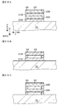
- FIG. 9A is a schematic partial cross-sectional view of a modification 1 (diode 11B) of the diode according to the first embodiment, which is similar to that taken along arrow BB in FIG. 2A.
- the second connection part 32 and the control electrode part 23 are electrically connected.
- FIG. 9B is a schematic partial cross-sectional view of a second modification (diode 11C) of the diode according to the first embodiment, similar to the arrow AA in FIG. 2A.
- the region of the base 70 on which the diode 11C is provided has the second conductivity type (specifically, n + ), and the first connection portion 31 and the control electrode portion 23 The second connection part 32 and the control electrode part 23 are electrically connected.
- the upper region of the base 70 on which the diode 11C is provided includes an n + region 71, and the first connection portion 31 and the n + region 71 also form a diode. With such a structure, the number of current paths can be increased, and the current that can flow through the diode can be increased.
- FIG. 10A is a schematic partial cross-sectional view of a third modification (diode 11D) of the diode according to the first embodiment, which is similar to the arrow AA in FIG. 2A.
- the base is made of the SOI substrate 72.
- the diode 11D is provided on a silicon layer 73 constituting the SOI substrate 72.
- FIG. 10B is a schematic partial cross-sectional view of a fourth modification (diode 11E) of the diode according to the first embodiment, which is similar to the arrow AA in FIG. 2A.
- the silicon layer 74 constituting the portion of the base 72 on which the diode 11E is provided has the second conductivity type (specifically, n + ).
- the control electrode section 23 is electrically connected, or the second connection section 32 and the control electrode section 23 are electrically connected.
- the base is made of SOI substrate 72, and diode 11E is provided on n + silicon layer 74 constituting SOI substrate 72.
- the first connection portion 31 and the n + silicon layer 74 also constitute a diode. With such a structure, the number of current paths can be increased, and the current that can flow through the diode can be increased.
- FIG. 11A is a schematic partial cross-sectional view of Modification Example 5 (diode 11F) of the diode according to Example 1 taken along arrow AA in FIG. 2A, taken along arrow BB in FIG. 2A.
- FIG. 11B shows a similar schematic partial cross-sectional view
- FIGS. 12A and 12B show similar schematic partial cross-sectional views taken along arrows CC and DD in FIG. 2A, respectively.
- the control electrode portion 23 is formed over the bottom surface of the multilayer structure 20.
- the laminated structure 20 is provided above the base 70.
- the bottom surface of the laminated structure 20 is not in contact with the substrate 70, and the bottom surface of the control electrode portion 23 is in contact with the substrate 70, or, as shown in the drawing, Is located above the base 70, and there is a gap between the bottom of the control electrode unit 23 and the top of the base 70.
- the lowermost layer of the laminated structure 20 is constituted by the second structure 22A, the number of the first structures 21 is 1, and the number of the second structures 22 is 2, but the present invention is not limited thereto. is not.
- Such a structure can be obtained by forming a sacrifice layer instead of the above-described first semiconductor layer 81 and removing the sacrifice layer from the stacked structure 20 in the same step as [Step-130B].
- Example 2 relates to the diode according to the second aspect of the present disclosure.
- FIGS. 13A and 13B are schematic partial cross-sectional views of the diode of Example 2 taken along arrows CC in FIG. 2A and arrows DD in FIG. 2B.
- the control electrode portion 23 is not provided, and the first portion 25A of the multilayer structure 25 that is in contact with the first connection portion 31 is the first conductive portion 25A.
- the second portion 25B of the multilayer structure 25 that is in contact with the second connection portion 32 has a second conductivity type (specifically, for example, n-type). .
- the first portion 25A of the multilayer structure 25 is in contact with the second portion 25B of the multilayer structure 25.
- the first portion 25A can be provided by ion-implanting a p-type impurity
- the second portion 25B can be provided by ion-implanting an n-type impurity.
- the configuration and structure of the diode of the second embodiment can be the same as the configuration and structure of the diode of the first embodiment.
- the configurations and structures of Modification 2, Modification 3, Modification 4, and Modification 5 of Embodiment 1 can be appropriately applied to the diode of Embodiment 2.
- the difference in the work function between the first structure 26 (26B) made of Si—Ge and the second structure 27 (27A, 27B) made of Si is 0.1 eV.
- the potential difference between the first connection portion 31 and the second connection portion 32 when operating as a diode absorbs the difference in the work function value, and the diode operation as a whole is reduced. It is possible. Further, since the first structure 26 and the second structure 27 do not separately operate as a diode but operate as a single diode, the current path can be doubled and the current that can flow through the diode can be increased. Can be.
- the present disclosure has been described based on the preferred embodiments, the configurations and structures of the diodes and the field-effect transistors described in the embodiments, the materials for forming the diodes and the field-effect transistors, and the methods of manufacturing the diodes and the field-effect transistors are merely examples. Yes, and can be changed as appropriate. The order of the steps in the method for manufacturing a diode or a field effect transistor can be changed as appropriate as desired.
- the laminated structure and the channel portion have been described based solely on the nanowire structure. However, a nanosheet structure may be used.
- a GOI substrate or an SGOI substrate can be used instead of a silicon semiconductor substrate or an SOI substrate.
- the element isolation region can be formed, for example, in [Step-120A] or [Step-130A].
- FIG. 14 which is a schematic partial cross-sectional view similar to that taken along arrow AA in FIG. 2A
- the first connecting portion 31 in contact with one end in the longitudinal direction of the laminated structures 20 and 25 is
- the second connecting portions 32 having protrusions with respect to the first structures 21 and 26 and the second structures 22 and 27 and being in contact with the other ends in the length direction of the laminated structures 20 and 25 are formed by the first structure 21 and 26 and the second structures 22 and 27 may have a projection.
- the first structures 21 and 26 and the second structures 22 and 27 are etched.
- the first structures 21 and 26 and the second structures 22 and 27 can have such a shape.
- the shapes of the first structures 21 and 26 and the second structures 22 and 27 obtained by etching are different from the plane orientations of the first structures 21 and 26 and the second structures 22 and 27 and the first structures 21 and 26. 26 and the direction in which the second structures 22 and 27 extend.
- the Si—Ge layer is formed by forming an upper Si—Ge layer on a lower Si layer and performing an oxidizing process so that the upper Si—Ge layer becomes SiO 2 and the lower Si layer becomes a Si—Ge layer. And can be obtained by the following process.
- the present disclosure may have the following configurations.
- the laminated structure has a first structure having a nanowire structure or a nanosheet structure, and a second structure having a nanowire structure or a nanosheet structure formed of a material different from a material forming the first structure.
- the first connection portion has a first conductivity type
- the second connection portion has a second conductivity type different from the first conductivity type
- a control electrode portion formed at least from the top portion to the side surface of the multilayer structure so as to be separated from the first connection portion and the second connection portion; A diode in which the first connection portion and the control electrode portion or the second connection portion and the control electrode portion are electrically connected.
- [A04] The diode according to [A03], wherein the laminated structure is provided above the base.
- [A05] The diode according to any one of [A02] to [A04], wherein the base is made of a silicon semiconductor substrate or an SOI substrate.
- [A06] The diode according to any one of [A02] to [A05], wherein the first connection portion and the second connection portion are provided on a base.
- the region of the base on which the diode is provided has the second conductivity type, The first connection portion and the control electrode portion are electrically connected, or the second connection portion and the control electrode portion are electrically connected to any one of [A02] to [A06].
- the first conductivity type is a p-type, The diode according to any one of [A01] to [A07], wherein the second conductivity type is an n-type.
- the first structure is made of silicon-germanium, The diode according to any one of [A01] to [A08], wherein the second structure is made of silicon.
- the diode according to any one of [A01] to [A09], wherein the impurity concentration of the multilayer structure is 1 ⁇ 10 18 / cm 3 or less.
- An insulating layer is formed on a side surface of the control electrode portion facing the first connection portion and a side surface of the control electrode portion facing the second connection portion.
- [A01] to [A11] Item 2. The diode according to item 1.
- [A13] The diode according to any one of [A01] to [A12], wherein the control electrode portion is made of TiN, TaN, Al, TiAl or W.
- Second Embodiment >> Laminated structure, A first connection portion provided at one end of the laminated structure in the length direction, and A second connection portion provided at the other end in the length direction of the multilayer structure;
- the laminated structure has a first structure having a nanowire structure or a nanosheet structure, and a second structure having a nanowire structure or a nanosheet structure made of a material different from a material forming the first structure.
- the first connection portion has a first conductivity type
- the second connection portion has a second conductivity type different from the first conductivity type
- a first portion of the multilayer structure contacting the first connection portion has a first conductivity type
- a second portion of the stacked structure contacting the second connection portion is a diode having the second conductivity type.
- [C02] The length of the upper surface of the first structure or the second structure L T, the length of the lower surface of the first structure or the second structure L B, thickness of the first structure or the second structure When the length of the central part in the vertical direction is L C , L T > L C and L B > L C
- the diode according to [C01] satisfying the following.
- 11A, 11B, 11C, 11D, 11E, 11F, 12 Diode, 20, 25: Stacked structure, 21, 21A, 21B, 26, 26B: First structure, 22, 22A, 22B , 27, 27A, 27B ... second structure, 23 ... control electrode part, 24 ... insulating layer (sidewall), 25A ... first part of laminated structure, 25B ... 2nd part of laminated structure, 31 ... 1st connection part, 32 ... 2nd connection part, 41, 42 ... Field-effect transistor, 50A, 50B ... Channel structure part, 51, 51A , 51B, 52, 52A, 52B ... channel portion, 53 ... gate electrode, 54 ... gate side wall, 55 ...
- gate insulating film 61, 62 ... source / drain region, 70 ... ..Substrate, 71... It takes n + layer, 72 ... SOI substrate, 73 a silicon layer in ... SOI substrate, n + silicon layer at 74 ... SOI substrate, 81 ... first semiconductor layer, 82 ... second semiconductor Layer, 83: third semiconductor layer, 84: fourth semiconductor layer, 91, 92: resist for etching
Landscapes
- Electrodes Of Semiconductors (AREA)
- Metal-Oxide And Bipolar Metal-Oxide Semiconductor Integrated Circuits (AREA)
- Thin Film Transistor (AREA)
- Chemical & Material Sciences (AREA)
- Engineering & Computer Science (AREA)
- Crystallography & Structural Chemistry (AREA)
- Nanotechnology (AREA)
Abstract
Description
積層構造体、
積層構造体の長さ方向の一端に設けられた第1接続部、及び、
積層構造体の長さ方向の他端に設けられた第2接続部、
を備えており、
積層構造体は、ナノワイヤー構造又はナノシート構造を有する第1構造体、及び、第1構造体を構成する材料とは異なる材料から構成されたナノワイヤー構造又はナノシート構造を有する第2構造体が、厚さ方向に、交互に積層されて成り、
第1接続部は、第1導電型を有し、
第2接続部は、第1導電型とは異なる第2導電型を有する。
1.本開示の第1の態様~第2の態様に係るダイオード、全般に関する説明
2.実施例1(本開示の第1の態様に係るダイオード)
3.実施例2(本開示の第2の態様に係るダイオード)
4.その他
本開示の第1の態様~第2の態様に係るダイオードにおいて、積層構造体は基体の上に設けられている構成とすることができる。このような構成にあっては、積層構造体の底面は基体と接しているので、制御電極部は積層構造体の底面に形成されていない。
[a]nチャネル型の電界効果トランジスタのチャネル部は、シリコン-ゲルマニウム(Si-Ge)から成り、pチャネル型の電界効果トランジスタのチャネル部は、シリコン(Si)、ゲルマニウム(Ge)又はInGaAsから成る形態とすることができるし、
[b]nチャネル型の電界効果トランジスタのチャネル部は、ゲルマニウム(Ge)から成り、pチャネル型の電界効果トランジスタのチャネル部は、シリコン(Si)、シリコン-ゲルマニウム(Si-Ge)又はInGaAsから成る形態とすることができるし、
[c]nチャネル型の電界効果トランジスタのチャネル部は、InGaAsから成り、pチャネル型の電界効果トランジスタのチャネル部は、シリコン(Si)、シリコン-ゲルマニウム(Si-Ge)又はゲルマニウム(Ge)から成る形態とすることができる。
積層構造体20,25、
積層構造体20,25の長さ方向の一端に設けられた第1接続部31、及び、
積層構造体20,25の長さ方向の他端に設けられた第2接続部32、
を備えており、
積層構造体20,25は、ナノワイヤー構造又はナノシート構造(具体的には、例えば、ナノワイヤー構造)を有する第1構造体21,26、及び、第1構造体21,26を構成する材料とは異なる材料から構成されたナノワイヤー構造又はナノシート構造(具体的には、例えば、ナノワイヤー構造)を有する第2構造体22,27が、厚さ方向に、交互に積層されて成り、
第1接続部31は第1導電型(具体的には、例えば、p型)を有し、
第2接続部32は、第1導電型とは異なる第2導電型(具体的には、例えば、n型)を有する。
先ず、基体70の所望の領域の上に、ダイオード及び電界効果トランジスタのための素子分離領域(図示せず)を形成した後、Si-Geから成る第1半導体層81(第1構造体21A及びpチャネル型の電界効果トランジスタ41のチャネル部51Aを構成する半導体層である)、Siから成る第2半導体層82(第2構造体22A及びnチャネル型の電界効果トランジスタ42のチャネル部52Aを構成する半導体層である)、Si-Geから成る第3半導体層83(第1構造体21B及びpチャネル型の電界効果トランジスタ41のチャネル部51Bを構成する半導体層である)、Siから成る第4半導体層84(第2構造体22B及びnチャネル型の電界効果トランジスタ42のチャネル部52Bを構成する半導体層である)を、順次、例えば、エピタキシャルCVD法に基づき形成する。第1半導体層81、第2半導体層82、第3半導体層83及び第4半導体層84は、真性半導体から成り、あるいは又、不純物濃度は1×10¹⁸/cm3以下である。
次に、第1半導体層81、第2半導体層82、第3半導体層83及び第4半導体層84から成る積層構造体20及び積層構造体20’,20”(チャネル構造部50A,50Bを形成するための積層構造体)のそれぞれを、周知のリソグラフィ技術及びエッチング技術に基づき、ダイオード11Aを形成すべき基体70の上、及び、電界効果トランジスタを形成すべき基体70の上に形成する。こうして、図20A、図20B及び図20Cに示す構造を得ることができる。
その後、積層構造体20、及び、nチャネル型の電界効果トランジスタ42のチャネル構造部50Bを形成するための積層構造体20”を適切なマスク層で被覆し、pチャネル型の電界効果トランジスタ41のチャネル構造部50Aを形成するための積層構造体20’を露出した状態とする。そして、所望のレジストパターンを有するエッチング用レジスト91を形成し(図21A参照)、第4半導体層84、第3半導体層83、第2半導体層82及び第1半導体層81をパターニングする。エッチング用レジスト91の幅に依存して、ナノワイヤー構造が得られ、あるいは又、ナノシート構造が得られる。こうして、図21Bに示す構造を得ることができる。
次いで、第1半導体層81及び第3半導体層83を構成する材料(Si-Ge)に対してエッチング選択比を有するエッチャントを用いて、Siから成る第2半導体層82及び第4半導体層84を除去する。ナノワイヤー構造から成るチャネル部52の両端は、積層構造体20’から成る支持部によって支持されている。その後、エッチング用レジスト91を除去する。こうして、図21Cに示す構造を得ることができる。
その後、pチャネル型の電界効果トランジスタ41のチャネル構造部50Aの構成要素を適切なマスク層で被覆し、積層構造体20、及び、nチャネル型の電界効果トランジスタ42のチャネル構造部50Bを形成するための積層構造体20”を露出した状態とする。そして、所望のレジストパターンを有するエッチング用レジスト92を形成し(図22A参照)、第4半導体層84、第3半導体層83、第2半導体層82及び第1半導体層81をパターニングする。エッチング用レジスト92の幅に依存して、ナノワイヤー構造が得られ、あるいは又、ナノシート構造が得られる。こうして、図22B及び図23Cに示す構造を得ることができる。
次いで、第2半導体層82及び第4半導体層84を構成する材料(Si)に対してエッチング選択比を有するエッチャントを用いて、Si-Geから成る第1半導体層81及び第3半導体層83を除去する。ナノワイヤー構造から成るチャネル部51の両端は、積層構造体20”から成る支持部によって支持されている。その後、エッチング用レジスト92を除去する。こうして、図22Cに示す構造を得ることができる。
その後、チャネル部51,52にゲート絶縁膜55を形成する。具体的には、先ず、所望のレジストパターンを有するレジスト層(図示せず)を形成した後、チャネル部51,52に熱酸化処理を行うことで、SiONから成るゲート絶縁膜の一部を形成する。熱酸化処理を行うことで、ナノワイヤー構造から成るチャネル部51,52の断面形状は円形となる。次いで、ゲート絶縁膜の上に、ALD法に基づき、HfO2から成るゲート絶縁膜の残部を形成する。こうして、図23A及び図23Bに示す構造を得ることができる。
次に、ダイオード11Aを構成する積層構造体20の一部に制御電極部23を、CVD法、リソグラフィ技術及びエッチング技術に基づき形成する。併せて、pチャネル型の電界効果トランジスタ41及びnチャネル型の電界効果トランジスタ42のゲート電極53を、CVD法、リソグラフィ技術及びエッチング技術に基づき形成する(図24A、図24B及び図24C参照)。その後、絶縁層(サイドウオール)24、ゲートサイドウオール54を周知の方法で形成する。
次に、第1接続部31、第2接続部32、ソース/ドレイン領域61,62を形成する。具体的には、チャネル部51,52の両端を支持している積層構造体20’,20”から成る支持部をリソグラフィ技術及びエッチング技術に基づき除去し、また、積層構造体20から不要の部分をリソグラフィ技術及びエッチング技術に基づき除去し、基体70を露出させる。そして、第1接続部31を形成すべき基体70の領域以外の領域を、例えば、SiNから成るマスク層(図示せず)で覆う。そして、選択エピタキシャル成長法に基づき、基体70上に、p型不純物を含むSi-Geから成る第1接続部31を形成した後、マスク層を除去する。次に、第2接続部32及びソース/ドレイン領域61,62を形成すべき基体70の領域以外の領域を、例えば、SiNから成る別のマスク層(図示せず)で覆う。そして、選択エピタキシャル成長法に基づき、基体70上に、n型不純物を含むSiから成る第2接続部32及びソース/ドレイン領域61,62を形成した後、マスク層を除去する。こうして、ナノワイヤー構造を有するダイオード11A及び電界効果トランジスタ41,42を得ることができる。そして、更には、全面に層間絶縁層を形成し、第1接続部31、第2接続部32、制御電極部23の上方に位置する層間絶縁層に開口部を形成し、開口部内から層間絶縁層上に亙り、接続孔及び配線、接続部(第1接続部31と制御電極部23とを接続する接続部)を形成すればよい。また、ゲート電極53、ソース/ドレイン領域61,62の上方に位置する層間絶縁層に開口部を形成し、開口部内から層間絶縁層上に亙り、接続孔及び配線を形成すればよい。
シミュレーション用のダイオード 図19の(C)参照
比較例1Aのダイオード 図19の(A)参照
比較例1Bのダイオード 図19の(B)参照
[電界強度分布]
シミュレーション用のダイオード 図19の(F)参照
比較例1Aのダイオード 図19の(D)参照
比較例1Bのダイオード 図19の(E)参照
[電流密度分布]
シミュレーション用のダイオード 図19の(J)参照
比較例1Aのダイオード 図19の(G)参照
比較例1Bのダイオード 図19の(H)参照
実施例1のダイオードの変形例1(ダイオード11B)の、図2Aの矢印B-Bに沿ったと同様の模式的な一部断面図を図9Aに示す。この変形例1にあっては、第2接続部32と制御電極部23とが電気的に接続されている。
実施例1のダイオードの変形例2(ダイオード11C)の、図2Aの矢印A-Aに沿ったと同様の模式的な一部断面図を図9Bに示す。この変形例2にあっては、ダイオード11Cが設けられている基体70の領域は第2導電型(具体的には、n+)を有し、第1接続部31と制御電極部23とは電気的に接続されており、あるいは又、第2接続部32と制御電極部23とは電気的に接続されている。より具体的には、ダイオード11Cが設けられた基体70の上部の領域はn+領域71から構成されており、第1接続部31及びこのn+領域71によってもダイオードが構成される。そして、このような構造とすることで、電流経路を増やすことができ、ダイオードが流せる電流の増加を図ることができる。
実施例1のダイオードの変形例3(ダイオード11D)の、図2Aの矢印A-Aに沿ったと同様の模式的な一部断面図を図10Aに示す。この変形例3にあっては、基体はSOI基板72から成る。ダイオード11Dは、SOI基板72を構成するシリコン層73上に設けられている。
実施例1のダイオードの変形例4(ダイオード11E)の、図2Aの矢印A-Aに沿ったと同様の模式的な一部断面図を図10Bに示す。この変形例4にあっても、ダイオード11Eが設けられている基体72の部分を構成するシリコン層74は第2導電型(具体的には、n+)を有し、第1接続部31と制御電極部23とは電気的に接続されており、あるいは又、第2接続部32と制御電極部23とは電気的に接続されている。より具体的には、基体はSOI基板72から成り、ダイオード11Eは、SOI基板72を構成するn+シリコン層74上に設けられている。第1接続部31及びこのn+シリコン層74によってもダイオードが構成される。そして、このような構造とすることで、電流経路を増やすことができ、ダイオードが流せる電流の増加を図ることができる。
実施例1のダイオードの変形例5(ダイオード11F)の、図2Aの矢印A-Aに沿ったと同様の模式的な一部断面図を図11Aに示し、図2Aの矢印B-Bに沿ったと同様の模式的な一部断面図を図11Bに示し、図2Aの矢印C-C及び矢印D-Dに沿ったと同様の模式的な一部断面図を図12A及び図12Bのそれぞれに示す。ダイオード11Fにおいて、制御電極部23は、積層構造体20の底面に亙り形成されている。積層構造体20は基体70の上方に設けられている。このような構成にあっては、積層構造体20の底面は基体70と接しておらず、制御電極部23の底面は基体70と接しており、あるいは又、図示するように、制御電極部23の底面は基体70の上方に位置し、制御電極部23の底面と基体70の頂面との間には隙間が存在する。積層構造体20の最下層は、第2構造体22Aによって構成されており、第1構造体21の数は1であり、第2構造体22の数を2としたが、これらに限定するものではない。このような構造は、前述した第1半導体層81の代わりに犠牲層を形成し、[工程-130B]と同様の工程において、積層構造体20から犠牲層を除去することで得ることができる。
LT>LC、且つ、LB>LC
を満足する。第1構造体21,26や第2構造体22,27の主面の面方位を、例えば{110}とすることで、エッチングによって第1構造体21,26や第2構造体22,27を得るとき、第1構造体21,26や第2構造体22,27をこのような形状とすることができる。尚、エッチングによって得られる第1構造体21,26や第2構造体22,27の形状は、第1構造体21,26や第2構造体22,27の面方位と第1構造体21,26や第2構造体22,27の延びる方向によって変化する。
[A01]《ダイオード:第1の態様》
積層構造体、
積層構造体の長さ方向の一端に設けられた第1接続部、及び、
積層構造体の長さ方向の他端に設けられた第2接続部、
を備えており、
積層構造体は、ナノワイヤー構造又はナノシート構造を有する第1構造体、及び、第1構造体を構成する材料とは異なる材料から構成されたナノワイヤー構造又はナノシート構造を有する第2構造体が、厚さ方向に、交互に積層されて成り、
第1接続部は、第1導電型を有し、
第2接続部は、第1導電型とは異なる第2導電型を有し、
少なくとも積層構造体の頂部から側面に亙り、第1接続部及び第2接続部と離間して形成された制御電極部を更に備えており、
第1接続部と制御電極部、又は、第2接続部と制御電極部とは、電気的に接続されているダイオード。
[A02]積層構造体は、基体の上に設けられている[A01]に記載のダイオード。
[A03]制御電極部は、更に、積層構造体の底面に亙り形成されている[A01]に記載のダイオード。
[A04]積層構造体は、基体の上方に設けられている[A03]に記載のダイオード。
[A05]基体は、シリコン半導体基板又はSOI基板から成る[A02]乃至[A04]のいずれか1項に記載のダイオード。
[A06]第1接続部及び第2接続部は、基体上に設けられている[A02]乃至[A05]のいずれか1項に記載のダイオード。
[A07]ダイオードが設けられている基体の領域は第2導電型を有し、
第1接続部と制御電極部とは電気的に接続されており、又は、第2接続部と制御電極部とは電気的に接続されている[A02]乃至[A06]のいずれか1項に記載のダイオード。
[A08]第1導電型はp型であり、
第2導電型はn型である[A01]乃至[A07]のいずれか1項に記載のダイオード。
[A09]第1構造体は、シリコン-ゲルマニウムから成り、
第2構造体は、シリコンから成る[A01]乃至[A08]のいずれか1項に記載のダイオード。
[A10]積層構造体は真性半導体領域を有する[A01]乃至[A09]のいずれか1項に記載のダイオード。
[A11]積層構造体の不純物濃度は1×10¹⁸/cm3以下である[A01]乃至[A09]のいずれか1項に記載のダイオード。
[A12]第1接続部と対向する制御電極部の側面、及び、第2接続部と対向する制御電極部の側面には、絶縁層が形成されている[A01]乃至[A11]のいずれか1項に記載のダイオード。
[A13]制御電極部は、TiN、TaN、Al、TiAl又はWから成る[A01]乃至[A12]のいずれか1項に記載のダイオード。
[B01]《ダイオード:第2の態様》
積層構造体、
積層構造体の長さ方向の一端に設けられた第1接続部、及び、
積層構造体の長さ方向の他端に設けられた第2接続部、
を備えており、
積層構造体は、ナノワイヤー構造又はナノシート構造を有する第1構造体、及び、第1構造体を構成する材料とは異なる材料から構成されたナノワイヤー構造又はナノシート構造を有する第2構造体が、厚さ方向に、交互に積層されて成り、
第1接続部は、第1導電型を有し、
第2接続部は、第1導電型とは異なる第2導電型を有し、
第1接続部に接する積層構造体の第1の部分は第1導電型を有し、
第2接続部に接する積層構造体の第2の部分は第2導電型を有するダイオード。
[B02]積層構造体の第1の部分と積層構造体の第2の部分とは接している[B01]に記載のダイオード。
[C01]積層構造体の長さ方向の一端に接した第1接続部は、第1構造体及び第2構造体に対して突起部を有し、積層構造体の長さ方向の他端に接した第2接続部は、第1構造体及び第2構造体に対して突起部を有する[A01]乃至[B02]のいずれか1項に記載のダイオード。
[C02]第1構造体あるいは第2構造体の上面の長さをLT、第1構造体あるいは第2構造体の下面の長さをLB、第1構造体あるいは第2構造体の厚さ方向中央部の長さをLCとしたとき、
LT>LC、且つ、LB>LC
を満足する[C01]に記載のダイオード。
Claims (15)
- 積層構造体、
積層構造体の長さ方向の一端に設けられた第1接続部、及び、
積層構造体の長さ方向の他端に設けられた第2接続部、
を備えており、
積層構造体は、ナノワイヤー構造又はナノシート構造を有する第1構造体、及び、第1構造体を構成する材料とは異なる材料から構成されたナノワイヤー構造又はナノシート構造を有する第2構造体が、厚さ方向に、交互に積層されて成り、
第1接続部は、第1導電型を有し、
第2接続部は、第1導電型とは異なる第2導電型を有し、
少なくとも積層構造体の頂部から側面に亙り、第1接続部及び第2接続部と離間して形成された制御電極部を更に備えており、
第1接続部と制御電極部、又は、第2接続部と制御電極部とは、電気的に接続されているダイオード。 - 積層構造体は、基体の上に設けられている請求項1に記載のダイオード。
- 制御電極部は、更に、積層構造体の底面に亙り形成されている請求項1に記載のダイオード。
- 積層構造体は、基体の上方に設けられている請求項3に記載のダイオード。
- 基体は、シリコン半導体基板又はSOI基板から成る請求項2又は請求項3に記載のダイオード。
- 第1接続部及び第2接続部は、基体上に設けられている請求項2又は請求項3に記載のダイオード。
- ダイオードが設けられている基体の領域は第2導電型を有し、
第1接続部と制御電極部とは電気的に接続されている請求項2又は請求項3に記載のダイオード。 - 第1導電型はp型であり、
第2導電型はn型である請求項1に記載のダイオード。 - 第1構造体は、シリコン-ゲルマニウムから成り、
第2構造体は、シリコンから成る請求項1に記載のダイオード。 - 積層構造体は真性半導体領域を有する請求項1に記載のダイオード。
- 積層構造体の不純物濃度は1×10¹⁸/cm3以下である請求項1に記載のダイオード。
- 第1接続部と対向する制御電極部の側面、及び、第2接続部と対向する制御電極部の側面には、絶縁層が形成されている請求項1に記載のダイオード。
- 制御電極部は、TiN、TaN、Al、TiAl又はWから成る請求項1に記載のダイオード。
- 積層構造体、
積層構造体の長さ方向の一端に設けられた第1接続部、及び、
積層構造体の長さ方向の他端に設けられた第2接続部、
を備えており、
積層構造体は、ナノワイヤー構造又はナノシート構造を有する第1構造体、及び、第1構造体を構成する材料とは異なる材料から構成されたナノワイヤー構造又はナノシート構造を有する第2構造体が、厚さ方向に、交互に積層されて成り、
第1接続部は、第1導電型を有し、
第2接続部は、第1導電型とは異なる第2導電型を有し、
第1接続部に接する積層構造体の第1の部分は第1導電型を有し、
第2接続部に接する積層構造体の第2の部分は第2導電型を有するダイオード。 - 積層構造体の第1の部分と積層構造体の第2の部分とは接している請求項14に記載のダイオード。
Priority Applications (7)
| Application Number | Priority Date | Filing Date | Title |
|---|---|---|---|
| KR1020217004430A KR102724744B1 (ko) | 2018-09-05 | 2019-08-14 | 다이오드 |
| CN201980056661.7A CN112640132A (zh) | 2018-09-05 | 2019-08-14 | 二极管 |
| US17/268,323 US11393931B2 (en) | 2018-09-05 | 2019-08-14 | Diode |
| DE112019004444.3T DE112019004444T5 (de) | 2018-09-05 | 2019-08-14 | Diode |
| JP2020541098A JP7345481B2 (ja) | 2018-09-05 | 2019-08-14 | ダイオード |
| US17/829,749 US11804554B2 (en) | 2018-09-05 | 2022-06-01 | Diode |
| US18/372,226 US12176441B2 (en) | 2018-09-05 | 2023-09-25 | Diode |
Applications Claiming Priority (2)
| Application Number | Priority Date | Filing Date | Title |
|---|---|---|---|
| JP2018165856 | 2018-09-05 | ||
| JP2018-165856 | 2018-09-05 |
Related Child Applications (2)
| Application Number | Title | Priority Date | Filing Date |
|---|---|---|---|
| US17/268,323 A-371-Of-International US11393931B2 (en) | 2018-09-05 | 2019-08-14 | Diode |
| US17/829,749 Continuation US11804554B2 (en) | 2018-09-05 | 2022-06-01 | Diode |
Publications (1)
| Publication Number | Publication Date |
|---|---|
| WO2020049969A1 true WO2020049969A1 (ja) | 2020-03-12 |
Family
ID=69722440
Family Applications (1)
| Application Number | Title | Priority Date | Filing Date |
|---|---|---|---|
| PCT/JP2019/031920 Ceased WO2020049969A1 (ja) | 2018-09-05 | 2019-08-14 | ダイオード |
Country Status (7)
| Country | Link |
|---|---|
| US (3) | US11393931B2 (ja) |
| JP (1) | JP7345481B2 (ja) |
| KR (1) | KR102724744B1 (ja) |
| CN (1) | CN112640132A (ja) |
| DE (1) | DE112019004444T5 (ja) |
| TW (1) | TWI826501B (ja) |
| WO (1) | WO2020049969A1 (ja) |
Families Citing this family (5)
| Publication number | Priority date | Publication date | Assignee | Title |
|---|---|---|---|---|
| TWI826501B (zh) * | 2018-09-05 | 2023-12-21 | 日商索尼半導體解決方案公司 | 二極體 |
| US20220416022A1 (en) * | 2021-06-24 | 2022-12-29 | Intel Corporation | Substrate-less nanowire-based lateral diode integrated circuit structures |
| US20230088578A1 (en) * | 2021-09-22 | 2023-03-23 | Intel Corporation | Lateral diodes in stacked transistor technologies |
| CN113871489B (zh) * | 2021-12-02 | 2022-02-22 | 南京邮电大学 | 一种全环绕多通道漂移区横向功率器件及其制造方法 |
| US20250133756A1 (en) * | 2023-10-23 | 2025-04-24 | Taiwan Semiconductor Manufacturing Company, Ltd. | Doped regions for neutralizing electrons in diode structures |
Citations (2)
| Publication number | Priority date | Publication date | Assignee | Title |
|---|---|---|---|---|
| JP2012244088A (ja) * | 2011-05-24 | 2012-12-10 | Nippon Telegr & Teleph Corp <Ntt> | 電界効果トランジスタおよびその製造方法 |
| US9842835B1 (en) * | 2016-10-10 | 2017-12-12 | International Business Machines Corporation | High density nanosheet diodes |
Family Cites Families (4)
| Publication number | Priority date | Publication date | Assignee | Title |
|---|---|---|---|---|
| US9647098B2 (en) * | 2014-07-21 | 2017-05-09 | Samsung Electronics Co., Ltd. | Thermionically-overdriven tunnel FETs and methods of fabricating the same |
| CN107924875B (zh) * | 2015-09-24 | 2022-11-01 | 英特尔公司 | 混合三栅极和纳米线cmos器件架构 |
| US11404578B2 (en) * | 2018-06-22 | 2022-08-02 | Intel Corporation | Dielectric isolation layer between a nanowire transistor and a substrate |
| TWI826501B (zh) | 2018-09-05 | 2023-12-21 | 日商索尼半導體解決方案公司 | 二極體 |
-
2019
- 2019-08-13 TW TW108128723A patent/TWI826501B/zh active
- 2019-08-14 DE DE112019004444.3T patent/DE112019004444T5/de active Pending
- 2019-08-14 KR KR1020217004430A patent/KR102724744B1/ko active Active
- 2019-08-14 JP JP2020541098A patent/JP7345481B2/ja active Active
- 2019-08-14 US US17/268,323 patent/US11393931B2/en active Active
- 2019-08-14 WO PCT/JP2019/031920 patent/WO2020049969A1/ja not_active Ceased
- 2019-08-14 CN CN201980056661.7A patent/CN112640132A/zh active Pending
-
2022
- 2022-06-01 US US17/829,749 patent/US11804554B2/en active Active
-
2023
- 2023-09-25 US US18/372,226 patent/US12176441B2/en active Active
Patent Citations (2)
| Publication number | Priority date | Publication date | Assignee | Title |
|---|---|---|---|---|
| JP2012244088A (ja) * | 2011-05-24 | 2012-12-10 | Nippon Telegr & Teleph Corp <Ntt> | 電界効果トランジスタおよびその製造方法 |
| US9842835B1 (en) * | 2016-10-10 | 2017-12-12 | International Business Machines Corporation | High density nanosheet diodes |
Non-Patent Citations (1)
| Title |
|---|
| S. -H. CHEN ET AL.: "ESD Diodes in a Bulk Si Gate- All-Around Vertically Stacked Horizontal Nanowire Technology", IEDM2016, 3 December 2016 (2016-12-03), pages 890 - 893 * |
Also Published As
| Publication number | Publication date |
|---|---|
| KR102724744B1 (ko) | 2024-11-04 |
| KR20210049791A (ko) | 2021-05-06 |
| US20210167224A1 (en) | 2021-06-03 |
| JP7345481B2 (ja) | 2023-09-15 |
| US12176441B2 (en) | 2024-12-24 |
| US20240014326A1 (en) | 2024-01-11 |
| CN112640132A (zh) | 2021-04-09 |
| US11393931B2 (en) | 2022-07-19 |
| JPWO2020049969A1 (ja) | 2021-08-26 |
| TWI826501B (zh) | 2023-12-21 |
| US20220302322A1 (en) | 2022-09-22 |
| TW202023938A (zh) | 2020-07-01 |
| DE112019004444T5 (de) | 2021-05-20 |
| US11804554B2 (en) | 2023-10-31 |
Similar Documents
| Publication | Publication Date | Title |
|---|---|---|
| JP7345481B2 (ja) | ダイオード | |
| KR102274292B1 (ko) | 반도체 구조물 및 그 형성 방법 | |
| US9590038B1 (en) | Semiconductor device having nanowire channel | |
| US10170609B2 (en) | Internal spacer formation from selective oxidation for Fin-first wire-last replacement gate-all-around nanowire FET | |
| US9818748B2 (en) | Semiconductor device and fabricating method thereof | |
| US9755034B2 (en) | Semiconductor device having nanowire | |
| US9343302B2 (en) | Silicon germanium and germanium multigate and nanowire structures for logic and multilevel memory applications | |
| TWI618127B (zh) | 具有含低帶隙包覆層之通道區的非平面半導體裝置 | |
| TWI525829B (zh) | 半導體裝置及其製造方法 | |
| TWI893885B (zh) | 半導體裝置 | |
| TWI827644B (zh) | 半導體裝置及其製造方法 | |
| JP2010073869A (ja) | 半導体装置およびその製造方法 | |
| CN103594344A (zh) | 多高度FinFET器件的制造方法 | |
| US10748813B2 (en) | Fin-like field effect transistor device | |
| JPWO2005020325A1 (ja) | 半導体装置及びその製造方法 | |
| CN110718548A (zh) | 半导体器件 | |
| KR102392418B1 (ko) | 반도체 구조물 및 그 형성 방법 | |
| JP7056994B2 (ja) | 柱状半導体装置の製造方法 | |
| WO2023084851A1 (ja) | 半導体装置 | |
| JP2006024718A (ja) | 半導体装置およびその製造方法 | |
| WO2019229811A1 (ja) | 柱状半導体装置と、その製造方法。 | |
| JP2013058811A (ja) | 不揮発性半導体記憶装置 |
Legal Events
| Date | Code | Title | Description |
|---|---|---|---|
| 121 | Ep: the epo has been informed by wipo that ep was designated in this application |
Ref document number: 19857818 Country of ref document: EP Kind code of ref document: A1 |
|
| ENP | Entry into the national phase |
Ref document number: 2020541098 Country of ref document: JP Kind code of ref document: A |
|
| ENP | Entry into the national phase |
Ref document number: 20217004430 Country of ref document: KR Kind code of ref document: A |
|
| 122 | Ep: pct application non-entry in european phase |
Ref document number: 19857818 Country of ref document: EP Kind code of ref document: A1 |