WO2020039983A1 - 表示装置 - Google Patents
表示装置 Download PDFInfo
- Publication number
- WO2020039983A1 WO2020039983A1 PCT/JP2019/031705 JP2019031705W WO2020039983A1 WO 2020039983 A1 WO2020039983 A1 WO 2020039983A1 JP 2019031705 W JP2019031705 W JP 2019031705W WO 2020039983 A1 WO2020039983 A1 WO 2020039983A1
- Authority
- WO
- WIPO (PCT)
- Prior art keywords
- pixel
- pixels
- luminance
- sub
- distribution
- Prior art date
- Legal status (The legal status is an assumption and is not a legal conclusion. Google has not performed a legal analysis and makes no representation as to the accuracy of the status listed.)
- Ceased
Links
Images




Classifications
-
- G—PHYSICS
- G09—EDUCATION; CRYPTOGRAPHY; DISPLAY; ADVERTISING; SEALS
- G09G—ARRANGEMENTS OR CIRCUITS FOR CONTROL OF INDICATING DEVICES USING STATIC MEANS TO PRESENT VARIABLE INFORMATION
- G09G3/00—Control arrangements or circuits, of interest only in connection with visual indicators other than cathode-ray tubes
- G09G3/20—Control arrangements or circuits, of interest only in connection with visual indicators other than cathode-ray tubes for presentation of an assembly of a number of characters, e.g. a page, by composing the assembly by combination of individual elements arranged in a matrix no fixed position being assigned to or needed to be assigned to the individual characters or partial characters
- G09G3/22—Control arrangements or circuits, of interest only in connection with visual indicators other than cathode-ray tubes for presentation of an assembly of a number of characters, e.g. a page, by composing the assembly by combination of individual elements arranged in a matrix no fixed position being assigned to or needed to be assigned to the individual characters or partial characters using controlled light sources
- G09G3/30—Control arrangements or circuits, of interest only in connection with visual indicators other than cathode-ray tubes for presentation of an assembly of a number of characters, e.g. a page, by composing the assembly by combination of individual elements arranged in a matrix no fixed position being assigned to or needed to be assigned to the individual characters or partial characters using controlled light sources using electroluminescent panels
- G09G3/32—Control arrangements or circuits, of interest only in connection with visual indicators other than cathode-ray tubes for presentation of an assembly of a number of characters, e.g. a page, by composing the assembly by combination of individual elements arranged in a matrix no fixed position being assigned to or needed to be assigned to the individual characters or partial characters using controlled light sources using electroluminescent panels semiconductive, e.g. using light-emitting diodes [LED]
- G09G3/3208—Control arrangements or circuits, of interest only in connection with visual indicators other than cathode-ray tubes for presentation of an assembly of a number of characters, e.g. a page, by composing the assembly by combination of individual elements arranged in a matrix no fixed position being assigned to or needed to be assigned to the individual characters or partial characters using controlled light sources using electroluminescent panels semiconductive, e.g. using light-emitting diodes [LED] organic, e.g. using organic light-emitting diodes [OLED]
- G09G3/3225—Control arrangements or circuits, of interest only in connection with visual indicators other than cathode-ray tubes for presentation of an assembly of a number of characters, e.g. a page, by composing the assembly by combination of individual elements arranged in a matrix no fixed position being assigned to or needed to be assigned to the individual characters or partial characters using controlled light sources using electroluminescent panels semiconductive, e.g. using light-emitting diodes [LED] organic, e.g. using organic light-emitting diodes [OLED] using an active matrix
-
- G—PHYSICS
- G09—EDUCATION; CRYPTOGRAPHY; DISPLAY; ADVERTISING; SEALS
- G09G—ARRANGEMENTS OR CIRCUITS FOR CONTROL OF INDICATING DEVICES USING STATIC MEANS TO PRESENT VARIABLE INFORMATION
- G09G3/00—Control arrangements or circuits, of interest only in connection with visual indicators other than cathode-ray tubes
- G09G3/20—Control arrangements or circuits, of interest only in connection with visual indicators other than cathode-ray tubes for presentation of an assembly of a number of characters, e.g. a page, by composing the assembly by combination of individual elements arranged in a matrix no fixed position being assigned to or needed to be assigned to the individual characters or partial characters
- G09G3/34—Control arrangements or circuits, of interest only in connection with visual indicators other than cathode-ray tubes for presentation of an assembly of a number of characters, e.g. a page, by composing the assembly by combination of individual elements arranged in a matrix no fixed position being assigned to or needed to be assigned to the individual characters or partial characters by control of light from an independent source
- G09G3/3406—Control of illumination source
- G09G3/3413—Details of control of colour illumination sources
-
- H—ELECTRICITY
- H10—SEMICONDUCTOR DEVICES; ELECTRIC SOLID-STATE DEVICES NOT OTHERWISE PROVIDED FOR
- H10K—ORGANIC ELECTRIC SOLID-STATE DEVICES
- H10K59/00—Integrated devices, or assemblies of multiple devices, comprising at least one organic light-emitting element covered by group H10K50/00
- H10K59/30—Devices specially adapted for multicolour light emission
- H10K59/35—Devices specially adapted for multicolour light emission comprising red-green-blue [RGB] subpixels
- H10K59/353—Devices specially adapted for multicolour light emission comprising red-green-blue [RGB] subpixels characterised by the geometrical arrangement of the RGB subpixels
-
- G—PHYSICS
- G09—EDUCATION; CRYPTOGRAPHY; DISPLAY; ADVERTISING; SEALS
- G09G—ARRANGEMENTS OR CIRCUITS FOR CONTROL OF INDICATING DEVICES USING STATIC MEANS TO PRESENT VARIABLE INFORMATION
- G09G2300/00—Aspects of the constitution of display devices
- G09G2300/04—Structural and physical details of display devices
- G09G2300/0439—Pixel structures
- G09G2300/0452—Details of colour pixel setup, e.g. pixel composed of a red, a blue and two green components
-
- G—PHYSICS
- G09—EDUCATION; CRYPTOGRAPHY; DISPLAY; ADVERTISING; SEALS
- G09G—ARRANGEMENTS OR CIRCUITS FOR CONTROL OF INDICATING DEVICES USING STATIC MEANS TO PRESENT VARIABLE INFORMATION
- G09G2320/00—Control of display operating conditions
- G09G2320/02—Improving the quality of display appearance
- G09G2320/0233—Improving the luminance or brightness uniformity across the screen
-
- G—PHYSICS
- G09—EDUCATION; CRYPTOGRAPHY; DISPLAY; ADVERTISING; SEALS
- G09G—ARRANGEMENTS OR CIRCUITS FOR CONTROL OF INDICATING DEVICES USING STATIC MEANS TO PRESENT VARIABLE INFORMATION
- G09G2320/00—Control of display operating conditions
- G09G2320/04—Maintaining the quality of display appearance
- G09G2320/043—Preventing or counteracting the effects of ageing
-
- G—PHYSICS
- G09—EDUCATION; CRYPTOGRAPHY; DISPLAY; ADVERTISING; SEALS
- G09G—ARRANGEMENTS OR CIRCUITS FOR CONTROL OF INDICATING DEVICES USING STATIC MEANS TO PRESENT VARIABLE INFORMATION
- G09G2320/00—Control of display operating conditions
- G09G2320/04—Maintaining the quality of display appearance
- G09G2320/043—Preventing or counteracting the effects of ageing
- G09G2320/046—Dealing with screen burn-in prevention or compensation of the effects thereof
Definitions
- the embodiment of the present invention relates to a display device.
- an organic electroluminescence (EL) element hereinafter, referred to as an organic EL display
- an organic EL display has been adopted in electronic devices such as smartphones.
- a plurality of pixels are arranged in the organic EL display, and an image is displayed on the display when the light emitting element (organic EL element) of each of the pixels emits light by itself. Therefore, for example, when the same image is displayed for a long time, the load may be concentrated on a specific pixel (light emitting element) that continuously emits light with high luminance.
- an object of the present invention is to provide a display device capable of avoiding concentration of a load on a specific pixel.
- the display panel includes a plurality of pixels each having a light-emitting element, and the display is performed by causing each of the plurality of pixels to emit light based on a pixel signal that defines the luminance of each of the plurality of pixels.
- a display device including a display control unit that displays an image on a panel is provided. The display control unit decreases the luminance of a first pixel that is a pixel to be protected among the plurality of pixels, and increases the luminance of a second pixel disposed around the first pixel. The image is displayed.
- FIG. 1 is a perspective view schematically illustrating an example of the configuration of the display device according to the embodiment.
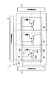
- FIG. 2 is a diagram illustrating an example of a circuit configuration of the display device.
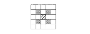
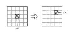
- FIG. 3 is a diagram for explaining the principle of distributing the luminance of a protection target pixel to surrounding pixels.
- FIG. 4 is a diagram illustrating another example of the arrangement of surrounding pixels to which luminance is distributed.
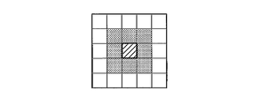
- FIG. 5 is a diagram showing still another example of the arrangement of surrounding pixels to which luminance is distributed.
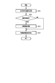
- FIG. 6 is a diagram illustrating an example of a processing procedure of the display device when displaying an image on the display panel.
- FIG. 7 is a diagram illustrating an example of a processing procedure of the first distribution processing.
- FIG. 1 is a perspective view schematically illustrating an example of the configuration of the display device according to the embodiment.
- FIG. 2 is a diagram illustrating an example of a circuit configuration of the display device.
- FIG. 3 is a diagram for explaining the principle of distributing
- FIG. 8 is a diagram illustrating an example of a processing procedure of the second distribution processing.
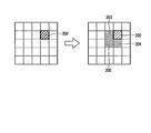
- FIG. 9 is a diagram for specifically explaining the second distribution processing when a pixel is an isolated point.
- FIG. 10 is a diagram for specifically explaining the second distribution processing when a pixel is an isolated point.
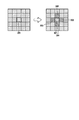
- FIG. 11 is a diagram for specifically explaining the second distribution processing when a pixel is not an isolated point.
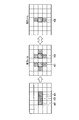
- FIG. 12 is a diagram for describing a case where a plurality of protection target pixels are continuously arranged.
- FIG. 1 is a perspective view schematically showing a configuration of a display device 1 according to the present embodiment.
- FIG. 1 shows a three-dimensional space defined by a first direction X, a second direction Y perpendicular to the first direction X, and a third direction Z perpendicular to the first direction X and the second direction Y.
- first direction X and the second direction Y are orthogonal to each other, they may intersect at an angle other than 90 °.
- the third direction Z is defined as up, and the direction opposite to the third direction Z is defined as down.
- the second member may be in contact with the first member or may be located away from the first member. May be.
- the display device 1 is an organic EL display device (organic EL display) having an organic electroluminescence (EL) element which is a self-luminous element will be mainly described.
- the display device 1 includes a display panel 2, a first circuit board 3, a second circuit board 4, and the like.
- the display panel 2 has a rectangular shape in one example.
- the short side EX of the display panel 2 is parallel to the first direction X
- the long side EY of the display panel 2 is parallel to the second direction Y.
- the third direction Z corresponds to the thickness direction of the display panel 2.
- the main surface of the display panel 2 is parallel to an XY plane defined by a first direction X and a second direction Y.
- the display panel 2 has a display area DA, a non-display area NDA outside the display area DA, and a terminal area MT.
- the non-display area NDA surrounds the display area DA.
- the display area DA is an area for displaying an image, and includes, for example, a plurality of pixels PX arranged in a matrix.
- the pixel PX includes an organic EL element to be described later, a switching element for driving the organic EL element, and the like.
- the terminal area MT is provided along the short side EX of the display panel 2 and includes a terminal for electrically connecting the display panel 2 to an external device or the like.
- the first circuit board 3 is mounted on the terminal area MT and is electrically connected to the display panel 2.
- the first circuit board 3 is, for example, a flexible printed circuit board.
- the first circuit board 3 includes a drive IC chip (hereinafter, referred to as a panel driver) 5 for driving the display panel 2 and the like.
- the panel driver 5 is disposed on the first circuit board 3, but may be disposed below.
- the second circuit board 4 is, for example, a flexible printed circuit board.
- the second circuit board 4 is connected to the first circuit board 3, for example, below the first circuit board 3.
- the panel driver 5 is connected to a control board (not shown) via, for example, the second circuit board 4.
- the panel driver 5 performs control to display an image on the display panel 2 by causing the organic EL elements included in the display panel 2 to emit light based on image data (pixel signals) output from the control board, for example.
- the display panel 2 may have a bent area BA indicated by oblique lines.
- the bending area BA is an area that is bent when the display device 1 is housed in a housing of an electronic device or the like.
- the bending area BA is located on the terminal area MT side in the non-display area NDA. In a state where the bending area BA is bent, the first circuit board 3 and the second circuit board 4 are arranged below the display panel 2 so as to face the display panel 2.
- FIG. 2 shows an example of a circuit configuration of the display device 1 shown in FIG. 2, the display device 1 includes a scanning line driving unit 11, a data signal line driving unit 12, and a power line driving unit 13.
- a plurality of pixels PX are arranged in a matrix in the display area DA.
- FIG. 2 shows only one of the plurality of pixels PX for convenience.
- the pixel PX includes, for example, three sub-pixels (sub-pixels) SR, SG, and SB.
- a plurality of scanning lines WSL extending along the row direction of the plurality of pixels PX arranged in a matrix and a plurality of power supply lines DSL extending in parallel with the plurality of scanning lines WSL are provided.
- a plurality of data signal lines SGL extending along the column direction of the plurality of pixels PX.
- One end of the scanning line WSL is connected to the scanning line driving unit 11.
- One end of the data signal line SGL is connected to the data signal line drive unit 12.
- One end of the power supply line DSL is connected to the power supply line driving unit 13.
- a sub-pixel SR having a light-emitting element emitting red, a sub-pixel SG having a light-emitting element emitting green, and a sub-pixel SB having a light emitting element emitting blue are provided. Are located. The arrangement of these sub-pixels SR, SG and SB can be changed as appropriate.
- the pixel PX may further include, for example, a sub-pixel having a light-emitting element that emits white light in addition to red, green, and blue. Further, the pixel PX may have a configuration including one sub-pixel.
- the sub-pixel SR includes a selection transistor WSTr, a driving transistor DSTr, a capacitor Cs, a light emitting element 21, and the like.
- Light emitting element 21 is an organic EL light emitting element including an organic EL layer disposed between an anode electrode and a cathode electrode.
- the gate electrode of the selection transistor WSTr is connected to the scanning line WSL.
- a source electrode of the selection transistor WSTr is connected to the data signal line SGL.
- a drain electrode of the selection transistor WSTr is connected to a first electrode of the capacitor Cs and a gate electrode of the drive transistor DSTr.
- the source electrode of the drive transistor DSTr is connected to the second electrode of the capacitor Cs and the anode electrode of the light emitting element 21.
- a drain electrode of the driving transistor DSTr is connected to the power supply line DSL.
- the selection transistor WSTr supplies a data signal supplied from the data signal line SGL to the gate electrode of the driving transistor DSTr in synchronization with the selection signal.
- the capacitance element Cs holds the gate potential of the driving transistor DSTr.
- the drive transistor DSTr supplies a drain current based on the gate potential to the light emitting element 21.
- the light emitting element 21 emits light at a luminance corresponding to the drain current.
- sub-pixel SR has been described, but since the other sub-pixels SG and SB have the same configuration, the description of the sub-pixels SG and SB will be omitted.
- the display device 1 can display an image on the display panel 2 (display area DA) by controlling the luminance (light emission) of the light emitting element of each of the plurality of pixels PX.
- the display device 1 organic EL display device
- the plurality of pixels PX having the organic EL elements are arranged as described above
- a specific pixel The load is concentrated on the organic EL element
- a phenomenon called image sticking may occur.
- the pixel on which the load is concentrated is defined as a pixel to be protected (hereinafter, referred to as a pixel to be protected), and the pixel to be protected when displaying an image.
- a pixel to be protected By distributing the luminance to pixels arranged around the pixel to be protected (hereinafter simply referred to as surrounding pixels), the burden on the pixel to be protected is reduced.
- the “luminance of the pixel to be protected” corresponds to the luminance of the light emitting element of the pixel to be protected. Further, “distributing the luminance of the pixel to be protected” refers to decreasing the luminance of the pixel to be protected and increasing the luminance of another pixel in accordance with the decrease in the luminance of the pixel to be protected.
- one block divided into a lattice shape represents one pixel.
- the pixel 101 shown on the left side of FIG. 3 is a protection target pixel.
- the luminance of the pixel 101 is distributed to the surrounding pixels as shown on the right side of FIG.
- the luminance of the pixel 101 is lower than the pixel 102 disposed above the pixel 101, the pixel 103 disposed to the right of the protection target pixel 101, and the lower side of the protection target pixel 101.
- the pixels are distributed to the arranged pixels 104 and the pixels 105 arranged on the left side of the protection target pixel 101.
- the luminance of the pixel 101 can be reduced, so that the burden on the pixel 101 is reduced. can do.
- the light emission of the light emitting element included in the pixel 101 is suppressed, and the suppressed light emission amount is compensated for by the light emitting element included in each of the surrounding pixels 102 to 105, thereby burdening the pixel 101. Can be avoided.
- the luminance of the pixel 101 is distributed to pixels that are arranged at a position where a decrease in image quality (color change) when the luminance of the pixel 101 is distributed is difficult to recognize.
- the luminance of the pixel 101 is distributed to the pixels 102 to 105 arranged (adjacent) in the vertical and horizontal directions of the pixel 101, but the luminance of the pixel 101 is shown in FIG. As described above, it may be distributed to four pixels arranged in the oblique direction of the pixel 101, or may be distributed to eight pixels arranged so as to surround the pixel 101 as shown in FIG.
- the luminance of the pixel 101 may be distributed to a plurality of pixels, or may be distributed to one pixel. Note that, when a large amount of luminance is distributed (distributed) to one pixel, a change in color is easily recognized, and in such a case, the luminance may be distributed to a plurality of pixels. preferable.
- the distribution of luminance in the present embodiment is executed in units of sub-pixels. That is, in the present embodiment, it is assumed that the protection target pixel is one of the three sub-pixels SR, SG, and SB included in the pixel 101, for example.
- the luminance of the pixel to be protected is Are distributed to the sub-pixels SR included in each of the pixels 102 to 105.
- the sub-pixel SB included in the pixel 101 that is, the sub-pixel having a light-emitting element that emits blue light
- the luminance of the pixel to be protected becomes the pixel around the pixel 101. It is distributed to sub-pixels SB included in each of 102 to 105.
- the luminance of all colors red, green, and blue
- a blurred image occurs in the image after the distribution of the luminance. Therefore, for example, when the sub-pixel SG included in the pixel 101 (that is, a sub-pixel having a light emitting element that emits green light) is a protection target pixel, the above-described sub-pixel SR or SB is a protection target pixel. It is assumed that processing different from the above is performed.
- the panel driver 5 acquires image data from the control board as described above (step S1).
- the image data includes a pixel signal that defines the luminance of each of the sub-pixels included in the plurality of pixels PX arranged on the display panel 2.
- the panel driver 5 displays an image by causing each of the sub-pixels included in the plurality of pixels PX to emit light based on a pixel signal included in the image data.
- “to make a sub-pixel emit light” means to make a light-emitting element included in the sub-pixel emit light.
- steps S2 to S5 are executed for each of the sub-pixels included in the plurality of pixels PX arranged on the display panel 2.
- the sub-pixel to be processed in steps S2 to S5 is referred to as a target pixel.
- the panel driver 5 manages the integrated light emission (lighting) time for each sub-pixel included in the plurality of pixels PX arranged on the display panel 2.
- the integrated light emission time is an integrated value of the light emission time of the light emitting element of each sub-pixel. For example, each time an image is displayed on the display panel 2, the integrated lighting time is updated based on the light emission time of each sub-pixel in displaying the image.
- the integrated light emission time may be a value defined from the light emission luminance and the light emission time of the light emitting element of each sub-pixel.
- the panel driver 5 determines whether or not the target pixel is a protection target pixel with reference to the integrated light emission time of the target pixel managed by the panel driver 5 as described above (step S2).
- step S2 for example, when the integrated light emission time is equal to or more than a predetermined value (hereinafter, referred to as a threshold), the target pixel is determined to be a protection target pixel, and when the integrated light emission time is less than the threshold, Is determined that the target pixel is not the protection target pixel.
- a threshold a predetermined value
- the panel driver 5 determines whether the target pixel is the sub-pixel SR or SB, that is, whether the sub-pixel SR or SB is the protection target pixel. It is determined whether or not it is (step S3).
- the panel driver 5 executes a first distribution process (step S4).
- the first distribution process is a process executed to distribute the luminance of the target pixel to surrounding pixels. In the first distribution process, the luminance of each pixel is changed so that the luminance of the target pixel is reduced and the luminance of the pixels around the target pixel is increased.
- the panel driver 5 executes a second distribution process (step S5).
- the second distribution process is a process of changing the luminance of each pixel so as to decrease the luminance of the target pixel and increase the luminance of the pixels around the target pixel. It is a different process.
- step S4 or S5 it is determined whether the processing in steps S2 to S5 has been performed for all the sub-pixels included in the plurality of pixels PX arranged on the display panel 2 (step S5). S6).
- step S6 If it is determined that the processing has not been executed for all the sub-pixels (NO in step S6), the process returns to step S2 and the processing is repeated. In this case, the processing after step S2 is performed with the sub-pixel for which the processing has not been performed as the target pixel.
- the panel driver 5 defines the luminance changed in the first distribution processing in step S4 and the second distribution processing in step S5.
- the image data including the pixel signal to be output is output (step S7).
- the burden on the protection target pixel (that is, the protection target pixel) is displayed. It is possible to reduce the amount of light emitted from the pixels.
- the processing procedure of the above-described first distribution processing (the processing of step S4 shown in FIG. 6) will be described with reference to the flowchart of FIG. Note that the first distribution process is executed when the sub-pixel SR or SB is a protection target pixel as described above.
- the sub-pixel SR is a protection target pixel
- the sub-pixel SR that is the protection target pixel is referred to as a protection target pixel SR for convenience.
- the panel driver 5 determines a pixel to which the luminance of the protection target pixel SR is to be distributed (step S11).
- the pixel determined in step S11 (hereinafter referred to as a distribution destination pixel) is a sub-pixel SR included in each of the pixels PX around the pixel PX including the protection target pixel SR.
- the panel driver 5 includes a plurality of pixels PX arranged to form a predetermined pattern with respect to the pixels PX including the protection target pixels SR as shown in FIGS. 3 to 5, for example.
- the sub-pixel SR included in each is determined as a distribution destination pixel.
- the sub-pixel SR determined as the distribution destination pixel in step S11 is referred to as a distribution destination pixel SR for convenience.
- a distribution destination pixel SR for convenience.
- the luminance of the protection target pixel SR is distributed to the distribution destination pixels SR determined in step S11 described above.
- the amount of luminance distributed from the protection target pixel SR to the distribution destination pixel SR (hereinafter, referred to as the distribution target pixel SR) , A distribution amount) is determined in advance as a distribution coefficient (distribution ratio) for each distribution destination pixel SR.
- the distribution coefficient is a value indicating the ratio of the amount of luminance distributed to the maximum luminance of the protection target pixel SR.
- the distribution coefficient defined for the distribution destination pixel SR is 50%
- the luminance corresponding to 50% of the maximum luminance of the protection target pixel SR among the luminances of the protection target pixel SR is the luminance. It is distributed to the distribution destination pixels SR.
- step S12 the panel driver 5 determines whether at least one of the distribution destination pixels SR determined in step S11 is a protection target pixel (step S12).
- the process in step S12 is the same as the process in step S2 shown in FIG. 6 described above, and thus a detailed description thereof will be omitted.
- the panel driver 5 determines the distribution destination pixel SR determined to be the protection target pixel.
- the distribution coefficient is adjusted (step S13). In step S13, for example, the distribution amount of the luminance to the distribution destination pixel SR determined to be the protection target pixel is reduced, and the distribution amount of the luminance to the distribution destination pixels SR other than the distribution destination pixel SR (the protection target pixel) is reduced.
- the process of adjusting (changing) the distribution coefficient determined for each distribution destination pixel SR is performed so as to increase the distribution coefficient.
- step S13 If it is determined that all of the distribution destination pixels SR are not protection target pixels (NO in step S12), the processing in step S13 is not performed.
- the panel driver 5 generates the protection target pixel SR and the distribution target pixel SR determined in step S11 based on the pixel signal included in the image data acquired in step S1 shown in FIG.
- a signal value (pixel value) of a pixel signal defining each luminance is calculated (step S14).
- the signal value of the pixel signal defining the luminance of each of the protection target pixel SR and the distribution destination pixel SR included in the image data is changed to the pixel value calculated in step S14.
- the image data including the pixel value (pixel signal) calculated in step S14 is output in step S7 shown in FIG.
- the first distribution processing will be specifically described with reference to FIG.
- a description will be given assuming that the pixel PX including the protection target pixel SR is the pixel 101 shown on the left side of FIG.
- the signal value of the pixel signal that defines the luminance of each pixel is referred to as the pixel value of the pixel for convenience.
- the pixel value of the pixel 101 including the protection target pixel SR included in the image data acquired in step S1 shown in FIG. 6 is (255, 255, 255). That is, each pixel value of the sub-pixels SR, SG, and SB included in the pixel 101 is 255 (pixel value defining the maximum luminance), and the pixel 101 is assumed to display white.
- step S11 the pixels are arranged so as to form a predetermined pattern on the pixel 101 including the protection target pixel SR.
- the sub-pixel SR included in each of the pixels is determined as a distribution destination pixel.
- distribution destination pixels SR1 to SR4 the sub-pixels SR included in each of the pixels 102 to 105 determined as the distribution destination pixels.
- step S14 the process of step S14 is performed.
- the pixel values of the protection target pixel SR and the distribution destination pixels SR1 to SR4 are calculated.
- the pixel values of the protection target pixel SR and the distribution destination pixels SR1 to SR4 calculated in step S14 will be specifically described. It is assumed that a distribution coefficient for each of the distribution destination pixels SR1 to SR4 is 25% in advance.
- the pixel value of the protection target pixel SR will be described.
- 25% is determined as the distribution coefficient for each of the distribution destination pixels SR1 to SR4 as described above
- the luminance of the protection target pixel SR is distributed to each of the distribution destination pixels SR1 to SR4 by 25% of the maximum luminance. Is done. Since the luminance of the protection target pixel SR is the maximum luminance (pixel value is 255), the pixel value of the protection target pixel SR after the distribution of the luminance (that is, the pixel value of the sub-pixel SR included in the pixel 101) Is calculated as 0.
- the pixel value of the distribution destination pixel SR1 will be described.
- 25% is determined as the distribution coefficient for the distribution destination pixel SR1 as described above, the luminance corresponding to 25% of the maximum luminance of the luminance of the protection target pixel value SR is distributed to the distribution destination pixel SR1.
- the pixel value that defines the luminance corresponding to 25% of the maximum luminance of the protection target pixel SR is 132. Therefore, 132 is calculated as the pixel value of the distribution destination pixel SR1 after the distribution of the luminance (that is, the pixel value of the sub-pixel SR included in the pixel 102).
- the pixel value of the distribution destination pixel SR1 has been described, but the same applies to the pixel values of the other distribution destination pixels SR2 to SR4. That is, the pixel values of the pixels 103 to 105 after the luminance distribution are (132, 0, 0), similarly to the pixel value of the pixel 102.
- the pixel value of the pixel 101 is changed from (255, 255, 255) to (0, 255, 255),
- the pixel values of the pixels 102 to 105 are changed from (0, 0, 0) to (132, 0, 0).
- the protection target pixel SR (the sub-pixel SR included in the pixel 101) does not need to emit light, so that the burden on the protection target pixel SR is reduced. Can be reduced.
- the luminance to be ensured by the light emission of the protection target pixel SR can be supplemented by the distribution destination pixels SR1 to SR4.
- step S13 shown in FIG. 7 is performed, and the distribution coefficient for the protection target pixel is adjusted.
- the distribution destination pixel SR1 is a protection target pixel.
- step S13 a process of reducing the distribution coefficient for the distribution destination pixel SR1 and increasing the distribution coefficient for the distribution pixels SR2 to SR4 other than the distribution destination pixel 102 is performed. Is executed.
- the distribution coefficient for the distribution destination pixel SR1 is 25% to 10%
- the distribution coefficient for the distribution destination pixels SR2 to SR4 is 25% to 30%, respectively.
- a pixel value that defines a luminance corresponding to 10% of the maximum luminance is calculated.
- the pixel values of the distribution destination pixels SR2 to SR4 after the distribution of the luminance the pixel values defining the luminance corresponding to 30% of the maximum luminance are calculated.
- the burden on the distribution destination pixel SR1 can be reduced by adjusting the distribution coefficient for each of the distribution destination pixels SR1 to SR4. it can.
- the distribution coefficient for the distribution target pixel SR1 as the protection target pixel has been described as being small, but the distribution coefficient for the distribution destination pixel SR1 may be adjusted to be zero.
- the distribution coefficient for the distribution destination pixel SR1 is 25% to 0%
- the distribution coefficient for each of the other distribution destination pixels SR2 to SR4 may be 25% to 33.3% or the like. According to this, it is possible to further reduce the load on the distribution destination pixel SR1 which is the protection target pixel. For example, when the distribution destination pixel SR1 is a protection target pixel, the distribution destination pixel SR1 may be changed to another pixel (sub-pixel SR).
- the display panel 2 when the definition of the display panel 2 is high (that is, the display panel 2 is a high-definition panel), since the pixels are small, the luminance from the protection target pixel SR to the distribution destination pixels SR1 to SR4 is as described above. Even if the distribution amount of is large, it is difficult to visually recognize the change in color.
- the pixels are large as compared with the high-definition panel. Therefore, when the distribution amount of luminance from the protection target pixel SR to the distribution destination pixels SR1 to SR4 is large, the color Changes are easy to see.
- the distribution amount of luminance from the protection target pixel SR1 to the distribution destination pixels SR1 to SR4 may be reduced.
- the distribution coefficient for each of the distribution destination pixels SR1 to SR4 is set to 25% as described above, and when the definition of the display panel 2 is low, the distribution destination pixel SR1 is reduced.
- the distribution coefficient for each of SR1 to SR4 can be, for example, 12.5%.
- the pixel value of the protection target pixel SR before the luminance is distributed is 255 (luminance 100%)
- 50% of the luminance of the protection target pixel SR is distributed to each of the distribution destination pixels SR1 to SR4.
- the pixel value defining the remaining luminance (luminance corresponding to 50% of the maximum luminance) of the protection target pixel SR is 186. Therefore, when the distribution coefficient for each of the distribution destination pixels SR1 to SR4 is 12.5%, 186 is calculated as the pixel value of the protection target pixel SR after the luminance is distributed.
- the pixel value defining the luminance corresponding to 12.5% of the maximum luminance distributed to each of the distribution destination pixels SR1 to SR4 is 65. Therefore, when the distribution coefficient for each of the distribution destination pixels SR1 to SR4 is 12.5%, 65 is calculated as the pixel value of each of the distribution destination pixels SR1 to SR4 after the luminance is distributed.
- the pixel value of the pixel 101 including the protection target pixel SR is (0, 255, 255).
- the pixel values of the pixels 101 to 105 including the distribution destination pixels SR1 to SR4 are respectively (132, 0, 0).
- the pixel value of the pixel 101 is (186, 255, 255), and the pixels 102 to 105 Are (65, 0, 0).
- the protection target pixel SR included in the pixel 101 needs to emit light at the luminance specified by the pixel value “186” (luminance corresponding to 50% of the maximum luminance), the burden on the protection target pixel SR is reduced.
- the reduction ratio decreases, the difference in luminance between the pixels 101 to 105 before and after the luminance is distributed can be reduced by suppressing the luminance distribution amount from the protection target pixel SR to the distribution destination pixels SR1 to SR4. . According to this, even when the definition of the display panel 2 is low, it is possible to make it difficult to visually recognize a change in color due to the distribution of luminance.
- the distribution coefficients (luminance distribution amounts) for the distribution destination pixels SR1 to SR4 may be configured to be different based on the definition of the display panel 2.
- the resolution of the display panel 2 is 350 ppi or more
- the distribution coefficient when the definition of the display panel 2 is high (for example, 25% ) May be adopted, and when the resolution of the display panel 2 is less than 350 ppi, the distribution coefficient (for example, 12.5%) when the definition of the display panel 2 is low may be adopted.
- the level of definition of the display panel 2 may be determined based on another criterion.
- the distribution coefficient may be changed according to the luminance (pixel value) of the protection target pixel SR. Further, even when the distribution coefficient is not changed, the load on the protection target pixel SR may be further reduced by increasing the number of distribution destination pixels according to the luminance of the protection target pixel SR.
- the same distribution coefficient is determined for the distribution destination pixels SR1 to SR4. However, if it is possible to suppress a decrease in image quality due to the distribution of luminance from the protection target pixel SR, the protection is performed. Different distribution coefficients may be determined for the distribution destination pixels SR1 to SR4 according to the positional relationship with respect to the target pixel SR.
- the first distribution processing mainly performed when the sub-pixel SR is the protection target pixel has been described.
- the sub-pixel SB is the protection target pixel
- the sub-pixel SB is determined as the distribution destination pixel. Otherwise, the same processing as described above is performed. For this reason, the detailed description of the first distribution processing executed when the sub-pixel SB is the protection target pixel is omitted.
- the processing procedure of the above-described second distribution processing (the processing of step S5 shown in FIG. 6) will be described with reference to the flowchart of FIG. Note that the second distribution process is executed when the sub-pixel SG is a protection target pixel as described above.
- the sub-pixel SG that is the pixel to be protected is referred to as a pixel to be protected SG for convenience.
- the panel driver 5 determines whether or not the pixel PX including the protection target pixel SG is an isolated point based on the image data obtained in step S1 shown in FIG. 6 (step S21).
- the pixel PX is an isolated point means that the color displayed by the pixel PX is different from the color displayed by the surrounding pixels PX (another pixel PX adjacent to the pixel PX). It means that. That is, as described with reference to FIG. 3 described above, for example, the pixel value of the pixel 101 is (255, 255, 255), and the pixel value of the pixel PX around the pixel 101 is (0, 0, 0). In such a case, the pixel 101 is determined to be an isolated point.
- the color displayed by each pixel PX can be determined based on a pixel signal (pixel value) included in the image data.
- the luminance of the protection target pixel SG that is, green
- a blurred feeling occurs in the image after the luminance distribution. Therefore, in the present embodiment, when the pixel PX including the protection target pixel SG is an isolated point, the luminance of the pixel PX including the protection target pixel SG moves (shifts) to the surrounding pixels PX (adjacent pixels PX). )It shall be.
- the panel driver 5 is a destination of the luminance of the pixel PX including the protection target pixel SG.
- the pixel is determined (Step S22).
- the pixel determined in step S22 (hereinafter, referred to as a destination pixel) is, for example, one of the pixels PX around the pixel PX including the protection target pixel SG.
- the process of determining the destination pixel in step S22 will be specifically described.
- the destination pixel is determined as follows.
- a pixel PX similar in color to the pixel PX is determined as a destination pixel. I do.
- the pixel PX similar in color to the pixel PX including the protection target pixel SG can be determined based on a pixel signal (pixel value of each sub-pixel included in the pixel PX) included in the image data.
- the image displayed based on the image data is a moving image
- the motion vector direction of a moving image can be obtained, for example, from image data.
- the pixel PX located in the movement direction from the pixel PX. Is determined as the destination pixel.
- a head mounted display HMD
- VR Virtual Reality
- the typical movement can be obtained from various sensors (for example, an acceleration sensor or a gyro sensor) mounted on the electronic device.
- the pixel PX determined as the destination pixel in step S22 is referred to as a destination pixel PX for convenience.
- Step S23 the panel driver 5 determines whether or not the sub-pixel SR, SG or SB included in the destination pixel PX determined in Step S22 is a protection target pixel.
- the process in step S23 is the same as the process in step S2 shown in FIG. 6 described above, and a detailed description thereof will be omitted here.
- the panel driver 5 changes the destination pixel PX determined in step S22. (Step S24). In this case, a new destination pixel PX is determined from the pixels PX other than the destination pixel PX determined in step S22 among the pixels PX around the pixel PX including the protection target pixel SG.
- step S24 If the sub-pixels SR, SG, and SB included in the destination pixel PX are determined not to be the protection target pixels (NO in step S23), the process in step S24 is not performed.
- the destination pixel PX is the destination pixel PX determined in step S22 when the process of step S24 is not performed, and is the same as the destination pixel PX when the process of step S24 is performed. It is assumed that the new destination pixel PX has been changed in S24.
- the panel driver 5 calculates the pixel values of the sub-pixels SR, SG, and SB included in the destination pixel PX based on the pixel signals included in the image data acquired in step S1 illustrated in FIG. Step S25).
- the pixel values of the sub-pixels SR, SG, and SB included in the destination pixel PX calculated in step S25 are such that the luminance of the pixel PX including the protection target pixel SG is the luminance of the destination pixel PX before the luminance is moved. This corresponds to a pixel value that defines the added luminance.
- the pixel value of the destination pixel PX included in the image data is changed to the pixel value calculated in step S25.
- the luminance of the pixel PX including the protection target pixel SG is moved to the destination pixel PX, the sub-pixels SR and SG included in the destination pixel PX (that is, the pixels other than the sub-pixel SG)
- the source direction refers to the direction from the destination pixel PX to the pixel PX including the protection target pixel SG (that is, the source pixel PX).
- the panel driver 5 determines a pixel to which the luminance of the sub-pixels SR and SB included in the destination pixel PX is to be distributed, based on the above-mentioned source direction (step S26).
- the pixels determined in step S25 include sub-pixels SR and SB included in each of the pixels PX located in the source direction from the destination pixel PX.
- distribution destination pixels SR and SB the sub-pixels SR and SB determined as the distribution destination pixels in step S25 are referred to as distribution destination pixels SR and SB, respectively.
- the description will be made assuming that there are a plurality of distribution destination pixels SR and SB, respectively, but it may be one.
- the sub-pixels SR and SB included in the destination pixel PX are referred to as distribution source pixels SR and SB, respectively.
- the distribution amount of the luminance from the distribution source pixel SR to the distribution destination pixel SR is determined in advance as a distribution coefficient for each distribution destination pixel SR.
- the distribution amount of the luminance from the distribution source pixel SB to the distribution destination pixel SB is predetermined for each distribution destination pixel SB as a distribution coefficient.
- step S27 the panel driver 5 determines whether or not the distribution destination pixel SR or SB determined in step S26 is a protection target pixel (step S27).
- the process in step S27 is the same as the process in step S2 shown in FIG. 6, and a detailed description thereof is omitted here.
- the panel driver 5 determines the distribution destination pixel SR or SB determined to be the protection target pixel.
- the distribution coefficient is adjusted (step S28).
- step S28 when it is determined that at least one of the distribution target pixels SR is a protection target pixel, in step S28, the distribution of luminance to the distribution destination pixel SR determined to be the protection target pixel SR is performed.
- the distribution coefficient determined for each distribution destination pixel SR is adjusted (changed) so as to reduce the amount and increase the distribution amount of luminance to the distribution destination pixels SR other than the distribution destination pixel SR (protection target pixel). ) Is performed.
- step S28 when it is determined that at least one of the distribution destination pixels SB is a protection target pixel, in step S28, the luminance distribution amount to the distribution destination pixel SB determined to be the protection target pixel is determined.
- the distribution coefficient determined for each distribution pixel SB is adjusted (changed) so as to reduce the luminance and increase the amount of distribution of luminance to the distribution pixels SB other than the distribution pixel SB (protection target pixel).
- the processing is executed.
- step S28 If it is determined that the distribution destination pixels SR and SB are not protection target pixels (NO in step S27), the processing in step S28 is not performed.
- the panel driver 5 determines the distribution source pixel SR, the distribution destination pixel SR, the distribution source pixel SB and the distribution source pixel SR based on the pixel signal included in the image data acquired in step S1 shown in FIG.
- the pixel value of each of the preceding pixels SB is calculated (step S29).
- the pixel values of the distribution source pixel SR, the distribution destination pixel SR, the distribution source pixel SB, and the distribution destination pixel SB included in the image data are changed to the pixel values calculated in step S29.
- the image data including the pixel value (image signal) calculated in step S29 is output in step S7 shown in FIG.
- step S21 if it is determined in step S21 that the pixel PX including the protection target pixel SG is not an isolated point (NO in step S21), step S26 is performed. It is assumed that the following processing is executed.
- the pixel PX is not an isolated point means that, for example, the color displayed by the pixel PX is the same as the color displayed by the pixels PX around the pixel PX.
- the image displayed based on the image data is, for example, a solid image (screen) in which the same color is displayed in all of the plurality of pixels PX, the pixel PX including the protection target pixel SG Is determined not to be an isolated point.
- step S26 executed in this case is the same as the processing of steps S11 to S14 shown in FIG. That is, when the pixel PX including the protection target pixel SG is not an isolated point, the luminance of the protection target pixel SG is distributed to the sub-pixels SG included in each of the pixels PX around the pixel PX including the protection target pixel SG. You.
- the second distribution processing will be specifically described.
- the case where the pixel PX including the protection target pixel SG is an isolated point and the case where the pixel PX including the protection target pixel SG is not an isolated point will be described separately.
- the pixel value of the pixel 201 including the protection target pixel SG included in the image data acquired in step S1 shown in FIG. 6 is (255, 255, 255). That is, each pixel value of the sub-pixels SR, SG, and SB included in the pixel 201 is 255, and the pixel 201 is assumed to display white.
- the pixel values of a plurality of pixels PX other than the pixel 201 included in the image data acquired in step S1 shown in FIG. 6 are (0, 0, 0). That is, the pixel values of the sub-pixels SR, SG, and SSB included in the pixels PX other than the pixel 201 are each 0, and the plurality of pixels PX display black.
- the pixel 201 including the protection target pixel SG has a different color from the pixel PX around the pixel 201. Therefore, in step S21 shown in FIG. 8, the pixel 201 is determined to be an isolated point.
- a pixel to which the luminance of the pixel 201 is to be moved (a destination pixel) is determined.
- the pixel 202 shown on the right side of FIG. 9 is determined as a destination pixel (hereinafter, referred to as a destination pixel 202).
- the destination pixel 202 is a pixel PX located on the upper right of the pixel 201 including the protection target pixel SG. Note that the details of the determination processing of the destination pixel are the same as those described with reference to FIG. 8, and a detailed description thereof will be omitted here.
- the luminance of the pixel 201 including the protection target pixel SG is moved to the destination pixel 202.
- the pixel value of the pixel 201 is changed from (255, 255, 255) to (0, 0, 0).
- the sub-pixels SR, SG, and SB included in the destination pixel 202 are not protection target pixels. However, if the sub-pixel SR, SG, or SB is a protection target pixel, the destination pixel 202 Is changed to another pixel PX other than the pixel 202.
- the sub-pixel SR, SG, or SB included in the destination pixel 202 is a pixel to be protected, for example, not all of the luminance is moved to the sub-pixel that is the pixel to be protected; May be moved, or the luminance may be distributed to a plurality of pixels including the sub-pixel (that is, the distribution coefficient may be adjusted).
- the sub-pixels SR and SB included in the destination pixel 202 are Are distributed in the source direction.
- step S26 shown in FIG. 8 the pixel PX located in the movement source direction of the movement destination pixel 202 is specified.
- the source direction of the destination pixel 202 is a direction on the pixel 201 side including the protection target pixel SG when viewed from the destination pixel 202.
- the pixels PX arranged to form a predetermined pattern from the destination pixel 202 toward the source direction are specified.
- the pixels 203 to 205 shown on the right side of FIG. 10 have been specified. According to this, the sub-pixels SR and SB included in each of the pixels 203 to 205 are determined as the distribution destination pixels.
- the sub-pixels SR included in each of the pixels 203 to 205 determined as the distribution destination pixels are referred to as distribution destination pixels SR11 to SR13, and the sub-pixel SB included in each of the pixels 203 to 205 is referred to as a sub-pixel SB.
- the pixels are referred to as distribution destination pixels SB11 to SB13.
- the sub-pixels SR and SB included in the destination pixel 202 are referred to as distribution source pixels SR and SB, respectively.
- step S29 If all of the distribution destination pixels SR11 to SR13 and the distribution destination pixels SB11 to SB13 are not the protection target pixels, the process of step S29 is executed.
- step S29 the pixel values of the distribution source pixel SR, the distribution destination pixels SR11 to SR13, the distribution source pixel SB, and the distribution destination pixels SB11 to SB13 are calculated.
- step S29 the pixel values of the distribution source pixel SR and the distribution destination pixels SR11 to SR13 calculated in step S29 will be specifically described.
- the pixel value of the destination pixel 202 is (255, 255, 255). That is, the pixel value of the distribution source pixel SR (that is, the sub-pixel SR included in the movement destination pixel 202) is 255.
- the luminance (maximum luminance) of the distribution source pixel SR when the luminance corresponding to 50% of the maximum luminance is distributed to the distribution destination pixels SR11 to SR13, the remaining luminance of the distribution source pixel SR (maximum luminance) is 186. Therefore, 186 is calculated as the pixel value of the distribution source pixel SR after the luminance distribution.
- the pixel value defining the luminance corresponding to 16.7% of the maximum luminance distributed to the distribution destination pixels SR11 to SR13 is 112.
- 112 is calculated as the pixel value of the distribution destination pixels SR11 to SR13 after the luminance is distributed.
- the pixel values of the distribution source pixel SR and the distribution destination pixels SR11 to SR13 have been described, but the same applies to the pixel values of the distribution source pixel SB and the distribution destination pixels SB11 to SB13.
- the pixel value that defines the luminance corresponding to% is 186. Therefore, 186 is calculated as the pixel value of the distribution source pixel SB after the luminance is distributed.
- the pixel value that defines the luminance corresponding to 16.7% of the maximum luminance distributed to the distribution destination pixels SB11 to SB13 is 112. For this reason, 112 is calculated as the pixel value of the distribution destination pixels SB11 to SB13 after the luminance is distributed.
- the pixel value of the pixel 201 is (0, 0, 0).
- the pixel values of the other pixels 203 to 205 are (0, 0, 0).
- step S29 when the above-described processing of step S29 is performed, the pixel value of the movement destination pixel 202 is changed from (255, 255, 255) to (186, 255, 186), and the pixels 203 to 205 The values are changed from (0,0,0) to (112,0,112), respectively.
- the light-emitting element of the protection target pixel SG included in the pixel 201 When an image is displayed based on the image data including such a pixel value, it is not necessary to cause the light-emitting element of the protection target pixel SG included in the pixel 201 to emit light, so that the burden on the protection target pixel SG is reduced. Can be reduced. Further, the luminance to be ensured by the light emission of the protection target pixel SG can be supplemented by the sub-pixel SG included in the destination pixel 202. Further, the luminance of the pixel 201 is distributed to the sub-pixel SR and the sub-pixel SB included in each of the pixels 203 to 205 by distributing the luminance of the sub-pixel SR and the sub-pixel SB included in the destination pixel 202. , The influence of the movement of the center of gravity can be reduced.
- distribution coefficients may be determined for the distribution destination pixels SR11 to SR13 and the distribution destination pixels SB11 to SB13. Further, different distribution coefficients may be determined for each of the distribution destination pixels SR11 to SR13 according to the positional relationship with respect to the movement destination pixel 202. Similarly, different distribution coefficients may be determined for each of the distribution destination pixels SB11 to SB13 according to the positional relationship with respect to the movement destination pixel 202.
- the pixel PX including the protection target pixel SG is not an isolated point
- the luminance of the protection target pixel SG is distributed to pixels (sub-pixels SG) around the protection target pixel SG.
- the description will be made on the assumption that the pixel PX including the protection target pixel SG is the pixel 301 shown on the left side of FIG.
- the pixel value of the pixel 301 including the protection target pixel SG included in the image data acquired in step S1 shown in FIG. 6 is (128, 128, 128). That is, each pixel value of the sub-pixels SR, SG, and SB included in the pixel 301 is 128, and the pixel 301 is assumed to display gray.
- each pixel value of the sub-pixels SR, SG, and SB included in the plurality of pixels PX other than the pixel 301 is 128, and the plurality of pixels PX display gray similarly to the pixel 301. I do.
- the image displayed based on the image data acquired in step S1 shown in FIG. 6 is a solid image in which all pixels PX display gray.
- the pixel 301 including the protection target pixel SG has the same color as the pixel PX around the pixel 301. Therefore, in step S21 shown in FIG. 8, it is determined that the pixel 301 is not an isolated point.
- step S26 the sub-pixel SG included in each of the pixels arranged to form a predetermined pattern with respect to the pixel 301 including the protection target pixel SG is determined as the distribution destination pixel.
- the sub-pixel SG included in each of the pixels 302 to 305 shown on the right side of FIG. 11 has been determined as a distribution destination pixel.
- the sub-pixel SG included in each of the pixels 302 to 305 arranged so as to form a pattern similar to the case where the above-described sub-pixel SR is the pixel to be protected is determined as the distribution destination pixel.
- the distribution destination pixel may be determined in a different pattern for each of the sub-pixels SR, SB, and SB.
- the sub-pixels SG included in each of the pixels 302 to 305 determined as the distribution destination pixels are referred to as distribution destination pixels SG1 to SG4.
- step S29 if all of the distribution destination pixels SG1 to SG4 are not protection target pixels, the process of step S29 is executed.
- the pixel values of the protection target pixel SG and the distribution destination pixels SG1 to SG4 are calculated.
- the pixel values of the protection target pixel SG and the distribution destination pixels SG1 to SG4 calculated in step S29 will be specifically described. It is assumed that a distribution coefficient for each of the distribution destination pixels SG1 to SG4 is 2.5% in advance.
- the pixel value of the protection target pixel SG will be described.
- the luminance of the protection target pixel SG is set to the maximum luminance of 2. Dispensed in 5% increments.
- the pixel value of the protection target pixel SG is 128, and the luminance of the protection target pixel SG corresponds to 21.5% of the maximum luminance. That is, among the luminances of the protection target pixel SG, luminance equivalent to 10% of the maximum luminance in total is distributed to the distribution destination pixels SG1 to SG4. Therefore, the luminance of the protection target pixel SR after the luminance distribution is maximized.
- the brightness is equivalent to 11.5% of the brightness.
- 96 is calculated as the pixel value of the protection target pixel SG after the distribution of the luminance (that is, the pixel value of the sub-pixel SG included in the pixel 301).
- the pixel value of the distribution destination pixel SG1 will be described.
- 2.5% is determined as the distribution coefficient for the distribution destination pixel SG1 as described above, of the luminance of the protection target pixel SG, a luminance corresponding to 2.5% of the maximum luminance is distributed to the distribution destination pixel SG1. Is done.
- the pixel value of the distribution destination pixel SG1 before the luminance is distributed is 128, but the luminance defined by the pixel value corresponds to 21.5% of the maximum luminance as described above. For this reason, when the luminance equivalent to 2.5% of the maximum luminance is distributed to the distribution destination pixel SG1 from the protection target pixel SG, the luminance of the distribution destination pixel SG1 after the luminance distribution is 24% of the maximum luminance. (21.5% + 2.5%).
- the pixel value that defines the luminance corresponding to 24% of the maximum luminance is 133. Therefore, 133 is calculated as the pixel value of the distribution destination pixel SG1 after the distribution of the luminance (that is, the pixel value of the sub-pixel SG included in the pixel 302).
- the pixel value of the distribution destination pixel SG1 has been described, but the same applies to the pixel values of the other distribution destination pixels SG2 to SG4. That is, the pixel values of the pixels 303 to 305 after the distribution of the luminance are (128, 133, 128) as in the case of the pixel 302.
- the pixel value of the pixel 301 is (128, 128, 128) to (128, 96, 128).
- the pixel values of the pixels 302 to 305 are changed from (128, 128, 128) to (128, 133, 128).
- the protection target pixel SG is compared with the case where the image is displayed based on the image data acquired in step S1 shown in FIG. Since the light emission amount of the (sub-pixel SG included in the pixel 301) can be suppressed, the load on the protection target pixel SG can be reduced. Further, the luminance to be secured by the light emission of the protection target pixel SG can be supplemented by the distribution destination pixels SG1 to SG4.
- the same distribution coefficient has been described for each of the distribution destination pixels SG1 to SG4. However, it is possible to suppress deterioration in image quality due to distribution of luminance from the protection target pixel SG. If so, different distribution coefficients may be determined for the distribution destination pixels SG1 to SG4 according to the positional relationship with respect to the protection target pixel SG.
- the luminance of the protection target pixel (first pixel) of the plurality of pixels PX is reduced, and the distribution destination pixel (second pixel) disposed around the protection target pixel is reduced.
- the image is displayed by increasing the luminance of. That is, in the present embodiment, by distributing the luminance of the pixel to be protected to the surrounding pixels, it is possible to prevent the load from being concentrated on a specific pixel (light emitting element) and extend the life of the light emitting element. It becomes possible.
- the luminance of the sub-pixel SR is reduced, and the luminance of the sub-pixel SR included in the pixel PX around the pixel to be protected is increased. Let it. That is, in the present embodiment, it is possible to extend the life of the light emitting element for each subpixel.
- the luminance of the pixel PX including the sub-pixel SG is reduced, and the luminance of the destination pixel PX (second pixel) is reduced.
- the luminance of the sub-pixels SR and SB first and third sub-pixels included in the destination pixel PX is reduced, and the pixel PX (second pixel) arranged around the destination pixel PX is reduced.
- the luminance of the included sub-pixels SR and SB is increased.
- the luminance of the pixel PX including the sub-pixel SG which is the protection target pixel is moved to the destination pixel PX, and the luminance of the sub-pixels SR and SB included in the destination pixel PX is distributed. Accordingly, it is possible to avoid the occurrence of a blurred feeling by simply distributing all colors, and to suppress a decrease in image quality.
- the destination pixel PX is determined based on the motion vector of the moving image. Further, the destination pixel PX may be determined based on the moving direction of the device on which the display device 1 is mounted. In the present embodiment, with such a configuration, the influence of moving or distributing the luminance of each pixel can be made less visible.
- the brightness of the sub-pixels SR and SB included in the destination pixel PX is determined in the direction of the source of the destination pixel PX (that is, in the direction of the pixel PX including the sub-pixel SG that is the protection target pixel). It is distributed to the sub-pixels SR and SB included in the arranged pixels PX.
- by distributing (dispersing) the luminance in the source direction in this way the influence of the movement of the center of gravity when the luminance of the pixel PX including the sub-pixel SG which is the protection target pixel is moved is reduced. It becomes possible.
- the luminance of the pixel PX including the sub-pixel SG which is the protection target pixel is moved to the destination pixel PX when the image displayed based on the image data is a solid image
- the influence of the movement of the luminance is large, and a change in color is easily recognized.
- the pixel PX including the sub-pixel SG, which is the pixel to be protected is an isolated point (that is, the color of the pixel PX is different from the surrounding pixels), the luminance of the pixel PX is changed to the destination pixel PX. , It is possible to make the change in color less visible.
- the amount by which the luminance of the pixel to be protected is reduced according to the definition of the display panel 2 may be different.
- the definition of the display panel 2 when the definition of the display panel 2 is high, priority is given to reducing the load on the pixel to be protected, and when the definition of the display panel 2 is low, the distribution amount of luminance is reduced. Thus, it is possible to make the change in color less visible.
- the distribution destination pixel when the pixel to which the luminance is to be distributed (the distribution destination pixel) is the pixel to be protected, the distribution amount of the luminance to the pixel to be protected may be reduced, or the distribution destination may be reduced.
- the pixel may be changed to another pixel. According to such a configuration, it is possible to suppress an increase in the load on the distribution destination pixels.
- the case where the luminance of one protection target pixel is distributed has been mainly described.
- a plurality of pixels PX arranged consecutively each include a protection target pixel, that is, a plurality of continuous pixels.
- a protection target pixel exists in each of the pixels PX to be protected.
- a plurality of pixels 401 to 403 each including the pixel to be protected are continuously present.
- the luminance of the protection target pixel included in the pixels 401 and 403 is distributed, and when displaying the second frame (image) subsequent to the first frame, A configuration in which the luminance of the protection target pixel included in the pixel 402 is distributed can be employed.
- the display device 1 is described as an organic EL display device having an organic EL element as a light emitting element.
- a large number of LEDs Light Emitting Diode
- It may be applied to an outdoor display device or the like to be used.
- a display panel in which a plurality of pixels having light-emitting elements are arranged, A display control unit that displays an image on the display panel by causing each of the plurality of pixels to emit light based on a pixel signal that defines the luminance of each of the plurality of pixels; With The display control unit decreases the luminance of a first pixel that is a pixel to be protected among the plurality of pixels, and increases the luminance of a second pixel disposed around the first pixel. Display the image Display device.
- Each of the plurality of pixels includes first to third sub-pixels having light-emitting elements having different emission colors,
- the display control unit reduces the luminance of the first sub-pixel and sets the first sub-pixel included in the second pixel. Increase pixel brightness
- the display device according to [C1].
- the luminance of the first and third sub-pixels included in the second pixel is reduced, and the luminance of the first and third sub-pixels included in the third pixel disposed around the second pixel is increased.
- the display control unit may include a color similar to a color displayed on the first pixel among a plurality of pixels arranged around the first pixel.
- the display control unit may select the second pixel from among a plurality of pixels arranged around the first pixel based on a motion vector of the moving image.
- the display device wherein the pixel is determined.
- the display control unit determines the second pixel from among a plurality of pixels arranged around the first pixel based on a moving direction of a device on which the display device is mounted.
- the third pixel is arranged in a direction of the first pixel with respect to the second pixel.
- a color displayed by the first pixel is different from a color displayed by pixels arranged around the first pixel.
- a display method comprising: [C14] Each of the plurality of pixels includes first to third sub-pixels having light-emitting elements having different emission colors, In the displaying, if the pixel to be protected is the first sub-pixel included in the first pixel, the luminance of the first sub-pixel is reduced, and the first sub-pixel included in the second pixel is reduced. Increase pixel brightness
- the displaying step includes: When the sub-pixel to be protected is the second sub-pixel included in the first pixel, the luminance of the first pixel is reduced and the luminance of the second pixel is increased.
- the luminance of the first and third sub-pixels included in the second pixel is reduced, and the luminance of the first and third sub-pixels included in the third pixel disposed around the second pixel is increased.
- the displaying includes a color similar to a color displayed in the first pixel among a plurality of pixels arranged around the first pixel.
- the displaying includes selecting the second pixel from among a plurality of pixels arranged around the first pixel based on a motion vector of the moving image.
- the display method according to [C15] including a step of determining a pixel.
- the displaying step includes a step of determining the second pixel from among a plurality of pixels arranged around the first pixel based on a moving direction of a device on which the display device is mounted [C15].
- Display method. [C19] The display method according to [C15], wherein the third pixel is arranged in a direction of the first pixel with respect to the second pixel.
- [C20] The display method according to [C15], wherein the color displayed by the first pixel is different from the color displayed by pixels arranged around the first pixel.
- [C21] The display method according to [C13], wherein the amount by which the luminance of the first pixel is reduced differs depending on the definition of the display panel.
- [C22] The display method according to [C13], wherein in the displaying step, when the second pixel is a pixel to be protected, an amount of increasing the luminance of the second pixel is reduced.
- the displaying includes changing the second pixel when the second pixel is a pixel to be protected.
- SYMBOLS 1 ... Display apparatus, 2 ... Display panel, 3 ... First circuit board, 4 ... Second circuit board, 5 ... Panel driver (display control part), 21 ... Light emitting element, PX ... Pixel, SR ... Sub-pixel (1st Sub-pixel), SG: sub-pixel (second sub-pixel), SB: sub-pixel (third sub-pixel).
Landscapes
- Engineering & Computer Science (AREA)
- Physics & Mathematics (AREA)
- Computer Hardware Design (AREA)
- General Physics & Mathematics (AREA)
- Theoretical Computer Science (AREA)
- Electroluminescent Light Sources (AREA)
- Control Of Indicators Other Than Cathode Ray Tubes (AREA)
- Control Of El Displays (AREA)
Abstract
実施形態によれば、発光素子を有する複数の画素が配置された表示パネルと、複数の画素の各々の輝度を規定する画素信号に基づいて複数の画素の各々を発光させることによって表示パネルに画像を表示する表示制御部とを具備する表示装置が提供される。表示制御部は、複数の画素のうちの保護の対象となる画素である第1画素の輝度を低下させ、当該第1画素の周辺に配置されている第2画素の輝度を増加させて画像を表示する。
Description
本発明の実施形態は、表示装置に関する。
近年では、例えばスマートフォン等の電子機器に、有機エレクトロルミネッセンス(EL:Electro Luminescence)素子を有する表示装置(以下、有機ELディスプレイと表記)が採用されている。
有機ELディスプレイを採用した場合には、例えば液晶ディスプレイと比較して、電子機器の薄型化及び軽量化を実現することができるとともに、消費電力を低減することができる点で利点がある。
ここで、有機ELディスプレイには複数の画素が配置されており、当該画素の各々が有する発光素子(有機EL素子)が自ら発光することによって、当該ディスプレイに画像が表示される。このため、例えば同一の画像が長時間表示されるような場合には、継続的に高輝度で発光する特定の画素(発光素子)に負担が集中することがある。
このように特定の画素に負担が集中した場合、当該画素の劣化が他の画素よりも進行し、焼付きと称される現象が発生することが知られている。
これに対して、例えば有機ELディスプレイに表示される画像(画面)全体をずらすことによって、特定の画素に負担が集中することを避けるような対策が行われる場合がある。
しかしながら、このような対策では、画像を視認するユーザに違和感(不快感)を与える場合があるし、例えば色彩が均一な画像を表示するような場合には効果を得ることができない。
そこで、本発明の目的は、特定の画素に負担が集中することを避けることが可能な表示装置を提供することにある。
実施形態によれば、発光素子を有する複数の画素が配置された表示パネルと、前記複数の画素の各々の輝度を規定する画素信号に基づいて前記複数の画素の各々を発光させることによって前記表示パネルに画像を表示する表示制御部とを具備する表示装置が提供される。前記表示制御部は、前記複数の画素のうちの保護の対象となる画素である第1画素の輝度を低下させ、当該第1画素の周辺に配置されている第2画素の輝度を増加させて前記画像を表示する。
以下、図面を参照して、実施形態について説明する。なお、開示はあくまで一例に過ぎず、当業者において、発明の趣旨を保っての適宜変更について容易に想到し得るものについては、当然に本発明の範囲に含有されるものである。また、図面は、説明をより明確にするため、実際の態様に比べて、各部の幅、厚さ、形状等について模式的に表される場合があるが、あくまで一例であって、本発明の解釈を限定するものではない。また、本明細書と各図において、既出の図に関して前述したものと同一または類似した機能を発揮する構成要素には同一の参照符号を付し、重複する詳細な説明を適宜省略することがある。
図1は、本実施形態に係る表示装置1の構成を概略的に示す斜視図である。図1は、第1方向Xと、第1方向Xに垂直な第2方向Yと、第1方向X及び第2方向Yに垂直な第3方向Zによって規定される三次元空間を示している。なお、第1方向X及び第2方向Yは、互いに直交しているが、90°以外の角度で交差していてもよい。また、本実施形態において、第3方向Zを上と定義し、第3方向Zと反対側の方向を下と定義する。「第1部材の上の第2部材」及び「第1部材の下の第2部材」とした場合、第2部材は、第1部材に接していてもよく、第1部材から離れて位置していてもよい。
以下、本実施形態においては、表示装置1が自発光素子である有機エレクトロルミネッセンス(EL)素子を有する有機EL表示装置(有機ELディスプレイ)である場合について主に説明する。
図1に示すように、表示装置1は、表示パネル2、第1回路基板3及び第2回路基板4等を備える。
表示パネル2は、一例では矩形状である。図示した例では、表示パネル2の短辺EXは、第1方向Xと平行であり、表示パネル2の長辺EYは、第2方向Yと平行である。第3方向Zは、表示パネル2の厚さ方向に相当する。表示パネル2の主面は、第1方向Xと第2方向Yとにより規定されるX-Y平面に平行である。表示パネル2は、表示領域DA、表示領域DAの外側の非表示領域NDA、及び端子領域MTを有している。図示した例では、非表示領域NDAは、表示領域DAを囲んでいる。
表示領域DAは、画像を表示する領域であり、例えばマトリクス状に配置された複数の画素PXを備えている。画素PXは、後述する有機EL素子と、有機EL素子を駆動するためのスイッチング素子等を含む。
端子領域MTは、表示パネル2の短辺EXに沿って設けられ、表示パネル2を外部装置等と電気的に接続するための端子を含んでいる。
第1回路基板3は、端子領域MTの上に実装され、表示パネル2と電気的に接続されている。第1回路基板3は、例えばフレキシブルプリント回路基板である。第1回路基板3は、表示パネル2を駆動する駆動ICチップ(以下、パネルドライバと表記)5等を備えている。なお、図示した例では、パネルドライバ5は、第1回路基板3の上に配置されているが、下に配置されていてもよい。第2回路基板4は、例えばフレキシブルプリント回路基板である。第2回路基板4は、第1回路基板3の例えば下方において第1回路基板3と接続されている。
ここで、パネルドライバ5は、例えば第2回路基板4を介して制御基板(図示せず)と接続されている。パネルドライバ5は、例えば制御基板から出力される画像データ(画素信号)に基づいて表示パネル2が有する有機EL素子を発光させることによって表示パネル2に画像を表示する制御を実行する。
なお、表示パネル2は、斜線を付して示す折り曲げ領域BAを有していてもよい。折り曲げ領域BAは、表示装置1が電子機器等の筐体に収容される際に折り曲げられる領域である。折り曲げ領域BAは、非表示領域NDAのうち端子領域MT側に位置している。折り曲げ領域BAが折り曲げられた状態において、第1回路基板3及び第2回路基板4は、表示パネル2と対向するように、表示パネル2の下方に配置される。
図2は、図1に示す表示装置1の回路構成の一例を示す。図2において、表示装置1は、走査線駆動部11、データ信号線駆動部12及び電源線駆動部13を備える。
ここで、表示領域DAには、複数の画素PXがマトリクス状に配置されている。図2においては、便宜的に、複数の画素PXのうちの1つのみを示している。画素PXは、例えば3つの副画素(サブピクセル)SR、SG及びSBを含む。また、表示領域DAには、マトリクス状に配置された複数の画素PXの行方向に沿って延伸する複数の走査線WSLと、当該複数の走査線WSLと平行して延伸する複数の電源線DSLと、当該複数の画素PXの列方向に沿って延伸する複数のデータ信号線SGLとが更に配置されている。走査線WSLの一端は、走査線駆動部11に接続される。データ信号線SGLの一端は、データ信号線駆動部12に接続される。電源線DSLの一端は、電源線駆動部13に接続される。
走査線WSLとデータ信号線SGLの交点には、例えば赤色で発光する発光素子を有する副画素SR、緑色で発光する発光素子を有する副画素SG及び青色で発光する発光素子を有する副画素SBが配置されている。これら副画素SR、SG及びSBの配置は適宜変更することができる。画素PXには、例えば赤色、緑色及び青色に加えて、白色を発光する発光素子を有する副画素が更に含まれていてもよい。また、画素PXは、1つの副画素を含む構成であってもよい。
ここで、副画素SRの構成について説明する。副画素SRは、選択トランジスタWSTr、駆動トランジスタDSTr、容量素子Cs及び発光素子21等を有する。
発光素子21は、アノード電極とカソード電極との間に配置された有機EL層を備える有機EL発光素子である。
選択トランジスタWSTrのゲート電極は、走査線WSLに接続されている。選択トランジスタWSTrの例えばソース電極は、データ信号線SGLに接続されている。選択トランジスタWSTrの例えばドレイン電極は、容量素子Csの第1の電極及び駆動トランジスタDSTrのゲート電極に接続されている。
駆動トランジスタDSTrの例えばソース電極は、容量素子Csの第2の電極及び発光素子21のアノード電極に接続されている。駆動トランジスタDSTrの例えばドレイン電極は、電源線DSLに接続されている。
選択トランジスタWSTrは、走査線WSLに選択信号が供給された場合に、選択信号と同期してデータ信号線SGLから供給されるデータ信号を、駆動トランジスタDSTrのゲート電極に供給する。容量素子Csは、駆動トランジスタDSTrのゲート電位を保持する。駆動トランジスタDSTrは、ゲート電位に基づくドレイン電流を発光素子21に供給する。発光素子21は、ドレイン電流に対応した輝度で発光する。
ここでは、副画素SRについて説明したが、他の副画素SG及びSBについても同様の構成であるため、当該副画素SG及びSBについての説明は省略する。
本実施形態に係る表示装置1は、上記した複数の画素PXの各々が有する発光素子の輝度(発光)を制御することによって、表示パネル2(表示領域DA)に画像を表示することができる。
ここで、上記したように有機EL素子を有する複数の画素PXが配置された表示装置1(有機EL表示装置)において例えば同一の画像が長時間表示されるような場合には、特定の画素(有機EL素子)に負担が集中し、焼付きと称される現象が発生する場合がある。
このため、本実施形態に係る表示装置1においては、負担が集中している画素を保護の対象となる画素(以下、保護対象画素と表記)とし、画像を表示する際の当該保護対象画素の輝度を当該保護対象画素の周辺に配置されている画素(以下、単に周囲の画素と表記)に分配することによって、当該保護対象画素の負担を軽減するものとする。
なお、本実施形態において、「保護対象画素の輝度」とは、当該保護対象画素が有する発光素子の発光輝度に相当する。また、「保護対象画素の輝度を分配する」とは、当該保護対象画素の輝度を低下させるとともに、当該保護対象画素の輝度の低下に応じて他の画素の輝度を増加させることをいう。
以下、図3を参照して、本実施形態において保護対象画素の輝度を周囲の画素に分配する原理について説明する。
図3において、格子状に分割された1つのブロックは、1つの画素を表している。ここでは、図3の左側に示す画素101が保護対象画素であるものとする。
この場合、画素101の輝度は、図3の右側に示すように、周囲の画素に分配される。図3に示す例では、画素101の輝度は、当該画素101の上側に配置されている画素102、当該保護対象画素101の右側に配置されている画素103、当該保護対象画素101の下側に配置されている画素104及び当該保護対象画素101の左側に配置されている画素105に分配されている。
このように画像データに基づいて画像を表示する際に画素101の輝度を周囲の画素102~105に分配することによって、画素101の輝度を低下させることができるため、当該画素101の負担を軽減することができる。換言すれば、本実施形態においては、画素101が有する発光素子の発光を抑え、当該抑えられた発光量については周囲の画素102~105の各々が有する発光素子で補うことによって、画素101に負担が集中することを避けることができる。
なお、画素101の輝度は、当該画素101の輝度が分配された際の画質の低下(色彩の変化)が認識されにくい位置に配置されている画素に分配されることが好ましい。図3に示す例では、画素101の輝度が当該画素101の上下左右方向に配置されている(隣接する)画素102~105に分配されているが、当該画素101の輝度は、図4に示すように画素101の斜め方向に配置された4つの画素に分配されてもよいし、図5に示すように画素101を囲むように配置されている8つの画素に分配されてもよい。また、画素101の輝度は、複数の画素に分配されてもよいし、1つの画素に分配されてもよい。なお、多くの輝度が1つの画素に分配(配分)された場合には、色彩の変化が視認されやすくなるため、そのような場合には輝度が複数の画素に分配されるようにすることが好ましい。
ここで、本実施形態における輝度の分配は副画素単位で実行されるものとする。すなわち、本実施形態において、保護対象画素は、例えば画素101に含まれる3つの副画素SR、SG及びSBのうちの1つであるものとする。
具体的には、画素101に含まれる副画素SR(つまり、赤色で発光する発光素子を有する副画素)が保護対象画素であるものとすると、当該保護対象画素の輝度は、当該画素101の周囲の画素102~105の各々に含まれる副画素SRに分配される。同様に、画素101に含まれる副画素SB(つまり、青色で発光する発光素子を有する副画素)が保護対象画素であるものとすると、当該保護対象画素の輝度は、当該画素101の周囲の画素102~105の各々に含まれる副画素SBに分配される。
ここで、全ての色彩(赤色、緑色及び青色)の輝度を単純に周囲の画素に分配した場合には、当該輝度を分配した後の画像においてボケ感が生じる。このため、例えば画素101に含まれる副画素SG(つまり、緑色で発光する発光素子を有する副画素)が保護対象画素である場合には、上記した副画素SRまたはSBが保護対象画素である場合とは異なる処理が実行されるものとする。
副画素SR、SG及びSBの各々が保護対象画素である場合における当該副画素の輝度が分配される具体例については後述する。
次に、図6のフローチャートを参照して、表示パネル2に画像を表示する際の表示装置1の処理手順について説明する。なお、図6に示す処理は、上記したパネルドライバ5(表示制御部)によって実行される。
表示パネル2に画像を表示する場合、パネルドライバ5は、上記したように制御基板から画像データを取得する(ステップS1)。なお、画像データには、表示パネル2に配置されている複数の画素PXに含まれる副画素の各々の輝度を規定する画素信号が含まれる。パネルドライバ5は、画像データに含まれる画素信号に基づいて複数の画素PXに含まれる副画素の各々を発光させることによって画像を表示する。なお、「副画素を発光させる」とは、当該副画素が有する発光素子を発光させることをいう。
次に、表示パネル2に配置されている複数の画素PXに含まれる副画素の各々について、以下のステップS2~S5の処理が実行される。以下、ステップS2~S5の処理の対象となる副画素を対象画素と称する。
ここで、パネルドライバ5においては、表示パネル2に配置されている複数の画素PXに含まれる副画素毎の積算発光(点灯)時間が管理されているものとする。この積算発光時間は、各副画素が有する発光素子の発光時間の積算値である。積算点灯時間は、例えば表示パネル2に画像が表示される度に、当該画像の表示における各副画素の発光時間に基づいて更新されるものとする。なお、積算発光時間は、各副画素が有する発光素子の発光輝度と発光時間とから定義される値であってもよい。
パネルドライバ5は、上記したようにパネルドライバ5において管理されている対象画素の積算発光時間を参照して、当該対象画素が保護対象画素であるか否かを判定する(ステップS2)。ステップS2においては、例えば積算発光時間が予め定められた値(以下、閾値と表記)以上である場合には対象画素が保護対象画素であると判定され、積算発光時間が閾値未満である場合には対象画素が保護対象画素でないと判定される。
対象画素が保護対象画素であると判定された場合(ステップS2のYES)、パネルドライバ5は、対象画素が副画素SRまたはSBである、すなわち、副画素SRまたはSBが保護対象画素であるか否かを判定する(ステップS3)。
対象画素が副画素SRまたはSBである(つまり、副画素SGでない)と判定された場合(ステップS3のYES)、パネルドライバ5は、第1分配処理を実行する(ステップS4)。この第1分配処理は、対象画素の輝度を周囲の画素に分配するために実行される処理である。第1分配処理においては、対象画素の輝度を低下させ、当該対象画素の周囲の画素の輝度を増加させるように、各画素の輝度が変更される。
一方、対象画素が副画素SR及びSBでない(つまり、副画素SGである)と判定された場合(ステップS3のNO)、パネルドライバ5は、第2分配処理を実行する(ステップS5)。この第2分配処理は、対象画素の輝度を低下させ、当該対象画素の周囲の画素の輝度を増加させるように各画素の輝度を変更する処理であるが、ステップS4の第1分配処理とは異なる処理である。
すなわち、本実施形態においては、副画素SRまたはSBが保護対象画素である場合と副画素SGが保護対象画素である場合とで異なる処理が実行される。ステップS4において実行される第1分配処理及びステップS5において実行される第2分配処理の詳細については後述する。
ステップS4またはS5の処理が実行されると、表示パネル2に配置されている複数の画素PXに含まれる全ての副画素についてステップS2~S5の処理が実行されたか否かが判定される(ステップS6)。
全ての副画素について処理が実行されていないと判定された場合(ステップS6のNO)、ステップS2に戻って処理が繰り返される。この場合、処理が実行されていない副画素を対象画素としてステップS2以降の処理が実行される。
一方、全ての副画素について処理が実行されたと判定された場合(ステップS6のYES)、パネルドライバ5は、ステップS4における第1分配処理及びステップS5における第2分配処理において変更された輝度を規定する画素信号を含む画像データを出力する(ステップS7)。
本実施形態においては、ステップS7において出力された画像データ、すなわち、保護対象画素の輝度を低下させた画像データに基づいて画像が表示されることによって、当該保護対象画素の負担(つまり、保護対象画素の発光量)を軽減することが可能となる。
次に、図7のフローチャートを参照して、上記した第1分配処理(図6に示すステップS4の処理)の処理手順について説明する。なお、第1分配処理は、上記したように副画素SRまたはSBが保護対象画素である場合に実行される。図7においては、副画素SRが保護対象画素であるものとし、当該保護対象画素である副画素SRを便宜的に保護対象画素SRと称する。
まず、パネルドライバ5は、保護対象画素SRの輝度の分配先となる画素を決定する(ステップS11)。なお、ステップS11において決定される画素(以下、分配先画素と表記)は、保護対象画素SRを含む画素PXの周囲の画素PXの各々に含まれる副画素SRである。具体的には、パネルドライバ5は、例えば図3~図5に示すような保護対象画素SRを含む画素PXに対して予め定められたパターンを形成するように配置されている複数の画素PXの各々に含まれる副画素SRを分配先画素として決定する。以下、ステップS11において分配先画素として決定された副画素SRを、便宜的に分配先画素SRと称する。以下の説明においては、ステップS11において複数の分配先画素SRが決定されたものとして説明するが、当該分配先画素SRの数は1つであってもよい。
なお、本実施形態においては保護対象画素SRの輝度が上記したステップS11において決定された分配先画素SRに分配されるが、保護対象画素SRから分配先画素SRに分配される輝度の量(以下、分配量と表記)は、分配係数(分配率)として当該分配先画素SR毎に予め定められているものとする。本実施形態において、分配係数は、保護対象画素SRの最大輝度に対して分配される輝度の量の割合を示す値である。すなわち、分配先画素SRに対して定められている分配係数が50%である場合には、保護対象画素SRの輝度のうち、当該保護対象画素SRの最大輝度の50%に相当する輝度が当該分配先画素SRに分配されることになる。
次に、パネルドライバ5は、ステップS11において決定された分配先画素SRのうちの少なくとも1つが保護対象画素であるか否かを判定する(ステップS12)。ステップS12の処理は、上記した図6に示すステップS2の処理と同様であるため、ここではその詳しい説明を省略する。
分配先画素SRのうちの少なくとも1つが保護対象画素であると判定された場合(ステップS12のYES)、パネルドライバ5は、当該保護対象画素であると判定された分配先画素SRに対して定められている分配係数を調整する(ステップS13)。ステップS13においては、例えば保護対象画素であると判定された分配先画素SRに対する輝度の分配量を低減させ、当該分配先画素SR(保護対象画素)以外の分配先画素SRに対する輝度の分配量を増加させるように、各分配先画素SRに対して定められている分配係数を調整(変更)する処理が実行される。
なお、分配先画素SRの全てが保護対象画素でないと判定された場合(ステップS12のNO)、上記したステップS13の処理は実行されない。
次に、パネルドライバ5は、図6に示すステップS1において取得された画像データに含まれる画素信号及び上記した分配係数に基づいて、保護対象画素SR及びステップS11において決定された分配先画素SRの各々の輝度を規定する画素信号の信号値(画素値)を算出する(ステップS14)。
これによれば、画像データに含まれる保護対象画素SR及び分配先画素SRの各々の輝度を規定する画素信号の信号値は、ステップS14において算出された画素値に変更される。ステップS14において算出された画素値(画素信号)を含む画像データは、上記した図6に示すステップS7において出力される。
ここで、上記した図3を参照して、第1分配処理について具体的に説明する。ここでは、保護対象画素SRを含む画素PXが図3の左側に示す画素101であるものとして説明する。以下の説明において、各画素の輝度を規定する画素信号の信号値は便宜的に当該画素の画素値と称する。
なお、図6に示すステップS1において取得された画像データに含まれる保護対象画素SRを含む画素101の画素値は(255,255,255)であるものとする。すなわち、画素101に含まれる副画素SR、SG及びSBの各々の画素値はそれぞれ255(最大輝度を規定する画素値)であり、当該画素101は白色を表示しているものとする。
また、図6に示すステップS1において取得された画像データに含まれる画素101以外の複数の画素PXの画素値は(0,0,0)であるものとする。すなわち、画素101以外の画素PXに含まれる副画素SR、SG及びSBの各々の画素値はそれぞれ0であり、当該複数の画素PXは黒色を表示しているものとする。
保護対象画素SRについて図7に示す第1分配処理が実行される場合、ステップS11においては、当該保護対象画素SRを含む画素101に対して予め定められたパターンを形成するように配置されている画素の各々に含まれる副画素SRが分配先画素として決定される。ここでは、図3の右側に示す画素102~105の各々に含まれる副画素SRが分配先画素として決定されたものとする。
なお、以下の説明において、分配先画素として決定された画素102~105の各々に含まれる副画素SRを分配先画素SR1~SR4と称する。
ここで、分配先画素SR1~SR4の全てが保護対象画素でない場合、ステップS14の処理が実行される。このステップS14の処理においては、保護対象画素SR及び分配先画素SR1~SR4の各々の画素値が算出される。
以下、ステップS14において算出される保護対象画素SR及び分配先画素SR1~SR4の各々の画素値について具体的に説明する。なお、分配先画素SR1~SR4の各々に対する分配係数としては、それぞれ25%が予め定められているものとする。
まず、保護対象画素SRの画素値について説明する。上記したように分配先画素SR1~SR4の各々に対する分配係数として25%が定められている場合、保護対象画素SRの輝度は、分配先画素SR1~SR4の各々に、最大輝度の25%ずつ分配される。なお、保護対象画素SRの輝度は最大輝度(画素値が255)であるため、輝度が分配された後の保護対象画素SRの画素値(つまり、画素101に含まれる副画素SRの画素値)としては0が算出される。
上記したように輝度が分配される前の画素101の画素値が(255,255,255)であるものとすると、輝度が分配された後の画素101の画素値は(0,255,255)となる。
次に、分配先画素SR1の画素値について説明する。上記したように分配先画素SR1に対する分配係数として25%が定められている場合、保護対象画素値SRの輝度のうち、最大輝度の25%に相当する輝度が分配先画素SR1に分配される。
ここで、保護対象画素SR最大輝度の25%に相当する輝度を規定する画素値は132となる。このため、輝度が分配された後の分配先画素SR1の画素値(つまり、画素102に含まれる副画素SRの画素値)としては132が算出される。
上記したように輝度が分配される前の画素102の画素値が(0,0,0)であるものとすると、輝度が分配された後の画素102の画素値は(132,0,0)となる。
ここでは、分配先画素SR1の画素値について説明したが、他の分配先画素SR2~SR4の画素値についても同様である。すなわち、輝度が分配された後の画素103~105の画素値は、画素102の画素値と同様に(132,0,0)となる。
上記したように保護対象画素SRの輝度が分配先画素SR1~SR4に分配されたものとすると、画素101の画素値は(255,255,255)から(0,255,255)に変更され、画素102~105の画素値はそれぞれ(0,0,0)から(132,0,0)に変更される。
このような画素値を含む画像データに基づいて画像が表示された場合には、保護対象画素SR(画素101に含まれる副画素SR)を発光させる必要がないため、当該保護対象画素SRの負担を軽減することができる。また、保護対象画素SRの発光によって確保されるべき輝度は、分配先画素SR1~SR4で補うことができる。
ここでは、分配先画素SR1~SR4の全てが保護対象画素でない(つまり、積算発光時間が閾値未満である)場合について説明したが、分配先画素SR1~SR4のうちの少なくとも1つが保護対象画素である場合には、図7に示すステップS13が実行され、当該保護対象画素に対する分配係数が調整される。
以下、このステップS13の処理の具体例について説明する。ここでは、分配先画素SR1~SR4のうち、分配先画素SR1が保護対象画素である場合を想定する。
ここで、上記したように分配先画素SR1~SR4の各々に対する分配係数はそれぞれ25%であるものとする。分配先画素SR1が保護対象画素である場合、ステップS13においては、例えば当該分配先画素SR1に対する分配係数を小さくするとともに、当該分配先画素102以外の分配画素SR2~SR4に対する分配係数を大きくする処理が実行される。
具体的には、例えば分配先画素SR1に対する分配係数を25%から10%とし、分配先画素SR2~SR4に対する分配係数をそれぞれ25%から30%とする。
この場合、輝度が分配された後の分配先画素SR1の画素値としては、最大輝度の10%に相当する輝度を規定する画素値が算出される。一方、輝度が分配された後の分配先画素SR2~SR4の画素値としては、最大輝度の30%に相当する輝度を規定する画素値が算出される。
これによれば、例えば分配先画素SR1が保護対象画素である場合には、当該分配先画素SR1~SR4の各々に対する分配係数を調整することによって、当該分配先画素SR1の負担を軽減することができる。
ここでは、保護対象画素である分配先画素SR1に対する分配係数を小さくするものとして説明したが、当該分配先画素SR1に対する分配係数は0となるように調整されてもよい。分配先画素SR1に対する分配係数を25%から0%とした場合には、他の分配先画素SR2~SR4の各々に対する分配係数を25%から33.3%等とすればよい。これによれば、保護対象画素である分配先画素SR1の負担を更に軽減させることが可能となる。なお、例えば分配先画素SR1が保護対象画素である場合には、分配先画素SR1を他の画素(副画素SR)に変更するようにしても構わない。
ここで、表示パネル2の精細度が高い(つまり、表示パネル2が高精細パネルである)場合には、画素が小さいため、上記したように保護対象画素SRから分配先画素SR1~SR4に対する輝度の分配量が多い場合であっても、色彩の変化が視認されづらい。
一方、表示パネル2の精細度が低い場合には、高精細パネルと比較して画素が大きいため、保護対象画素SRから分配先画素SR1~SR4に対する輝度の分配量が多い場合には、色彩の変化を視認されやすい。
このため、表示パネル2の精細度が低い場合には、保護対象画素SR1から分配先画素SR1~SR4に対する輝度の分配量を抑えるようにしても構わない。具体的には、表示パネル2の精細度が高い場合には上記したように分配先画素SR1~SR4の各々に対する分配係数を25%とし、表示パネル2の精細度が低い場合には分配先画素SR1~SR4の各々に対する分配係数を例えば12.5%等とすることができる。
分配先画素SR1~SR4の各々に対する分配係数を12.5%とした場合には、保護対象画素SRの輝度のうちの最大輝度の50%に相当する輝度が分配先画素SR1~SR4の各々に12.5%ずつ分配される。
ここで、輝度が分配される前の保護対象画素SRの画素値が255(輝度100%)であるものとすると、保護対象画素SRの輝度の50%を分配先画素SR1~SR4の各々に分配した場合の当該保護対象画素SRの残りの輝度(最大輝度の50%に相当する輝度)を規定する画素値は186となる。このため、分配先画素SR1~SR4の各々に対する分配係数が12.5%である場合、輝度が分配された後の保護対象画素SRの画素値としては186が算出される。
一方、分配先画素SR1~SR4の各々に分配される最大輝度の12.5%に相当する輝度を規定する画素値は65となる。このため、分配先画素SR1~SR4の各々に対する分配係数が12.5%である場合、輝度が分配された後の分配先画素SR1~SR4の各々の画素値としては65が算出される。
上記したように例えば表示パネル2の精細度が高く、分配先画素SR1~SR4の各々に対する分配係数を25%とした場合、保護対象画素SRを含む画素101の画素値は(0,255,255)となり、分配先画素SR1~SR4の各々を含む画素101~105の画素値はそれぞれ(132,0,0)となる。
一方、表示パネル2の精細度が低く、分配先画素SR1~SR4の各々に対する分配係数を12.5%とした場合、画素101の画素値は(186,255,255)となり、画素102~105の画素値はそれぞれ(65,0,0)となる。
この場合、画素101に含まれる保護対象画素SRは画素値「186」によって規定される輝度(最大輝度の50%に相当する輝度)で発光する必要があるため、当該保護対象画素SRの負担の軽減率は低下するが、保護対象画素SRから分配先画素SR1~SR4に対する輝度の分配量を抑えることにより、輝度が分配される前後で各画素101~105の輝度の差を小さくすることができる。これによれば、表示パネル2の精細度が低い場合であっても輝度の分配による色彩の変化を視認されにくくすることが可能となる。
上記したように本実施形態においては、表示パネル2の精細度に基づいて分配先画素SR1~SR4に対する分配係数(輝度の分配量)が異なるように構成されていてもよい。なお、例えば25cmの距離から画素が視認されないのは350ppi程度であるため、表示パネル2の解像度が350ppi以上である場合には当該表示パネル2の精細度が高い場合の分配係数(例えば、25%)を採用し、表示パネル2の解像度が350ppi未満である場合には当該表示パネル2の精細度が低い場合の分配係数(例えば、12.5%)が採用されるようにしてもよい。なお、表示パネル2の精細度の高低は他の基準によって判別されても構わない。
なお、保護対象画素SRの輝度が高い場合には、当該保護対象画素SRの負担が大きくなる。このため、保護対象画素SRの負担を適切に軽減するために、分配係数が保護対象画素SRの輝度(画素値)によって変更されるようにしても構わない。また、分配係数を変更しない場合であっても、保護対象画素SRの輝度に応じて分配先画素の数を増加させることで当該保護対象画素SRの負担を更に低減させるようにしてもよい。
また、分配先画素SR1~SR4に対して同一の分配係数が定められているものとして説明したが、保護対象画素SRからの輝度の分配による画質の低下を抑制することが可能であれば、保護対象画素SRに対する位置関係に応じて分配先画素SR1~SR4に対して異なる分配係数が定められていてもよい。
ここでは、主に副画素SRが保護対象画素である場合に実行される第1分配処理について説明したが、副画素SBが保護対象画素である場合には、副画素SBが分配先画素として決定される点以外は上記と同様の処理が実行される。このため、副画素SBが保護対象画素である場合に実行される第1分配処理についてはその詳しい説明を省略する。
次に、図8のフローチャートを参照して、上記した第2分配処理(図6に示すステップS5の処理)の処理手順について説明する。なお、第2分配処理は、上記したように副画素SGが保護対象画素である場合に実行される。図8においては、保護対象画素である副画素SGを便宜的に保護対象画素SGと称する。
まず、パネルドライバ5は、図6に示すステップS1において取得された画像データに基づいて、保護対象画素SGを含む画素PXが孤立点であるか否かを判定する(ステップS21)。
なお、本実施形態において「画素PXが孤立点である」とは、当該画素PXで表示される色彩が周囲の画素PX(当該画素PXに隣接する他の画素PX)で表示される色彩と異なることをいうものとする。すなわち、上記した図3を用いて説明したように、例えば画素101の画素値が(255,255,255)であり、当該画素101の周囲の画素PXの画素値が(0,0,0)であるような場合には、画素101は孤立点であると判定される。なお、各画素PXで表示される色彩は、画像データに含まれる画素信号(画素値)に基づいて判別可能である。
ここで、上記したように保護対象画素SG(つまり、緑色)の輝度を周囲の画素に分配した場合には、当該輝度を分配した後の画像においてボケ感が生じる。このため、本実施形態において、保護対象画素SGを含む画素PXが孤立点である場合には、当該保護対象画素SGを含む画素PXの輝度は周囲の画素PX(隣接画素PX)に移動(シフト)するものとする。
上記したように保護対象画素SGを含む画素PXが孤立点であると判定された場合(ステップS21のYES)、パネルドライバ5は、当該保護対象画素SGを含む画素PXの輝度の移動先となる画素を決定する(ステップS22)。なお、ステップS22において決定される画素(以下、移動先画素と表記)は、例えば保護対象画素SGを含む画素PXの周囲の画素PXのうちの1つである。
ここで、ステップS22における移動先画素の決定処理について具体的に説明する。本実施形態においては、上記した保護対象画素SGを含む画素PXの輝度の移動による影響を緩和するために、以下のように移動先画素を決定するものとする。
まず、画像データに基づいて表示される画像が静止画像である場合、保護対象画素SGを含む画素PXの周囲の画素PXのうち、当該画素PXと色彩が類似する画素PXを移動先画素として決定する。なお、保護対象画素SGを含む画素PXと色彩が類似する画素PXは、画像データに含まれる画素信号(当該画素PXに含まれる各副画素の画素値)に基づいて判別することができる。
また、画像データに基づいて表示される画像が動画像である場合、保護対象画素SGを含む画素PXの周囲の画素PXのうち、当該画素PXから当該動画像の動きベクトル方向に位置する画素PXを移動先画素として決定する。なお、動画像の動きベクトル方向は、例えば画像データから得ることができる。
更に、表示装置1を備える電子機器(デバイス)の物理的な動きがある場合は、保護対象画素SGを含む画素PXの周囲の画素PXのうち、当該画素PXから当該動き方向に位置する画素PXを移動先画素として決定する。なお、本実施形態において、物理的な動きがある電子機器としては例えばVR(Virtual Reality)コンテンツを視聴可能なヘッドマウントディスプレイ(HMD:Head Mounted Display)等が想定されており、当該電子機器の物理的な動きは、当該電子機器に搭載されている各種センサ(例えば、加速度センサまたはジャイロセンサ等)から得ることができる。
以下、ステップS22において移動先画素として決定された画素PXを、便宜的に移動先画素PXと称する。
次に、パネルドライバ5は、ステップS22において決定された移動先画素PXに含まれる副画素SR、SGまたはSBが保護対象画素であるか否かを判定する(ステップS23)。ステップS23の処理は、上記した図6に示すステップS2の処理と同様であるため、ここではその詳しい説明を省略する。
移動先画素PXに含まれる副画素SR、SGまたはSBが保護対象画素であると判定された場合(ステップS23のYES)、パネルドライバ5は、ステップS22において決定された移動先画素PXを変更する(ステップS24)。この場合、上記した保護対象画素SGを含む画素PXの周囲の画素PXのうちのステップS22において決定された移動先画素PX以外の画素PXの中から新たな移動先画素PXが決定される。
なお、移動先画素PXに含まれる副画素SR、SG及びSBが保護対象画素でないと判定された場合(ステップS23のNO)、上記したステップS24の処理は実行されない。
以下の説明において、移動先画素PXとは、ステップS24の処理が実行されていない場合においてはステップS22において決定された移動先画素PXであり、ステップS24の処理が実行された場合においては当該ステップS24において変更された新たな移動先画素PXであるものとする。
本実施形態において、保護対象画素SGを含む画素PXが孤立点である場合には、当該画素PXに含まれる全ての副画素SR、SG及びSBの輝度が移動先画素PXに移動される。このため、パネルドライバ5は、図6に示すステップS1において取得された画像データに含まれる画素信号に基づいて、移動先画素PXに含まれる副画素SR、SG及びSBの画素値を算出する(ステップS25)。ステップS25において算出される移動先画素PXに含まれる副画素SR、SG及びSBの画素値は、輝度が移動される前の移動先画素PXの輝度に保護対象画素SGを含む画素PXの輝度が加算された輝度を規定する画素値に相当する。
これによれば、画像データに含まれる移動先画素PXの画素値は、ステップS25において算出された画素値に変更される。
ここで、保護対象画素SGを含む画素PXの輝度を移動先画素PXに移動した画像データ(すなわち、ステップS25において算出された画素値を含む画像データ)に基づいて画像を表示した場合には、重心が移動することにより当該画像を視認した際に違和感を生じる場合がある。このため、本実施形態においては、保護対象画素SGを含む画素PXの輝度を移動先画素PXに移動した場合、当該移動先画素PXに含まれる副画素SR及びSG(つまり、副画素SG以外の副画素)の輝度を移動元方向に分配(分散)し、重心の移動による影響を緩和するものとする。なお、移動元方向とは、移動先画素PXから保護対象画素SGを含む画素PX(つまり、移動元画素PX)の方向をいう。
そこで、パネルドライバ5は、上記した移動元方向に基づいて、移動先画素PXに含まれる副画素SR及びSBの輝度の分配先となる画素を決定する(ステップS26)。なお、ステップS25において決定される画素(以下、分配先画素と表記)は、移動先画素PXから移動元方向に位置する画素PXの各々に含まれる副画素SR及びSBを含む。
以下、ステップS25において分配先画素として決定された副画素SR及びSBをそれぞれ分配先画素SR及びSBと称する。分配先画素SR及びSBは、それぞれ複数であるものとして説明するが、1つであってもよい。なお、移動先画素PXに含まれる副画素SR及びSBをそれぞれ分配元画素SR及びSBと称する。
なお、分配元画素SRから分配先画素SRに対する輝度の分配量は、分配係数として当該分配先画素SR毎に予め定められているものとする。同様に、分配元画素SBから分配先画素SBへの輝度の分配量は、分配係数として当該分配先画素SB毎に予め定められているものとする。
次に、パネルドライバ5は、ステップS26において決定された分配先画素SRまたはSBが保護対象画素であるか否かを判定する(ステップS27)。ステップS27の処理は、図6に示すステップS2の処理等と同様であるため、ここではその詳しい説明を省略する。
分配先画素SRまたはSBが保護対象画素であると判定された場合(ステップS27のYES)、パネルドライバ5は、当該保護対象画素であると判定された分配先画素SRまたはSBに対して定められている分配係数を調整する(ステップS28)。
具体的には、例えば分配先画素SRのうちの少なくとも1つが保護対象画素であると判定された場合、ステップS28においては、当該保護対象画素であると判定された分配先画素SRに対する輝度の分配量を低減させ、当該分配先画素SR(保護対象画素)以外の分配先画素SRに対する輝度の分配量を増加させるように、各分配先画素SRに対して定められている分配係数を調整(変更)する処理が実行される。同様に、例えば分配先画素SBのうちの少なくとも1つが保護対象画素であると判定された場合、ステップS28においては、当該保護対象画素であると判定された分配先画素SBに対する輝度の分配量を低減させ、当該分配先画素SB(保護対象画素)以外の分配先画素SBに対する輝度の分配量を増加させるように、各分配先画素SBに対して定められている分配係数を調整(変更)する処理が実行される。
なお、分配先画素SR及びSBが保護対象画素でないと判定された場合(ステップS27のNO)、上記したステップS28の処理は実行されない。
次に、パネルドライバ5は、図6に示すステップS1において取得された画像データに含まれる画素信号及び上記した分配係数に基づいて、分配元画素SR、分配先画素SR、分配元画素SB及び分配先画素SBの各々の画素値を算出する(ステップS29)。
これによれば、画像データに含まれる分配元画素SR、分配先画素SR、分配元画素SB及び分配先画素SBの各々の画素値は、ステップS29において算出された画素値に変更される。
ステップS29において算出された画素値(画像信号)を含む画像データは、上記した図6に示すステップS7において出力される。
ここでは保護対象画素SGを含む画素PXが孤立点である場合について説明したが、ステップS21において保護対象画素SGを含む画素PXが孤立点でないと判定された場合(ステップS21のNO)、ステップS26以降の処理が実行されるものとする。
なお、「画素PXが孤立点でない」とは、例えば当該画素PXで表示される色彩が当該画素PXの周囲の画素PXで表示される色彩と同様であることをいう。具体的には、画像データに基づいて表示される画像が例えば複数の画素PXの全てで同一の色彩が表示されるベタ画像(画面)等である場合には、保護対象画素SGを含む画素PXは孤立点でないと判定される。
この場合に実行されるステップS26以降の処理(ステップS26~S29の処理)は、図7に示すステップS11~S14の処理と同様の処理である。すなわち、保護対象画素SGを含む画素PXが孤立点でない場合、当該保護対象画素SGの輝度は、当該保護対象画素SGを含む画素PXの周囲の画素PXの各々に含まれる副画素SGに分配される。
上記したように図8に示す第2分配処理によれば、保護対象画素SGを含む画素PXが孤立点である場合には当該画素PXの輝度を移動先画素PXに移動する処理が実行され、保護対象画素SGを含む画素PXが孤立点でない場合には当該画素PXに含まれる保護対象画素SGの輝度を分配する処理が実行される。
以下、第2分配処理について具体的に説明する。ここでは、保護対象画素SGを含む画素PXが孤立点である場合と当該保護対象画素SGを含む画素PXが孤立点でない場合とに分けて説明する。
まず、図9及び図10を参照して、保護対象画素SGを含む画素PXが孤立点である場合について説明する。ここでは、保護対象画素SGを含む画素PXが図9の左側に示す画素201であるものとして説明する。
なお、図6に示すステップS1において取得された画像データに含まれる保護対象画素SGを含む画素201の画素値は(255,255,255)であるものとする。すなわち、画素201に含まれる副画素SR、SG及びSBの各々の画素値はそれぞれ255であり、当該画素201は白色を表示しているものとする。
また、図6に示すステップS1において取得された画像データに含まれる画素201以外の複数の画素PXの画素値は(0,0,0)であるものとする。すなわち、画素201以外の画素PXに含まれる副画素SR、SG及びSSBの各々の画素値はそれぞれ0であり、当該複数の画素PXは黒色を表示しているものとする。
すなわち、図9の左側において、保護対象画素SGを含む画素201は、当該画素201の周囲の画素PXと色彩が異なる。このため、図8に示すステップS21においては、画素201は孤立点であると判定される。
次に、ステップS22において、画素201の輝度の移動先となる画素(移動先画素)が決定される。ここでは、図9の右側に示す画素202が移動先画素(以下、移動先画素202と表記)として決定されたものとする。図9に示す例では、移動先画素202は、保護対象画素SGを含む画素201の右上に位置する画素PXである。なお、移動先画素の決定処理の詳細については、図8において説明した通りであるため、ここではその詳しい説明を省略する。
このように決定された移動先画素202に含まれる副画素SR、SG及びSBが保護対象画素でない場合、保護対象画素SGを含む画素201の輝度は、移動先画素202に移動される。この場合、画素201の画素値は上記した(255,255,255)から、(0,0,0)に変更される。
一方、移動先画素202の画素値は(0,0,0)であるところ、上記した画素201の輝度が移動されることによって、図8に示すステップS25においては、移動先画素202の画素値として(255,255,255)が算出される。
ここでは、移動先画素202に含まれる副画素SR、SG及びSBが保護対象画素でないものとして説明したが、当該副画素SR、SGまたはSBが保護対象画素である場合には、当該移動先画素は画素202以外の他の画素PXに変更される。
なお、移動先画素202に含まれる副画素SR、SGまたはSBが保護対象画素である場合には、例えば保護対象画素である副画素に輝度の全てを移動するのではなく、当該輝度の一部のみが移動されてもよいし、当該副画素を含む複数の画素に輝度が分配される(すなわち、分配係数を調整する)ようにしてもよい。
ここで、図8において説明したように、第2分配処理において保護対象画素SGを含む画素201の輝度が移動先画素202に移動された場合、当該移動先画素202に含まれる副画素SR及びSBの輝度は、移動元方向に分配される。
以下、図10を参照して、移動先画素202に含まれる副画素SR及びSBの輝度の分配について具体的に説明する。
図8に示すステップS26においては、上記した移動先画素202の移動元方向に位置する画素PXを特定する。
ここで、移動先画素202の移動元方向は、当該移動先画素202から見て保護対象画素SGを含む画素201側の方向である。この場合、移動先画素202から移動元方向側に予め定められたパターンを形成するように配置されている画素PXが特定される。ここでは、図10の右側に示す画素203~205が特定されたものとする。これによれば、画素203から205の各々に含まれる副画素SR及びSBが分配先画素として決定される。
なお、以下の説明において、分配先画素として決定された画素203~205の各々に含まれる副画素SRを分配先画素SR11~SR13と称し、当該画素203~205の各々に含まれる副画素SBを分配先画素SB11~SB13と称する。また、移動先画素202に含まれる副画素SR及びSBはそれぞれ分配元画素SR及びSBと称する。
上記した分配先画素SR11~SR13及び分配先画素SB11~13の全てが保護対象画素でない場合、ステップS29の処理が実行される。
このステップS29の処理では、分配元画素SR、分配先画素SR11~SR13、分配元画素SB及び分配先画素SB11~SB13の各々の画素値が算出される。
まず、ステップS29において算出される分配元画素SR及び分配先画素SR11~SR13の画素値について具体的に説明する。
ここでは、上記した保護対象画素SGを含む画素201の輝度が移動先画素202に移動されたことにより、移動先画素202の画素値は(255,255,255)となっている。すなわち、分配元画素SR(つまり、移動先画素202に含まれる副画素SR)の画素値は255である。
また、分配元画素SRの輝度のうち、最大輝度の50%に相当する輝度が分配先画素SR1~SR3に分配されるものとし、分配先画素SR1~SR3の各々に対する分配係数としてはそれぞれ約16.7(つまり、50/3)%が定められているものとする。
ここで、分配元画素SRの輝度(最大輝度)のうち、最大輝度の50%に相当する輝度を分配先画素SR11~SR13に分配した場合の当該分配元画素SRの残りの輝度(最大輝度の50%に相当する輝度)を規定する画素値は186となる。このため、輝度が分配された後の分配元画素SRの画素値としては186が算出される。
一方、分配先画素SR11~SR13にそれぞれ分配される最大輝度の16.7%に相当する輝度を規定する画素値は112となる。このため、輝度が分配された後の分配先画素SR11~SR13の画素値としてはそれぞれ112が算出される。
ここでは、分配元画素SR及び分配先画素SR11~SR13の画素値について説明したが、分配元画素SB及び分配先画素SB11~SB13の画素値についても同様である。
すなわち、分配元画素SBの輝度(最大輝度)のうち、最大輝度の50%に相当する輝度を分配先画素SB11~SB13に分配した場合の当該分配元画素SBの残りの輝度(最大輝度の50%に相当する輝度)を規定する画素値は186となる。このため、輝度が分配された後の分配元画素SBの画素値としては186が算出される。
一方、分配先画素SB11~SB13にそれぞれ分配される最大輝度の16.7%に相当する輝度を規定する画素値は112となる。このため、輝度が分配された後の分配先画素SB11~SB13の画素値としてはそれぞれ112が算出される。
上記したように保護対象画素SGを含む画素201の輝度は移動先輝度202に移動されているため、当該画素201の画素値は(0,0,0)である。また、他の画素203~205の画素値は同様に(0,0,0)である。
このため、上記したステップS29の処理が実行された場合には、移動先画素202の画素値は(255,255,255)から(186,255,186)に変更され、画素203~205の画素値はそれぞれ(0,0,0)から(112,0,112)に変更される。
このような画素値を含む画像データに基づいて画像が表示された場合には、画素201に含まれる保護対象画素SGが有する発光素子を発光させる必要がないため、当該保護対象画素SGの負担を軽減することができる。また、保護対象画素SGの発光によって確保されるべき輝度は、移動先画素202に含まれる副画素SGで補うことができる。更に、移動先画素202に含まれる副画素SR及び副画素SBの輝度を画素203~205の各々に含まれる副画素SR及び副画素SBに分配することによって、画素201の輝度を移動先画素202に移動した場合の重心の移動よる影響を緩和することができる。
ここでは、分配先画素SR11~SR13及び分配先画素SB11~SB13の全てが保護対象画素でない場合について説明したが、当該分配先画素SR11~SR13及び分配先画素SB11~SB13のうちの少なくとも1つが保護対象画素である場合には、図8に示すステップS28の処理が実行され、当該保護対象画素等に対する分配係数が調整される。なお、この分配係数の調整の詳細は上記した通りであるため、ここではその詳しい説明を省略する。
なお、ここでは分配先画素SR11~SR13と分配先画素SB11~SB13とで同一の分配係数が定められているものとして説明したが、各画素の輝度の移動または分配による画質の低下を抑制することが可能であれば、当該分配先画素SR11~SR13と分配先画素SB11~SB13とで異なる分配係数が定められていてもよい。また、移動先画素202に対する位置関係に応じて分配先画素SR11~SR13の各々で異なる分配係数が定められていてもよい。同様に、移動先画素202に対する位置関係に応じて分配先画素SB11~SB13の各々で異なる分配係数が定められていてもよい。
次に、図11を参照して、保護対象画素SGを含む画素PXが孤立点でない場合について説明する。保護対象画素SGを含む画素PXが孤立点でない場合、当該保護対象画素SGの輝度は、当該保護対象画素SGの周囲の画素(副画素SG)に分配される。ここでは、保護対象画素SGを含む画素PXが図11の左側に示す画素301であるものとして説明する。
なお、図6に示すステップS1において取得された画像データに含まれる保護対象画素SGを含む画素301の画素値は(128,128,128)であるものとする。すなわち、画素301に含まれる副画素SR、SG及びSBの各々の画素値はそれぞれ128であり、当該画素301はグレーを表示しているものとする。
また、図6に示すステップS1において取得された画像データに含まれる画素301以外の複数の画素PXの画素値も同様に(128,128,128)であるものとする。すなわち、画素301以外の複数の画素PXに含まれる副画素SR、SG及びSBの各々の画素値はそれぞれ128であり、当該複数の画素PXは画素301と同様にグレーを表示しているものとする。
すなわち、ここでは図6に示すステップS1において取得された画像データに基づいて表示される画像が全ての画素PXでグレーを表示するベタ画像である場合を想定している。この場合、保護対象画素SGを含む画素301は、当該画素301の周囲の画素PXと色彩が同一である。このため、図8に示すステップS21においては、画素301は孤立点でないと判定される。
次に、ステップS26において、保護対象画素SGを含む画素301に対して予め定められたパターンを形成するように配置されている画素の各々に含まれる副画素SGが分配先画素として決定される。ここでは、図11の右側に示す画素302~305の各々に含まれる副画素SGが分配先画素として決定されたものとする。
図11に示す例では、上記した副画素SRが保護対象画素である場合と同様のパターンを形成するように配置されている画素302~305の各々に含まれる副画素SGが分配先画素として決定されているが、例えば副画素SR、SB及びSB毎に異なるパターンで分配先画素が決定されても構わない。
なお、以下の説明において、分配先画素として決定された画素302~305の各々に含まれる副画素SGを分配先画素SG1~4と称する。
ここで、分配先画素SG1~SG4の全てが保護対象画素でない場合、ステップS29の処理が実行される。このステップS29の処理においては、保護対象画素SG及び分配先画素SG1~SG4の各々の画素値が算出される。
以下、ステップS29において算出される保護対象画素SG及び分配先画素SG1~SG4の各々の画素値について具体的に説明する。なお、分配先画素SG1~SG4の各々に対する分配係数としては、それぞれ2.5%が予め定められているものとする。
まず、保護対象画素SGの画素値について説明する。上記したように分配先画素SG1~SG4の各々に対する分配係数として2.5%が定められている場合、保護対象画素SGの輝度は、分配先画素SG1~SG4の各々に、最大輝度の2.5%ずつ分配される。なお、保護対象画素SGの画素値は128であるが、この保護対象画素SGの輝度は、最大輝度の21.5%に相当する。すなわち、保護対象画素SGの輝度のうち合計で最大輝度の10%に相当する輝度が分配先画素SG1~SG4に分配されるため、輝度が分配された後の保護対象画素SRの輝度は、最大輝度の11.5%に相当する輝度となる。なお、この最大輝度の11.5%に相当する輝度を規定する画素値は96となる。このため、輝度が分配された後の保護対象画素SGの画素値(つまり、画素301に含まれる副画素SGの画素値)としては96が算出される。
上記したように輝度が分配される前の画素301の画素値が(128,128,128)であるものとすると、輝度が分配された後の画素301の画素値は(128,96,128)となる。
次に、分配先画素SG1の画素値について説明する。上記したように分配先画素SG1に対する分配係数として2.5%が定められている場合、保護対象画素SGの輝度のうち、最大輝度の2.5%に相当する輝度が分配先画素SG1に分配される。
ここで、輝度が分配される前の分配先画素SG1の画素値は128であるが、当該画素値によって規定される輝度は、上記したように最大輝度の21.5%に相当する。このため、保護対象画素SGから最大輝度の2.5%に相当する輝度が分配先画素SG1に分配された場合、輝度が分配された後の分配先画素SG1の輝度は、最大輝度の24%(21.5%+2.5%)に相当する輝度となる。なお、この最大輝度の24%に相当する輝度を規定する画素値は133となる。このため、輝度が分配された後の分配先画素SG1の画素値(つまり、画素302に含まれる副画素SGの画素値)としては133が算出される。
上記したように輝度が分配される前の画素302の画素値が(128,128,128)であるものとすると、輝度が分配された後の画素302の画素値は(128,133,128)となる。
ここでは、分配先画素SG1の画素値について説明したが、他の分配先画素SG2~SG4の画素値についても同様である。すなわち、輝度が分配された後の画素303~305の画素値は、画素302と同様に(128,133,128)となる。
上記したように保護対象画素SGの輝度が分配先画素SG1~SG4に2.5%ずつ分配されたものとすると、画素301の画素値は(128,128,128)から(128,96,128)に変更され、画素302~305の画素値はそれぞれ(128,128,128)から(128,133、128)に変更される。
このような画素値を含む画像データに基づいて画像が表示された場合には、図6に示すステップS1において取得された画像データに基づいて画像を表示する場合と比較して、保護対象画素SG(画素301に含まれる副画素SG)の発光量を抑制することができるため、当該保護対象画素SGの負担を軽減することができる。また、保護対象画素SGの発光によって確保されるべき輝度は、分配先画素SG1~SG4で補うことができる。
ここでは、分配先画素SG1~SG4の全てが保護対象画素でない場合について説明したが、分配先画素SG1~SG4のうちの少なくとも1つが保護対象画素である場合には、図8に示すステップS28の処理が実行され、当該保護対象画素等に対する分配係数が調整される。なお、この分配係数の調整の詳細は上記した通りであるため、ここではその詳しい説明を省略する。
なお、ここでは分配先画素SG1~SG4の各々に対して同一の分配係数が定められているものとして説明したが、保護対象画素SGからの輝度の分配による画質の低下を抑制することが可能であれば、保護対象画素SGに対する位置関係に応じて分配先画素SG1~SG4に対して異なる分配係数が定められていてもよい。
上記したように本実施形態においては、複数の画素PXのうちの保護対象画素(第1画素)の輝度を低下させ、当該保護対象画素の周辺に配置されている分配先画素(第2画素)の輝度を増加させて画像を表示する。すなわち、本実施形態においては、保護対象画素の輝度を周囲の画素に分配することによって、特定の画素(発光素子)に負担が集中することを避け、当該発光素子の寿命の延長を図ることが可能となる。
なお、本実施形態においては、例えば保護対象画素が副画素SRである場合には当該副画素SRの輝度を低下させ、当該保護対象画素の周囲の画素PXに含まれる副画素SRの輝度を増加させる。すなわち、本実施形態においては、副画素単位で発光素子の寿命の延長を図ることが可能となる。
また、本実施形態においては、副画素SG(第2副画素)が保護対象画素である場合、当該副画素SGを含む画素PXの輝度を低下させるとともに移動先画素PX(第2画素)の輝度を増加させ、移動先画素PXに含まれる副画素SR及びSB(第1及び第3副画素)の輝度を低下させるとともに移動先画素PXの周辺に配置されている画素PX(第2画素)に含まれる副画素SR及びSBの輝度を増加させる。すなわち、本実施形態においては、保護対象画素である副画素SGを含む画素PXの輝度を移動先画素PXに移動し、当該移動先画素PXに含まれる副画素SR及びSBの輝度を分配することにより、全ての色を単純に分配することによってボケ感が生じてしまうことを回避し、画質の低下を抑制することが可能となる。
なお、本実施形態において、表示パネル2に表示される画像が静止画像である場合、副画素SGを含む画素PXの周辺に配置されている複数の画素PXのうち色彩が類似する画素を移動先画素PXとする。また、表示パネル2に表示される画像が動画像である場合には、当該動画像の動きベクトルに基づいて移動先画素PXが決定される。また、移動先画素PXは、表示装置1を搭載する機器の移動方向に基づいて決定されてもよい。本実施形態においては、このような構成により、各画素の輝度を移動または分配することによる影響を視認されにくくすることができる。
また、本実施形態において、移動先画素PXに含まれる副画素SR及びSBの輝度は、当該移動先画素PXの移動元方向(つまり、保護対象画素である副画素SGを含む画素PXの方向に配置されている画素PXに含まれる副画素SR及びSB)に分配される。本実施形態においては、このように移動元方向に輝度を分配(分散)することにより、保護対象画素である副画素SGを含む画素PXの輝度を移動した際の重心の移動による影響を緩和することが可能となる。
なお、本実施形態において、例えば画像データに基づいて表示される画像がベタ画像のような場合に保護対象画素である副画素SGを含む画素PXの輝度を移動先画素PXに移動した場合には、当該輝度の移動による影響が大きく、色彩の変化が視認されやすい。このため、本実施形態においては、保護対象画素である副画素SGを含む画素PXが孤立点である(つまり、周囲の画素とは色彩が異なる)場合に当該画素PXの輝度を移動先画素PXに移動することにより、色彩の変化を視認されにくくすることが可能となる。
また、本実施形態において、例えば副画素SRまたはSBが保護対象画素である場合には、上記したように表示パネル2の精細度に応じて当該保護対象画素の輝度を低下させる量(つまり、分配量)が異なるようにしてもよい。これによれば、例えば表示パネル2の精細度が高い場合には保護対象画素の負担を軽減させることを優先し、表示パネル2の精細度が低い場合には、輝度の分配量を低減させて、色彩の変化を視認されにくくするようなことが可能となる。
また、本実施形態においては、輝度の分配先となる画素(分配先画素)が保護対象画素である場合、当該保護対象画素に対する輝度の分配量を低減するようにしてもよいし、当該分配先画素を他の画素に変更するようにしてもよい。このような構成によれば、分配先画素の負担が増加してしまうことを抑制することが可能となる。
なお、本実施形態においては、1つの保護対象画素の輝度を分配する場合について主に説明したが、連続して配置されている複数の画素PXがそれぞれ保護対象画素を含む、つまり、複数の連続する画素PXの各々に保護対象画素が存在する場合がある。
このような場合において、同一の画像を表示する際に各保護対象画素の輝度を分配すると、当該複数の連続する画素PXの輝度の低下によって、当該画素PXの部分が線のように視認される場合がある。
ここで、図12の左側に示すように、それぞれ保護対象画素を含む複数の画素401~403が連続して存在する場合を想定する。この場合、例えば第1フレーム(画像)を表示する際には画素401及び403に含まれる保護対象画素の輝度を分配し、第1フレームの次の第2フレーム(画像)を表示する際には画素402に含まれる保護対象画素の輝度を分配するような構成とすることができる。
すなわち、それぞれ保護対象画素を含む複数の画素PXが連続して配置されている場合には、当該複数の画素PX(保護対象画素)の一部の輝度を分配するようにし、当該輝度が分配される複数の画素PXの一部をフレーム毎に変更する構成とすることで、連続する複数の画素PXの輝度が低下してしまうことによる画質の低下を抑制することが可能となる。
なお、本実施形態においては、表示装置1が発光素子として有機EL素子を有する有機EL表示装置であるものとして説明したが、本実施形態は、例えば発光素子として多数のLED(Light Emitting Diode)を利用する屋外用の表示装置等に適用されても構わない。
以下、本実施形態に係る発明を付記する。
[C1]
発光素子を有する複数の画素が配置された表示パネルと、
前記複数の画素の各々の輝度を規定する画素信号に基づいて前記複数の画素の各々を発光させることによって前記表示パネルに画像を表示する表示制御部と
を具備し、
前記表示制御部は、前記複数の画素のうちの保護の対象となる画素である第1画素の輝度を低下させ、当該第1画素の周辺に配置されている第2画素の輝度を増加させて前記画像を表示する
表示装置。
[C2]
前記複数の画素の各々は、発光色の異なる発光素子を有する第1~第3副画素を含み、
前記表示制御部は、前記保護の対象となる画素が前記第1画素に含まれる第1副画素である場合、当該第1副画素の輝度を低下させ、前記第2画素に含まれる第1副画素の輝度を増加させる
[C1]記載の表示装置。
[C3]
前記表示制御部は、
前記保護の対象となる副画素が前記第1画素に含まれる第2副画素である場合、当該第1画素の輝度を低下させるとともに前記第2画素の輝度を増加させ、
前記第2画素に含まれる第1及び第3副画素の輝度を低下させるとともに、当該第2画素の周辺に配置されている第3画素に含まれる第1及び第3副画素の輝度を増加させる
[C2]記載の表示装置。
[C4]
前記表示制御部は、前記表示パネルに表示される画像が静止画像である場合、前記第1画素の周辺に配置されている複数の画素のうち当該第1画素において表示される色彩と類似する色彩を表示する画素を前記第2画素として決定する[C3]記載の表示装置。
[C5]
前記表示制御部は、前記表示パネルに表示される画像が動画像である場合、当該動画像の動きベクトルに基づいて前記第1画素の周辺に配置されている複数の画素の中から前記第2画素を決定する[C3]記載の表示装置。
[C6]
前記表示制御部は、前記表示装置を搭載する機器の移動方向に基づいて前記第1画素の周辺に配置されている複数の画素の中から前記第2画素を決定する[C3]記載の表示装置。
[C7]
前記第3画素は、前記第2画素に対して前記第1画素の方向に配置されている[C3]記載の表示装置。
[C8]
前記第1画素で表示される色彩は、当該第1画素の周辺に配置されている画素で表示される色彩とは異なる[C3]記載の表示装置。
[C9]
前記表示パネルの精細度に応じて前記第1画素の輝度を低下させる量が異なる[C1]記載の表示装置。
[C10]
前記表示制御部は、前記第2画素が保護の対象となる画素である場合、前記第2画素の輝度を増加させる量を低減させる[C1]記載の表示装置。
[C11]
前記表示制御部は、前記第2画素が保護の対象となる画素である場合、前記第2画素を変更する[C1]記載の表示装置。
[C12]
前記表示制御部は、前記保護の対象となる画素である第1画素が連続して複数配置されている場合、当該複数の第1画素の一部の輝度を低下させ、当該複数の第1画素の一部の周辺に配置されている第2画素の輝度を増加させて前記画像を表示し、
前記輝度を低下させる前記複数の第1画素の一部は、前記表示パネルに表示される画像毎に変更される
[C1]記載の表示装置。
[C13]
発光素子を有する複数の画素が配置された表示パネルと、前記複数の画素の各々の輝度を規定する画素信号に基づいて前記複数の画素の各々を発光させることによって前記表示パネルに画像を表示する表示制御部とを備える表示装置が実行する表示方法であって、
前記複数の画素のうちの第1画素が保護の対象となる画素であるかを判定するステップと、
前記第1画素が保護の対象となる画素であると判定された場合、前記複数の画素のうちの保護の対象となる画素である第1画素の輝度を低下させ、当該第1画素の周辺に配置されている第2画素の輝度を増加させて前記画像を表示するステップと
を具備する表示方法。
[C14]
前記複数の画素の各々は、発光色の異なる発光素子を有する第1~第3副画素を含み、
前記表示するステップにおいて、前記保護の対象となる画素が前記第1画素に含まれる第1副画素である場合、当該第1副画素の輝度を低下させ、前記第2画素に含まれる第1副画素の輝度を増加させる
[C13]記載の表示方法。
[C15]
前記表示するステップは、
前記保護の対象となる副画素が前記第1画素に含まれる第2副画素である場合、当該第1画素の輝度を低下させるとともに前記第2画素の輝度を増加させ、
前記第2画素に含まれる第1及び第3副画素の輝度を低下させるとともに、当該第2画素の周辺に配置されている第3画素に含まれる第1及び第3副画素の輝度を増加させる
[C14]記載の表示方法。
[C16]
前記表示するステップは、前記表示パネルに表示される画像が静止画像である場合、前記第1画素の周辺に配置されている複数の画素のうち当該第1画素において表示される色彩と類似する色彩を表示する画素を前記第2画素として決定するステップを含む[C15]記載の表示方法。
[C17]
前記表示するステップは、前記表示パネルに表示される画像が動画像である場合、当該動画像の動きベクトルに基づいて前記第1画素の周辺に配置されている複数の画素の中から前記第2画素を決定するステップを含む[C15]記載の表示方法。
[C18]
前記表示するステップは、前記表示装置を搭載する機器の移動方向に基づいて前記第1画素の周辺に配置されている複数の画素の中から前記第2画素を決定するステップを含む[C15]記載の表示方法。
[C19]
前記第3画素は、前記第2画素に対して前記第1画素の方向に配置されている[C15]記載の表示方法。
[C20]
前記第1画素で表示される色彩は、当該第1画素の周辺に配置されている画素で表示される色彩とは異なる[C15]記載の表示方法。
[C21]
前記表示パネルの精細度に応じて前記第1画素の輝度を低下させる量が異なる[C13]記載の表示方法。
[C22]
前記表示するステップにおいて、前記第2画素が保護の対象となる画素である場合、前記第2画素の輝度を増加させる量を低減させる[C13]記載の表示方法。
[C23]
前記表示するステップは、前記第2画素が保護の対象となる画素である場合、前記第2画素を変更する[C13]記載の表示方法。
[C24]
前記表示するステップにおいて、前記保護の対象となる画素である第1画素が連続して複数配置されている場合、当該複数の第1画素の一部の輝度を低下させ、当該複数の第1画素の一部の周辺に配置されている第2画素の輝度を増加させて前記画像を表示し、
前記輝度を低下させる前記複数の第1画素の一部は、前記表示パネルに表示される画像毎に変更される
[C13]記載の表示方法。
[C1]
発光素子を有する複数の画素が配置された表示パネルと、
前記複数の画素の各々の輝度を規定する画素信号に基づいて前記複数の画素の各々を発光させることによって前記表示パネルに画像を表示する表示制御部と
を具備し、
前記表示制御部は、前記複数の画素のうちの保護の対象となる画素である第1画素の輝度を低下させ、当該第1画素の周辺に配置されている第2画素の輝度を増加させて前記画像を表示する
表示装置。
[C2]
前記複数の画素の各々は、発光色の異なる発光素子を有する第1~第3副画素を含み、
前記表示制御部は、前記保護の対象となる画素が前記第1画素に含まれる第1副画素である場合、当該第1副画素の輝度を低下させ、前記第2画素に含まれる第1副画素の輝度を増加させる
[C1]記載の表示装置。
[C3]
前記表示制御部は、
前記保護の対象となる副画素が前記第1画素に含まれる第2副画素である場合、当該第1画素の輝度を低下させるとともに前記第2画素の輝度を増加させ、
前記第2画素に含まれる第1及び第3副画素の輝度を低下させるとともに、当該第2画素の周辺に配置されている第3画素に含まれる第1及び第3副画素の輝度を増加させる
[C2]記載の表示装置。
[C4]
前記表示制御部は、前記表示パネルに表示される画像が静止画像である場合、前記第1画素の周辺に配置されている複数の画素のうち当該第1画素において表示される色彩と類似する色彩を表示する画素を前記第2画素として決定する[C3]記載の表示装置。
[C5]
前記表示制御部は、前記表示パネルに表示される画像が動画像である場合、当該動画像の動きベクトルに基づいて前記第1画素の周辺に配置されている複数の画素の中から前記第2画素を決定する[C3]記載の表示装置。
[C6]
前記表示制御部は、前記表示装置を搭載する機器の移動方向に基づいて前記第1画素の周辺に配置されている複数の画素の中から前記第2画素を決定する[C3]記載の表示装置。
[C7]
前記第3画素は、前記第2画素に対して前記第1画素の方向に配置されている[C3]記載の表示装置。
[C8]
前記第1画素で表示される色彩は、当該第1画素の周辺に配置されている画素で表示される色彩とは異なる[C3]記載の表示装置。
[C9]
前記表示パネルの精細度に応じて前記第1画素の輝度を低下させる量が異なる[C1]記載の表示装置。
[C10]
前記表示制御部は、前記第2画素が保護の対象となる画素である場合、前記第2画素の輝度を増加させる量を低減させる[C1]記載の表示装置。
[C11]
前記表示制御部は、前記第2画素が保護の対象となる画素である場合、前記第2画素を変更する[C1]記載の表示装置。
[C12]
前記表示制御部は、前記保護の対象となる画素である第1画素が連続して複数配置されている場合、当該複数の第1画素の一部の輝度を低下させ、当該複数の第1画素の一部の周辺に配置されている第2画素の輝度を増加させて前記画像を表示し、
前記輝度を低下させる前記複数の第1画素の一部は、前記表示パネルに表示される画像毎に変更される
[C1]記載の表示装置。
[C13]
発光素子を有する複数の画素が配置された表示パネルと、前記複数の画素の各々の輝度を規定する画素信号に基づいて前記複数の画素の各々を発光させることによって前記表示パネルに画像を表示する表示制御部とを備える表示装置が実行する表示方法であって、
前記複数の画素のうちの第1画素が保護の対象となる画素であるかを判定するステップと、
前記第1画素が保護の対象となる画素であると判定された場合、前記複数の画素のうちの保護の対象となる画素である第1画素の輝度を低下させ、当該第1画素の周辺に配置されている第2画素の輝度を増加させて前記画像を表示するステップと
を具備する表示方法。
[C14]
前記複数の画素の各々は、発光色の異なる発光素子を有する第1~第3副画素を含み、
前記表示するステップにおいて、前記保護の対象となる画素が前記第1画素に含まれる第1副画素である場合、当該第1副画素の輝度を低下させ、前記第2画素に含まれる第1副画素の輝度を増加させる
[C13]記載の表示方法。
[C15]
前記表示するステップは、
前記保護の対象となる副画素が前記第1画素に含まれる第2副画素である場合、当該第1画素の輝度を低下させるとともに前記第2画素の輝度を増加させ、
前記第2画素に含まれる第1及び第3副画素の輝度を低下させるとともに、当該第2画素の周辺に配置されている第3画素に含まれる第1及び第3副画素の輝度を増加させる
[C14]記載の表示方法。
[C16]
前記表示するステップは、前記表示パネルに表示される画像が静止画像である場合、前記第1画素の周辺に配置されている複数の画素のうち当該第1画素において表示される色彩と類似する色彩を表示する画素を前記第2画素として決定するステップを含む[C15]記載の表示方法。
[C17]
前記表示するステップは、前記表示パネルに表示される画像が動画像である場合、当該動画像の動きベクトルに基づいて前記第1画素の周辺に配置されている複数の画素の中から前記第2画素を決定するステップを含む[C15]記載の表示方法。
[C18]
前記表示するステップは、前記表示装置を搭載する機器の移動方向に基づいて前記第1画素の周辺に配置されている複数の画素の中から前記第2画素を決定するステップを含む[C15]記載の表示方法。
[C19]
前記第3画素は、前記第2画素に対して前記第1画素の方向に配置されている[C15]記載の表示方法。
[C20]
前記第1画素で表示される色彩は、当該第1画素の周辺に配置されている画素で表示される色彩とは異なる[C15]記載の表示方法。
[C21]
前記表示パネルの精細度に応じて前記第1画素の輝度を低下させる量が異なる[C13]記載の表示方法。
[C22]
前記表示するステップにおいて、前記第2画素が保護の対象となる画素である場合、前記第2画素の輝度を増加させる量を低減させる[C13]記載の表示方法。
[C23]
前記表示するステップは、前記第2画素が保護の対象となる画素である場合、前記第2画素を変更する[C13]記載の表示方法。
[C24]
前記表示するステップにおいて、前記保護の対象となる画素である第1画素が連続して複数配置されている場合、当該複数の第1画素の一部の輝度を低下させ、当該複数の第1画素の一部の周辺に配置されている第2画素の輝度を増加させて前記画像を表示し、
前記輝度を低下させる前記複数の第1画素の一部は、前記表示パネルに表示される画像毎に変更される
[C13]記載の表示方法。
以上、本発明のいくつかの実施形態を説明したが、これらの実施形態は、例として提示したものであり、発明の範囲を限定することは意図していない。これらの新規な実施形態は、その他の様々な形態で実施されることが可能であり、発明の要旨を逸脱しない範囲で、種々の省略、置き換え、変更を行うことができる。これらの実施形態やその変形は、発明の範囲や要旨に含まれるとともに、特許請求の範囲に記載された発明とその均等の範囲に含まれる。
1…表示装置、2…表示パネル、3…第1回路基板、4…第2回路基板、5…パネルドライバ(表示制御部)、21…発光素子、PX…画素、SR…副画素(第1副画素)、SG…副画素(第2副画素)、SB…副画素(第3副画素)。
Claims (24)
- 発光素子を有する複数の画素が配置された表示パネルと、
前記複数の画素の各々の輝度を規定する画素信号に基づいて前記複数の画素の各々を発光させることによって前記表示パネルに画像を表示する表示制御部と
を具備し、
前記表示制御部は、前記複数の画素のうちの保護の対象となる画素である第1画素の輝度を低下させ、当該第1画素の周辺に配置されている第2画素の輝度を増加させて前記画像を表示する
表示装置。 - 前記複数の画素の各々は、発光色の異なる発光素子を有する第1~第3副画素を含み、
前記表示制御部は、前記保護の対象となる画素が前記第1画素に含まれる第1副画素である場合、当該第1副画素の輝度を低下させ、前記第2画素に含まれる第1副画素の輝度を増加させる
請求項1記載の表示装置。 - 前記表示制御部は、
前記保護の対象となる副画素が前記第1画素に含まれる第2副画素である場合、当該第1画素の輝度を低下させるとともに前記第2画素の輝度を増加させ、
前記第2画素に含まれる第1及び第3副画素の輝度を低下させるとともに、当該第2画素の周辺に配置されている第3画素に含まれる第1及び第3副画素の輝度を増加させる
請求項2記載の表示装置。 - 前記表示制御部は、前記表示パネルに表示される画像が静止画像である場合、前記第1画素の周辺に配置されている複数の画素のうち当該第1画素において表示される色彩と類似する色彩を表示する画素を前記第2画素として決定する請求項3記載の表示装置。
- 前記表示制御部は、前記表示パネルに表示される画像が動画像である場合、当該動画像の動きベクトルに基づいて前記第1画素の周辺に配置されている複数の画素の中から前記第2画素を決定する請求項3記載の表示装置。
- 前記表示制御部は、前記表示装置を搭載する機器の移動方向に基づいて前記第1画素の周辺に配置されている複数の画素の中から前記第2画素を決定する請求項3記載の表示装置。
- 前記第3画素は、前記第2画素に対して前記第1画素の方向に配置されている請求項3記載の表示装置。
- 前記第1画素で表示される色彩は、当該第1画素の周辺に配置されている画素で表示される色彩とは異なる請求項3記載の表示装置。
- 前記表示パネルの精細度に応じて前記第1画素の輝度を低下させる量が異なる請求項1記載の表示装置。
- 前記表示制御部は、前記第2画素が保護の対象となる画素である場合、前記第2画素の輝度を増加させる量を低減させる請求項1記載の表示装置。
- 前記表示制御部は、前記第2画素が保護の対象となる画素である場合、前記第2画素を変更する請求項1記載の表示装置。
- 前記表示制御部は、前記保護の対象となる画素である第1画素が連続して複数配置されている場合、当該複数の第1画素の一部の輝度を低下させ、当該複数の第1画素の一部の周辺に配置されている第2画素の輝度を増加させて前記画像を表示し、
前記輝度を低下させる前記複数の第1画素の一部は、前記表示パネルに表示される画像毎に変更される
請求項1記載の表示装置。 - 発光素子を有する複数の画素が配置された表示パネルと、前記複数の画素の各々の輝度を規定する画素信号に基づいて前記複数の画素の各々を発光させることによって前記表示パネルに画像を表示する表示制御部とを備える表示装置が実行する表示方法であって、
前記複数の画素のうちの第1画素が保護の対象となる画素であるかを判定するステップと、
前記第1画素が保護の対象となる画素であると判定された場合、前記複数の画素のうちの保護の対象となる画素である第1画素の輝度を低下させ、当該第1画素の周辺に配置されている第2画素を輝度を増加させて前記画像を表示するステップと
を具備する表示方法。 - 前記複数の画素の各々は、発光色の異なる発光素子を有する第1~第3副画素を含み、
前記表示するステップにおいて、前記保護の対象となる画素が前記第1画素に含まれる第1副画素である場合、当該第1副画素の輝度を低下させ、前記第2画素に含まれる第1副画素の輝度を増加させる
請求項13記載の表示方法。 - 前記表示するステップは、
前記保護の対象となる副画素が前記第1画素に含まれる第2副画素である場合、当該第1画素の輝度を低下させるとともに前記第2画素の輝度を増加させ、
前記第2画素に含まれる第1及び第3副画素の輝度を低下させるとともに、当該第2画素の周辺に配置されている第3画素に含まれる第1及び第3副画素の輝度を増加させる
請求項14記載の表示方法。 - 前記表示するステップは、前記表示パネルに表示される画像が静止画像である場合、前記第1画素の周辺に配置されている複数の画素のうち当該第1画素において表示される色彩と類似する色彩を表示する画素を前記第2画素として決定するステップを含む請求項15記載の表示方法。
- 前記表示するステップは、前記表示パネルに表示される画像が動画像である場合、当該動画像の動きベクトルに基づいて前記第1画素の周辺に配置されている複数の画素の中から前記第2画素を決定するステップを含む請求項15記載の表示方法。
- 前記表示するステップは、前記表示装置を搭載する機器の移動方向に基づいて前記第1画素の周辺に配置されている複数の中から前記第2画素を決定するステップを含む請求項15記載の表示方法。
- 前記第3画素は、前記第2画素に対して前記第1画素の方向に配置されている請求項15記載の表示方法。
- 前記第1画素で表示される色彩は、当該第1画素の周辺に配置されている画素で表示される色彩とは異なる請求項15記載の方法。
- 前記表示パネルの精細度に応じて前記第1画素の輝度を低下させる量が異なる請求項13記載の表示方法。
- 前記表示するステップにおいて、前記第2画素が保護の対象となる画素である場合、前記第2画素の輝度を増加させる量を低減させる請求項13記載の表示方法。
- 前記表示するステップは、前記第2画素が保護の対象となる画素である場合、前記第2画素を変更する請求項13記載の表示方法。
- 前記表示するステップにおいて、前記保護の対象となる画素である第1画素が連続して複数配置されている場合、当該複数の第1画素の一部の輝度を低下させ、当該複数の第1画素の一部の周辺に配置されている第2画素の輝度を増加させて前記画像を表示し、
前記輝度を低下させる前記複数の第1画素の一部は、前記表示パネルに表示される画像毎に変更される
請求項13記載の表示方法。
Priority Applications (1)
| Application Number | Priority Date | Filing Date | Title |
|---|---|---|---|
| US17/181,276 US11263983B2 (en) | 2018-08-22 | 2021-02-22 | Display device and display method that displays an image by decreasing and increasing pixel luminance |
Applications Claiming Priority (2)
| Application Number | Priority Date | Filing Date | Title |
|---|---|---|---|
| JP2018-155613 | 2018-08-22 | ||
| JP2018155613A JP7292835B2 (ja) | 2018-08-22 | 2018-08-22 | 表示装置 |
Related Child Applications (1)
| Application Number | Title | Priority Date | Filing Date |
|---|---|---|---|
| US17/181,276 Continuation US11263983B2 (en) | 2018-08-22 | 2021-02-22 | Display device and display method that displays an image by decreasing and increasing pixel luminance |
Publications (1)
| Publication Number | Publication Date |
|---|---|
| WO2020039983A1 true WO2020039983A1 (ja) | 2020-02-27 |
Family
ID=69593220
Family Applications (1)
| Application Number | Title | Priority Date | Filing Date |
|---|---|---|---|
| PCT/JP2019/031705 Ceased WO2020039983A1 (ja) | 2018-08-22 | 2019-08-09 | 表示装置 |
Country Status (3)
| Country | Link |
|---|---|
| US (1) | US11263983B2 (ja) |
| JP (1) | JP7292835B2 (ja) |
| WO (1) | WO2020039983A1 (ja) |
Citations (3)
| Publication number | Priority date | Publication date | Assignee | Title |
|---|---|---|---|---|
| JP2009075563A (ja) * | 2007-08-24 | 2009-04-09 | Canon Inc | 発光表示装置の表示方法 |
| US20160117973A1 (en) * | 2014-10-28 | 2016-04-28 | Samsung Display Co., Ltd. | Driving unit, display device and method of driving a display panel |
| WO2018223643A1 (en) * | 2017-06-07 | 2018-12-13 | Boe Technology Group Co., Ltd. | Method for driving a display panel to display image, display apparatus thereof, and driver enabled to perform the method |
Family Cites Families (6)
| Publication number | Priority date | Publication date | Assignee | Title |
|---|---|---|---|---|
| JP2003263131A (ja) | 2002-03-07 | 2003-09-19 | Sanyo Electric Co Ltd | 表示装置および表示方法 |
| US8471787B2 (en) | 2007-08-24 | 2013-06-25 | Canon Kabushiki Kaisha | Display method of emission display apparatus |
| JP5302915B2 (ja) * | 2009-03-18 | 2013-10-02 | パナソニック株式会社 | 有機el表示装置及び制御方法 |
| KR102279374B1 (ko) * | 2014-12-12 | 2021-07-19 | 엘지디스플레이 주식회사 | 열화보상장치 및 방법, 이를 포함하는 표시장치 |
| KR20160137216A (ko) * | 2015-05-22 | 2016-11-30 | 삼성전자주식회사 | 전자 장치 및 전자 장치의 이미지 보정 방법 |
| JP6742880B2 (ja) * | 2016-10-04 | 2020-08-19 | 株式会社ジャパンディスプレイ | 表示装置 |
-
2018
- 2018-08-22 JP JP2018155613A patent/JP7292835B2/ja active Active
-
2019
- 2019-08-09 WO PCT/JP2019/031705 patent/WO2020039983A1/ja not_active Ceased
-
2021
- 2021-02-22 US US17/181,276 patent/US11263983B2/en active Active
Patent Citations (3)
| Publication number | Priority date | Publication date | Assignee | Title |
|---|---|---|---|---|
| JP2009075563A (ja) * | 2007-08-24 | 2009-04-09 | Canon Inc | 発光表示装置の表示方法 |
| US20160117973A1 (en) * | 2014-10-28 | 2016-04-28 | Samsung Display Co., Ltd. | Driving unit, display device and method of driving a display panel |
| WO2018223643A1 (en) * | 2017-06-07 | 2018-12-13 | Boe Technology Group Co., Ltd. | Method for driving a display panel to display image, display apparatus thereof, and driver enabled to perform the method |
Also Published As
| Publication number | Publication date |
|---|---|
| US11263983B2 (en) | 2022-03-01 |
| JP7292835B2 (ja) | 2023-06-19 |
| JP2020030311A (ja) | 2020-02-27 |
| US20210174753A1 (en) | 2021-06-10 |
Similar Documents
| Publication | Publication Date | Title |
|---|---|---|
| US11121185B2 (en) | Display substrate including pixel unit groups, display device and display method thereof, and mask plate | |
| EP2590156A1 (en) | Method of sub-pixel rendering for a delta-triad structured display | |
| JP6349406B2 (ja) | ディスプレイのサブピクセル配置及びそれをレンダリングする方法 | |
| US9064455B2 (en) | Display device having a power line arrangement for reducing voltage drop | |
| US12245479B2 (en) | Display panel | |
| JP6274771B2 (ja) | 発光素子表示装置 | |
| KR100949942B1 (ko) | 발광표시장치의 표시방법 | |
| CN107799548B (zh) | 有机发光显示装置 | |
| KR102516371B1 (ko) | 표시장치와 그 구동 방법 | |
| US9923033B2 (en) | Display device | |
| CN110556075B (zh) | 显示装置以及控制该显示装置的方法 | |
| JP2014212080A (ja) | 表示装置 | |
| CN109785783B (zh) | 显示面板 | |
| JP2017044768A (ja) | 表示装置および頭部装着型の表示装置 | |
| US10777113B2 (en) | Display device | |
| US12094398B2 (en) | Display device with non-rectangular active area and pixel structure thereof | |
| CN110556074B (zh) | 显示装置以及控制该显示装置的方法 | |
| JP7292835B2 (ja) | 表示装置 | |
| KR20150029362A (ko) | 유기전계발광 표시장치 | |
| JP2022170407A (ja) | 表示装置 | |
| JP2006349986A (ja) | 電気光学装置の駆動方法及び電気光学装置並びに電子機器 | |
| JP2010096894A (ja) | 表示装置及びその駆動方法 | |
| US12243492B2 (en) | Display device and electronic device | |
| JP2024096649A (ja) | 表示装置、表示パネルの制御方法、及び電子機器 | |
| KR20250070451A (ko) | 디스플레이 장치 및 디스플레이 구동 방법 |
Legal Events
| Date | Code | Title | Description |
|---|---|---|---|
| 121 | Ep: the epo has been informed by wipo that ep was designated in this application |
Ref document number: 19852475 Country of ref document: EP Kind code of ref document: A1 |
|
| NENP | Non-entry into the national phase |
Ref country code: DE |
|
| 122 | Ep: pct application non-entry in european phase |
Ref document number: 19852475 Country of ref document: EP Kind code of ref document: A1 |