WO2020039736A1 - Cutting tool - Google Patents
Cutting tool Download PDFInfo
- Publication number
- WO2020039736A1 WO2020039736A1 PCT/JP2019/025275 JP2019025275W WO2020039736A1 WO 2020039736 A1 WO2020039736 A1 WO 2020039736A1 JP 2019025275 W JP2019025275 W JP 2019025275W WO 2020039736 A1 WO2020039736 A1 WO 2020039736A1
- Authority
- WO
- WIPO (PCT)
- Prior art keywords
- layer
- region
- cutting tool
- thickness
- multilayer structure
- Prior art date
Links
Images


Classifications
-
- B—PERFORMING OPERATIONS; TRANSPORTING
- B23—MACHINE TOOLS; METAL-WORKING NOT OTHERWISE PROVIDED FOR
- B23B—TURNING; BORING
- B23B27/00—Tools for turning or boring machines; Tools of a similar kind in general; Accessories therefor
- B23B27/14—Cutting tools of which the bits or tips or cutting inserts are of special material
- B23B27/148—Composition of the cutting inserts
-
- C—CHEMISTRY; METALLURGY
- C23—COATING METALLIC MATERIAL; COATING MATERIAL WITH METALLIC MATERIAL; CHEMICAL SURFACE TREATMENT; DIFFUSION TREATMENT OF METALLIC MATERIAL; COATING BY VACUUM EVAPORATION, BY SPUTTERING, BY ION IMPLANTATION OR BY CHEMICAL VAPOUR DEPOSITION, IN GENERAL; INHIBITING CORROSION OF METALLIC MATERIAL OR INCRUSTATION IN GENERAL
- C23C—COATING METALLIC MATERIAL; COATING MATERIAL WITH METALLIC MATERIAL; SURFACE TREATMENT OF METALLIC MATERIAL BY DIFFUSION INTO THE SURFACE, BY CHEMICAL CONVERSION OR SUBSTITUTION; COATING BY VACUUM EVAPORATION, BY SPUTTERING, BY ION IMPLANTATION OR BY CHEMICAL VAPOUR DEPOSITION, IN GENERAL
- C23C14/00—Coating by vacuum evaporation, by sputtering or by ion implantation of the coating forming material
- C23C14/06—Coating by vacuum evaporation, by sputtering or by ion implantation of the coating forming material characterised by the coating material
- C23C14/0641—Nitrides
-
- B—PERFORMING OPERATIONS; TRANSPORTING
- B23—MACHINE TOOLS; METAL-WORKING NOT OTHERWISE PROVIDED FOR
- B23B—TURNING; BORING
- B23B51/00—Tools for drilling machines
-
- B—PERFORMING OPERATIONS; TRANSPORTING
- B23—MACHINE TOOLS; METAL-WORKING NOT OTHERWISE PROVIDED FOR
- B23C—MILLING
- B23C5/00—Milling-cutters
- B23C5/16—Milling-cutters characterised by physical features other than shape
-
- C—CHEMISTRY; METALLURGY
- C23—COATING METALLIC MATERIAL; COATING MATERIAL WITH METALLIC MATERIAL; CHEMICAL SURFACE TREATMENT; DIFFUSION TREATMENT OF METALLIC MATERIAL; COATING BY VACUUM EVAPORATION, BY SPUTTERING, BY ION IMPLANTATION OR BY CHEMICAL VAPOUR DEPOSITION, IN GENERAL; INHIBITING CORROSION OF METALLIC MATERIAL OR INCRUSTATION IN GENERAL
- C23C—COATING METALLIC MATERIAL; COATING MATERIAL WITH METALLIC MATERIAL; SURFACE TREATMENT OF METALLIC MATERIAL BY DIFFUSION INTO THE SURFACE, BY CHEMICAL CONVERSION OR SUBSTITUTION; COATING BY VACUUM EVAPORATION, BY SPUTTERING, BY ION IMPLANTATION OR BY CHEMICAL VAPOUR DEPOSITION, IN GENERAL
- C23C14/00—Coating by vacuum evaporation, by sputtering or by ion implantation of the coating forming material
- C23C14/06—Coating by vacuum evaporation, by sputtering or by ion implantation of the coating forming material characterised by the coating material
-
- C—CHEMISTRY; METALLURGY
- C23—COATING METALLIC MATERIAL; COATING MATERIAL WITH METALLIC MATERIAL; CHEMICAL SURFACE TREATMENT; DIFFUSION TREATMENT OF METALLIC MATERIAL; COATING BY VACUUM EVAPORATION, BY SPUTTERING, BY ION IMPLANTATION OR BY CHEMICAL VAPOUR DEPOSITION, IN GENERAL; INHIBITING CORROSION OF METALLIC MATERIAL OR INCRUSTATION IN GENERAL
- C23C—COATING METALLIC MATERIAL; COATING MATERIAL WITH METALLIC MATERIAL; SURFACE TREATMENT OF METALLIC MATERIAL BY DIFFUSION INTO THE SURFACE, BY CHEMICAL CONVERSION OR SUBSTITUTION; COATING BY VACUUM EVAPORATION, BY SPUTTERING, BY ION IMPLANTATION OR BY CHEMICAL VAPOUR DEPOSITION, IN GENERAL
- C23C28/00—Coating for obtaining at least two superposed coatings either by methods not provided for in a single one of groups C23C2/00 - C23C26/00 or by combinations of methods provided for in subclasses C23C and C25C or C25D
- C23C28/04—Coating for obtaining at least two superposed coatings either by methods not provided for in a single one of groups C23C2/00 - C23C26/00 or by combinations of methods provided for in subclasses C23C and C25C or C25D only coatings of inorganic non-metallic material
- C23C28/042—Coating for obtaining at least two superposed coatings either by methods not provided for in a single one of groups C23C2/00 - C23C26/00 or by combinations of methods provided for in subclasses C23C and C25C or C25D only coatings of inorganic non-metallic material including a refractory ceramic layer, e.g. refractory metal oxides, ZrO2, rare earth oxides
-
- C—CHEMISTRY; METALLURGY
- C23—COATING METALLIC MATERIAL; COATING MATERIAL WITH METALLIC MATERIAL; CHEMICAL SURFACE TREATMENT; DIFFUSION TREATMENT OF METALLIC MATERIAL; COATING BY VACUUM EVAPORATION, BY SPUTTERING, BY ION IMPLANTATION OR BY CHEMICAL VAPOUR DEPOSITION, IN GENERAL; INHIBITING CORROSION OF METALLIC MATERIAL OR INCRUSTATION IN GENERAL
- C23C—COATING METALLIC MATERIAL; COATING MATERIAL WITH METALLIC MATERIAL; SURFACE TREATMENT OF METALLIC MATERIAL BY DIFFUSION INTO THE SURFACE, BY CHEMICAL CONVERSION OR SUBSTITUTION; COATING BY VACUUM EVAPORATION, BY SPUTTERING, BY ION IMPLANTATION OR BY CHEMICAL VAPOUR DEPOSITION, IN GENERAL
- C23C28/00—Coating for obtaining at least two superposed coatings either by methods not provided for in a single one of groups C23C2/00 - C23C26/00 or by combinations of methods provided for in subclasses C23C and C25C or C25D
- C23C28/04—Coating for obtaining at least two superposed coatings either by methods not provided for in a single one of groups C23C2/00 - C23C26/00 or by combinations of methods provided for in subclasses C23C and C25C or C25D only coatings of inorganic non-metallic material
- C23C28/044—Coating for obtaining at least two superposed coatings either by methods not provided for in a single one of groups C23C2/00 - C23C26/00 or by combinations of methods provided for in subclasses C23C and C25C or C25D only coatings of inorganic non-metallic material coatings specially adapted for cutting tools or wear applications
-
- C—CHEMISTRY; METALLURGY
- C23—COATING METALLIC MATERIAL; COATING MATERIAL WITH METALLIC MATERIAL; CHEMICAL SURFACE TREATMENT; DIFFUSION TREATMENT OF METALLIC MATERIAL; COATING BY VACUUM EVAPORATION, BY SPUTTERING, BY ION IMPLANTATION OR BY CHEMICAL VAPOUR DEPOSITION, IN GENERAL; INHIBITING CORROSION OF METALLIC MATERIAL OR INCRUSTATION IN GENERAL
- C23C—COATING METALLIC MATERIAL; COATING MATERIAL WITH METALLIC MATERIAL; SURFACE TREATMENT OF METALLIC MATERIAL BY DIFFUSION INTO THE SURFACE, BY CHEMICAL CONVERSION OR SUBSTITUTION; COATING BY VACUUM EVAPORATION, BY SPUTTERING, BY ION IMPLANTATION OR BY CHEMICAL VAPOUR DEPOSITION, IN GENERAL
- C23C28/00—Coating for obtaining at least two superposed coatings either by methods not provided for in a single one of groups C23C2/00 - C23C26/00 or by combinations of methods provided for in subclasses C23C and C25C or C25D
- C23C28/04—Coating for obtaining at least two superposed coatings either by methods not provided for in a single one of groups C23C2/00 - C23C26/00 or by combinations of methods provided for in subclasses C23C and C25C or C25D only coatings of inorganic non-metallic material
- C23C28/048—Coating for obtaining at least two superposed coatings either by methods not provided for in a single one of groups C23C2/00 - C23C26/00 or by combinations of methods provided for in subclasses C23C and C25C or C25D only coatings of inorganic non-metallic material with layers graded in composition or physical properties
-
- C—CHEMISTRY; METALLURGY
- C23—COATING METALLIC MATERIAL; COATING MATERIAL WITH METALLIC MATERIAL; CHEMICAL SURFACE TREATMENT; DIFFUSION TREATMENT OF METALLIC MATERIAL; COATING BY VACUUM EVAPORATION, BY SPUTTERING, BY ION IMPLANTATION OR BY CHEMICAL VAPOUR DEPOSITION, IN GENERAL; INHIBITING CORROSION OF METALLIC MATERIAL OR INCRUSTATION IN GENERAL
- C23C—COATING METALLIC MATERIAL; COATING MATERIAL WITH METALLIC MATERIAL; SURFACE TREATMENT OF METALLIC MATERIAL BY DIFFUSION INTO THE SURFACE, BY CHEMICAL CONVERSION OR SUBSTITUTION; COATING BY VACUUM EVAPORATION, BY SPUTTERING, BY ION IMPLANTATION OR BY CHEMICAL VAPOUR DEPOSITION, IN GENERAL
- C23C28/00—Coating for obtaining at least two superposed coatings either by methods not provided for in a single one of groups C23C2/00 - C23C26/00 or by combinations of methods provided for in subclasses C23C and C25C or C25D
- C23C28/40—Coatings including alternating layers following a pattern, a periodic or defined repetition
- C23C28/42—Coatings including alternating layers following a pattern, a periodic or defined repetition characterized by the composition of the alternating layers
-
- C—CHEMISTRY; METALLURGY
- C23—COATING METALLIC MATERIAL; COATING MATERIAL WITH METALLIC MATERIAL; CHEMICAL SURFACE TREATMENT; DIFFUSION TREATMENT OF METALLIC MATERIAL; COATING BY VACUUM EVAPORATION, BY SPUTTERING, BY ION IMPLANTATION OR BY CHEMICAL VAPOUR DEPOSITION, IN GENERAL; INHIBITING CORROSION OF METALLIC MATERIAL OR INCRUSTATION IN GENERAL
- C23C—COATING METALLIC MATERIAL; COATING MATERIAL WITH METALLIC MATERIAL; SURFACE TREATMENT OF METALLIC MATERIAL BY DIFFUSION INTO THE SURFACE, BY CHEMICAL CONVERSION OR SUBSTITUTION; COATING BY VACUUM EVAPORATION, BY SPUTTERING, BY ION IMPLANTATION OR BY CHEMICAL VAPOUR DEPOSITION, IN GENERAL
- C23C30/00—Coating with metallic material characterised only by the composition of the metallic material, i.e. not characterised by the coating process
- C23C30/005—Coating with metallic material characterised only by the composition of the metallic material, i.e. not characterised by the coating process on hard metal substrates
Definitions
- Patent Document 1 discloses a surface-coated cutting tool including a substrate and a coating layer formed on the surface of the substrate, wherein the coating layer is an A layer. And B layer are alternately laminated one or more layers.
- the A layer is made of nitride of Al and Cr, and the B layer is made of nitride of Ti and Al.
- a tool is disclosed.
- Patent Document 2 discloses a tool coated with a wear-resistant coating in which at least one hard layer having a chemical composition represented by (TiSi) (NB) is coated on a substrate. Wherein the hard layer is composed of a (TiSi) (NB) phase relatively rich in Si and a (TiSi) (NB) phase relatively low in Si, and the (TiSi) (NB) rich in Si A wear-resistant coating-coated tool wherein the phase is an amorphous phase is disclosed.
- Non-Patent Document 1 discloses that a multilayer film of an AlTiN layer and an AlCrBN layer is synthesized by a cathode arc vapor deposition method.
- a cutting tool comprising a substrate and a coating covering the surface of the substrate,
- the coating includes a multilayer structure layer in which one or more A layers and B layers are alternately laminated from the substrate side to the surface side, respectively.
- the average composition of the A layer is Al x Cr (1-x) N
- the B layer is made of Ti y Al z Si (1-yz) N
- the A layer includes a domain region and a matrix region,
- the domain region is a region that is present in a state of being dispersed in a plurality of portions in the matrix region,
- the matrix region is a region arranged so as to surround each of the plurality of parts constituting the domain region,
- the composition ratio of Cr in the domain region is higher than the composition ratio of Cr in the matrix region.
- the range of x is 0.5 ⁇ x ⁇ 0.8
- the range of y is 0.5 ⁇ y ⁇ 0.71
- the range of z is 0.29 ⁇ z ⁇ 0.5.
- 1-yz is such that 0 ⁇ 1-yz ⁇ 0.1.
- FIG. 1A is a scanning transmission electron microscope photograph of a cross section of a coating film of the cutting tool according to the present embodiment.
- FIG. 1B is a graph showing the results of line analysis of the region 1b in FIG. 1A by an analysis method using LAADF-STEM.
- FIG. 1C is a graph showing the result of line analysis of the region 1b in FIG. 1A by the EELS method.
- FIG. 2 is a transmission electron microscope photograph of a cross section of the coating in a comparative example for the cutting tool according to the present embodiment.
- FIG. 3A is a photograph taken by a scanning transmission electron microscope of a cross section of the coating film of the cutting tool according to the present embodiment.
- FIG. 3B is a graph showing the result of line analysis of the region 3b in FIG.
- FIG. 4 is a perspective view illustrating one embodiment of a cutting tool.
- FIG. 5 is a schematic sectional view of a cutting tool according to one aspect of the present embodiment.
- FIG. 6 is an enlarged schematic cross-sectional view of the layer A in the present embodiment.
- the wear-resistant film-coated tool described in Patent Document 2 has a low hardness because the film contains an amorphous layer, and there is room for improvement in the performance of the cutting tool. Further, since the wear-resistant film-coated tool contains the (TiSi) (NB) phase, the residual stress tends to increase, and there is room for improvement in the adhesion between the substrate and the film.
- the present disclosure has been made in view of the above circumstances, and has as its object to provide a cutting tool having excellent wear resistance.
- the cutting tool according to the present disclosure includes: A cutting tool comprising a substrate and a coating covering the surface of the substrate,
- the coating includes a multilayer structure layer in which one or more A layers and B layers are alternately laminated from the substrate side to the surface side, respectively.
- the average composition of the A layer is Al x Cr (1-x) N
- the B layer is made of Ti y Al z Si (1-yz) N
- the A layer includes a domain region and a matrix region,
- the domain region is a region that is present in a state of being dispersed in a plurality of portions in the matrix region
- the matrix region is a region arranged so as to surround each of the plurality of parts constituting the domain region
- the composition ratio of Cr in the domain region is higher than the composition ratio of Cr in the matrix region.
- the range of x is 0.5 ⁇ x ⁇ 0.8
- the range of y is 0.5 ⁇ y ⁇ 0.71
- the range of z is 0.29 ⁇ z ⁇ 0.5.
- 1-yz is such that 0 ⁇ 1-yz ⁇ 0.1.
- the cutting tool can have excellent wear resistance.
- the thickness of the layer A is 0.2 nm or more and 3 ⁇ m or less.
- the thickness of the B layer is 0.2 nm or more and 3 ⁇ m or less.
- the thickness of the multilayer structure layer is 0.5 ⁇ m or more and 30 ⁇ m or less.
- the present embodiment is not limited to this.
- the notation in the form of “A to B” means the upper and lower limits of the range (that is, A or more and B or less), and when a unit is not described in A and a unit is described only in B, A And the unit of B are the same.
- a compound is represented by a chemical formula in which the composition ratio of the constituent elements is not limited, such as “TiC”, the chemical formula is represented by any conventionally known composition ratio (element ratio) Shall be included.
- the above chemical formula includes not only the stoichiometric composition but also the non-stoichiometric composition.
- the chemical formula of “TiC” includes not only the stoichiometric composition “Ti 1 C 1 ” but also a non-stoichiometric composition such as “Ti 1 C 0.8 ”. The same applies to the description of compounds other than “TiC”.
- a cutting tool comprising a substrate and a coating covering the surface of the substrate,
- the coating includes a multilayer structure layer in which one or more A layers and B layers are alternately laminated from the substrate side to the surface side, respectively.
- the average composition of the layer A is Al x Cr (1-x) N (0.5 ⁇ x ⁇ 0.8)
- the B layer is made of Ti y Al z Si (1-yz) N (0.5 ⁇ y ⁇ 0.71, 0.29 ⁇ z ⁇ 0.5, 0 ⁇ (1-yz) ⁇ 0 .1)
- the A layer includes a domain region and a matrix region,
- the domain region is a region that is divided into a plurality of portions in the matrix region and exists in a dispersed state,
- the matrix region is a region arranged to surround each of the plurality of regions constituting the domain region,
- the composition ratio of Cr in the domain region is higher than the composition ratio of Cr in the matrix region.
- the surface-coated cutting tool of the present embodiment (hereinafter sometimes simply referred to as “cutting tool”) includes a base material and a coating covering the base material.
- the cutting tools include, for example, drills, end mills, replaceable cutting tips for drills, replaceable cutting tips for end mills, replaceable cutting tips for milling, replaceable cutting tips for turning, metal saws, and gear cutting tools. , Reamer, tap, etc.
- FIG. 4 is a perspective view illustrating one embodiment of a cutting tool.
- the cutting tool 10 having such a shape is used, for example, as an exchangeable cutting edge for turning.
- the cutting tool 10 has a rake face 1, a flank face 2, and a cutting edge ridge 3 at which the rake face 1 and the flank face 2 intersect. That is, the rake face 1 and the flank face 2 are faces that are connected to each other with the cutting edge ridgeline portion 3 interposed therebetween.
- the cutting edge ridge 3 forms the tip of the cutting blade of the cutting tool 10.
- the base material is made of a cemented carbide (for example, a tungsten carbide (WC) based cemented carbide, a cemented carbide containing Co in addition to WC, a carbonitride such as Cr, Ti, Ta, Nb in addition to WC) , Cermet (containing TiC, TiN, TiCN, etc.
- a cemented carbide for example, a tungsten carbide (WC) based cemented carbide, a cemented carbide containing Co in addition to WC, a carbonitride such as Cr, Ti, Ta, Nb in addition to WC
- Cermet containing TiC, TiN, TiCN, etc.
- the base material includes at least one selected from the group consisting of a cemented carbide, a cermet, and a cBN sintered body.
- a WC-based cemented carbide or a cBN sintered body it is particularly preferable to select a WC-based cemented carbide or a cBN sintered body.
- these base materials have an excellent balance between hardness and strength, particularly at high temperatures, and have excellent properties as base materials for cutting tools for the above-mentioned applications.
- the effect of the present embodiment is exhibited even if such a cemented carbide contains free carbon or an abnormal phase called an ⁇ phase in its structure.
- the substrate used in the present embodiment may have a modified surface.
- a ⁇ -removed layer may be formed on the surface thereof, or in the case of a cBN sintered body, a surface hardened layer may be formed. The effects of the present embodiment are shown.
- the base material may or may not have a chip breaker.
- the shape of the ridge line of the cutting edge is a combination of sharp edge (the ridge where the rake face and flank intersect), honing (sharp edge is rounded), negative land (chamfered), honing and negative land Among them, all are included.
- the coating 20 according to the present embodiment includes the multilayer structure layer 12 in which one or more A layers 121 and one or more B layers 122 are alternately stacked from the base material 11 side to the surface side (for example, FIG. 5).
- the “coating” has an effect of improving various properties such as chipping resistance and wear resistance of a cutting tool by covering at least a part of the base material (for example, a part that comes into contact with a work material during cutting).
- the coating preferably covers the entire surface of the substrate. However, it does not depart from the scope of the present embodiment even if a part of the base material is not coated with the coating or the configuration of the coating is partially different.
- the thickness of the coating is preferably 0.5 ⁇ m or more and 30 ⁇ m or less, more preferably 1 ⁇ m or more and 10 ⁇ m or less.
- the thickness of the coating means the total thickness of the layers constituting the coating.
- Examples of the “layer constituting the film” include a multilayer structure layer, an underlayer, and an outermost layer, which will be described later.
- the thickness of the coating is measured by using a scanning transmission electron microscope (STEM) at any 10 points in a cross-sectional sample parallel to the normal direction of the surface of the substrate, and measuring the thickness of the 10 points. It can be obtained by taking the average of the values.
- STEM scanning transmission electron microscope
- An example of the scanning transmission electron microscope is JEM-2100F (trade name) manufactured by JEOL Ltd.
- the multilayer structure layer according to the present embodiment includes an A layer and a B layer.
- the multilayer structure layer one or more layers of the A layer and the B layer are alternately laminated from the substrate side to the surface side.
- the base material 11 side of the multilayer structure layer 12 preferably starts from the A layer 121 (for example, FIG. 5).
- the B layer is stacked on the microstructured A layer, and the microstructure of the B layer is promoted.
- the multilayer structure layer may be provided immediately above the base material as long as the effect of the cutting tool according to the present embodiment is not impaired, or may be provided through another layer such as a base layer. It may be provided above.
- the multilayer structure layer may have another layer such as an outermost layer provided thereon. Further, the multilayer structure layer may be an outermost layer (outermost layer) of the coating.
- the number of the repeating units is preferably 2 to 10000, more preferably 2 to 3000.
- the thickness of the repeating unit is preferably 0.4 nm or more and 6 ⁇ m or less, more preferably 1 nm or more and 4 ⁇ m or less, and 2 nm or more and 10 nm or less. It is even more preferred.
- the thickness of the multilayer structure layer is preferably 0.5 ⁇ m or more and 30 ⁇ m or less, more preferably 1 ⁇ m or more and 20 ⁇ m or less, and even more preferably 3 ⁇ m or more and 10 ⁇ m or less.
- the A layer 121 includes a domain region 31 and a matrix region 32 (for example, FIG. 6). That is, the A layer has a fine structure.
- the “domain area” means an area that is divided into a plurality of parts and exists in a dispersed state in a matrix area described later. That is, the domain region exists in a state of being dispersed into a plurality of portions in the matrix region. Further, the domain region can be understood as a region that is divided into a plurality of regions in the A layer. Note that the above “dispersed state” does not exclude a case where the domain regions are in contact with each other. That is, the respective domain regions may be in contact with each other or may be separated from each other.
- the “matrix region” is a region that is a base of the layer A, and means a region other than the domain region.
- the matrix region is a region arranged so as to surround each of the plurality of regions (the plurality of portions) constituting the domain region.
- most of the matrix region can be regarded as a region arranged so as to surround each of the plurality of regions constituting the domain region. Further, it can be understood that most of the matrix region is arranged between a plurality of regions constituting the domain region.
- the domain region and the matrix region can be specified by, for example, an analysis using a low-angle scattering dark-field method (LAADF-STEM: Low-Angle / Annual / Dark-Field / Scanning / Transmission / Electron / Microscope) of a scanning transmission electron microscope. it can.
- LAADF-STEM Low-Angle / Annual / Dark-Field / Scanning / Transmission / Electron / Microscope
- the cross-sectional STEM image obtained from the analysis using the LAADF-STEM shows a brighter region where an atom having a large atomic number and a strain exist.
- the cutting tool is cut in the same manner as when measuring the thickness of the coating, and the cut surface is polished, so that the base material and the coating are included in a length of 2.5 mm ⁇ a width of 0.5 mm ⁇
- a slice having a thickness of 0.1 mm is prepared.
- the section is processed using an ion slicer device (trade name: “IB-09060CIS”, manufactured by JEOL Ltd.) until the section has a thickness of 50 nm or less, to obtain a measurement sample.
- a cross-sectional STEM image as shown in FIG. 1A is obtained by analyzing the measurement sample using the LAADF-STEM.
- the measurement magnification at this time is, for example, 2,000,000 times.
- a dark region is arranged so as to surround each bright region (domain region).
- a STEM device for analysis using LAADF-STEM, for example, a STEM device (trade name: “JEM-2100F”, manufactured by JEOL Ltd.) can be used under the conditions of an acceleration voltage of 200 kV.
- This STEM device is equipped with a spherical aberration correction device (CESCOR, manufactured by CEOS @ GmbH).
- the layer A is formed in a direction parallel to the interface between the layer A and the layer B.
- the brightness due to the atoms and the strain in the layer A with a width of 2 nm is measured as a LAADF intensity profile.
- the lower side of FIG. 1B shows the result of the intensity profile obtained by this measurement.
- the intensity profile is expressed as a line graph in which the X axis (horizontal axis) is the distance from the measurement start point on the A layer, and the Y axis (vertical axis) is the intensity (brightness due to atoms). Is done.
- the strength profile has a repetitive pattern of irregularities
- the peak portion of the LAADF intensity is the domain region and the valley portion of the LAADF intensity is the matrix region.
- the domain region and the matrix region can be more clearly determined by comparing the above-described cross-sectional STEM image (for example, the region 1b in FIG. 1A) with the repetition pattern of the irregularities in the intensity profile.
- the average composition of the layer A is Al x Cr (1-x) N (0.5 ⁇ x ⁇ 0.8).
- the “average composition of the A layer” means the composition of the entire A layer without distinguishing between the domain region and the matrix region.
- the average composition of the layer A can be determined, for example, as follows. The central part of each A layer is subjected to line analysis by TEM-EELS (observation magnification: 2,000,000 times), and the composition ratio of Al and Cr is calculated.
- X in Al x Cr (1-x) N is 0.5 or more and 0.8 or less, and preferably 0.6 or more and 0.7 or less. That is, the range of x is 0.5 ⁇ x ⁇ 0.8, and preferably 0.6 ⁇ x ⁇ 0.7.
- composition ratio of Cr in the domain region is higher than the composition ratio of Cr in the matrix region. By doing so, it is excellent not only in wear resistance but also in fracture resistance.
- the composition ratio of Cr can be determined by, for example, an analysis using electron energy loss spectroscopy (EELS) of a scanning transmission electron microscope (EELS). Specifically, first, a measurement sample is prepared by the same method as the measurement sample used in the above-described LAADF-STEM. Further, a cross-sectional STEM image as shown in FIG. 1A is obtained by analyzing the measurement sample using a STEM.
- a STEM device (trade name: “JEM-2100F”, JEOL Ltd.) can be used under the condition of an acceleration voltage of 200 kV.
- the intensity profile corresponding to Cr is measured along the A layer in a direction parallel to the interface between the A layer and the B layer by the EELS method.
- the Cr intensity profile it can be determined that a high region is a domain region and a relatively low region is a matrix region (for example, FIG. 1C).
- the thickness of the layer A is preferably from 0.2 nm to 3 ⁇ m, more preferably from 0.5 nm to 2 ⁇ m, even more preferably from 1 nm to 0.1 ⁇ m.
- the thickness of the layer A can be determined by the above-described analysis using EELS. Specifically, in the STEM image obtained by the measurement, an intensity profile corresponding to Cr and Ti is measured along a direction (region 3b in FIG. 3A) parallel to the laminating direction of the multilayer structure layer. The lower part of FIG. 3B shows the result of the intensity profile obtained by this measurement. In FIG.
- the intensity profile is a line graph in which the X axis (horizontal axis) is the distance from the measurement start point on the multilayer structure layer, and the Y axis (vertical axis) is the intensity (brightness due to atoms). expressed.
- the distance on the X-axis between the intersections of the line graph corresponding to Cr and the line graph corresponding to Ti is defined as the thickness of each layer.
- the distance on the X axis between the intersections in a portion where the composition ratio of Cr is higher than the composition ratio of Ti corresponds to the thickness of the A layer.
- the thickness of each layer A thus obtained is calculated in at least four places, and the average value thereof is defined as the thickness of the layer A.
- the A layer may have a droplet containing boron.
- the cutting tool manufacturing method according to the present embodiment includes a trace amount of boron (B) as a raw material of the A layer in order to form the domain region and the matrix region. Therefore, a droplet containing boron can be formed in the layer A. Since the droplet is derived from the material of the layer A, it may contain Al and Cr in addition to boron.
- the analysis of the droplet in the layer A can be performed, for example, by the following method. First, a cutting tool is cut, and the cut surface is polished using a focused ion beam device, a cross section polisher device, or the like. Thereafter, the polished cut surface is subjected to composition analysis by EDX attached to a scanning electron microscope.
- the layer B according to the present embodiment is composed of Ti y Al z Si (1-yz) N (0.5 ⁇ y ⁇ 0.71, 0.29 ⁇ z ⁇ 0.5, 0 ⁇ (1-y ⁇ z) ⁇ 0.1).
- the composition of Ti y Al z Si (1-yz) N in the B layer can be obtained by the same method as the above-described method of obtaining the average composition of the A layer.
- Y in Ti y Al z Si (1-yz) N is 0.5 or more and less than 0.71, and preferably 0.55 or more and 0.65 or less. That is, the range of y is 0.5 ⁇ y ⁇ 0.71 and preferably 0.55 ⁇ y ⁇ 0.65.
- Z in Ti y Al z Si (1-yz) N is from 0.29 to less than 0.5, and preferably from 0.29 to 0.45. That is, the range of z is 0.29 ⁇ z ⁇ 0.5, and preferably 0.29 ⁇ z ⁇ 0.45.
- (1-yz) in Ti y Al z Si (1-yz) N is more than 0 and 0.1 or less, and preferably 0.03 or more and 0.08 or less. That is, the range of 1-yz is 0 ⁇ 1-yz ⁇ 0.1, and preferably 0.03 ⁇ 1-yz ⁇ 0.08.
- the B layer preferably has a fine structure.
- the fine structure may be a particulate structure (a structure including only a domain region) or a so-called sea-island structure (a structure including a domain region and a matrix region). Whether or not the B layer has a fine structure can be determined, for example, by observing a STEM image obtained by a method similar to the method described above.
- the composition of Ti y Al z Si (1-yz) N in the B layer means an average composition in the entire B layer.
- the thickness of the layer B is preferably from 0.2 nm to 3 ⁇ m, more preferably from 0.5 nm to 2 ⁇ m, even more preferably from 1 nm to 0.1 ⁇ m.
- the thickness of the B layer can be determined by analysis using EELS, as in the case of the thickness of the A layer described above.
- EELS EELS
- the distance on the X-axis between the intersections in a portion where the composition ratio of Ti is higher than the composition ratio of Cr corresponds to the thickness of the B layer.
- the thickness of each B layer obtained in this way is calculated in at least four places, and the average value thereof is defined as the thickness of the B layer.
- the coating may further include another layer.
- the composition of the other layers may be different from or the same as the composition of the multilayer structure layer.
- examples of other layers include a TiN layer, a TiCN layer, a TiBN layer, an Al 2 O 3 layer, and the like.
- the order of the lamination is not particularly limited.
- examples of the other layer include a base layer provided between the base material and the multilayer structure layer, and an outermost layer provided on the multilayer structure layer.
- the thickness of the other layers is not particularly limited as long as the effects of the present embodiment are not impaired, and is, for example, 0.1 ⁇ m or more and 2 ⁇ m or less.
- a step of preparing the base material (hereinafter, may be referred to as a “first step”); A step of forming the multilayer structure layer by alternately laminating one or more layers of the A layer and the B layer on the base material using a physical vapor deposition method (hereinafter referred to as a “second step”) There is.) including.
- the physical vapor deposition method is a vapor deposition method in which a raw material (also referred to as an “evaporation source” or a “target”) is vaporized by utilizing a physical action, and the vaporized raw material is attached to a base material or the like.
- the physical vapor deposition method used in the present embodiment is preferably at least one selected from the group consisting of a cathode arc ion plating method, a balanced magnetron sputtering method, and an unbalanced magnetron sputtering method.
- the cathode arc ion plating method in which the ionization rate of the element serving as the raw material is high is more preferable.
- a metal ion bombardment cleaning process can be performed on the surface of the base material before forming the coating, so that the cleaning time can be reduced.
- a base is set in an apparatus and a target is set as a cathode, and then a high current is applied to the target to cause arc discharge.
- atoms constituting the target are evaporated and ionized, and the target is deposited on the substrate to which a negative bias voltage is applied to form a film.
- a target is set on a magnetron electrode equipped with a magnet that forms a balanced magnetic field while a base material is set in the apparatus, and high-frequency power is applied between the magnetron electrode and the base material.
- the ions of the gas generated by the generation of the gas plasma collide with the target to ionize the atoms released from the target, and are deposited on the base material to form a film.
- a film is formed by making the magnetic field generated by the magnetron electrode in the above-mentioned balanced magnetron sputtering method non-equilibrium.
- a base material is prepared.
- a cemented carbide substrate is prepared as a substrate.
- the cemented carbide substrate may be a commercially available one, or may be manufactured by a general powder metallurgy method.
- a general powder metallurgy method for example, a WC powder and a Co powder are mixed by a ball mill or the like to obtain a mixed powder.
- the mixed powder is dried, it is molded into a predetermined shape to obtain a molded body. Further, by sintering the compact, a WC-Co-based cemented carbide (sintered body) is obtained.
- a base material made of a WC-Co-based cemented carbide can be manufactured.
- any substrate other than those described above can be prepared as long as it is a conventionally known substrate of this type.
- a multilayer structure layer is formed in which one or more A layers and B layers are alternately laminated.
- various methods are used depending on the composition of the A layer and the B layer to be formed. For example, a method using an alloy target in which the particle diameters of Ti, Cr, Al, Si, boron, etc. are respectively changed, a method using a plurality of targets each having a different composition, a bias voltage applied at the time of film formation and a pulse voltage , A method of changing the gas flow rate during film formation, or a method of adjusting the rotation speed of the substrate holder that holds the substrate in the film forming apparatus. These methods can be combined to form a multilayer structure layer.
- the second step can be performed as follows. First, a chip having an arbitrary shape is mounted as a substrate in a chamber of a film forming apparatus. For example, the substrate is attached to the outer surface of a substrate holder on a turntable that is rotatably provided at the center in the chamber of the film forming apparatus. A bias power supply is attached to the substrate holder. With the substrate rotated at the center of the chamber, nitrogen is introduced as a reaction gas. Further, while maintaining the substrate at a temperature of 400 to 700 ° C., a reaction gas pressure of 1.0 to 5.0 Pa, and a voltage of a bias power supply in a range of ⁇ 30 to ⁇ 800 V, or while gradually changing each of them.
- An arc current of 100 to 200 A is supplied to the evaporation source for forming the A layer and the evaporation source for forming the B layer.
- metal ions are generated from the evaporation source for forming the layer A and the evaporation source for forming the layer B, respectively.
- the supply of the arc current is stopped, and the multilayer structure layer is formed on the surface of the base material.
- the multilayer structure layer is produced by alternately laminating the A layer and the B layer having the above-described compositions one by one while controlling the rotation speed of the base material so as to have a predetermined thickness. Further, by adjusting the film forming time, the thickness of the multilayer structure layer is adjusted to be within a predetermined range.
- the element derived from the evaporation source of the layer A is first attached to the substrate, and the fine structure (domain region, matrix region) of the layer A is formed.
- the present inventors believe that the element derived from the evaporation source of the layer B is deposited on the layer A, thereby inducing the fine structure of the layer B to be induced by the fine structure of the layer A.
- an element derived from the evaporation source of the layer B is first attached to the base material.
- an underlayer having a composition similar to that of the B layer is formed on the base material instead of the B layer.
- the raw material of the A layer contains Al, Cr and boron.
- boron for example, 10 at% or more
- this embodiment is different from the prior art in that a trace amount of boron (for example, less than 10 at%) is added as a raw material of the A layer in order to form a domain region and a matrix region in the A layer.
- the content ratio (atomic ratio) of boron is preferably 0.01 or more and less than 0.1, and more preferably 0.03 or more and 0.07 or less, when the whole raw material of the A layer is 1. More preferably, it is 0.03 or more and 0.05 or less.
- boron is generally regarded as a metalloid having an intermediate property between a metal element and a nonmetal element. However, in the present embodiment, boron is regarded as an element having free electrons as a metal, and boron is regarded as a metal element. Shall be included.
- the content ratio (atomic number ratio) of Al is preferably 0.5 to 0.8, more preferably 0.55 to 0.75, when the entire raw material of the A layer is 1.
- the content ratio of Cr is preferably 0.2 to 0.5, and more preferably 0.2 to 0.4, when the entire raw material of the layer A is 1.
- the raw material of the B layer contains Ti, Al and Si.
- the content ratio (atomic ratio) of Ti is preferably 0.5 or more and less than 0.71, and more preferably 0.55 or more and 0.65 or less, when the entire raw material of the B layer is 1. preferable.
- the content ratio (atomic number ratio) of Al is preferably 0.29 or more and less than 0.5, and more preferably 0.29 or more and 0.45 or less, when the whole raw material of the B layer is 1. preferable.
- the Si content ratio is preferably more than 0 and 0.1 or less, more preferably 0.03 or more and 0.08 or less, when the whole raw material of the B layer is 1. preferable.
- a compressive residual stress may be applied to the coating. This is because toughness is improved.
- the compressive residual stress can be applied by, for example, a blast method, a brush method, a barrel method, an ion implantation method, or the like.
- an underlayer coating step of forming an underlayer between the substrate and the multilayer structure layer, and forming an outermost layer on the multilayer structure layer An outermost layer coating step, a surface treatment step, and the like may be appropriately performed.
- other layers such as the above-described underlayer and outermost layer
- other layers may be formed by a conventional method.
- the above-mentioned other layer is formed by the above-mentioned PVD method.
- a surface treatment using a medium in which a diamond powder is supported on an elastic material for applying a stress and the like can be mentioned.
- Sirius Z manufactured by Fuji Manufacturing Co., Ltd. and the like can be mentioned.
- a substrate a surface-coated cutting tool comprising a coating for coating the surface of the substrate,
- the coating includes a multilayer structure layer in which one or more A layers and B layers are alternately stacked from the substrate side to the surface side, respectively.
- the average composition of the A layer is Al x Cr (1-x) N (0.5 ⁇ x ⁇ 0.8)
- the B layer is composed of Ti y Al z Si (1-yz) N (0.5 ⁇ y ⁇ 0.71, 0.29 ⁇ z ⁇ 0.5, 0 ⁇ (1-yz) ⁇ 0 .1)
- the A layer includes a domain region and a matrix region,
- the domain region is a region that is divided into a plurality of portions in the matrix region and exists in a dispersed state,
- the matrix region is a region arranged so as to surround each of the plurality of regions constituting the domain region, A surface-coated cutting tool, wherein a composition ratio of Cr in the domain region is higher than a composition ratio of Cr in the matrix region.
- a carbide tip for turning (a cemented carbide equivalent to JIS K30, CNMG120408N-GU) and a carbide drill (outer diameter 8 mm, a cemented carbide equivalent to JIS K10, MDW0800HGS5) ) was prepared (step of preparing a base material).
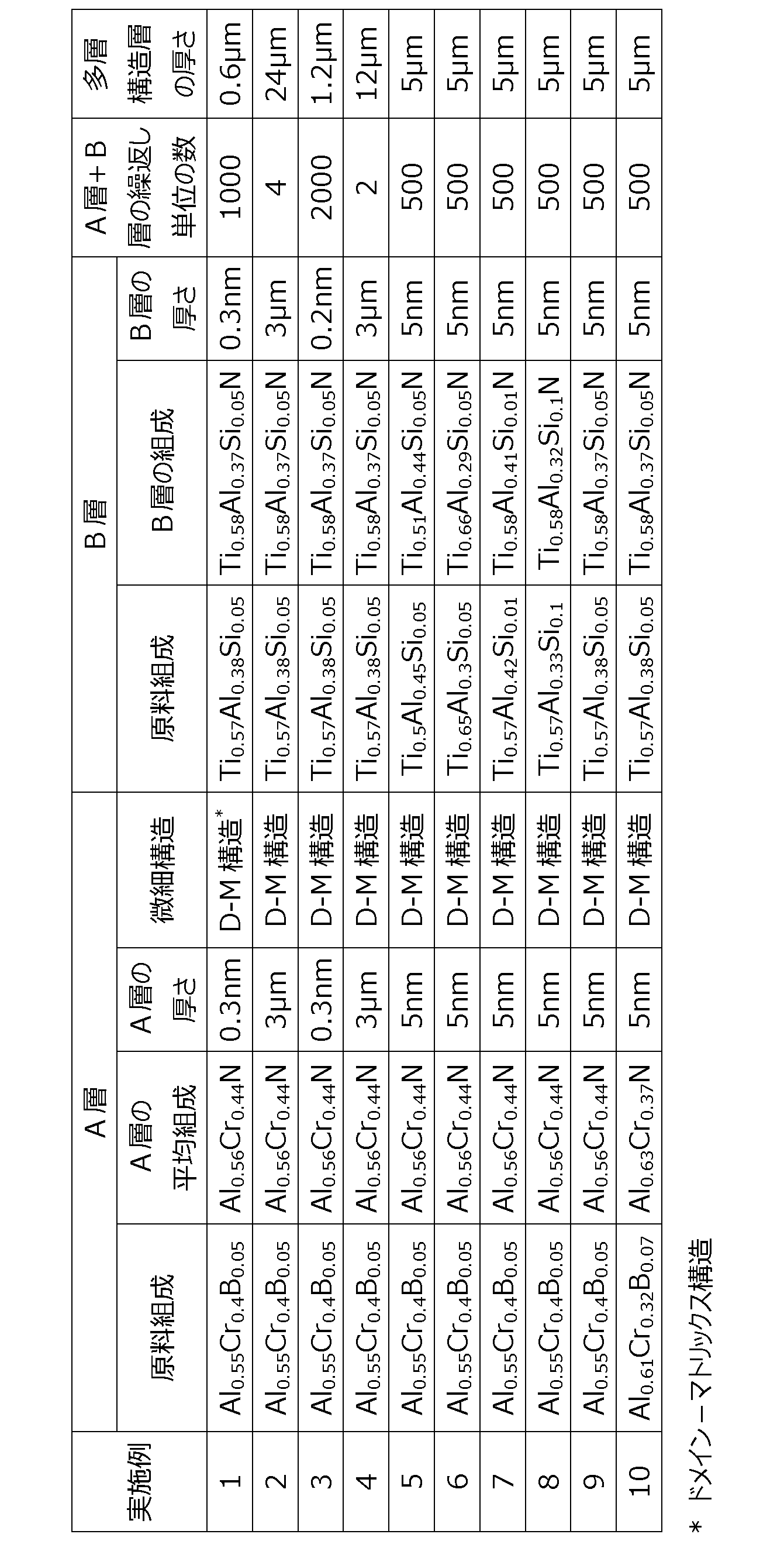
- a coating was prepared by forming a multilayer structure layer including the layers A and B shown in Tables 1 to 3 on the surface of the base material.
- a method for manufacturing the multilayer structure layer will be described.
- a multilayer structure layer having the composition shown was formed.
- the evaporation source for forming the layer A and the evaporation source for forming the layer B those having the raw material compositions shown in Tables 1 to 3 were used.
- the multilayer structure layer was formed by alternately laminating the A layer and the B layer having the compositions shown in Tables 1 to 3 one by one while adjusting the rotation speed of the base material so as to have the thickness shown in Table 1. It produced by doing.
- Comparative Example 1 For Comparative Example 1, a TiN layer was produced as a layer corresponding to the B layer. In Comparative Examples 2 and 10, a TiAlN layer was formed as a layer corresponding to the B layer. In Comparative Examples 1 to 7, the evaporation source for forming the A layer did not contain boron.
- the thickness of the coating (that is, the thickness of the multilayer structure layer) was measured by using a scanning transmission electron microscope (STEM) (trade name: JEM-2100F, manufactured by JEOL Ltd.) in the direction normal to the surface of the substrate. At any 10 points in a cross-sectional sample parallel to the above, and the average value of the measured thicknesses of the 10 points was obtained. The results are shown in Tables 1 to 3.
- the thickness of each of the A layer and the B layer was determined by analysis using EELS. Specifically, in the STEM image obtained by the above measurement, an intensity profile corresponding to Cr and Ti was measured along a direction (region 3b in FIG. 3A) parallel to the laminating direction of the multilayer structure layer. For example, the lower side of FIG. 3B shows the result of the intensity profile obtained by this measurement.
- the intensity profile is a line graph in which the X axis (horizontal axis) is the distance from the measurement start point on the multilayer structure layer, and the Y axis (vertical axis) is the intensity (brightness due to atoms). expressed.
- the distance between the intersections of the line graph corresponding to Cr and the line graph corresponding to Ti was defined as the thickness of each of the A layer and the B layer.
- the distance on the X-axis between the intersections in a portion where the composition ratio of Cr is higher than the composition ratio of Ti is defined as the thickness of the layer A.
- the distance on the X-axis between the intersections in a portion where the composition ratio of Ti is higher than the composition ratio of Cr was defined as the thickness of the B layer.
- the thickness of each layer A and the thickness of each layer B obtained in this way were calculated at least at four places, and the average values were defined as the thickness of the layer A and the thickness of the layer B, respectively. The results are shown in Tables 1 to 3.
- the domain region and the matrix region (the fine structure of the A layer) in the A layer in the multilayer structure layer are determined by a low angle scattering dark field method (LAADF-STEM: Low-Angle Annular Dark-Field Scanning Transmission Electron Microscopy) of a scanning transmission electron microscope.
- LAADF-STEM Low-Angle Annular Dark-Field Scanning Transmission Electron Microscopy
- a cutting tool a surface-coated carbide tip for turning
- the cut surface is polished so that the base material and the coating are included in a length of 2.5 mm ⁇ a width of 0.5 mm ⁇
- a slice having a thickness of 0.1 mm was prepared.
- the section was processed using an ion slicer device (trade name: “IB-09060CIS”, manufactured by JEOL Ltd.) until the section had a thickness of 50 nm or less to obtain a measurement sample. Further, for this measurement sample, for example, a cross-sectional STEM image as shown in FIG. 1A was obtained by analysis using LAADF-STEM. The measurement magnification at this time was 2,000,000 times. In the region 1b of FIG. 1A, it was visually confirmed that the dark region (matrix region) was arranged so as to surround each of the bright regions (domain regions).
- a STEM device (trade name: “JEM-2100F”) manufactured by JEOL Ltd. was used under the conditions of an acceleration voltage of 200 kV.
- the layer A is formed in a direction parallel to the interface between the layer A and the layer B.
- the brightness due to atoms and strains in the A layer with a width of 2 nm was measured as a LAADF intensity profile.
- the lower side of FIG. 1B shows the result of the intensity profile having a width of 2 nm along the measurement direction.
- the intensity profile is expressed as a line graph in which the X axis (horizontal axis) is the distance from the measurement start point on the A layer, and the Y axis (vertical axis) is the intensity (brightness due to atoms). Is done.
- the line graph of FIG. 1B in the cutting tools according to Examples 1 to 21 and Comparative Examples 8 to 13, a repetitive pattern of irregularities was observed in the strength profile in the A layer, and the domain region and the matrix region were different. It was found to be present (Tables 1-3, domain-matrix structure). At this time, it was determined that the peak portion of the LAADF intensity was the domain region and the valley portion of the LAADF intensity was the matrix region.
- the domain region and the matrix region could be more clearly determined.
- the intensity profile corresponding to Cr was measured by EELS along the A layer in a direction parallel to the interface between the A layer and the B layer. The results are shown in FIG. 1C.
- the Cr intensity profile it was determined that a high region was a domain region and a relatively low region was a matrix region.
- ⁇ Analysis of droplets in layer A> The droplets in the layer A were analyzed by the following method. First, a cutting tool (surface-coated carbide tip for turning) was cut, and the cut surface was polished using a focused ion beam device, a cross section polisher device, or the like. Then, the polished cut surface was subjected to composition analysis by EDX attached to a scanning electron microscope. As a result, it was found that in the coatings according to Examples 1 to 21, the droplets in the layer A contained boron.
- ⁇ Average composition of A layer and composition of B layer The average composition of the A layer and the composition of the B layer were calculated by the following methods. The central part of each layer was subjected to line analysis by TEM-EELS (observation magnification: 2,000,000 times), and the composition ratio of Al and Cr was calculated for the A layer, and the composition ratio of Al and Ti was calculated for the B layer. The results are shown in Tables 1 to 3.
- ⁇ Cutting test 2 Drilling test> Using the cutting tools (surface-coated carbide drills) of the samples (Examples 1 to 21 and Comparative Examples 1 to 13) prepared as described above, under the following cutting conditions, the diameter of the hole processed in the workpiece was determined. The number of holes when the dimensional accuracy was out of the specified range (7.99 mm or more and 8.01 mm or less) was counted. The determination of the dimensional accuracy was performed for every 50 holes. The results are shown in Tables 4 and 5. The larger the number of holes, the better the cutting resistance can be evaluated as a cutting tool. Cutting conditions Work material: FCD450 Cutting speed: 100m / min Feed amount: 0.2mm / rev Hole depth: 30mm (through hole), internal lubrication
- ⁇ 1 ⁇ rake face ⁇ 2 ⁇ flank face, ⁇ 3 ⁇ cutting edge ridge, ⁇ 10 ⁇ cutting tool, ⁇ 11 ⁇ substrate, ⁇ 12 ⁇ multilayer structure layer, ⁇ 20 ⁇ coating, ⁇ 31 ⁇ domain area, ⁇ 32 ⁇ matrix area, ⁇ 121 ⁇ A layer, ⁇ 122 ⁇ B layer.
Abstract
Description
したがって、刃先の摩耗及び欠けを抑制することが切削工具の寿命を向上させる上で重要である。 2. Description of the Related Art Conventionally, cutting of steel and castings has been performed using a cutting tool made of a cemented carbide or the like. Such a cutting tool is exposed to a severe environment such as high temperature and high stress at the time of cutting, so that the cutting edge is worn and chipped.
Therefore, it is important to suppress wear and chipping of the cutting edge in order to improve the life of the cutting tool.
基材と、上記基材の表面を被覆する被膜とを備える切削工具であって、
上記被膜は、A層とB層とが基材側から表面側に向かって交互にそれぞれ1層以上積層された多層構造層を含み、
上記A層の平均組成は、AlxCr(1-x)Nであり、
上記B層は、TiyAlzSi(1-y-z)Nからなり、
上記A層は、ドメイン領域とマトリックス領域とからなり、
上記ドメイン領域は、上記マトリックス領域中で複数の部分に分散した状態で存在している領域であり、
上記マトリックス領域は、上記ドメイン領域を構成する上記複数の部分のそれぞれを取り囲むように配置されている領域であり、
上記ドメイン領域におけるCrの組成比は、上記マトリックス領域におけるCrの組成比より高い。ここで、xの範囲は0.5≦x≦0.8であり、yの範囲は0.5≦y<0.71であり、zの範囲は0.29≦z<0.5であり、1-y-zの範囲は0<1-y-z≦0.1である。 Cutting tool according to the present disclosure,
A cutting tool comprising a substrate and a coating covering the surface of the substrate,
The coating includes a multilayer structure layer in which one or more A layers and B layers are alternately laminated from the substrate side to the surface side, respectively.
The average composition of the A layer is Al x Cr (1-x) N,
The B layer is made of Ti y Al z Si (1-yz) N,
The A layer includes a domain region and a matrix region,
The domain region is a region that is present in a state of being dispersed in a plurality of portions in the matrix region,
The matrix region is a region arranged so as to surround each of the plurality of parts constituting the domain region,
The composition ratio of Cr in the domain region is higher than the composition ratio of Cr in the matrix region. Here, the range of x is 0.5 ≦ x ≦ 0.8, the range of y is 0.5 ≦ y <0.71, and the range of z is 0.29 ≦ z <0.5. , 1-yz is such that 0 <1-yz ≦ 0.1.
例えば、特許文献2に記載の耐摩耗皮膜被覆工具は、皮膜にアモルファス層を含むため硬度が低く、切削工具の性能に改善の余地がある。また、当該耐摩耗皮膜被覆工具は、(TiSi)(NB)相を含むため残留応力が高くなる傾向があり、基材と皮膜との密着性に改善の余地がある。 [Problems to be solved by the present disclosure]
For example, the wear-resistant film-coated tool described in
上記によれば、耐摩耗性に優れる切削工具を提供することが可能になる。 [Effects of the present disclosure]
According to the above, it becomes possible to provide a cutting tool having excellent wear resistance.
最初に本開示の実施態様を列記して説明する。 [Description of Embodiment of the Present Disclosure]
First, embodiments of the present disclosure will be listed and described.
基材と、上記基材の表面を被覆する被膜とを備える切削工具であって、
上記被膜は、A層とB層とが基材側から表面側に向かって交互にそれぞれ1層以上積層された多層構造層を含み、
上記A層の平均組成は、AlxCr(1-x)Nであり、
上記B層は、TiyAlzSi(1-y-z)Nからなり、
上記A層は、ドメイン領域とマトリックス領域とからなり、
上記ドメイン領域は、上記マトリックス領域中で複数の部分に分散した状態で存在している領域であり、
上記マトリックス領域は、上記ドメイン領域を構成する上記複数の部分のそれぞれを取り囲むように配置されている領域であり、
上記ドメイン領域におけるCrの組成比は、上記マトリックス領域におけるCrの組成比より高い。ここで、xの範囲は0.5≦x≦0.8であり、yの範囲は0.5≦y<0.71であり、zの範囲は0.29≦z<0.5であり、1-y-zの範囲は0<1-y-z≦0.1である。 [1] The cutting tool according to the present disclosure includes:
A cutting tool comprising a substrate and a coating covering the surface of the substrate,
The coating includes a multilayer structure layer in which one or more A layers and B layers are alternately laminated from the substrate side to the surface side, respectively.
The average composition of the A layer is Al x Cr (1-x) N,
The B layer is made of Ti y Al z Si (1-yz) N,
The A layer includes a domain region and a matrix region,
The domain region is a region that is present in a state of being dispersed in a plurality of portions in the matrix region,
The matrix region is a region arranged so as to surround each of the plurality of parts constituting the domain region,
The composition ratio of Cr in the domain region is higher than the composition ratio of Cr in the matrix region. Here, the range of x is 0.5 ≦ x ≦ 0.8, the range of y is 0.5 ≦ y <0.71, and the range of z is 0.29 ≦ z <0.5. , 1-yz is such that 0 <1-yz ≦ 0.1.
以下、本開示の一実施形態(以下「本実施形態」と記す。)について説明する。ただし、本実施形態はこれに限定されるものではない。本明細書において「A~B」という形式の表記は、範囲の上限下限(すなわちA以上B以下)を意味し、Aにおいて単位の記載がなく、Bにおいてのみ単位が記載されている場合、Aの単位とBの単位とは同じである。さらに、本明細書において、例えば「TiC」等のように、構成元素の組成比が限定されていない化学式によって化合物が表された場合には、その化学式は従来公知のあらゆる組成比(元素比)を含むものとする。このとき上記化学式は、化学量論組成のみならず、非化学量論組成も含むものとする。例えば「TiC」の化学式には、化学量論組成「Ti1C1」のみならず、例えば「Ti1C0.8」のような非化学量論組成も含まれる。このことは、「TiC」以外の化合物の記載についても同様である。 [Details of Embodiment of the Present Disclosure]
Hereinafter, an embodiment of the present disclosure (hereinafter, referred to as “the present embodiment”) will be described. However, the present embodiment is not limited to this. In the present specification, the notation in the form of “A to B” means the upper and lower limits of the range (that is, A or more and B or less), and when a unit is not described in A and a unit is described only in B, A And the unit of B are the same. Further, in the present specification, when a compound is represented by a chemical formula in which the composition ratio of the constituent elements is not limited, such as “TiC”, the chemical formula is represented by any conventionally known composition ratio (element ratio) Shall be included. At this time, the above chemical formula includes not only the stoichiometric composition but also the non-stoichiometric composition. For example, the chemical formula of “TiC” includes not only the stoichiometric composition “Ti 1 C 1 ” but also a non-stoichiometric composition such as “Ti 1 C 0.8 ”. The same applies to the description of compounds other than “TiC”.
本開示に係る切削工具は、
基材と、上記基材の表面を被覆する被膜とを備える切削工具であって、
上記被膜は、A層とB層とが基材側から表面側に向かって交互にそれぞれ1層以上積層された多層構造層を含み、
上記A層の平均組成は、AlxCr(1-x)N(0.5≦x≦0.8)であり、
上記B層は、TiyAlzSi(1-y-z)N(0.5≦y<0.71、0.29≦z<0.5、0<(1-y-z)≦0.1)からなり、
上記A層は、ドメイン領域とマトリックス領域とからなり、
上記ドメイン領域は、上記マトリックス領域中に複数の部分に分かれ、分散した状態で存在している領域であり、
上記マトリックス領域は、上記ドメイン領域を構成する上記複数の領域のそれぞれを取り囲むように配置されている領域であり、
上記ドメイン領域におけるCrの組成比は、上記マトリックス領域におけるCrの組成比より高い。 ≪Surface coated cutting tool≫
Cutting tool according to the present disclosure,
A cutting tool comprising a substrate and a coating covering the surface of the substrate,
The coating includes a multilayer structure layer in which one or more A layers and B layers are alternately laminated from the substrate side to the surface side, respectively.
The average composition of the layer A is Al x Cr (1-x) N (0.5 ≦ x ≦ 0.8),
The B layer is made of Ti y Al z Si (1-yz) N (0.5 ≦ y <0.71, 0.29 ≦ z <0.5, 0 <(1-yz) ≦ 0 .1),
The A layer includes a domain region and a matrix region,
The domain region is a region that is divided into a plurality of portions in the matrix region and exists in a dispersed state,
The matrix region is a region arranged to surround each of the plurality of regions constituting the domain region,
The composition ratio of Cr in the domain region is higher than the composition ratio of Cr in the matrix region.
本実施形態の基材は、この種の基材として従来公知のものであればいずれのものも使用することができる。例えば、上記基材は、超硬合金(例えば、炭化タングステン(WC)基超硬合金、WCの他にCoを含む超硬合金、WCの他にCr、Ti、Ta、Nb等の炭窒化物を添加した超硬合金等)、サーメット(TiC、TiN、TiCN等を主成分とするもの)、高速度鋼、セラミックス(炭化チタン、炭化珪素、窒化珪素、窒化アルミニウム、酸化アルミニウム等)、立方晶型窒化硼素焼結体(cBN焼結体)及びダイヤモンド焼結体からなる群より選ばれる少なくとも1種を含むことが好ましい。上記基材は、超硬合金、サーメット及びcBN焼結体からなる群より選ばれる少なくとも1種を含むことがより好ましい。 <Substrate>
As the substrate of the present embodiment, any conventionally known substrate of this type can be used. For example, the base material is made of a cemented carbide (for example, a tungsten carbide (WC) based cemented carbide, a cemented carbide containing Co in addition to WC, a carbonitride such as Cr, Ti, Ta, Nb in addition to WC) , Cermet (containing TiC, TiN, TiCN, etc. as main components), high-speed steel, ceramics (titanium carbide, silicon carbide, silicon nitride, aluminum nitride, aluminum oxide, etc.), cubic It is preferable to include at least one selected from the group consisting of a sintered boron nitride body (cBN sintered body) and a diamond sintered body. More preferably, the base material includes at least one selected from the group consisting of a cemented carbide, a cermet, and a cBN sintered body.
本実施形態に係る被膜20は、A層121とB層122とが基材11側から表面側に向かって交互にそれぞれ1層以上積層された多層構造層12を含む(例えば、図5)。「被膜」は、上記基材の少なくとも一部(例えば、切削加工時に被削材と接する部分)を被覆することで、切削工具における耐欠損性、耐摩耗性等の諸特性を向上させる作用を有するものである。上記被膜は、上記基材の全面を被覆することが好ましい。しかしながら、上記基材の一部が上記被膜で被覆されていなかったり被膜の構成が部分的に異なっていたりしていたとしても本実施形態の範囲を逸脱するものではない。 <Coating>
The
本実施形態に係る多層構造層は、A層とB層とを含む。上記多層構造層は、上記A層と上記B層とが基材側から表面側に向かって交互にそれぞれ1層以上積層されている。ここで、上記多層構造層12の基材11側は上記A層121から開始することが好ましい(例えば、図5)。このようにすることで、微細構造化したA層の上にB層が積層され、B層の微細構造化が促進される。 (Multilayer structure layer)
The multilayer structure layer according to the present embodiment includes an A layer and a B layer. In the multilayer structure layer, one or more layers of the A layer and the B layer are alternately laminated from the substrate side to the surface side. Here, the
(繰返し単位の数)=(多層構造層の厚さ)/(A層とB層との合計厚さ) In the multilayer structure layer, when the A layer and the B layer constitute one repeating unit, the number of the repeating units is preferably 2 to 10000, more preferably 2 to 3000. The number of repeating units can be calculated, for example, from the following equation.
(Number of repeating units) = (thickness of multilayer structure layer) / (total thickness of A layer and B layer)
本実施形態に係るA層121は、ドメイン領域31とマトリックス領域32とからなる(例えば、図6)。すなわち、上記A層は、微細構造を有する。ここで「ドメイン領域」とは、後述するマトリックス領域中に複数の部分に分かれ、分散した状態で存在している領域を意味する。すなわち、上記ドメイン領域は、上記マトリックス領域中で複数の部分に分散した状態で存在している。また、上記ドメイン領域は、上記A層において複数の領域に分かれて配置される領域と把握することもできる。なお、上述の「分散した状態」は、ドメイン領域が互いに接触しているものを排除するものではない。すなわち、各ドメイン領域は、互いに接していてもよいし、離合していてもよい。 (A layer)
The
本実施形態に係るB層は、TiyAlzSi(1-y-z)N(0.5≦y<0.71、0.29≦z<0.5、0<(1-y-z)≦0.1)からなる。上記B層におけるTiyAlzSi(1-y-z)Nの組成は、上述したA層の平均組成を求める方法と同様の方法によって求めることが可能である。 (B layer)
The layer B according to the present embodiment is composed of Ti y Al z Si (1-yz) N (0.5 ≦ y <0.71, 0.29 ≦ z <0.5, 0 <(1-y− z) ≦ 0.1). The composition of Ti y Al z Si (1-yz) N in the B layer can be obtained by the same method as the above-described method of obtaining the average composition of the A layer.
本実施形態の効果を損なわない範囲において、上記被膜は、他の層を更に含んでいてもよい。上記他の層は、上記多層構造層とは組成が異なっていてもよいし、同じであってもよい。他の層としては、例えば、TiN層、TiCN層、TiBN層、Al2O3層等を挙げることができる。なお、その積層の順も特に限定されない。例えば、上記他の層としては、上記基材と上記多層構造層との間に設けられている下地層、上記多層構造層の上に設けられている最外層等が挙げられる。上記他の層の厚さは、本実施形態の効果を損なわない範囲において、特に制限はないが例えば、0.1μm以上2μm以下が挙げられる。 (Other layers)
As long as the effects of the present embodiment are not impaired, the coating may further include another layer. The composition of the other layers may be different from or the same as the composition of the multilayer structure layer. Examples of other layers include a TiN layer, a TiCN layer, a TiBN layer, an Al 2 O 3 layer, and the like. The order of the lamination is not particularly limited. For example, examples of the other layer include a base layer provided between the base material and the multilayer structure layer, and an outermost layer provided on the multilayer structure layer. The thickness of the other layers is not particularly limited as long as the effects of the present embodiment are not impaired, and is, for example, 0.1 μm or more and 2 μm or less.
本実施形態に係る切削工具の製造方法は、
上記基材を準備する工程(以下、「第1工程」という場合がある。)と、
物理的蒸着法を用いて上記基材の上に上記A層と上記B層とを交互にそれぞれ1層以上積層することによって上記多層構造層を形成する工程(以下、「第2工程」という場合がある。)と、
を含む。 製造 Production method of surface coated cutting tool≫
The manufacturing method of the cutting tool according to the present embodiment,
A step of preparing the base material (hereinafter, may be referred to as a “first step”);
A step of forming the multilayer structure layer by alternately laminating one or more layers of the A layer and the B layer on the base material using a physical vapor deposition method (hereinafter referred to as a “second step”) There is.)
including.
第1工程では基材を準備する。例えば、基材として超硬合金基材が準備される。超硬合金基材は、市販のものを用いてもよく、一般的な粉末冶金法で製造してもよい。一般的な粉末冶金法で製造する場合、例えば、ボールミル等によってWC粉末とCo粉末等とを混合して混合粉末を得る。該混合粉末を乾燥した後、所定の形状に成形して成形体を得る。さらに該成形体を焼結することにより、WC-Co系超硬合金(焼結体)を得る。次いで該焼結体に対して、ホーニング処理等の所定の刃先加工を施すことにより、WC-Co系超硬合金からなる基材を製造することができる。第1工程では、上記以外の基材であっても、この種の基材として従来公知のものであればいずれも準備可能である。 <First step: Step of preparing base material>
In the first step, a base material is prepared. For example, a cemented carbide substrate is prepared as a substrate. The cemented carbide substrate may be a commercially available one, or may be manufactured by a general powder metallurgy method. When manufacturing by a general powder metallurgy method, for example, a WC powder and a Co powder are mixed by a ball mill or the like to obtain a mixed powder. After the mixed powder is dried, it is molded into a predetermined shape to obtain a molded body. Further, by sintering the compact, a WC-Co-based cemented carbide (sintered body) is obtained. Next, by subjecting the sintered body to a predetermined cutting edge such as honing, a base material made of a WC-Co-based cemented carbide can be manufactured. In the first step, any substrate other than those described above can be prepared as long as it is a conventionally known substrate of this type.
第2工程では、A層とB層とが交互にそれぞれ1層以上積層された多層構造層が形成される。その方法としては、形成しようとするA層及びB層の組成に応じて、各種の方法が用いられる。例えば、Ti、Cr、Al、Si及びホウ素等の粒径をそれぞれ変化させた合金製ターゲットを使用する方法、それぞれ組成の異なる複数のターゲットを使用する方法、成膜時に印可するバイアス電圧をパルス電圧とする方法、成膜時にガス流量を変化させる方法、又は、成膜装置において基材を保持する基材ホルダの回転速度を調整する方法等を挙げることができる。これらの方法を組み合わせて多層構造層を形成することもできる。 <Second step: Step of forming a multilayer structure layer>
In the second step, a multilayer structure layer is formed in which one or more A layers and B layers are alternately laminated. As the method, various methods are used depending on the composition of the A layer and the B layer to be formed. For example, a method using an alloy target in which the particle diameters of Ti, Cr, Al, Si, boron, etc. are respectively changed, a method using a plurality of targets each having a different composition, a bias voltage applied at the time of film formation and a pulse voltage , A method of changing the gas flow rate during film formation, or a method of adjusting the rotation speed of the substrate holder that holds the substrate in the film forming apparatus. These methods can be combined to form a multilayer structure layer.
なお、ホウ素は通常、金属元素と非金属元素との中間の性質を示す半金属として捉えられるが、本実施形態においては、自由電子を有する元素を金属であるとみなしてホウ素を金属元素の範囲に含むものとする。 The content ratio (atomic ratio) of boron is preferably 0.01 or more and less than 0.1, and more preferably 0.03 or more and 0.07 or less, when the whole raw material of the A layer is 1. More preferably, it is 0.03 or more and 0.05 or less. By setting the content ratio of boron in this way, the domain region and the matrix region are formed efficiently. Further, the A layer having high hardness can be formed.
Note that boron is generally regarded as a metalloid having an intermediate property between a metal element and a nonmetal element. However, in the present embodiment, boron is regarded as an element having free electrons as a metal, and boron is regarded as a metal element. Shall be included.
本実施形態に係る製造方法では、上述した工程の他にも、基材と上記多層構造層との間に下地層を形成する下地層被覆工程、上記多層構造層の上に最外層を形成する最外層被覆工程及び表面処理する工程等を適宜行ってもよい。上述の下地層及び最外層等の他の層を形成する場合、従来の方法によって他の層を形成してもよい。具体的には、例えば、上述したPVD法によって上記他の層を形成することが挙げられる。表面処理をする工程としては、例えば、応力を付与する弾性材にダイヤモンド粉末を担持させたメディアを用いた表面処理等が挙げられる。上記表面処理を行う装置としては、例えば、株式会社不二製作所製のシリウスZ等が挙げられる。 <Other steps>
In the manufacturing method according to the present embodiment, in addition to the above-described steps, an underlayer coating step of forming an underlayer between the substrate and the multilayer structure layer, and forming an outermost layer on the multilayer structure layer An outermost layer coating step, a surface treatment step, and the like may be appropriately performed. When forming other layers such as the above-described underlayer and outermost layer, other layers may be formed by a conventional method. Specifically, for example, the above-mentioned other layer is formed by the above-mentioned PVD method. As the step of performing the surface treatment, for example, a surface treatment using a medium in which a diamond powder is supported on an elastic material for applying a stress and the like can be mentioned. As an apparatus for performing the surface treatment, for example, Sirius Z manufactured by Fuji Manufacturing Co., Ltd. and the like can be mentioned.
(付記1)
基材と、前記基材の表面を被覆する被膜とを備える表面被覆切削工具であって、
前記被膜は、A層とB層とが基材側から表面側に向かって交互にそれぞれ1層以上積層された多層構造層を含み、
前記A層の平均組成は、AlxCr(1-x)N(0.5≦x≦0.8)であり、
前記B層は、TiyAlzSi(1-y-z)N(0.5≦y<0.71、0.29≦z<0.5、0<(1-y-z)≦0.1)からなり、
前記A層は、ドメイン領域とマトリックス領域とからなり、
前記ドメイン領域は、前記マトリックス領域中に複数の部分に分かれ、分散した状態で存在している領域であり、
前記マトリックス領域は、前記ドメイン領域を構成する前記複数の領域のそれぞれを取り囲むように配置されている領域であり、
前記ドメイン領域におけるCrの組成比は、前記マトリックス領域におけるCrの組成比より高い、表面被覆切削工具。
(付記2)
前記A層は、その厚さが0.2nm以上3μm以下である、付記1に記載の表面被覆切削工具。
(付記3)
前記B層は、その厚さが0.2nm以上3μm以下である、付記1又は付記2に記載の表面被覆切削工具。
(付記4)
前記多層構造層は、その厚さが0.5μm以上30μm以下である、付記1から付記3のいずれかに記載の表面被覆切削工具。 The above description includes the features described below.
(Appendix 1)
A substrate, a surface-coated cutting tool comprising a coating for coating the surface of the substrate,
The coating includes a multilayer structure layer in which one or more A layers and B layers are alternately stacked from the substrate side to the surface side, respectively.
The average composition of the A layer is Al x Cr (1-x) N (0.5 ≦ x ≦ 0.8),
The B layer is composed of Ti y Al z Si (1-yz) N (0.5 ≦ y <0.71, 0.29 ≦ z <0.5, 0 <(1-yz) ≦ 0 .1),
The A layer includes a domain region and a matrix region,
The domain region is a region that is divided into a plurality of portions in the matrix region and exists in a dispersed state,
The matrix region is a region arranged so as to surround each of the plurality of regions constituting the domain region,
A surface-coated cutting tool, wherein a composition ratio of Cr in the domain region is higher than a composition ratio of Cr in the matrix region.
(Appendix 2)
The surface-coated cutting tool according to claim 1, wherein the A layer has a thickness of 0.2 nm or more and 3 μm or less.
(Appendix 3)
The surface-coated cutting tool according to
(Appendix 4)
The surface-coated cutting tool according to any one of supplementary notes 1 to 3, wherein the multilayer structure layer has a thickness of 0.5 μm or more and 30 μm or less.
<基材の準備>
まず、被膜を形成させる対象となる基材として、旋削加工用超硬チップ(JIS規格 K30相当超硬合金、CNMG120408N-GU)及び超硬ドリル(外径8mm、JIS規格 K10相当超硬合金、MDW0800HGS5)を準備した(基材を準備する工程)。 ≫Making cutting tools≫
<Preparation of base material>
First, as a base material on which a coating is formed, a carbide tip for turning (a cemented carbide equivalent to JIS K30, CNMG120408N-GU) and a carbide drill (outer diameter 8 mm, a cemented carbide equivalent to JIS K10, MDW0800HGS5) ) Was prepared (step of preparing a base material).
上記基材の表面上に、表1~表3に示されるA層及びB層を含む多層構造層を形成することによって、被膜を作製した。以下、多層構造層の作製方法について説明する。 <Preparation of coating>
A coating was prepared by forming a multilayer structure layer including the layers A and B shown in Tables 1 to 3 on the surface of the base material. Hereinafter, a method for manufacturing the multilayer structure layer will be described.
実施例1~21及び比較例1~13においては、基材(旋削加工用超硬チップ及び超硬ドリル)をチャンバ内の中央で回転させた状態で、反応ガスとして窒素を導入した。さらに、基材を温度500℃に、反応ガス圧を2.0Paに、バイアス電源の電圧を-30V~-800Vの範囲の一定値にそれぞれ維持し、又はそれぞれを徐々に変化させながらA層形成用の蒸発源及びB層形成用の蒸発源にそれぞれ100Aのアーク電流を供給した。これにより、A層形成用の蒸発源及びB層形成用の蒸発源からそれぞれ金属イオンを発生させ、所定の時間が経過したところでアーク電流の供給を止めて、基材の表面上に表1に示す組成の多層構造層を形成した。ここで、A層形成用の蒸発源及びB層形成用の蒸発源は、それぞれ表1~3に記載の原料組成のものを用いた。このとき多層構造層は、表1~3に示す組成を有するA層及びB層を、表1に示す厚さを有するように基材の回転速度を調整しながら、それぞれ1層ずつ交互に積層することによって作製した。 (Preparation of multilayer structure layer)
In Examples 1 to 21 and Comparative Examples 1 to 13, nitrogen was introduced as a reaction gas in a state where the base material (the turning carbide tip and the carbide drill) was rotated in the center of the chamber. Further, the base layer is maintained at a temperature of 500 ° C., the reaction gas pressure is maintained at 2.0 Pa, the voltage of the bias power supply is maintained at a constant value in a range of −30 V to −800 V, or the A layer is formed while gradually changing each. Arc current of 100 A was supplied to each of the evaporation source for forming the layer B and the evaporation source for forming the layer B. As a result, metal ions are generated from the evaporation source for forming the layer A and the evaporation source for forming the layer B, respectively, and after a predetermined time has elapsed, the supply of the arc current is stopped. A multilayer structure layer having the composition shown was formed. Here, as the evaporation source for forming the layer A and the evaporation source for forming the layer B, those having the raw material compositions shown in Tables 1 to 3 were used. At this time, the multilayer structure layer was formed by alternately laminating the A layer and the B layer having the compositions shown in Tables 1 to 3 one by one while adjusting the rotation speed of the base material so as to have the thickness shown in Table 1. It produced by doing.


上述のようにして作製した試料(実施例1~21及び比較例1~13)の切削工具(旋削加工用表面被覆超硬チップ)を用いて、以下のように、切削工具の各特性を評価した。なお、表面被覆超硬ドリルも同一のチャンバ内で被膜を形成したことから、対応する旋削加工用表面被覆超硬チップと同様の特性を有していると考えられる。 特性 Evaluation of cutting tool characteristics≫
Using the cutting tools (surface-coated carbide tips for turning) of the samples (Examples 1 to 21 and Comparative Examples 1 to 13) produced as described above, the characteristics of the cutting tools were evaluated as follows. did. Since the surface-coated carbide drill also formed the coating in the same chamber, it is considered that the surface-coated carbide drill has the same characteristics as the corresponding surface-coated carbide tip for turning.
被膜の厚さ(すなわち、多層構造層の厚さ)は、走査透過型電子顕微鏡(STEM)(日本電子株式会社製、商品名:JEM-2100F)を用いて、基材の表面の法線方向に平行な断面サンプルにおける任意の10点を測定し、測定された10点の厚さの平均値をとることで求めた。結果を表1~表3に示す。 <Measurement of film thickness (thickness of multilayer structure layer)>
The thickness of the coating (that is, the thickness of the multilayer structure layer) was measured by using a scanning transmission electron microscope (STEM) (trade name: JEM-2100F, manufactured by JEOL Ltd.) in the direction normal to the surface of the substrate. At any 10 points in a cross-sectional sample parallel to the above, and the average value of the measured thicknesses of the 10 points was obtained. The results are shown in Tables 1 to 3.
A層及びB層それぞれの厚さは、EELSを用いた分析によって求めた。具体的には、上述の測定によって得られたSTEM像において、上記多層構造層の積層方向に平行な方向(図3Aの領域3b)に沿ってCrとTiとに対応する強度プロファイルを測定した。例えば、図3Bの下側には、この測定によって得られた上記強度プロファイルの結果を示している。図3Bにおいて上記強度プロファイルは、X軸(横軸)を上記多層構造層上の測定開始点からの距離とし、Y軸(縦軸)を強度(原子に起因する明るさ)とした折れ線グラフとして表される。得られたグラフにおいて、Crに対応する折れ線グラフと、Tiに対応する折れ線グラフとの交点間の距離をA層及びB層それぞれの厚さとした。ここで、CrはA層にのみ存在することから、Crの組成比がTiの組成比よりも高い部分における当該交点間のX軸における距離をA層の厚さとした。また、Tiの組成比がCrの組成比よりも高い部分における当該交点間のX軸における距離をB層の厚さとした。このようにして求められた各A層の厚さ及び各B層の厚さそれぞれを少なくとも4カ所算出し、それぞれの平均値をA層の厚さ及びB層の厚さとした。結果を表1~3に示す。 <Measurement of thickness of A layer and B layer>
The thickness of each of the A layer and the B layer was determined by analysis using EELS. Specifically, in the STEM image obtained by the above measurement, an intensity profile corresponding to Cr and Ti was measured along a direction (
上述の測定で求められた多層構造層の厚さ、A層及びB層それぞれの厚さに基づいて、以下の式からA層及びB層の積層回数(繰返し単位の数)を算出した。
(繰返し単位の数)=(多層構造層の厚さ)/(A層とB層との合計厚さ)
求められた繰返し単位の数を表1~3に示す。 <Lamination number of A layer and B layer (number of repeating units)>
Based on the thickness of the multilayer structure layer and the thicknesses of the A layer and the B layer determined by the above-described measurement, the number of laminations of the A layer and the B layer (the number of repeating units) was calculated from the following equation.
(Number of repeating units) = (thickness of multilayer structure layer) / (total thickness of A layer and B layer)
Tables 1 to 3 show the determined number of repeating units.
多層構造層におけるA層におけるドメイン領域及びマトリックス領域(A層の微細構造)は、走査透過型電子顕微鏡の低角度散乱暗視野法(LAADF-STEM:Low-Angle Annular Dark-Field Scanning Transmission Electron Microscopy)を用いた分析によってそれぞれ特定した。具体的には、まず切削工具(旋削加工用表面被覆超硬チップ)を切断し、その切断面を研磨することにより、基材と被膜とが含まれる長さ2.5mm×幅0.5mm×厚さ0.1mmの切片を作製した。この切片に対し、イオンスライサ装置(商品名:「IB-09060CIS」、日本電子株式会社製)を用い、切片の厚さが50nm以下となるまで加工することにより測定試料を得た。さらに、この測定試料に対し、LAADF-STEMを用いた分析によって例えば、図1Aに示すような断面STEM像を得た。このときの測定倍率は、200万倍であった。図1Aの領域1bにおいて、暗い領域(マトリックス領域)が明るい領域(ドメイン領域)のそれぞれを取り囲むように配置されていることが視覚的に確認できた。ここで、LAADF-STEMを用いた分析には、日本電子株式会社製のSTEM装置(商品名:「JEM-2100F」)を加速電圧200kVの条件下で用いた。 <Domain region and matrix region in A layer (microstructure of A layer)>
The domain region and the matrix region (the fine structure of the A layer) in the A layer in the multilayer structure layer are determined by a low angle scattering dark field method (LAADF-STEM: Low-Angle Annular Dark-Field Scanning Transmission Electron Microscopy) of a scanning transmission electron microscope. Each was identified by analysis using. Specifically, first, a cutting tool (a surface-coated carbide tip for turning) is cut, and the cut surface is polished so that the base material and the coating are included in a length of 2.5 mm × a width of 0.5 mm × A slice having a thickness of 0.1 mm was prepared. The section was processed using an ion slicer device (trade name: “IB-09060CIS”, manufactured by JEOL Ltd.) until the section had a thickness of 50 nm or less to obtain a measurement sample. Further, for this measurement sample, for example, a cross-sectional STEM image as shown in FIG. 1A was obtained by analysis using LAADF-STEM. The measurement magnification at this time was 2,000,000 times. In the
A層におけるドロップレットの分析を以下の方法で行った。まず切削工具(旋削加工用表面被覆超硬チップ)を切断し、その切断面を集束イオンビーム装置、クロスセクションポリッシャ装置等を用いて研磨した。その後、研磨された当該切断面について、走査電子顕微鏡に付帯のEDXで組成分析した。
その結果、実施例1~21に係る被膜では、A層におけるドロップレットにホウ素が含まれることが分かった。 <Analysis of droplets in layer A>
The droplets in the layer A were analyzed by the following method. First, a cutting tool (surface-coated carbide tip for turning) was cut, and the cut surface was polished using a focused ion beam device, a cross section polisher device, or the like. Then, the polished cut surface was subjected to composition analysis by EDX attached to a scanning electron microscope.
As a result, it was found that in the coatings according to Examples 1 to 21, the droplets in the layer A contained boron.
A層の平均組成、及びB層の組成を以下の方法で算出した。各層の中央部をTEM-EELS(観察倍率200万倍)で線分析し、A層についてはAlとCrとの組成比を、B層についてはAlとTiの組成比を算出した。結果を表1~3に示す。 <Average composition of A layer and composition of B layer>
The average composition of the A layer and the composition of the B layer were calculated by the following methods. The central part of each layer was subjected to line analysis by TEM-EELS (observation magnification: 2,000,000 times), and the composition ratio of Al and Cr was calculated for the A layer, and the composition ratio of Al and Ti was calculated for the B layer. The results are shown in Tables 1 to 3.
<切削試験1:旋削加工試験>
上述のようにして作製した試料(実施例1~21、比較例1~13)の切削工具(旋削加工用表面被覆超硬チップ)を用いて、以下の切削条件により逃げ面摩耗量(Vb)が0.2mmとなるまでの切削距離を測定した。その結果を表4及び表5に示す。切削距離が長いほど耐摩耗性に優れる切削工具として評価することができる。
切削条件
被削材 :FCD700
切削速度 :200m/min
送り量 :0.15mm/rev
切込み量(ap):2mm、dry ≪Cutting test≫
<Cutting test 1: Turning test>
Using the cutting tool (surface coated carbide tip for turning) of the sample (Examples 1 to 21 and Comparative Examples 1 to 13) produced as described above, the flank wear (Vb) under the following cutting conditions: Was measured until 0.2 mm was obtained. The results are shown in Tables 4 and 5. A longer cutting distance can be evaluated as a cutting tool having more excellent wear resistance.
Cutting conditions Work material: FCD700
Cutting speed: 200m / min
Feed amount: 0.15mm / rev
Cutting depth (ap): 2 mm, dry
上述のようにして作製した試料(実施例1~21、比較例1~13)の切削工具(表面被覆超硬ドリル)を用いて、以下の切削条件により、被加工材における加工された穴の寸法精度が規定の範囲(7.99mm以上8.01mm以下)を外れた時点の穴数を計数した。上記寸法精度の判定は、50穴ごとに実施した。その結果を表4及び表5に示す。穴数が多いほど耐摩耗性に優れる切削工具として評価することができる。
切削条件
被削材 :FCD450
切削速度 :100m/min
送り量 :0.2mm/rev
穴深さ :30mm(貫通穴)、内部給油 <Cutting test 2: Drilling test>
Using the cutting tools (surface-coated carbide drills) of the samples (Examples 1 to 21 and Comparative Examples 1 to 13) prepared as described above, under the following cutting conditions, the diameter of the hole processed in the workpiece was determined. The number of holes when the dimensional accuracy was out of the specified range (7.99 mm or more and 8.01 mm or less) was counted. The determination of the dimensional accuracy was performed for every 50 holes. The results are shown in Tables 4 and 5. The larger the number of holes, the better the cutting resistance can be evaluated as a cutting tool.
Cutting conditions Work material: FCD450
Cutting speed: 100m / min
Feed amount: 0.2mm / rev
Hole depth: 30mm (through hole), internal lubrication

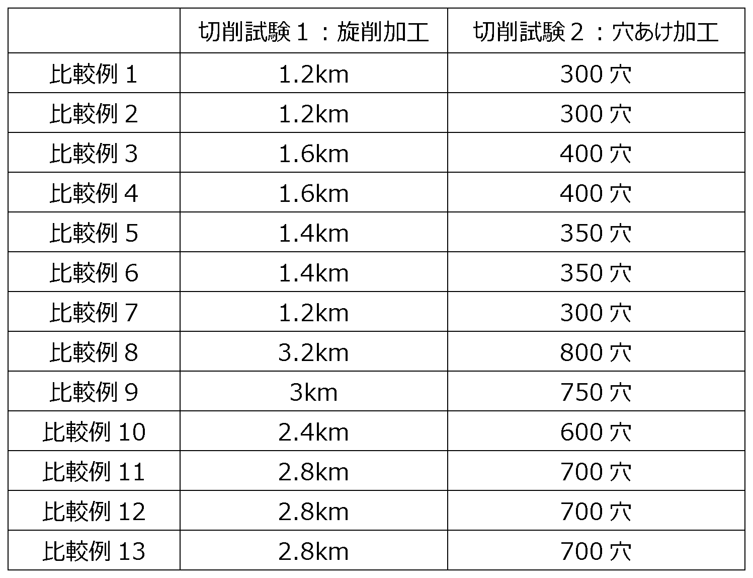
Claims (4)
- 基材と、前記基材の表面を被覆する被膜とを備える切削工具であって、
前記被膜は、A層とB層とが基材側から表面側に向かって交互にそれぞれ1層以上積層された多層構造層を含み、
前記A層の平均組成は、AlxCr(1-x)Nであり、
前記B層は、TiyAlzSi(1-y-z)Nからなり、
前記A層は、ドメイン領域とマトリックス領域とからなり、
前記ドメイン領域は、前記マトリックス領域中で複数の部分に分散した状態で存在している領域であり、
前記マトリックス領域は、前記ドメイン領域を構成する前記複数の部分のそれぞれを取り囲むように配置されている領域であり、
前記ドメイン領域におけるCrの組成比は、前記マトリックス領域におけるCrの組成比より高い、切削工具。
ここで、xの範囲は0.5≦x≦0.8であり、yの範囲は0.5≦y<0.71であり、zの範囲は0.29≦z<0.5であり、1-y-zの範囲は0<1-y-z≦0.1である。 A cutting tool comprising a substrate and a coating covering the surface of the substrate,
The coating includes a multilayer structure layer in which one or more A layers and B layers are alternately stacked from the substrate side to the surface side, respectively.
The average composition of the A layer is Al x Cr (1-x) N,
The B layer is made of Ti y Al z Si (1-yz) N,
The A layer includes a domain region and a matrix region,
The domain region is a region that exists in a dispersed state in a plurality of portions in the matrix region,
The matrix region is a region arranged so as to surround each of the plurality of portions constituting the domain region,
A cutting tool, wherein the composition ratio of Cr in the domain region is higher than the composition ratio of Cr in the matrix region.
Here, the range of x is 0.5 ≦ x ≦ 0.8, the range of y is 0.5 ≦ y <0.71, and the range of z is 0.29 ≦ z <0.5. , 1-yz is such that 0 <1-yz ≦ 0.1. - 前記A層の厚さが0.2nm以上3μm以下である、請求項1に記載の切削工具。 The cutting tool according to claim 1, wherein the thickness of the layer A is 0.2 nm or more and 3 μm or less.
- 前記B層の厚さが0.2nm以上3μm以下である、請求項1又は請求項2に記載の切削工具。 The cutting tool according to claim 1 or 2, wherein the thickness of the B layer is 0.2 nm or more and 3 μm or less.
- 前記多層構造層の厚さが0.5μm以上30μm以下である、請求項1から請求項3のいずれか一項に記載の切削工具。 4. The cutting tool according to claim 1, wherein a thickness of the multilayer structure layer is 0.5 μm or more and 30 μm or less. 5.
Priority Applications (5)
| Application Number | Priority Date | Filing Date | Title |
|---|---|---|---|
| JP2019566859A JP6743349B2 (en) | 2018-08-24 | 2019-06-26 | Cutting tools |
| CN201980038481.6A CN112262006B (en) | 2018-08-24 | 2019-06-26 | Cutting tool |
| EP19851641.1A EP3842169A4 (en) | 2018-08-24 | 2019-06-26 | Cutting tool |
| KR1020207034766A KR20210003913A (en) | 2018-08-24 | 2019-06-26 | Cutting tool |
| US16/636,785 US11524339B2 (en) | 2018-08-24 | 2019-06-26 | Cutting tool |
Applications Claiming Priority (2)
| Application Number | Priority Date | Filing Date | Title |
|---|---|---|---|
| JP2018-157419 | 2018-08-24 | ||
| JP2018157419 | 2018-08-24 |
Publications (1)
| Publication Number | Publication Date |
|---|---|
| WO2020039736A1 true WO2020039736A1 (en) | 2020-02-27 |
Family
ID=69592587
Family Applications (1)
| Application Number | Title | Priority Date | Filing Date |
|---|---|---|---|
| PCT/JP2019/025275 WO2020039736A1 (en) | 2018-08-24 | 2019-06-26 | Cutting tool |
Country Status (6)
| Country | Link |
|---|---|
| US (1) | US11524339B2 (en) |
| EP (1) | EP3842169A4 (en) |
| JP (1) | JP6743349B2 (en) |
| KR (1) | KR20210003913A (en) |
| CN (1) | CN112262006B (en) |
| WO (1) | WO2020039736A1 (en) |
Citations (8)
| Publication number | Priority date | Publication date | Assignee | Title |
|---|---|---|---|---|
| JP2002331408A (en) | 2001-05-11 | 2002-11-19 | Hitachi Tool Engineering Ltd | Abrasion resistant coating film-covered tool |
| JP2004050381A (en) * | 2002-07-24 | 2004-02-19 | Mitsubishi Materials Corp | Cutting tool made of surface covering cemented carbide in which hard covering layer exhibits excellent chipping resistance at deep cutting processing condition |
| WO2006070730A1 (en) | 2004-12-28 | 2006-07-06 | Sumitomo Electric Hardmetal Corp. | Surface-coated cutting tool and process for producing the same |
| JP2011011286A (en) * | 2009-07-01 | 2011-01-20 | Sumitomo Electric Hardmetal Corp | Surface coated cutting tool |
| JP2012166333A (en) * | 2011-01-27 | 2012-09-06 | Mitsubishi Materials Corp | Surface-coated cutting tool having excellent chipping and wear resistance |
| JP2016199793A (en) * | 2015-04-13 | 2016-12-01 | 株式会社神戸製鋼所 | Hard film |
| JP2017154200A (en) * | 2016-02-29 | 2017-09-07 | 三菱マテリアル株式会社 | Surface-coated cutting tool |
| JP2018157419A (en) | 2017-03-17 | 2018-10-04 | 株式会社東芝 | Receiver |
Family Cites Families (11)
| Publication number | Priority date | Publication date | Assignee | Title |
|---|---|---|---|---|
| DE60336453D1 (en) * | 2002-01-21 | 2011-05-05 | Mitsubishi Materials Corp | "SURFACE-COATED CUTTING UNIT WITH A HARD COATING LAYER HAVING EXCELLENT FRICTION CUT RESISTANCE IN HIGH-SPEED CUTTING, AND METHOD FOR FORMING THE HARD COATING LAYER ON THE CUTTING TOOL SURFACE" |
| WO2006070509A1 (en) | 2004-12-28 | 2006-07-06 | Sumitomo Electric Hardmetal Corp. | Surface-coated cutting tool and process for producing the same |
| US7348074B2 (en) * | 2005-04-01 | 2008-03-25 | Oc Oerlikon Balzers Ag | Multilayer hard coating for tools |
| US7947363B2 (en) * | 2007-12-14 | 2011-05-24 | Kennametal Inc. | Coated article with nanolayered coating scheme |
| JP5061394B2 (en) * | 2008-10-31 | 2012-10-31 | 住友電工ハードメタル株式会社 | Surface coated cutting tool |
| EP2336383A1 (en) * | 2009-12-04 | 2011-06-22 | Sandvik Intellectual Property AB | Multilayered coated cutting tool |
| JP2011167794A (en) * | 2010-02-18 | 2011-09-01 | Mitsubishi Materials Corp | Surface coated cutting tool |
| JP5459506B2 (en) * | 2010-08-09 | 2014-04-02 | 三菱マテリアル株式会社 | Surface coated cutting tool |
| DE112013003182B4 (en) * | 2012-06-29 | 2022-05-25 | Sumitomo Electric Hardmetal Corp. | Surface coated cutting tool |
| JP2017080879A (en) * | 2015-10-28 | 2017-05-18 | 三菱マテリアル株式会社 | Surface coated cutting tool |
| CN107740045A (en) * | 2017-10-10 | 2018-02-27 | 岭南师范学院 | A kind of nickel base superalloy processing coated cutting tool and preparation method thereof |
-
2019
- 2019-06-26 US US16/636,785 patent/US11524339B2/en active Active
- 2019-06-26 KR KR1020207034766A patent/KR20210003913A/en not_active Application Discontinuation
- 2019-06-26 EP EP19851641.1A patent/EP3842169A4/en active Pending
- 2019-06-26 CN CN201980038481.6A patent/CN112262006B/en active Active
- 2019-06-26 WO PCT/JP2019/025275 patent/WO2020039736A1/en unknown
- 2019-06-26 JP JP2019566859A patent/JP6743349B2/en active Active
Patent Citations (8)
| Publication number | Priority date | Publication date | Assignee | Title |
|---|---|---|---|---|
| JP2002331408A (en) | 2001-05-11 | 2002-11-19 | Hitachi Tool Engineering Ltd | Abrasion resistant coating film-covered tool |
| JP2004050381A (en) * | 2002-07-24 | 2004-02-19 | Mitsubishi Materials Corp | Cutting tool made of surface covering cemented carbide in which hard covering layer exhibits excellent chipping resistance at deep cutting processing condition |
| WO2006070730A1 (en) | 2004-12-28 | 2006-07-06 | Sumitomo Electric Hardmetal Corp. | Surface-coated cutting tool and process for producing the same |
| JP2011011286A (en) * | 2009-07-01 | 2011-01-20 | Sumitomo Electric Hardmetal Corp | Surface coated cutting tool |
| JP2012166333A (en) * | 2011-01-27 | 2012-09-06 | Mitsubishi Materials Corp | Surface-coated cutting tool having excellent chipping and wear resistance |
| JP2016199793A (en) * | 2015-04-13 | 2016-12-01 | 株式会社神戸製鋼所 | Hard film |
| JP2017154200A (en) * | 2016-02-29 | 2017-09-07 | 三菱マテリアル株式会社 | Surface-coated cutting tool |
| JP2018157419A (en) | 2017-03-17 | 2018-10-04 | 株式会社東芝 | Receiver |
Non-Patent Citations (2)
| Title |
|---|
| C. TRITREMMEL ET AL.: "Mechanical and tribological properties of Al-Ti-N/Al-Cr-B-N multilayer films synthesized by cathodic arc evaporation", SURFACE & COATINGS TECHNOLOGY, vol. 246, 2014, pages 57 - 63, XP028839537, DOI: 10.1016/j.surfcoat.2014.03.005 |
| See also references of EP3842169A4 |
Also Published As
| Publication number | Publication date |
|---|---|
| JP6743349B2 (en) | 2020-08-19 |
| CN112262006A (en) | 2021-01-22 |
| US20210086268A1 (en) | 2021-03-25 |
| EP3842169A4 (en) | 2021-12-15 |
| JPWO2020039736A1 (en) | 2020-08-27 |
| CN112262006B (en) | 2023-07-25 |
| EP3842169A1 (en) | 2021-06-30 |
| US11524339B2 (en) | 2022-12-13 |
| KR20210003913A (en) | 2021-01-12 |
Similar Documents
| Publication | Publication Date | Title |
|---|---|---|
| US7901796B2 (en) | Coated cutting tool and manufacturing method thereof | |
| CN108883481B (en) | Coated cutting tool | |
| CN110944776B (en) | Coated cutting tool | |
| WO2012043459A1 (en) | Cutting tool | |
| CN110691662B (en) | Coated cutting tool | |
| JP5404232B2 (en) | Cutting tools | |
| JPWO2018216256A1 (en) | Coatings and cutting tools | |
| JP6794604B1 (en) | Cutting tools | |
| WO2019035219A1 (en) | Coated cutting tool | |
| JP5241538B2 (en) | Cutting tools | |
| WO2020039736A1 (en) | Cutting tool | |
| WO2020039735A1 (en) | Cutting tool | |
| JP4844879B2 (en) | Surface coated cutting tool with excellent wear resistance with hard coating layer in high speed cutting of heat resistant alloy | |
| JP2021030356A (en) | Surface-coated cutting tool | |
| JP2008030159A (en) | Surface coat cutting tool having hard coating layer exhibiting excellent chipping resistance and wear resistance in high-speed heavy-cutting of heat-resistant alloy | |
| WO2020213263A1 (en) | Cutting tool | |
| WO2022239139A1 (en) | Cutting tool | |
| JP7338827B1 (en) | Cutting tools | |
| JP2011110653A (en) | Cutting tool | |
| JP2005022045A (en) | Cutting tool made of surface coated cemented carbide with hard coating layer exhibiting excellent wear resistance in high-speed cutting | |
| JP2005022046A (en) | Cutting tool made of surface coated cemented carbide with hard coating layer exhibiting excellent wear resistance in high-speed cutting |
Legal Events
| Date | Code | Title | Description |
|---|---|---|---|
| ENP | Entry into the national phase |
Ref document number: 2019566859 Country of ref document: JP Kind code of ref document: A |
|
| 121 | Ep: the epo has been informed by wipo that ep was designated in this application |
Ref document number: 19851641 Country of ref document: EP Kind code of ref document: A1 |
|
| ENP | Entry into the national phase |
Ref document number: 20207034766 Country of ref document: KR Kind code of ref document: A |
|
| NENP | Non-entry into the national phase |
Ref country code: DE |
|
| ENP | Entry into the national phase |
Ref document number: 2019851641 Country of ref document: EP Effective date: 20210324 |