WO2020031972A1 - 結合インダクタおよびスイッチング回路 - Google Patents
結合インダクタおよびスイッチング回路 Download PDFInfo
- Publication number
- WO2020031972A1 WO2020031972A1 PCT/JP2019/030760 JP2019030760W WO2020031972A1 WO 2020031972 A1 WO2020031972 A1 WO 2020031972A1 JP 2019030760 W JP2019030760 W JP 2019030760W WO 2020031972 A1 WO2020031972 A1 WO 2020031972A1
- Authority
- WO
- WIPO (PCT)
- Prior art keywords
- core
- coupled inductor
- inductor
- joint
- phase
- Prior art date
Links
Images


Classifications
-
- H—ELECTRICITY
- H01—ELECTRIC ELEMENTS
- H01F—MAGNETS; INDUCTANCES; TRANSFORMERS; SELECTION OF MATERIALS FOR THEIR MAGNETIC PROPERTIES
- H01F1/00—Magnets or magnetic bodies characterised by the magnetic materials therefor; Selection of materials for their magnetic properties
- H01F1/01—Magnets or magnetic bodies characterised by the magnetic materials therefor; Selection of materials for their magnetic properties of inorganic materials
- H01F1/03—Magnets or magnetic bodies characterised by the magnetic materials therefor; Selection of materials for their magnetic properties of inorganic materials characterised by their coercivity
- H01F1/12—Magnets or magnetic bodies characterised by the magnetic materials therefor; Selection of materials for their magnetic properties of inorganic materials characterised by their coercivity of soft-magnetic materials
- H01F1/14—Magnets or magnetic bodies characterised by the magnetic materials therefor; Selection of materials for their magnetic properties of inorganic materials characterised by their coercivity of soft-magnetic materials metals or alloys
- H01F1/20—Magnets or magnetic bodies characterised by the magnetic materials therefor; Selection of materials for their magnetic properties of inorganic materials characterised by their coercivity of soft-magnetic materials metals or alloys in the form of particles, e.g. powder
- H01F1/22—Magnets or magnetic bodies characterised by the magnetic materials therefor; Selection of materials for their magnetic properties of inorganic materials characterised by their coercivity of soft-magnetic materials metals or alloys in the form of particles, e.g. powder pressed, sintered, or bound together
- H01F1/24—Magnets or magnetic bodies characterised by the magnetic materials therefor; Selection of materials for their magnetic properties of inorganic materials characterised by their coercivity of soft-magnetic materials metals or alloys in the form of particles, e.g. powder pressed, sintered, or bound together the particles being insulated
-
- H—ELECTRICITY
- H01—ELECTRIC ELEMENTS
- H01F—MAGNETS; INDUCTANCES; TRANSFORMERS; SELECTION OF MATERIALS FOR THEIR MAGNETIC PROPERTIES
- H01F27/00—Details of transformers or inductances, in general
- H01F27/24—Magnetic cores
-
- H—ELECTRICITY
- H01—ELECTRIC ELEMENTS
- H01F—MAGNETS; INDUCTANCES; TRANSFORMERS; SELECTION OF MATERIALS FOR THEIR MAGNETIC PROPERTIES
- H01F27/00—Details of transformers or inductances, in general
- H01F27/24—Magnetic cores
- H01F27/255—Magnetic cores made from particles
-
- H—ELECTRICITY
- H01—ELECTRIC ELEMENTS
- H01F—MAGNETS; INDUCTANCES; TRANSFORMERS; SELECTION OF MATERIALS FOR THEIR MAGNETIC PROPERTIES
- H01F3/00—Cores, Yokes, or armatures
- H01F3/08—Cores, Yokes, or armatures made from powder
-
- H—ELECTRICITY
- H01—ELECTRIC ELEMENTS
- H01F—MAGNETS; INDUCTANCES; TRANSFORMERS; SELECTION OF MATERIALS FOR THEIR MAGNETIC PROPERTIES
- H01F37/00—Fixed inductances not covered by group H01F17/00
Definitions
- the present invention relates to a coupling inductor and a switching circuit having the coupling inductor.
- the interleave method has attracted attention as a circuit method for achieving high power density.
- the interleave method is a control method in which a power supply is divided into a plurality of systems, each phase has a phase difference, and ripples and the like are canceled each other. For example, in a two-phase interleaving method, a ripple is offset by giving a 180 ° phase difference to the current phase. By employing the interleaving method, it is possible to reduce the size and weight of the output smoothing capacitor and to reduce the ripple.
- the interleave method the number of components of the inductor increases, so that there is a limit in increasing the power density. Therefore, in addition to the interleaving method, the use of a coupling inductor that magnetically couples and uses inductors of each phase is being studied. The following effects are expected by using a coupled inductor.
- the number of inductors equal to the number of paralleled phases increases, but by using a coupled inductor, the windings of each phase can be integrated into a single magnetic core. Therefore, the number of parts can be reduced.
- the core size is largely related to the maximum magnetic flux in the core.
- DC magnetic fluxes generated from DC currents of windings are mutually canceled while parallel inductors are used. Since the alternating magnetic flux generated between the integrated circuits can be shared, the magnetic flux in the core can be reduced, and the size of the inductor can be reduced.
- an object of the present invention is to provide a small three-phase coupled inductor having stable performance as a coupled inductor.
- the present invention is used in an interleaved three-phase switching circuit, and includes a coupling inductor having a core and three windings magnetically coupled to each other. Is wound, three legs arranged equally in the circumferential direction, a first joint that joins one end of each leg, and a second joint that joins the other end of each leg.
- the core is not provided with an air gap and the core is formed of a soft magnetic powder with an insulating coating.
- the leakage magnetic flux is more likely to be generated as compared with the case where ferrite is used as the core material. Therefore, an appropriate leakage flux can be generated in the entire core without providing an air gap. Further, it is not necessary to separately provide a path through which the leakage magnetic flux flows. Therefore, it is possible to reduce the size of the three-phase coupled inductor while preventing heat generation in the winding.
- the initial magnetic permeability of the soft magnetic powder with an insulating coating is preferably 30 or more and 200 or less.
- the coupling coefficient is preferably 0.3 or more and 0.85 or less.
- the press load when forming the first joint and the second joint can be reduced, and the manufacturing equipment can be downsized. it can.
- a small three-phase coupled inductor having stable performance as a coupled inductor can be provided.
- FIG. 4 is a plan view of the coupled inductor in a state where a first junction is removed, as viewed from the first junction.
- FIG. 2 is a perspective view illustrating a shape of a core when a winding is removed from the coupled inductor 1 illustrated in FIG. 1.
- FIG. 3 is a circuit diagram illustrating an interleaved three-phase boost chopper circuit. It is a top view showing the flow of the magnetic flux in the 1st junction in the coupling inductor of this embodiment. It is a top view showing other embodiments of a coupling inductor. It is a top view showing other embodiments of a coupling inductor.
- FIG. 10 is a perspective view showing another reference example of the three-phase coupled inductor.
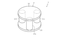
- FIG. 1 is a perspective view of the coupled inductor 1 according to the present embodiment
- FIG. 2 is a view of the coupled inductor 1 in a state where a later-described first joint 22 is removed, as viewed from the first joint 22 side.
- FIG. 1 As shown in FIGS. 1 and 2, the coupled inductor 1 has a core 2 and three windings 31a to 31c.
- the core 2 has legs 21a to 21c, and first and second joints 22 and 23 having the same shape and separated in the direction of the winding axis of the windings 31a to 31c.
- the first joint 22 joins one ends of the legs 21a to 21c
- the second joint 23 joins the other ends of the legs 21a to 21c.
- the leg portions 21a to 21c are formed in a columnar shape
- the first joint portion 22 and the second joint portion 23 are formed in a disk shape having the same diameter and the same thickness. Except for the three legs 21a to 21c, no other legs serving as magnetic flux paths are provided between the first joint 22 and the second joint 23.
- the leg portions 21a to 21c are arranged in a circumferential direction between the first joint portion 22 and the second joint portion 23 coaxially arranged on the center O such that the central angle ⁇ is 120 °. They are arranged in parallel to each other in an evenly distributed manner.
- FIG. 3 is a perspective view showing the shape of the core 2 when the windings 31a to 31c are removed from the coupled inductor 1 shown in FIG. As shown in FIG. 3, the core 2 is integrated such that both end surfaces of the legs 21a to 21c are in contact with the end surfaces of the first joint 22 and the second joint 23. The core 2 does not have an air gap.
- the legs 21a to 21c, the first joint 22 and the second joint 23 constituting the core 2 are all manufactured by compression molding soft magnetic powder and then performing annealing.
- the soft magnetic powder it is preferable to use a soft magnetic powder with an insulating coating obtained by coating an insulating coating made of a resin or the like on a soft magnetic metal powder of a pure iron type, an amorphous type, a soft magnetic alloy type, a nanocrystalline type or the like.
- the initial magnetic permeability (meaning the relative magnetic permeability at a magnetic field of 0 A / m) of the soft magnetic powder with the insulating coating is preferably 30 or more and 200 or less.
- the core 2 also has the same initial magnetic permeability as the magnetic powder before compression molding.
- the material of the core 2 it is preferable to use only the soft magnetic powder described above and not to use a mixed material obtained by mixing the soft magnetic powder and the resin powder.
- the leg portions 21a to 21c, the first joint portion 22, and the second joint portion 23 may be formed of the same material or different materials.
- winding 31a to 31c is attached to each leg 21a to 21c.
- Each of the windings 31a to 31c has the same number of turns, is formed of the same conductive material, and has the same cross-sectional dimension. Therefore, each of the windings 31a to 31c has the same inductance.
- the windings 31a to 31c are connected and arranged so as to have the same polarity. Specifically, as shown in FIG. 2, when a direct current (direction of an arrow in the drawing) flows in both windings 31a to 31c in the same direction, a magnetic flux (for example, FIG. 2, the windings 31a to 31c are connected to the circuit so as to generate a magnetic flux directed toward the front side in the vertical direction of FIG.
- the windings 31a to 31c wound in advance are attached to the outer periphery of each of the legs 21a to 21c. And then fix the second joint 23 to the other end of each of the legs 21a to 21c.
- Each of the legs 21a to 21c is fixed to the first joint 21 and the second joint by, for example, bonding.
- the coupling coefficient of the coupling inductor 1 be set in a range of 0.3 to 0.85 (preferably, 0.3 to 0.75).
- the use of the soft magnetic powder with the insulating coating as the material of the core 2 makes it easy to adjust the coupling coefficient, and it is possible to easily obtain a coupling coefficient within this range.
- the coupling coefficient here is obtained from the following equation based on the open / short method specified in JIS C 5321.
- Coupling coefficient k ⁇ 1-Lsc / Lop ⁇ 1/2
- Lsc is a short-circuit L value (all other lines are short-circuited)
- Lop is an open L value.
- FIG. 4 shows a schematic configuration of a DC-DC three-phase boost chopper circuit as an example of the switching circuit.
- each of the windings 31a to 31c of the coupled inductor 1 is connected to the power source E in parallel.
- the other end of the winding 31a is connected to the anode of the first diode D1 and one end of the first switching element Q1
- the other end of the winding 31b is connected to the anode of the second diode D2 and one end of the second switching element Q2. Is done.
- the other end of the winding 31c is connected to the anode of the third diode D3 and one end of the third switching element Q3.
- the other ends of the switching elements Q1 to Q3 are connected to the ground.
- Each of the switching elements Q1 to Q3 repeats the opening / closing operation at a constant cycle according to a control signal from a control device (not shown). At this time, the switching elements Q1 to Q3 repeat the opening / closing operation by shifting the phase by 120 °.
- the voltage and current output from the cathodes of the diodes D1 to D3 are smoothed by the smoothing capacitor C and consumed by the load R.
- the input current can be divided and the capacity can be further increased as compared with the case of two phases. Further, the capacity of the output-side smoothing capacitor can be further reduced.
- FIG. 5 is a plan view showing the flow of the magnetic flux at the first junction 22 in the coupled inductor 1 of the present embodiment. As shown in the figure, during the operation of the coupled inductor 1, DC magnetic fluxes (indicated by broken arrows) generated from the inductor average current cancel each other out.
- AC magnetic fluxes ⁇ ab , ⁇ ba , ⁇ bc , ⁇ cb , ⁇ ac , ⁇ ca can be shared by any combination of these to strengthen or cancel each other out to make a magnetic flux path. Circulate. As described above, the DC magnetic flux cancels each other, thereby reducing the magnetic flux in the core. On the other hand, a magnetic flux path through which the magnetic flux of the AC component circulates is formed, so that the inductance of the coupling inductor 1 increases. Therefore, the magnetic flux generated in the core 2 can be reduced, and the core 2 can be downsized. As a result, the ripple width can be reduced and the superimposition characteristics can be improved.
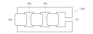
- the three-phase coupled inductor it is conceivable to use a four-leg type planar structure core 200 as shown in FIG. This is provided with three legs for winding the winding 301 and one leg having an air gap G1 for securing a path for leakage magnetic flux.
- this core structure the distance between the windings 301 and the magnetic path length of the path through which the leakage magnetic flux of each phase flows are different, and the symmetry is lacking. There is a difference. Therefore, there is a problem in that the performance of the coupled in inductor is deteriorated.
- a three-dimensional core structure shown in FIG. 11 can be considered (reference example).
- a core is provided with three outer legs 210 displaced from each other by 120 ° and a center leg 211 having an air gap G2, and a winding 310 is wound around each of the three outer legs 210.
- the center leg 211 is used as a path of the leakage magnetic flux.
- the magnetic flux does not cancel each other, and the magnetic flux flows into the central leg 211 (indicated by an arrow in the figure). Therefore, the diameter of the central leg 211 is increased due to the necessity of preventing magnetic saturation. I have to do it. Therefore, there is a limit in reducing the size of the coupling inductor.
- the core 2 is formed using soft magnetic powder with an insulating coating having an initial magnetic permeability of 30 to 200, ferrite (an initial magnetic permeability of 2300 to 2500) which is a general core material is used. Leakage magnetic flux is more likely to occur than in the case of using ()). Therefore, even if the central leg 211 shown in FIG. 11 is omitted, an appropriate leakage flux can be generated in the entire core 2. This makes it possible to reduce the size of the coupled inductor 1 while achieving the ripple suppressing effect and the improvement of the DC current superposition characteristics.
- FIGS. 6A to 6D are plan views of the coupled inductor 1 as viewed from the first joint portion 22 side.
- the embodiment shown in FIGS. 6A to 6D differs from the embodiment shown in FIGS. 1 and 2 in the core structure, but the other configurations are common.
- FIG. 6A shows an example in which the first joint portion 22 and the second joint portion 23 are formed in a perforated disk shape having a hole 24 at the center in the embodiment shown in FIG. 1, and FIG. An example in which the portion 22 and the second joining portion 23 are formed in a triangular plate shape is shown.
- FIG. 6C shows an example in which a hole 24 is provided at the center of the first joint portion 22 and the second joint portion 23 in the embodiment of FIG. 6B
- FIG. 6D shows that the first joint portion 22 and the second joint portion 23 are formed. This is an example in which it is formed in a shape extending radially from the center.
- FIGS. 6A to 6D the entire end surfaces of the three pillar portions 21a to 21c arranged at equal positions are covered by the first joint portion 22 and the second joint portion 23. .
- the coupled inductor 1 shown in FIG. 1 was used as an example.
- an inductor 1 ' was used in which the two windings 31b and 31c were removed from the coupled inductor of the first embodiment.
- the inductance value was measured from the current flowing when a voltage having a phase difference of 120 ° was applied to the three windings 31a, 31b, 31c.
- the inductance value when an alternating current was applied was measured.
- the core 2 in the example and the comparative example is formed of a soft magnetic powder with an insulating coating (initial magnetic permeability of 70) using an amorphous material as a soft magnetic material.
- V in and V out in both equations represent the input voltage and the output voltage in the inductors of the example and the comparative example. Further, d represents a duty ratio, ⁇ I represents a ripple current width, and f represents a switching frequency (50 kHz).
- the coupled inductor 1 is arranged in the boost chopper circuit has been described as an example.
- the coupled inductor 1 described above can be used in any circuit having an interleaved two-phase switching circuit.
- the present invention can be used for power transformation (for both step-down and step-up) in a PFC (power factor correction) circuit, a converter circuit, an inverter circuit, and the like, an inverter application, a converter application, and the like.
Landscapes
- Engineering & Computer Science (AREA)
- Power Engineering (AREA)
- Chemical & Material Sciences (AREA)
- Dispersion Chemistry (AREA)
- Dc-Dc Converters (AREA)
- Soft Magnetic Materials (AREA)
Abstract
結合インダクタ1は、インターリーブ方式の3相のスイッチング回路に用いられ、コア2と、互いに磁気結合した3つの巻線31a~31cを有する。コア2は、それぞれに巻線31a~31cが巻回され、周方向に等配して配置された3つの脚部21a~21cと、各脚部の一端を接合する第一接合部22と、各脚部の他端を接合する第二接合部23とを有する。コア2にエアギャップは設けない。
Description
本発明は、結合インダクタおよび当該結合インダクタを有するスイッチング回路に関する。
近年、蓄電池を内蔵した輸送機器(例えばハイブリッドカー、電気自動車、燃料電池車等)や電子機器(例えばスマートフォン、パーソナルコンピュータ等)の電力変換回路は高出力を維持した上で小型軽量化、すなわち高電力密度化が求められている。
高電力密度化を実現する回路方式としてインターリーブ方式が注目されている。インターリーブ方式は電源を複数系統に分けて各相に位相差を持たせ、リップルなどを互いに打ち消し合う制御方式である。例えば2相のインターリーブ方式では、電流位相に180°の位相差をもたせてリップルを相殺する。インターリーブ方式を採用することにより、出力平滑コンデンサの小型軽量化やリップルの低減を図ることができる。
その一方で、インターリーブ方式では、インダクタの部品点数が増加するため、高電力密度化には限界がある。そこで、インターリーブ方式に加えて、各相のインダクタを磁気的に結合して利用する結合インダクタを採用することが検討されている。結合インダクタを使用する事で以下の効果が期待される。
(1)従来のインターリーブ方式では並列化させた相数に等しい数のインダクタが増加することになるが、結合インダクタを用いることで、各相の巻線を単一の磁性体コアに集約させることができるため、部品点数の削減が可能となる。
(2)一般的にコアサイズはコア内の最大磁束が大きく関係するが、逆結合で磁気的に結合させた結合インダクタでは、巻線の直流電流から発生する直流磁束を互いに打ち消す一方で、並列化させた回路間で発生する交流磁束を共有できるため、コア内の磁束を低減でき、インダクタのサイズ低減を図ることができる。
以上に述べた結合インダクタの一例として、二つのE形状コアと、二つのE形状コアで挟まれ、二つのコイルが巻回されたI形状コアと、一方のE形状コアの中央脚とI形状コアとの間に設けられた第1ギャップと、他方のE形状コアの中央脚とI形状コアとの間に設けられた第2ギャップとを有する2相結合インダクタ(下記特許文献1)が知られている。
近年では、特許文献1に記載された2相インターリーブ用の結合インダクタを3相のインターリーブ回路でも使用することが検討されている。3相に拡張することで、2相の場合と比べて、入力電流を分流化できるため更なる大容量化が実現できる。また、出力側平滑コンデンサの容量をさらに低減することも可能となる。
しかしながら、3相のインターリーブ回路に適合する結合インダクタの検証は十分に進んでいない。例えば特許文献1に記載の2相結合インダクタのコアに、もう一つの脚を追加したとしても、各相の磁路長を同じにすることができず、磁束の偏りや各相での損失のアンバランスが生じる。従って、結合インダクタとしての性能が低下する。
そこで、本発明は、結合インダクタとして安定した性能を有する小型の3相結合インダクタを提供することを目的とする。
以上の課題を解決するため、本発明は、インターリーブ方式の3相のスイッチング回路に用いられ、コアと、互いに磁気結合した3つの巻線とを有する結合インダクタにおいて、前記コアが、それぞれに巻線が巻回され、周方向に等配して配置された3つの脚部と、各脚部の一端を接合する第一接合部と、各脚部の他端を接合する第二接合部とを有し、前記コアにエアギャップが設けられておらず、かつ前記コアが絶縁被膜付き軟磁性粉末で形成されていることを特徴とする。
このように、絶縁被膜付き軟磁性粉末を使用してコアを形成することにより、コア材料としてフェライトを使用する場合に比べ、漏れ磁束が発生し易くなる。従って、エアギャップを設けなくても、コア全体で適度の漏れ磁束を発生させることができる。また、漏れ磁束が流れる経路を別途設ける必要がない。従って、巻線での発熱を防止しつつ、3相結合インダクタの小型化を図ることができる。
絶縁被膜付き軟磁性粉末の初透磁率は30以上、200以下が好ましい。
結合係数は0.3以上、0.85以下が好ましい。
第一接合部および第二接合部の中心に孔を設けておけば、第一接合部および第二接合部を成形する際のプレス荷重を低減することができ、製造設備を小型化することができる。
以上に述べた結合インダクタを使用して、インターリーブ方式の3相のスイッチング回路を形成することにより、回路の高電力密度化を達成することができる。
本発明によれば、結合インダクタとして安定した性能を有する小型の3相結合インダクタを提供することができる。
以下、本発明の実施形態を図面に基づいて説明する。
図1は、本実施形態に係る結合インダクタ1の斜視図であり、図2は、後述する第一接合部22を取り外した状態の当該結合インダクタ1を、第一接合部22側から見た時の平面図である。
図1および図2に示すように、この結合インダクタ1は、コア2と、3つの巻線31a~31cを有する。
図1および図2に示すように、この結合インダクタ1は、コア2と、3つの巻線31a~31cを有する。
図1に示すように、コア2は、脚部21a~21cと、巻線31a~31cの巻線軸方向に離間した同形状の第一接合部22および第二接合部23とを有する。第一接合部22は脚部21a~21cの各一端を接合し、第二接合部23は、脚部21a~21cの各他端を接合する。この実施形態において、脚部21a~21cは円柱状に形成され、第一接合部22および第二接合部23は同径および同肉厚の円板状に形成されている。第一接合部22と第二接合部23の間には、3つの脚部21a~21cを除き、磁束経路となるような他の脚部は設けられていない。
図2に示すように、脚部21a~21cは、中心O上に同軸配置した第一接合部22および第二接合部23の間に、中心角θが120°となるように円周方向に等配した形で互いに平行に配置される。
各脚部21a~21cの両端面は、それらの領域全てが第一接合部22および第二接合部で覆われている。これは、不要な磁束漏れを極力抑えるためである。かかる効果を得るため、図1および図2の実施形態では、第一接合部22および第二接合部23の外周面の輪郭が脚部21a~21cの両端面に対して外接円を構成している(特に図2参照)。この他、第一接合部22および第二接合部23を、その直径が上記外接円の直径よりも大きくなるように形成しても同様の効果が得られる。
図3は、図1に示す結合インダクタ1から巻線31a~31cを取り除いた時のコア2の形状を示す斜視図である。
図3に示すように、コア2は、脚部21a~21cの両端面を全て第一接合部22および第二接合部23の端面に接触させた状態で一体化されている。コア2には、エアギャップは設けられていない。
図3に示すように、コア2は、脚部21a~21cの両端面を全て第一接合部22および第二接合部23の端面に接触させた状態で一体化されている。コア2には、エアギャップは設けられていない。
コア2を構成する脚部21a~21c、第一接合部22および第二接合部23は、何れも軟磁性粉末を圧縮成形した後、焼鈍処理を施すことで製作される。軟磁性粉末としては、純鉄系、アモルファス系、軟磁性合金系、ナノ結晶系等の軟磁性金属粉末に樹脂等からなる絶縁被膜をコーティングした絶縁被膜付き軟磁性粉末を使用するのが好ましい。この絶縁被膜付き軟磁性粉末の初透磁率(磁界0 A/m時の比透磁率を意味する)は、30以上200以下が好ましい。熱処理として焼鈍が行われ、焼結は行われないため、熱処理後のコア2の軟磁性粉末は、絶縁被膜でコーティングされた当初の形態を保持する。従って、コア2も圧縮成形前の磁性粉末と同程度の初透磁率を有する。コア2の材料としては、上記の軟磁性粉末のみを使用し、当該軟磁性粉末と樹脂粉末とを混合した混合材は使用しないのが好ましい。また、脚部21a~21c、第一接合部22、および第二接合部23を同じ材料で形成する他、異なる材料で形成することもできる。
各脚部21a~21cには、それぞれ一つずつ巻線31a~31cが装着される。各巻線31a~31cの巻き数は同じであり、同じ導電材料で形成され、かつ同じ断面寸法を有する。従って、各巻線31a~31cは等しいインダクタンスを有する。また、各巻線31a~31cは同極性となるように接続および配置される。具体的には、図2に示すように、両巻線31a~31cに同方向の直流電流(図中矢印方向)を流した際に、各脚部21a~21cに同方向の磁束(例えば図2の紙面鉛直方向手前側に向かう磁束)が生じるように各巻線31a~31cが回路に接続される。
以上に述べた結合インダクタ1は、例えば、第一接合部22に各脚部21a~21cの一端部を固定した状態で、予め巻回した巻線31a~31cを各脚部21a~21cの外周に挿入し、その後、各脚部21a~21cの他端部に第二接合部23を固定することによって製作される。各脚部21a~21cは、第一接合部21および第二接合部に対し、例えば接着によって固定される。
このようにして製作した結合インダクタ1では、漏れインダクタンスを利用する必要があるため、結合係数を高くしすぎないことが必要となる。もちろん結合係数が低すぎれば、磁気結合による効果を得ることができない。以上の観点から、結合インダクタ1の結合係数は、0.3~0.85(好ましくは0.3~0.75)の範囲に設定するのが好ましい。上記のとおりコア2の材料として絶縁被膜付き軟磁性粉末を使用することで、結合係数の調整が容易となり、この範囲内の結合係数を容易に得ることが可能となる。なお、ここでの結合係数は、JIS C 5321に規定された開放短絡法に基づいた、以下の式から求められる。
結合係数k={1-Lsc/Lop}1/2
ここで、Lscは短絡L値(他線全てを短絡)であり、Lopは開放L値である。
結合係数k={1-Lsc/Lop}1/2
ここで、Lscは短絡L値(他線全てを短絡)であり、Lopは開放L値である。
以上に述べた結合インダクタ1は、図4に示す、インターリーブ方式を採用した3相のスイッチング回路に配置される。ここでいうスイッチング回路は、スイッチングに伴って高周波電流が流れる回路を意味する。図4では、スイッチング回路の一例として、DC-DC3相昇圧チョッパ回路の概略構成を示している。
図4に示すように、電源Eには、結合インダクタ1における各巻線31a~31cの一端が並列に接続される。巻線31aの他端は、第一ダイオードD1のアノードおよび第一スイッチング素子Q1の一端と接続され、巻線31bの他端は、第二ダイオードD2のアノードおよび第二スイッチング素子Q2の一端と接続される。巻線31cの他端は、第三ダイオードD3のアノードおよび第三スイッチング素子Q3の一端と接続される。各スイッチング素子Q1~Q3の他端は接地側に接続される。各スイッチング素子Q1~Q3は、図示しない制御装置からの制御信号により一定周期で開閉動作を繰り返す。この時、各スイッチング素子Q1~Q3は120°ずつ位相をずらして開閉動作を繰り返す。
各ダイオードD1~D3のカソードから出力された電圧および電流は平滑用コンデンサCにより平滑化され、負荷Rにより消費される。
昇圧チョッパ回路を単体で構成するシングルフェーズ方式の場合、出力側の平滑用コンデンサに送られる電流が断続的となるため、平滑用コンデンサは激しい充電と放電を繰り返す。そのため、平滑用コンデンサに大きな容量が必要となり、平滑用コンデンサが大型化する。これに対し、回路を並列化して動作させる図4のインターリーブ方式(マルチフェーズ方式)では、各相を交互にスイッチングさせるように制御を行うため、平滑用コンデンサCの蓄積電荷変動が低減され、平滑用コンデンサCの小型化を達成することができる。
加えて、インターリーブ回路を3相に拡張しているので、2相の場合と比べて、入力電流を分流化できるため更なる大容量化が実現できる。また、出力側平滑コンデンサの容量をさらに低減することも可能となる。
また、結合インダクタ1では、各相のインダクタを磁気的に相互結合し、等価的に一つのインダクタで昇圧動作を行うことができる。図5は、本実施形態の結合インダクタ1における第一接合部22での磁束の流れを示す平面図である。同図に示すように、結合インダクタ1の動作中は、インダクタ平均電流から発生する直流磁束(破線矢印で示す)が相互に打ち消し合う。その一方で、交流磁束φab,φba,φbc,φcb,φac,φca(実線矢印で示す)は、これらの任意の組合せで共有して強め合い、あるいは打消し合って磁束経路を循環する。このように、直流磁束を互いに打消し合うことでコア内磁束を低減できる一方で、交流成分の磁束が循環する磁束経路が形成されるため、結合インダクタ1のインダクタンスが大きくなる。従って、コア2に発生する磁束を減らしてコア2を小型化することができる。これによりリプル幅を小さくすると共に、重畳特性を良化することができる。
また、コア2の磁束経路にエアギャップが形成されていないため、漏れ磁束が小さくなる。従って、漏れ磁束が巻線31a~31cに到達し、各巻線で渦電流を生じることによる巻線31a~31cの発熱を防止することができる。またインダクタンスの低下も防止することができる。これにより小型でありながら巻線31a~31cでの発熱の小さい結合インダクタ1を提供することが可能となる。
次に、本実施形態にかかる3相結合インダクタ1の優位性を、他に想定される3相結合インダクタ(参考例)との対比で説明する。
3相結合インダクタの単純形態として、図10に示すように、4脚型平面構造のコア200を用いることも考えられる。これは、巻線301を巻回するための3つの脚に加え、漏れ磁束の経路を確保するためにエアギャップG1を有する1つの脚を設けたものである。しかしながら、このコア構造では、巻線301間の距離や各相の漏れ磁束が流れる経路の磁路長が異なっており、対称性を欠くため、各相均一にすべき漏れインダクタンスや相互インダクタンスに大きな差が生じる。そのため、結合インインダクタの性能劣化を招く点が問題となる。
この問題を解決する3相結合インダクタとして、図11に示す立体構造のコア構造が考えられる(参考例)。この結合インダクタは、コアに、120°位置をずらして配置した3つの外側脚210と、エアギャップG2を有する中央脚211とを設け、3つの外側脚210にそれぞれ巻線310を巻回すると共に、中央脚211を漏れ磁束の経路として使用するものである。しかしながら、このコア構造では、磁束の打ち消し合いが生じず、中央脚211に磁束が流れ込む(図中の矢印で示す)構造であるため、磁気飽和を防止する必要性から中央脚211を大径化せざるを得ない。そのため結合インダクタの小型化を図るには限界がある。
これに対し、本実施形態では、初透磁率30~200の絶縁被膜付き軟磁性粉末を使用してコア2を形成しているので、一般的なコア材料であるフェライト(初透磁率2300~2500)を使用する場合に比べ、漏れ磁束が発生し易い。従って、図11に示す中央脚211を省略してもコア2全体で適度の漏れ磁束を発生させることができる。これによりリプル抑制効果と直流電流重畳特性の良化とを達成しつつ、結合インダクタ1の小型化を図ることが可能となる。
また、フェライトをコア材料とした場合、フェライトの初透磁率が高いため、漏れ磁束が少なくなる。そのため、インダクタを大型化しないとリプル幅を抑制できず、小型化の要請に応えることができない。漏れ磁束を多くするためには磁束経路にエアギャップ(図10の符号G1、図11の符号G2参照)を設けるのが有効であるが、これでは既に述べたように巻線31a~31cでの発熱の問題を生じる。
これに対し、本実施形態のように、初透磁率30~200の絶縁被膜付き軟磁性粉末を使用してコア2を形成することにより、エアギャップを設けない場合でも適度の結合係数(0.30~0.85)を得ることができる。そのため、エアギャップを設けた場合に問題となる巻線31a~31cでの発熱を防止しつつ、安定したリプル抑制効果および直流電流重畳特性を有する小型の結合インダクタ1を提供することができる。
次に、3相結合インダクタ1の他の実施形態を図6A~図6Dに基づいて説明する。図6A~図6Dに示す実施形態は、何れも結合インダクタ1を第一接合部22側から見た平面図である。図6A~図6Dに示す実施形態は、図1および図2に示す実施形態とコア構造を異にするが、その他の構成は共通する。
図6Aは、図1に示す実施形態において、第一接合部22および第二接合部23を、中心に孔24を有する孔開き円板状に形成した例を示し、図6Bは、第一接合部22および第二接合部23を三角板状に形成した例を示す。図6Cは、図6Bの実施形態において、第一接合部22および第二接合部23の中心に孔24を設けた例を示し、図6Dは、第一接合部22および第二接合部23を、中心から放射状に延びた形状に形成した例である。図6A~図6Dから明らかなように、等配位置に配置された3つの柱部21a~21cの両端面は、その全領域が第一接合部22および第二接合部23によって覆われている。
なお、図6Aおよび図6Cに示すように、第一接合部22および第二接合部23の中心に孔24を設けることにより、第1接合部22および第二接合部23を成形する際のプレス荷重を低減することが可能となる。
次に本実施形態に係る結合インダクタ1について、その効果を確認する確認試験を行ったので、その詳細および結果を説明する。
実施例として図1に示す結合インダクタ1を使用した。また、比較例として、図7に示すように、実施例1の結合インダクタから、2つの巻線31b,31cを取り除いたインダクタ1’を使用した。実施例については3つの巻線31a,31b,31cに位相差120°の電圧を印加した時の通電電流よりインダクタンス値を測定した。比較例については、交流電流を通電した時のインダクタンス値を測定した。また、それぞれ直流重畳電流を与えない時(重畳電流0A)と25Aの直流重畳電流を与えた時のインダクタンス値、および重畳電流0Aと25Aの時のインダクタンスの変化率を測定した。実施例および比較例におけるコア2は、軟磁性材料としてアモルファス系を使用した絶縁被膜付き軟磁性粉末(初透磁率70)で形成している。
なお、3つの巻線に位相差120°の電流を通電させる際に、LCRメータで測定されるインダクタンス値が回路動作時にそのまま作用するわけではない。そこで、この確認試験では、下記の式1および式2から求めたインダクタンスLの値を比較対象としている。両式におけるVinおよびVoutは、実施例および比較例のインダクタにおける入力電圧および出力電圧を表す。また、dはデューティ比、ΔIはリプル電流幅、fはスイッチング周波数(50kHz)を表す。
d=1-Vin/Vout …式1
L=(Vin/ΔI)×(1/f)×d …式2
L=(Vin/ΔI)×(1/f)×d …式2
実施例および比較例について、重畳電流を0Aおよび25Aとした時のインダクタンス値を図8に示し、重畳電流を0Aから25Aに変化させた時のインダクタンスの変化率を図9に示す。
図8および図9の表から明らかなように、重畳電流0Aの時、実施例のインダクタンス値は比較例とほぼ同等となる。その一方で、重畳電流を与えた時には実施例の方が比較例よりもインダクタンス値が大きくなり、インダクタンスの変化率も実施例の方が比較例よりも小さい。従って、実施例は、比較例に比べて十分なリプル電流の抑制効果を有しつつ重畳特性の良化を達成できることが確認された。
以上の説明では、結合インダクタ1を昇圧チョッパ回路に配置する場合を例示したが、以上に述べた結合インダクタ1は、インターリーブ方式の二相のスイッチング回路を有するものであれば任意の回路に使用できる。例えば、PFC(power factor correction)回路、コンバータ回路、インバータ回路等における変圧用途(降圧、昇圧を問わない)、インバータ用途、コンバータ用途等に使用することができる。
1 結合インダクタ
2 コア
21a~21c 脚部
22 第一接合部
23 第二接合部
24 孔
31a~31c 巻線
2 コア
21a~21c 脚部
22 第一接合部
23 第二接合部
24 孔
31a~31c 巻線
Claims (5)
- インターリーブ方式の3相のスイッチング回路に用いられ、コアと、互いに磁気結合した3つの巻線とを有する結合インダクタにおいて、
前記コアが、それぞれに巻線が巻回され、周方向に等配して配置された3つの脚部と、各脚部の一端を接合する第一接合部と、各脚部の他端を接合する第二接合部とを有し、前記コアにエアギャップが設けられておらず、
かつ前記コアが絶縁被膜付き軟磁性粉末で形成されていることを特徴とする結合インダクタ。 - 前記絶縁被膜付き軟磁性粉末の初透磁率が30以上、200以下である請求項1に記載の結合インダクタ。
- 結合係数が0.3以上、0.85以下である請求項1または2に記載の結合インダクタ。
- 前記第一接合部および第二接合部の中心に孔を設けた請求項1~3何れか1項に記載の結合インダクタ。
- 請求項1~4の何れか1項に記載した結合インダクタを有する、インターリーブ方式の3相のスイッチング回路。
Applications Claiming Priority (2)
| Application Number | Priority Date | Filing Date | Title |
|---|---|---|---|
| JP2018-149439 | 2018-08-08 | ||
| JP2018149439A JP2020025043A (ja) | 2018-08-08 | 2018-08-08 | 結合インダクタおよびスイッチング回路 |
Publications (1)
| Publication Number | Publication Date |
|---|---|
| WO2020031972A1 true WO2020031972A1 (ja) | 2020-02-13 |
Family
ID=69414707
Family Applications (1)
| Application Number | Title | Priority Date | Filing Date |
|---|---|---|---|
| PCT/JP2019/030760 WO2020031972A1 (ja) | 2018-08-08 | 2019-08-05 | 結合インダクタおよびスイッチング回路 |
Country Status (2)
| Country | Link |
|---|---|
| JP (1) | JP2020025043A (ja) |
| WO (1) | WO2020031972A1 (ja) |
Families Citing this family (2)
| Publication number | Priority date | Publication date | Assignee | Title |
|---|---|---|---|---|
| JP7294303B2 (ja) * | 2020-10-29 | 2023-06-20 | 株式会社豊田中央研究所 | ノイズフィルタ |
| FR3132378A1 (fr) * | 2022-02-01 | 2023-08-04 | Valeo Siemens Eautomotive France Sas | Dispositif magnétique intégré |
Citations (3)
| Publication number | Priority date | Publication date | Assignee | Title |
|---|---|---|---|---|
| WO2011061984A1 (ja) * | 2009-11-18 | 2011-05-26 | 新東ホールディングス株式会社 | 電力変換装置 |
| JP2014220435A (ja) * | 2013-05-09 | 2014-11-20 | 株式会社タムラ製作所 | リアクタ |
| JP2018022783A (ja) * | 2016-08-04 | 2018-02-08 | 田淵電機株式会社 | コイル装置 |
-
2018
- 2018-08-08 JP JP2018149439A patent/JP2020025043A/ja active Pending
-
2019
- 2019-08-05 WO PCT/JP2019/030760 patent/WO2020031972A1/ja active Application Filing
Patent Citations (3)
| Publication number | Priority date | Publication date | Assignee | Title |
|---|---|---|---|---|
| WO2011061984A1 (ja) * | 2009-11-18 | 2011-05-26 | 新東ホールディングス株式会社 | 電力変換装置 |
| JP2014220435A (ja) * | 2013-05-09 | 2014-11-20 | 株式会社タムラ製作所 | リアクタ |
| JP2018022783A (ja) * | 2016-08-04 | 2018-02-08 | 田淵電機株式会社 | コイル装置 |
Also Published As
| Publication number | Publication date |
|---|---|
| JP2020025043A (ja) | 2020-02-13 |
Similar Documents
| Publication | Publication Date | Title |
|---|---|---|
| US10269484B2 (en) | Magnetic component and power conversion device using the same | |
| CN108364761B (zh) | 集成磁性组件和切换模式功率转换器 | |
| US10283261B2 (en) | Power conversion device | |
| US8339808B2 (en) | Switching power supply unit | |
| US9570535B2 (en) | Integrated magnetics component | |
| JP6098870B2 (ja) | リアクトル、コンバータ、及び電力変換装置 | |
| US8072785B2 (en) | Switching power supply unit | |
| US7209024B2 (en) | Filter circuit and power supply unit | |
| US20090295524A1 (en) | Power converter magnetic devices | |
| Kwon et al. | A bidirectional three-phase push–pull converter with dual asymmetrical PWM method | |
| US9224531B2 (en) | Power converter using orthogonal secondary windings | |
| US11270832B2 (en) | Integrated magnetic device and direct current-direct current converter | |
| JP2017195684A (ja) | マルチフェーズ型コンバータ用リアクトル | |
| WO2020031972A1 (ja) | 結合インダクタおよびスイッチング回路 | |
| Imaoka et al. | Optimal design method for interleaved single-phase PFC converter with coupled inductor | |
| Nakahama et al. | Trans-linked multi-phase boost converter for electric vehicle | |
| JP7142527B2 (ja) | 結合インダクタおよびスイッチング回路 | |
| Imaoka et al. | High-power-density three-phase interleaved boost converter with a novel coupled inductor | |
| Ebisumoto et al. | Design of a four-phase interleaved boost circuit with closed-coupled inductors | |
| JP5715408B2 (ja) | 電源用チョークコイル | |
| Chiba et al. | Current balancing and phase shedding by split capacitor for a three-phase LLC resonant converter | |
| Praneeth et al. | DC–DC converter with reduced circulating current in on-board battery chargers for electric transportation | |
| Kimura et al. | Allowable power analysis for high power density DC-DC converters using integrated magnetic components | |
| Ouyang et al. | Planar integrated magnetics design in wide input range DC-DC converter for fuel cell application | |
| WO2020054809A1 (ja) | 結合インダクタおよびスイッチング回路 |
Legal Events
| Date | Code | Title | Description |
|---|---|---|---|
| 121 | Ep: the epo has been informed by wipo that ep was designated in this application |
Ref document number: 19846175 Country of ref document: EP Kind code of ref document: A1 |
|
| NENP | Non-entry into the national phase |
Ref country code: DE |
|
| 122 | Ep: pct application non-entry in european phase |
Ref document number: 19846175 Country of ref document: EP Kind code of ref document: A1 |