WO2020031733A1 - レジスト下層膜形成用組成物、レジスト下層膜及びその形成方法、パターン形成方法並びに化合物及びその製造方法 - Google Patents
レジスト下層膜形成用組成物、レジスト下層膜及びその形成方法、パターン形成方法並びに化合物及びその製造方法 Download PDFInfo
- Publication number
- WO2020031733A1 WO2020031733A1 PCT/JP2019/029310 JP2019029310W WO2020031733A1 WO 2020031733 A1 WO2020031733 A1 WO 2020031733A1 JP 2019029310 W JP2019029310 W JP 2019029310W WO 2020031733 A1 WO2020031733 A1 WO 2020031733A1
- Authority
- WO
- WIPO (PCT)
- Prior art keywords
- substituted
- unsubstituted
- resist underlayer
- underlayer film
- ring members
- Prior art date
- Legal status (The legal status is an assumption and is not a legal conclusion. Google has not performed a legal analysis and makes no representation as to the accuracy of the status listed.)
- Ceased
Links
- RAGDXPNFHKXRDH-UHFFFAOYSA-N CCC(C)C(C)CN Chemical compound CCC(C)C(C)CN RAGDXPNFHKXRDH-UHFFFAOYSA-N 0.000 description 3
Images

Classifications
-
- G—PHYSICS
- G03—PHOTOGRAPHY; CINEMATOGRAPHY; ANALOGOUS TECHNIQUES USING WAVES OTHER THAN OPTICAL WAVES; ELECTROGRAPHY; HOLOGRAPHY
- G03F—PHOTOMECHANICAL PRODUCTION OF TEXTURED OR PATTERNED SURFACES, e.g. FOR PRINTING, FOR PROCESSING OF SEMICONDUCTOR DEVICES; MATERIALS THEREFOR; ORIGINALS THEREFOR; APPARATUS SPECIALLY ADAPTED THEREFOR
- G03F7/00—Photomechanical, e.g. photolithographic, production of textured or patterned surfaces, e.g. printing surfaces; Materials therefor, e.g. comprising photoresists; Apparatus specially adapted therefor
- G03F7/004—Photosensitive materials
- G03F7/09—Photosensitive materials characterised by structural details, e.g. supports, auxiliary layers
- G03F7/11—Photosensitive materials characterised by structural details, e.g. supports, auxiliary layers having cover layers or intermediate layers, e.g. subbing layers
-
- C—CHEMISTRY; METALLURGY
- C08—ORGANIC MACROMOLECULAR COMPOUNDS; THEIR PREPARATION OR CHEMICAL WORKING-UP; COMPOSITIONS BASED THEREON
- C08G—MACROMOLECULAR COMPOUNDS OBTAINED OTHERWISE THAN BY REACTIONS ONLY INVOLVING UNSATURATED CARBON-TO-CARBON BONDS
- C08G61/00—Macromolecular compounds obtained by reactions forming a carbon-to-carbon link in the main chain of the macromolecule
- C08G61/02—Macromolecular compounds containing only carbon atoms in the main chain of the macromolecule, e.g. polyxylylenes
-
- C—CHEMISTRY; METALLURGY
- C08—ORGANIC MACROMOLECULAR COMPOUNDS; THEIR PREPARATION OR CHEMICAL WORKING-UP; COMPOSITIONS BASED THEREON
- C08G—MACROMOLECULAR COMPOUNDS OBTAINED OTHERWISE THAN BY REACTIONS ONLY INVOLVING UNSATURATED CARBON-TO-CARBON BONDS
- C08G61/00—Macromolecular compounds obtained by reactions forming a carbon-to-carbon link in the main chain of the macromolecule
- C08G61/02—Macromolecular compounds containing only carbon atoms in the main chain of the macromolecule, e.g. polyxylylenes
- C08G61/10—Macromolecular compounds containing only carbon atoms in the main chain of the macromolecule, e.g. polyxylylenes only aromatic carbon atoms, e.g. polyphenylenes
-
- G—PHYSICS
- G03—PHOTOGRAPHY; CINEMATOGRAPHY; ANALOGOUS TECHNIQUES USING WAVES OTHER THAN OPTICAL WAVES; ELECTROGRAPHY; HOLOGRAPHY
- G03F—PHOTOMECHANICAL PRODUCTION OF TEXTURED OR PATTERNED SURFACES, e.g. FOR PRINTING, FOR PROCESSING OF SEMICONDUCTOR DEVICES; MATERIALS THEREFOR; ORIGINALS THEREFOR; APPARATUS SPECIALLY ADAPTED THEREFOR
- G03F7/00—Photomechanical, e.g. photolithographic, production of textured or patterned surfaces, e.g. printing surfaces; Materials therefor, e.g. comprising photoresists; Apparatus specially adapted therefor
- G03F7/004—Photosensitive materials
- G03F7/075—Silicon-containing compounds
-
- G—PHYSICS
- G03—PHOTOGRAPHY; CINEMATOGRAPHY; ANALOGOUS TECHNIQUES USING WAVES OTHER THAN OPTICAL WAVES; ELECTROGRAPHY; HOLOGRAPHY
- G03F—PHOTOMECHANICAL PRODUCTION OF TEXTURED OR PATTERNED SURFACES, e.g. FOR PRINTING, FOR PROCESSING OF SEMICONDUCTOR DEVICES; MATERIALS THEREFOR; ORIGINALS THEREFOR; APPARATUS SPECIALLY ADAPTED THEREFOR
- G03F7/00—Photomechanical, e.g. photolithographic, production of textured or patterned surfaces, e.g. printing surfaces; Materials therefor, e.g. comprising photoresists; Apparatus specially adapted therefor
- G03F7/004—Photosensitive materials
- G03F7/09—Photosensitive materials characterised by structural details, e.g. supports, auxiliary layers
- G03F7/091—Photosensitive materials characterised by structural details, e.g. supports, auxiliary layers characterised by antireflection means or light filtering or absorbing means, e.g. anti-halation, contrast enhancement
-
- G—PHYSICS
- G03—PHOTOGRAPHY; CINEMATOGRAPHY; ANALOGOUS TECHNIQUES USING WAVES OTHER THAN OPTICAL WAVES; ELECTROGRAPHY; HOLOGRAPHY
- G03F—PHOTOMECHANICAL PRODUCTION OF TEXTURED OR PATTERNED SURFACES, e.g. FOR PRINTING, FOR PROCESSING OF SEMICONDUCTOR DEVICES; MATERIALS THEREFOR; ORIGINALS THEREFOR; APPARATUS SPECIALLY ADAPTED THEREFOR
- G03F7/00—Photomechanical, e.g. photolithographic, production of textured or patterned surfaces, e.g. printing surfaces; Materials therefor, e.g. comprising photoresists; Apparatus specially adapted therefor
- G03F7/004—Photosensitive materials
- G03F7/09—Photosensitive materials characterised by structural details, e.g. supports, auxiliary layers
- G03F7/094—Multilayer resist systems, e.g. planarising layers
-
- G—PHYSICS
- G03—PHOTOGRAPHY; CINEMATOGRAPHY; ANALOGOUS TECHNIQUES USING WAVES OTHER THAN OPTICAL WAVES; ELECTROGRAPHY; HOLOGRAPHY
- G03F—PHOTOMECHANICAL PRODUCTION OF TEXTURED OR PATTERNED SURFACES, e.g. FOR PRINTING, FOR PROCESSING OF SEMICONDUCTOR DEVICES; MATERIALS THEREFOR; ORIGINALS THEREFOR; APPARATUS SPECIALLY ADAPTED THEREFOR
- G03F7/00—Photomechanical, e.g. photolithographic, production of textured or patterned surfaces, e.g. printing surfaces; Materials therefor, e.g. comprising photoresists; Apparatus specially adapted therefor
- G03F7/16—Coating processes; Apparatus therefor
-
- G—PHYSICS
- G03—PHOTOGRAPHY; CINEMATOGRAPHY; ANALOGOUS TECHNIQUES USING WAVES OTHER THAN OPTICAL WAVES; ELECTROGRAPHY; HOLOGRAPHY
- G03F—PHOTOMECHANICAL PRODUCTION OF TEXTURED OR PATTERNED SURFACES, e.g. FOR PRINTING, FOR PROCESSING OF SEMICONDUCTOR DEVICES; MATERIALS THEREFOR; ORIGINALS THEREFOR; APPARATUS SPECIALLY ADAPTED THEREFOR
- G03F7/00—Photomechanical, e.g. photolithographic, production of textured or patterned surfaces, e.g. printing surfaces; Materials therefor, e.g. comprising photoresists; Apparatus specially adapted therefor
- G03F7/20—Exposure; Apparatus therefor
-
- G—PHYSICS
- G03—PHOTOGRAPHY; CINEMATOGRAPHY; ANALOGOUS TECHNIQUES USING WAVES OTHER THAN OPTICAL WAVES; ELECTROGRAPHY; HOLOGRAPHY
- G03F—PHOTOMECHANICAL PRODUCTION OF TEXTURED OR PATTERNED SURFACES, e.g. FOR PRINTING, FOR PROCESSING OF SEMICONDUCTOR DEVICES; MATERIALS THEREFOR; ORIGINALS THEREFOR; APPARATUS SPECIALLY ADAPTED THEREFOR
- G03F7/00—Photomechanical, e.g. photolithographic, production of textured or patterned surfaces, e.g. printing surfaces; Materials therefor, e.g. comprising photoresists; Apparatus specially adapted therefor
- G03F7/20—Exposure; Apparatus therefor
- G03F7/2002—Exposure; Apparatus therefor with visible light or UV light, through an original having an opaque pattern on a transparent support, e.g. film printing, projection printing; by reflection of visible or UV light from an original such as a printed image
- G03F7/2004—Exposure; Apparatus therefor with visible light or UV light, through an original having an opaque pattern on a transparent support, e.g. film printing, projection printing; by reflection of visible or UV light from an original such as a printed image characterised by the use of a particular light source, e.g. fluorescent lamps or deep UV light
-
- G—PHYSICS
- G03—PHOTOGRAPHY; CINEMATOGRAPHY; ANALOGOUS TECHNIQUES USING WAVES OTHER THAN OPTICAL WAVES; ELECTROGRAPHY; HOLOGRAPHY
- G03F—PHOTOMECHANICAL PRODUCTION OF TEXTURED OR PATTERNED SURFACES, e.g. FOR PRINTING, FOR PROCESSING OF SEMICONDUCTOR DEVICES; MATERIALS THEREFOR; ORIGINALS THEREFOR; APPARATUS SPECIALLY ADAPTED THEREFOR
- G03F7/00—Photomechanical, e.g. photolithographic, production of textured or patterned surfaces, e.g. printing surfaces; Materials therefor, e.g. comprising photoresists; Apparatus specially adapted therefor
- G03F7/26—Processing photosensitive materials; Apparatus therefor
-
- H—ELECTRICITY
- H10—SEMICONDUCTOR DEVICES; ELECTRIC SOLID-STATE DEVICES NOT OTHERWISE PROVIDED FOR
- H10P—GENERIC PROCESSES OR APPARATUS FOR THE MANUFACTURE OR TREATMENT OF DEVICES COVERED BY CLASS H10
- H10P76/00—Manufacture or treatment of masks on semiconductor bodies, e.g. by lithography or photolithography
-
- C—CHEMISTRY; METALLURGY
- C08—ORGANIC MACROMOLECULAR COMPOUNDS; THEIR PREPARATION OR CHEMICAL WORKING-UP; COMPOSITIONS BASED THEREON
- C08G—MACROMOLECULAR COMPOUNDS OBTAINED OTHERWISE THAN BY REACTIONS ONLY INVOLVING UNSATURATED CARBON-TO-CARBON BONDS
- C08G2261/00—Macromolecular compounds obtained by reactions forming a carbon-to-carbon link in the main chain of the macromolecule
- C08G2261/10—Definition of the polymer structure
- C08G2261/14—Side-groups
- C08G2261/142—Side-chains containing oxygen
- C08G2261/1422—Side-chains containing oxygen containing OH groups
-
- C—CHEMISTRY; METALLURGY
- C08—ORGANIC MACROMOLECULAR COMPOUNDS; THEIR PREPARATION OR CHEMICAL WORKING-UP; COMPOSITIONS BASED THEREON
- C08G—MACROMOLECULAR COMPOUNDS OBTAINED OTHERWISE THAN BY REACTIONS ONLY INVOLVING UNSATURATED CARBON-TO-CARBON BONDS
- C08G2261/00—Macromolecular compounds obtained by reactions forming a carbon-to-carbon link in the main chain of the macromolecule
- C08G2261/30—Monomer units or repeat units incorporating structural elements in the main chain
- C08G2261/31—Monomer units or repeat units incorporating structural elements in the main chain incorporating aromatic structural elements in the main chain
- C08G2261/314—Condensed aromatic systems, e.g. perylene, anthracene or pyrene
- C08G2261/3142—Condensed aromatic systems, e.g. perylene, anthracene or pyrene fluorene-based, e.g. fluorene, indenofluorene, or spirobifluorene
Definitions
- the present invention relates to a composition for forming a resist underlayer film, a resist underlayer film and a method for forming the same, a pattern forming method, a compound and a method for producing the same.
- a resist underlayer film is formed directly or indirectly on a substrate with a composition for forming a resist underlayer film, and a resist pattern is formed on the resist underlayer film using the composition for forming a resist film directly or indirectly. Is used.
- the resist underlayer film is etched using the resist pattern as a mask, and the substrate can be further etched using the obtained resist underlayer film pattern as a mask.
- the composition for forming a resist underlayer film can form a resist underlayer film having excellent flatness.
- a multilayer resist process for forming a silicon-containing film as an intermediate layer on a resist underlayer film has been studied.
- the resist underlayer film needs to be able to prevent defects such as cracks and peeling from occurring on the surface of the silicon-containing film and to be excellent in film defect suppression.
- the present invention has been made based on the above circumstances, and an object of the present invention is to provide a resist underlayer film forming composition capable of forming a resist underlayer film having excellent etching resistance, heat resistance, flatness and film defect suppression.
- a resist underlayer film, a method for forming a resist underlayer film, a method for forming a pattern, a compound, and a method for producing the compound are provided.
- the invention made to solve the above-mentioned problem has a compound having one or more partial structures represented by the following formula (1) (hereinafter, also referred to as “partial structure (I)”) (hereinafter, “[A] A composition for forming a resist underlayer film (hereinafter, also referred to as “composition (I)”) containing a compound (also referred to as “compound”) and a solvent (hereinafter, also referred to as “[B] solvent”).
- p is an integer of 0 to 17.
- Ar 1 is a substituted or unsubstituted arene having 6 to 30 ring members except for (p + 1) hydrogen atoms on the aromatic carbon ring.
- R 2 is a hydrogen atom or a monovalent organic group having 1 to 20 carbon atoms, or Ar 2 and R 2 are Ar 2 and R 2 are part of a ring structure having 3 to 20 ring members which are combined with each other and formed with a carbon atom to which they are bonded, and R 3 is an ethenediyl group or a substituted or unsubstituted ethenediyl group.
- * And ** are as above Indicating the site that binds to a partial structure represented by A] a portion other than the partial structure (I) in compounds, or other of the above formula (1).
- composition (II) A composition for forming a resist underlayer film (hereinafter, also referred to as “composition (II)”), which contains a condensation reaction product) and a solvent ([B] solvent).
- composition (II) A composition for forming a resist underlayer film (hereinafter, also referred to as “composition (II)”), which contains a condensation reaction product) and a solvent ([B] solvent).
- Ar 1A is a substituted or unsubstituted arene having 6 to 30 ring members or a substituted or unsubstituted heteroarene having 5 to 30 ring members.
- Ar 2A is a substituted or unsubstituted aryl group having 6 to 30 ring members or a heteroaryl group having 5 to 30 substituted or unsubstituted ring members
- R 2A is a hydrogen atom or a carbon atom having 1 to 30 ring members
- 20 is a monovalent organic group
- Ar 2A and R 2A are a part of a ring structure having 3 to 20 ring members formed by combining Ar 2A and R 2A together with a carbon atom to which they are bonded. It is.
- R X is a hydrogen atom or a monovalent organic group having 1 to 20 carbon atoms.
- Still another invention made to solve the above-mentioned problem is a resist underlayer film formed from the composition for forming a resist underlayer film.
- Still another aspect of the present invention to solve the above-mentioned problem is a composition for forming a resist underlayer film containing a solvent having one or more compounds having a partial structure represented by the above formula (1) directly or indirectly on a substrate and a solvent. It is a method for forming a resist underlayer film including a step of applying a substance.
- Yet another aspect of the present invention is directed to a resist underlayer film forming composition containing one or more compounds having a partial structure represented by the above formula (1) and a solvent directly or indirectly on a substrate.
- Applying a composition, directly or indirectly applying a resist film forming composition to the resist underlayer film formed by the resist underlayer film forming composition applying step This is a pattern forming method including a step of exposing a resist film formed by a product coating step to radiation, and a step of developing the exposed resist film.
- Still another invention made to solve the above-mentioned problem is a compound having one or more partial structures represented by the above formula (1).
- Still another invention made to solve the above problem includes a step of subjecting a compound represented by the above formula (A) and a compound represented by the above formula (B) to a condensation reaction in the presence of an acid catalyst. This is a method for producing a compound.
- the “organic group” refers to a group containing at least one carbon atom.
- a resist underlayer film excellent in etching resistance, heat resistance, flatness, and film defect suppressing property can be formed.
- the resist underlayer film of the present invention is excellent in etching resistance, heat resistance, flatness and film defect suppression.
- the method for forming a resist underlayer film of the present invention it is possible to form a resist underlayer film having excellent etching resistance, heat resistance, flatness, and film defect suppression.
- the pattern forming method of the present invention a pattern having a good shape can be obtained by using such an excellent resist underlayer film.
- the compound of the present invention can be suitably used as a component of the composition for forming a resist underlayer film.
- the method for producing a compound of the present invention the compound can be produced. Therefore, they can be suitably used for the manufacture of semiconductor devices, which are expected to be further miniaturized in the future.
- composition for forming resist underlayer film
- composition examples include the following composition (I) and composition (II).
- the composition By containing the [A] compound or the [A '] condensation reaction product, the composition can form a resist underlayer film excellent in etching resistance, heat resistance, flatness, and film defect suppression.
- the [A] compound and the [A '] condensation reaction product are obtained by bonding the aromatic ring of Ar 1 and the carbon atom to which the aromatic ring of Ar 2 is bonded with the ethenediyl group or the ethenediyl group in the above formula (1). It has a specific partial structure.
- the compound [A] has such a structure, the flatness of the formed resist underlayer film is improved, and the etching resistance, heat resistance, and film defect suppression are improved.
- the composition can be particularly suitably used in a multilayer resist process.
- the composition (I) and the composition (II) will be described in this order.
- composition (I) contains the compound [A] and the solvent [B].
- Composition (I) may contain optional components as long as the effects of the present invention are not impaired. Hereinafter, each component will be described.
- the compound is a compound having the partial structure (I).
- the partial structure (I) is represented by the following formula (1).
- p is an integer of 0 to 17.
- Ar 1 is a group obtained by removing a (p + 1) hydrogen atom on an aromatic carbon ring from a substituted or unsubstituted arene having 6 to 30 ring members, or a substituted or unsubstituted heteroarene having 5 to 30 ring members. It is a group obtained by removing (p + 1) hydrogen atoms on a group heterocycle.
- Ar 2 is a substituted or unsubstituted aryl group having 6 to 30 ring members or a substituted or unsubstituted heteroaryl group having 5 to 30 ring members, and R 2 is a hydrogen atom or a monovalent organic group having 1 to 20 carbon atoms.
- Ar 2 and R 2 are part of a ring structure of 3 to 20 ring members in which Ar 2 and R 2 are joined together and together with the carbon atom to which they are attached.
- R 3 is an ethenediyl group or a substituted or unsubstituted ethenediyl group. * And ** indicate a part other than the partial structure (I) in the compound [A] or a site binding to another partial structure represented by the above formula (1).
- Numberer of ring members refers to the number of atoms constituting the ring skeleton of the alicyclic structure, aromatic ring structure, aliphatic heterocyclic structure and aromatic heterocyclic structure. Specifically, when the ring structure is a monocyclic ring, it refers to the number of atoms constituting the skeleton of the monocyclic ring, and when the ring structure is a polycyclic ring such as a condensed ring or a bridged ring, It refers to the total number of atoms constituting the skeleton. For example, the naphthalene structure has 10 ring members, the fluorene structure has 13 ring members, and the adamantane structure has 10 ring members.
- Examples of arenes having 6 to 30 ring members that provide Ar 1 include, for example, benzene, naphthalene, anthracene, phenanthrene, tetracene, pyrene, pentacene, coronene, perylene, biphenyl, dimethylbiphenyl, diphenylbiphenyl, fluorene, 9,9-diphenylfluorene and the like. Is mentioned.
- heteroarenes having 5 to 30 ring members that give Ar 1 include aromatic heterocyclic compounds containing a nitrogen atom such as pyrrole, pyridine, quinoline, isoquinoline, indole, pyrazine, pyrimidine, pyridazine and triazine, furan, pyran, benzofuran, Oxygen atom-containing aromatic heterocyclic compounds such as benzopyran, and sulfur atom-containing aromatic heterocyclic compounds such as thiophene and benzothiophene are exemplified.
- aromatic heterocyclic compounds containing a nitrogen atom such as pyrrole, pyridine, quinoline, isoquinoline, indole, pyrazine, pyrimidine, pyridazine and triazine, furan, pyran, benzofuran, Oxygen atom-containing aromatic heterocyclic compounds such as benzopyran, and sulfur atom-containing aromatic heterocyclic compounds such as thiophene and benzo
- Examples of the substituent for the arene and the heteroarene in Ar 1 include a monovalent or divalent organic group having 1 to 20 carbon atoms, a hydroxy group, a sulfanyl group, a nitro group, and a halogen atom.
- Examples of the monovalent organic group having 1 to 20 carbon atoms include a monovalent hydrocarbon group having 1 to 20 carbon atoms, a group having a divalent hetero atom-containing group between carbon and carbon of the hydrocarbon group, and the above-mentioned groups. Examples thereof include groups in which part or all of the hydrogen atoms of the hydrocarbon group and the group having a divalent hetero atom-containing group are substituted with a monovalent hetero atom-containing group.
- Examples of the monovalent hydrocarbon group having 1 to 20 carbon atoms include an alkyl group such as a methyl group, an ethyl group, a propyl group, a butyl group and a pentyl group, an alkenyl group such as an ethenyl group, a propenyl group and a butenyl group, and an ethynyl group.
- Propynyl group, chain hydrocarbon group such as alkynyl group such as butynyl group, cycloalkyl group such as cyclopentyl group, cyclohexyl group, cycloalkenyl group such as cyclopropenyl group, cyclopentenyl group, cyclohexenyl group, norbornyl group, adamantyl
- Aromatic hydrocarbon groups such as bridged ring hydrocarbon groups such as groups, aryl groups such as phenyl group, tolyl group, xylyl group and naphthyl group, and aralkyl groups such as benzyl group, phenethyl group and naphthylmethyl group.
- Group hydrocarbon groups and the like such as alkynyl group such as butynyl group, cycloalkyl group such as cyclopentyl group, cyclohexyl group, cycloalkenyl group such as cyclopropenyl
- divalent hetero atom-containing group examples include —CO—, —CS—, —NH—, —O—, —S—, and a combination thereof.
- Examples of the monovalent hetero atom-containing group include a hydroxy group, a sulfanyl group, a cyano group, a nitro group, and a halogen atom.
- Examples of the divalent organic group having 1 to 20 carbon atoms include groups obtained by removing one hydrogen atom from the groups exemplified as the monovalent organic groups having 1 to 20 carbon atoms.
- the number of arene and heteroarene substituents in Ar 1 is preferably from 0 to 5, more preferably from 0 to 2, and even more preferably 0 or 1.
- Ar 1 is preferably a group derived from a substituted or unsubstituted arene.
- the arene benzene, naphthalene, anthracene, phenanthrene, pyrene, coronene or perylene is preferable.
- the substituent for Ar 1 a monovalent or divalent organic group, a halogen atom or a nitro group is preferable, and a chain hydrocarbon group, an alicyclic hydrocarbon group, —OR ′, —NR ′ 2 or —NR ′ — (R ′ is a monovalent organic group having 1 to 20 carbon atoms) is more preferable.
- the substituent in Ar 1 is more preferably a group containing no oxygen atom.
- the etching resistance can be further improved.
- a group containing no oxygen atom a chain hydrocarbon group or an alicyclic hydrocarbon group is preferable, a chain hydrocarbon group is more preferable, an alkenyl group or an alkynyl group is more preferable, and an ethenyl group, a propenyl group, and an ethynyl group are preferable. Or a propynyl group is particularly preferred.
- P is preferably 0 to 5, more preferably 0 to 3, still more preferably 0 to 2, particularly preferably 0 or 1, and still more preferably 1.
- the substituted or unsubstituted aryl group having 6 to 30 ring members and the substituted or unsubstituted heteroaryl group having 5 to 30 ring members represented by Ar 2 for example, the substituted or unsubstituted ring member that gives Ar 1 above Examples thereof include a group obtained by removing one hydrogen atom on an aromatic carbon ring or an aromatic heterocycle from the compounds exemplified as the 6-30 arene and the substituted or unsubstituted heteroarene having 5-30 ring members.
- Examples of the monovalent organic group having 1 to 20 carbon atoms represented by R 2 include the same groups as the monovalent organic group having 1 to 20 carbon atoms exemplified as the substituent of arene and heteroarene in the above Ar 1 And the like.
- Examples of the ring structure having 3 to 20 ring members formed by Ar 2 and R 2 include an alicyclic structure such as a cyclopropane structure, a cyclobutane structure, a cyclopentane structure and a cyclohexane structure, and an aromatic ring structure such as a fluorene structure.
- an alicyclic structure such as a cyclopropane structure, a cyclobutane structure, a cyclopentane structure and a cyclohexane structure
- an aromatic ring structure such as a fluorene structure.
- the Ar 2 and R 2 preferably represents an Ar 2 and either R 2 is a monovalent aromatic hydrocarbon group, or Ar 2 and R 2 are combined each other an aromatic ring structure, Ar 2 and R 2 Is more preferably a phenyl group, or Ar 2 and R 2 are combined together to represent a fluorene structure.
- Examples of the substituent of the ethenediyl group represented by R 3 include a monovalent hydrocarbon group having 1 to 20 carbon atoms. Among these, a chain hydrocarbon group is preferred, and an alkyl group is more preferred.
- R 3 an unsubstituted ethenediyl group or an ethenediyl group is preferable.
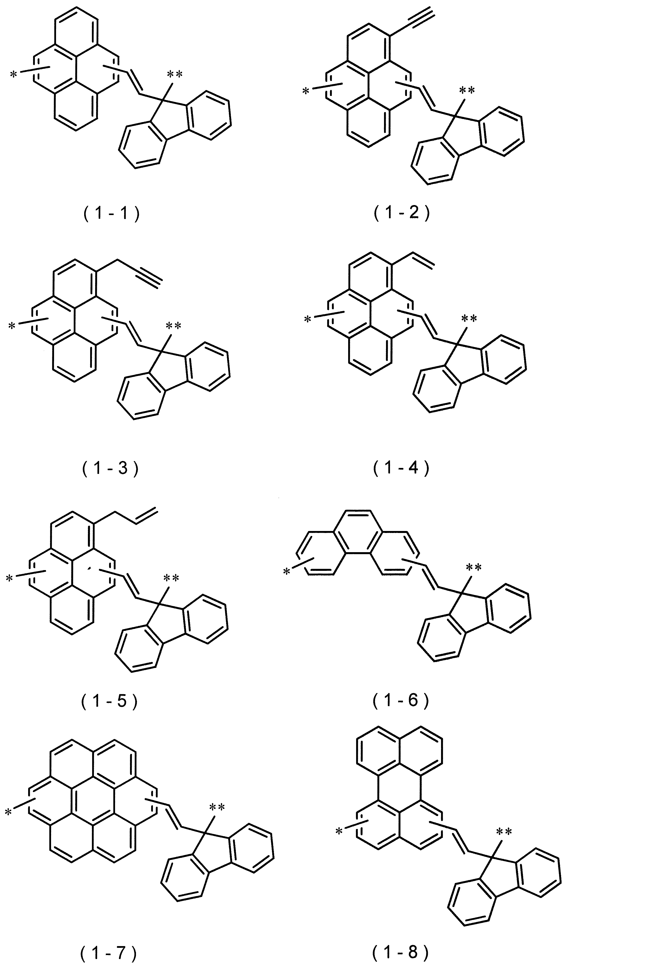
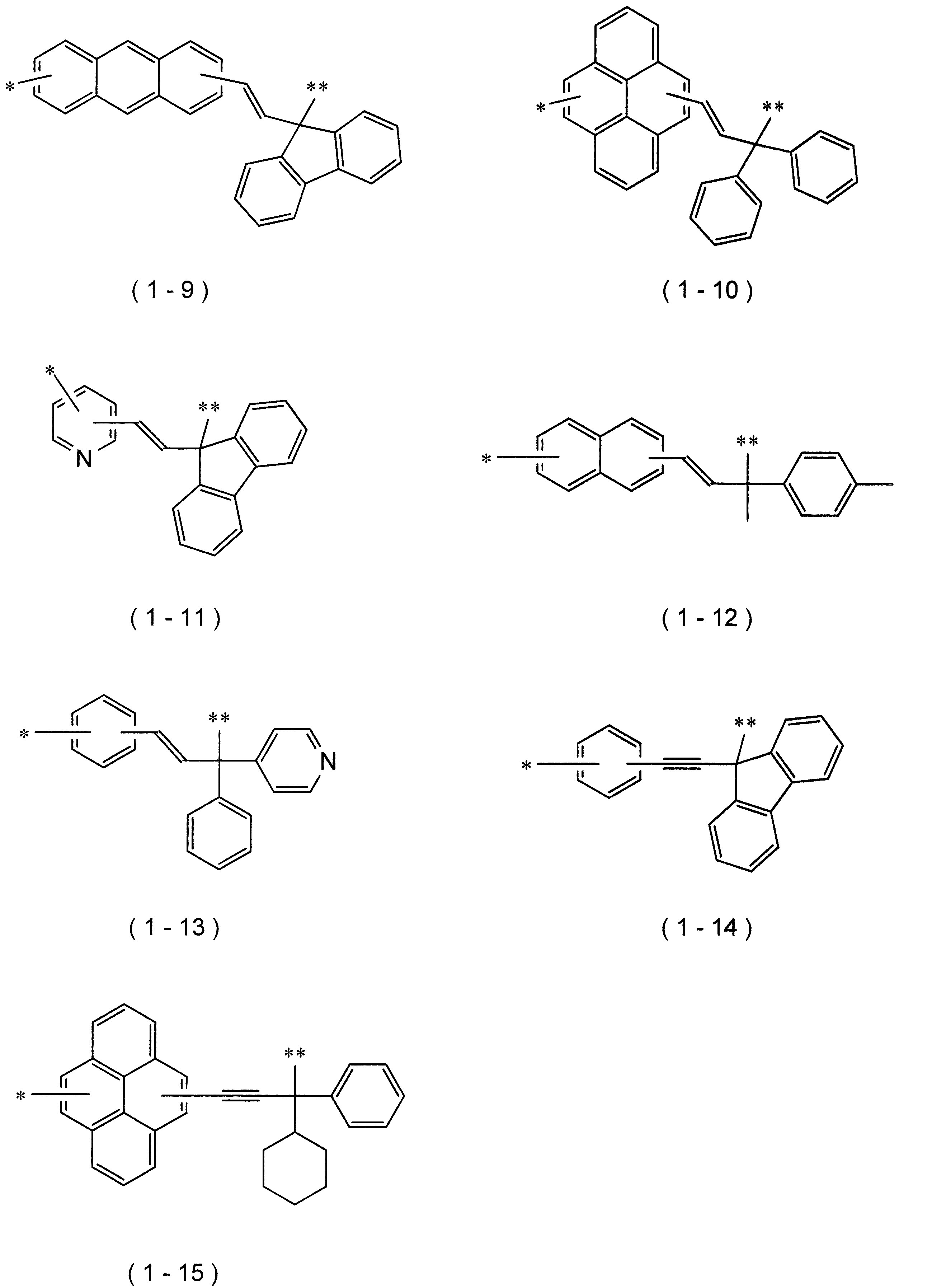
- partial structure (I) examples include structures represented by the following formulas (1-1) to (1-15) (hereinafter, also referred to as “partial structures (I-1) to (I-15)”) and the like. No.
- the partial structures (I-1) to (I-10) are preferable.
- the compound [A] may have one partial structure (I) or a plurality of partial structures (I). [A] The compound may have only one kind of partial structure (I), or may have two or more kinds of partial structures (I). The compound [A] may have another partial structure other than the partial structure (I). Examples of the other partial structure include a partial structure derived from a phenol compound and an aldehyde compound.
- the compound is a compound consisting of only carbon atoms and hydrogen atoms, the etching resistance of the resist underlayer film can be further improved.
- Such an [A] compound has only partial structure (I), and Ar 1 and Ar 2 in the above formula (1) are derived from a hydrocarbon-substituted or unsubstituted arene, and R 2 is a hydrogen atom Or a compound wherein R 3 is an unsubstituted ethenediyl group or an ethenediyl group.
- a polymer having a partial structure in which p in the above formula (1) is 1 as a repeating unit (hereinafter, also referred to as “repeating unit (I)”) may be mentioned. That is, examples of the compound [A] include a polymer having a repeating unit (I) represented by the following formula (i). [A] The compound may have another repeating unit in addition to the repeating unit (I). Examples of the other repeating unit include a repeating unit derived from a phenol compound and an aldehyde compound.
- Ar 11 is a substituted or unsubstituted arenediyl group having 6 to 30 ring members or a substituted or unsubstituted heteroarenediyl group having 5 to 30 ring members.
- Ar 2 , R 2 and R 3 have the same meaning as in the above formula (1).
- Examples of the substituted or unsubstituted arenediyl group having 6 to 30 ring members and the substituted or unsubstituted heteroarenediyl group having 5 to 30 ring members represented by Ar 11 include, for example, the substituted or unsubstituted substituted or unsubstituted groups exemplified as Ar 2 above. Examples include an aryl group having 6 to 30 ring members and a substituted or unsubstituted heteroaryl group having 5 to 30 ring members in which one hydrogen atom on an aromatic carbon ring or an aromatic heterocyclic ring is removed.
- the lower limit of the molecular weight of the compound [A] is preferably 300, more preferably 500, still more preferably 1,000, and particularly preferably 1,500.
- the upper limit of the molecular weight is preferably 100,000, more preferably 50,000, still more preferably 10,000, particularly preferably 8,000, particularly preferably 5,000, and most preferably 3,000.
- the compound [A] can be used alone or in combination of two or more. When there are two or more [A] compounds, the molecular weight of the [A] compound refers to the weight average molecular weight.
- the lower limit of the content of carbon atoms in the compound [A] is preferably 85% by mass, more preferably 90% by mass, still more preferably 93% by mass, and particularly preferably 95% by mass.
- the upper limit of the carbon atom content is, for example, 99.9% by mass, preferably 99% by mass, and more preferably 97% by mass.
- the upper limit of the content of hydrogen atoms in the compound [A] is preferably 7% by mass, more preferably 6% by mass, still more preferably 5% by mass, and particularly preferably 4% by mass.
- the lower limit of the hydrogen atom content is, for example, 0.1% by mass, preferably 1% by mass, and more preferably 2% by mass.
- the upper limit of the oxygen atom content in the compound [A] is preferably 10% by mass, more preferably 5% by mass, still more preferably 2% by mass, and particularly preferably 1% by mass.
- the oxygen atom content may be 0% by mass.
- the etching resistance can be further improved.
- the lower limit of the content of the compound [A] is preferably 50% by mass, more preferably 70% by mass, and still more preferably 85% by mass, based on all components other than the solvent [B] of the composition (I).
- the upper limit of the content is, for example, 100% by mass.
- the lower limit of the content of the compound [A] in the composition (I) is preferably 1% by mass, more preferably 3% by mass, and still more preferably 5% by mass.
- the upper limit of the content is preferably 50% by mass, more preferably 30% by mass, and still more preferably 15% by mass.
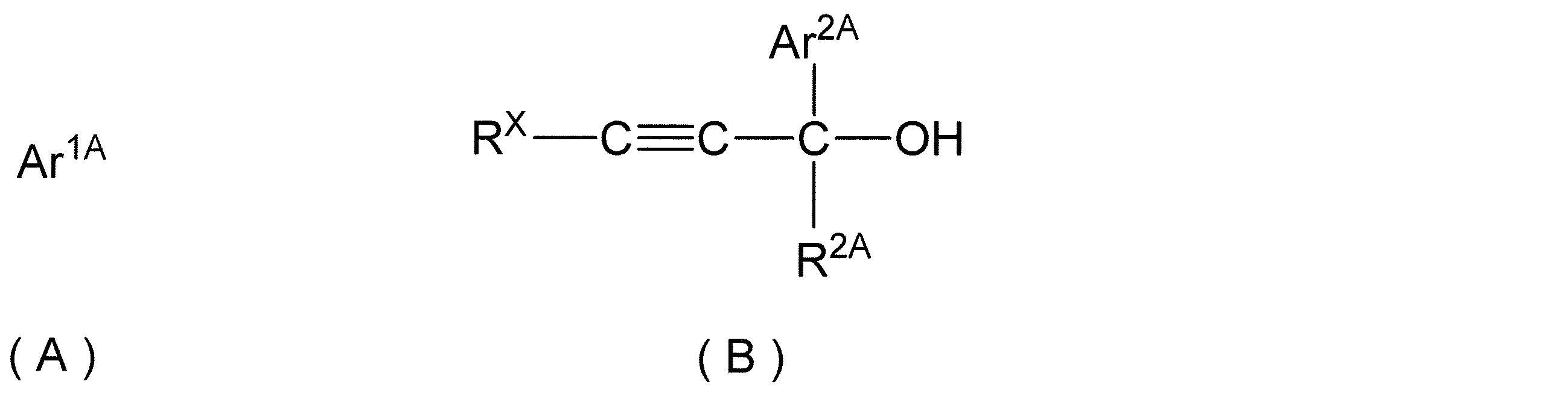
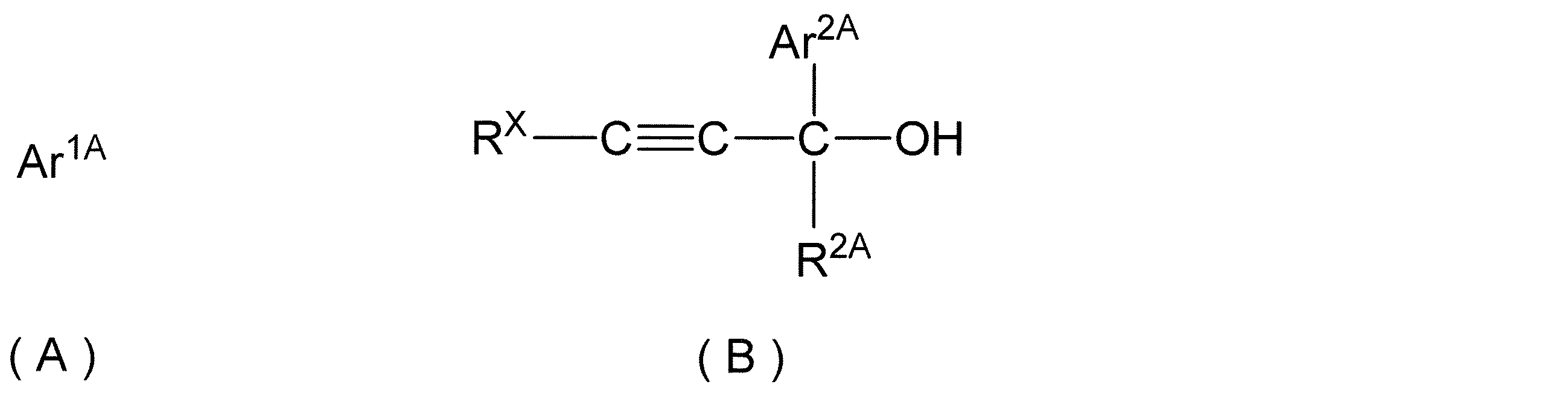
- the compound is, for example, a compound represented by the following formula (A) (hereinafter also referred to as “compound (A)”) and a compound represented by the following formula (B) (hereinafter referred to as “compound (B)”). ) In the presence of an acid catalyst in the presence of an acid catalyst.
- Ar 1A is a substituted or unsubstituted arene having 6 to 30 ring members or a substituted or unsubstituted heteroarene having 5 to 30 ring members.
- Ar 2A is a substituted or unsubstituted aryl group having 6 to 30 ring members or a substituted or unsubstituted heteroaryl group having 5 to 30 ring members, and R 2A is a hydrogen atom or a carbon atom having 1 to 30 ring members.
- a monovalent organic group of up to 20 or Ar 2A and R 2A are one of a ring structure having 3 to 20 ring members in which Ar 2A and R 2A are combined with each other and formed together with a carbon atom to which they are bonded.
- R X is a hydrogen atom or a monovalent organic group having 1 to 20 carbon atoms.
- Examples of the substituted or unsubstituted arene having 6 to 30 ring members and the substituted or unsubstituted heteroarene having 5 to 30 ring members represented by Ar 1A include, for example, the substituted or unsubstituted 6 to 30 ring member providing Ar 1 described above.
- Compounds similar to the compounds exemplified as the arene of 30 and the substituted or unsubstituted heteroarene having 5 to 30 ring members are exemplified.
- Examples of the substituted or unsubstituted aryl group having 6 to 30 ring members and the substituted or unsubstituted heteroaryl group having 5 to 30 ring members represented by Ar 2A include, for example, the substituent exemplified as Ar 2 in the above formula (1). Or an unsubstituted aryl group having 6 to 30 ring members and a group similar to a substituted or unsubstituted heteroaryl group having 5 to 30 ring members.
- Examples of the monovalent organic group having 1 to 20 carbon atoms represented by R 2A include the same groups as the monovalent organic group having 1 to 20 carbon atoms exemplified as R 2 in the above formula (1). Can be
- Examples of the ring structure having 3 to 20 ring members formed by Ar 2A and R 2A include the ring structure having 3 to 20 ring members exemplified as the ring structure formed by Ar 2 and R 2 in the above formula (1). A similar structure is exemplified.
- Examples of the monovalent organic group having 1 to 20 carbon atoms represented by R X include the same groups as the monovalent organic group having 1 to 20 carbon atoms exemplified as R 2 in the above formula (1).
- R X a hydrogen atom is preferable.
- reaction conditions for the condensation reaction conventionally known conditions for the condensation reaction performed in the presence of an acid catalyst can be adopted.
- the acid catalyst may be any of a protonic acid, a Bronsted acid, and a Lewis acid.
- the acid catalyst include inorganic acids such as sulfuric acid, phosphoric acid and perchloric acid, organic sulfonic acids such as p-toluenesulfonic acid, and organic acids such as carboxylic acids such as formic acid, acetic acid and oxalic acid.
- the lower limit of the amount of the acid catalyst used is preferably 0.01 part by mass, more preferably 0.1 part by mass, and preferably 1 part by mass, based on 100 parts by mass of the total of the compound (A) and the compound (B). More preferably, 10 parts by mass is particularly preferred.
- the upper limit of the amount used is preferably 1,000 parts by mass, more preferably 500 parts by mass, further preferably 200 parts by mass, and particularly preferably 100 parts by mass.
- the lower limit of the reaction temperature in the condensation reaction is preferably 40 ° C, more preferably 50 ° C, still more preferably 60 ° C, and particularly preferably 70 ° C.
- 200 ° C is preferred
- 150 ° C is more preferred
- 130 ° C is still more preferred
- 100 ° C is especially preferred.
- the lower limit of the reaction time in the condensation reaction is preferably 5 minutes, more preferably 30 minutes, still more preferably 1 hour, and particularly preferably 2 hours.
- the upper limit of the reaction time is preferably 100 hours, more preferably 50 hours, further preferably 24 hours, and particularly preferably 12 hours.
- reaction solvent used for the condensation reaction include the same solvents as those exemplified as the solvent [B] described below. Of these, ether solvents are preferred, cyclic ether solvents are more preferred, and 1,4-dioxane is even more preferred.
- R X in the above formula (B) is a hydrogen atom
- the above condensation reaction produces a compound [A] in which R 3 in the above formula (1) is an unsubstituted ethenediyl group or an ethyndiyl group.
- the compound [A] can be isolated by appropriately treating the reaction solution of the above condensation reaction by a known method and performing purification such as distillation and recrystallization.
- the solvent is not particularly limited as long as it can dissolve or disperse the [A] compound and optional components contained as necessary.
- Solvents include, for example, alcohol solvents, ketone solvents, ether solvents, ester solvents, and nitrogen-containing solvents.
- the solvent can be used alone or in combination of two or more.
- alcohol-based solvent examples include monoalcohol-based solvents such as methanol, ethanol, and n-propanol, and polyhydric alcohol-based solvents such as ethylene glycol and 1,2-propylene glycol.
- ketone solvents examples include chain ketone solvents such as methyl ethyl ketone and methyl isobutyl ketone, and cyclic ketone solvents such as cyclohexanone.
- ether solvents include chain ether solvents such as n-butyl ether, polyhydric alcohol ether solvents such as cyclic ether solvents such as tetrahydrofuran and 1,4-dioxane, and polyhydric alcohol partial ethers such as diethylene glycol monomethyl ether. System solvents and the like.
- ester solvents examples include carbonate solvents such as diethyl carbonate, monoester solvents such as methyl acetate and ethyl acetate, lactone solvents such as ⁇ -butyrolactone, diethylene glycol monomethyl ether acetate, and propylene glycol monomethyl acetate acetate.
- Examples include a hydric alcohol partial ether carboxylate-based solvent and a lactic acid ester-based solvent such as methyl lactate and ethyl lactate.
- nitrogen-containing solvent examples include a chain nitrogen-containing solvent such as N, N-dimethylacetamide and a cyclic nitrogen-containing solvent such as N-methylpyrrolidone.
- the solvent is preferably a ketone solvent, more preferably a cyclic ketone solvent, and even more preferably cyclohexanone.
- composition (I) may contain an acid generator, a crosslinking agent, a surfactant, an adhesion aid and the like as optional components. These optional components can be used alone or in combination of two or more.
- the acid generator is a component that generates an acid by the action of heat or light and promotes crosslinking of the compound [A].
- the composition (I) contains an acid generator, the cross-linking reaction of the compound [A] is promoted, the hardness of the formed resist underlayer film can be further increased, and the heat resistance of the resist underlayer film can be improved. Can be enhanced.
- Examples of the acid generator include an onium salt compound and an N-sulfonyloxyimide compound.
- the cross-linking agent is a component that forms a cross-linking between components such as the compound [A] in the composition (I) by the action of heat or an acid, or forms a cross-linked structure by itself.
- the composition (I) contains a crosslinking agent, the hardness of the formed resist underlayer film can be increased, and the heat resistance of the resist underlayer film can be further increased.
- crosslinking agent examples include a polyfunctional (meth) acrylate compound, an epoxy compound, a phenol compound substituted with a hydroxymethyl group, a phenol compound containing an alkoxyalkyl group, and a compound having an alkoxyalkylated amino group.
- composition (II) contains [A ′] a condensation reaction product and [B] a solvent.
- the composition (II) may contain optional components as long as the effects of the present invention are not impaired. Hereinafter, each component will be described.
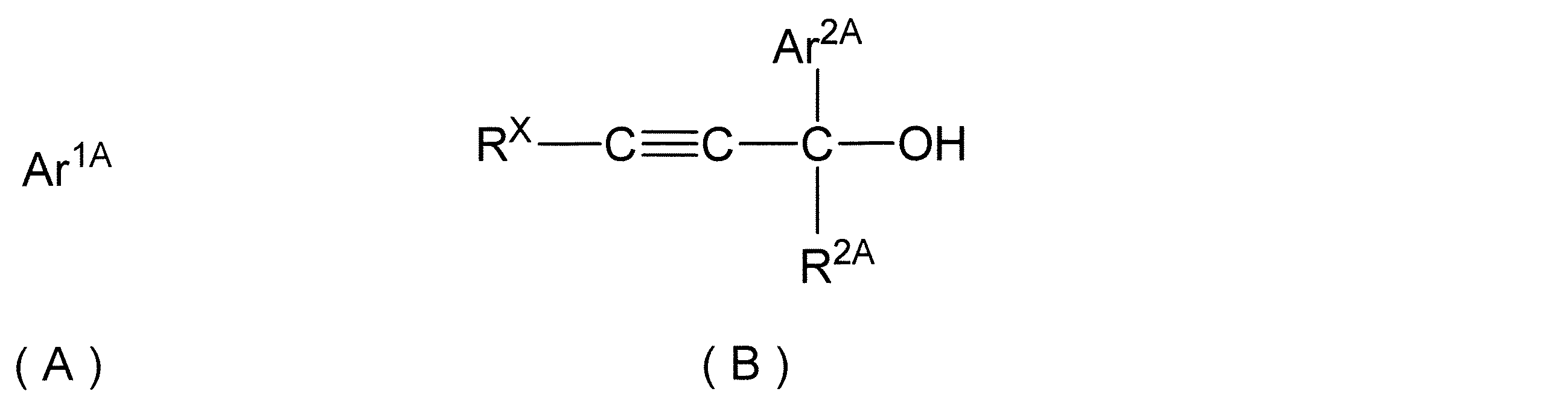
- the condensation reaction product is an acid-catalyzed condensation reaction product of a compound represented by the following formula (A) (compound (A)) and a compound represented by the following formula (B) (compound (B)) It is.
- Ar 1A is a substituted or unsubstituted arene having 6 to 30 ring members or a substituted or unsubstituted heteroarene having 5 to 30 ring members.
- Ar 2A is a substituted or unsubstituted aryl group having 6 to 30 ring members or a substituted or unsubstituted heteroaryl group having 5 to 30 ring members, and R 2A is a hydrogen atom or a carbon atom having 1 to 30 ring members.
- a monovalent organic group of up to 20 or Ar 2A and R 2A are one of a ring structure having 3 to 20 ring members in which Ar 2A and R 2A are combined with each other and formed together with a carbon atom to which they are bonded.
- R X is a hydrogen atom or a monovalent organic group having 1 to 20 carbon atoms.
- the condensation reaction product is a compound having a step of subjecting the compound (A) and the compound (B) to a condensation reaction in the presence of an acid catalyst as described in the above section “[A] Method for producing compound”. Depending on the production method, it can be produced as a product of a condensation reaction.
- the solvent [B] and the optional component in the composition (II) are the same as the solvent [B] and the optional component in the composition (I) described above.
- the composition is obtained by mixing the [A] compound or the [A '] condensation reaction product, the [B] solvent and, if necessary, an optional component at a predetermined ratio, and preferably forming a mixture having a pore diameter of 0.1 ⁇ m or less.
- the lower limit of the solid content concentration of the composition is preferably 0.1% by mass, more preferably 1% by mass, still more preferably 3% by mass, and particularly preferably 5% by mass.
- the upper limit of the solid content concentration is preferably 50% by mass, more preferably 30% by mass, still more preferably 20% by mass, and particularly preferably 15% by mass.
- the solid content concentration was calculated by calcining 0.5 g of the composition for 30 minutes at 250 ° C. and measuring the mass of the solid content with respect to 0.5 g of the composition.
- the resist underlayer film is formed from the composition (composition (I) or composition (II)). Since the resist underlayer film is formed from the above-described composition, it is excellent in etching resistance, heat resistance, flatness, and film defect suppression.
- the method for forming the resist underlayer film includes a step of directly or indirectly applying the composition to a substrate (hereinafter, also referred to as a “coating step”).
- composition is applied directly or indirectly to the substrate.
- the substrate examples include a silicon wafer and a wafer coated with aluminum.
- the method of applying the composition is not particularly limited, and can be performed by an appropriate method such as spin coating, cast coating, roll coating, and the like, whereby a coating film can be formed. it can.
- the coating film may be heated.
- the heating of the coating film is usually performed in the air, but may be performed in a nitrogen atmosphere.
- the lower limit of the heating temperature is preferably 200 ° C., more preferably 250 ° C., and even more preferably 300 ° C.
- the upper limit of the temperature is preferably 600 ° C., more preferably 500 ° C., and even more preferably 400 ° C.
- the lower limit of the heating time is preferably 15 seconds, and more preferably 30 seconds. As an upper limit of the above-mentioned time, 1,200 seconds are preferred and 600 seconds are more preferred.
- the coating film Before the coating film is heated, it may be preheated at a temperature of 60 ° C or more and 150 ° C or less. As a minimum of time in preheating, 10 seconds are preferred and 30 seconds are more preferred. As an upper limit of the above-mentioned time, 300 seconds are preferred and 180 seconds are more preferred.
- a resist underlayer film can be formed.
- the coating film is heated to form a film.
- the composition contains an acid generator and the acid generator is a radiation-sensitive acid generator.
- the resist underlayer film can be formed by curing the coating film by combining exposure and heating.
- the radiation used for this exposure is appropriately selected from electromagnetic waves such as visible light, ultraviolet light, far ultraviolet light, X-rays and ⁇ -rays, electron beams, molecular beams, and particle beams such as ion beams, depending on the type of the acid generator. Is done.
- the lower limit of the average thickness of the formed resist underlayer film is preferably 30 nm, more preferably 50 nm, and even more preferably 100 nm.
- the upper limit of the average thickness is preferably 3,000 nm, more preferably 2,000 nm, and even more preferably 500 nm.
- the pattern forming method includes a step of directly or indirectly applying the composition to a substrate (hereinafter, also referred to as a “resist underlayer film forming composition coating step”) and the resist underlayer film forming composition coating step.
- a step of directly or indirectly applying a composition for forming a resist film to a resist underlayer film formed by the step (hereinafter, also referred to as a “step of applying a composition for forming a resist film”), and the composition for forming a resist film
- the method includes a step of exposing the resist film formed by the coating step to radiation (hereinafter, also referred to as an “exposure step”), and a step of developing the exposed resist film (hereinafter, also referred to as a “development step”). .
- the pattern forming method may further include, after the developing step, a step of performing etching using the resist pattern formed by the developing step as a mask (hereinafter, also referred to as an “etching step”).
- the pattern forming method since the resist underlayer film having excellent etching resistance, heat resistance, flatness, and film defect suppressing property described above is used, a pattern having a good shape can be obtained.
- the pattern forming method if necessary, before the resist film forming composition coating step, directly or indirectly silicon-containing film on the resist underlayer film formed by the resist underlayer film forming composition coating step (Hereinafter, also referred to as “silicon-containing film forming step”). Hereinafter, each step will be described.
- composition for forming resist underlayer film [Coating process of composition for forming resist underlayer film]
- the composition is applied directly or indirectly to the substrate. Thereby, a resist underlayer film is formed.
- This step is the same as the above-described coating step in the method for forming a resist underlayer film.
- Silicon-containing film forming step In this step, a silicon-containing film is formed directly or indirectly on the resist underlayer film formed in the resist underlayer film forming composition coating step.
- the silicon-containing film is formed by directly or indirectly applying the composition for forming a silicon-containing film to the resist underlayer film, and curing the coating film by, for example, exposure and / or heating. You.
- a commercially available product of the composition for forming a silicon-containing film for example, "NFC @ SOG01”, “NFC @ SOG04", “NFC @ SOG080", etc. of JSR Corporation can be used.
- Examples of the radiation used for the exposure include visible light, ultraviolet light, far ultraviolet light, electromagnetic waves such as X-rays and ⁇ -rays, electron beams, molecular beams, and particle beams such as ion beams.
- the lower limit of the temperature at which the coating film is heated is preferably 90 ° C, more preferably 150 ° C, and even more preferably 180 ° C.
- As an upper limit of the above-mentioned temperature 550 ° C is preferred, 450 ° C is more preferred, and 300 ° C is still more preferred.
- the lower limit of the average thickness of the formed silicon-containing film is preferably 1 nm, more preferably 10 nm, and still more preferably 20 nm.
- the upper limit is preferably 20,000 nm, more preferably 1,000 nm, and even more preferably 100 nm.
- a silicon-containing film is formed. It is preferable that the obtained silicon-containing film is further heated (fired) at a temperature of, for example, 350 ° C. or more and 550 ° C. or less for 5 seconds or more and 600 seconds or less.
- resist film forming composition coating process In this step, the resist underlayer film forming composition is applied directly or indirectly to the resist underlayer film formed in the above resist underlayer film forming composition applying step.
- the composition for forming a resist film is applied directly or indirectly to the silicon-containing film.
- this step specifically, after coating the composition for forming a resist film so that the obtained resist film has a predetermined thickness, by pre-baking to evaporate the solvent in the coating film, the resist film To form
- the resist film-forming composition examples include, for example, a positive or negative chemically amplified resist composition containing a radiation-sensitive acid generator, and a positive resist composition containing an alkali-soluble resin and a quinonediazide-based photosensitizer. And a negative resist composition containing an alkali-soluble resin and a crosslinking agent.
- the lower limit of the solid content concentration of the composition for forming a resist film is preferably 0.3% by mass, more preferably 1% by mass.
- the upper limit of the solid content concentration is preferably 50% by mass, and more preferably 30% by mass.
- the composition for forming a resist film is generally filtered, for example, with a filter having a pore size of 0.2 ⁇ m or less, and used for forming a resist film. In this step, a commercially available resist composition can be used as it is.
- the method for applying the composition for forming a resist film is not particularly limited, and examples thereof include a spin coating method.
- the prebaking temperature is appropriately adjusted according to the type of the resist composition used, etc., but the lower limit of the temperature is preferably 30 ° C, more preferably 50 ° C.
- the upper limit of the temperature is preferably 200 ° C, more preferably 150 ° C.
- the lower limit of the pre-bake time is preferably 10 seconds, and more preferably 30 seconds. As an upper limit of the above-mentioned time, 600 seconds are preferred and 300 seconds are more preferred.
- the radiation used for the exposure depending on the type of radiation-sensitive acid generator used in the resist film forming composition, visible light, ultraviolet light, far ultraviolet light, X-rays, electromagnetic waves such as ⁇ -rays, electron beams, It is appropriately selected from particle beams such as a molecular beam and an ion beam.
- KrF excimer laser light (248 nm), ArF excimer laser light (193 nm), F 2 excimer laser light (wavelength 157 nm), Kr 2 excimer laser light (wavelength 147 nm), ArKr excimer laser light (Wavelength 134 nm) or extreme ultraviolet light (wavelength 13.5 nm or the like, EUV) is more preferable, and KrF excimer laser light, ArF excimer laser light or EUV is further preferable.
- post baking can be performed to improve the resolution, pattern profile, developability, and the like.
- the temperature of the post-baking is appropriately adjusted according to the type of the resist composition used, etc., and the lower limit of the temperature is preferably 50 ° C., more preferably 70 ° C.
- the upper limit of the temperature is preferably 200 ° C, more preferably 150 ° C.
- the lower limit of the post-baking time is preferably 10 seconds, and more preferably 30 seconds. As an upper limit of the above-mentioned time, 600 seconds are preferred and 300 seconds are more preferred.
- the exposed resist film is developed.
- This development may be an alkali development or an organic solvent development.
- the developing solution include, in the case of alkali development, for example, sodium hydroxide, potassium hydroxide, sodium carbonate, sodium silicate, sodium metasilicate, ammonia, ethylamine, n-propylamine, diethylamine, di-n-propylamine, triethylamine, methyl Diethylamine, dimethylethanolamine, triethanolamine, tetramethylammonium hydroxide (TMAH), tetraethylammonium hydroxide, pyrrole, piperidine, choline, 1,8-diazabicyclo [5.4.0] -7-undecene, 1,5 And basic aqueous solutions such as -diazabicyclo [4.3.0] -5-nonene.
- TMAH tetramethylammonium hydroxide
- a water-soluble organic solvent such as an alcohol such as methanol or ethanol, a surfactant, or the like
- examples of the developer include various organic solvents exemplified as the solvent [B] of the above-described composition.
- etching is performed using the resist pattern formed in the developing step as a mask. Thereby, a pattern is formed on the substrate.
- the number of times of etching may be one or more, that is, etching may be sequentially performed using a pattern obtained by etching as a mask, but a plurality of times is preferable from the viewpoint of obtaining a pattern having a better shape.
- etching is sequentially performed in the order of the silicon-containing film, the resist underlayer film, and the substrate.
- the etching method include dry etching and wet etching. Among these, dry etching is preferable from the viewpoint of improving the shape of the pattern of the substrate. For this dry etching, for example, gas plasma such as oxygen plasma or the like is used. After the above etching, a patterned substrate having a predetermined pattern is obtained.
- the average molecular weight (weight-average molecular weight (Mw)) of the compound was measured using a GPC column (2 columns of “G2000HXL” and 1 column of “G3000HXL”) manufactured by Tosoh Corporation at a flow rate of 1.0 mL / min and an elution solvent of tetrahydrofuran.
- Column temperature Measured by gel permeation chromatography (detector: differential refractometer) using monodisperse polystyrene as a standard under the analysis conditions of 40 ° C.
- Example 1-1 Under a nitrogen atmosphere, 20.0 g of pyrene, 37.6 g of p-toluenesulfonic acid monohydrate, 40.8 g of 9-ethynyl-9-fluorenol and 220.36 g of 1,4-dioxane were added to the reaction vessel.
- the compound (A-1) was obtained by reacting at a temperature of 3 ° C. for 3 hours.
- the weight average molecular weight (Mw) of the obtained compound (A-1) was 2,800.
- Example 1-2 Compound (A-2) was obtained in the same manner as in Example 1-1.
- the weight average molecular weight (Mw) of the obtained compound (A-2) was 2,500.
- Example 1-3 Compound (A-3) was obtained in the same manner as in Example 1-1.
- the weight average molecular weight (Mw) of the obtained compound (A-3) was 2,400.
- Example 1-4 Compound (A-4) was obtained in the same manner as in Example 1-1.
- the weight average molecular weight (Mw) of the obtained compound (A-4) was 2,300.
- Example 1-5 In the same manner as in Example 1-1, the above compound (A-5) was obtained.
- the weight average molecular weight (Mw) of the obtained compound (A-5) was 2,400.
- Example 1-6 Compound (A-6) was obtained in the same manner as in Example 1-1.
- the weight average molecular weight (Mw) of the obtained compound (A-6) was 2,100.
- Example 1-7 Compound (A-7) was obtained in the same manner as in Example 1-1.
- the weight average molecular weight (Mw) of the obtained compound (A-7) was 1,800.
- Example 1-8 In the same manner as in Example 1-1, the above compound (A-8) was obtained.
- the weight average molecular weight (Mw) of the obtained compound (A-8) was 2,000.
- Example 1-9 In the same manner as in Example 1-1, the above compound (A-9) was obtained.
- the weight average molecular weight (Mw) of the obtained compound (A-9) was 2,200.
- Example 1-10 Compound (A-10) was obtained in the same manner as in Example 1-1.
- the weight average molecular weight (Mw) of the obtained compound (A-10) was 1,500.
- composition for forming resist underlayer film ⁇ Preparation of composition for forming resist underlayer film>
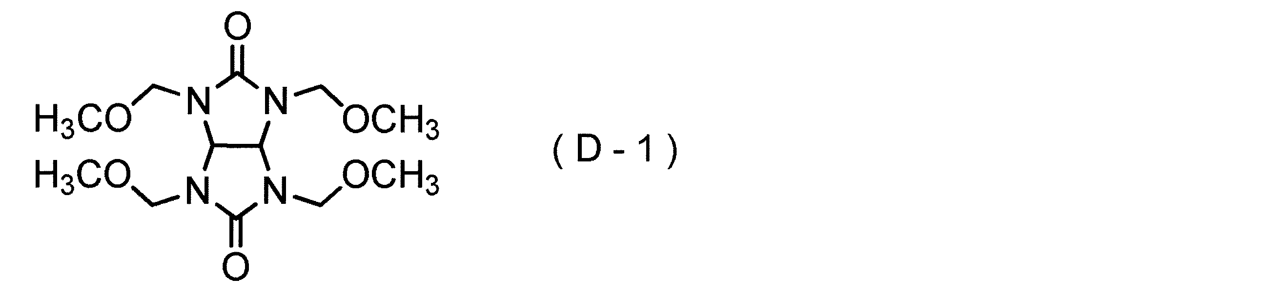
- the compound [A], the solvent [B], the acid generator [C] and the crosslinking agent [D] used in the preparation of the composition for forming a resist underlayer film are shown below.
- Example 2-1 10 parts by mass of (A-1) as a compound [A] was dissolved in 90 parts by mass of (B-1) as a solvent [B]. The resulting solution was filtered through a membrane filter having a pore size of 0.1 ⁇ m to prepare a resist underlayer film forming composition (J-1).
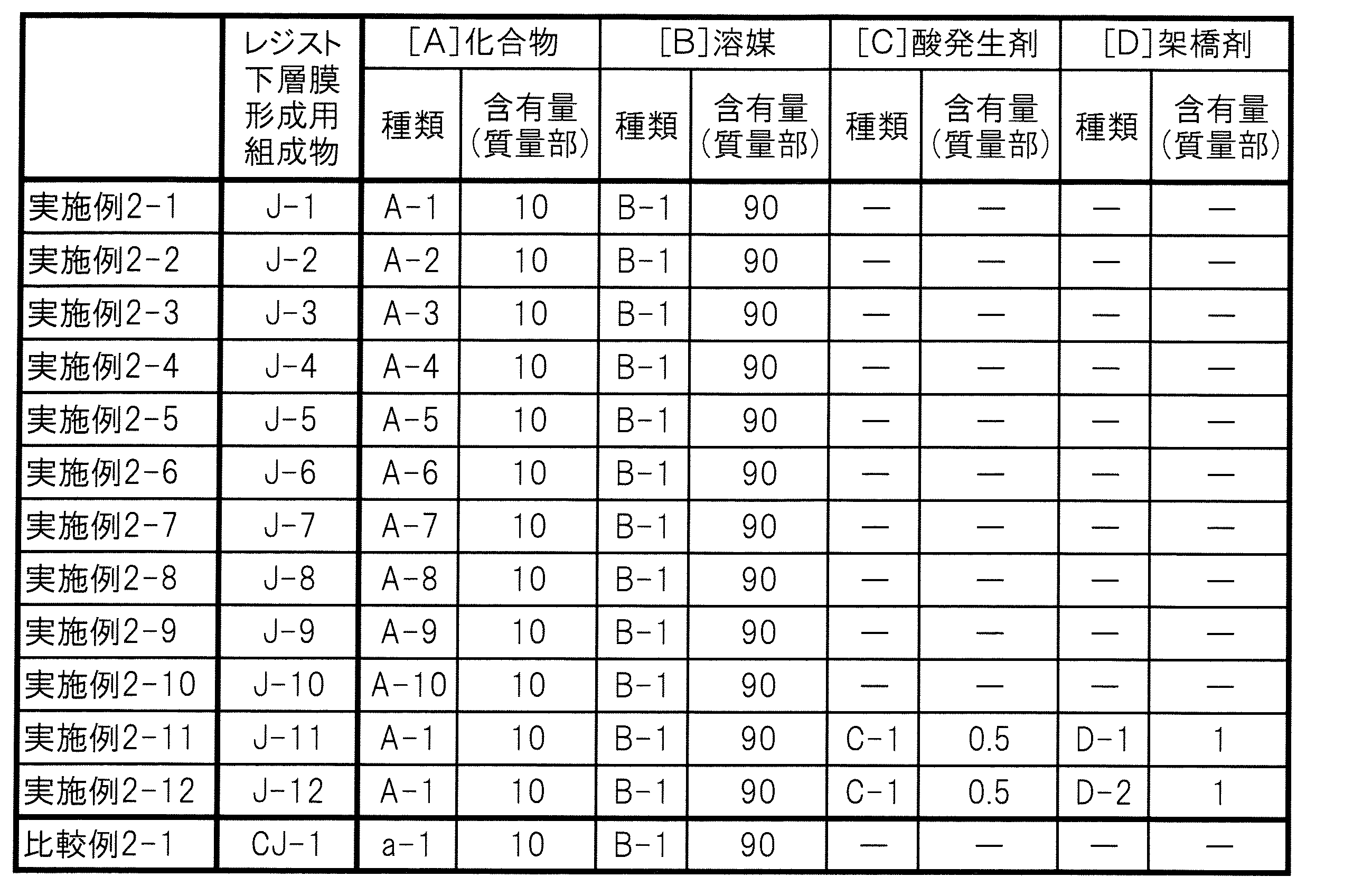
- Example 2-2 to 2-12 and Comparative Example 2-1 Except that the components and contents shown in Table 1 below were used, the same procedures as in Example 2-1 were carried out to obtain the resist underlayer film forming compositions (J-2) to (J-12) and (CJ). -1) was prepared. "-" In Table 1 indicates that the corresponding component was not used.
- M L ⁇ (m1-m2) / m1 ⁇ ⁇ 100
- M L is a mass reduction rate (%)
- m1 is the pre-heating the mass (mg)
- m @ 2 is the mass (mg) at 400 ° C..
- the lower the mass reduction rate of the sample powder the smaller the amount of sublimates and decomposition products of the resist underlayer film generated when the resist underlayer film is heated. That is, the smaller the mass reduction rate, the higher the heat resistance.
- the heat resistance is “A” (extremely good) when the mass loss rate is less than 5%, “B” (good) when it is 5% or more and less than 10%, and “C” (good) when it is 10% or more. Poor).
- the prepared composition for forming a resist underlayer film was coated on a silicon substrate 1 on which a trench pattern having a depth of 100 nm and a width of 10 ⁇ m was formed by a spin coater (“CLEAN TRACK” manufactured by Tokyo Electron Limited). ACT12 ”) by a spin coating method.
- the rotation speed of the spin coating was the same as that in the case of forming a film having an average thickness of 200 nm in the above “Formation of Resist Underlayer Film”.
- the film is heated (fired) at a heating temperature (° C.) and a heating time (sec) shown in Table 2 below in the atmosphere to form a film 2 having an average thickness of 200 nm in the non-trench pattern portion.
- a heating temperature ° C.
- a heating time sec
- the cross-sectional shape of the silicon substrate with the film was observed with a scanning electron microscope (“S-4800” manufactured by Hitachi High-Technologies Corporation), and the height of the film at the central portion b of the trench pattern and the height of the trench pattern were measured.
- the difference ( ⁇ FT) from the height of the non-trench pattern portion “a” at a position 5 ⁇ m from the end was used as an index of flatness.
- the flatness was evaluated as “A” (good) when the ⁇ FT was less than 40 nm, “B” (somewhat good) when it was 40 nm or more and less than 60 nm, and “C” (bad) when it was 60 nm or more. .
- the height difference shown in FIG. 1 is exaggerated from the actual height.
- the composition for forming a silicon-containing film (“NFC SOG080” of JSR Corporation) is applied on the obtained substrate with a resist underlayer film by a spin coating method, and then is applied at 200 ° C. for 60 seconds in an air atmosphere. It was heated (fired) to form a silicon-containing film having an average thickness of 50 nm, and a substrate with a silicon-containing film was obtained. After the obtained substrate with a silicon-containing film was further heated (fired) at 450 ° C. for 60 seconds, the surface of the silicon-containing film was observed with an optical microscope. The film defect suppressing property was evaluated as “A” (good) when no cracking or peeling of the silicon-containing film was observed, and evaluated as “B” (poor) when cracking or peeling of the silicon-containing film was observed. .
- the resist underlayer film formed from the composition for forming a resist underlayer film of the example is excellent in etching resistance, heat resistance, flatness, and film defect suppression.
- the resist underlayer film formed from the composition for forming a resist underlayer film of the comparative example was poor in all of heat resistance, flatness and film defect suppressing properties, and was inferior in etching resistance.
- a resist underlayer film excellent in etching resistance, heat resistance, flatness, and film defect suppressing property can be formed.
- the resist underlayer film of the present invention is excellent in etching resistance, heat resistance, flatness and film defect suppression.
- the method for forming a resist underlayer film of the present invention it is possible to form a resist underlayer film having excellent etching resistance, heat resistance, flatness, and film defect suppression.
- the pattern forming method of the present invention a pattern having a good shape can be obtained by using such an excellent resist underlayer film.
- the compound of the present invention can be suitably used as a component of the composition for forming a resist underlayer film.
- the method for producing a compound of the present invention the compound can be produced. Therefore, they can be suitably used for the manufacture of semiconductor devices, which are expected to be further miniaturized in the future.
Landscapes
- Physics & Mathematics (AREA)
- General Physics & Mathematics (AREA)
- Engineering & Computer Science (AREA)
- Architecture (AREA)
- Structural Engineering (AREA)
- Chemical & Material Sciences (AREA)
- Health & Medical Sciences (AREA)
- Chemical Kinetics & Catalysis (AREA)
- Medicinal Chemistry (AREA)
- Polymers & Plastics (AREA)
- Organic Chemistry (AREA)
- Materials For Photolithography (AREA)
- Exposure And Positioning Against Photoresist Photosensitive Materials (AREA)
- Polyethers (AREA)
- Organic Low-Molecular-Weight Compounds And Preparation Thereof (AREA)
Abstract
Description


式(B)中、Ar2Aは置換若しくは非置換の環員数6~30のアリール基若しくは置換若しくは非置換の環員数5~30のヘテロアリール基であり、R2Aは水素原子若しくは炭素数1~20の1価の有機基であるか、又はAr2A及びR2Aは、Ar2AとR2Aとが互いに合わせられこれらが結合する炭素原子と共に構成される環員数3~20の環構造の一部である。RXは、水素原子又は炭素数1~20の1価の有機基である。)
当該レジスト下層膜形成用組成物(以下、単に「組成物」ともいう)の態様としては、以下に示す組成物(I)及び組成物(II)が挙げられる。
組成物(I):[A]化合物と[B]溶媒とを含有する
組成物(II):[A’]縮合反応生成物と[B]溶媒とを含有する
以下、組成物(I)、組成物(II)の順に説明する。
組成物(I)は、[A]化合物と[B]溶媒とを含有する。組成物(I)は、本発明の効果を損なわない範囲において、任意成分を含有していてもよい。
以下、各成分について説明する。
[A]化合物は、部分構造(I)を有する化合物である。部分構造(I)は、下記式(1)で表される。


[A]化合物は、例えば下記式(A)で表される化合物(以下、「化合物(A)」ともいう)と下記式(B)で表される化合物(以下、「化合物(B)」ともいう)とを酸触媒の存在下で、縮合反応させる工程を備える化合物の製造方法等により製造することができる。

上記式(B)中、Ar2Aは置換若しくは非置換の環員数6~30のアリール基若しくは置換若しくは非置換の環員数5~30のヘテロアリール基であり、R2Aは水素原子若しくは炭素数1~20の1価の有機基であるか、又はAr2A及びR2Aは、Ar2AとR2Aとが互いに合わせられこれらが結合する炭素原子と共に構成される環員数3~20の環構造の一部である。RXは、水素原子又は炭素数1~20の1価の有機基である。
RXとしては、水素原子が好ましい。
[B]溶媒は、[A]化合物及び必要に応じて含有する任意成分を溶解又は分散することができれば特に限定されない。
組成物(I)は、任意成分として、酸発生剤、架橋剤、界面活性剤、密着助剤等を含有してもよい。これらの任意成分は、1種単独で又は2種以上を組み合わせて用いることができる。
酸発生剤は、熱や光の作用により酸を発生し、[A]化合物の架橋を促進する成分である。組成物(I)が酸発生剤を含有することで[A]化合物の架橋反応が促進され、形成されるレジスト下層膜の硬度をより高めることができ、また、レジスト下層膜の耐熱性をより高めることができる。
架橋剤は、熱や酸の作用により、組成物(I)中の[A]化合物等の成分同士の架橋結合を形成するか、又は自らが架橋構造を形成する成分である。組成物(I)が架橋剤を含有する場合、形成されるレジスト下層膜の硬度を高めることができ、また、レジスト下層膜の耐熱性をより高めることができる。
組成物(II)は、[A’]縮合反応生成物と、[B]溶媒とを含有する。組成物(II)は、本発明の効果を損なわない範囲において、任意成分を含有していてもよい。
以下、各成分について説明する。
[A’]縮合反応生成物は、下記式(A)で表される化合物(化合物(A))及び下記式(B)で表される化合物(化合物(B))の酸触媒縮合反応生成物である。
上記式(B)中、Ar2Aは置換若しくは非置換の環員数6~30のアリール基若しくは置換若しくは非置換の環員数5~30のヘテロアリール基であり、R2Aは水素原子若しくは炭素数1~20の1価の有機基であるか、又はAr2A及びR2Aは、Ar2AとR2Aとが互いに合わせられこれらが結合する炭素原子と共に構成される環員数3~20の環構造の一部である。RXは、水素原子又は炭素数1~20の1価の有機基である。
当該組成物は、[A]化合物又は[A’]縮合反応生成物、[B]溶媒及び必要に応じて任意成分を所定の割合で混合し、好ましくは得られた混合物を孔径0.1μm以下のメンブランフィルター等で濾過することにより調製することができる。当該組成物の固形分濃度の下限としては、0.1質量%が好ましく、1質量%がより好ましく、3質量%がさらに好ましく、5質量%が特に好ましい。上記固形分濃度の上限としては、50質量%が好ましく、30質量%がより好ましく、20質量%がさらに好ましく、15質量%が特に好ましい。上記固形分濃度は、当該組成物0.5gを30分間250℃で焼成することで、当該組成物0.5gに対する固形分の質量を測定することにより算出した。
当該レジスト下層膜は、当該組成物(組成物(I)又は組成物(II))から形成される。当該レジスト下層膜は、上述の当該組成物から形成されるので、エッチング耐性、耐熱性、平坦性及び膜欠陥抑制性に優れている。
当該レジスト下層膜の形成方法は、基板に直接又は間接に当該組成物を塗工する工程(以下、「塗工工程」ともいう)を備える。
本工程では、基板に直接又は間接に当該組成物を塗工する。
当該パターン形成方法は、基板に直接又は間接に当該組成物を塗工する工程(以下、「レジスト下層膜形成用組成物塗工工程」ともいう)と、上記レジスト下層膜形成用組成物塗工工程により形成されたレジスト下層膜に直接又は間接にレジスト膜形成用組成物を塗工する工程(以下、「レジスト膜形成用組成物塗工工程」ともいう)と、上記レジスト膜形成用組成物塗工工程により形成されたレジスト膜を放射線により露光する工程(以下、「露光工程」ともいう)と、上記露光されたレジスト膜を現像する工程(以下、「現像工程」ともいう)とを備える。
本工程では、基板に直接又は間接に当該組成物を塗工する。これによりレジスト下層膜が形成される。本工程は、上述の当該レジスト下層膜の形成方法における塗工工程と同様である。
本工程では、上記レジスト下層膜形成用組成物塗工工程により形成されたレジスト下層膜に直接又は間接にケイ素含有膜を形成する。
本工程では、上記レジスト下層膜形成用組成物塗工工程により形成されたレジスト下層膜に直接又は間接にレジスト膜形成用組成物を塗工する。上記ケイ素含有膜形成工程を行った場合には、上記レジスト膜形成用組成物を上記ケイ素含有膜に直接又は間接に塗工する。
本工程では、上記レジスト膜形成用組成物塗工工程により形成されたレジスト膜を放射線により露光する。
本工程では、上記露光されたレジスト膜を現像する。この現像は、アルカリ現像であっても有機溶媒現像であってもよい。現像液としては、アルカリ現像の場合、例えば水酸化ナトリウム、水酸化カリウム、炭酸ナトリウム、珪酸ナトリウム、メタ珪酸ナトリウム、アンモニア、エチルアミン、n-プロピルアミン、ジエチルアミン、ジ-n-プロピルアミン、トリエチルアミン、メチルジエチルアミン、ジメチルエタノールアミン、トリエタノールアミン、テトラメチルアンモニウムヒドロキシド(TMAH)、テトラエチルアンモニウムヒドロキシド、ピロール、ピペリジン、コリン、1,8-ジアザビシクロ[5.4.0]-7-ウンデセン、1,5-ジアザビシクロ[4.3.0]-5-ノネン等の塩基性水溶液が挙げられる。これらの塩基性水溶液には、例えばメタノール、エタノール等のアルコール類などの水溶性有機溶媒、界面活性剤等を適量添加することもできる。また、有機溶媒現像の場合、現像液としては、例えば上述の組成物の[B]溶媒として例示した種々の有機溶媒等が挙げられる。
本工程では、上記現像工程により形成されたレジストパターンをマスクとしたエッチングを行う。これにより、基板にパターンが形成される。エッチングの回数としては1回でも、複数回、すなわちエッチングにより得られるパターンをマスクとして順次エッチングを行ってもよいが、より良好な形状のパターンを得る観点からは、複数回が好ましい。複数回のエッチングを行う場合、ケイ素含有膜、レジスト下層膜、基板の順に順次エッチングを行う。エッチングの方法としては、ドライエッチング、ウエットエッチング等が挙げられる。これらの中で、基板のパターンの形状をより良好なものとする観点から、ドライエッチングが好ましい。このドライエッチングには、例えば酸素プラズマ等のガスプラズマ等が用いられる。上記エッチングの後、所定のパターンを有するパターニングされた基板が得られる。
化合物の平均分子量(重量平均分子量(Mw))は、東ソー(株)のGPCカラム(「G2000HXL」2本及び「G3000HXL」1本)を用い、流量:1.0mL/分、溶出溶媒:テトラヒドロフラン、カラム温度:40℃の分析条件で、単分散ポリスチレンを標準とするゲルパーミエーションクロマトグラフィー(検出器:示差屈折計)により測定した。
レジスト下層膜の平均厚みは、分光エリプソメータ(J.A.WOOLLAM社の「M2000D」)を用いて測定した。
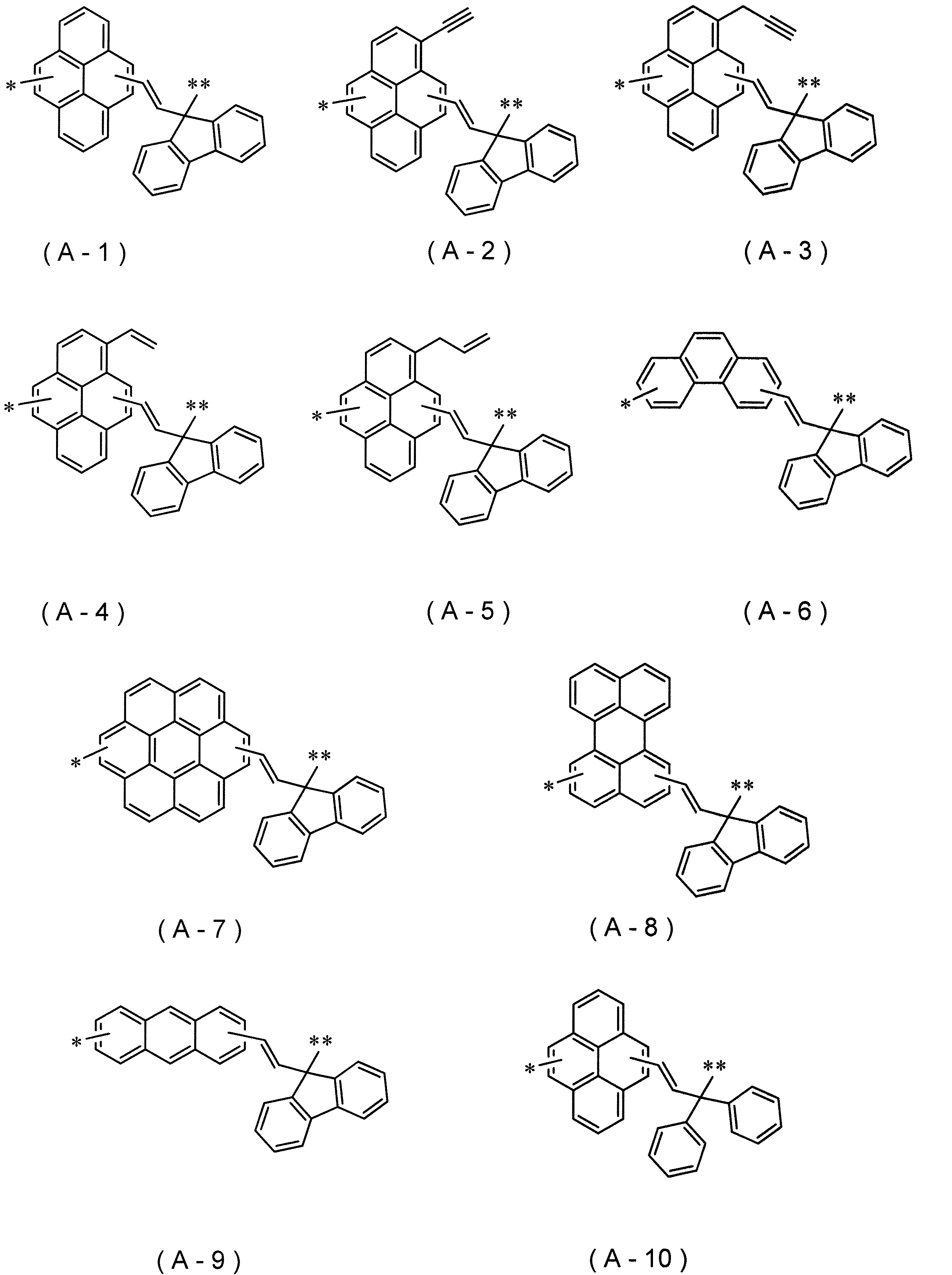
[A]化合物としての下記式(A-1)~(A-10)で表される部分構造を繰り返し単位として有する重合体(以下、「化合物(A-1)~(A-10)」ともいう)を、以下に示す手順により合成した。
反応容器に、窒素雰囲気下、ピレン20.0g、p-トルエンスルホン酸・一水和物37.6g、9-エチニル-9-フルオレノール40.8g及び1,4-ジオキサン220.36gを加え、80℃で3時間反応させることで、上記化合物(A-1)を得た。得られた化合物(A-1)の重量平均分子量(Mw)は、2,800であった。
実施例1-1と同様にして、上記化合物(A-2)を得た。得られた化合物(A-2)の重量平均分子量(Mw)は、2,500であった。
実施例1-1と同様にして、上記化合物(A-3)を得た。得られた化合物(A-3)の重量平均分子量(Mw)は、2,400であった。
実施例1-1と同様にして、上記化合物(A-4)を得た。得られた化合物(A-4)の重量平均分子量(Mw)は、2,300であった。
実施例1-1と同様にして、上記化合物(A-5)を得た。得られた化合物(A-5)の重量平均分子量(Mw)は、2,400であった。
実施例1-1と同様にして、上記化合物(A-6)を得た。得られた化合物(A-6)の重量平均分子量(Mw)は、2,100であった。
実施例1-1と同様にして、上記化合物(A-7)を得た。得られた化合物(A-7)の重量平均分子量(Mw)は、1,800であった。
実施例1-1と同様にして、上記化合物(A-8)を得た。得られた化合物(A-8)の重量平均分子量(Mw)は、2,000であった。
実施例1-1と同様にして、上記化合物(A-9)を得た。得られた化合物(A-9)の重量平均分子量(Mw)は、2,200であった。
実施例1-1と同様にして、上記化合物(A-10)を得た。得られた化合物(A-10)の重量平均分子量(Mw)は、1,500であった。
反応容器に、窒素雰囲気下、p-クレゾール250.0g、37質量%ホルマリン125.0g及び無水シュウ酸2gを加え、100℃で3時間、さらに180℃で1時間反応させた後、減圧下にて未反応モノマーを除去し、下記式(a-1)で表される樹脂を得た。得られた樹脂(a-1)の重量平均分子量(Mw)は、11,000であった。

レジスト下層膜形成用組成物の調製に用いた[A]化合物、[B]溶媒、[C]酸発生剤及び[D]架橋剤について以下に示す。
実施例:上記合成した化合物(A-1)~(A-10)
比較例:上記合成した樹脂(a-1)
B-1:シクロヘキサノン
C-1:ビス(4-t-ブチルフェニル)ヨードニウムノナフルオロ-n-ブタンスルホネート(下記式(C-1)で表される化合物)

D-1:1,3,4,6-テトラキス(メトキシメチル)グリコールウリル(下記式(D-1)で表される化合物)
[A]化合物としての(A-1)10質量部を[B]溶媒としての(B-1)90質量部に溶解した。得られた溶液を孔径0.1μmのメンブランフィルターで濾過して、レジスト下層膜形成用組成物(J-1)を調製した。
下記表1に示す種類及び含有量の各成分を使用した以外は実施例2-1と同様に操作して、レジスト下層膜形成用組成物(J-2)~(J-12)及び(CJ-1)を調製した。表1中の「-」は、該当する成分を使用しなかったことを示す。
[実施例3-1~3-12及び比較例3-1]
上記調製したレジスト下層膜形成用組成物を、シリコンウエハ(基板)上に、スピンコーター(東京エレクトロン(株)の「CLEAN TRACK ACT12」)を用い、回転塗工法により塗工した。次に、大気雰囲気下にて、下記表2に示す加熱温度(℃)及び加熱時間(sec)で加熱(焼成)した後、23℃で60秒間冷却することにより、平均厚み200nmのレジスト下層膜を形成して、基板上にレジスト下層膜が形成されたレジスト下層膜付き基板を得た。
上記得られたレジスト下層膜形成用組成物及びレジスト下層膜付き基板を用い、エッチング耐性、耐熱性、平坦性及び膜欠陥抑制性について下記方法により評価を行った。評価結果を下記表2に合わせて示す。
上記得られたレジスト下層膜付き基板におけるレジスト下層膜を、エッチング装置(東京エレクトロン(株)の「TACTRAS」)を用いて、CF4/Ar=110/440sccm、PRESS.=30MT、HF RF(プラズマ生成用高周波電力)=500W、LF RF(バイアス用高周波電力)=3000W、DCS=-150V、RDC(ガスセンタ流量比)=50%、30secの条件にて処理し、処理前後のレジスト下層膜の平均厚みからエッチング速度(nm/分)を算出し、比較例3-1に対する比率を算出し、エッチング耐性の尺度とした。エッチング耐性は、上記比率が1.00未満の場合は「A」(良好)と、1.00以上の場合は「B」(不良)と評価した。表2のエッチング耐性の欄の「-」は評価の基準であることを示す。
上記調製したレジスト下層膜形成用組成物を、直径8インチのシリコンウエハ上にスピンコート法により塗工し、大気雰囲気下にて、250℃で60秒間焼成(ベーク)してレジスト下層膜を形成し、レジスト下層膜付き基板を得た。次に、このレジスト下層膜付き基板のレジスト下層膜を削ることにより粉体を回収し、レジスト下層膜の粉体をTG-DTA装置(NETZSCH社の「TG-DTA2000SR」)による測定で使用する容器に入れ、加熱前の質量を測定した。次に、TG-DTA装置(NETZSCH社の「TG-DTA2000SR」)を用いて、窒素雰囲気下、10℃/分の昇温速度にて400℃まで加熱し、400℃における粉体の質量を測定した。そして、下記式により質量減少率(%)を測定し、この質量減少率を耐熱性の尺度とした。
ML={(m1-m2)/m1}×100
上記式中、MLは、質量減少率(%)であり、m1は、加熱前の質量(mg)であり、m2は、400℃における質量(mg)である。
耐熱性は、試料となる粉体の質量減少率が小さいほど、レジスト下層膜の加熱時に発生する昇華物やレジスト下層膜の分解物が少なく、良好である。すなわち、質量減少率が小さいほど、高い耐熱性であることを示す。耐熱性は、質量減少率が5%未満の場合は「A」(極めて良好)と、5%以上10%未満の場合は「B」(良好)と、10%以上の場合は「C」(不良)と評価した。
上記調製したレジスト下層膜形成用組成物を、図1に示すように、深さ100nm、幅10μmのトレンチパターンが形成されたシリコン基板1上に、スピンコーター(東京エレクトロン(株)の「CLEAN TRACK ACT12」)を用い、回転塗工法により塗工した。スピンコートの回転速度は、上記「レジスト下層膜の形成」において、平均厚み200nmの膜を形成する場合と同じとした。次いで、大気雰囲気下にて、下記表2に示す加熱温度(℃)及び加熱時間(sec)で加熱(焼成)し、非トレンチパターンの部分における平均厚み200nmの膜2を形成し、上記シリコン基板が膜で被覆された膜付きシリコン基板を得た。
上記得られたレジスト下層膜付き基板上に、ケイ素含有膜形成用組成物(JSR(株)の「NFC SOG080」)を回転塗工法により塗工した後、大気雰囲気下にて200℃で60秒間加熱(焼成)し、平均厚み50nmのケイ素含有膜を形成し、ケイ素含有膜付き基板を得た。上記得られたケイ素含有膜付き基板を、さらに450℃で60秒間加熱(焼成)した後、光学顕微鏡でケイ素含有膜の表面を観察した。膜欠陥抑制性は、ケイ素含有膜のひび割れ又は剥がれが見られなかった場合は「A」(良好)と、ケイ素含有膜のひび割れ又は剥がれが見られた場合は「B」(不良)と評価した。

2 膜
Claims (15)
- 1又は複数の下記式(1)で表される部分構造を有する化合物と、
溶媒と
を含有するレジスト下層膜形成用組成物。

- 上記化合物が複数の上記部分構造を有する請求項1に記載のレジスト下層膜形成用組成物。
- 上記化合物における炭素原子の含有率が93質量%以上である請求項1又は請求項2に記載のレジスト下層膜形成用組成物。
- 上記化合物における水素原子の含有率が7質量%以下である請求項1、請求項2又は請求項3に記載のレジスト下層膜形成用組成物。
- 上記化合物の分子量が300以上10,000以下である請求項1から請求項4のいずれか1項に記載のレジスト下層膜形成用組成物。
- 上記化合物が、上記式(1)のpが1である部分構造を繰り返し単位とする重合体である請求項2から請求項5のいずれか1項に記載のレジスト下層膜形成用組成物。
- 下記式(A)で表される化合物及び下記式(B)で表される化合物の酸触媒縮合反応生成物と、
溶媒と
を含有するレジスト下層膜形成用組成物。
式(B)中、Ar2Aは置換若しくは非置換の環員数6~30のアリール基若しくは置換若しくは非置換の環員数5~30のヘテロアリール基であり、R2Aは水素原子若しくは炭素数1~20の1価の有機基であるか、又はAr2A及びR2Aは、Ar2AとR2Aとが互いに合わせられこれらが結合する炭素原子と共に構成される環員数3~20の環構造の一部である。RXは、水素原子又は炭素数1~20の1価の有機基である。) - 多層レジストプロセスに用いられる請求項1から請求項7のいずれか1項に記載のレジスト下層膜形成用組成物。
- レジスト下層膜形成用組成物から形成されるレジスト下層膜であって、
上記レジスト下層膜形成用組成物が、
1又は複数の下記式(1)で表される部分構造を有する化合物と、
溶媒と
を含有するレジスト下層膜。

- レジスト下層膜形成用組成物から形成されるレジスト下層膜であって、
上記レジスト下層膜形成用組成物が、
下記式(A)で表される化合物及び下記式(B)で表される化合物の酸触媒縮合反応生成物と、
溶媒と
を含有するレジスト下層膜。
式(B)中、Ar2Aは置換若しくは非置換の環員数6~30のアリール基若しくは置換若しくは非置換の環員数5~30のヘテロアリール基であり、R2Aは水素原子若しくは炭素数1~20の1価の有機基であるか、又はAr2A及びR2Aは、Ar2AとR2Aとが互いに合わせられこれらが結合する炭素原子と共に構成される環員数3~20の環構造の一部である。RXは、水素原子又は炭素数1~20の1価の有機基である。) - 基板に直接又は間接に1又は複数の下記式(1)で表される部分構造を有する化合物及び溶媒を含有するレジスト下層膜形成用組成物を塗工する工程
を備えるレジスト下層膜の形成方法。

- 基板に直接又は間接に1又は複数の下記式(1)で表される部分構造を有する化合物及び溶媒を含有するレジスト下層膜形成用組成物を塗工する工程と、
上記レジスト下層膜形成用組成物塗工工程により形成されたレジスト下層膜に直接又は間接にレジスト膜形成用組成物を塗工する工程と、
上記レジスト膜形成用組成物塗工工程により形成されたレジスト膜を放射線により露光する工程と、
上記露光されたレジスト膜を現像する工程と
を備えるパターン形成方法。

- 上記レジスト膜形成用組成物塗工工程前に、
上記レジスト下層膜形成用組成物塗工工程により形成されたレジスト下層膜に直接又は間接にケイ素含有膜を形成する工程
をさらに備える請求項12に記載のパターン形成方法。 - 1又は複数の下記式(1)で表される部分構造を有する化合物。

- 下記式(A)で表される化合物と下記式(B)で表される化合物とを酸触媒の存在下で縮合反応させる工程
を備える化合物の製造方法。

式(B)中、Ar2Aは置換若しくは非置換の環員数6~30のアリール基若しくは置換若しくは非置換の環員数5~30のヘテロアリール基であり、R2Aは水素原子若しくは炭素数1~20の1価の有機基であるか、又はAr2A及びR2Aは、Ar2AとR2Aとが互いに合わせられこれらが結合する炭素原子と共に構成される環員数3~20の環構造の一部である。RXは、水素原子又は炭素数1~20の1価の有機基である。)
Priority Applications (4)
| Application Number | Priority Date | Filing Date | Title |
|---|---|---|---|
| JP2020536462A JP7272364B2 (ja) | 2018-08-09 | 2019-07-25 | レジスト下層膜形成用組成物、レジスト下層膜及びその形成方法、パターン形成方法並びに化合物及びその製造方法 |
| KR1020217003530A KR102686139B1 (ko) | 2018-08-09 | 2019-07-25 | 레지스트 하층막 형성용 조성물, 레지스트 하층막 및 그의 형성 방법, 패턴 형성 방법 그리고 화합물 및 그의 제조 방법 |
| CN201980049161.0A CN112470077A (zh) | 2018-08-09 | 2019-07-25 | 抗蚀剂下层膜形成用组合物、抗蚀剂下层膜和其形成方法、图案形成方法以及化合物及其制造方法 |
| US17/163,675 US11880138B2 (en) | 2018-08-09 | 2021-02-01 | Composition, pattern-forming method, and compound-producing method |
Applications Claiming Priority (2)
| Application Number | Priority Date | Filing Date | Title |
|---|---|---|---|
| JP2018-150401 | 2018-08-09 | ||
| JP2018150401 | 2018-08-09 |
Related Child Applications (1)
| Application Number | Title | Priority Date | Filing Date |
|---|---|---|---|
| US17/163,675 Continuation US11880138B2 (en) | 2018-08-09 | 2021-02-01 | Composition, pattern-forming method, and compound-producing method |
Publications (1)
| Publication Number | Publication Date |
|---|---|
| WO2020031733A1 true WO2020031733A1 (ja) | 2020-02-13 |
Family
ID=69415206
Family Applications (1)
| Application Number | Title | Priority Date | Filing Date |
|---|---|---|---|
| PCT/JP2019/029310 Ceased WO2020031733A1 (ja) | 2018-08-09 | 2019-07-25 | レジスト下層膜形成用組成物、レジスト下層膜及びその形成方法、パターン形成方法並びに化合物及びその製造方法 |
Country Status (6)
| Country | Link |
|---|---|
| US (1) | US11880138B2 (ja) |
| JP (1) | JP7272364B2 (ja) |
| KR (1) | KR102686139B1 (ja) |
| CN (1) | CN112470077A (ja) |
| TW (1) | TWI800672B (ja) |
| WO (1) | WO2020031733A1 (ja) |
Cited By (2)
| Publication number | Priority date | Publication date | Assignee | Title |
|---|---|---|---|---|
| JP2020186339A (ja) * | 2019-05-16 | 2020-11-19 | 信越化学工業株式会社 | 有機膜形成用組成物、パターン形成方法及び重合体 |
| CN115943348A (zh) * | 2020-06-19 | 2023-04-07 | 日产化学株式会社 | 使用二芳基甲烷衍生物的抗蚀剂下层膜形成用组合物 |
Citations (3)
| Publication number | Priority date | Publication date | Assignee | Title |
|---|---|---|---|---|
| WO2008143233A1 (ja) * | 2007-05-21 | 2008-11-27 | Kyoto University | フェニレン系ポリマー、カーボンナノチューブ用分散剤、カーボンナノチューブ複合体、太陽電池用薄膜、ならびにカーボンナノチューブ複合体の分散液およびその製造方法 |
| WO2014208324A1 (ja) * | 2013-06-24 | 2014-12-31 | Jsr株式会社 | 膜形成用組成物、レジスト下層膜及びその形成方法、パターン形成方法並びに化合物 |
| WO2017208796A1 (ja) * | 2016-06-03 | 2017-12-07 | Jsr株式会社 | 膜形成用組成物、膜、レジスト下層膜の形成方法、パターニングされた基板の製造方法及び化合物 |
Family Cites Families (2)
| Publication number | Priority date | Publication date | Assignee | Title |
|---|---|---|---|---|
| WO2012050064A1 (ja) * | 2010-10-14 | 2012-04-19 | 日産化学工業株式会社 | ポリエーテル構造を含有する樹脂を含むリソグラフィー用レジスト下層膜形成組成物 |
| JP5653880B2 (ja) | 2011-10-11 | 2015-01-14 | 信越化学工業株式会社 | レジスト下層膜形成材料及びパターン形成方法 |
-
2019
- 2019-07-25 KR KR1020217003530A patent/KR102686139B1/ko active Active
- 2019-07-25 WO PCT/JP2019/029310 patent/WO2020031733A1/ja not_active Ceased
- 2019-07-25 JP JP2020536462A patent/JP7272364B2/ja active Active
- 2019-07-25 CN CN201980049161.0A patent/CN112470077A/zh active Pending
- 2019-08-07 TW TW108128120A patent/TWI800672B/zh active
-
2021
- 2021-02-01 US US17/163,675 patent/US11880138B2/en active Active
Patent Citations (3)
| Publication number | Priority date | Publication date | Assignee | Title |
|---|---|---|---|---|
| WO2008143233A1 (ja) * | 2007-05-21 | 2008-11-27 | Kyoto University | フェニレン系ポリマー、カーボンナノチューブ用分散剤、カーボンナノチューブ複合体、太陽電池用薄膜、ならびにカーボンナノチューブ複合体の分散液およびその製造方法 |
| WO2014208324A1 (ja) * | 2013-06-24 | 2014-12-31 | Jsr株式会社 | 膜形成用組成物、レジスト下層膜及びその形成方法、パターン形成方法並びに化合物 |
| WO2017208796A1 (ja) * | 2016-06-03 | 2017-12-07 | Jsr株式会社 | 膜形成用組成物、膜、レジスト下層膜の形成方法、パターニングされた基板の製造方法及び化合物 |
Cited By (3)
| Publication number | Priority date | Publication date | Assignee | Title |
|---|---|---|---|---|
| JP2020186339A (ja) * | 2019-05-16 | 2020-11-19 | 信越化学工業株式会社 | 有機膜形成用組成物、パターン形成方法及び重合体 |
| JP7103993B2 (ja) | 2019-05-16 | 2022-07-20 | 信越化学工業株式会社 | 有機膜形成用組成物、パターン形成方法及び重合体 |
| CN115943348A (zh) * | 2020-06-19 | 2023-04-07 | 日产化学株式会社 | 使用二芳基甲烷衍生物的抗蚀剂下层膜形成用组合物 |
Also Published As
| Publication number | Publication date |
|---|---|
| CN112470077A (zh) | 2021-03-09 |
| KR20210040972A (ko) | 2021-04-14 |
| US20210157235A1 (en) | 2021-05-27 |
| JP7272364B2 (ja) | 2023-05-12 |
| TW202012485A (zh) | 2020-04-01 |
| JPWO2020031733A1 (ja) | 2021-08-26 |
| US11880138B2 (en) | 2024-01-23 |
| TWI800672B (zh) | 2023-05-01 |
| KR102686139B1 (ko) | 2024-07-19 |
Similar Documents
| Publication | Publication Date | Title |
|---|---|---|
| JP7207330B2 (ja) | レジスト下層膜形成用組成物、レジスト下層膜及びその形成方法並びにパターニングされた基板の製造方法 | |
| JP7207321B2 (ja) | レジスト下層膜形成用組成物、レジスト下層膜及びその形成方法、パターニングされた基板の製造方法並びに化合物 | |
| JP6641879B2 (ja) | レジスト下層膜形成用組成物、レジスト下層膜及びパターニングされた基板の製造方法 | |
| JPWO2013080929A1 (ja) | 多層レジストプロセスに用いられるレジスト下層膜形成用組成物、レジスト下層膜及びその形成方法、並びにパターン形成方法 | |
| JPWO2018164267A1 (ja) | レジスト下層膜形成用組成物、レジスト下層膜及びその形成方法並びにパターニングされた基板の製造方法 | |
| US11320739B2 (en) | Composition for resist underlayer film formation, resist underlayer film and method for producing patterned substrate | |
| US11003079B2 (en) | Composition for film formation, film, resist underlayer film-forming method, production method of patterned substrate, and compound | |
| JP2017125182A (ja) | レジスト下層膜形成用重合体及びその製造方法、レジスト下層膜形成用組成物、レジスト下層膜並びにパターニングされた基板の製造方法 | |
| WO2019208212A1 (ja) | レジスト下層膜形成用組成物、レジスト下層膜及びその形成方法並びにパターン形成方法 | |
| US11880138B2 (en) | Composition, pattern-forming method, and compound-producing method | |
| JP7681568B2 (ja) | 組成物、レジスト下層膜の形成方法及びレジストパターン形成方法 | |
| JP2023059024A (ja) | 半導体基板の製造方法及び組成物 | |
| KR102550405B1 (ko) | 조성물, 막, 막의 형성 방법 및 패터닝된 기판의 제조 방법 | |
| JP7355024B2 (ja) | 多層レジストプロセス用下層膜形成組成物及びパターン形成方法 | |
| WO2022191062A1 (ja) | 半導体基板の製造方法、組成物、重合体及び重合体の製造方法 |
Legal Events
| Date | Code | Title | Description |
|---|---|---|---|
| 121 | Ep: the epo has been informed by wipo that ep was designated in this application |
Ref document number: 19847291 Country of ref document: EP Kind code of ref document: A1 |
|
| ENP | Entry into the national phase |
Ref document number: 2020536462 Country of ref document: JP Kind code of ref document: A |
|
| ENP | Entry into the national phase |
Ref document number: 20217003530 Country of ref document: KR Kind code of ref document: A |
|
| NENP | Non-entry into the national phase |
Ref country code: DE |
|
| 122 | Ep: pct application non-entry in european phase |
Ref document number: 19847291 Country of ref document: EP Kind code of ref document: A1 |