WO2020031632A1 - 光透過性導電フィルムおよび調光フィルム - Google Patents
光透過性導電フィルムおよび調光フィルム Download PDFInfo
- Publication number
- WO2020031632A1 WO2020031632A1 PCT/JP2019/028026 JP2019028026W WO2020031632A1 WO 2020031632 A1 WO2020031632 A1 WO 2020031632A1 JP 2019028026 W JP2019028026 W JP 2019028026W WO 2020031632 A1 WO2020031632 A1 WO 2020031632A1
- Authority
- WO
- WIPO (PCT)
- Prior art keywords
- light
- transmitting conductive
- conductive film
- conductive layer
- film
- Prior art date
- Legal status (The legal status is an assumption and is not a legal conclusion. Google has not performed a legal analysis and makes no representation as to the accuracy of the status listed.)
- Ceased
Links
Images

Classifications
-
- G—PHYSICS
- G02—OPTICS
- G02F—OPTICAL DEVICES OR ARRANGEMENTS FOR THE CONTROL OF LIGHT BY MODIFICATION OF THE OPTICAL PROPERTIES OF THE MEDIA OF THE ELEMENTS INVOLVED THEREIN; NON-LINEAR OPTICS; FREQUENCY-CHANGING OF LIGHT; OPTICAL LOGIC ELEMENTS; OPTICAL ANALOGUE/DIGITAL CONVERTERS
- G02F1/00—Devices or arrangements for the control of the intensity, colour, phase, polarisation or direction of light arriving from an independent light source, e.g. switching, gating or modulating; Non-linear optics
- G02F1/01—Devices or arrangements for the control of the intensity, colour, phase, polarisation or direction of light arriving from an independent light source, e.g. switching, gating or modulating; Non-linear optics for the control of the intensity, phase, polarisation or colour
- G02F1/13—Devices or arrangements for the control of the intensity, colour, phase, polarisation or direction of light arriving from an independent light source, e.g. switching, gating or modulating; Non-linear optics for the control of the intensity, phase, polarisation or colour based on liquid crystals, e.g. single liquid crystal display cells
-
- G—PHYSICS
- G02—OPTICS
- G02F—OPTICAL DEVICES OR ARRANGEMENTS FOR THE CONTROL OF LIGHT BY MODIFICATION OF THE OPTICAL PROPERTIES OF THE MEDIA OF THE ELEMENTS INVOLVED THEREIN; NON-LINEAR OPTICS; FREQUENCY-CHANGING OF LIGHT; OPTICAL LOGIC ELEMENTS; OPTICAL ANALOGUE/DIGITAL CONVERTERS
- G02F1/00—Devices or arrangements for the control of the intensity, colour, phase, polarisation or direction of light arriving from an independent light source, e.g. switching, gating or modulating; Non-linear optics
- G02F1/01—Devices or arrangements for the control of the intensity, colour, phase, polarisation or direction of light arriving from an independent light source, e.g. switching, gating or modulating; Non-linear optics for the control of the intensity, phase, polarisation or colour
- G02F1/13—Devices or arrangements for the control of the intensity, colour, phase, polarisation or direction of light arriving from an independent light source, e.g. switching, gating or modulating; Non-linear optics for the control of the intensity, phase, polarisation or colour based on liquid crystals, e.g. single liquid crystal display cells
- G02F1/133—Constructional arrangements; Operation of liquid crystal cells; Circuit arrangements
- G02F1/1333—Constructional arrangements; Manufacturing methods
- G02F1/1335—Structural association of cells with optical devices, e.g. polarisers or reflectors
-
- G—PHYSICS
- G02—OPTICS
- G02F—OPTICAL DEVICES OR ARRANGEMENTS FOR THE CONTROL OF LIGHT BY MODIFICATION OF THE OPTICAL PROPERTIES OF THE MEDIA OF THE ELEMENTS INVOLVED THEREIN; NON-LINEAR OPTICS; FREQUENCY-CHANGING OF LIGHT; OPTICAL LOGIC ELEMENTS; OPTICAL ANALOGUE/DIGITAL CONVERTERS
- G02F1/00—Devices or arrangements for the control of the intensity, colour, phase, polarisation or direction of light arriving from an independent light source, e.g. switching, gating or modulating; Non-linear optics
- G02F1/01—Devices or arrangements for the control of the intensity, colour, phase, polarisation or direction of light arriving from an independent light source, e.g. switching, gating or modulating; Non-linear optics for the control of the intensity, phase, polarisation or colour
- G02F1/13—Devices or arrangements for the control of the intensity, colour, phase, polarisation or direction of light arriving from an independent light source, e.g. switching, gating or modulating; Non-linear optics for the control of the intensity, phase, polarisation or colour based on liquid crystals, e.g. single liquid crystal display cells
- G02F1/133—Constructional arrangements; Operation of liquid crystal cells; Circuit arrangements
- G02F1/1333—Constructional arrangements; Manufacturing methods
- G02F1/1343—Electrodes
-
- G—PHYSICS
- G02—OPTICS
- G02F—OPTICAL DEVICES OR ARRANGEMENTS FOR THE CONTROL OF LIGHT BY MODIFICATION OF THE OPTICAL PROPERTIES OF THE MEDIA OF THE ELEMENTS INVOLVED THEREIN; NON-LINEAR OPTICS; FREQUENCY-CHANGING OF LIGHT; OPTICAL LOGIC ELEMENTS; OPTICAL ANALOGUE/DIGITAL CONVERTERS
- G02F1/00—Devices or arrangements for the control of the intensity, colour, phase, polarisation or direction of light arriving from an independent light source, e.g. switching, gating or modulating; Non-linear optics
- G02F1/01—Devices or arrangements for the control of the intensity, colour, phase, polarisation or direction of light arriving from an independent light source, e.g. switching, gating or modulating; Non-linear optics for the control of the intensity, phase, polarisation or colour
- G02F1/19—Devices or arrangements for the control of the intensity, colour, phase, polarisation or direction of light arriving from an independent light source, e.g. switching, gating or modulating; Non-linear optics for the control of the intensity, phase, polarisation or colour based on variable-reflection or variable-refraction elements not provided for in groups G02F1/015 - G02F1/169
-
- H—ELECTRICITY
- H01—ELECTRIC ELEMENTS
- H01B—CABLES; CONDUCTORS; INSULATORS; SELECTION OF MATERIALS FOR THEIR CONDUCTIVE, INSULATING OR DIELECTRIC PROPERTIES
- H01B5/00—Non-insulated conductors or conductive bodies characterised by their form
- H01B5/14—Non-insulated conductors or conductive bodies characterised by their form comprising conductive layers or films on insulating-supports
Definitions
- the thickness of the light-transmitting substrate 2 is, for example, 2 ⁇ m or more, preferably 20 ⁇ m or more, more preferably 40 ⁇ m or more, and for example, 300 ⁇ m or less, preferably 200 ⁇ m or less.
- the thickness of the light-transmitting substrate 2 can be measured using, for example, a film thickness gauge.
- the total thickness of the light-transmitting conductive film 1 is, for example, 2 ⁇ m or more, preferably 20 ⁇ m or more, and is, for example, 300 ⁇ m or less, preferably 200 ⁇ m or less.
- the light transmittance T 1 is 50% or more, preferably 70% or more.
- aqueous coating liquid in which a nematic liquid crystal, a resin, and water were mixed was prepared, and the aqueous coating liquid was used in each of Examples and On the upper surface of the light-transmitting conductive layer of the light-transmitting conductive film of each comparative example, a uniform coating was applied to a thickness of 20 ⁇ m.
Landscapes
- Physics & Mathematics (AREA)
- Nonlinear Science (AREA)
- General Physics & Mathematics (AREA)
- Optics & Photonics (AREA)
- Chemical & Material Sciences (AREA)
- Crystallography & Structural Chemistry (AREA)
- Mathematical Physics (AREA)
- Non-Insulated Conductors (AREA)
- Laminated Bodies (AREA)
- Liquid Crystal (AREA)
Abstract
Description
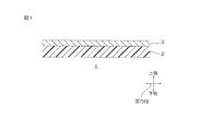
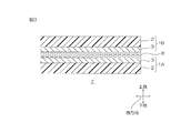
本発明の一実施形態である光透過性導電フィルム1は、例えば調光装置に用いられるフィルムである。光透過性導電フィルム1は、図1に示すように、所定の厚みを有するフィルム形状(シート形状を含む)をなし、上下方向(厚み方向)と直交する面方向に延び、平坦な上面(厚み方向一方面)および平坦な下面(厚み方向他方面)を有する。光透過性導電フィルム1は、例えば、調光フィルム7(後述、図3参照)および調光装置(後述)などの一部品であり、つまり、調光フィルム7および調光装置ではない。すなわち、光透過性導電フィルム1は、調光フィルム7および調光装置を作製するための部品であり、調光機能層8などを含まず、部品単独で流通し、産業上利用可能なデバイスである。
光透過性基材2は、光透過性導電フィルム1の最下層であって、光透過性導電フィルム1の機械的強度を確保する支持材である。
光透過性導電層3は、必要により後の工程でエッチングによりパターニングすることができる導電層である。
次に、光透過性導電フィルム1を製造する方法について説明する。
上記変化率ΔTが上記範囲であれば、光透過性導電フィルム1を長期使用しても、光透過率の変化が低減されるため、光透過率のムラを抑制することができる。
次に、光透過性導電フィルム1を用いて調光フィルム7を製造する方法について図3を参照して説明する。
図1の実施形態では、光透過性基材2の上面に光透過性導電層3が直接配置されているが、例えば、図示しないが、光透過性基材2の上面および/または下面に、機能層を設けることができる。
厚み188μmのポリエチレンテレフタレート(PET)フィルムを準備し、光透過性基材とした。
スパッタリング条件を表1に記載の条件に変更した以外は、実施例1と同様にして、光透過性導電フィルムを製造した。
スパッタリング条件を表1に記載の条件に変更した以外は、実施例1と同様にして、光透過性導電フィルムを製造した。ただし、光透過性導電層の厚みは、25nmとした。
(1)厚み
光透過性基材の厚みは、膜厚計(尾崎製作所社製、装置名「デジタルダイアルゲージ DG-205」)を用いて測定した。光透過性導電層の厚みは、透過型電子顕微鏡(日立製作所製、装置名「HF-2000」)を用いた断面観察により測定した。
各実施例および各比較例の光透過性導電フィルムにおいて、透過型電子顕微鏡(日立社製、「H-7650」)を用いて、光透過性導電層の上面を観察し、倍率:100,000倍の平面画像を得た。この画像から、光透過性導電層全体に対する結晶質領域の面積割合、および、結晶粒の最大長さを測定した。結果を表1に示す。
各光透過性導電フィルムにおいて、光透明導電層の上面の表面抵抗値を4端子法にて測定し、この表面抵抗値と上記厚みとの積により、比抵抗を算出した。結果を表1に示す。
各光透過性導電フィルムを、大気環境下で、80℃で240時間加熱した。この高温処理済みの光透過性導電フィルムにおいて、上記(2)の測定と同様にして、結晶質領域の面積割合、および、結晶粒の最大長さを測定した。その結果を表1に示す。
ヘーズメーター(スガ試験機社製、装置名「HGM-2DP)を用いて、各光透過性導電フィルムの全光線透過率を測定して、長期加熱保存前の光透過率T0とした。
調光機能層用の液晶組成物として、ネマチック液晶と樹脂と水とを混合した水性塗工液を用意し、この水性塗工液を、各実施例および各比較例の光透過性導電フィルムの光透過化性導電層の上面に、厚み20μmとなるように均一に塗布した。

2 光透過性基材
3 光透過性導電層
4 結晶質領域
5 非晶質領域
6 結晶粒
7 調光フィルム
8 調光機能層
Claims (5)
- 光透過性基材と、光透過性導電層とを備える光透過性導電フィルムであって、
前記光透過性導電層は、結晶質領域および非晶質領域を有し、
前記光透過性導電層における結晶粒の最大長が、200nm以下であり、
前記光透過性導電層を大気雰囲気で80℃、240時間の条件で加熱した際における結晶粒の最大長が、200nm以下であることを特徴とする、光透過性導電フィルム。 - 前記光透過性導電層における結晶質領域の面積割合が、25%以下であることを特徴とする、請求項1に記載の光透過性導電フィルム。
- 前記光透過性導電フィルムにおける透過率T0と、前記光透過性導電フィルムを大気雰囲気で80℃、240時間の条件で加熱した際における透過率T1との変化率が、1.0%以下であることを特徴とする、請求項1に記載の光透過性導電フィルム。
- 調光用光透過性導電フィルムである、請求項1に記載の光透過性導電フィルム。
- 第1の光透過性導電フィルムと、調光機能層と、第2の光透過性導電フィルムとを順に備え、
前記第1の光透過性導電フィルムおよび/または前記第2の光透過性導電フィルムは、請求項1に記載の光透過性導電フィルムであることを特徴とする、調光フィルム。
Priority Applications (4)
| Application Number | Priority Date | Filing Date | Title |
|---|---|---|---|
| CN201980040958.4A CN112384848A (zh) | 2018-08-06 | 2019-07-17 | 透光性导电薄膜及调光薄膜 |
| KR1020207035213A KR20210036871A (ko) | 2018-08-06 | 2019-07-17 | 광 투과성 도전 필름 및 조광 필름 |
| JP2019548353A JPWO2020031632A1 (ja) | 2018-08-06 | 2019-07-17 | 光透過性導電フィルムおよび調光フィルム |
| JP2023183876A JP2024012384A (ja) | 2018-08-06 | 2023-10-26 | 光透過性導電フィルムおよび調光フィルム |
Applications Claiming Priority (2)
| Application Number | Priority Date | Filing Date | Title |
|---|---|---|---|
| JP2018-147710 | 2018-08-06 | ||
| JP2018147710 | 2018-08-06 |
Publications (1)
| Publication Number | Publication Date |
|---|---|
| WO2020031632A1 true WO2020031632A1 (ja) | 2020-02-13 |
Family
ID=69414743
Family Applications (1)
| Application Number | Title | Priority Date | Filing Date |
|---|---|---|---|
| PCT/JP2019/028026 Ceased WO2020031632A1 (ja) | 2018-08-06 | 2019-07-17 | 光透過性導電フィルムおよび調光フィルム |
Country Status (5)
| Country | Link |
|---|---|
| JP (2) | JPWO2020031632A1 (ja) |
| KR (1) | KR20210036871A (ja) |
| CN (1) | CN112384848A (ja) |
| TW (1) | TWI834697B (ja) |
| WO (1) | WO2020031632A1 (ja) |
Cited By (4)
| Publication number | Priority date | Publication date | Assignee | Title |
|---|---|---|---|---|
| WO2024166684A1 (ja) * | 2023-02-08 | 2024-08-15 | 日東電工株式会社 | 調光フィルム |
| WO2024166683A1 (ja) * | 2023-02-08 | 2024-08-15 | 日東電工株式会社 | 調光フィルム |
| JP7549117B1 (ja) | 2023-12-21 | 2024-09-10 | 日東電工株式会社 | 調光フィルム |
| JP7561957B1 (ja) | 2023-12-21 | 2024-10-04 | 日東電工株式会社 | 調光フィルム |
Citations (3)
| Publication number | Priority date | Publication date | Assignee | Title |
|---|---|---|---|---|
| JPH08201827A (ja) * | 1995-01-31 | 1996-08-09 | Teijin Ltd | 透明導電フィルム |
| JP2004247220A (ja) * | 2003-02-14 | 2004-09-02 | Toppan Printing Co Ltd | 積層体、電極および画像表示素子 |
| JP2016157021A (ja) * | 2015-02-25 | 2016-09-01 | 日東電工株式会社 | 電界駆動型調光素子用透明導電性フィルム、調光フィルム、および電界駆動型調光素子 |
Family Cites Families (3)
| Publication number | Priority date | Publication date | Assignee | Title |
|---|---|---|---|---|
| WO2008075773A1 (ja) | 2006-12-21 | 2008-06-26 | Hitachi Chemical Co., Ltd. | 調光フィルム及び調光ガラス |
| CN101719493B (zh) * | 2008-10-08 | 2014-05-14 | 株式会社半导体能源研究所 | 显示装置 |
| JP6412539B2 (ja) * | 2015-11-09 | 2018-10-24 | 日東電工株式会社 | 光透過性導電フィルムおよび調光フィルム |
-
2019
- 2019-07-17 CN CN201980040958.4A patent/CN112384848A/zh active Pending
- 2019-07-17 WO PCT/JP2019/028026 patent/WO2020031632A1/ja not_active Ceased
- 2019-07-17 KR KR1020207035213A patent/KR20210036871A/ko not_active Ceased
- 2019-07-17 JP JP2019548353A patent/JPWO2020031632A1/ja active Pending
- 2019-07-25 TW TW108126321A patent/TWI834697B/zh active
-
2023
- 2023-10-26 JP JP2023183876A patent/JP2024012384A/ja active Pending
Patent Citations (3)
| Publication number | Priority date | Publication date | Assignee | Title |
|---|---|---|---|---|
| JPH08201827A (ja) * | 1995-01-31 | 1996-08-09 | Teijin Ltd | 透明導電フィルム |
| JP2004247220A (ja) * | 2003-02-14 | 2004-09-02 | Toppan Printing Co Ltd | 積層体、電極および画像表示素子 |
| JP2016157021A (ja) * | 2015-02-25 | 2016-09-01 | 日東電工株式会社 | 電界駆動型調光素子用透明導電性フィルム、調光フィルム、および電界駆動型調光素子 |
Cited By (8)
| Publication number | Priority date | Publication date | Assignee | Title |
|---|---|---|---|---|
| WO2024166684A1 (ja) * | 2023-02-08 | 2024-08-15 | 日東電工株式会社 | 調光フィルム |
| WO2024166683A1 (ja) * | 2023-02-08 | 2024-08-15 | 日東電工株式会社 | 調光フィルム |
| KR20240148442A (ko) * | 2023-02-08 | 2024-10-11 | 닛토덴코 가부시키가이샤 | 조광 필름 |
| KR102792308B1 (ko) | 2023-02-08 | 2025-04-08 | 닛토덴코 가부시키가이샤 | 조광 필름 |
| JP7549117B1 (ja) | 2023-12-21 | 2024-09-10 | 日東電工株式会社 | 調光フィルム |
| JP7561957B1 (ja) | 2023-12-21 | 2024-10-04 | 日東電工株式会社 | 調光フィルム |
| JP2025099489A (ja) * | 2023-12-21 | 2025-07-03 | 日東電工株式会社 | 調光フィルム |
| JP2025099490A (ja) * | 2023-12-21 | 2025-07-03 | 日東電工株式会社 | 調光フィルム |
Also Published As
| Publication number | Publication date |
|---|---|
| JPWO2020031632A1 (ja) | 2021-08-02 |
| KR20210036871A (ko) | 2021-04-05 |
| CN112384848A (zh) | 2021-02-19 |
| JP2024012384A (ja) | 2024-01-30 |
| TW202016337A (zh) | 2020-05-01 |
| TWI834697B (zh) | 2024-03-11 |
Similar Documents
| Publication | Publication Date | Title |
|---|---|---|
| JP2024012384A (ja) | 光透過性導電フィルムおよび調光フィルム | |
| JP6637565B2 (ja) | 光透過性導電フィルム | |
| EP1944386B1 (en) | Transparent conductive film and method for producing the same | |
| CN103282539B (zh) | 透明导电性薄膜及其制造方法 | |
| US20090117405A1 (en) | Transparent crystalline electrically-conductive thin film, method of production thereof, transparent electrically-conductive film, and touch panel | |
| WO2017082229A1 (ja) | 光透過性導電フィルムおよび調光フィルム | |
| JP2008520463A (ja) | 可撓性の、機械的に補償された透明積層物質を調製する方法 | |
| KR102633881B1 (ko) | 광투과성 도전 필름, 그 제조 방법, 조광 필름, 및 조광 부재 | |
| TWI770166B (zh) | 附透光性導電層之膜、調光膜及調光裝置 | |
| WO2018207622A1 (ja) | 光透過性導電層付きフィルム、調光フィルムおよび調光装置 | |
| JP6126395B2 (ja) | 透明電極付き基板の製造方法 | |
| KR102698069B1 (ko) | 투명 도전성 필름 | |
| KR102618094B1 (ko) | 광 투과성 도전 필름, 그 제조 방법, 조광 필름, 및 조광 부재 | |
| JP7418506B1 (ja) | 透明導電性フィルム | |
| KR20240124201A (ko) | 조광 필름 | |
| KR101991047B1 (ko) | 전도성 적층체, 이의 제조방법, 이를 포함하는 투명 전극 및 전자소자 |
Legal Events
| Date | Code | Title | Description |
|---|---|---|---|
| ENP | Entry into the national phase |
Ref document number: 2019548353 Country of ref document: JP Kind code of ref document: A |
|
| 121 | Ep: the epo has been informed by wipo that ep was designated in this application |
Ref document number: 19846477 Country of ref document: EP Kind code of ref document: A1 |
|
| ENP | Entry into the national phase |
Ref document number: 20207035213 Country of ref document: KR Kind code of ref document: A |
|
| NENP | Non-entry into the national phase |
Ref country code: DE |
|
| 122 | Ep: pct application non-entry in european phase |
Ref document number: 19846477 Country of ref document: EP Kind code of ref document: A1 |