WO2020031521A1 - 配線基板およびその製造方法 - Google Patents
配線基板およびその製造方法 Download PDFInfo
- Publication number
- WO2020031521A1 WO2020031521A1 PCT/JP2019/024627 JP2019024627W WO2020031521A1 WO 2020031521 A1 WO2020031521 A1 WO 2020031521A1 JP 2019024627 W JP2019024627 W JP 2019024627W WO 2020031521 A1 WO2020031521 A1 WO 2020031521A1
- Authority
- WO
- WIPO (PCT)
- Prior art keywords
- insulator
- conductor
- insulators
- wiring board
- hole
- Prior art date
- Legal status (The legal status is an assumption and is not a legal conclusion. Google has not performed a legal analysis and makes no representation as to the accuracy of the status listed.)
- Ceased
Links
Images





Classifications
-
- H—ELECTRICITY
- H05—ELECTRIC TECHNIQUES NOT OTHERWISE PROVIDED FOR
- H05K—PRINTED CIRCUITS; CASINGS OR CONSTRUCTIONAL DETAILS OF ELECTRIC APPARATUS; MANUFACTURE OF ASSEMBLAGES OF ELECTRICAL COMPONENTS
- H05K3/00—Apparatus or processes for manufacturing printed circuits
- H05K3/40—Forming printed elements for providing electric connections to or between printed circuits
- H05K3/42—Plated through-holes or plated via connections
-
- H—ELECTRICITY
- H10—SEMICONDUCTOR DEVICES; ELECTRIC SOLID-STATE DEVICES NOT OTHERWISE PROVIDED FOR
- H10W—GENERIC PACKAGES, INTERCONNECTIONS, CONNECTORS OR OTHER CONSTRUCTIONAL DETAILS OF DEVICES COVERED BY CLASS H10
- H10W70/00—Package substrates; Interposers; Redistribution layers [RDL]
- H10W70/60—Insulating or insulated package substrates; Interposers; Redistribution layers
- H10W70/67—Insulating or insulated package substrates; Interposers; Redistribution layers characterised by their insulating layers or insulating parts
- H10W70/69—Insulating materials thereof
- H10W70/692—Ceramics or glasses
Definitions
- the present technology relates to a wiring board. More specifically, the present invention relates to a wiring board having a hole penetrating a base material and a method of manufacturing the wiring board.
- silicon and glass are attracting attention as materials for semiconductor substrates that can replace organic materials. Since these materials have greatly reduced expansion and contraction due to moisture absorption and temperature as compared with organic materials, they have great merits in terms of formation of fine wiring and connection reliability with a semiconductor chip.
- a substrate made of silicon can form finer wiring than a glass substrate using the know-how of semiconductor chip production, and furthermore, a through-silicon-via (TSV) can be formed.
- TSV through-silicon-via
- the silicon substrate is a semiconductor
- the glass substrate is an insulator, so that even in a high-speed transmission circuit, there is no concern about the occurrence of parasitic capacitance, and the electrical characteristics are more excellent.
- the step of forming an insulating film on the surface thereof is unnecessary, so that the insulating reliability is essentially high and the steps are advantageously shortened.
- the embedding resin is recessed, so that the via wiring portion and the front and back surface wiring portion are not immersed.
- a wiring board having a large contact area has been proposed (for example, see Patent Document 1).
- the present technology has been developed in view of such a situation, and has an object to secure the functionality of an embedding resin with a simple structure in a wiring board and improve reliability.
- the present technology has been made in order to solve the above-described problem, and a first aspect thereof includes a base material, a hole penetrating the base material, and a conductor formed along a side wall of the hole. And a plurality of types of insulators filled inside the conductor. Thereby, there is an effect that a plurality of types of insulators are filled inside the through-hole and the properties of the respective insulators are exhibited.
- a specific type of insulator among the plurality of types of insulators has higher adhesion than other types of insulators, and the other type of insulator is the specific type of insulator.
- An insulator having a lower expansion coefficient than that of the type of insulator may be used. This brings about the effect of exhibiting the properties of both insulators such as high adhesion and low expansion coefficient.
- the specific type of insulator may cover the conductor, and the other type of insulator may be formed inside the conductor.
- the specific type of insulator may include a portion connected to each other in the hole radial direction inside the conductor.
- the area ratio of the specific type of insulator to the other type of insulator in the hole diameter direction may change with respect to the penetration direction.
- the other type of insulator may include a granular type of insulator different from the specific type of insulator.
- the specific type of insulator may be a granular insulator, and the other type of insulator may be filled in a gap between the granular insulators.
- the granular insulator may have a state of being deformed along the shape of the conductor at a contact portion with the conductor, and may have a shape that is different from that of the other granular insulator. May have a state deformed along each other's shape at the contact portion. This provides an effect of reducing the influence of expansion while ensuring adhesion.
- the first side surface may further include another conductor that closes one opening of the through hole. That is, the present invention may be applied to a bottomed via structure.
- the base material may be silicon or glass. These are materials having a low coefficient of linear expansion, but by filling a plurality of types of insulators inside the through holes, an effect of adjusting the affinity between the base material and the insulators is brought about.
- a second aspect of the present technology includes a step of attaching a sheet material made of a plurality of types of insulators to at least one surface of a base material including a through hole and a conductor formed along a side wall of the hole. Applying a pressure under vacuum to fill the inside of the conductor with the sheet material. This brings about an effect that a plurality of types of insulators are filled by a simple method.
- a plurality of types of insulators including a granular insulator from one side of a base material including a through hole and a conductor formed along a side wall of the hole. And a step of applying pressure from one surface of the base material to the plurality of types of insulators inside the conductor. This brings about an effect that a plurality of types of insulators are filled by a simple method.
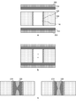
- FIG. 2 is a cross-sectional view illustrating a configuration example of a wiring board 10 according to the first embodiment of the present technology.
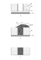
- FIG. 5 is a process diagram illustrating an example of a method for manufacturing the wiring board 10 according to the first embodiment of the present technology.
- FIG. 5 is a cross-sectional view illustrating another example of the structure of the wiring board 10 according to the first embodiment of the present technology.
- FIG. 9 is a cross-sectional view illustrating still another example of the structure of the wiring board 10 according to the first embodiment of the present technology. It is a figure showing an example of structure of wiring board 10 in a 2nd embodiment of this art.
- FIG. 11 is a process diagram illustrating an example of a method for manufacturing a wiring board 10 according to the second embodiment of the present technology.
- FIG. 11 is a process diagram illustrating an example of a method for manufacturing a wiring board 10 according to the second embodiment of the present technology.
- FIG. 14 is a cross-sectional view illustrating another example of the structure of the wiring board 10 according to the second embodiment of the present technology.
- FIG. 11 is a cross-sectional view illustrating still another example of the structure of the wiring board 10 according to the second embodiment of the present technology.
- FIG. 9 is a process diagram illustrating a first modification of the method of manufacturing wiring substrate 10 in the embodiment of the present technology.
- FIG. 9 is a process diagram illustrating a second modification of the method of manufacturing the wiring board 10 according to the embodiment of the present technology.
- FIG. 1 is a cross-sectional view illustrating a structural example of a wiring board 10 according to the first embodiment of the present technology.
- the wiring substrate 10 is assumed to be a material having a low coefficient of thermal expansion (CTE) such as glass or silicon as the base material 100.
- the wiring board 10 includes a through-hole (via) 110 penetrating from the front surface of the base material 100 to the back surface.
- a conductor 120 is formed inside the through hole 110 along the side wall.
- a conductive metal such as copper (Cu) is used.
- the conductor 120 is formed as a copper film, for example, by forming a copper sputtered film by sputtering over the entire surface and immersing the film in a plating solution for growth.
- the wiring board 10 of the first embodiment has a multiplex structure in which the resin is embedded in the through hole 110 in a coaxial shape.
- insulators 210 and 220 are shown.
- the specific type of insulator 210 one having higher adhesion than other types of insulators 220 is employed.
- insulator 220 one having a lower expansion coefficient than the specific type of insulator 210 is employed.
- a photosensitive sheet resist having a two-layer structure of the insulators 210 and 220 is encapsulated in the through holes 110 by a vacuum lamination method.
- Aa in the figure shows an example in which the inner insulator 220 is divided by the outer insulator 210. That is, the specific type of insulator 210 includes portions that are connected to each other in the radial direction of the through hole 110 inside the conductor 120.
- ⁇ Circle around (b) ⁇ shows an example in which the inner insulator 220 is not divided by the outer insulator 210. That is, another type of insulator 220 includes a portion that is connected to the inside of the conductor 120 in the through direction (depth direction) of the through hole 110.
- the insulators 210 and 220 can assume any of the states a and b in FIG. In any case, the insulator 210 covers the conductor 120, and the insulator 220 is formed inside the conductor 120.
- the ratio of the cross-sectional area of the outer insulator 210 to the inner insulator 220 in the hole diameter direction changes in the penetration direction (depth direction). That is, as shown by a and b in the figure, the areas of the insulators 210 and 220 are not uniform.
- the wiring board 10 may be used as a part of a laminated board by being laminated with another wiring board.
- FIG. 2 is a process diagram illustrating an example of a method for manufacturing the wiring board 10 according to the first embodiment of the present technology.
- a photosensitive sheet resist having a two-layer structure of insulators 210 and 220 is bonded to the front and back surfaces of the base material 100 as shown in FIG. At this time, the front and back of the photosensitive sheet resist are determined such that the insulator 210 having high adhesion comes into contact with the base material 100.
- a silicon-based stress relaxation material is given.
- Specific product names include "one-pack elastomer type JCR6101 @ UP" (Toray).
- the CTE is 300 ppm and the Young's modulus is about 1.2 MPa.
- the insulator 220 is laminated with the insulator 210, processed into a film shape, and simultaneously filled by a vacuum lamination method.
- a conventional resin having high adhesion and a low dielectric constant can be used. Further, as described later, after the insulator 210 is first filled, opening processing is performed with a laser or the like, and then the insulator 220 may be injected in a liquid state using a dispenser or the like.
- FIG. 3 is a cross-sectional view illustrating another example of the structure of the wiring board 10 according to the first embodiment of the present technology.
- the example in which the insulators 210 and 220 are filled from both surfaces of the base material 100 has been described.
- the insulators 210 and 220 may be filled from only one surface of the base material 100.
- a structure (a bottomed via structure) in which the conductor 120 is formed so as to close one opening of the through hole 110 is assumed.
- a photosensitive sheet resist is attached to one surface of the base material 100, and pressure is applied under vacuum.
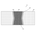
- FIG. 4 is a cross-sectional view illustrating still another example of the structure of the wiring board 10 according to the first embodiment of the present technology.
- the shape of the through hole 110 is assumed to be a hole vertically penetrating the base material 100.
- a part of the through hole 110 has a constricted shape.
- the conductor 120 since the conductor 120 is formed along the side wall of the through hole 110, the conductor 120 similarly has a constricted shape.
- the photosensitive sheet resist having the two-layer structure of the insulators 210 and 220 is attached to the base material 100, and the through holes 110 are filled by the vacuum lamination method.
- insulators 210 and 220 having different properties can be filled in through-hole 110 by a simple method.
- FIG. 5 is a diagram illustrating a configuration example of the wiring board 10 according to the second embodiment of the present technology.
- a is a sectional view
- b is a top view.
- the wiring substrate 10 according to the second embodiment uses a material having a low coefficient of linear expansion such as glass or silicon as the base material 100, and a through hole 110 penetrating from the front surface to the back surface of the base material 100 and the side wall thereof.
- the second embodiment is the same as the first embodiment in that a conductor 120 is provided.
- insulators 230 and 240 are shown.
- the specific type of insulator 230 one having higher adhesion than the other type of insulator 240 is employed.
- insulator 240 one having a lower expansion coefficient than the specific type of insulator 230 is employed. That is, the relationship between them is the same as that of the insulators 210 and 220 in the above-described first embodiment.
- the insulator 230 is granular insulating particles.
- the insulator 240 is a resin that fills a gap between the insulators 230.
- the insulator 240 may be a gap such as a vacuum layer.
- the insulators 230 and 240 are filled in the through holes 110 by the squeegee method. Assuming that an organic material is used as the insulator 230, by applying heat after filling, a part of the insulator 230 is melted, and as shown in FIG. Has a state deformed along the shape of the conductor 120. Similarly, the insulator 230 has a state of being deformed along the shape of each other at a contact portion with another granular insulator 230.
- FIG. 6 is a process diagram illustrating an example of a method for manufacturing the wiring substrate 10 according to the second embodiment of the present technology.
- the cover sheet 310 is bonded to the back surface of the base material 100.
- insulators 230 and 240 are supplied inside conductor 120, pressure is applied by squeegee 410, and overflow of insulators 230 and 240 is removed (squeegee method). ).
- the base material 100 is heated in the baking process, and then the cover sheet 310 is removed.
- Specific examples of the insulator 230 include resin beads.
- Specific product names include Technopolymer ARX and AEX (Sekisui Chemical).
- silica beads can be mentioned as a resin having a linear expansion coefficient close to that of glass.
- Specific product names include silica spherical fine particles (Nippon Steel & Sumikin Materials Corporation).
- the average particle size is as small as 0.2 ⁇ m, and is sufficiently small for TGV filling.
- the particles become amorphous, and the CTE is as small as about 0.5 ppm.
- the alignment can be performed by, for example, setting the filling rate to about 50% and filling the empty wall with a resin.
- the adjustment of the filling rate may be performed by mixing a large-diameter product and a small-diameter product of silica particles.
- the gap may be left as a space using silica particles coated with a thin film of resin.
- FIG. 7 is a cross-sectional view illustrating another example of the structure of the wiring board 10 according to the second embodiment of the present technology.
- a bottomed via structure can be assumed, as in the first embodiment.
- the insulators 230 and 240 are supplied from the openings that are not closed by the conductors 120 in the through holes 110, and pressure is applied.
- FIG. 8 is a cross-sectional view illustrating still another example of the structure of the wiring board 10 according to the second embodiment of the present technology.
- a constricted structure can be assumed as the shape of the through-hole 110, as in the first embodiment. With this constricted structure, an effect of suppressing the influence of the expansion force due to the insulators 230 and 240 filling the through hole 110 is obtained.
- the insulators 230 and 240 are filled in the through holes 110 by the squeegee method. Accordingly, insulators 230 and 240 having different properties can be filled in through-hole 110 by a simple method.
- the inside of the conductor 120 of the through hole 110 is filled with an insulator using a photosensitive sheet resist or insulating particles.
- an insulator is filled, an opening is formed by a laser or the like, and another insulator is injected.
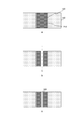
- FIG. 9 is a process diagram illustrating a first modification of the method of manufacturing wiring substrate 10 according to the embodiment of the present technology.
- the insulator 210 is filled inside the conductor 120 of the through hole 110 as shown in FIG. Then, as shown by b in the figure, an opening process is performed by a laser or the like. Thereafter, the insulator 220 is injected into the opening as shown in FIG. Thereby, the two types of insulators 210 and 220 can be filled inside the conductor 120 of the through hole 110.
- FIG. 10 is a process diagram illustrating a second modification of the method of manufacturing wiring substrate 10 according to the embodiment of the present technology.
- an insulator 210 is filled inside the conductor 120 of the through hole 110 as shown in FIG. Opening is performed by, for example, Thereafter, as shown in FIG. 3C, the openings are filled with insulators 230 and 240.
- the insulators 230 and 240 are the two types of insulators 230 and 240 in the above-described second embodiment. Therefore, this allows the three types of insulators 210, 230 and 240 to fill the inside of the conductor 120 of the through hole 110.
- the present technology may have the following configurations.
- the specific type of insulator covers the conductor; The wiring board according to (2), wherein the other type of insulator is formed inside the conductor.
Landscapes
- Engineering & Computer Science (AREA)
- Manufacturing & Machinery (AREA)
- Microelectronics & Electronic Packaging (AREA)
- Printing Elements For Providing Electric Connections Between Printed Circuits (AREA)
- Structure Of Printed Boards (AREA)
Abstract
配線基板において簡易な構造により包理樹脂の機能性を確保して、信頼性を向上させる。 配線基板は、基材を貫通する貫通孔と、その貫通孔の側壁に沿って形成された導体とを備える。この配線基板においては、貫通孔の側壁に沿って形成された導体の内側に、複数種類の絶縁体が充填される。複数種類の絶縁体のうち特定の種類の絶縁体は、他の種類の絶縁体よりも密着性を高くすることができる。他の種類の絶縁体は、特定の種類の絶縁体よりも膨張率を低くすることができる。このように複数種類の絶縁体を充填することにより、包理樹脂の機能性を確保する。
Description
本技術は、配線基板に関する。詳しくは、基材を貫通する孔を備える配線基板およびその製造方法に関する。
近年、半導体チップおよび外部接続装置を用いた半導体装置は、電子機器、自動車等の多くの製品に用いられている。そして、それらの製品の高性能化、小型化、軽量化が進むなかで、半導体装置の小型化、多ピン化、外部接続端子のファインピッチ化が求められている。従来、半導体基板の材料としては、エポキシ樹脂およびそれをガラス繊維に含浸させたガラエポ材料など、有機材料が多く用いられてきた。この有機材料においては、その多くについて、吸水率が比較的高く、また、シリコン製の半導体チップと比較して温度による収縮や膨張が大きいため、半導体チップとスケールの整合をとった微細配線の形成が困難であった。また、半導体チップと接続した後の信頼性の確保という面で問題を有していた。
そこで、有機材料に代わる半導体基板の材料として、シリコンやガラスが注目されている。これらは、吸湿、温度による伸縮が、有機材料と比べて、大きく低減されているため、微細配線の形成、および、半導体チップとの接続信頼性という面で、大きなメリットを有している。
両者を比較すると、シリコンを材料とする基板は、半導体チップ製造のノウハウを利用して、ガラス基板よりもさらに微細な配線形成が可能であり、さらに貫通電極(TSV:Through-Silicon-Via)形成プロセスも確立されているという長所がある。一方、シリコンの形状が円盤型に限定され、ウェハー周辺部が利用できず、また、大型サイズでの製造が困難であるという短所もある。これに対して、ガラス基板においては、未だ製造プロセスが確立していない反面、ディスプレイ材料などでのノウハウを利用しての大型化が可能である。さらに、電気特性での比較を考えると、シリコン基板が半導体なのに対し、ガラス基板は絶縁体であるため、高速伝送回路においても、寄生容量発生の懸念がなく、より電気特性に優れているといえる。そもそも、ガラス基板の場合は、その表面に絶縁膜を形成する工程自体が不要であるため、本質的に絶縁信頼性が高く、また、工程の短縮という点においても有利である。
以上のように、多くの利点を持つガラス基板であるが、製造プロセスがまだ十分に確立していないという問題がある。とくに、その脆性ゆえに、表面の電気的導通をとるのに必要な貫通電極(TGV:Through-Glass-Via)の形成に困難性が伴う点と、配線材料の主流である銅との密着が弱いことによる、配線形成の確実性が高くない点とに課題がある。
このようなガラス基板について、ガラス基板表裏面と貫通孔内の導電層との間の接続信頼性を向上させるために、包理樹脂をへこませて、ビア配線部と表裏面配線部との接触面積を広くした配線基板が提案されている(例えば、特許文献1参照。)。
上述の従来技術では、ビア配線部と表裏面配線部との接触面積を広くすることにより配線間の剥離を抑制している。しかしながら、この上述の従来技術では、へこみを設けるための工程が増えるとともに、へこみ量の管理も難しくなり、歩留りが低下するなどの問題がある。
本技術はこのような状況に鑑みて生み出されたものであり、配線基板において簡易な構造により包理樹脂の機能性を確保して、信頼性を向上させることを目的とする。
本技術は、上述の問題点を解消するためになされたものであり、その第1の側面は、基材と、上記基材を貫通する孔と、上記孔の側壁に沿って形成された導体と、上記導体の内側に充填された複数種類の絶縁体とを具備する配線基板である。これにより、複数種類の絶縁体を貫通孔の内側に充填して、それぞれの絶縁体による性質を発揮させるという作用をもたらす。
また、この第1の側面において、上記複数種類の絶縁体のうち特定の種類の絶縁体は、他の種類の絶縁体よりも密着性が高く、上記他の種類の絶縁体は、上記特定の種類の絶縁体よりも膨張率が低いものを利用してもよい。これにより、高い密着性と低膨張率という両者の絶縁体による性質を発揮させるという作用をもたらす。
また、この第1の側面において、上記特定の種類の絶縁体は、上記導体を被覆し、上記他の種類の絶縁体は、上記導体の内側に形成されてもよい。これにより、導体との密着性を確保しながら、膨張による影響を低減するという作用をもたらす。
また、この第1の側面において、上記特定の種類の絶縁体は、上記導体の内側において互いに孔径方向に繋がる部分を備えてもよい。
また、この第1の側面において、上記特定の種類の絶縁体と上記他の種類の絶縁体の孔径方向における面積比は、貫通方向に対して変化するようにしてもよい。
また、この第1の側面において、上記他の種類の絶縁体は、上記特定の種類の絶縁体とは異なる種類の粒状の絶縁体を含んでもよい。
また、この第1の側面において、上記特定の種類の絶縁体は、粒状の絶縁体であり、上記他の種類の絶縁体は、上記粒状の絶縁体の隙間に充填されてもよい。これにより、粒状の絶縁体により導体との密着性を確保しながら、膨張による影響を低減するという作用をもたらす。
また、この第1の側面において、上記粒状の絶縁体は、上記導体との接触部において上記導体の形状に沿って変形した状態を有してもよく、また、他の上記粒状の絶縁体との接触部において互いの形状に沿って変形した状態を有してもよい。これにより、密着性を確保しながら、膨張による影響を低減するという作用をもたらす。
また、この第1の側面において、上記貫通する孔の一方の開口部を塞ぐ他の導体をさらに具備してもよい。すなわち、有底ビア構造に適用してもよい。
また、この第1の側面において、上記基材は、シリコンまたはガラスであってもよい。これらは線膨張率の低い材料であるが、貫通孔の内側に複数種類の絶縁体を充填することにより、基材と絶縁体との親和性を調整するという作用をもたらす。
また、本技術の第2の側面は、貫通する孔と上記孔の側壁に沿って形成された導体とを備える基材の少なくとも一方の面に複数種類の絶縁体からなるシート材を貼る工程と、真空下で圧力を加えて上記シート材を上記導体の内側に充填させる工程とを具備する配線基板の製造方法である。これにより、簡易な手法により複数種類の絶縁体を充填させるという作用をもたらす。
また、本技術の第3の側面は、貫通する孔と上記孔の側壁に沿って形成された導体とを備える基材の一方の面から粒状の絶縁体を含む複数種類の絶縁体を上記導体の内側に供給する工程と、上記基材の一方の面から上記導体の内側の上記複数種類の絶縁体に圧力を印加する工程とを具備する配線基板の製造方法である。これにより、簡易な手法により複数種類の絶縁体を充填させるという作用をもたらす。
本技術によれば、配線基板において簡易な構造により包理樹脂の機能性を確保して、信頼性を向上させることができるという優れた効果を奏し得る。なお、ここに記載された効果は必ずしも限定されるものではなく、本開示中に記載されたいずれかの効果であってもよい。
以下、本技術を実施するための形態(以下、実施の形態と称する)について説明する。説明は以下の順序により行う。
1.第1の実施の形態(充填材料として感光性シートレジストを用いた例)
2.第2の実施の形態(充填材料として絶縁粒子を用いた例)
3.変形例(レーザによる開口加工を用いた例)
1.第1の実施の形態(充填材料として感光性シートレジストを用いた例)
2.第2の実施の形態(充填材料として絶縁粒子を用いた例)
3.変形例(レーザによる開口加工を用いた例)
<1.第1の実施の形態>
[配線基板の構造]
図1は、本技術の第1の実施の形態における配線基板10の構造例を示す断面図である。
[配線基板の構造]
図1は、本技術の第1の実施の形態における配線基板10の構造例を示す断面図である。
この配線基板10は、基材100として、ガラスやシリコンなどの線膨張率(CTE:Coefficient of Thermal Expansion)の低い材料を想定する。この配線基板10は、基材100の表面から裏面に貫通する貫通孔(ビア)110を備える。
貫通孔110の内側には、側壁に沿って導体120が形成される。この導体120としては、例えば銅(Cu)などの伝導金属が用いられる。この導体120は、例えば、全面スパッタにより銅のスパッタ膜を形成し、めっき溶液に浸して成長させることにより、銅被膜として形成される。
基材100として、線膨張率の低い材料を用いた場合、貫通孔110に標準的な樹脂を包埋すると、その線膨張率の差から配線が応力的なダメージを受け、導通不良が発生するおそれがある。そこで、貫通孔110の導体120の内側には、複数種類の絶縁体を充填する。すなわち、この第1の実施の形態の配線基板10は、貫通孔110に同軸形状にて樹脂を包埋させた多重構造を備える。
この例では、2種類の絶縁体210および220が示されている。特定の種類の絶縁体210は、他の種類の絶縁体220よりも密着性が高いものが採用される。他の種類の絶縁体220は、特定の種類の絶縁体210よりも膨張率が低いものが採用される。これにより、絶縁体210によって配線密着性、誘電率など、機能性を高めつつも、絶縁体220によって応力緩和などの効果を持たせることができる。そして、高い信頼性を保ちつつも、ビア設計の自由度、伝送特性などを高めることが可能となる。
この第1の実施の形態においては、絶縁体210および220の2層構造を有する感光性シートレジストを、真空ラミネート法によって貫通孔110に包理させることを想定する。
同図におけるaは、内側の絶縁体220が外側の絶縁体210によって分断されている例を示している。すなわち、特定の種類の絶縁体210は、導体120の内側において互いに貫通孔110の孔径方向に繋がる部分を備える。
一方、同図におけるbは、内側の絶縁体220が外側の絶縁体210によって分断されない例を示している。すなわち、他の種類の絶縁体220は、導体120の内側において互いに貫通孔110の貫通方向(深さ方向)に繋がる部分を備える。
この第1の実施の形態では、絶縁体210および220は、同図におけるaおよびbのいずれの状態も想定し得る。いずれにおいても、絶縁体210は導体120を被覆し、絶縁体220は導体120の内側に形成される。
外側の絶縁体210と内側の絶縁体220の孔径方向における断面積の比は、貫通方向(深さ方向)に対して変化する。すなわち、同図におけるaおよびbに示すように、絶縁体210および220の面積は一様ではない。
なお、この例では1つの配線基板10について示しているが、他の配線基板と積層して積層基板の一部として配線基板10を用いてもよい。
[配線基板の製造方法]
図2は、本技術の第1の実施の形態における配線基板10の製造方法の一例を示す工程図である。
図2は、本技術の第1の実施の形態における配線基板10の製造方法の一例を示す工程図である。
同図におけるaに示すように、絶縁体210および220の2層構造を有する感光性シートレジストが、基材100の表面および裏面に貼り合わされる。その際、密着性の高い絶縁体210が基材100と接触するように、感光性シートレジストの表裏が決定される。
同図におけるbに示すように、感光性シートレジストを貼り合せた状態で、真空下で温度を上げて、圧力を印加する(真空ラミネート法)。これにより、感光性シートレジストを形成する絶縁体210および220が、貫通孔110に包理される。
その後、リソグラフィおよび現像処理により不要部分が除去されて、同図におけるcに示す多重構造が得られる。
貫通孔110の中央部に充填される絶縁体220の一例として、シリコン系の応力緩和材が挙げられる。具体的な製品名としては、「1液エラストマータイプJCR6101 UP」(東レ社)などである。この仕様の場合、CTE:300ppm、ヤング率:約1.2MPaである。この絶縁体220を絶縁体210と積層して、フィルム状に加工し、真空ラミネート法にて同時に充填させることが想定される。絶縁体210としては、従来の密着性の高い低誘電率の樹脂を用いることができる。また、後述するように、最初に絶縁体210を充填した後に、レーザーなどで開口加工を施し、その後、ディスペンサなどを用いて絶縁体220を液状で注入してもよい。
[有底ビア構造]
図3は、本技術の第1の実施の形態における配線基板10の他の構造例を示す断面図である。
図3は、本技術の第1の実施の形態における配線基板10の他の構造例を示す断面図である。
上述の例では、絶縁体210および220を基材100の両面から充填する例について説明したが、基材100の一方の面のみから充填するようにしてもよい。そのような例として、導体120が貫通孔110の一方の開口部を塞ぐように形成されている構造(有底ビア構造)を想定する。
この場合、上述の真空ラミネート法では、基材100の片面に感光性シートレジストを貼り合せて、真空下で圧力を印加することになる。
なお、この例では、貫通孔110の一方の開口部に底(導体120)を形成する例について説明したが、基材100の片面から孔を形成して、その孔の底部に導体120を形成してもよい。
[くびれ構造]
図4は、本技術の第1の実施の形態における配線基板10のさらに他の構造例を示す断面図である。
図4は、本技術の第1の実施の形態における配線基板10のさらに他の構造例を示す断面図である。
上述の例では、貫通孔110の形状として、基材100を垂直に貫通する孔を想定していた。それに対し、この構造例では、貫通孔110の一部においてくびれた形状を備える。この場合、導体120は貫通孔110の側壁に沿って形成されるため、同様にくびれた形状を備える。
このくびれ構造により、貫通孔110に充填される絶縁体210および220による膨張力の影響を抑制するという効果が得られる。
このように、本技術の第1の実施の形態では、絶縁体210および220の2層構造を有する感光性シートレジストを基材100に貼り合せて、真空ラミネート法により貫通孔110に充填する。これにより、異なる性質を有する絶縁体210および220を簡易な手法により貫通孔110に充填することができる。
<2.第2の実施の形態>
[配線基板の構造]
図5は、本技術の第2の実施の形態における配線基板10の構造例を示す図である。同図におけるaは断面図であり、bは上面図である。
[配線基板の構造]
図5は、本技術の第2の実施の形態における配線基板10の構造例を示す図である。同図におけるaは断面図であり、bは上面図である。
この第2の実施の形態における配線基板10は、基材100として、ガラスやシリコンなどの線膨張率の低い材料を使用し、基材100の表面から裏面に貫通する貫通孔110およびその側壁に導体120を備える点において、上述の第1の実施の形態と同様である。
この第2の実施の形態では、2種類の絶縁体230および240が示されている。特定の種類の絶縁体230は、他の種類の絶縁体240よりも密着性が高いものが採用される。他の種類の絶縁体240は、特定の種類の絶縁体230よりも膨張率が低いものが採用される。すなわち、両者の関係は、上述の第1の実施の形態における絶縁体210および220と同様である。
絶縁体230は、粒状の絶縁粒子である。絶縁体240は、絶縁体230の隙間を埋める樹脂である。ただし、絶縁体240は、真空層などの空隙であってもよい。
この第2の実施の形態においては、絶縁体230および240を、スキージ法により貫通孔110に充填することを想定する。絶縁体230として有機材料を想定すると、充填後に熱を加えることにより、絶縁体230の一部が溶融し、同図におけるbに示すように、貫通孔110の側壁の導体120との接触部231において導体120の形状に沿って変形した状態を有する。また、同様に、絶縁体230は他の粒状の絶縁体230との接触部において互いの形状に沿って変形した状態を有する。
[配線基板の製造方法]
図6は、本技術の第2の実施の形態における配線基板10の製造方法の一例を示す工程図である。
図6は、本技術の第2の実施の形態における配線基板10の製造方法の一例を示す工程図である。
同図におけるaに示すように、カバーシート310が、基材100の裏面に貼り合わされる。
同図におけるbに示すように、絶縁体230および240が導体120の内側に供給され、スキージ410によって圧力が印加されるとともに、絶縁体230および240のうち溢れたものは除去される(スキージ法)。
同図におけるcに示すように、ベイク処理において基材100が加熱され、その後、カバーシート310が除去される。
絶縁体230の具体例としては、樹脂ビーズが挙げられる。具体的な製品名としては、テクノポリマーARX、AEX(積水化成社)などがある。
また、ガラスと線膨張率の近い樹脂としては、例えば、シリカビーズが挙げられる。具体的な製品名としては、シリカ球状微粒子(新日鉄住金マテリアルズ社)などがある。この製品の場合、平均粒径:0.2umと小径なものもあり、TGV充填用としては、十分小さいサイズである。また、粒子は非晶質となり、CTEは約0.5ppmと非常に小さい。この場合、CTEがガラスの約3ppmより小さいため、例えば、充填率を50%程度とし、空壁を樹脂で埋めることなどにより、合わせ込みが可能である。充填率の合わせ込みは、シリカ粒子の大径品および小径品を混合して、行ってもよい。樹脂の薄膜でコーティングされたシリカ粒子を用いて、隙間は空間のままの状態でもよい。
[有底ビア構造]
図7は、本技術の第2の実施の形態における配線基板10の他の構造例を示す断面図である。
図7は、本技術の第2の実施の形態における配線基板10の他の構造例を示す断面図である。
この第2の実施の形態においても、上述の第1の実施の形態と同様に、有底ビア構造を想定することができる。この場合、上述のスキージ法では、貫通孔110における導体120によって塞がれていない開口部から、絶縁体230および240を供給し、圧力を印加することになる。
[くびれ構造]
図8は、本技術の第2の実施の形態における配線基板10のさらに他の構造例を示す断面図である。
図8は、本技術の第2の実施の形態における配線基板10のさらに他の構造例を示す断面図である。
この第2の実施の形態においても、上述の第1の実施の形態と同様に、貫通孔110の形状としてくびれ構造を想定することができる。このくびれ構造により、貫通孔110に充填される絶縁体230および240による膨張力の影響を抑制するという効果が得られる。
このように、本技術の第2の実施の形態では、絶縁体230および240をスキージ法により貫通孔110に充填する。これにより、異なる性質を有する絶縁体230および240を簡易な手法により貫通孔110に充填することができる。
<3.変形例>
上述の実施の形態では、感光性シートレジストまたは絶縁粒子を用いて、貫通孔110の導体120の内側に絶縁体を充填していた。ここでは、その変形例として、絶縁体を充填した後に、レーザーなどにより開口加工を施して、他の絶縁体を注入する例について説明する。
上述の実施の形態では、感光性シートレジストまたは絶縁粒子を用いて、貫通孔110の導体120の内側に絶縁体を充填していた。ここでは、その変形例として、絶縁体を充填した後に、レーザーなどにより開口加工を施して、他の絶縁体を注入する例について説明する。
[第1の変形例]
図9は、本技術の実施の形態における配線基板10の製造方法の第1の変形例を示す工程図である。
図9は、本技術の実施の形態における配線基板10の製造方法の第1の変形例を示す工程図である。
この例では、同図におけるaに示すように、貫通孔110の導体120の内側に絶縁体210を充填する。そして、同図におけるbに示すように、レーザーなどにより開口加工を施す。その後、同図におけるcに示すように、開口部に絶縁体220を注入する。これにより、2種類の絶縁体210および220を貫通孔110の導体120の内側に充填することができる。
[第2の変形例]
図10は、本技術の実施の形態における配線基板10の製造方法の第2の変形例を示す工程図である。
図10は、本技術の実施の形態における配線基板10の製造方法の第2の変形例を示す工程図である。
この例では、上述の第1の変形例と同様に、同図におけるaに示すように、貫通孔110の導体120の内側に絶縁体210を充填し、同図におけるbに示すように、レーザーなどにより開口加工を施す。その後、同図におけるcに示すように、開口部に絶縁体230および240を充填する。絶縁体230および240は、上述の第2の実施の形態における2種類の絶縁体230および240である。したがって、これにより、3種類の絶縁体210、230および240を貫通孔110の導体120の内側に充填することができる。
なお、上述の実施の形態は本技術を具現化するための一例を示したものであり、実施の形態における事項と、特許請求の範囲における発明特定事項とはそれぞれ対応関係を有する。同様に、特許請求の範囲における発明特定事項と、これと同一名称を付した本技術の実施の形態における事項とはそれぞれ対応関係を有する。ただし、本技術は実施の形態に限定されるものではなく、その要旨を逸脱しない範囲において実施の形態に種々の変形を施すことにより具現化することができる。
なお、本明細書に記載された効果はあくまで例示であって、限定されるものではなく、また、他の効果があってもよい。
なお、本技術は以下のような構成もとることができる。
(1)基材と、
前記基材を貫通する孔と、
前記孔の側壁に沿って形成された導体と、
前記導体の内側に充填された複数種類の絶縁体と
を具備する配線基板。
(2)前記複数種類の絶縁体のうち特定の種類の絶縁体は、他の種類の絶縁体よりも密着性が高く、
前記他の種類の絶縁体は、前記特定の種類の絶縁体よりも膨張率が低い
前記(1)に記載の配線基板。
(3)前記特定の種類の絶縁体は、前記導体を被覆し、
前記他の種類の絶縁体は、前記導体の内側に形成される
前記(2)に記載の配線基板。
(4)前記特定の種類の絶縁体は、前記導体の内側において互いに孔径方向に繋がる部分を備える
前記(3)に記載の配線基板。
(5)前記特定の種類の絶縁体と前記他の種類の絶縁体の孔径方向における面積比は、貫通方向に対して変化する
前記(3)または(4)に記載の配線基板。
(6)前記他の種類の絶縁体は、前記特定の種類の絶縁体とは異なる種類の粒状の絶縁体を含む
前記(3)に記載の配線基板。
(7)前記特定の種類の絶縁体は、粒状の絶縁体であり、
前記他の種類の絶縁体は、前記粒状の絶縁体の隙間に充填される
前記(2)に記載の配線基板。
(8)前記粒状の絶縁体は、前記導体との接触部において前記導体の形状に沿って変形した状態を有する
前記(7)に記載の配線基板。
(9)前記粒状の絶縁体は、他の前記粒状の絶縁体との接触部において互いの形状に沿って変形した状態を有する
前記(7)または(8)に記載の配線基板。
(10)前記貫通する孔の一方の開口部を塞ぐ他の導体をさらに具備する前記(1)から(9)のいずれかに記載の配線基板。
(11)前記基材は、シリコンまたはガラスである
前記(1)から(10)のいずれかに記載の配線基板。
(12)貫通する孔と前記孔の側壁に沿って形成された導体とを備える基材の少なくとも一方の面に複数種類の絶縁体からなるシート材を貼る工程と、
真空下で圧力を加えて前記シート材を前記導体の内側に充填させる工程と
を具備する配線基板の製造方法。
(13)貫通する孔と前記孔の側壁に沿って形成された導体とを備える基材の一方の面から粒状の絶縁体を含む複数種類の絶縁体を前記導体の内側に供給する工程と、
前記基材の一方の面から前記導体の内側の前記複数種類の絶縁体に圧力を印加する工程と
を具備する配線基板の製造方法。
(1)基材と、
前記基材を貫通する孔と、
前記孔の側壁に沿って形成された導体と、
前記導体の内側に充填された複数種類の絶縁体と
を具備する配線基板。
(2)前記複数種類の絶縁体のうち特定の種類の絶縁体は、他の種類の絶縁体よりも密着性が高く、
前記他の種類の絶縁体は、前記特定の種類の絶縁体よりも膨張率が低い
前記(1)に記載の配線基板。
(3)前記特定の種類の絶縁体は、前記導体を被覆し、
前記他の種類の絶縁体は、前記導体の内側に形成される
前記(2)に記載の配線基板。
(4)前記特定の種類の絶縁体は、前記導体の内側において互いに孔径方向に繋がる部分を備える
前記(3)に記載の配線基板。
(5)前記特定の種類の絶縁体と前記他の種類の絶縁体の孔径方向における面積比は、貫通方向に対して変化する
前記(3)または(4)に記載の配線基板。
(6)前記他の種類の絶縁体は、前記特定の種類の絶縁体とは異なる種類の粒状の絶縁体を含む
前記(3)に記載の配線基板。
(7)前記特定の種類の絶縁体は、粒状の絶縁体であり、
前記他の種類の絶縁体は、前記粒状の絶縁体の隙間に充填される
前記(2)に記載の配線基板。
(8)前記粒状の絶縁体は、前記導体との接触部において前記導体の形状に沿って変形した状態を有する
前記(7)に記載の配線基板。
(9)前記粒状の絶縁体は、他の前記粒状の絶縁体との接触部において互いの形状に沿って変形した状態を有する
前記(7)または(8)に記載の配線基板。
(10)前記貫通する孔の一方の開口部を塞ぐ他の導体をさらに具備する前記(1)から(9)のいずれかに記載の配線基板。
(11)前記基材は、シリコンまたはガラスである
前記(1)から(10)のいずれかに記載の配線基板。
(12)貫通する孔と前記孔の側壁に沿って形成された導体とを備える基材の少なくとも一方の面に複数種類の絶縁体からなるシート材を貼る工程と、
真空下で圧力を加えて前記シート材を前記導体の内側に充填させる工程と
を具備する配線基板の製造方法。
(13)貫通する孔と前記孔の側壁に沿って形成された導体とを備える基材の一方の面から粒状の絶縁体を含む複数種類の絶縁体を前記導体の内側に供給する工程と、
前記基材の一方の面から前記導体の内側の前記複数種類の絶縁体に圧力を印加する工程と
を具備する配線基板の製造方法。
10 配線基板
100 基材
110 貫通孔
120 導体
210、220、230、240 絶縁体
231 接触部
310 カバーシート
410 スキージ
100 基材
110 貫通孔
120 導体
210、220、230、240 絶縁体
231 接触部
310 カバーシート
410 スキージ
Claims (13)
- 基材と、
前記基材を貫通する孔と、
前記孔の側壁に沿って形成された導体と、
前記導体の内側に充填された複数種類の絶縁体と
を具備する配線基板。 - 前記複数種類の絶縁体のうち特定の種類の絶縁体は、他の種類の絶縁体よりも密着性が高く、
前記他の種類の絶縁体は、前記特定の種類の絶縁体よりも膨張率が低い
請求項1記載の配線基板。 - 前記特定の種類の絶縁体は、前記導体を被覆し、
前記他の種類の絶縁体は、前記導体の内側に形成される
請求項2記載の配線基板。 - 前記特定の種類の絶縁体は、前記導体の内側において互いに孔径方向に繋がる部分を備える
請求項3記載の配線基板。 - 前記特定の種類の絶縁体と前記他の種類の絶縁体の孔径方向における面積比は、貫通方向に対して変化する
請求項3記載の配線基板。 - 前記他の種類の絶縁体は、前記特定の種類の絶縁体とは異なる種類の粒状の絶縁体を含む
請求項3記載の配線基板。 - 前記特定の種類の絶縁体は、粒状の絶縁体であり、
前記他の種類の絶縁体は、前記粒状の絶縁体の隙間に充填される
請求項2記載の配線基板。 - 前記粒状の絶縁体は、前記導体との接触部において前記導体の形状に沿って変形した状態を有する
請求項7記載の配線基板。 - 前記粒状の絶縁体は、他の前記粒状の絶縁体との接触部において互いの形状に沿って変形した状態を有する
請求項7記載の配線基板。 - 前記貫通する孔の一方の開口部を塞ぐ他の導体をさらに具備する請求項1記載の配線基板。
- 前記基材は、シリコンまたはガラスである
請求項1記載の配線基板。 - 貫通する孔と前記孔の側壁に沿って形成された導体とを備える基材の少なくとも一方の面に複数種類の絶縁体からなるシート材を貼る工程と、
真空下で圧力を加えて前記シート材を前記導体の内側に充填させる工程と
を具備する配線基板の製造方法。 - 貫通する孔と前記孔の側壁に沿って形成された導体とを備える基材の一方の面から粒状の絶縁体を含む複数種類の絶縁体を前記導体の内側に供給する工程と、
前記基材の一方の面から前記導体の内側の前記複数種類の絶縁体に圧力を印加する工程と
を具備する配線基板の製造方法。
Priority Applications (1)
| Application Number | Priority Date | Filing Date | Title |
|---|---|---|---|
| JP2020536368A JP7284760B2 (ja) | 2018-08-10 | 2019-06-21 | 配線基板およびその製造方法 |
Applications Claiming Priority (2)
| Application Number | Priority Date | Filing Date | Title |
|---|---|---|---|
| JP2018-150932 | 2018-08-10 | ||
| JP2018150932 | 2018-08-10 |
Publications (1)
| Publication Number | Publication Date |
|---|---|
| WO2020031521A1 true WO2020031521A1 (ja) | 2020-02-13 |
Family
ID=69413446
Family Applications (1)
| Application Number | Title | Priority Date | Filing Date |
|---|---|---|---|
| PCT/JP2019/024627 Ceased WO2020031521A1 (ja) | 2018-08-10 | 2019-06-21 | 配線基板およびその製造方法 |
Country Status (2)
| Country | Link |
|---|---|
| JP (1) | JP7284760B2 (ja) |
| WO (1) | WO2020031521A1 (ja) |
Cited By (2)
| Publication number | Priority date | Publication date | Assignee | Title |
|---|---|---|---|---|
| CN116133228A (zh) * | 2021-11-15 | 2023-05-16 | 长鑫存储技术有限公司 | 线路板及其制备方法 |
| JP2024020580A (ja) * | 2020-03-23 | 2024-02-14 | 大日本印刷株式会社 | 貫通電極基板 |
Citations (5)
| Publication number | Priority date | Publication date | Assignee | Title |
|---|---|---|---|---|
| US3268653A (en) * | 1964-04-29 | 1966-08-23 | Ibm | Printed circuit board with solder resistant coating in the through-hole connectors |
| JPH11112146A (ja) * | 1997-10-08 | 1999-04-23 | Oki Printed Circuit Kk | プリント配線板の製造における埋込型表面バイアホールの形成方法 |
| JP2001244636A (ja) * | 2000-03-01 | 2001-09-07 | Ibiden Co Ltd | プリント配線板 |
| JP2008066444A (ja) * | 2006-09-06 | 2008-03-21 | Sony Chemical & Information Device Corp | 配線基板の製造方法 |
| JP2018085412A (ja) * | 2016-11-22 | 2018-05-31 | 大日本印刷株式会社 | 貫通電極基板及びその製造方法 |
-
2019
- 2019-06-21 WO PCT/JP2019/024627 patent/WO2020031521A1/ja not_active Ceased
- 2019-06-21 JP JP2020536368A patent/JP7284760B2/ja active Active
Patent Citations (5)
| Publication number | Priority date | Publication date | Assignee | Title |
|---|---|---|---|---|
| US3268653A (en) * | 1964-04-29 | 1966-08-23 | Ibm | Printed circuit board with solder resistant coating in the through-hole connectors |
| JPH11112146A (ja) * | 1997-10-08 | 1999-04-23 | Oki Printed Circuit Kk | プリント配線板の製造における埋込型表面バイアホールの形成方法 |
| JP2001244636A (ja) * | 2000-03-01 | 2001-09-07 | Ibiden Co Ltd | プリント配線板 |
| JP2008066444A (ja) * | 2006-09-06 | 2008-03-21 | Sony Chemical & Information Device Corp | 配線基板の製造方法 |
| JP2018085412A (ja) * | 2016-11-22 | 2018-05-31 | 大日本印刷株式会社 | 貫通電極基板及びその製造方法 |
Cited By (3)
| Publication number | Priority date | Publication date | Assignee | Title |
|---|---|---|---|---|
| JP2024020580A (ja) * | 2020-03-23 | 2024-02-14 | 大日本印刷株式会社 | 貫通電極基板 |
| JP2025063309A (ja) * | 2020-03-23 | 2025-04-15 | 大日本印刷株式会社 | 貫通電極基板 |
| CN116133228A (zh) * | 2021-11-15 | 2023-05-16 | 长鑫存储技术有限公司 | 线路板及其制备方法 |
Also Published As
| Publication number | Publication date |
|---|---|
| JPWO2020031521A1 (ja) | 2021-08-12 |
| JP7284760B2 (ja) | 2023-05-31 |
Similar Documents
| Publication | Publication Date | Title |
|---|---|---|
| US9887167B1 (en) | Embedded component package structure and method of manufacturing the same | |
| TWI526128B (zh) | 多層基板及其製造方法 | |
| US9142472B2 (en) | Integrated circuit and method of making | |
| CN105307382A (zh) | 印刷电路板及其制造方法 | |
| KR20230060446A (ko) | 신호-열 분리형 tmv 구조 및 그 제작 방법 | |
| TW202414634A (zh) | 用於低溫接合的結構和方法 | |
| TW202406055A (zh) | 多晶片互連封裝結構及其製作方法 | |
| WO2020031521A1 (ja) | 配線基板およびその製造方法 | |
| KR102773071B1 (ko) | 칩 상호연결을 구현하는 패키징 구조 및 그 제작방법 | |
| JP2022133442A (ja) | パッケージング基板及びこれを含む半導体装置 | |
| JP2011187913A (ja) | 電子素子内蔵型印刷回路基板及びその製造方法 | |
| TW201712830A (zh) | 封裝基板、封裝結構及其製作方法 | |
| WO2023096780A1 (en) | Vias including an electroplated layer and methods for fabricating the vias | |
| TWI528880B (zh) | 在玻璃基板形成導電通孔的方法 | |
| US11497115B2 (en) | Carrier board structure with an increased core-layer trace area and method for manufacturing same | |
| US10660202B1 (en) | Carrier structure and manufacturing method thereof | |
| CN102931168A (zh) | 封装基板及其制造方法 | |
| US8125074B2 (en) | Laminated substrate for an integrated circuit BGA package and printed circuit boards | |
| KR20170038535A (ko) | 인쇄회로기판 및 그 제조방법 | |
| TWI913863B (zh) | 封裝基底以及封裝基底製造方法 | |
| JP2016157924A (ja) | 回路基板および回路基板組立体 | |
| US20250259907A1 (en) | Distinguished flip chip packaging for stress relaxation and enhanced em protection | |
| US20240290708A1 (en) | Substrate-on-foil with metal patterned components formed therein and method of making the same | |
| KR102929081B1 (ko) | 패키징 기판의 제조 방법 및 이를 이용한 패키징 기판 | |
| KR20250083124A (ko) | 패키징 기판 및 패키징 기판의 제조 방법 |
Legal Events
| Date | Code | Title | Description |
|---|---|---|---|
| 121 | Ep: the epo has been informed by wipo that ep was designated in this application |
Ref document number: 19848165 Country of ref document: EP Kind code of ref document: A1 |
|
| ENP | Entry into the national phase |
Ref document number: 2020536368 Country of ref document: JP Kind code of ref document: A |
|
| NENP | Non-entry into the national phase |
Ref country code: DE |
|
| 122 | Ep: pct application non-entry in european phase |
Ref document number: 19848165 Country of ref document: EP Kind code of ref document: A1 |