WO2020026856A1 - 撮像装置および電子機器 - Google Patents
撮像装置および電子機器 Download PDFInfo
- Publication number
- WO2020026856A1 WO2020026856A1 PCT/JP2019/028494 JP2019028494W WO2020026856A1 WO 2020026856 A1 WO2020026856 A1 WO 2020026856A1 JP 2019028494 W JP2019028494 W JP 2019028494W WO 2020026856 A1 WO2020026856 A1 WO 2020026856A1
- Authority
- WO
- WIPO (PCT)
- Prior art keywords
- trench gate
- unit
- imaging device
- photoelectric conversion
- transfer destination
- Prior art date
Links
- 238000003384 imaging method Methods 0.000 title claims abstract description 164
- 238000012546 transfer Methods 0.000 claims abstract description 92
- 238000006243 chemical reaction Methods 0.000 claims abstract description 53
- 239000004065 semiconductor Substances 0.000 claims abstract description 31
- 238000012986 modification Methods 0.000 description 57
- 230000004048 modification Effects 0.000 description 57
- 238000012545 processing Methods 0.000 description 46
- 238000005516 engineering process Methods 0.000 description 26
- 238000001514 detection method Methods 0.000 description 22
- 238000010586 diagram Methods 0.000 description 20
- 238000004891 communication Methods 0.000 description 18
- 230000000694 effects Effects 0.000 description 15
- 230000006870 function Effects 0.000 description 15
- 230000000875 corresponding effect Effects 0.000 description 13
- 238000000034 method Methods 0.000 description 13
- 238000002674 endoscopic surgery Methods 0.000 description 11
- 230000003287 optical effect Effects 0.000 description 11
- 238000013500 data storage Methods 0.000 description 7
- 210000001519 tissue Anatomy 0.000 description 7
- 230000005540 biological transmission Effects 0.000 description 6
- 230000007246 mechanism Effects 0.000 description 5
- 230000008569 process Effects 0.000 description 5
- 230000008859 change Effects 0.000 description 4
- 230000001276 controlling effect Effects 0.000 description 4
- 230000005284 excitation Effects 0.000 description 4
- 238000001356 surgical procedure Methods 0.000 description 4
- 238000010408 sweeping Methods 0.000 description 4
- 238000010336 energy treatment Methods 0.000 description 3
- 238000005286 illumination Methods 0.000 description 3
- 238000009825 accumulation Methods 0.000 description 2
- 210000004204 blood vessel Anatomy 0.000 description 2
- 239000003153 chemical reaction reagent Substances 0.000 description 2
- 238000009792 diffusion process Methods 0.000 description 2
- 238000007667 floating Methods 0.000 description 2
- MOFVSTNWEDAEEK-UHFFFAOYSA-M indocyanine green Chemical compound [Na+].[O-]S(=O)(=O)CCCCN1C2=CC=C3C=CC=CC3=C2C(C)(C)C1=CC=CC=CC=CC1=[N+](CCCCS([O-])(=O)=O)C2=CC=C(C=CC=C3)C3=C2C1(C)C MOFVSTNWEDAEEK-UHFFFAOYSA-M 0.000 description 2
- 229960004657 indocyanine green Drugs 0.000 description 2
- 238000009434 installation Methods 0.000 description 2
- 230000002093 peripheral effect Effects 0.000 description 2
- 102220468073 Trafficking protein particle complex subunit 5_S52A_mutation Human genes 0.000 description 1
- 230000001133 acceleration Effects 0.000 description 1
- 230000003321 amplification Effects 0.000 description 1
- 238000001266 bandaging Methods 0.000 description 1
- 230000000740 bleeding effect Effects 0.000 description 1
- 238000004364 calculation method Methods 0.000 description 1
- 238000002485 combustion reaction Methods 0.000 description 1
- 230000000295 complement effect Effects 0.000 description 1
- 239000002131 composite material Substances 0.000 description 1
- 230000002596 correlated effect Effects 0.000 description 1
- 238000013461 design Methods 0.000 description 1
- 238000011161 development Methods 0.000 description 1
- 238000007599 discharging Methods 0.000 description 1
- 230000002349 favourable effect Effects 0.000 description 1
- 238000002073 fluorescence micrograph Methods 0.000 description 1
- 230000004313 glare Effects 0.000 description 1
- 230000006872 improvement Effects 0.000 description 1
- 230000001678 irradiating effect Effects 0.000 description 1
- 230000031700 light absorption Effects 0.000 description 1
- 239000004973 liquid crystal related substance Substances 0.000 description 1
- 239000000463 material Substances 0.000 description 1
- 239000011159 matrix material Substances 0.000 description 1
- 238000005259 measurement Methods 0.000 description 1
- 239000002184 metal Substances 0.000 description 1
- 229910044991 metal oxide Inorganic materials 0.000 description 1
- 150000004706 metal oxides Chemical class 0.000 description 1
- 239000003595 mist Substances 0.000 description 1
- 230000000116 mitigating effect Effects 0.000 description 1
- 210000004400 mucous membrane Anatomy 0.000 description 1
- 238000003199 nucleic acid amplification method Methods 0.000 description 1
- 239000013307 optical fiber Substances 0.000 description 1
- 230000001151 other effect Effects 0.000 description 1
- 239000002245 particle Substances 0.000 description 1
- 238000007639 printing Methods 0.000 description 1
- 238000005096 rolling process Methods 0.000 description 1
- 238000005070 sampling Methods 0.000 description 1
- 238000007789 sealing Methods 0.000 description 1
- 229910052710 silicon Inorganic materials 0.000 description 1
- 239000010703 silicon Substances 0.000 description 1
- 230000005236 sound signal Effects 0.000 description 1
- 230000002123 temporal effect Effects 0.000 description 1
- 230000000007 visual effect Effects 0.000 description 1
Images


Classifications
-
- H—ELECTRICITY
- H01—ELECTRIC ELEMENTS
- H01L—SEMICONDUCTOR DEVICES NOT COVERED BY CLASS H10
- H01L27/00—Devices consisting of a plurality of semiconductor or other solid-state components formed in or on a common substrate
- H01L27/14—Devices consisting of a plurality of semiconductor or other solid-state components formed in or on a common substrate including semiconductor components sensitive to infrared radiation, light, electromagnetic radiation of shorter wavelength or corpuscular radiation and specially adapted either for the conversion of the energy of such radiation into electrical energy or for the control of electrical energy by such radiation
- H01L27/144—Devices controlled by radiation
- H01L27/146—Imager structures
- H01L27/14601—Structural or functional details thereof
- H01L27/14603—Special geometry or disposition of pixel-elements, address-lines or gate-electrodes
-
- H—ELECTRICITY
- H01—ELECTRIC ELEMENTS
- H01L—SEMICONDUCTOR DEVICES NOT COVERED BY CLASS H10
- H01L27/00—Devices consisting of a plurality of semiconductor or other solid-state components formed in or on a common substrate
- H01L27/14—Devices consisting of a plurality of semiconductor or other solid-state components formed in or on a common substrate including semiconductor components sensitive to infrared radiation, light, electromagnetic radiation of shorter wavelength or corpuscular radiation and specially adapted either for the conversion of the energy of such radiation into electrical energy or for the control of electrical energy by such radiation
- H01L27/144—Devices controlled by radiation
- H01L27/146—Imager structures
- H01L27/14601—Structural or functional details thereof
- H01L27/14609—Pixel-elements with integrated switching, control, storage or amplification elements
- H01L27/14612—Pixel-elements with integrated switching, control, storage or amplification elements involving a transistor
- H01L27/14614—Pixel-elements with integrated switching, control, storage or amplification elements involving a transistor having a special gate structure
-
- H—ELECTRICITY
- H01—ELECTRIC ELEMENTS
- H01L—SEMICONDUCTOR DEVICES NOT COVERED BY CLASS H10
- H01L27/00—Devices consisting of a plurality of semiconductor or other solid-state components formed in or on a common substrate
- H01L27/14—Devices consisting of a plurality of semiconductor or other solid-state components formed in or on a common substrate including semiconductor components sensitive to infrared radiation, light, electromagnetic radiation of shorter wavelength or corpuscular radiation and specially adapted either for the conversion of the energy of such radiation into electrical energy or for the control of electrical energy by such radiation
- H01L27/144—Devices controlled by radiation
- H01L27/146—Imager structures
- H01L27/14601—Structural or functional details thereof
- H01L27/14638—Structures specially adapted for transferring the charges across the imager perpendicular to the imaging plane
-
- H—ELECTRICITY
- H01—ELECTRIC ELEMENTS
- H01L—SEMICONDUCTOR DEVICES NOT COVERED BY CLASS H10
- H01L27/00—Devices consisting of a plurality of semiconductor or other solid-state components formed in or on a common substrate
- H01L27/14—Devices consisting of a plurality of semiconductor or other solid-state components formed in or on a common substrate including semiconductor components sensitive to infrared radiation, light, electromagnetic radiation of shorter wavelength or corpuscular radiation and specially adapted either for the conversion of the energy of such radiation into electrical energy or for the control of electrical energy by such radiation
- H01L27/144—Devices controlled by radiation
- H01L27/146—Imager structures
- H01L27/14601—Structural or functional details thereof
- H01L27/1464—Back illuminated imager structures
-
- H—ELECTRICITY
- H01—ELECTRIC ELEMENTS
- H01L—SEMICONDUCTOR DEVICES NOT COVERED BY CLASS H10
- H01L27/00—Devices consisting of a plurality of semiconductor or other solid-state components formed in or on a common substrate
- H01L27/14—Devices consisting of a plurality of semiconductor or other solid-state components formed in or on a common substrate including semiconductor components sensitive to infrared radiation, light, electromagnetic radiation of shorter wavelength or corpuscular radiation and specially adapted either for the conversion of the energy of such radiation into electrical energy or for the control of electrical energy by such radiation
- H01L27/144—Devices controlled by radiation
- H01L27/146—Imager structures
- H01L27/14683—Processes or apparatus peculiar to the manufacture or treatment of these devices or parts thereof
- H01L27/14689—MOS based technologies
-
- H—ELECTRICITY
- H04—ELECTRIC COMMUNICATION TECHNIQUE
- H04N—PICTORIAL COMMUNICATION, e.g. TELEVISION
- H04N23/00—Cameras or camera modules comprising electronic image sensors; Control thereof
- H04N23/50—Constructional details
- H04N23/54—Mounting of pick-up tubes, electronic image sensors, deviation or focusing coils
-
- H—ELECTRICITY
- H04—ELECTRIC COMMUNICATION TECHNIQUE
- H04N—PICTORIAL COMMUNICATION, e.g. TELEVISION
- H04N25/00—Circuitry of solid-state image sensors [SSIS]; Control thereof
- H04N25/50—Control of the SSIS exposure
-
- H—ELECTRICITY
- H04—ELECTRIC COMMUNICATION TECHNIQUE
- H04N—PICTORIAL COMMUNICATION, e.g. TELEVISION
- H04N25/00—Circuitry of solid-state image sensors [SSIS]; Control thereof
- H04N25/70—SSIS architectures; Circuits associated therewith
- H04N25/76—Addressed sensors, e.g. MOS or CMOS sensors
-
- H—ELECTRICITY
- H01—ELECTRIC ELEMENTS
- H01L—SEMICONDUCTOR DEVICES NOT COVERED BY CLASS H10
- H01L27/00—Devices consisting of a plurality of semiconductor or other solid-state components formed in or on a common substrate
- H01L27/14—Devices consisting of a plurality of semiconductor or other solid-state components formed in or on a common substrate including semiconductor components sensitive to infrared radiation, light, electromagnetic radiation of shorter wavelength or corpuscular radiation and specially adapted either for the conversion of the energy of such radiation into electrical energy or for the control of electrical energy by such radiation
- H01L27/144—Devices controlled by radiation
- H01L27/146—Imager structures
- H01L27/14643—Photodiode arrays; MOS imagers
Definitions
- the present disclosure relates to an imaging device that performs imaging by performing photoelectric conversion and an electronic apparatus including the imaging device.
- An imaging device includes a semiconductor layer including a front surface, a back surface opposite to the front surface, and a photoelectric conversion buried in the semiconductor layer and generating a charge according to a received light amount by photoelectric conversion. And a first trench gate and a second trench gate extending from the front surface to the back surface of the semiconductor layer to the photoelectric conversion unit, respectively, and charge is transferred from the photoelectric conversion unit to the first trench gate and the second trench gate. And a transfer unit for transferring to the same transfer destination via the respective trench gates.
- the first trench gate has a first length from the surface to the photoelectric conversion unit, and the second trench gate has a second length shorter than the first length from the surface to the photoelectric conversion unit.
- the imaging device and the electronic apparatus as one embodiment of the present disclosure, electric charges are smoothly transferred from the photoelectric conversion unit to the transfer destination, and excellent imaging performance can be realized.
- the effect of the present disclosure is not limited to this, and may be any of the effects described below.
- FIG. 2 is a block diagram illustrating a configuration example of a function of the imaging device according to the first embodiment of the present disclosure.
- FIG. 9 is a block diagram illustrating a configuration example of functions of an imaging device as a first modification of the first embodiment.
- FIG. 14 is a block diagram illustrating a configuration example of functions of an imaging device as a second modification of the first embodiment.
- FIG. 1B is a circuit diagram illustrating a circuit configuration of one sensor pixel in the imaging device illustrated in FIG. 1A.
- FIG. 1B is a plan view schematically showing a configuration of some sensor pixels in the imaging device shown in FIG. 1A.
- 3A and 3B are a cross-sectional view schematically illustrating a configuration of some sensor pixels in the imaging device illustrated in FIG.
- FIG. 9 is a plan view illustrating a sensor pixel according to a second embodiment of the present disclosure.
- FIG. 9B is a circuit diagram illustrating a circuit configuration of the sensor pixel illustrated in FIG. 9A.
- FIG. 13 is a plan view illustrating a sensor pixel according to a third embodiment of the present disclosure.
- FIG. 10B is a circuit diagram illustrating a circuit configuration of the sensor pixel illustrated in FIG. 10A.
- FIG. 13 is a plan view illustrating a sensor pixel according to a fourth embodiment of the present disclosure.
- FIG. 11B is a circuit diagram illustrating a circuit configuration of the sensor pixel illustrated in FIG. 11A.
- FIG. 11B is a cross-sectional view schematically illustrating a configuration of the sensor pixel illustrated in FIG. 11A.
- 11B is a first time chart illustrating the waveform of each drive signal of the sensor pixel illustrated in FIG. 11A.
- FIG. 12B is a second time chart illustrating a waveform of each drive signal of the sensor pixel illustrated in FIG. 11A.
- 11B is a third time chart illustrating the waveform of each drive signal of the sensor pixel illustrated in FIG. 11A. It is a top view showing the sensor pixel as a 1st modification of a 4th embodiment. It is a top view showing the sensor pixel as a 2nd modification of a 4th embodiment. It is a top view showing the sensor pixel as a 3rd modification of a 4th embodiment. It is a top view showing the sensor pixel as a 4th modification of a 4th embodiment.
- FIG. 2 is a schematic diagram illustrating an example of the overall configuration of an electronic device.
- FIG. 3 is a block diagram illustrating an example of a functional configuration of a camera head and a CCU.
- First Embodiment An example of a solid-state imaging device in which one vertical transistor in a transfer unit has two trench gates having different depths. 2. Modification 3 of the first embodiment.
- Second Embodiment An example of a solid-state imaging device further including a power supply as a charge transfer destination and a discharge transistor. 4.
- Third Embodiment An example of a solid-state imaging device further including a charge holding unit. 5.
- Fourth Embodiment An example of a solid-state imaging device in which a transfer unit has two vertical transistors that can be driven independently of each other. 6. Modification 7 of the fourth embodiment 7. 7. Application example to electronic equipment Application example 9 to moving object Example of application to endoscopic surgery system 10. Other modifications
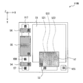
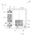
- FIG. 1A is a block diagram illustrating a configuration example of a function of the solid-state imaging device 101A according to the first embodiment of the present technology.
- the solid-state imaging device 101A is a so-called global shutter type back-illuminated image sensor such as a CMOS (Complementary Metal Oxide Semiconductor) image sensor.
- the solid-state imaging device 101A captures an image by receiving light from a subject, photoelectrically converting the light, and generating an image signal.
- CMOS Complementary Metal Oxide Semiconductor
- the global shutter method is a method of performing global exposure in which exposure is basically started simultaneously for all pixels and exposure is completed for all pixels simultaneously.
- all pixels are all pixels in a portion appearing in an image, and a dummy pixel or the like is excluded.
- a method of moving the global exposure area while performing global exposure in units of a plurality of rows (for example, several tens of rows) instead of all pixels simultaneously may be used. It is included in the global shutter system.
- the global shutter method also includes a method in which global exposure is performed on pixels in a predetermined area instead of all of the pixels in a portion appearing in an image.
- a back-illuminated image sensor is a photoelectric conversion unit such as a photodiode that receives light from a subject and converts it into an electric signal.
- a light-receiving surface on which light from the subject is incident and wiring such as a transistor that drives each pixel. Refers to an image sensor having a structure provided between the wiring layer and the wiring layer provided with.
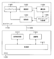
- the solid-state imaging device 101A includes, for example, a pixel array unit 111, a vertical drive unit 112, a column signal processing unit 113, a data storage unit 119, a horizontal drive unit 114, a system control unit 115, and a signal processing unit 118.
- the pixel array unit 111 is formed on the semiconductor layer 11 (described later). Peripheral circuits such as the vertical drive unit 112, the column signal processing unit 113, the data storage unit 119, the horizontal drive unit 114, the system control unit 115, and the signal processing unit 118 are, for example, on the same semiconductor layer 11 as the pixel array unit 111. It is formed.
- the pixel array unit 111 has a plurality of sensor pixels 110 including the photoelectric conversion unit 51 (described later) that generates and accumulates charges according to the amount of light incident from the subject. As shown in FIG. 1, the sensor pixels 110 are arranged in the horizontal direction (row direction) and the vertical direction (column direction). In the pixel array section 111, for each pixel row including the sensor pixels 110 arranged in one row in the row direction, a pixel driving line 116 is wired along the row direction, and is made up of the sensor pixels 110 arranged in one column in the column direction. For each pixel column, a vertical signal line (VSL) 117 is wired along the column direction.
- VSL vertical signal line
- the vertical drive unit 112 includes a shift register, an address decoder, and the like.
- the vertical drive unit 112 supplies all of the plurality of sensor pixels 110 in the pixel array unit 111 simultaneously by supplying signals and the like to the plurality of sensor pixels 110 via the plurality of pixel drive lines 116, or Drive by row.
- the vertical drive unit 112 has two scanning systems, for example, a reading scanning system and a sweeping scanning system.
- the readout scanning system selectively scans the unit pixels of the pixel array unit 111 in row units in order to read out signals from the unit pixels.
- the sweep-out scanning system performs a sweep-out scan on the readout row on which the readout scan is performed by the readout scan system ahead of the readout scan by a time corresponding to the shutter speed.
- Unnecessary charges are swept out from the photoelectric conversion units 51 of the unit pixels in the readout row by the sweeping scan by the sweeping scanning system. This is called a reset. Then, a so-called electronic shutter operation is performed by sweeping out unnecessary charges by the sweep-out scanning system, that is, by resetting.
- the electronic shutter operation refers to an operation of discarding the photoelectric charge of the photoelectric conversion unit 51 and newly starting exposure, that is, an operation of newly starting accumulation of the photoelectric charge.
- the signal read out by the readout operation by the readout scanning system corresponds to the amount of light incident after the immediately preceding readout operation or the electronic shutter operation.
- the period from the read timing by the immediately preceding read operation or the sweep timing by the electronic shutter operation to the read timing by the current read operation is the photocharge accumulation time in the unit pixel, that is, the exposure time.
- the signal output from each unit pixel of the pixel row selectively scanned by the vertical driving unit 112 is supplied to the column signal processing unit 113 through each of the vertical signal lines 117.
- the column signal processing unit 113 performs predetermined signal processing on a signal output from each unit pixel of the selected row through the vertical signal line 117 for each pixel column of the pixel array unit 111, and performs pixel processing after the signal processing. Is temporarily held.
- the column signal processing unit 113 includes, for example, a shift register and an address decoder, and performs noise removal processing, correlated double sampling processing, A / D (Analog / Digital) conversion A / D conversion processing of analog pixel signals. And so on to generate a digital pixel signal.
- the column signal processing unit 113 supplies the generated pixel signal to the signal processing unit 118.
- the horizontal drive unit 114 is configured by a shift register, an address decoder, and the like, and sequentially selects unit circuits corresponding to the pixel columns of the column signal processing unit 113. By the selective scanning by the horizontal driving unit 114, the pixel signals subjected to the signal processing for each unit circuit in the column signal processing unit 113 are sequentially output to the signal processing unit 118.
- the system control unit 115 includes a timing generator that generates various timing signals.
- the system control unit 115 controls the driving of the vertical driving unit 112, the column signal processing unit 113, and the horizontal driving unit 114 based on the timing signal generated by the timing generator.
- the signal processing unit 118 performs signal processing such as arithmetic processing on the pixel signals supplied from the column signal processing unit 113 while temporarily storing data in the data storage unit 119 as necessary, and performs processing for each pixel signal. Is output.
- the data storage section 119 temporarily stores data necessary for the signal processing in the signal processing in the signal processing section 118.
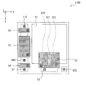
- FIG. 1B is a block diagram illustrating a configuration example of functions of a solid-state imaging device 101B as a first modification example according to the first embodiment of the present technology.
- FIG. 1C is a block diagram illustrating a configuration example of a function of a solid-state imaging device 101C as a second modification example according to the first embodiment of the present technology.
- a data storage unit 119 is disposed between the column signal processing unit 113 and the horizontal driving unit 114, and a pixel signal output from the column signal processing unit 113 stores data in the data storage unit 119.
- the signal is supplied to the signal processing unit 118 via the control unit.
- a data storage unit 119 and a signal processing unit 118 are arranged in parallel between the column signal processing unit 113 and the horizontal driving unit 114.
- the column signal processing unit 113 performs A / D conversion for converting an analog pixel signal into a digital pixel signal for each column of the pixel array unit 111 or for each of a plurality of columns of the pixel array unit 111. I have.
- FIG. 2 illustrates an example of a circuit configuration of one sensor pixel 110 of the plurality of sensor pixels 110 included in the pixel array unit 111.
- the sensor pixels 110 in the pixel array unit 111 include a photoelectric conversion unit (PD) 51, a transfer transistor (TG) 52, a charge-voltage conversion unit (FD) 53, a reset transistor (RST) 54, and an amplification.
- a transistor (AMP) 55 and a selection transistor (SEL) 56 are included.
- TG 52, RST 54, AMP 55, and SEL 56 are all N-type MOS transistors.
- Drive signals S52, S54 and S56 are supplied to the respective gate electrodes of the TG 52, RST 54, AMP 55 and SEL 56 by the vertical drive unit 112 and the horizontal drive unit 114 based on the drive control of the system control unit 115, respectively.
- the drive signals S52, S54, and S56 are pulse signals in which a high-level state becomes an active state (ON state) and a low-level state becomes an inactive state (OFF state).
- bringing the drive signal into the active state is also referred to as turning on the drive signal
- bringing the drive signal into the inactive state is also referred to as turning off the drive signal.
- the PD 51 is a photoelectric conversion element composed of, for example, a photodiode of a PN junction, and is configured to receive light from a subject, generate a charge corresponding to the amount of received light by photoelectric conversion, and accumulate the charge.
- the TG 52 is connected between the PD 51 and the FD 53, and is configured to transfer charges accumulated in the PD 51 to the FD 53 in accordance with a drive signal S52 applied to the gate electrode of the TG 52.
- the TG 52 is a specific example corresponding to the “transfer unit” of the present disclosure.
- the RST 54 has a drain connected to the power supply VDD and a source connected to the FD 53.
- the RST 54 initializes, that is, resets, the FD 53 according to the drive signal S54 applied to the gate electrode. For example, when the drive signal S58 turns on and the RST 58 turns on, the potential of the FD 53 is reset to the voltage level of the power supply VDD. That is, the FD 53 is initialized.
- the FD 53 is a floating diffusion region that converts the electric charge transferred from the PD 51 via the TG 52 into an electric signal (for example, a voltage signal) and outputs the electric signal.
- the FD 53 is connected to the RST 54 and the vertical signal line VSL via the AMP 55 and the SEL 56.
- FIG. 3 illustrates an example of a planar configuration of one sensor pixel 110 of the plurality of sensor pixels 110 included in the pixel array unit 111.
- FIG. 4A shows an example of a cross-sectional configuration of one sensor pixel 110, which corresponds to a cross-section taken along the line IV-IV shown in FIG.
- an XZ section along the X-axis direction is shown between a position P1 and a position P2, and the other is an YZ section along the Y-axis direction.
- the PD 51 occupies the central area of the sensor pixel 110, and RST 54, VDD, AMP 55, SEL 56, FD 57, VSS and VSL 117 are provided in the peripheral area. ing.
- the TG 52 and the FD 53 are provided at positions overlapping the PD 51 in the Z-axis direction (also referred to as a thickness direction or a depth direction).
- the FD 57 is connected to the FD 53 by a metal layer.
- VSS is a ground terminal, which is normally set to 0V.
- the sensor pixel 110 includes a semiconductor layer 11 formed of a semiconductor material such as Si (silicon), a PD 51, and a TG 52 as a transfer unit. . Further, an insulating layer 13 made of an oxide or the like is provided between the TG 52, the semiconductor layer 11, and the PD 51.
- the semiconductor layer 11 includes a front surface 11S1 and a back surface 11S2 opposite to the front surface 11S1.
- the semiconductor layer 11 may be provided with a light shielding portion 12 so as to surround the PD 51.
- TG 52 includes a trench gate 521 and a trench gate 522.
- the TG 52 transfers the charge generated and accumulated in the PD 51 from the PD 51 to the same transfer destination, that is, the FD 53 via the trench gate 521 and the trench gate 522, respectively.
- the trench gate 521 and the trench gate 522 extend from the front surface 11S1 of the semiconductor layer 11 to the back surface 11S2 to the PD 51, respectively.
- the trench gate 521 has a length L521 from the surface 11S1 to the PD 51.
- the trench gate 522 has a length L522 shorter than the length L521 from the surface 11S1 to the PD 51 (L521> L522).
- the diameter D521 of the trench gate 521 and the diameter D522 of the trench gate 522 are smaller as going from the front surface 11S1 to the back surface 11S2. Further, the maximum value of the diameter D521 of the trench gate 521 is larger than the maximum value of the diameter D522 of the trench gate 522. In the example shown in FIG. 4A, the diameter D521 of the trench gate 521 and the diameter D522 of the trench gate 522 are both maximum at the uppermost part.
- the sensor pixel 110 turns on the drive signal S52 to the TG 52 based on the drive control of the system control unit 115 when reading out the charge generated and accumulated in the PD 51 that has received light from the subject. As a result, the charge accumulated in the PD 51 is transferred from the PD 51 to the FD 53 via the trench gate 521 and the trench gate 522.
- the potential in the depth direction (Z-axis direction) of the PD 51 gradually increases from a deeper position, that is, a position closer to the back surface 11S2, to a shallower position, that is, a position closer to the front surface 11S1. have.
- a potential dip may occur in a part of the PD 51 in the depth direction.
- a potential dip is a location having a lower potential compared to the potential immediately above and below it.
- the potential gradient in the depth direction becomes gentle, and a potential dip tends to occur.
- the potential state in the thickness direction (Z-axis direction) of the PD 51 is, for example, the state shown in FIG. 4B.
- FIG. 4B is a schematic diagram illustrating a potential state in the depth direction (Z-axis direction) of the PD 51 when it is assumed that the TG 52 has only one trench gate 521.
- the TG 52 has the relatively long trench gate 521 and the relatively short trench gate 522.
- the potential of the PD 51 increases the modulating force received from the TG 52. Will be done.
- the potential state in the thickness direction (Z-axis direction) of the PD 51 becomes, for example, the state shown in FIG. 4C, and the potential dip existing in a part of the depth direction is eliminated.
- FIG. 4C is a schematic diagram illustrating a potential state in the depth direction (Z-axis direction) of the PD 51, and corresponds to the cross section of FIG.
- the TG 52 that transfers charges from the PD 51 includes the trench gate 521 having the length L521 and the trench gate 522 having the length L522 shorter than the length L521. And so on. For this reason, even if an unintended potential dip exists in the PD 51 while the TG 52 is off or an unintended potential dip is generated in the PD 51 for the purpose of increasing the saturation charge, the TG 52 is turned on. In the state described above, the potential dip can be eliminated.
- each of the diameter D521 of the trench gate 521 and the diameter D522 of the trench gate 522 becomes thinner from the front surface 11S1 to the back surface 11S2. Further, the maximum value of the diameter D521 of the trench gate 521 is larger than the maximum value of the diameter D522 of the trench gate 522. Therefore, the structure is advantageous for accurately forming the trench gate 521 having the larger length L521 and the trench gate 522 having the length L522 shorter than the length L521.
- FIG. 5 is a plan view illustrating a sensor pixel 110A as a third modification of the first embodiment.
- FIG. 5 corresponds to FIG. 3 of the first embodiment.
- the sensor pixel 110A according to the present modification is configured such that the FD 53 that is the charge transfer destination is located between the trench gate 521 and the trench gate 522. Except for this point, the other configuration is substantially the same as that of the sensor pixel 110 according to the first embodiment.
- the FD 53 that is the transfer destination is located between the trench gate 521 and the trench gate 522 as compared with the sensor pixel 110 according to the first embodiment. It is arranged.
- the back bias effect is eliminated in the portion between the trench gate 521 and the trench gate 522, and the modulation force received from the TG 52 becomes the highest. Therefore, the transferred charge is necessarily transferred to the surface 11S1 through the space between the trench gate 521 and the trench gate 522.
- the presence of the FD 53, which is the transfer destination of the charge, near the surface 11S improves the transfer efficiency of the charge from the PD 51 to the FD 53.
- FIG. 6 is a plan view illustrating a sensor pixel 110B as a fourth modification of the first embodiment.
- FIG. 6 corresponds to FIG. 3 of the first embodiment.
- the sensor pixel 110B is such that the TG 52 further includes a trench gate 523 as a third trench gate in addition to the trench gate 521 and the trench gate 522. .
- Each of the trench gates 521 to 523 has a substantially square cross section along the XY plane. Further, in the XY plane, the distance between the trench gate 522 and the FD 53 that is the transfer destination is shorter than the distance between the trench gate 521 and the FD 53 and shorter than the distance between the trench gate 523 and the FD 53. Except for these points, the other configuration is substantially the same as that of the sensor pixel 110 according to the first embodiment.
- the trench gate 523 is further provided, so that the number of the trench gates is larger than that of the sensor pixel 110. For this reason, a modulating force can be exerted on the potential of a region of the PD 51 located further away from the TG 52 in the horizontal plane (XY plane). As a result, charge transfer from the PD 51 to the FD 53 can be performed more smoothly.
- FIG. 7 is a plan view illustrating a sensor pixel 110C as a fifth modification of the first embodiment.
- FIG. 7 corresponds to FIG. 3 of the first embodiment.
- the sensor pixel 110C is such that the TG 52 further includes a trench gate 523 as a third trench gate in addition to the trench gate 521 and the trench gate 522. .
- Each of the trench gates 521 to 523 has a substantially square cross section along the XY plane. Further, in the XY plane, the distance between the trench gate 521 and the FD 53 that is the transfer destination is longer than the distance between the trench gate 522 and the FD 53 and longer than the distance between the trench gate 523 and the FD 53. Except for these points, the other configuration is substantially the same as that of the sensor pixel 110 according to the first embodiment.
- the trench gate 523 is further provided, so that the number of the trench gates is larger than that of the sensor pixel 110. For this reason, a modulating force can be exerted on the potential of a region of the PD 51 located further away from the TG 52 in the horizontal plane (XY plane). As a result, charge transfer from the PD 51 to the FD 53 can be performed more smoothly.
- two of the three trench gates are arranged in the vicinity of the FD 53 that is the charge transfer destination. Therefore, compared with the sensor pixel 110B as the fourth modification of the first embodiment shown in FIG.
- the charge of the PD 51 can be more efficiently transferred to the FD 53. This is because a favorable transfer path that can transfer the charge of the PD 51 more efficiently, that is, a region portion sandwiched between the trench gate 522 and the trench gate 523 is arranged near the FD 53.
- FIG. 8 is a plan view illustrating a sensor pixel 110D as a sixth modification of the first embodiment.
- FIG. 8 corresponds to FIG. 3 of the first embodiment.
- each of the trench gates 521 and 522 has a substantially square cross section along the XY plane. Except for this point, the other configuration is substantially the same as that of the sensor pixel 110 according to the first embodiment.
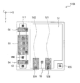
- FIG. 9A illustrates a planar configuration example of the sensor pixel 210 according to the second embodiment of the present technology.
- FIG. 9B shows a circuit configuration example of the sensor pixel 210.
- VDD2 is further provided in addition to the FD53 as a charge transfer destination of the PD51, and a discharge transistor (OFG) 58 is further provided between the PD51 and VDD2. . Except for these points, the other configuration is substantially the same as that of the sensor pixel 110 according to the first embodiment.
- the OFG 58 has a drain connected to the power supply VDD2 and a source connected to a wiring connecting the TG 52 and the PD 51.
- the OFG 58 initializes, that is, resets the PD 51 according to the drive signal S58 applied to the gate electrode. Resetting the PD 51 means that the PD 51 is depleted.
- the OFG 58 forms an overflow path between the TG 52 and the power supply VDD2, and discharges the charge overflowing from the PD 51 to the power supply VDD2. As described above, in the sensor pixel 210 of the present embodiment, the OFG 58 can directly reset the PD 51, and an FD holding global shutter can be realized.
- a plurality of trench gates having different depths that is, a trench gate 581 and a trench gate 582 are provided also in the OFG 58.
- the length of the trench gate 581 and the length of the trench gate 582 are different.
- the transfer failure at the time of discharging the charges overflowing from the PD 51 to the power supply VDD2. Can be prevented.
- FIG. 10A illustrates a planar configuration example of a sensor pixel 310 according to the third embodiment of the present technology.
- FIG. 10B shows a circuit configuration example of the sensor pixel 310.
- the sensor pixel 310 of the present embodiment is such that a charge holding unit (MEM) 59 is further provided between the PD 51 and the FD 53. Accordingly, a first transfer transistor (TG) 52A and a second transfer transistor (TG) 52B are provided instead of the TG 52.
- the TG 52A is arranged between the PD 51 and the MEM 59, and the TG 52B is arranged between the MEM 59 and the FD 53. Except for these points, the other configuration is substantially the same as that of the sensor pixel 210 according to the second embodiment.
- the charge from the PD 51 is transferred to the MEM 59, and a memory-holding global shutter can be realized.
- the drive signal S52A applied to the gate electrode of the TG 52A is turned on, and when the TG 52A is turned on, the charge accumulated in the PD 51 is transferred to the MEM 59 via the TG 52A.
- the MEM 59 is an area for temporarily holding the charge accumulated in the PD 51 in order to realize the global shutter function.
- the TG 52B transfers the electric charge held in the MEM 59 to the FD 53 in accordance with the drive signal S52B applied to the gate electrode of the TG 52B.
- the drive signal S52 when the drive signal S52 is turned off, the TG 52A is turned off, the drive signal S52B is turned on, and the TG 52B is turned on, the electric charge held in the MEM 59 is transferred to the FD 53 via the TG 52B.
- MEM 59 has trench gates 591 and 592 having different depths. For this reason, a transfer failure at the time of transferring the charge in the PD 51 to the MEM 59 can be prevented.
- FIG. 11A illustrates a planar configuration example of a sensor pixel 410 according to the fourth embodiment of the present technology.
- FIG. 11B shows an example of a circuit configuration of the sensor pixel 410.
- FIG. 11C shows a cross-sectional configuration example of the sensor pixel 410.
- the transfer unit is configured so that the first transfer transistor (TG) 52A and the second transfer transistor (TG) can be driven independently of each other.
- TG 52A includes trench gate TG 521
- TG 52B includes trench gate TG 522. Except for these points, the other configuration is substantially the same as that of the sensor pixel 110 according to the first embodiment. Therefore, in the sensor pixel 410, similarly to the sensor pixel 110, the length L522 of the trench gate 522 is shorter than the length L521 of the trench gate 521 (L521> L522).
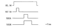
- the TG 52A and the TG 52B can be driven independently, so that the ON / OFF driving timing of the TG 52A and the ON / OFF driving timing of the TG 52B can be freely selected. Therefore, as shown in FIG. 12A, for example, after the TG 52A and the TG 52B are simultaneously activated, that is, simultaneously from the off state to the on state, the TG 52A is lowered before the TG 52B (from the on state to the off state). )be able to.
- the modulating force that the potential of the PD 51 receives from the TG 52 increases along the Z-axis direction from the back surface 11S2 to the front surface 11S1.
- the potential dip in the PD 51 is more effectively eliminated as compared with the case in which one TG 52 is provided with two trench gates TG 521 and TG 522 as in the sensor pixel 110 according to the first embodiment. can do.
- the ON / OFF drive timing of the TG 52A and the ON / OFF drive timing of the TG 52B are not limited to the case shown in FIG. 12A, and may be, for example, as shown in FIG. 12B.
- FIG. 12B shows an example in which the TG 52A is activated before the TG 52B and the TG 52A is activated before the TG 52B. That is, in the sensor pixel 410 of the present embodiment, the on-state period in the TG 52A and the on-state period in the TG 52B may partially overlap, and the TG 52A may fall before the TG 52B. Alternatively, as shown in FIG.
- the timing to complete the fall of TG 52A is the time when the fall of TG 52B is completed. It suffices that it comes before the timing to perform. That is, by changing the gradient of the speed of switching from the ON state to the OFF state, the timing of the completion of the switching from the ON state to the OFF state in the TG 52B is later than the timing of the completion of the switching from the ON state to the OFF state in the TG 52A. You may. The rounding of the pulse shown in FIG.
- FIGS. 12A to 12C are time charts showing the waveforms of the respective drive signals supplied to the RST 54, SEL 56, TG 52A and TG 52B.
- FIG. 13A is a plan view illustrating a sensor pixel 410A as a first modification of the fourth embodiment.
- FIG. 13A corresponds to FIG. 11A of the fourth embodiment.
- the sensor pixel 410A according to this modification has the FD 53 that is the transfer destination of the electric charge positioned between the trench gate 521 and the trench gate 522. Except for this point, the other configuration is substantially the same as that of the sensor pixel 410 according to the fourth embodiment.
- the FD 53 that is the transfer destination is located between the trench gate 521 and the trench gate 522, as compared with the sensor pixel 410 according to the fourth embodiment. It is arranged.
- the back bias effect is eliminated in the portion between the trench gate 521 and the trench gate 522, and the modulation force received from the TG 52A and TG 52B becomes the highest. Therefore, the transferred charge is necessarily transferred to the surface 11S1 through the space between the trench gate 521 and the trench gate 522.
- the presence of the FD 53, which is the transfer destination of the charge, near the surface 11S improves the transfer efficiency of the charge from the PD 51 to the FD 53.
- FIG. 13B is a plan view illustrating a sensor pixel 410B as a second modification of the fourth embodiment.
- FIG. 13B corresponds to FIG. 11A of the fourth embodiment.
- the TG 52A includes both the trench gate 521 and the trench gate 522.
- the TG 52B does not have a trench gate, and is located between the TG 52A and the FD 53 to which the charge is transferred. Except for this point, the other configuration is substantially the same as that of the sensor pixel 410 according to the fourth embodiment.
- FIG. 13C is a plan view illustrating a sensor pixel 410C as a third modification of the fourth embodiment.
- FIG. 13C corresponds to FIG. 11A of the fourth embodiment.
- the sensor pixel 410C according to the present modification further includes, as a transfer unit, a TG 52C that can be driven independently of the TG 52A and the TG 52B.
- TG 52A includes a trench gate 521
- TG 52B includes a trench gate 522
- TG 52C includes a trench gate 523.
- the other configuration is substantially the same as that of the sensor pixel 410 according to the fourth embodiment.
- the TG 52C is further provided, so that the charge transfer from the PD 51 in the horizontal plane (the XY plane) is performed more smoothly than in the sensor pixel 410. be able to. Therefore, for example, the saturation signal amount of the PD 51 can be easily increased.
- FIG. 13D is a plan view illustrating a sensor pixel 410D as a fourth modification of the fourth embodiment.
- FIG. 13D corresponds to FIG. 11A of the fourth embodiment.
- the TG 52C does not have a trench gate. Except for this point, the other configuration is substantially the same as that of the sensor pixel 410C as the third modified example of the fourth embodiment.
- FIG. 14 is a block diagram illustrating a configuration example of a camera 2000 as an electronic device to which the present technology is applied.
- the camera 2000 is an optical unit 2001 including a lens group, an imaging device (imaging device) 2002 to which the above-described solid-state imaging device 101 or the like (hereinafter, referred to as the solid-state imaging device 101 or the like) is applied, and a camera signal processing circuit.
- a DSP (Digital Signal Processor) circuit 2003 is provided.
- the camera 2000 also includes a frame memory 2004, a display unit 2005, a recording unit 2006, an operation unit 2007, and a power supply unit 2008.
- the DSP circuit 2003, the frame memory 2004, the display unit 2005, the recording unit 2006, the operation unit 2007, and the power supply unit 2008 are interconnected via a bus line 2009.
- the optical unit 2001 captures incident light (image light) from a subject and forms an image on the imaging surface of the imaging device 2002.
- the imaging device 2002 converts the amount of incident light formed on the imaging surface by the optical unit 2001 into an electric signal in pixel units and outputs the electric signal as a pixel signal.
- the display unit 2005 includes, for example, a panel-type display device such as a liquid crystal panel or an organic EL panel, and displays a moving image or a still image captured by the imaging device 2002.
- the recording unit 2006 records a moving image or a still image captured by the imaging device 2002 on a recording medium such as a hard disk or a semiconductor memory.
- the operation unit 2007 issues operation commands for various functions of the camera 2000 under user operation.
- the power supply unit 2008 appropriately supplies various power supplies serving as operation power supplies for the DSP circuit 2003, the frame memory 2004, the display unit 2005, the recording unit 2006, and the operation unit 2007 to these supply targets.
- the technology (the present technology) according to the present disclosure can be applied to various products.
- the technology according to the present disclosure is realized as a device mounted on any type of moving object such as an automobile, an electric vehicle, a hybrid electric vehicle, a motorcycle, a bicycle, a personal mobility, an airplane, a drone, a ship, and a robot. You may.
- FIG. 15 is a block diagram illustrating a schematic configuration example of a vehicle control system that is an example of a mobile object control system to which the technology according to the present disclosure can be applied.
- Vehicle control system 12000 includes a plurality of electronic control units connected via communication network 12001.
- the vehicle control system 12000 includes a drive system control unit 12010, a body system control unit 12020, an outside information detection unit 12030, an inside information detection unit 12040, and an integrated control unit 12050.
- a microcomputer 12051 As a functional configuration of the integrated control unit 12050, a microcomputer 12051, a sound image output unit 12052, a vehicle-mounted network I / F (Interface) 120 53 is shown.
- the drive system control unit 12010 controls the operation of the device related to the drive system of the vehicle according to various programs.
- the drive system control unit 12010 includes a drive force generation device for generating a drive force of the vehicle such as an internal combustion engine or a drive motor, a drive force transmission mechanism for transmitting the drive force to the wheels, and a steering angle of the vehicle. It functions as a control mechanism such as a steering mechanism that adjusts and a braking device that generates a braking force of the vehicle.
- the body control unit 12020 controls the operation of various devices mounted on the vehicle body according to various programs.
- the body-related control unit 12020 functions as a keyless entry system, a smart key system, a power window device, or a control device for various lamps such as a head lamp, a back lamp, a brake lamp, a blinker, and a fog lamp.
- a radio wave or a signal of various switches transmitted from a portable device replacing the key can be input to the body control unit 12020.
- the body control unit 12020 receives the input of these radio waves or signals, and controls a door lock device, a power window device, a lamp, and the like of the vehicle.
- Out-of-vehicle information detection unit 12030 detects information external to the vehicle on which vehicle control system 12000 is mounted.
- an imaging unit 12031 is connected to the outside-of-vehicle information detection unit 12030.
- the out-of-vehicle information detection unit 12030 causes the imaging unit 12031 to capture an image outside the vehicle, and receives the captured image.
- the out-of-vehicle information detection unit 12030 may perform an object detection process or a distance detection process of a person, a vehicle, an obstacle, a sign, a character on a road surface, or the like based on the received image.
- the imaging unit 12031 is an optical sensor that receives light and outputs an electric signal according to the amount of received light.
- the imaging unit 12031 can output an electric signal as an image or can output the information as distance measurement information.
- the light received by the imaging unit 12031 may be visible light or non-visible light such as infrared light.
- the in-vehicle information detection unit 12040 detects information in the vehicle.
- the in-vehicle information detection unit 12040 is connected to, for example, a driver status detection unit 12041 that detects the status of the driver.
- the driver state detection unit 12041 includes, for example, a camera that captures an image of the driver, and the in-vehicle information detection unit 12040 determines the degree of driver fatigue or concentration based on the detection information input from the driver state detection unit 12041. The calculation may be performed, or it may be determined whether the driver has fallen asleep.
- the microcomputer 12051 calculates a control target value of the driving force generation device, the steering mechanism or the braking device based on the information on the inside and outside of the vehicle acquired by the outside information detection unit 12030 or the inside information detection unit 12040, and the drive system control unit A control command can be output to 12010.
- the microcomputer 12051 implements an ADAS (Advanced Driver Assistance System) function including a vehicle collision avoidance or impact mitigation, a following operation based on an inter-vehicle distance, a vehicle speed maintaining operation, a vehicle collision warning, or a vehicle lane departure warning. Cooperative control for the purpose.
- ADAS Advanced Driver Assistance System
- the microcomputer 12051 controls the driving force generation device, the steering mechanism, the braking device, and the like based on the information on the surroundings of the vehicle acquired by the outside information detection unit 12030 or the inside information detection unit 12040, and thereby, It is possible to perform cooperative control for automatic driving or the like in which the vehicle travels autonomously without depending on the operation.
- the microcomputer 12051 can output a control command to the body system control unit 12020 based on information on the outside of the vehicle acquired by the outside information detection unit 12030.
- the microcomputer 12051 controls the headlamp according to the position of the preceding vehicle or the oncoming vehicle detected by the outside information detection unit 12030, and performs cooperative control for the purpose of preventing glare such as switching a high beam to a low beam. It can be carried out.
- the sound image output unit 12052 transmits at least one of a sound signal and an image signal to an output device capable of visually or audibly notifying a passenger of the vehicle or the outside of the vehicle of information.
- an audio speaker 12061, a display unit 12062, and an instrument panel 12063 are illustrated as output devices.
- the display unit 12062 may include, for example, at least one of an on-board display and a head-up display.
- FIG. 16 is a diagram illustrating an example of an installation position of the imaging unit 12031.
- the imaging unit 12031 includes imaging units 12101, 12102, 12103, 12104, and 12105.
- the imaging units 12101, 12102, 12103, 12104, and 12105 are provided, for example, at positions such as a front nose, a side mirror, a rear bumper, a back door, and an upper part of a windshield in the vehicle interior of the vehicle 12100.
- the imaging unit 12101 provided on the front nose and the imaging unit 12105 provided above the windshield in the passenger compartment mainly acquire an image in front of the vehicle 12100.
- the imaging units 12102 and 12103 provided in the side mirror mainly acquire images of the side of the vehicle 12100.
- the imaging unit 12104 provided in the rear bumper or the back door mainly acquires an image behind the vehicle 12100.
- the imaging unit 12105 provided above the windshield in the passenger compartment is mainly used for detecting a preceding vehicle, a pedestrian, an obstacle, a traffic light, a traffic sign, a lane, and the like.
- FIG. 22 shows an example of the imaging range of the imaging units 12101 to 12104.
- the imaging range 12111 indicates the imaging range of the imaging unit 12101 provided on the front nose
- the imaging ranges 12112 and 12113 indicate the imaging ranges of the imaging units 12102 and 12103 provided on the side mirrors, respectively
- the imaging range 12114 indicates 14 shows an imaging range of an imaging unit 12104 provided in a rear bumper or a back door. For example, by overlaying image data captured by the imaging units 12101 to 12104, an overhead image of the vehicle 12100 viewed from above can be obtained.
- At least one of the imaging units 12101 to 12104 may have a function of acquiring distance information.
- at least one of the imaging units 12101 to 12104 may be a stereo camera including a plurality of imaging elements or an imaging element having pixels for detecting a phase difference.
- the microcomputer 12051 calculates a distance to each three-dimensional object in the imaging ranges 12111 to 12114 and a temporal change of the distance (relative speed with respect to the vehicle 12100).
- a distance to each three-dimensional object in the imaging ranges 12111 to 12114 and a temporal change of the distance (relative speed with respect to the vehicle 12100).
- microcomputer 12051 can set an inter-vehicle distance to be secured before the preceding vehicle and perform automatic brake control (including follow-up stop control), automatic acceleration control (including follow-up start control), and the like. In this way, it is possible to perform cooperative control for automatic driving or the like in which the vehicle travels autonomously without depending on the operation of the driver.
- the microcomputer 12051 converts the three-dimensional object data relating to the three-dimensional object into other three-dimensional objects such as a motorcycle, a normal vehicle, a large vehicle, a pedestrian, a telephone pole, and the like based on the distance information obtained from the imaging units 12101 to 12104. It can be classified and extracted and used for automatic avoidance of obstacles. For example, the microcomputer 12051 distinguishes obstacles around the vehicle 12100 into obstacles that are visible to the driver of the vehicle 12100 and obstacles that are difficult to see. Then, the microcomputer 12051 determines a collision risk indicating a risk of collision with each obstacle, and when the collision risk is equal to or more than the set value and there is a possibility of collision, via the audio speaker 12061 or the display unit 12062. By outputting an alarm to the driver through forced driving and avoidance steering via the drive system control unit 12010, driving assistance for collision avoidance can be performed.
- driving assistance for collision avoidance can be performed.
- At least one of the imaging units 12101 to 12104 may be an infrared camera that detects infrared light.
- the microcomputer 12051 can recognize a pedestrian by determining whether or not a pedestrian exists in the captured images of the imaging units 12101 to 12104. The recognition of such a pedestrian is performed by, for example, extracting a feature point in an image captured by the imaging units 12101 to 12104 as an infrared camera, and performing a pattern matching process on a series of feature points indicating the outline of the object to determine whether the object is a pedestrian.
- the audio image output unit 12052 outputs a rectangular outline to the recognized pedestrian for emphasis.
- the display unit 12062 is controlled so that is superimposed.
- the sound image output unit 12052 may control the display unit 12062 to display an icon or the like indicating a pedestrian at a desired position.
- the technology according to the present disclosure can be applied to the imaging unit 12031 among the configurations described above.
- the solid-state imaging device 101A or the like illustrated in FIG. 1 or the like can be applied to the imaging unit 12031.
- Example of application to endoscopic surgery system The technology (the present technology) according to the present disclosure can be applied to various products.
- the technology according to the present disclosure may be applied to an endoscopic surgery system.
- FIG. 17 is a diagram illustrating an example of a schematic configuration of an endoscopic surgery system to which the technology (the present technology) according to the present disclosure may be applied.
- FIG. 17 shows a situation in which an operator (doctor) 11131 is performing an operation on a patient 11132 on a patient bed 11133 using the endoscopic surgery system 11000.
- the endoscopic surgery system 11000 includes an endoscope 11100, other surgical tools 11110 such as an insufflation tube 11111 and an energy treatment tool 11112, and a support arm device 11120 that supports the endoscope 11100.
- a cart 11200 on which various devices for endoscopic surgery are mounted.
- the endoscope 11100 includes a lens barrel 11101 having a predetermined length from the distal end inserted into the body cavity of the patient 11132, and a camera head 11102 connected to the proximal end of the lens barrel 11101.
- the endoscope 11100 which is configured as a so-called rigid endoscope having a hard lens barrel 11101 is illustrated.
- the endoscope 11100 may be configured as a so-called flexible endoscope having a soft lens barrel. Good.
- An opening in which an objective lens is fitted is provided at the tip of the lens barrel 11101.
- a light source device 11203 is connected to the endoscope 11100, and light generated by the light source device 11203 is guided to the distal end of the lens barrel by a light guide that extends inside the lens barrel 11101, and the objective The light is radiated toward the observation target in the body cavity of the patient 11132 via the lens.
- the endoscope 11100 may be a direct view scope, a perspective view scope, or a side view scope.
- An optical system and an image sensor are provided inside the camera head 11102, and the reflected light (observation light) from the observation target is focused on the image sensor by the optical system.
- the observation light is photoelectrically converted by the imaging element, and an electric signal corresponding to the observation light, that is, an image signal corresponding to the observation image is generated.
- the image signal is transmitted to a camera control unit (CCU: ⁇ Camera ⁇ Control ⁇ Unit) 11201 as RAW data.
- the $ CCU 11201 is configured by a CPU (Central Processing Unit), a GPU (Graphics Processing Unit), and the like, and controls the operations of the endoscope 11100 and the display device 11202 overall. Further, the CCU 11201 receives an image signal from the camera head 11102, and performs various image processing on the image signal for displaying an image based on the image signal, such as a development process (demosaicing process).
- a development process demosaicing process
- the display device 11202 displays an image based on an image signal on which image processing has been performed by the CCU 11201 under the control of the CCU 11201.
- the light source device 11203 includes a light source such as an LED (Light Emitting Diode), for example, and supplies the endoscope 11100 with irradiation light when imaging an operation part or the like.
- a light source such as an LED (Light Emitting Diode), for example, and supplies the endoscope 11100 with irradiation light when imaging an operation part or the like.
- the input device 11204 is an input interface for the endoscopic surgery system 11000.
- the user can input various information and input instructions to the endoscopic surgery system 11000 via the input device 11204.
- the user inputs an instruction or the like to change imaging conditions (type of irradiation light, magnification, focal length, and the like) by the endoscope 11100.
- the treatment instrument control device 11205 controls the driving of the energy treatment instrument 11112 for cauterizing, incising a tissue, sealing a blood vessel, and the like.
- the insufflation device 11206 is used to inflate the body cavity of the patient 11132 for the purpose of securing the visual field by the endoscope 11100 and securing the working space of the operator.
- the recorder 11207 is a device that can record various types of information related to surgery.
- the printer 11208 is a device capable of printing various types of information on surgery in various formats such as text, images, and graphs.
- the light source device 11203 that supplies the endoscope 11100 with irradiation light at the time of imaging the operation site can be configured by, for example, a white light source including an LED, a laser light source, or a combination thereof.
- a white light source is configured by a combination of the RGB laser light sources
- the output intensity and output timing of each color (each wavelength) can be controlled with high accuracy, so that the light source device 11203 adjusts the white balance of the captured image. It can be carried out.
- the laser light from each of the RGB laser light sources is radiated to the observation target in a time-division manner, and the driving of the image pickup device of the camera head 11102 is controlled in synchronization with the irradiation timing. It is also possible to capture the image obtained in a time-division manner. According to this method, a color image can be obtained without providing a color filter in the image sensor.
- the driving of the light source device 11203 may be controlled so as to change the intensity of output light at predetermined time intervals.
- the driving of the image sensor of the camera head 11102 in synchronization with the timing of the change of the light intensity, an image is acquired in a time-division manner, and the image is synthesized, so that a high dynamic image without so-called blackout and whiteout is obtained. An image of the range can be generated.
- the light source device 11203 may be configured to be able to supply light in a predetermined wavelength band corresponding to special light observation.
- the special light observation for example, the wavelength dependence of light absorption in body tissue is used to irradiate light of a narrower band compared to irradiation light (ie, white light) at the time of normal observation, so that the surface of the mucous membrane is exposed.
- a so-called narrow-band light observation (Narrow / Band / Imaging) for imaging a predetermined tissue such as a blood vessel with high contrast is performed.
- fluorescence observation in which an image is obtained by fluorescence generated by irradiating excitation light may be performed.
- body tissue is irradiated with excitation light to observe fluorescence from the body tissue (autofluorescence observation), or a reagent such as indocyanine green (ICG) is locally injected into the body tissue and Irradiation with excitation light corresponding to the fluorescence wavelength of the reagent can be performed to obtain a fluorescence image.
- the light source device 11203 can be configured to be able to supply narrowband light and / or excitation light corresponding to such special light observation.
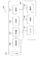
- FIG. 18 is a block diagram showing an example of a functional configuration of the camera head 11102 and the CCU 11201 shown in FIG.
- the camera head 11102 includes a lens unit 11401, an imaging unit 11402, a driving unit 11403, a communication unit 11404, and a camera head control unit 11405.
- the CCU 11201 includes a communication unit 11411, an image processing unit 11412, and a control unit 11413.
- the camera head 11102 and the CCU 11201 are communicably connected to each other by a transmission cable 11400.
- the lens unit 11401 is an optical system provided at a connection with the lens barrel 11101. Observation light taken in from the tip of the lens barrel 11101 is guided to the camera head 11102, and enters the lens unit 11401.
- the lens unit 11401 is configured by combining a plurality of lenses including a zoom lens and a focus lens.
- the imaging unit 11402 includes an imaging element.
- the number of imaging elements constituting the imaging unit 11402 may be one (so-called single-panel type) or plural (so-called multi-panel type).
- an image signal corresponding to each of RGB may be generated by each imaging element, and a color image may be obtained by combining the image signals.
- the imaging unit 11402 may be configured to include a pair of imaging elements for acquiring right-eye and left-eye image signals corresponding to 3D (Dimensional) display. By performing the 3D display, the operator 11131 can more accurately grasp the depth of the living tissue in the operative part.
- a plurality of lens units 11401 may be provided for each imaging element.
- the imaging unit 11402 does not necessarily have to be provided in the camera head 11102.
- the imaging unit 11402 may be provided inside the lens barrel 11101 immediately after the objective lens.
- the drive unit 11403 is configured by an actuator, and moves the zoom lens and the focus lens of the lens unit 11401 by a predetermined distance along the optical axis under the control of the camera head control unit 11405.
- the magnification and the focus of the image captured by the imaging unit 11402 can be appropriately adjusted.
- the communication unit 11404 is configured by a communication device for transmitting and receiving various information to and from the CCU 11201.
- the communication unit 11404 transmits the image signal obtained from the imaging unit 11402 as RAW data to the CCU 11201 via the transmission cable 11400.
- the communication unit 11404 receives a control signal for controlling driving of the camera head 11102 from the CCU 11201 and supplies the control signal to the camera head control unit 11405.
- the control signal includes, for example, information indicating that the frame rate of the captured image is specified, information that specifies the exposure value at the time of imaging, and / or information that specifies the magnification and focus of the captured image. Contains information about the condition.
- imaging conditions such as the frame rate, the exposure value, the magnification, and the focus may be appropriately designated by the user, or may be automatically set by the control unit 11413 of the CCU 11201 based on the acquired image signal. Good.
- a so-called AE (Auto Exposure) function, an AF (Auto Focus) function, and an AWB (Auto White Balance) function are mounted on the endoscope 11100.
- the camera head control unit 11405 controls the driving of the camera head 11102 based on the control signal from the CCU 11201 received via the communication unit 11404.
- the communication unit 11411 is configured by a communication device for transmitting and receiving various information to and from the camera head 11102.
- the communication unit 11411 receives an image signal transmitted from the camera head 11102 via the transmission cable 11400.
- the communication unit 11411 transmits a control signal for controlling driving of the camera head 11102 to the camera head 11102.
- the image signal and the control signal can be transmitted by electric communication, optical communication, or the like.
- the image processing unit 11412 performs various types of image processing on an image signal that is RAW data transmitted from the camera head 11102.
- the control unit 11413 performs various kinds of control related to imaging of the operation section and the like by the endoscope 11100 and display of a captured image obtained by imaging the operation section and the like. For example, the control unit 11413 generates a control signal for controlling driving of the camera head 11102.
- control unit 11413 causes the display device 11202 to display a captured image showing the operative part or the like based on the image signal subjected to the image processing by the image processing unit 11412.
- the control unit 11413 may recognize various objects in the captured image using various image recognition techniques. For example, the control unit 11413 detects a shape, a color, or the like of an edge of an object included in the captured image, and thereby detects a surgical tool such as forceps, a specific living body site, bleeding, a mist when using the energy treatment tool 11112, and the like. Can be recognized.
- the control unit 11413 may use the recognition result to superimpose and display various types of surgery support information on the image of the operative site.
- the burden on the operator 11131 can be reduced, and the operator 11131 can reliably perform the operation.
- the transmission cable 11400 connecting the camera head 11102 and the CCU 11201 is an electric signal cable corresponding to electric signal communication, an optical fiber corresponding to optical communication, or a composite cable thereof.
- the communication is performed by wire using the transmission cable 11400, but the communication between the camera head 11102 and the CCU 11201 may be performed wirelessly.
- the technology according to the present disclosure may be applied to (the image processing unit 11412 of) the CCU 11201 among the configurations described above.
- the solid-state imaging device 101A in FIG. 1A can be applied to the imaging unit 10402.
- the endoscopic surgery system has been described as an example, but the technology according to the present disclosure may be applied to, for example, a microscopic surgery system or the like.
- a global shutter type backside illumination type image sensor has been described as an example, but the imaging device of the present disclosure is not limited to this, and may be another type of image sensor. . That is, the present disclosure is not limited to the global shutter type image sensor, but is also applicable to a rolling shutter type image sensor. Furthermore, the present disclosure is not limited to a backside illumination type image sensor, but is also applicable to a frontside illumination type image sensor. Further, the technology of the present disclosure is not limited to application to a CMOS image sensor, but is applicable to all XY address type solid-state imaging devices in which unit pixels are two-dimensionally arranged in a matrix.
- the imaging apparatus is not limited to an imaging apparatus that detects a light amount distribution of visible light and obtains an image, and obtains, as an image, a distribution of an incident amount of infrared rays, X-rays, or particles. It may be an imaging device.
- the imaging device of the present disclosure may be in the form of a module in which an imaging unit and a signal processing unit or an optical system are packaged together.
- the sensor pixel having two or three transfer transistors separated from each other as a transfer unit is illustrated, but the imaging device according to the present disclosure may have four or more transfer transistors as a transfer unit. It may be.
- a semiconductor layer including a front surface and a back surface opposite to the front surface, Embedded in the semiconductor layer, a photoelectric conversion unit that generates a charge according to the amount of received light by photoelectric conversion, A first trench gate and a second trench gate each extending from the front surface of the semiconductor layer toward the back surface to the photoelectric conversion unit, wherein the charge is transferred from the photoelectric conversion unit to the first trench gate.
- a transfer unit for transferring to the same transfer destination via the gate and the second trench gate, respectively.
- the first trench gate has a first length from the surface to the photoelectric conversion unit
- the imaging device, wherein the second trench gate has a second length shorter than the first length from the surface to the photoelectric conversion unit.
- the imaging device according to (1), wherein the transfer destination is a charge-voltage converter.
- the imaging device according to (1), wherein the transfer destination is a charge holding unit.
- the imaging device according to (1), wherein the transfer destination is a power supply.
- the imaging device according to (1), wherein the transfer destination is located between the first trench gate and the second trench gate.
- (6) In a plane parallel to the surface, The imaging device according to any one of (1) to (5), wherein a distance between the second trench gate and the transfer destination is shorter than a distance between the first trench gate and the transfer destination.
- the imaging device includes a first transistor and a second transistor configured to be independently drivable.
- the first transistor includes the first trench gate;
- the first transistor includes the first trench gate and the second trench gate;
- the imaging device according to (7), wherein the second transistor is located between the first transistor and the transfer destination.
- the transfer unit has one transistor, The one transistor includes the first trench gate, the second trench gate, and a third trench gate, In a plane parallel to the surface, a second distance between the second trench gate and the transfer destination is shorter than a first distance between the first trench gate and the transfer destination; The third distance between the trench gate and the transfer destination is shorter than the first distance.
- the transfer unit has one transistor, The one transistor includes the first trench gate, the second trench gate, and a third trench gate, In a plane parallel to the surface, a second distance between the second trench gate and the transfer destination is shorter than a first distance between the first trench gate and the transfer destination; The third distance between the trench gate and the transfer destination is longer than the second distance.
- An electronic device including an imaging device, The imaging device, A semiconductor layer including a front surface and a back surface opposite to the front surface, Embedded in the semiconductor layer, a photoelectric conversion unit that generates a charge according to the amount of received light by photoelectric conversion, A first trench gate and a second trench gate each extending from the front surface of the semiconductor layer toward the back surface to the photoelectric conversion unit, wherein the charge is transferred from the photoelectric conversion unit to the first trench gate.
- a transfer unit for transferring to the same transfer destination via the gate and the second trench gate, respectively.
- the first trench gate has a first length from the surface to the photoelectric conversion unit
- the electronic device, wherein the second trench gate has a second length shorter than the first length from the surface to the photoelectric conversion unit.
Landscapes
- Engineering & Computer Science (AREA)
- Physics & Mathematics (AREA)
- Power Engineering (AREA)
- Electromagnetism (AREA)
- Condensed Matter Physics & Semiconductors (AREA)
- General Physics & Mathematics (AREA)
- Computer Hardware Design (AREA)
- Microelectronics & Electronic Packaging (AREA)
- Multimedia (AREA)
- Signal Processing (AREA)
- Solid State Image Pick-Up Elements (AREA)
- Transforming Light Signals Into Electric Signals (AREA)
Abstract
電荷が光電変換部から転送先へ円滑に転送される撮像装置を提供する。この撮像装置は、表面と、その表面と反対側の裏面とを含む半導体層と、その半導体層に埋設され、受光量に応じた電荷を光電変換により生成する光電変換部と、半導体層の表面から裏面へ向けて光電変換部へ至るまでそれぞれ延在する第1のトレンチゲートおよび第2のトレンチゲートを含み、電荷を光電変換部から第1のトレンチゲートおよび第2のトレンチゲートをそれぞれ介して同一の転送先へ転送する転送部とを備える。第1のトレンチゲートは、表面から光電変換部へ至るまで第1の長さを有し、第2のトレンチゲートは、表面から光電変換部へ至るまで第1の長さよりも短い第2の長さを有する。
Description
本開示は、光電変換を行うことで撮像を行う撮像装置およびその撮像装置を備えた電子機器に関する。
これまでに、半導体層に設けられた光電変換部において生成される信号電荷を、その半導体層に埋設されたゲート電極によりフローティングディフュージョン(floating diffusion)へ転送するようにした固体撮像装置が提案されている(例えば、特許文献1参照)。
ところで、このような固体撮像装置では、電荷が光電変換部から転送先へ円滑に転送されることが望ましい。
したがって、動作信頼性に優れる撮像装置およびそのような撮像装置を備えた電子機器を提供することが望まれる。
本開示の一実施形態としての撮像装置は、表面と、その表面と反対側の裏面とを含む半導体層と、その半導体層に埋設され、受光量に応じた電荷を光電変換により生成する光電変換部と、半導体層の表面から裏面へ向けて光電変換部へ至るまでそれぞれ延在する第1のトレンチゲートおよび第2のトレンチゲートを含み、電荷を光電変換部から第1のトレンチゲートおよび第2のトレンチゲートをそれぞれ介して同一の転送先へ転送する転送部とを備える。第1のトレンチゲートは、表面から光電変換部へ至るまで第1の長さを有し、第2のトレンチゲートは、表面から光電変換部へ至るまで第1の長さよりも短い第2の長さを有する。
また、本開示の一実施形態としての電子機器は、上記撮像装置を備えたものである。
また、本開示の一実施形態としての電子機器は、上記撮像装置を備えたものである。
本開示の一実施形態としての撮像装置および電子機器では、上記の構成により、転送部がオフの状態において、光電変換部にポテンシャルディップが存在していたとしても、転送部がオンの状態ではそのポテンシャルディップが解消される。
本開示の一実施形態としての撮像装置および電子機器によれば、電荷が光電変換部から転送先へ円滑に転送され、優れた撮像性能を実現できる。
なお、本開示の効果はこれに限定されるものではなく、以下に記載のいずれの効果であってもよい。
なお、本開示の効果はこれに限定されるものではなく、以下に記載のいずれの効果であってもよい。
以下、本開示の実施の形態について図面を参照して詳細に説明する。なお、説明は以下の順序で行う。
1.第1の実施の形態
転送部における一の縦型トランジスタが互いに深さの異なる2つのトレンチゲートを有する固体撮像装置の例。
2.第1の実施の形態の変形例
3.第2の実施の形態
電荷の転送先としての電源と、排出トランジスタとをさらに有する固体撮像装置の例。4.第3の実施の形態
電荷保持部をさらに有する固体撮像装置の例。
5.第4の実施の形態
転送部が互いに独立駆動可能な2つの縦型トランジスタを有する固体撮像装置の例。
6.第4の実施の形態の変形例
7.電子機器への適用例
8.移動体への適用例
9.内視鏡手術システムへの応用例
10.その他の変形例
1.第1の実施の形態
転送部における一の縦型トランジスタが互いに深さの異なる2つのトレンチゲートを有する固体撮像装置の例。
2.第1の実施の形態の変形例
3.第2の実施の形態
電荷の転送先としての電源と、排出トランジスタとをさらに有する固体撮像装置の例。4.第3の実施の形態
電荷保持部をさらに有する固体撮像装置の例。
5.第4の実施の形態
転送部が互いに独立駆動可能な2つの縦型トランジスタを有する固体撮像装置の例。
6.第4の実施の形態の変形例
7.電子機器への適用例
8.移動体への適用例
9.内視鏡手術システムへの応用例
10.その他の変形例
<1.第1の実施の形態>
[固体撮像装置101Aの構成]
図1Aは、本技術の第1の実施の形態に係る固体撮像装置101Aの機能の構成例を示すブロック図である。
[固体撮像装置101Aの構成]
図1Aは、本技術の第1の実施の形態に係る固体撮像装置101Aの機能の構成例を示すブロック図である。
固体撮像装置101Aは、例えばCMOS(Complementary Metal Oxide Semiconductor)イメージセンサなどの、いわゆるグローバルシャッタ方式の裏面照射型イメージセンサである。固体撮像装置101Aは、被写体からの光を受光して光電変換し、画像信号を生成することで画像を撮像するものである。
グローバルシャッタ方式とは、基本的には全画素同時に露光を開始し、全画素同時に露光を終了するグローバル露光を行う方式である。ここで、全画素とは、画像に現れる部分の画素の全てということであり、ダミー画素等は除外される。また、時間差や画像の歪みが問題にならない程度に十分小さければ、全画素同時ではなく、複数行(例えば、数十行)単位でグローバル露光を行いながら、グローバル露光を行う領域を移動する方式もグローバルシャッタ方式に含まれる。また、画像に表れる部分の画素の全てでなく、所定領域の画素に対してグローバル露光を行う方式もグローバルシャッタ方式に含まれる。
裏面照射型イメージセンサとは、被写体からの光を受光して電気信号に変換するフォトダイオード等の光電変換部が、被写体からの光が入射する受光面と、各画素を駆動させるトランジスタ等の配線が設けられた配線層との間に設けられている構成のイメージセンサをいう。
固体撮像装置101Aは、例えば、画素アレイ部111、垂直駆動部112、カラム信号処理部113、データ格納部119、水平駆動部114、システム制御部115、および信号処理部118を備えている。
固体撮像装置101Aでは、半導体層11(後出)上に画素アレイ部111が形成される。垂直駆動部112、カラム信号処理部113、データ格納部119、水平駆動部114、システム制御部115、および信号処理部118などの周辺回路は、例えば、画素アレイ部111と同じ半導体層11上に形成される。
画素アレイ部111は、被写体から入射した光の量に応じた電荷を生成して蓄積する光電変換部51(後出)を含むセンサ画素110を複数有する。センサ画素110は、図1に示したように、横方向(行方向)および縦方向(列方向)のそれぞれに配列される。画素アレイ部111では、行方向に一列に配列されたセンサ画素110からなる画素行ごとに、画素駆動線116が行方向に沿って配線され、列方向に一列に配列されたセンサ画素110からなる画素列ごとに、垂直信号線(VSL)117が列方向に沿って配線されている。
垂直駆動部112は、シフトレジスタやアドレスデコーダなどからなる。垂直駆動部112は、複数の画素駆動線116を介して複数のセンサ画素110に対し信号等をそれぞれ供給することにより、画素アレイ部111における複数のセンサ画素110の全てを同時に駆動させ、または画素行単位で駆動させる。
垂直駆動部112は、例えば読み出し走査系と掃き出し走査系との2つの走査系を有する。読み出し走査系は、単位画素から信号を読み出すために、画素アレイ部111の単位画素を行単位で順に選択走査する。掃き出し走査系は、読み出し走査系によって読み出し走査が行われる読み出し行に対し、その読み出し走査よりもシャッタスピードの時間分だけ先行して掃き出し走査を行う。
この掃き出し走査系による掃き出し走査により、読み出し行の単位画素の光電変換部51から不要な電荷が掃き出される。これをリセットという。そして、この掃き出し走査系による不要電荷の掃き出し、すなわちリセットにより、いわゆる電子シャッタ動作が行われる。ここで、電子シャッタ動作とは、光電変換部51の光電荷を捨てて、新たに露光を開始する、すなわち光電荷の蓄積を新たに開始する動作のことをいう。
読み出し走査系による読み出し動作によって読み出される信号は、その直前の読み出し動作または電子シャッタ動作以降に入射した光量に対応する。直前の読み出し動作による読み出しタイミングまたは電子シャッタ動作による掃き出しタイミングから、今回の読出し動作による読出しタイミングまでの期間が、単位画素における光電荷の蓄積時間、すなわち露光時間となる。
垂直駆動部112によって選択走査された画素行の各単位画素から出力される信号は、垂直信号線117の各々を通してカラム信号処理部113に供給されるようになっている。カラム信号処理部113は、画素アレイ部111の画素列ごとに、選択行の各単位画素から垂直信号線117を通して出力される信号に対して所定の信号処理を行うとともに、信号処理後の画素信号を一時的に保持するようになっている。
具体的には、カラム信号処理部113は、例えばシフトレジスタやアドレスデコーダなどからなり、ノイズ除去処理、相関二重サンプリング処理、アナログ画素信号のA/D(Analog/Digital)変換A/D変換処理等を行い、ディジタル画素信号を生成する。カラム信号処理部113は、生成した画素信号を信号処理部118に供給する。
水平駆動部114は、シフトレジスタやアドレスデコーダなどによって構成され、カラム信号処理部113の画素列に対応する単位回路を順番に選択するようになっている。この水平駆動部114による選択走査により、カラム信号処理部113において単位回路ごとに信号処理された画素信号が順番に信号処理部118に出力されるようになっている。
システム制御部115は、各種のタイミング信号を生成するタイミングジェネレータ等からなる。システム制御部115は、タイミングジェネレータで生成されたタイミング信号に基づいて、垂直駆動部112、カラム信号処理部113、および水平駆動部114の駆動制御を行なうものである。
信号処理部118は、必要に応じてデータ格納部119にデータを一時的に格納しながら、カラム信号処理部113から供給された画素信号に対して演算処理等の信号処理を行ない、各画素信号からなる画像信号を出力するものである。
データ格納部119は、信号処理部118での信号処理にあたり、その信号処理に必要なデータを一時的に格納するようになっている。
なお、本技術の固体撮像装置は図1Aに示した固体撮像装置101Aに限定されるものではなく、例えば図1Bに示した固体撮像装置101Bや図1Cに示した固体撮像装置101Cのような構成を有していてもよい。図1Bは、本技術の第1の実施の形態に係る第1の変形例としての固体撮像装置101Bの機能の構成例を示すブロック図である。図1Cは、本技術の第1の実施の形態に係る第2の変形例としての固体撮像装置101Cの機能の構成例を示すブロック図である。
図1Bの固体撮像装置101Bでは、カラム信号処理部113と水平駆動部114との間にデータ格納部119が配設され、カラム信号処理部113から出力される画素信号が、データ格納部119を経由して信号処理部118に供給されるようになっている。
また、図1Cの固体撮像装置101Cは、カラム信号処理部113と水平駆動部114との間にデータ格納部119と信号処理部118とを並列に配設するようにしたものである。固体撮像装置101Cでは、カラム信号処理部113が画素アレイ部111の列ごと、あるいは画素アレイ部111の複数列ごとにアナログ画素信号をディジタル画素信号に変換するA/D変換を行うようになっている。
[センサ画素110の構成]
(回路構成例)
次に、図2を参照して、図1Aの画素アレイ部111に設けられたセンサ画素110の回路構成例について説明する。図2は、画素アレイ部111を構成する複数のセンサ画素110のうちの1つのセンサ画素110の回路構成例を示している。
(回路構成例)
次に、図2を参照して、図1Aの画素アレイ部111に設けられたセンサ画素110の回路構成例について説明する。図2は、画素アレイ部111を構成する複数のセンサ画素110のうちの1つのセンサ画素110の回路構成例を示している。
図2に示した例では、画素アレイ部111におけるセンサ画素110は、光電変換部(PD)51、転送トランジスタ(TG)52、電荷電圧変換部(FD)53、リセットトランジスタ(RST)54、増幅トランジスタ(AMP)55、および選択トランジスタ(SEL)56を含んでいる。
この例では、TG52、RST54、AMP55、およびSEL56は、いずれもN型のMOSトランジスタである。これらTG52、RST54、AMP55、およびSEL56における各ゲート電極には、駆動信号S52,S54,S56がそれぞれシステム制御部115の駆動制御に基づき垂直駆動部112および水平駆動部114により供給される。駆動信号S52,S54,S56は、高レベルの状態がアクティブ状態(オンの状態)となり、低レベルの状態が非アクティブ状態(オフの状態)となるパルス信号である。なお、以下、駆動信号をアクティブ状態にすることを、駆動信号をオンするとも称し、駆動信号を非アクティブ状態にすることを、駆動信号をオフするとも称する。
PD51は、例えばPN接合のフォトダイオードからなる光電変換素子であり、被写体からの光を受光して、その受光量に応じた電荷を光電変換により生成し、蓄積するように構成されている。
TG52は、PD51とFD53との間に接続されており、TG52のゲート電極に印加される駆動信号S52に応じて、PD51に蓄積されている電荷をFD53に転送するように構成されている。TG52は、本開示の「転送部」に対応する一具体例である。
RST54は、電源VDDに接続されたドレインと、FD53に接続されたソースとを有している。RST54は、そのゲート電極に印加される駆動信号S54に応じて、FD53を初期化、すなわちリセットする。例えば、駆動信号S58がオンし、RST58がオンすると、FD53の電位が電源VDDの電圧レベルにリセットされる。すなわち、FD53の初期化が行われる。
FD53は、TG52を介してPD51から転送されてきた電荷を電気信号(例えば、電圧信号)に変換して出力する浮遊拡散領域である。FD53には、RST54が接続されるとともに、AMP55およびSEL56を介して垂直信号線VSLが接続されている。
(平面構成例および断面構成例)
次に、図3および図4を参照して、図1Aの画素アレイ部111に設けられたセンサ画素110の平面構成例および断面構成例について説明する。図3は、画素アレイ部111を構成する複数のセンサ画素110のうちの1つのセンサ画素110の平面構成例を示している。また、図4の(A)は、1つのセンサ画素110の断面構成例を示しており、図3に示したIV-IV切断線に沿った矢視方向の断面に相当する。但し、図4の(A)において、位置P1から位置P2の間はX軸方向に沿ったXZ断面を示し、それ以外はY軸方向に沿ったYZ断面を示している。
次に、図3および図4を参照して、図1Aの画素アレイ部111に設けられたセンサ画素110の平面構成例および断面構成例について説明する。図3は、画素アレイ部111を構成する複数のセンサ画素110のうちの1つのセンサ画素110の平面構成例を示している。また、図4の(A)は、1つのセンサ画素110の断面構成例を示しており、図3に示したIV-IV切断線に沿った矢視方向の断面に相当する。但し、図4の(A)において、位置P1から位置P2の間はX軸方向に沿ったXZ断面を示し、それ以外はY軸方向に沿ったYZ断面を示している。
図3および図4の(A)に示した例では、PD51がセンサ画素110の中央の領域を占めており、その周辺の領域にRST54、VDD、AMP55、SEL56、FD57、VSSおよびVSL117が設けられている。TG52およびFD53は、Z軸方向(厚さ方向あるいは深さ方向ともいう。)においてPD51と重なり合う位置に設けられている。FD57はメタル層によりFD53と接続されている。VSSはグラウンド端子であり、通常は0Vに設定される。
図3および図4の(A)に示したように、センサ画素110は、Si(シリコン)などの半導体材料により形成された半導体層11と、PD51と、転送部としてのTG52とを備えている。さらに、TG52と半導体層11およびPD51との間には、酸化物などからなる絶縁層13が設けられている。半導体層11は、表面11S1と、その表面11S1と反対側の裏面11S2とを含んでいる。半導体層11には、PD51を取り囲むように遮光部12が設けられていてもよい。
TG52は、トレンチゲート521およびトレンチゲート522を含んでいる。TG52は、PD51において生成されて蓄積された電荷を、PD51からトレンチゲート521およびトレンチゲート522をそれぞれ介して同一の転送先、すなわちFD53へ転送するようになっている。トレンチゲート521およびトレンチゲート522は、図4の(A)に示したように、半導体層11の表面11S1から裏面11S2へ向けてPD51へ至るまでそれぞれ延在している。
トレンチゲート521は、表面11S1からPD51へ至るまで長さL521を有している。トレンチゲート522は、表面11S1からPD51へ至るまで長さL521よりも短い長さL522を有する(L521>L522)。
さらに、トレンチゲート521の径D521およびトレンチゲート522の径D522は、それぞれ、表面11S1から裏面11S2へ向かうほど細くなっている。また、トレンチゲート521の径D521の最大値は、トレンチゲート522の径D522の最大値よりも大きい。なお、図4の(A)に示した例では、トレンチゲート521の径D521およびトレンチゲート522の径D522が、いずれも最上部において最大となっている。
(センサ画素110の動作)
次に、図2および図4の(A)に加えて、図4の(B)および図4の(C)を参照して、センサ画素110の動作について説明する。センサ画素110では、被写体からの光を受光したPD51において生成および蓄積された電荷を読み出す際、システム制御部115の駆動制御に基づき、TG52への駆動信号S52をオンにする。これにより、PD51に蓄積された電荷は、PD51からトレンチゲート521およびトレンチゲート522を介して、FD53へ転送されることとなる。なお、PD51における深さ方向(Z軸方向)のポテンシャルは、より深い位置、すなわち裏面11S2に近い位置から、より浅い位置、すなわち表面11S1に近い位置へと向かうに従い、徐々に高くなるような勾配を有している。
次に、図2および図4の(A)に加えて、図4の(B)および図4の(C)を参照して、センサ画素110の動作について説明する。センサ画素110では、被写体からの光を受光したPD51において生成および蓄積された電荷を読み出す際、システム制御部115の駆動制御に基づき、TG52への駆動信号S52をオンにする。これにより、PD51に蓄積された電荷は、PD51からトレンチゲート521およびトレンチゲート522を介して、FD53へ転送されることとなる。なお、PD51における深さ方向(Z軸方向)のポテンシャルは、より深い位置、すなわち裏面11S2に近い位置から、より浅い位置、すなわち表面11S1に近い位置へと向かうに従い、徐々に高くなるような勾配を有している。
ところで、現実には、PD51では、その深さ方向の一部においてポテンシャルディップが発生する場合がある。ポテンシャルディップとは、それ自身の直上のポテンシャルおよび直下のポテンシャルと比較して低いポテンシャルを有する箇所である。特に、PD51の深さ方向の寸法を拡大すると、深さ方向におけるポテンシャル勾配が緩やかになり、ポテンシャルディップも生じやすくなる傾向にある。ここで、仮にTG52が1本のトレンチゲート521のみを有しているとすれば、PD51における厚さ方向(Z軸方向)のポテンシャル状態は例えば図4の(B)に示した状態となる。図4の(B)は、TG52が1本のトレンチゲート521のみを有していると仮定した場合のPD51における深さ方向(Z軸方向)のポテンシャル状態を表す模式図であり、図4の(A)の断面に対応する。仮にTG52が1本のトレンチゲート521のみを有するとした場合、図4の(B)に示したように、PD51では、深さ方向の一部にポテンシャルディップ(破線で囲んだ部分)がそのまま残存する場合がある。あるいは、TG52が互いに同じ長さのトレンチゲート521およびトレンチゲート522を有する場合も同様である。
これに対し、本実施の形態のセンサ画素110では、TG52が、比較的長いトレンチゲート521と、比較的短いトレンチゲート522とを有するようにしている。このため、深さ方向の途中、すなわち、トレンチゲート521のみが存在する領域からトレンチゲート521およびトレンチゲート522の双方が存在する領域へ移行する際に、PD51のポテンシャルがTG52から受ける変調力が増加することとなる。その結果、PD51における厚さ方向(Z軸方向)のポテンシャル状態は例えば図4の(C)に示した状態となり、深さ方向の一部に存在したポテンシャルディップが解消されることとなる。なお、図4の(C)は、PD51における深さ方向(Z軸方向)のポテンシャル状態を表す模式図であり、図4の(A)の断面に対応する。
[固体撮像装置101Aの効果]
このように、本実施の形態の固体撮像装置101Aでは、PD51からの電荷の転送を行うTG52が、長さL521を有するトレンチゲート521と、長さL521よりも短い長さL522を有するトレンチゲート522とを有するようにした。このため、TG52がオフの状態において、PD51に意図しないポテンシャルディップが存在していたとしても、あるいは、飽和電荷量の増加を目的としてPD51に意図しないポテンシャルディップを発生させたとしても、TG52がオンの状態ではそのポテンシャルディップを解消することができる。このため、半導体層11の厚さを大きくした場合であっても、すなわち、Z軸方向に沿ったポテンシャルの勾配が緩やかになったとしても、PD51からFD53への電荷の転送を円滑に行うことができる。よって、固体撮像装置101Aの動作信頼性の向上が期待できる。
このように、本実施の形態の固体撮像装置101Aでは、PD51からの電荷の転送を行うTG52が、長さL521を有するトレンチゲート521と、長さL521よりも短い長さL522を有するトレンチゲート522とを有するようにした。このため、TG52がオフの状態において、PD51に意図しないポテンシャルディップが存在していたとしても、あるいは、飽和電荷量の増加を目的としてPD51に意図しないポテンシャルディップを発生させたとしても、TG52がオンの状態ではそのポテンシャルディップを解消することができる。このため、半導体層11の厚さを大きくした場合であっても、すなわち、Z軸方向に沿ったポテンシャルの勾配が緩やかになったとしても、PD51からFD53への電荷の転送を円滑に行うことができる。よって、固体撮像装置101Aの動作信頼性の向上が期待できる。
また、本実施の形態の固体撮像装置101Aでは、トレンチゲート521の径D521およびトレンチゲート522の径D522は、それぞれ、表面11S1から裏面11S2へ向かうほど細くなっている。また、トレンチゲート521の径D521の最大値は、トレンチゲート522の径D522の最大値よりも大きい。このため、より大きな長さL521を有するトレンチゲート521と、長さL521よりも短い長さL522を有するトレンチゲート522とを正確に形成するのに有利な構造となっている。
<2.第1の実施の形態の変形例>
(第3の変形例)
[センサ画素110Aの構成]
図5は、第1の実施の形態の第3の変形例としてのセンサ画素110Aを表す平面図である。なお、図5は第1の実施の形態の図3に対応する。
(第3の変形例)
[センサ画素110Aの構成]
図5は、第1の実施の形態の第3の変形例としてのセンサ画素110Aを表す平面図である。なお、図5は第1の実施の形態の図3に対応する。
本変形例としてのセンサ画素110Aは、図5に示したように、電荷の転送先であるFD53が、トレンチゲート521とトレンチゲート522との間に位置するようにしたものである。この点を除き、他は上記第1の実施の形態としてのセンサ画素110と実質的に同じ構成を有する。
[センサ画素110Aの作用効果]
このように、本変形例としてのセンサ画素110Aによれば、上記第1の実施の形態に係るセンサ画素110と比較して、トレンチゲート521とトレンチゲート522との間に転送先であるFD53を配置するようにしている。トレンチゲート521とトレンチゲート522との間の部分においてはバックバイアス効果が無くなり、TG52から受ける変調力が最も高くなる。そのため、転送される電荷は必然的にトレンチゲート521とトレンチゲート522との間を通って表面11S1まで転送されることとなる。その表面11Sの近傍に電荷の転送先であるFD53が存在することにより、PD51からFD53への電荷の転送効率が向上する。
このように、本変形例としてのセンサ画素110Aによれば、上記第1の実施の形態に係るセンサ画素110と比較して、トレンチゲート521とトレンチゲート522との間に転送先であるFD53を配置するようにしている。トレンチゲート521とトレンチゲート522との間の部分においてはバックバイアス効果が無くなり、TG52から受ける変調力が最も高くなる。そのため、転送される電荷は必然的にトレンチゲート521とトレンチゲート522との間を通って表面11S1まで転送されることとなる。その表面11Sの近傍に電荷の転送先であるFD53が存在することにより、PD51からFD53への電荷の転送効率が向上する。
(第4の変形例)
[センサ画素110Bの構成]
図6は、第1の実施の形態の第4の変形例としてのセンサ画素110Bを表す平面図である。なお、図6は第1の実施の形態の図3に対応する。
[センサ画素110Bの構成]
図6は、第1の実施の形態の第4の変形例としてのセンサ画素110Bを表す平面図である。なお、図6は第1の実施の形態の図3に対応する。
本変形例としてのセンサ画素110Bは、図6に示したように、TG52がトレンチゲート521およびトレンチゲート522に加えて、第3のトレンチゲートとしてのトレンチゲート523をさらに含むようにしたものである。また、トレンチゲート521~523は、いずれもXY平面に沿った断面が略正方形をなしている。さらに、XY面内において、トレンチゲート522と転送先であるFD53との距離は、トレンチゲート521とFD53との距離よりも短く、トレンチゲート523とFD53との距離よりも短い。これらの点を除き、他は上記第1の実施の形態としてのセンサ画素110と実質的に同じ構成を有する。
[センサ画素110Bの作用効果]
このように、本変形例としてのセンサ画素110Bによれば、トレンチゲート523をさらに設けるようにしたので、センサ画素110に比べ、トレンチゲートの数が多い。このため、PD51のうち水平面内(XY面内)においてTG52からより離れた位置にある領域のポテンシャルに対しても変調力を及ぼすことができる。その結果、PD51からFD53への電荷の転送をより円滑に実施できる。
このように、本変形例としてのセンサ画素110Bによれば、トレンチゲート523をさらに設けるようにしたので、センサ画素110に比べ、トレンチゲートの数が多い。このため、PD51のうち水平面内(XY面内)においてTG52からより離れた位置にある領域のポテンシャルに対しても変調力を及ぼすことができる。その結果、PD51からFD53への電荷の転送をより円滑に実施できる。
(第5の変形例)
[センサ画素110Cの構成]
図7は、第1の実施の形態の第5の変形例としてのセンサ画素110Cを表す平面図である。なお、図7は第1の実施の形態の図3に対応する。
[センサ画素110Cの構成]
図7は、第1の実施の形態の第5の変形例としてのセンサ画素110Cを表す平面図である。なお、図7は第1の実施の形態の図3に対応する。
本変形例としてのセンサ画素110Cは、図7に示したように、TG52がトレンチゲート521およびトレンチゲート522に加えて、第3のトレンチゲートとしてのトレンチゲート523をさらに含むようにしたものである。また、トレンチゲート521~523は、いずれもXY平面に沿った断面が略正方形をなしている。さらに、XY面内において、トレンチゲート521と転送先であるFD53との距離は、トレンチゲート522とFD53との距離よりも長く、トレンチゲート523とFD53との距離よりも長い。これらの点を除き、他は上記第1の実施の形態としてのセンサ画素110と実質的に同じ構成を有する。
[センサ画素110Cの作用効果]
このように、本変形例としてのセンサ画素110Cによれば、トレンチゲート523をさらに設けるようにしたので、センサ画素110に比べてトレンチゲートの数が多い。このため、PD51のうち水平面内(XY面内)においてTG52からより離れた位置にある領域のポテンシャルに対しても変調力を及ぼすことができる。その結果、PD51からFD53への電荷の転送をより円滑に実施できる。また、本変形例としてのセンサ画素110Cでは、3本のトレンチゲートのうちの2本を、電荷の転送先であるFD53の近傍に配置するようにした。このため、図6に示した第1の実施の形態の第4の変形例としてのセンサ画素110Bと比較して、PD51の電荷をより効率的にFD53へ転送することができる。より効率的にPD51の電荷を転送できる良好な転送経路、すなわちトレンチゲート522とトレンチゲート523との間に挟まれた領域部分がFD53の近傍に配置されることとなるからである。
このように、本変形例としてのセンサ画素110Cによれば、トレンチゲート523をさらに設けるようにしたので、センサ画素110に比べてトレンチゲートの数が多い。このため、PD51のうち水平面内(XY面内)においてTG52からより離れた位置にある領域のポテンシャルに対しても変調力を及ぼすことができる。その結果、PD51からFD53への電荷の転送をより円滑に実施できる。また、本変形例としてのセンサ画素110Cでは、3本のトレンチゲートのうちの2本を、電荷の転送先であるFD53の近傍に配置するようにした。このため、図6に示した第1の実施の形態の第4の変形例としてのセンサ画素110Bと比較して、PD51の電荷をより効率的にFD53へ転送することができる。より効率的にPD51の電荷を転送できる良好な転送経路、すなわちトレンチゲート522とトレンチゲート523との間に挟まれた領域部分がFD53の近傍に配置されることとなるからである。
(第6の変形例)
[センサ画素110Dの構成]
図8は、第1の実施の形態の第6の変形例としてのセンサ画素110Dを表す平面図である。なお、図8は第1の実施の形態の図3に対応する。
[センサ画素110Dの構成]
図8は、第1の実施の形態の第6の変形例としてのセンサ画素110Dを表す平面図である。なお、図8は第1の実施の形態の図3に対応する。
本変形例としてのセンサ画素110Dは、図8に示したように、トレンチゲート521,522が、いずれもXY平面に沿った断面が略正方形をなしている。この点を除き、他は上記第1の実施の形態としてのセンサ画素110と実質的に同じ構成を有する。
[センサ画素110Dの作用効果]
このように、本変形例としてのセンサ画素110Dによれば、上記第1の実施の形態に係るセンサ画素110と比較して、水平面内(XY面内)におけるTG52の占有面積を縮小することができる。よって、水平面内(XY面内)におけるPD51の受光可能面積を拡大することができる。
このように、本変形例としてのセンサ画素110Dによれば、上記第1の実施の形態に係るセンサ画素110と比較して、水平面内(XY面内)におけるTG52の占有面積を縮小することができる。よって、水平面内(XY面内)におけるPD51の受光可能面積を拡大することができる。
<3.第2の実施の形態>
図9Aは、本技術の第2の実施の形態に係るセンサ画素210の平面構成例を示している。また、図9Bは、センサ画素210の回路構成例を示している。
図9Aは、本技術の第2の実施の形態に係るセンサ画素210の平面構成例を示している。また、図9Bは、センサ画素210の回路構成例を示している。
本実施の形態のセンサ画素210は、PD51の電荷の転送先として、FD53に加えてVDD2をさらに設けると共に、PD51とVDD2との間に排出トランジスタ(OFG)58をさらに設けるようにしたものである。これらの点を除き、他は上記第1の実施の形態としてのセンサ画素110と実質的に同じ構成を有する。
OFG58は、電源VDD2に接続されたドレインと、TG52とPD51とを結ぶ配線に接続されたソースとを有している。OFG58は、そのゲート電極に印加される駆動信号S58に応じて、PD51を初期化、すなわちリセットする。PD51をリセットする、とは、PD51を空乏化するという意味である。
また、OFG58は、TG52と電源VDD2との間にオーバーフローパスを形成し、PD51から溢れた電荷を電源VDD2に排出するようになっている。このように、本実施の形態のセンサ画素210では、OFG58が直接PD51をリセットすることができ
、FD保持型のグローバルシャッタを実現できる。
、FD保持型のグローバルシャッタを実現できる。
さらに、本実施の形態では、OFG58においても深さの異なる複数のトレンチゲート、すなわち、トレンチゲート581およびトレンチゲート582を設けるようにしている。ここで、トレンチゲート581の長さとトレンチゲート582の長さとが異なっている。このように、本実施の形態のセンサ画素210では、OFG58が、深さの異なるトレンチゲート581およびトレンチゲート582を有するようにしたので、PD51から溢れた電荷を電源VDD2に排出する際の転送不良を防ぐことができる。
<4.第3の実施の形態>
図10Aは、本技術の第3の実施の形態に係るセンサ画素310の平面構成例を示している。また、図10Bは、センサ画素310の回路構成例を示している。
図10Aは、本技術の第3の実施の形態に係るセンサ画素310の平面構成例を示している。また、図10Bは、センサ画素310の回路構成例を示している。
本実施の形態のセンサ画素310は、PD51とFD53との間に電荷保持部(MEM)59をさらに設けるようにしたものである。これに伴い、TG52の代わりに、第1の転送トランジスタ(TG)52Aと、第2の転送トランジスタ(TG)52Bとを設けるようにした。TG52AはPD51とMEM59との間に配置され、TG52BはMEM59とFD53との間に配置されている。これらの点を除き、他は上記第2の実施の形態としてのセンサ画素210と実質的に同じ構成を有する。
本実施の形態のセンサ画素310では、MEM59をさらに設けることにより、PD51からの電荷がMEM59に転送され、メモリ保持型のグローバルシャッタを実現できる。具体的には、センサ画素310では、TG52Aのゲート電極に印加される駆動信号S52Aがオンし、TG52Aがオンすると、PD51に蓄積されている電荷が、TG52Aを介してMEM59に転送されるようになっている。MEM59は、グローバルシャッタ機能を実現するために、PD51に蓄積された電荷を一時的に保持する領域である。TG52Bは、TG52Bのゲート電極に印加される駆動信号S52Bに応じて、MEM59に保持されている電荷をFD53に転送するようになっている。例えば、駆動信号S52がオフし、TG52Aがオフし、駆動信号S52Bがオンし、TG52Bがオンすると、MEM59に保持されている電荷がTG52Bを介して、FD53へ転送される。
本実施の形態のセンサ画素310では、MEM59が、深さの異なるトレンチゲート591およびトレンチゲート592を有している。このため、PD51における電荷をMEM59へ転送する際の転送不良を防ぐことができる。
<5.第4の実施の形態>
図11Aは、本技術の第4の実施の形態に係るセンサ画素410の平面構成例を示している。また、図11Bは、センサ画素410の回路構成例を示している。さらに、図11Cは、センサ画素410の断面構成例を示している。
図11Aは、本技術の第4の実施の形態に係るセンサ画素410の平面構成例を示している。また、図11Bは、センサ画素410の回路構成例を示している。さらに、図11Cは、センサ画素410の断面構成例を示している。
図11A~図11Cに示したように本実施の形態のセンサ画素410では、転送部が、互いに独立駆動可能に構成された第1の転送トランジスタ(TG)52Aおよび第2の転送トランジスタ(TG)52Bを有する。TG52AがトレンチゲートTG521と含み、TG52BがトレンチゲートTG522を含んでいる。これらの点を除き、他は上記第1の実施の形態としてのセンサ画素110と実質的に同じ構成を有する。よって、センサ画素410では、センサ画素110と同様に、トレンチゲート522の長さL522がトレンチゲート521の長さL521よりも短くなっている(L521>L522)。
[センサ画素410の作用効果]
本実施の形態のセンサ画素410では、TG52AとTG52Bとを独立して駆動できるので、TG52Aにおけるオン・オフの駆動タイミングと、TG52Bにおけるオン・オフの駆動タイミングとを自由に選択できる。したがって、図12Aに示したように、例えばTG52AとTG52Bとを同時に立ち上げたのち、すなわち同時にオフ状態からオン状態としたのち、TG52AをTG52Bよりも先に立ち下げる(オン状態からオフ状態とする)ことができる。このように、TG52AをTG52Bよりも先に立ち下げることにより、PD51のポテンシャルがTG52から受ける変調力が、Z軸方向に沿って裏面11S2側から表面11S1へ至る途中で増加することとなる。その結果、上記第1の実施の形態に係るセンサ画素110のように一のTG52に2つのトレンチゲートTG521およびトレンチゲートTG522を設けた場合と比較して、PD51におけるポテンシャルディップをより効果的に解消することができる。
本実施の形態のセンサ画素410では、TG52AとTG52Bとを独立して駆動できるので、TG52Aにおけるオン・オフの駆動タイミングと、TG52Bにおけるオン・オフの駆動タイミングとを自由に選択できる。したがって、図12Aに示したように、例えばTG52AとTG52Bとを同時に立ち上げたのち、すなわち同時にオフ状態からオン状態としたのち、TG52AをTG52Bよりも先に立ち下げる(オン状態からオフ状態とする)ことができる。このように、TG52AをTG52Bよりも先に立ち下げることにより、PD51のポテンシャルがTG52から受ける変調力が、Z軸方向に沿って裏面11S2側から表面11S1へ至る途中で増加することとなる。その結果、上記第1の実施の形態に係るセンサ画素110のように一のTG52に2つのトレンチゲートTG521およびトレンチゲートTG522を設けた場合と比較して、PD51におけるポテンシャルディップをより効果的に解消することができる。
なお、TG52Aにおけるオン・オフの駆動タイミング、およびTG52Bにおけるオン・オフの駆動タイミングについては、図12Aに示した場合に限定されず、例えば図12Bに示したようにしてもよい。図12Bでは、TG52AをTG52Bよりも先に立ち上げると共にTG52AをTG52Bよりも先に立ち下げるようにした例を表している。すなわち、本実施の形態のセンサ画素410では、TG52Aにおけるオン状態の期間とTG52Bにおけるオン状態の期間とが一部重なると共に、TG52AをTG52Bよりも先に立ち下げるようにすればよい。あるいは、図12Cに示したように、TG52Aの立ち下げを開始するタイミングとTG52Bの立ち下げを開始するタイミングとが一致していても、TG52Aの立ち下げが完了するタイミングがTG52Bの立ち下げが完了するタイミングよりも先となればよい。すなわち、オン状態からオフ状態へ切り替わる速度の勾配を変えることにより、TG52Aにおけるオン状態からオフ状態への切り替え完了のタイミングよりもTG52Bにおけるオン状態からオフ状態への切り替え完了のタイミングが遅くなるようにしてもよい。図12Cに示したパルスのなまりは、垂直駆動部112の負荷や水平駆動部114の負荷を変えたり、図11Bに示した回路中の配線の容量を変えたりすることにより実現できる。なお、図12A~図12Cは、RST54,SEL56,TG52AおよびTG52Bに供給される各駆動信号の波形を表すタイムチャートである。
<6.第4の実施の形態の変形例>
(第1の変形例)
[センサ画素410Aの構成]
図13Aは、第4の実施の形態の第1の変形例としてのセンサ画素410Aを表す平面図である。なお、図13Aは第4の実施の形態の図11Aに対応する。
(第1の変形例)
[センサ画素410Aの構成]
図13Aは、第4の実施の形態の第1の変形例としてのセンサ画素410Aを表す平面図である。なお、図13Aは第4の実施の形態の図11Aに対応する。
本変形例としてのセンサ画素410Aは、図13Aに示したように、電荷の転送先であるFD53が、トレンチゲート521とトレンチゲート522との間に位置するようにしたものである。この点を除き、他は上記第4の実施の形態としてのセンサ画素410と実質的に同じ構成を有する。
[センサ画素410Aの作用効果]
このように、本変形例としてのセンサ画素410Aによれば、上記第4の実施の形態に係るセンサ画素410と比較して、トレンチゲート521とトレンチゲート522との間に転送先であるFD53を配置するようにしている。トレンチゲート521とトレンチゲート522との間の部分においてはバックバイアス効果が無くなり、TG52AおよびTG52Bから受ける変調力が最も高くなる。そのため、転送される電荷は必然的にトレンチゲート521とトレンチゲート522との間を通って表面11S1まで転送されることとなる。その表面11Sの近傍に電荷の転送先であるFD53が存在することにより、PD51からFD53への電荷の転送効率が向上する。
このように、本変形例としてのセンサ画素410Aによれば、上記第4の実施の形態に係るセンサ画素410と比較して、トレンチゲート521とトレンチゲート522との間に転送先であるFD53を配置するようにしている。トレンチゲート521とトレンチゲート522との間の部分においてはバックバイアス効果が無くなり、TG52AおよびTG52Bから受ける変調力が最も高くなる。そのため、転送される電荷は必然的にトレンチゲート521とトレンチゲート522との間を通って表面11S1まで転送されることとなる。その表面11Sの近傍に電荷の転送先であるFD53が存在することにより、PD51からFD53への電荷の転送効率が向上する。
(第2の変形例)
[センサ画素410Bの構成]
図13Bは、第4の実施の形態の第2の変形例としてのセンサ画素410Bを表す平面図である。なお、図13Bは第4の実施の形態の図11Aに対応する。
[センサ画素410Bの構成]
図13Bは、第4の実施の形態の第2の変形例としてのセンサ画素410Bを表す平面図である。なお、図13Bは第4の実施の形態の図11Aに対応する。
本変形例としてのセンサ画素410Bは、図13Bに示したように、TG52Aがトレンチゲート521およびトレンチゲート522の双方を含んでいる。TG52Bはトレンチゲートを有しておらず、TG52Aと、電荷の転送先であるFD53との間に位置する。この点を除き、他は上記第4の実施の形態としてのセンサ画素410と実質的に同じ構成を有する。
[センサ画素410Bの作用効果]
このように、本変形例としてのセンサ画素410Bによれば、トレンチゲートを有しないTG52Bを、2つのトレンチゲート521,522を有するTG52AとFD53との間に設けるようにした。このため、PD51のポテンシャルがTG52Aのトレンチゲート521,522から受ける変調力を適度の大きさに抑えつつ、PD51におけるポテンシャルディップを解消することができる。図11Aなどに示したセンサ画素410のように、電荷の転送先であるFD53と近接したTG52Bがトレンチゲートを有する場合、そのトレンチゲートがPD51のポテンシャルに及ぼす変調力が過度に高くなることがある。そうした場合、TG52Bをオン状態からオフ状態とした際に、FD53から電子がそのトレンチゲートへ向けて移動してしまうことがある。本変形例としてのセンサ画素410Bによれば、そのような電子の逆流を効果的に防ぐことができる。
このように、本変形例としてのセンサ画素410Bによれば、トレンチゲートを有しないTG52Bを、2つのトレンチゲート521,522を有するTG52AとFD53との間に設けるようにした。このため、PD51のポテンシャルがTG52Aのトレンチゲート521,522から受ける変調力を適度の大きさに抑えつつ、PD51におけるポテンシャルディップを解消することができる。図11Aなどに示したセンサ画素410のように、電荷の転送先であるFD53と近接したTG52Bがトレンチゲートを有する場合、そのトレンチゲートがPD51のポテンシャルに及ぼす変調力が過度に高くなることがある。そうした場合、TG52Bをオン状態からオフ状態とした際に、FD53から電子がそのトレンチゲートへ向けて移動してしまうことがある。本変形例としてのセンサ画素410Bによれば、そのような電子の逆流を効果的に防ぐことができる。
(第3の変形例)
[センサ画素410Cの構成]
図13Cは、第4の実施の形態の第3の変形例としてのセンサ画素410Cを表す平面図である。なお、図13Cは第4の実施の形態の図11Aに対応する。
[センサ画素410Cの構成]
図13Cは、第4の実施の形態の第3の変形例としてのセンサ画素410Cを表す平面図である。なお、図13Cは第4の実施の形態の図11Aに対応する。
本変形例としてのセンサ画素410Cは、図13Cに示したように、転送部として、TG52AおよびTG52Bに対して独立して駆動可能なTG52Cをさらに有している。TG52Aがトレンチゲート521を含み、TG52Bがトレンチゲート522を含み、TG52Cがトレンチゲート523を含んでいる。この点を除き、他は上記第4の実施の形態としてのセンサ画素410と実質的に同じ構成を有する。
[センサ画素410Cの作用効果]
このように、本変形例としてのセンサ画素410Cによれば、TG52Cをさらに設けるようにしたので、センサ画素410に比べ、水平面内(XY面内)におけるPD51からの電荷の転送をより円滑に行うことができる。したがって、例えばPD51の飽和信号量を増加させやすくなる。
このように、本変形例としてのセンサ画素410Cによれば、TG52Cをさらに設けるようにしたので、センサ画素410に比べ、水平面内(XY面内)におけるPD51からの電荷の転送をより円滑に行うことができる。したがって、例えばPD51の飽和信号量を増加させやすくなる。
(第4の変形例)
[センサ画素410Dの構成]
図13Dは、第4の実施の形態の第4の変形例としてのセンサ画素410Dを表す平面図である。なお、図13Dは第4の実施の形態の図11Aに対応する。
[センサ画素410Dの構成]
図13Dは、第4の実施の形態の第4の変形例としてのセンサ画素410Dを表す平面図である。なお、図13Dは第4の実施の形態の図11Aに対応する。
本変形例としてのセンサ画素410Dは、図13Dに示したように、TG52Cがトレンチゲートを有していない。この点を除き、他は上記第4の実施の形態の第3の変形例としてのセンサ画素410Cと実質的に同じ構成を有する。
[センサ画素410Dの作用効果]
このように、本変形例としてのセンサ画素410Dによれば、トレンチゲートを有しないTG52Cを、トレンチゲート521,522をそれぞれ有するTG52A,TG52BとFD53との間に設けるようにした。このため、PD51のポテンシャルがTG52Aのトレンチゲート521およびTG52Bのトレンチゲート522からそれぞれ受ける変調力を適度の大きさに抑えつつ、PD51におけるポテンシャルディップを解消することができる。
このように、本変形例としてのセンサ画素410Dによれば、トレンチゲートを有しないTG52Cを、トレンチゲート521,522をそれぞれ有するTG52A,TG52BとFD53との間に設けるようにした。このため、PD51のポテンシャルがTG52Aのトレンチゲート521およびTG52Bのトレンチゲート522からそれぞれ受ける変調力を適度の大きさに抑えつつ、PD51におけるポテンシャルディップを解消することができる。
<7.電子機器への適用例>
図14は、本技術を適用した電子機器としてのカメラ2000の構成例を示すブロック図である。
図14は、本技術を適用した電子機器としてのカメラ2000の構成例を示すブロック図である。
カメラ2000は、レンズ群などからなる光学部2001、上述の固体撮像装置101など(以下、固体撮像装置101等という。)が適用される撮像装置(撮像デバイス)2002、およびカメラ信号処理回路であるDSP(Digital Signal Processor)回路2003を備える。また、カメラ2000は、フレームメモリ2004、表示部2005、記録部2006、操作部2007、および電源部2008も備える。DSP回路2003、フレームメモリ2004、表示部2005、記録部2006、操作部2007および電源部2008は、バスライン2009を介して相互に接続されている。
光学部2001は、被写体からの入射光(像光)を取り込んで撮像装置2002の撮像面上に結像する。撮像装置2002は、光学部2001によって撮像面上に結像された入射光の光量を画素単位で電気信号に変換して画素信号として出力する。
表示部2005は、例えば、液晶パネルや有機ELパネル等のパネル型表示装置からなり、撮像装置2002で撮像された動画または静止画を表示する。記録部2006は、撮像装置2002で撮像された動画または静止画を、ハードディスクや半導体メモリ等の記録媒体に記録する。
操作部2007は、ユーザによる操作の下に、カメラ2000が持つ様々な機能について操作指令を発する。電源部2008は、DSP回路2003、フレームメモリ2004、表示部2005、記録部2006および操作部2007の動作電源となる各種の電源を、これら供給対象に対して適宜供給する。
上述したように、撮像装置2002として、上述した固体撮像装置101A等を用いることで、良好な画像の取得が期待できる。
<8.移動体への応用例>
本開示に係る技術(本技術)は、様々な製品へ応用することができる。例えば、本開示に係る技術は、自動車、電気自動車、ハイブリッド電気自動車、自動二輪車、自転車、パーソナルモビリティ、飛行機、ドローン、船舶、ロボット等のいずれかの種類の移動体に搭載される装置として実現されてもよい。
本開示に係る技術(本技術)は、様々な製品へ応用することができる。例えば、本開示に係る技術は、自動車、電気自動車、ハイブリッド電気自動車、自動二輪車、自転車、パーソナルモビリティ、飛行機、ドローン、船舶、ロボット等のいずれかの種類の移動体に搭載される装置として実現されてもよい。
図15は、本開示に係る技術が適用され得る移動体制御システムの一例である車両制御システムの概略的な構成例を示すブロック図である。
車両制御システム12000は、通信ネットワーク12001を介して接続された複数の電子制御ユニットを備える。図21に示した例では、車両制御システム12000は、駆動系制御ユニット12010、ボディ系制御ユニット12020、車外情報検出ユニット12030、車内情報検出ユニット12040、及び統合制御ユニット12050を備える。また、統合制御ユニット12050の機能構成として、マイクロコンピュータ12051、音声画像出力部12052、及び車載ネットワークI/F(Interface)120
53が図示されている。
53が図示されている。
駆動系制御ユニット12010は、各種プログラムにしたがって車両の駆動系に関連する装置の動作を制御する。例えば、駆動系制御ユニット12010は、内燃機関又は駆動用モータ等の車両の駆動力を発生させるための駆動力発生装置、駆動力を車輪に伝達するための駆動力伝達機構、車両の舵角を調節するステアリング機構、及び、車両の制動力を発生させる制動装置等の制御装置として機能する。
ボディ系制御ユニット12020は、各種プログラムにしたがって車体に装備された各種装置の動作を制御する。例えば、ボディ系制御ユニット12020は、キーレスエントリシステム、スマートキーシステム、パワーウィンドウ装置、あるいは、ヘッドランプ、バックランプ、ブレーキランプ、ウィンカー又はフォグランプ等の各種ランプの制御装置として機能する。この場合、ボディ系制御ユニット12020には、鍵を代替する携帯機から発信される電波又は各種スイッチの信号が入力され得る。ボディ系制御ユニット12020は、これらの電波又は信号の入力を受け付け、車両のドアロック装置、パワーウィンドウ装置、ランプ等を制御する。
車外情報検出ユニット12030は、車両制御システム12000を搭載した車両の外部の情報を検出する。例えば、車外情報検出ユニット12030には、撮像部12031が接続される。車外情報検出ユニット12030は、撮像部12031に車外の画像を撮像させるとともに、撮像された画像を受信する。車外情報検出ユニット12030は、受信した画像に基づいて、人、車、障害物、標識又は路面上の文字等の物体検出処理又は距離検出処理を行ってもよい。
撮像部12031は、光を受光し、その光の受光量に応じた電気信号を出力する光センサである。撮像部12031は、電気信号を画像として出力することもできるし、測距の情報として出力することもできる。また、撮像部12031が受光する光は、可視光であっても良いし、赤外線等の非可視光であっても良い。
車内情報検出ユニット12040は、車内の情報を検出する。車内情報検出ユニット12040には、例えば、運転者の状態を検出する運転者状態検出部12041が接続される。運転者状態検出部12041は、例えば運転者を撮像するカメラを含み、車内情報検出ユニット12040は、運転者状態検出部12041から入力される検出情報に基づいて、運転者の疲労度合い又は集中度合いを算出してもよいし、運転者が居眠りをしていないかを判別してもよい。
マイクロコンピュータ12051は、車外情報検出ユニット12030又は車内情報検出ユニット12040で取得される車内外の情報に基づいて、駆動力発生装置、ステアリング機構又は制動装置の制御目標値を演算し、駆動系制御ユニット12010に対して制御指令を出力することができる。例えば、マイクロコンピュータ12051は、車両の衝突回避あるいは衝撃緩和、車間距離に基づく追従走行、車速維持走行、車両の衝突警告、又は車両のレーン逸脱警告等を含むADAS(Advanced Driver Assistance System)の機能実現を目的とした協調制御を行うことができる。
また、マイクロコンピュータ12051は、車外情報検出ユニット12030又は車内情報検出ユニット12040で取得される車両の周囲の情報に基づいて駆動力発生装置、ステアリング機構又は制動装置等を制御することにより、運転者の操作に拠らずに自律的に走行する自動運転等を目的とした協調制御を行うことができる。
また、マイクロコンピュータ12051は、車外情報検出ユニット12030で取得される車外の情報に基づいて、ボディ系制御ユニット12020に対して制御指令を出力することができる。例えば、マイクロコンピュータ12051は、車外情報検出ユニット12030で検知した先行車又は対向車の位置に応じてヘッドランプを制御し、ハイビームをロービームに切り替える等の防眩を図ることを目的とした協調制御を行うことができる。
音声画像出力部12052は、車両の搭乗者又は車外に対して、視覚的又は聴覚的に情報を通知することが可能な出力装置へ音声及び画像のうちの少なくとも一方の出力信号を送信する。図15の例では、出力装置として、オーディオスピーカ12061、表示部12062及びインストルメントパネル12063が例示されている。表示部12062は、例えば、オンボードディスプレイ及びヘッドアップディスプレイの少なくとも一つを含んでいてもよい。
図16は、撮像部12031の設置位置の例を示す図である。
図16では、撮像部12031として、撮像部12101、12102、12103、12104、12105を有する。
撮像部12101、12102、12103、12104、12105は、例えば、車両12100のフロントノーズ、サイドミラー、リアバンパ、バックドア及び車室内のフロントガラスの上部等の位置に設けられる。フロントノーズに備えられる撮像部12101及び車室内のフロントガラスの上部に備えられる撮像部12105は、主として車両12100の前方の画像を取得する。サイドミラーに備えられる撮像部12102、12103は、主として車両12100の側方の画像を取得する。リアバンパ又はバックドアに備えられる撮像部12104は、主として車両12100の後方の画像を取得する。車室内のフロントガラスの上部に備えられる撮像部12105は、主として先行車両又は、歩行者、障害物、信号機、交通標識又は車線等の検出に用いられる。
なお、図22には、撮像部12101ないし12104の撮影範囲の一例が示されている。撮像範囲12111は、フロントノーズに設けられた撮像部12101の撮像範囲を示し、撮像範囲12112,12113は、それぞれサイドミラーに設けられた撮像部12102,12103の撮像範囲を示し、撮像範囲12114は、リアバンパ又はバックドアに設けられた撮像部12104の撮像範囲を示す。例えば、撮像部12101ないし12104で撮像された画像データが重ね合わせられることにより、車両12100を上方から見た俯瞰画像が得られる。
撮像部12101ないし12104の少なくとも1つは、距離情報を取得する機能を有していてもよい。例えば、撮像部12101ないし12104の少なくとも1つは、複数の撮像素子からなるステレオカメラであってもよいし、位相差検出用の画素を有する撮像素子であってもよい。
例えば、マイクロコンピュータ12051は、撮像部12101ないし12104から得られた距離情報を基に、撮像範囲12111ないし12114内における各立体物までの距離と、この距離の時間的変化(車両12100に対する相対速度)を求めることにより、特に車両12100の進行路上にある最も近い立体物で、車両12100と略同じ方向に所定の速度(例えば、0km/h以上)で走行する立体物を先行車として抽出することができる。さらに、マイクロコンピュータ12051は、先行車の手前に予め確保すべき車間距離を設定し、自動ブレーキ制御(追従停止制御も含む)や自動加速制御(追従発進制御も含む)等を行うことができる。このように運転者の操作に拠らずに自律的に走行する自動運転等を目的とした協調制御を行うことができる。
例えば、マイクロコンピュータ12051は、撮像部12101ないし12104から得られた距離情報を元に、立体物に関する立体物データを、2輪車、普通車両、大型車両、歩行者、電柱等その他の立体物に分類して抽出し、障害物の自動回避に用いることができる。例えば、マイクロコンピュータ12051は、車両12100の周辺の障害物を、車両12100のドライバが視認可能な障害物と視認困難な障害物とに識別する。そして、マイクロコンピュータ12051は、各障害物との衝突の危険度を示す衝突リスクを判断し、衝突リスクが設定値以上で衝突可能性がある状況であるときには、オーディオスピーカ12061や表示部12062を介してドライバに警報を出力することや、駆動系制御ユニット12010を介して強制減速や回避操舵を行うことで、衝突回避のための運転支援を行うことができる。
撮像部12101ないし12104の少なくとも1つは、赤外線を検出する赤外線カメラであってもよい。例えば、マイクロコンピュータ12051は、撮像部12101ないし12104の撮像画像中に歩行者が存在するか否かを判定することで歩行者を認識することができる。かかる歩行者の認識は、例えば赤外線カメラとしての撮像部12101ないし12104の撮像画像における特徴点を抽出する手順と、物体の輪郭を示す一連の特徴点にパターンマッチング処理を行って歩行者か否かを判別する手順によって行われる。マイクロコンピュータ12051が、撮像部12101ないし12104の撮像画像中に歩行者が存在すると判定し、歩行者を認識すると、音声画像出力部12052は、当該認識された歩行者に強調のための方形輪郭線を重畳表示するように、表示部12062を制御する。また、音声画像出力部12052は、歩行者を示すアイコン等を所望の位置に表示するように表示部12062を制御してもよい。
以上、本開示に係る技術が適用され得る車両制御システムの一例について説明した。本開示に係る技術は、以上説明した構成のうち、撮像部12031に適用され得る。具体的には、図1などに示した固体撮像装置101A等を撮像部12031に適用することができる。撮像部12031に本開示に係る技術を適用することにより、車両制御システムの優れた動作が期待できる。
<9.内視鏡手術システムへの応用例>
本開示に係る技術(本技術)は、様々な製品へ応用することができる。例えば、本開示に係る技術は、内視鏡手術システムに適用されてもよい。
本開示に係る技術(本技術)は、様々な製品へ応用することができる。例えば、本開示に係る技術は、内視鏡手術システムに適用されてもよい。
図17は、本開示に係る技術(本技術)が適用され得る内視鏡手術システムの概略的な構成の一例を示す図である。
図17では、術者(医師)11131が、内視鏡手術システム11000を用いて、患者ベッド11133上の患者11132に手術を行っている様子が図示されている。図示するように、内視鏡手術システム11000は、内視鏡11100と、気腹チューブ11111やエネルギー処置具11112等の、その他の術具11110と、内視鏡11100を支持する支持アーム装置11120と、内視鏡下手術のための各種の装置が搭載されたカート11200と、から構成される。
内視鏡11100は、先端から所定の長さの領域が患者11132の体腔内に挿入される鏡筒11101と、鏡筒11101の基端に接続されるカメラヘッド11102と、から構成される。図示する例では、硬性の鏡筒11101を有するいわゆる硬性鏡として構成される内視鏡11100を図示しているが、内視鏡11100は、軟性の鏡筒を有するいわゆる軟性鏡として構成されてもよい。
鏡筒11101の先端には、対物レンズが嵌め込まれた開口部が設けられている。内視鏡11100には光源装置11203が接続されており、当該光源装置11203によって生成された光が、鏡筒11101の内部に延設されるライトガイドによって当該鏡筒の先端まで導光され、対物レンズを介して患者11132の体腔内の観察対象に向かって照射される。なお、内視鏡11100は、直視鏡であってもよいし、斜視鏡又は側視鏡であってもよい。
カメラヘッド11102の内部には光学系及び撮像素子が設けられており、観察対象からの反射光(観察光)は当該光学系によって当該撮像素子に集光される。当該撮像素子によって観察光が光電変換され、観察光に対応する電気信号、すなわち観察像に対応する画像信号が生成される。当該画像信号は、RAWデータとしてカメラコントロールユニット(CCU: Camera Control Unit)11201に送信される。
CCU11201は、CPU(Central Processing Unit)やGPU(Graphics Processing Unit)等によって構成され、内視鏡11100及び表示装置11202の動作を統括的に制御する。さらに、CCU11201は、カメラヘッド11102から画像信号を受け取り、その画像信号に対して、例えば現像処理(デモザイク処理)等の、当該画像信号に基づく画像を表示するための各種の画像処理を施す。
表示装置11202は、CCU11201からの制御により、当該CCU11201によって画像処理が施された画像信号に基づく画像を表示する。
光源装置11203は、例えばLED(Light Emitting Diode)等の光源から構成され、術部等を撮影する際の照射光を内視鏡11100に供給する。
入力装置11204は、内視鏡手術システム11000に対する入力インタフェースである。ユーザは、入力装置11204を介して、内視鏡手術システム11000に対して各種の情報の入力や指示入力を行うことができる。例えば、ユーザは、内視鏡11100による撮像条件(照射光の種類、倍率及び焦点距離等)を変更する旨の指示等を入力する。
処置具制御装置11205は、組織の焼灼、切開又は血管の封止等のためのエネルギー処置具11112の駆動を制御する。気腹装置11206は、内視鏡11100による視野の確保及び術者の作業空間の確保の目的で、患者11132の体腔を膨らめるために、気腹チューブ11111を介して当該体腔内にガスを送り込む。レコーダ11207は、手術に関する各種の情報を記録可能な装置である。プリンタ11208は、手術に関する各種の情報を、テキスト、画像又はグラフ等各種の形式で印刷可能な装置である。
なお、内視鏡11100に術部を撮影する際の照射光を供給する光源装置11203は、例えばLED、レーザ光源又はこれらの組み合わせによって構成される白色光源から構成することができる。RGBレーザ光源の組み合わせにより白色光源が構成される場合には、各色(各波長)の出力強度及び出力タイミングを高精度に制御することができるため、光源装置11203において撮像画像のホワイトバランスの調整を行うことができる。また、この場合には、RGBレーザ光源それぞれからのレーザ光を時分割で観察対象に照射し、その照射タイミングに同期してカメラヘッド11102の撮像素子の駆動を制御することにより、RGBそれぞれに対応した画像を時分割で撮像することも可能である。当該方法によれば、当該撮像素子にカラーフィルタを設けなくても、カラー画像を得ることができる。
また、光源装置11203は、出力する光の強度を所定の時間ごとに変更するようにその駆動が制御されてもよい。その光の強度の変更のタイミングに同期してカメラヘッド11102の撮像素子の駆動を制御して時分割で画像を取得し、その画像を合成することにより、いわゆる黒つぶれ及び白とびのない高ダイナミックレンジの画像を生成することができる。
また、光源装置11203は、特殊光観察に対応した所定の波長帯域の光を供給可能に構成されてもよい。特殊光観察では、例えば、体組織における光の吸収の波長依存性を利用して、通常の観察時における照射光(すなわち、白色光)に比べて狭帯域の光を照射することにより、粘膜表層の血管等の所定の組織を高コントラストで撮影する、いわゆる狭帯域光観察(Narrow Band Imaging)が行われる。あるいは、特殊光観察では、励起光を照射することにより発生する蛍光により画像を得る蛍光観察が行われてもよい。蛍光観察では、体組織に励起光を照射し当該体組織からの蛍光を観察すること(自家蛍光観察)、又はインドシアニングリーン(ICG)等の試薬を体組織に局注するとともに当該体組織にその試薬の蛍光波長に対応した励起光を照射し蛍光像を得ること等を行うことができる。光源装置11203は、このような特殊光観察に対応した狭帯域光及び/又は励起光を供給可能に構成され得る。
図18は、図17に示すカメラヘッド11102及びCCU11201の機能構成の一例を示すブロック図である。
カメラヘッド11102は、レンズユニット11401と、撮像部11402と、駆動部11403と、通信部11404と、カメラヘッド制御部11405と、を有する。CCU11201は、通信部11411と、画像処理部11412と、制御部11413と、を有する。カメラヘッド11102とCCU11201とは、伝送ケーブル11400によって互いに通信可能に接続されている。
レンズユニット11401は、鏡筒11101との接続部に設けられる光学系である。鏡筒11101の先端から取り込まれた観察光は、カメラヘッド11102まで導光され、当該レンズユニット11401に入射する。レンズユニット11401は、ズームレンズ及びフォーカスレンズを含む複数のレンズが組み合わされて構成される。
撮像部11402は、撮像素子で構成される。撮像部11402を構成する撮像素子は、1つ(いわゆる単板式)であってもよいし、複数(いわゆる多板式)であってもよい。撮像部11402が多板式で構成される場合には、例えば各撮像素子によってRGBそれぞれに対応する画像信号が生成され、それらが合成されることによりカラー画像が得られてもよい。あるいは、撮像部11402は、3D(Dimensional)表示に対応する右目用及び左目用の画像信号をそれぞれ取得するための1対の撮像素子を有するように構成されてもよい。3D表示が行われることにより、術者11131は術部における生体組織の奥行きをより正確に把握することが可能になる。なお、撮像部11402が多板式で構成される場合には、各撮像素子に対応して、レンズユニット11401も複数系統設けられ得る。
また、撮像部11402は、必ずしもカメラヘッド11102に設けられなくてもよい。例えば、撮像部11402は、鏡筒11101の内部に、対物レンズの直後に設けられてもよい。
駆動部11403は、アクチュエータによって構成され、カメラヘッド制御部11405からの制御により、レンズユニット11401のズームレンズ及びフォーカスレンズを光軸に沿って所定の距離だけ移動させる。これにより、撮像部11402による撮像画像の倍率及び焦点が適宜調整され得る。
通信部11404は、CCU11201との間で各種の情報を送受信するための通信装置によって構成される。通信部11404は、撮像部11402から得た画像信号をRAWデータとして伝送ケーブル11400を介してCCU11201に送信する。
また、通信部11404は、CCU11201から、カメラヘッド11102の駆動を制御するための制御信号を受信し、カメラヘッド制御部11405に供給する。当該制御信号には、例えば、撮像画像のフレームレートを指定する旨の情報、撮像時の露出値を指定する旨の情報、並びに/又は撮像画像の倍率及び焦点を指定する旨の情報等、撮像条件に関する情報が含まれる。
なお、上記のフレームレートや露出値、倍率、焦点等の撮像条件は、ユーザによって適宜指定されてもよいし、取得された画像信号に基づいてCCU11201の制御部11413によって自動的に設定されてもよい。後者の場合には、いわゆるAE(Auto Exposure)機能、AF(Auto Focus)機能及びAWB(Auto White Balance)機能が内視鏡11100に搭載されていることになる。
カメラヘッド制御部11405は、通信部11404を介して受信したCCU11201からの制御信号に基づいて、カメラヘッド11102の駆動を制御する。
通信部11411は、カメラヘッド11102との間で各種の情報を送受信するための通信装置によって構成される。通信部11411は、カメラヘッド11102から、伝送ケーブル11400を介して送信される画像信号を受信する。
また、通信部11411は、カメラヘッド11102に対して、カメラヘッド11102の駆動を制御するための制御信号を送信する。画像信号や制御信号は、電気通信や光通信等によって送信することができる。
画像処理部11412は、カメラヘッド11102から送信されたRAWデータである画像信号に対して各種の画像処理を施す。
制御部11413は、内視鏡11100による術部等の撮像、及び、術部等の撮像により得られる撮像画像の表示に関する各種の制御を行う。例えば、制御部11413は、カメラヘッド11102の駆動を制御するための制御信号を生成する。
また、制御部11413は、画像処理部11412によって画像処理が施された画像信号に基づいて、術部等が映った撮像画像を表示装置11202に表示させる。この際、制御部11413は、各種の画像認識技術を用いて撮像画像内における各種の物体を認識してもよい。例えば、制御部11413は、撮像画像に含まれる物体のエッジの形状や色等を検出することにより、鉗子等の術具、特定の生体部位、出血、エネルギー処置具11112の使用時のミスト等を認識することができる。制御部11413は、表示装置11202に撮像画像を表示させる際に、その認識結果を用いて、各種の手術支援情報を当該術部の画像に重畳表示させてもよい。手術支援情報が重畳表示され、術者11131に提示されることにより、術者11131の負担を軽減することや、術者11131が確実に手術を進めることが可能になる。
カメラヘッド11102及びCCU11201を接続する伝送ケーブル11400は、電気信号の通信に対応した電気信号ケーブル、光通信に対応した光ファイバ、又はこれらの複合ケーブルである。
ここで、図示する例では、伝送ケーブル11400を用いて有線で通信が行われていたが、カメラヘッド11102とCCU11201との間の通信は無線で行われてもよい。
以上、本開示に係る技術が適用され得る内視鏡手術システムの一例について説明した。本開示に係る技術は、以上説明した構成のうち、CCU11201(の画像処理部11412)等に適用され得る。具体的には、例えば、図1Aの固体撮像装置101Aは、撮像部10402に適用することができる。撮像部10402に本開示に係る技術を適用することにより、より鮮明な術部画像を得ることができるため、術者が術部を確実に確認することが可能になる。
なお、ここでは、一例として内視鏡手術システムについて説明したが、本開示に係る技術は、その他、例えば、顕微鏡手術システム等に適用されてもよい。
<10.その他の変形例>
以上、いくつかの実施の形態および変形例を挙げて本開示を説明したが、本開示は上記実施の形態等に限定されるものではなく、種々の変形が可能である。例えば上記実施の形態等では、グローバルシャッタ方式の裏面照射型イメージセンサを例示して説明したが、本開示の撮像装置はこれに限定されるものではなく他の方式のイメージセンサであってもよい。すなわち、本開示はグローバルシャッタ方式のイメージセンサに限定されるものではなく、ローリングシャッター方式のイメージセンサにも適用可能である。さらに、本開示は、裏面照射型イメージセンサに限定されるものではなく、表面照射型イメージセンサにも適用可能である。また、本開示の技術はCMOSイメージセンサへの適用に限定されず、単位画素がマトリックス状に2次元配列されているX-Yアドレス方式の固体撮像装置全般に適用可能である。
以上、いくつかの実施の形態および変形例を挙げて本開示を説明したが、本開示は上記実施の形態等に限定されるものではなく、種々の変形が可能である。例えば上記実施の形態等では、グローバルシャッタ方式の裏面照射型イメージセンサを例示して説明したが、本開示の撮像装置はこれに限定されるものではなく他の方式のイメージセンサであってもよい。すなわち、本開示はグローバルシャッタ方式のイメージセンサに限定されるものではなく、ローリングシャッター方式のイメージセンサにも適用可能である。さらに、本開示は、裏面照射型イメージセンサに限定されるものではなく、表面照射型イメージセンサにも適用可能である。また、本開示の技術はCMOSイメージセンサへの適用に限定されず、単位画素がマトリックス状に2次元配列されているX-Yアドレス方式の固体撮像装置全般に適用可能である。
また、本開示の撮像装置は、可視光の光量分布を検出して画像として取得する撮像装置に限定されるものではなく、赤外線やX線、あるいは粒子等の入射量の分布を画像として取得する撮像装置であってもよい。
また、本開示の撮像装置は、撮像部と信号処理部または光学系とがまとめてパッケージングされたモジュールの形態をなしていてもよい。
また、上記実施の形態等では、互いに分離された2つまたは3つの転送トランジスタを転送部として有するセンサ画素を例示したが、本開示の撮像装置は、4以上の転送トランジスタを転送部として有するようにしてもよい。
なお、本明細書中に記載された効果はあくまで例示であってその記載に限定されるものではなく、他の効果があってもよい。また、本技術は以下のような構成を取り得るものである。
(1)
表面と、前記表面と反対側の裏面とを含む半導体層と、
前記半導体層に埋設され、受光量に応じた電荷を光電変換により生成する光電変換部と、
前記半導体層の前記表面から前記裏面へ向けて前記光電変換部へ至るまでそれぞれ延在する第1のトレンチゲートおよび第2のトレンチゲートを含み、前記電荷を前記光電変換部から前記第1のトレンチゲートおよび前記第2のトレンチゲートをそれぞれ介して同一の転送先へ転送する転送部と
を備え、
前記第1のトレンチゲートは、前記表面から前記光電変換部へ至るまで第1の長さを有し、
前記第2のトレンチゲートは、前記表面から前記光電変換部へ至るまで前記第1の長さよりも短い第2の長さを有する
撮像装置。
(2)
前記転送先は、電荷電圧変換部である
上記(1)に記載の撮像装置。
(3)
前記転送先は、電荷保持部である
上記(1)に記載の撮像装置。
(4)
前記転送先は、電源である
上記(1)に記載の撮像装置。
(5)
前記転送先は、前記第1のトレンチゲートと前記第2のトレンチゲートとの間に位置する
上記(1)に記載の撮像装置。
(6)
前記表面と平行な面内において、
前記第2のトレンチゲートと前記転送先との距離は、前記第1のトレンチゲートと前記転送先との距離よりも短い
上記(1)から(5)のいずれか1つに記載の撮像装置。
(7)
前記転送部は、互いに独立駆動可能に構成された第1のトランジスタおよび第2のトランジスタを有する
上記(1)から(6)のいずれか1つに記載の撮像装置。
(8)
前記第1のトランジスタが前記第1のトレンチゲートを含み、
前記第2のトランジスタが前記第2のトレンチゲートを含む
上記(7)記載の撮像装置。
(9)
前記第1のトランジスタが前記第1のトレンチゲートおよび前記第2のトレンチゲートを含み、
前記第2のトランジスタが、前記第1のトランジスタと前記転送先との間に位置する
上記(7)記載の撮像装置。
(10)
オン状態の前記第1のトランジスタをオフ状態としたのち、オン状態の前記第2のトランジスタをオフ状態とする制御部をさらに有する
上記(7)記載の撮像装置。
(11)
前記転送部は、一のトランジスタを有し、
前記一のトランジスタは、前記第1のトレンチゲートと、前記第2のトレンチゲートと、第3のトレンチゲートとを含み、
前記表面と平行な面内において、前記第2のトレンチゲートと前記転送先との第2の距離は、前記第1のトレンチゲートと前記転送先との第1の距離よりも短く、前記第3のトレンチゲートと前記転送先との第3の距離は、前記第1の距離よりも短い
上記(1)記載の撮像装置。
(12)
前記転送部は、一のトランジスタを有し、
前記一のトランジスタは、前記第1のトレンチゲートと、前記第2のトレンチゲートと、第3のトレンチゲートとを含み、
前記表面と平行な面内において、前記第2のトレンチゲートと前記転送先との第2の距離は、前記第1のトレンチゲートと前記転送先との第1の距離よりも短く、前記第3のトレンチゲートと前記転送先との第3の距離は、前記第2の距離よりも長い
上記(1)記載の撮像装置。
(13)
前記第1のトレンチゲートの最大径は、前記第2のトレンチゲートの最大径よりも大きい
上記(1)から(12)のいずれか1つに記載の撮像装置。
(14)
前記第1のトレンチゲートの径および前記第1のトレンチゲートの径は、それぞれ、前記表面から前記裏面へ向かうほど細くなっている部分を有する
上記(1)から(12)のいずれか1つに記載の撮像装置。
(15)
撮像装置を備えた電子機器であって、
前記撮像装置は、
表面と、前記表面と反対側の裏面とを含む半導体層と、
前記半導体層に埋設され、受光量に応じた電荷を光電変換により生成する光電変換部と、
前記半導体層の前記表面から前記裏面へ向けて前記光電変換部へ至るまでそれぞれ延在する第1のトレンチゲートおよび第2のトレンチゲートを含み、前記電荷を前記光電変換部から前記第1のトレンチゲートおよび前記第2のトレンチゲートをそれぞれ介して同一の転送先へ転送する転送部と
を備え、
前記第1のトレンチゲートは、前記表面から前記光電変換部へ至るまで第1の長さを有し、
前記第2のトレンチゲートは、前記表面から前記光電変換部へ至るまで前記第1の長さよりも短い第2の長さを有する
電子機器。
本出願は、日本国特許庁において2018年7月31日に出願された日本特許出願番号2018-143491号を基礎として優先権を主張するものであり、この出願のすべての内容を参照によって本出願に援用する。
当業者であれば、設計上の要件や他の要因に応じて、種々の修正、コンビネーション、サブコンビネーション、および変更を想到し得るが、それらは添付の請求の範囲やその均等物の範囲に含まれるものであることが理解される。
Claims (15)
- 表面と、前記表面と反対側の裏面とを含む半導体層と、
前記半導体層に埋設され、受光量に応じた電荷を光電変換により生成する光電変換部と、
前記半導体層の前記表面から前記裏面へ向けて前記光電変換部へ至るまでそれぞれ延在する第1のトレンチゲートおよび第2のトレンチゲートを含み、前記電荷を前記光電変換部から前記第1のトレンチゲートおよび前記第2のトレンチゲートをそれぞれ介して同一の転送先へ転送する転送部と
を備え、
前記第1のトレンチゲートは、前記表面から前記光電変換部へ至るまで第1の長さを有し、
前記第2のトレンチゲートは、前記表面から前記光電変換部へ至るまで前記第1の長さよりも短い第2の長さを有する
撮像装置。 - 前記転送先は、電荷電圧変換部である
請求項1記載の撮像装置。 - 前記転送先は、電荷保持部である
請求項1記載の撮像装置。 - 前記転送先は、電源である
請求項1記載の撮像装置。 - 前記転送先は、前記第1のトレンチゲートと前記第2のトレンチゲートとの間に位置する
請求項1記載の撮像装置。 - 前記表面と平行な面内において、
前記第2のトレンチゲートと前記転送先との距離は、前記第1のトレンチゲートと前記転送先との距離よりも短い
請求項1記載の撮像装置。 - 前記転送部は、互いに独立駆動可能に構成された第1のトランジスタおよび第2のトランジスタを有する
請求項1記載の撮像装置。 - 前記第1のトランジスタが前記第1のトレンチゲートを含み、
前記第2のトランジスタが前記第2のトレンチゲートを含む
請求項7記載の撮像装置。 - 前記第1のトランジスタが前記第1のトレンチゲートおよび前記第2のトレンチゲートを含み、
前記第2のトランジスタが、前記第1のトランジスタと前記転送先との間に位置する
請求項7記載の撮像装置。 - オン状態の前記第1のトランジスタをオフ状態としたのち、オン状態の前記第2のトランジスタをオフ状態とする制御部をさらに有する
請求項7記載の撮像装置。 - 前記転送部は、一のトランジスタを有し、
前記一のトランジスタは、前記第1のトレンチゲートと、前記第2のトレンチゲートと、第3のトレンチゲートとを含み、
前記表面と平行な面内において、前記第2のトレンチゲートと前記転送先との第2の距離は、前記第1のトレンチゲートと前記転送先との第1の距離よりも短く、前記第3のトレンチゲートと前記転送先との第3の距離は、前記第1の距離よりも短い
請求項1記載の撮像装置。 - 前記転送部は、一のトランジスタを有し、
前記一のトランジスタは、前記第1のトレンチゲートと、前記第2のトレンチゲートと、第3のトレンチゲートとを含み、
前記表面と平行な面内において、前記第2のトレンチゲートと前記転送先との第2の距離は、前記第1のトレンチゲートと前記転送先との第1の距離よりも短く、前記第3のトレンチゲートと前記転送先との第3の距離は、前記第2の距離よりも長い
請求項1記載の撮像装置。 - 前記第1のトレンチゲートの最大径は、前記第2のトレンチゲートの最大径よりも大きい
請求項1記載の撮像装置。 - 前記第1のトレンチゲートの径および前記第1のトレンチゲートの径は、それぞれ、前記表面から前記裏面へ向かうほど細くなっている部分を有する
請求項1記載の撮像装置。 - 撮像装置を備えた電子機器であって、
前記撮像装置は、
表面と、前記表面と反対側の裏面とを含む半導体層と、
前記半導体層に埋設され、受光量に応じた電荷を光電変換により生成する光電変換部と、
前記半導体層の前記表面から前記裏面へ向けて前記光電変換部へ至るまでそれぞれ延在する第1のトレンチゲートおよび第2のトレンチゲートを含み、前記電荷を前記光電変換部から前記第1のトレンチゲートおよび前記第2のトレンチゲートをそれぞれ介して同一の転送先へ転送する転送部と
を備え、
前記第1のトレンチゲートは、前記表面から前記光電変換部へ至るまで第1の長さを有し、
前記第2のトレンチゲートは、前記表面から前記光電変換部へ至るまで前記第1の長さよりも短い第2の長さを有する
電子機器。
Priority Applications (10)
| Application Number | Priority Date | Filing Date | Title |
|---|---|---|---|
| EP19843503.4A EP3832726B1 (en) | 2018-07-31 | 2019-07-19 | Imaging device and electronic apparatus |
| EP23187934.7A EP4246990A3 (en) | 2018-07-31 | 2019-07-19 | Imaging device and electronic apparatus |
| CN201980049688.3A CN112534579A (zh) | 2018-07-31 | 2019-07-19 | 摄像装置和电子设备 |
| DE112019003845.1T DE112019003845T5 (de) | 2018-07-31 | 2019-07-19 | Bildaufnahmevorrichtung und elektronisches gerät |
| JP2020533431A JP7341141B2 (ja) | 2018-07-31 | 2019-07-19 | 撮像装置および電子機器 |
| US17/261,059 US11482550B2 (en) | 2018-07-31 | 2019-07-19 | Imaging device and electronic apparatus |
| KR1020217001608A KR102679749B1 (ko) | 2018-07-31 | 2019-07-19 | 촬상 장치 및 전자 기기 |
| US17/882,307 US11923387B2 (en) | 2018-07-31 | 2022-08-05 | Imaging device and electronic apparatus |
| JP2023133344A JP2023155306A (ja) | 2018-07-31 | 2023-08-18 | 撮像装置および電子機器 |
| US18/372,431 US20240021633A1 (en) | 2018-07-31 | 2023-09-25 | Imaging device and electronic apparatus |
Applications Claiming Priority (2)
| Application Number | Priority Date | Filing Date | Title |
|---|---|---|---|
| JP2018-143491 | 2018-07-31 | ||
| JP2018143491 | 2018-07-31 |
Related Child Applications (2)
| Application Number | Title | Priority Date | Filing Date |
|---|---|---|---|
| US17/261,059 A-371-Of-International US11482550B2 (en) | 2018-07-31 | 2019-07-19 | Imaging device and electronic apparatus |
| US17/882,307 Continuation US11923387B2 (en) | 2018-07-31 | 2022-08-05 | Imaging device and electronic apparatus |
Publications (1)
| Publication Number | Publication Date |
|---|---|
| WO2020026856A1 true WO2020026856A1 (ja) | 2020-02-06 |
Family
ID=69231737
Family Applications (1)
| Application Number | Title | Priority Date | Filing Date |
|---|---|---|---|
| PCT/JP2019/028494 WO2020026856A1 (ja) | 2018-07-31 | 2019-07-19 | 撮像装置および電子機器 |
Country Status (8)
| Country | Link |
|---|---|
| US (3) | US11482550B2 (ja) |
| EP (2) | EP4246990A3 (ja) |
| JP (2) | JP7341141B2 (ja) |
| KR (1) | KR102679749B1 (ja) |
| CN (1) | CN112534579A (ja) |
| DE (1) | DE112019003845T5 (ja) |
| TW (1) | TWI840384B (ja) |
| WO (1) | WO2020026856A1 (ja) |
Cited By (3)
| Publication number | Priority date | Publication date | Assignee | Title |
|---|---|---|---|---|
| CN113053929A (zh) * | 2020-04-20 | 2021-06-29 | 台湾积体电路制造股份有限公司 | 半导体结构、影像感测器和半导体结构的形成方法 |
| WO2021235101A1 (ja) * | 2020-05-20 | 2021-11-25 | ソニーセミコンダクタソリューションズ株式会社 | 固体撮像装置 |
| WO2023199642A1 (ja) * | 2022-04-15 | 2023-10-19 | ソニーセミコンダクタソリューションズ株式会社 | 光検出装置及び電子機器 |
Families Citing this family (2)
| Publication number | Priority date | Publication date | Assignee | Title |
|---|---|---|---|---|
| TWI840384B (zh) * | 2018-07-31 | 2024-05-01 | 日商索尼半導體解決方案公司 | 攝像裝置及電子機器 |
| JP2020035916A (ja) * | 2018-08-30 | 2020-03-05 | ソニーセミコンダクタソリューションズ株式会社 | 撮像装置および電子機器 |
Citations (7)
| Publication number | Priority date | Publication date | Assignee | Title |
|---|---|---|---|---|
| JP2013084785A (ja) | 2011-10-11 | 2013-05-09 | Sony Corp | 固体撮像装置、撮像装置 |
| JP2015053411A (ja) * | 2013-09-09 | 2015-03-19 | ソニー株式会社 | 固体撮像素子、固体撮像素子の製造方法、および電子機器 |
| JP2015082592A (ja) * | 2013-10-23 | 2015-04-27 | ソニー株式会社 | 固体撮像素子およびその製造方法、並びに電子機器 |
| JP2016136584A (ja) * | 2015-01-23 | 2016-07-28 | 株式会社東芝 | 固体撮像装置および固体撮像装置の製造方法 |
| WO2017183477A1 (ja) * | 2016-04-22 | 2017-10-26 | ソニー株式会社 | 固体撮像素子および駆動方法、並びに電子機器 |
| JP2018143491A (ja) | 2017-03-06 | 2018-09-20 | 株式会社サンセイアールアンドディ | 遊技機 |
| WO2018198486A1 (ja) * | 2017-04-28 | 2018-11-01 | ソニーセミコンダクタソリューションズ株式会社 | 固体撮像素子および電子機器 |
Family Cites Families (16)
| Publication number | Priority date | Publication date | Assignee | Title |
|---|---|---|---|---|
| CA2682662A1 (en) * | 2007-03-30 | 2008-10-16 | Panasonic Electric Works Co., Ltd. | Image pickup device, spatial information detecting apparatus using the same device and method for taking out received-light output from the same device |
| US8009215B2 (en) * | 2008-07-16 | 2011-08-30 | International Business Machines Corporation | Pixel sensor cell with frame storage capability |
| JP2011159756A (ja) * | 2010-01-29 | 2011-08-18 | Sony Corp | 固体撮像装置とその製造方法、及び電子機器 |
| WO2013094430A1 (ja) * | 2011-12-19 | 2013-06-27 | ソニー株式会社 | 固体撮像装置、固体撮像装置の製造方法、および電子機器 |
| JP5573978B2 (ja) * | 2012-02-09 | 2014-08-20 | 株式会社デンソー | 固体撮像素子およびその駆動方法 |
| US9659981B2 (en) * | 2012-04-25 | 2017-05-23 | Taiwan Semiconductor Manufacturing Co., Ltd. | Backside illuminated image sensor with negatively charged layer |
| KR20140111492A (ko) * | 2013-03-11 | 2014-09-19 | 삼성전자주식회사 | 반도체 장치 |
| WO2014141900A1 (ja) | 2013-03-14 | 2014-09-18 | ソニー株式会社 | 固体撮像素子およびその製造方法、並びに電子機器 |
| KR102255183B1 (ko) * | 2014-02-21 | 2021-05-24 | 삼성전자주식회사 | 수직형 트랜지스터를 갖는 씨모스 이미지 센서 및 그 제조 방법 |
| US9245974B2 (en) * | 2014-02-24 | 2016-01-26 | Taiwan Semiconductor Manufacturing Co., Ltd. | Performance boost by silicon epitaxy |
| JP2016009755A (ja) * | 2014-06-24 | 2016-01-18 | キヤノン株式会社 | 固体撮像装置及びその駆動方法 |
| JP2016018980A (ja) * | 2014-07-11 | 2016-02-01 | ソニー株式会社 | 固体撮像装置、製造方法、および電子機器 |
| KR20160021473A (ko) * | 2014-08-18 | 2016-02-26 | 삼성전자주식회사 | 글로벌 셔터 이미지 센서와 이를 포함하는 이미지 처리 시스템 |
| JP2017055050A (ja) * | 2015-09-11 | 2017-03-16 | 株式会社東芝 | 固体撮像装置および固体撮像装置の製造方法 |
| FR3052297A1 (fr) * | 2016-06-06 | 2017-12-08 | St Microelectronics Crolles 2 Sas | Capteur d'image de type a obturation globale |
| TWI840384B (zh) | 2018-07-31 | 2024-05-01 | 日商索尼半導體解決方案公司 | 攝像裝置及電子機器 |
-
2019
- 2019-07-12 TW TW108124609A patent/TWI840384B/zh active
- 2019-07-19 EP EP23187934.7A patent/EP4246990A3/en active Pending
- 2019-07-19 CN CN201980049688.3A patent/CN112534579A/zh active Pending
- 2019-07-19 EP EP19843503.4A patent/EP3832726B1/en active Active
- 2019-07-19 DE DE112019003845.1T patent/DE112019003845T5/de active Pending
- 2019-07-19 JP JP2020533431A patent/JP7341141B2/ja active Active
- 2019-07-19 KR KR1020217001608A patent/KR102679749B1/ko active IP Right Grant
- 2019-07-19 US US17/261,059 patent/US11482550B2/en active Active
- 2019-07-19 WO PCT/JP2019/028494 patent/WO2020026856A1/ja unknown
-
2022
- 2022-08-05 US US17/882,307 patent/US11923387B2/en active Active
-
2023
- 2023-08-18 JP JP2023133344A patent/JP2023155306A/ja active Pending
- 2023-09-25 US US18/372,431 patent/US20240021633A1/en active Pending
Patent Citations (7)
| Publication number | Priority date | Publication date | Assignee | Title |
|---|---|---|---|---|
| JP2013084785A (ja) | 2011-10-11 | 2013-05-09 | Sony Corp | 固体撮像装置、撮像装置 |
| JP2015053411A (ja) * | 2013-09-09 | 2015-03-19 | ソニー株式会社 | 固体撮像素子、固体撮像素子の製造方法、および電子機器 |
| JP2015082592A (ja) * | 2013-10-23 | 2015-04-27 | ソニー株式会社 | 固体撮像素子およびその製造方法、並びに電子機器 |
| JP2016136584A (ja) * | 2015-01-23 | 2016-07-28 | 株式会社東芝 | 固体撮像装置および固体撮像装置の製造方法 |
| WO2017183477A1 (ja) * | 2016-04-22 | 2017-10-26 | ソニー株式会社 | 固体撮像素子および駆動方法、並びに電子機器 |
| JP2018143491A (ja) | 2017-03-06 | 2018-09-20 | 株式会社サンセイアールアンドディ | 遊技機 |
| WO2018198486A1 (ja) * | 2017-04-28 | 2018-11-01 | ソニーセミコンダクタソリューションズ株式会社 | 固体撮像素子および電子機器 |
Cited By (4)
| Publication number | Priority date | Publication date | Assignee | Title |
|---|---|---|---|---|
| CN113053929A (zh) * | 2020-04-20 | 2021-06-29 | 台湾积体电路制造股份有限公司 | 半导体结构、影像感测器和半导体结构的形成方法 |
| US11527563B2 (en) * | 2020-04-20 | 2022-12-13 | Taiwan Semiconductor Manufacturing Company Limited | Photodetector using a buried gate electrode for a transfer transistor and methods of manufacturing the same |
| WO2021235101A1 (ja) * | 2020-05-20 | 2021-11-25 | ソニーセミコンダクタソリューションズ株式会社 | 固体撮像装置 |
| WO2023199642A1 (ja) * | 2022-04-15 | 2023-10-19 | ソニーセミコンダクタソリューションズ株式会社 | 光検出装置及び電子機器 |
Also Published As
| Publication number | Publication date |
|---|---|
| JP2023155306A (ja) | 2023-10-20 |
| DE112019003845T5 (de) | 2021-05-06 |
| EP3832726A4 (en) | 2021-08-25 |
| US11923387B2 (en) | 2024-03-05 |
| TWI840384B (zh) | 2024-05-01 |
| KR102679749B1 (ko) | 2024-07-01 |
| US20240021633A1 (en) | 2024-01-18 |
| JP7341141B2 (ja) | 2023-09-08 |
| TW202017163A (zh) | 2020-05-01 |
| EP3832726A1 (en) | 2021-06-09 |
| EP3832726B1 (en) | 2023-11-01 |
| JPWO2020026856A1 (ja) | 2021-08-12 |
| CN112534579A (zh) | 2021-03-19 |
| EP4246990A3 (en) | 2023-10-11 |
| EP4246990A2 (en) | 2023-09-20 |
| US20210320135A1 (en) | 2021-10-14 |
| US11482550B2 (en) | 2022-10-25 |
| KR20210033986A (ko) | 2021-03-29 |
| US20220375976A1 (en) | 2022-11-24 |
Similar Documents
| Publication | Publication Date | Title |
|---|---|---|
| EP3933927A1 (en) | Solid-state imaging device and electronic apparatus | |
| WO2020026856A1 (ja) | 撮像装置および電子機器 | |
| US11756971B2 (en) | Solid-state imaging element and imaging apparatus | |
| JP2021019171A (ja) | 固体撮像素子および電子機器 | |
| WO2021124975A1 (ja) | 固体撮像装置および電子機器 | |
| WO2021106732A1 (ja) | 撮像装置および電子機器 | |
| JP2021040048A (ja) | 撮像装置 | |
| US20230103730A1 (en) | Solid-state imaging device | |
| WO2019176303A1 (ja) | 撮像装置駆動回路および撮像装置 | |
| US20230005993A1 (en) | Solid-state imaging element | |
| WO2021045139A1 (ja) | 撮像素子および撮像装置 | |
| JP2021125716A (ja) | 固体撮像装置及び電子機器 | |
| WO2022259855A1 (ja) | 半導体装置およびその製造方法、並びに電子機器 | |
| WO2024057806A1 (ja) | 撮像装置および電子機器 | |
| US20240038807A1 (en) | Solid-state imaging device | |
| US20240321917A1 (en) | Imaging device | |
| WO2023037624A1 (ja) | 撮像装置および電子機器 | |
| WO2022249678A1 (ja) | 固体撮像装置およびその製造方法 | |
| WO2023080011A1 (ja) | 撮像装置及び電子機器 |
Legal Events
| Date | Code | Title | Description |
|---|---|---|---|
| 121 | Ep: the epo has been informed by wipo that ep was designated in this application |
Ref document number: 19843503 Country of ref document: EP Kind code of ref document: A1 |
|
| ENP | Entry into the national phase |
Ref document number: 2020533431 Country of ref document: JP Kind code of ref document: A |
|
| ENP | Entry into the national phase |
Ref document number: 2019843503 Country of ref document: EP Effective date: 20210301 |