WO2020022033A1 - フラット電線の接続構造 - Google Patents
フラット電線の接続構造 Download PDFInfo
- Publication number
- WO2020022033A1 WO2020022033A1 PCT/JP2019/026792 JP2019026792W WO2020022033A1 WO 2020022033 A1 WO2020022033 A1 WO 2020022033A1 JP 2019026792 W JP2019026792 W JP 2019026792W WO 2020022033 A1 WO2020022033 A1 WO 2020022033A1
- Authority
- WO
- WIPO (PCT)
- Prior art keywords
- electric wire
- flat electric
- flat
- conductor path
- solder
- Prior art date
- Legal status (The legal status is an assumption and is not a legal conclusion. Google has not performed a legal analysis and makes no representation as to the accuracy of the status listed.)
- Ceased
Links
Images


Classifications
-
- H—ELECTRICITY
- H01—ELECTRIC ELEMENTS
- H01R—ELECTRICALLY-CONDUCTIVE CONNECTIONS; STRUCTURAL ASSOCIATIONS OF A PLURALITY OF MUTUALLY-INSULATED ELECTRICAL CONNECTING ELEMENTS; COUPLING DEVICES; CURRENT COLLECTORS
- H01R4/00—Electrically-conductive connections between two or more conductive members in direct contact, i.e. touching one another; Means for effecting or maintaining such contact; Electrically-conductive connections having two or more spaced connecting locations for conductors and using contact members penetrating insulation
- H01R4/02—Soldered or welded connections
- H01R4/023—Soldered or welded connections between cables or wires and terminals
-
- H—ELECTRICITY
- H01—ELECTRIC ELEMENTS
- H01R—ELECTRICALLY-CONDUCTIVE CONNECTIONS; STRUCTURAL ASSOCIATIONS OF A PLURALITY OF MUTUALLY-INSULATED ELECTRICAL CONNECTING ELEMENTS; COUPLING DEVICES; CURRENT COLLECTORS
- H01R12/00—Structural associations of a plurality of mutually-insulated electrical connecting elements, specially adapted for printed circuits, e.g. printed circuit boards [PCB], flat or ribbon cables, or like generally planar structures, e.g. terminal strips, terminal blocks; Coupling devices specially adapted for printed circuits, flat or ribbon cables, or like generally planar structures; Terminals specially adapted for contact with, or insertion into, printed circuits, flat or ribbon cables, or like generally planar structures
- H01R12/50—Fixed connections
- H01R12/59—Fixed connections for flexible printed circuits, flat or ribbon cables or like structures
- H01R12/61—Fixed connections for flexible printed circuits, flat or ribbon cables or like structures connecting to flexible printed circuits, flat or ribbon cables or like structures
-
- H—ELECTRICITY
- H01—ELECTRIC ELEMENTS
- H01R—ELECTRICALLY-CONDUCTIVE CONNECTIONS; STRUCTURAL ASSOCIATIONS OF A PLURALITY OF MUTUALLY-INSULATED ELECTRICAL CONNECTING ELEMENTS; COUPLING DEVICES; CURRENT COLLECTORS
- H01R12/00—Structural associations of a plurality of mutually-insulated electrical connecting elements, specially adapted for printed circuits, e.g. printed circuit boards [PCB], flat or ribbon cables, or like generally planar structures, e.g. terminal strips, terminal blocks; Coupling devices specially adapted for printed circuits, flat or ribbon cables, or like generally planar structures; Terminals specially adapted for contact with, or insertion into, printed circuits, flat or ribbon cables, or like generally planar structures
- H01R12/50—Fixed connections
- H01R12/59—Fixed connections for flexible printed circuits, flat or ribbon cables or like structures
- H01R12/65—Fixed connections for flexible printed circuits, flat or ribbon cables or like structures characterised by the terminal
- H01R12/69—Fixed connections for flexible printed circuits, flat or ribbon cables or like structures characterised by the terminal deformable terminals, e.g. crimping terminals
-
- H—ELECTRICITY
- H01—ELECTRIC ELEMENTS
- H01R—ELECTRICALLY-CONDUCTIVE CONNECTIONS; STRUCTURAL ASSOCIATIONS OF A PLURALITY OF MUTUALLY-INSULATED ELECTRICAL CONNECTING ELEMENTS; COUPLING DEVICES; CURRENT COLLECTORS
- H01R12/00—Structural associations of a plurality of mutually-insulated electrical connecting elements, specially adapted for printed circuits, e.g. printed circuit boards [PCB], flat or ribbon cables, or like generally planar structures, e.g. terminal strips, terminal blocks; Coupling devices specially adapted for printed circuits, flat or ribbon cables, or like generally planar structures; Terminals specially adapted for contact with, or insertion into, printed circuits, flat or ribbon cables, or like generally planar structures
- H01R12/70—Coupling devices
- H01R12/77—Coupling devices for flexible printed circuits, flat or ribbon cables or like structures
- H01R12/771—Details
-
- H—ELECTRICITY
- H01—ELECTRIC ELEMENTS
- H01R—ELECTRICALLY-CONDUCTIVE CONNECTIONS; STRUCTURAL ASSOCIATIONS OF A PLURALITY OF MUTUALLY-INSULATED ELECTRICAL CONNECTING ELEMENTS; COUPLING DEVICES; CURRENT COLLECTORS
- H01R4/00—Electrically-conductive connections between two or more conductive members in direct contact, i.e. touching one another; Means for effecting or maintaining such contact; Electrically-conductive connections having two or more spaced connecting locations for conductors and using contact members penetrating insulation
- H01R4/10—Electrically-conductive connections between two or more conductive members in direct contact, i.e. touching one another; Means for effecting or maintaining such contact; Electrically-conductive connections having two or more spaced connecting locations for conductors and using contact members penetrating insulation effected solely by twisting, wrapping, bending, crimping, or other permanent deformation
- H01R4/18—Electrically-conductive connections between two or more conductive members in direct contact, i.e. touching one another; Means for effecting or maintaining such contact; Electrically-conductive connections having two or more spaced connecting locations for conductors and using contact members penetrating insulation effected solely by twisting, wrapping, bending, crimping, or other permanent deformation by crimping
- H01R4/187—Electrically-conductive connections between two or more conductive members in direct contact, i.e. touching one another; Means for effecting or maintaining such contact; Electrically-conductive connections having two or more spaced connecting locations for conductors and using contact members penetrating insulation effected solely by twisting, wrapping, bending, crimping, or other permanent deformation by crimping combined with soldering or welding
-
- H—ELECTRICITY
- H01—ELECTRIC ELEMENTS
- H01R—ELECTRICALLY-CONDUCTIVE CONNECTIONS; STRUCTURAL ASSOCIATIONS OF A PLURALITY OF MUTUALLY-INSULATED ELECTRICAL CONNECTING ELEMENTS; COUPLING DEVICES; CURRENT COLLECTORS
- H01R4/00—Electrically-conductive connections between two or more conductive members in direct contact, i.e. touching one another; Means for effecting or maintaining such contact; Electrically-conductive connections having two or more spaced connecting locations for conductors and using contact members penetrating insulation
- H01R4/70—Insulation of connections
Definitions
- connection structure for a flat electric wire ⁇
- connection structure As described above, when a strong force is applied to the electric wire, there is a possibility that the connection portion may be cracked and the connection reliability may be reduced.
- the flat wire connection structure disclosed by the present specification a flat conductor including a strip-shaped conductor path, an insulating layer covering the conductor path, and a terminal fitting including a connection portion connected to the flat wire, A solder for electrically connecting the conductor path and the connection portion is provided, and the connection portion is connected to a mounting portion on which the flat electric wire is mounted and the mounting portion described above, and sandwiches the flat electric wire.
- the flat electric wire has one surface facing the mounting portion, and another surface opposite to the one surface, and the conductor path is formed on the other surface. The solder is exposed from the insulating layer, and the other surface is covered with the solder.
- the solder when the conductor path and the connection portion are connected by solder, the solder is dammed by the damming portion, and is prevented from flowing out of the mounting portion, so that the solder fillet is formed satisfactorily.
- the connection reliability between the flat electric wire and the terminal fitting can be ensured.
- the dam portion may be arranged to face the other surface of the flat electric wire. According to such a configuration, since the damming portion is disposed so as to face the other surface of the flat wire, the strength of the connection portion between the flat wire and the terminal fitting is improved.
- the connection reliability between the flat wire and the terminal fitting can be ensured.
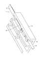
- FIG. 1 Perspective view of a connection structure of a flat electric wire according to an embodiment
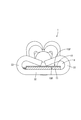
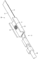
- FIG. 1 Front view of connection structure of flat electric wire of embodiment
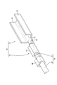
- FIG. 1 a perspective view of a terminal fitting to which an electric wire is connected.
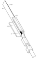
- Perspective view of a flat electric wire according to an embodiment a perspective view showing a state where a flat electric wire is mounted on a mounting plate portion.
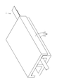
- a perspective view showing a state where a connection portion between a flat electric wire, an electric wire, and a terminal fitting is accommodated in a protective case.
- a perspective view showing a state where a connection portion between a flat electric wire, an electric wire, and a terminal fitting is accommodated in a lower case.
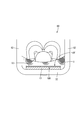
- Perspective view of connection structure of flat electric wire of modified example Front view of connection structure of flat electric wire of modified example
- a connection structure 1 for a flat electric wire 10 includes a flat electric wire 10, an electric wire 20, and a terminal fitting 30 for connecting the both.
- the flat electric wire 10 is formed of a flexible printed circuit board (FPC), and has a flat shape having a front surface 10F (corresponding to another surface) and a back surface 10R (corresponding to one surface), as shown in FIG.
- the flat electric wire 10 includes a strip-shaped conductor path 11 formed of a copper foil, and an insulating resin film 12 (insulating layer) covering both surfaces of the conductor path 11.
- the insulating resin film 12 on the surface 10F is deleted, and the conductor path 11 is exposed.
- a reinforcing plate 13 for reinforcing the distal end is provided on the rear surface 10R of the flat electric wire 10 so as to cover the entire rear surface 10R of the distal end.
- the reinforcing plate 13 is made of, for example, a glass epoxy resin or a polyimide resin. 1, 2, and 7, the conductor path 11 and the insulating resin film 12 are not shown, but the entire flat electric wire 10 is schematically shown.
- the electric wire 20 includes a core wire 21 composed of a stranded wire obtained by twisting a plurality of copper or copper alloy strands, and a synthetic resin insulating coating 22 that covers the core wire 21. And a copper wire having a known configuration. At the terminal portion of the electric wire 20, the insulating coating 22 is peeled off, and the core wire 21 is exposed.
- the terminal fitting 30 includes a first connection portion 31 (corresponding to a connection portion) to which the flat electric wire 10 is connected, and a second connection portion 41 to which the electric wire 20 is connected.
- the first connection portion 31 has a U-shape as shown in FIG.
- the portion corresponding to the bottom of the U-shape is a flat mounting plate portion 32 (corresponding to a mounting portion) on which the distal end portion of the flat electric wire 10 is mounted.
- a portion corresponding to the two vertical sides of the U-shape extending vertically from the mounting plate portion 32 is a dam wall 33 (corresponding to a dam portion).
- the front end portion of the flat electric wire 10 overlaps with the mounting plate portion 32 so as to be sandwiched between the two dam walls 33.
- the front end of the flat electric wire 10 is configured such that the back surface 10R on which the reinforcing plate 13 is disposed faces the mounting plate portion 32, and the surface 10F where the conductor paths 11 are exposed faces the opposite side to the mounting plate portion 32. And is placed on the mounting plate portion 32.
- the surface 10F where the conductor path 11 is exposed is covered with solder H, and the conductor path 11 and the first connection portion 31 are electrically connected by the solder H.
- the two dam walls 33 are bent inward so that the tips (edges opposite to the mounting plate 32) abut each other, and cover the tip of the flat electric wire 10 and the solder H attached to the surface 10F. ing.
- the second connection portion 41 includes a band-shaped bottom plate 42 continuous from the mounting plate portion 32, a pair of wire barrels 43 rising from the bottom plate 42, and a pair of insulation barrels 44 rising from the bottom plate 42.
- the wire barrel 43 is crimped to the core wire 21 exposed from the insulating coating 22 at the end of the electric wire 20, and the insulation barrel 44 is crimped to a portion of the electric wire 20 covered with the insulating coating 22, so that the electric wire 20 is It is connected to the second connection part 41.
- the tip of the flat wire 10 is placed on the placement plate 32.
- the back surface 10R on which the reinforcing plate 13 is disposed faces the mounting plate portion 32
- the front surface 10F where the conductor paths 11 are exposed faces the opposite side to the mounting plate portion 32.
- solder H is applied to the surface 10F where the conductor path 11 is exposed, and the conductor path 11 and the first connection part 31 are connected by soldering.
- the solder H accumulates inside the U-shape surrounded by the mounting plate portion 32 and the two dam walls 33, and the solder H is prevented from flowing out, so that the solder fillet is formed satisfactorily.
- the two dam walls 33 are bent inward so that their tips abut each other.
- the connection portion between the flat electric wire 10, the electric wire 20, and the terminal fitting 30 is accommodated in the protective case 50 and protected as shown in FIGS.
- the protection case 50 includes a lower case 51 having an accommodation groove 52 for accommodating a connection portion between the flat electric wire 10, the electric wire 20, and the terminal fitting 30. And an upper case 53 that covers the portion.
- connection structure 1 of the flat electric wire 10 is connected to the flat electric wire 10 including the strip-shaped conductor path 11 and the insulating resin film 12 covering the conductor path 11, and is connected to the flat electric wire 10.
- a solder H for electrically connecting the conductor path 11 and the first connection portion 31.
- the first connection portion 31 includes a mounting plate portion 32 on which the flat electric wire 10 is mounted, and a pair of dam walls 33 connected to the mounting plate portion 32 and arranged with the flat electric wire 10 interposed therebetween.
- the flat electric wire 10 has a back surface 10R facing the mounting plate portion 32 and a front surface 10F opposite to the back surface 10R, and the conductor path 11 is exposed from the insulating resin film 12 on the front surface 10F.
- the solder H is overlaid.
- the solder H when the conductor path 11 and the first connection portion 31 are connected by the solder H, the solder H is dammed by the damming wall 33, and is prevented from flowing out of the mounting plate portion 32. Therefore, the solder fillet is formed favorably, and the connection reliability between the flat electric wire 10 and the terminal fitting 30 can be secured.
- the dam wall 33 is arranged so as to face the surface 10F of the flat electric wire 10. According to such a configuration, the strength of the connection portion between the flat electric wire 10 and the terminal fitting 30 is improved.
- FIGS. 8 and 9 show a connection structure 60 of a flat electric wire 10 according to a modification.
- the terminal fitting 61 of the present modified example after the soldering, the two dam walls 62 are not bent and remain standing from the mounting plate portion 32. Even in such a configuration, similar to the embodiment, at the time of soldering, the solder H is dammed by the damping wall 62 and is prevented from flowing out of the mounting plate portion 32. It is formed well, and the connection reliability between the flat electric wire 10 and the terminal fitting 61 can be secured.
- the configuration other than the above is the same as that of the embodiment.
- the flat electric wire 10 is configured by the FPC, but is not limited thereto, and may be configured by, for example, a flexible flat cable (FFC).
- FFC flexible flat cable
- the terminal fitting 30 includes the second connection portion 41 connected to the electric wire 20.
- the terminal fitting includes a terminal connection portion connected to another terminal fitting. It does not matter.
Landscapes
- Coupling Device And Connection With Printed Circuit (AREA)
- Multi-Conductor Connections (AREA)
- Connections Effected By Soldering, Adhesion, Or Permanent Deformation (AREA)
Abstract
フラット電線の接続構造1は、帯状の導体路11と、導体路11を被覆する絶縁樹脂フィルム12とを備えるフラット電線10と、フラット電線10と接続される第1接続部31を備える端子金具30と、導体路11と第1接続部31とを電気的に接続する半田とを備える。第1接続部31が、フラット電線10が載置される載置板部32と、載置板部32から連なり、フラット電線10を挟んで配置される一対のせき止め壁33とを備えており、フラット電線10が、載置板部32に対向する裏面10Rと、裏面10Rと反対側の表面10Fとを有し、表面10Fにおいて導体路11が絶縁樹脂フィルム12から露出されており、表面10Fに半田Hが重ねられている。
Description
本明細書によって開示される技術は、フラット電線の接続構造に関する。
フラットケーブルの導体路に電線の芯線を重ね、はんだ付けにより導体路と芯線とを接続した構造が知られている(特許文献1参照)。
上記のような接続構造では、電線に強い力が加えられた場合に、接合部に亀裂が入るなどして、接続信頼性が低下するおそれがあった。
本明細書によって開示されるフラット電線の接続構造は、帯状の導体路と、前記導体路を被覆する絶縁層とを備えるフラット電線と、前記フラット電線と接続される接続部を備える端子金具と、前記導体路と前記接続部とを電気的に接続する半田とを備え、前記接続部が、前記フラット電線が載置される載置部と、前記載置部から連なり、前記フラット電線を挟んで配置される一対のせき止め部とを備えており、前記フラット電線が、前記載置部に対向する一面と、前記一面と反対側の他面とを有し、前記他面において前記導体路が前記絶縁層から露出されており、前記他面に前記半田が重ねられている。
上記の構成によれば、導体路と接続部とを半田によって接続する際に、半田がせき止め部によってせき止められ、載置部の外側に流れ出すことが規制されるので、半田フィレットが良好に形成され、フラット電線と端子金具との接続信頼性を確保できる。
上記の構成において、前記せき止め部が、前記フラット電線の他面に対向して配置されていても構わない。このような構成によれば、せき止め部が、フラット電線の他面に対向して配置されているので、フラット電線と端子金具との接続部分の強度が向上する。
本明細書によって開示されるフラット電線の接続構造によれば、フラット電線と端子金具との接続信頼性を確保できる。
<実施形態>
実施形態を、図1~図7を参照しつつ説明する。本実施形態のフラット電線10の接続構造1は、図1に示すように、フラット電線10と、電線20と、両者を接続する端子金具30とを備えている。
実施形態を、図1~図7を参照しつつ説明する。本実施形態のフラット電線10の接続構造1は、図1に示すように、フラット電線10と、電線20と、両者を接続する端子金具30とを備えている。
フラット電線10は、フレキシブルプリント基板(FPC)によって構成され、図4に示すように、表面10F(他面に該当)と、裏面10R(一面に該当)とを有する平板状をなしている。このフラット電線10は、銅箔によって形成された帯状の導体路11と、導体路11の両面を被覆する絶縁樹脂フィルム12(絶縁層)とを備えている。フラット電線10の先端部においては、表面10Fの絶縁樹脂フィルム12が削除されて導体路11が露出されている。一方、フラット電線10の裏面10Rには、先端部を補強する補強板13が、先端部の裏面10R全体を覆うように設けられている。補強板13は、例えば、ガラスエポシキ樹脂、あるいはポリイミド樹脂等によって構成される。なお、図1、図2および図7では、導体路11と絶縁樹脂フィルム12とを示さず、フラット電線10全体を模式的に示している。
電線20は、図3に示すように、銅または銅合金製の素線の複数本を撚り合わせた撚り線によって構成された芯線21と、この芯線21を被覆する合成樹脂製の絶縁被覆22とを備えた、周知の構成の銅電線である。電線20の端末部においては、絶縁被覆22が剥き取られて芯線21が露出されている。
端子金具30は、図3に示すように、フラット電線10が接続される第1接続部31(接続部に該当)と、電線20が接続される第2接続部41とを備えている。
第1接続部31は、フラット電線10に接続される前の状態では、図3に示すように、U字状をなしている。U字の底部に相当する部分は、フラット電線10の先端部が載置される平板状の載置板部32(載置部に該当)となっている。この載置板部32から垂直に延びる、U字の2つの縦辺に相当する部分は、せき止め壁33(せき止め部に該当)となっている。
第1接続部31がフラット電線10に接続された状態では、図2に示すように、フラット電線10の先端部が、2つのせき止め壁33に挟まれるようにして、載置板部32に重ねられている。フラット電線10の先端部は、補強板13が配された裏面10Rが載置板部32と対向し、導体路11が露出された表面10Fが載置板部32とは反対側を向くようにして、載置板部32に重ねられている。フラット電線10の先端部において、導体路11が露出された表面10Fは、半田Hによって覆われており、この半田Hによって導体路11と第1接続部31とが電気的に接続されている。2つのせき止め壁33は、互いに先端(載置板部32と反対側の端縁)が突き合わせられるように内側に折れ曲がり、フラット電線10の先端部と、その表面10Fに付着した半田Hとを覆っている。
第2接続部41は、図3に示すように、載置板部32から連なる帯状の底板42と、この底板42から立ち上がる一対のワイヤーバレル43と、同じく底板42から立ち上がる一対のインシュレーションバレル44とを備えている。ワイヤーバレル43が、電線20の端末において絶縁被覆22から露出された芯線21に圧着され、インシュレーションバレル44が、電線20において絶縁被覆22に覆われた部分に圧着されることで、電線20が第2接続部41に接続されている。
フラット電線10と第1接続部31とを接続する際には、まず、図5に示すように、フラット電線10の先端部を、載置板部32上に載置する。このとき、補強板13が配された裏面10Rが載置板部32と対向し、導体路11が露出された表面10Fが載置板部32とは反対側を向くようにする。次に、先端部において、導体路11が露出された表面10Fに、半田Hを塗布し、半田付けにより導体路11と第1接続部31とを接続する。このとき、載置板部32と2つのせき止め壁33とで囲まれたU字の内側に半田Hが溜まり、半田Hが外に流れ出ないようになっているので、半田フィレットが良好に形成される。その後、2つのせき止め壁33を、先端が互いに突き合わせられるように内側に折り曲げる。このようにして、フラット電線10と第1接続部31との接続が完了する。
フラット電線10と、電線20と、端子金具30との接続部分は、図6および図7に示すように、保護ケース50に収容され、保護される。保護ケース50は、フラット電線10と、電線20と、端子金具30との接続部分を収容する収容溝52を有する下ケース51と、この下ケース51に組み付けられて収容溝52に収容された接続部分を覆う上ケース53とを備えている。
以上のように本実施形態によれば、フラット電線10の接続構造1は、帯状の導体路11と、導体路11を被覆する絶縁樹脂フィルム12とを備えるフラット電線10と、フラット電線10と接続される第1接続部31を備える端子金具30と、導体路11と第1接続部31とを電気的に接続する半田Hとを備える。第1接続部31が、フラット電線10が載置される載置板部32と、載置板部32から連なり、フラット電線10を挟んで配置される一対のせき止め壁33とを備えており、フラット電線10が、載置板部32に対向する裏面10Rと、裏面10Rと反対側の表面10Fとを有し、表面10Fにおいて導体路11が絶縁樹脂フィルム12から露出されており、表面10Fに半田Hが重ねられている。
上記の構成によれば、導体路11と第1接続部31とを半田Hによって接続する際に、半田Hがせき止め壁33によってせき止められ、載置板部32の外側に流れ出すことが規制されるので、半田フィレットが良好に形成され、フラット電線10と端子金具30との接続信頼性を確保できる。
また、せき止め壁33が、フラット電線10の表面10Fに対向して配置されている。このような構成によれば、フラット電線10と端子金具30との接続部分の強度が向上する。
<変形例>
変形例のフラット電線10の接続構造60を図8および図9に示す。本変形例の端子金具61においては、半田付け後に、2つのせき止め壁62が折り曲げ加工されず、載置板部32から立ち上がったままとされている。このような構成であっても、実施形態と同様に、半田付けの際に、半田Hがせき止め壁62によってせき止められ、載置板部32の外側に流れ出すことが規制されるので、半田フィレットが良好に形成され、フラット電線10と端子金具61との接続信頼性を確保できる。なお、本変形例において、上記以外の構成は実施形態と同様であるので、同一の構成には同一の符号を付して説明を省略する。
変形例のフラット電線10の接続構造60を図8および図9に示す。本変形例の端子金具61においては、半田付け後に、2つのせき止め壁62が折り曲げ加工されず、載置板部32から立ち上がったままとされている。このような構成であっても、実施形態と同様に、半田付けの際に、半田Hがせき止め壁62によってせき止められ、載置板部32の外側に流れ出すことが規制されるので、半田フィレットが良好に形成され、フラット電線10と端子金具61との接続信頼性を確保できる。なお、本変形例において、上記以外の構成は実施形態と同様であるので、同一の構成には同一の符号を付して説明を省略する。
<他の実施形態>
本明細書によって開示される技術は上記記述及び図面によって説明した実施形態に限定されるものではなく、例えば次のような種々の態様も含まれる。
(1)上記実施形態および変形例では、フラット電線10は、FPCにより構成されていたが、これに限らず、例えばフレキシブルフラットケーブル(FFC)により構成されていても構わない。
本明細書によって開示される技術は上記記述及び図面によって説明した実施形態に限定されるものではなく、例えば次のような種々の態様も含まれる。
(1)上記実施形態および変形例では、フラット電線10は、FPCにより構成されていたが、これに限らず、例えばフレキシブルフラットケーブル(FFC)により構成されていても構わない。
(2)上記実施形態では、端子金具30が、電線20に接続される第2接続部41を備えていたが、例えば、端子金具が、他の端子金具と接続される端子接続部を備えていても構わない。
1、60…フラット電線の接続構造
10…フラット電線
10F…表面(他面)
10R…裏面(一面)
11…導体路
12…絶縁樹脂フィルム(絶縁層)
30…端子金具
31…第1接続部(接続部)
32…載置板部(載置部)
33、62…せき止め壁(せき止め部)
H…半田
10…フラット電線
10F…表面(他面)
10R…裏面(一面)
11…導体路
12…絶縁樹脂フィルム(絶縁層)
30…端子金具
31…第1接続部(接続部)
32…載置板部(載置部)
33、62…せき止め壁(せき止め部)
H…半田
Claims (2)
- 帯状の導体路と、前記導体路を被覆する絶縁層とを備えるフラット電線と、
前記フラット電線と接続される接続部を備える端子金具と、
前記導体路と前記接続部とを電気的に接続する半田とを備え、
前記接続部が、前記フラット電線が載置される載置部と、前記載置部から連なり、前記フラット電線を挟んで配置される一対のせき止め部とを備えており、
前記フラット電線が、前記載置部に対向する一面と、前記一面と反対側の他面とを有し、前記他面において前記導体路が前記絶縁層から露出されており、
前記他面に前記半田が重ねられている、フラット電線の接続構造。 - 前記せき止め部が、前記フラット電線の他面に対向して配置されている、請求項1に記載のフラット電線の接続構造。
Priority Applications (2)
| Application Number | Priority Date | Filing Date | Title |
|---|---|---|---|
| CN201980046824.3A CN112514169B (zh) | 2018-07-26 | 2019-07-05 | 扁平电线的连接构造 |
| US17/262,373 US20210305723A1 (en) | 2018-07-26 | 2019-07-05 | Joint structure for connection of flat electric wire assembly |
Applications Claiming Priority (2)
| Application Number | Priority Date | Filing Date | Title |
|---|---|---|---|
| JP2018-140354 | 2018-07-26 | ||
| JP2018140354A JP7001561B2 (ja) | 2018-07-26 | 2018-07-26 | フラット電線の接続構造 |
Publications (1)
| Publication Number | Publication Date |
|---|---|
| WO2020022033A1 true WO2020022033A1 (ja) | 2020-01-30 |
Family
ID=69181681
Family Applications (1)
| Application Number | Title | Priority Date | Filing Date |
|---|---|---|---|
| PCT/JP2019/026792 Ceased WO2020022033A1 (ja) | 2018-07-26 | 2019-07-05 | フラット電線の接続構造 |
Country Status (4)
| Country | Link |
|---|---|
| US (1) | US20210305723A1 (ja) |
| JP (1) | JP7001561B2 (ja) |
| CN (1) | CN112514169B (ja) |
| WO (1) | WO2020022033A1 (ja) |
Families Citing this family (1)
| Publication number | Priority date | Publication date | Assignee | Title |
|---|---|---|---|---|
| CN115939814A (zh) * | 2022-12-27 | 2023-04-07 | 鹤山市柏拉蒂电子有限公司 | 线芯连接结构 |
Citations (3)
| Publication number | Priority date | Publication date | Assignee | Title |
|---|---|---|---|---|
| JPS60178976U (ja) * | 1984-05-10 | 1985-11-28 | 古河電気工業株式会社 | フラツトケ−ブルとリ−ド線の接続部 |
| JPS63112787U (ja) * | 1987-01-16 | 1988-07-20 | ||
| JPH0279130A (ja) * | 1988-09-16 | 1990-03-19 | Mitsubishi Electric Corp | 信号線駆動方式 |
Family Cites Families (16)
| Publication number | Priority date | Publication date | Assignee | Title |
|---|---|---|---|---|
| JPS6414883A (en) * | 1987-07-09 | 1989-01-19 | Masaichi Sato | Connection terminal for electric wire and connection of electric wire to its terminal |
| JPH0640427Y2 (ja) * | 1988-12-01 | 1994-10-19 | アルプス電気株式会社 | フラツトケーブルとリード線の接続構造 |
| JP3132985B2 (ja) * | 1995-06-12 | 2001-02-05 | ソニー株式会社 | コンタクトにおける接続端子部構造 |
| JP2002260761A (ja) * | 2001-02-28 | 2002-09-13 | Yazaki Corp | 中継コネクタ |
| DE10139797A1 (de) * | 2001-08-14 | 2003-02-27 | Bsh Bosch Siemens Hausgeraete | Elektrische Steckverbindung |
| JP2003217709A (ja) * | 2002-01-17 | 2003-07-31 | Yazaki Corp | フラットケーブルの接続構造 |
| JP2006172927A (ja) * | 2004-12-16 | 2006-06-29 | Yazaki Corp | 電線の超音波接合方法及び超音波接合装置 |
| JP5242112B2 (ja) * | 2007-10-02 | 2013-07-24 | 古河電気工業株式会社 | フレキシブルフラットハーネス及びその製造方法並びにスライドドアの給電装置 |
| JP4825906B2 (ja) * | 2009-08-28 | 2011-11-30 | 株式会社オートネットワーク技術研究所 | アルミ電線と銅端子の接続構造およびこの接続構造を有する銅端子付きアルミ電線 |
| JP5884986B2 (ja) * | 2012-07-31 | 2016-03-15 | 矢崎総業株式会社 | 圧着端子付きアルミ電線 |
| JP6028934B2 (ja) * | 2013-12-19 | 2016-11-24 | 住友電装株式会社 | 端子付電線 |
| JP2016091899A (ja) * | 2014-11-07 | 2016-05-23 | 第一精工株式会社 | ケーブルクランプ及びケーブルクランプ接続構造体 |
| DE102014117829B3 (de) * | 2014-12-04 | 2016-01-14 | "Konfektion E" Elektronik Gmbh | Elektrisches Kontaktteil und Verfahren zum Verbinden des Kontaktteils |
| JP6545530B2 (ja) * | 2015-05-28 | 2019-07-17 | 田淵電機株式会社 | 電線端部の端子接続構造およびその製造方法 |
| JP2017152224A (ja) * | 2016-02-25 | 2017-08-31 | 住友電装株式会社 | 芯線と接合対象物との接合物、端子、超音波接合装置、及び、芯線と接合対象物との接合方法 |
| CN107342466B (zh) * | 2017-06-05 | 2019-07-16 | 吉林省中赢高科技有限公司 | 一种铜端子与铝导线的接头及其超声波焊接方法 |
-
2018
- 2018-07-26 JP JP2018140354A patent/JP7001561B2/ja active Active
-
2019
- 2019-07-05 CN CN201980046824.3A patent/CN112514169B/zh active Active
- 2019-07-05 US US17/262,373 patent/US20210305723A1/en not_active Abandoned
- 2019-07-05 WO PCT/JP2019/026792 patent/WO2020022033A1/ja not_active Ceased
Patent Citations (3)
| Publication number | Priority date | Publication date | Assignee | Title |
|---|---|---|---|---|
| JPS60178976U (ja) * | 1984-05-10 | 1985-11-28 | 古河電気工業株式会社 | フラツトケ−ブルとリ−ド線の接続部 |
| JPS63112787U (ja) * | 1987-01-16 | 1988-07-20 | ||
| JPH0279130A (ja) * | 1988-09-16 | 1990-03-19 | Mitsubishi Electric Corp | 信号線駆動方式 |
Also Published As
| Publication number | Publication date |
|---|---|
| CN112514169B (zh) | 2022-08-19 |
| CN112514169A (zh) | 2021-03-16 |
| JP7001561B2 (ja) | 2022-01-19 |
| JP2020017431A (ja) | 2020-01-30 |
| US20210305723A1 (en) | 2021-09-30 |
Similar Documents
| Publication | Publication Date | Title |
|---|---|---|
| JP7136288B2 (ja) | シールドフラットケーブル | |
| JP5365389B2 (ja) | 同軸ケーブルハーネス | |
| US9882306B2 (en) | Cable connector and carrier module thereof | |
| JP4816724B2 (ja) | シールドフラットケーブル | |
| CN102948252A (zh) | 用于存在于平面结构、尤其是玻璃板上的导体的接触装置 | |
| JP4897964B2 (ja) | 電流検出装置 | |
| JP6855109B2 (ja) | 導体接続構造体 | |
| US12144107B2 (en) | Substrate connection structure and vehicle wiring module | |
| JP2021197261A5 (ja) | ||
| JP6531292B2 (ja) | プリント配線基板 | |
| JP2020017431A (ja) | フラット電線の接続構造 | |
| JP5927435B2 (ja) | 電子装置 | |
| TWI469158B (zh) | 過電流保護元件 | |
| JP5114297B2 (ja) | グランドバー及びケーブルアセンブリ | |
| JP2013112122A (ja) | ウインドガラス構造 | |
| JP4470935B2 (ja) | 多心同軸ケーブルおよびその製造方法 | |
| JP2005050971A (ja) | フレキシブル回路基板 | |
| KR20140016802A (ko) | 전선 커넥터 | |
| KR20170108772A (ko) | 탄성 전기접촉단자 | |
| KR100612299B1 (ko) | 커넥터가 장착되는 가요성 인쇄회로 기판 | |
| KR102965225B1 (ko) | 연결케이스 장치 및 이를 가진 와이어링 하니스 | |
| JPH1075029A (ja) | フレキシブルプリント基板の連結構造 | |
| TWM444625U (zh) | 卡緣線纜連接器組合(三) | |
| JP3266459B2 (ja) | 極細同軸線使用のジャンパーアセンブリー | |
| CN111585138B (zh) | 电缆和制造电缆的方法 |
Legal Events
| Date | Code | Title | Description |
|---|---|---|---|
| 121 | Ep: the epo has been informed by wipo that ep was designated in this application |
Ref document number: 19841588 Country of ref document: EP Kind code of ref document: A1 |
|
| NENP | Non-entry into the national phase |
Ref country code: DE |
|
| 122 | Ep: pct application non-entry in european phase |
Ref document number: 19841588 Country of ref document: EP Kind code of ref document: A1 |