WO2020021652A1 - 半導体装置 - Google Patents
半導体装置 Download PDFInfo
- Publication number
- WO2020021652A1 WO2020021652A1 PCT/JP2018/027881 JP2018027881W WO2020021652A1 WO 2020021652 A1 WO2020021652 A1 WO 2020021652A1 JP 2018027881 W JP2018027881 W JP 2018027881W WO 2020021652 A1 WO2020021652 A1 WO 2020021652A1
- Authority
- WO
- WIPO (PCT)
- Prior art keywords
- region
- semiconductor
- buried
- conductivity type
- semiconductor device
- Prior art date
- Legal status (The legal status is an assumption and is not a legal conclusion. Google has not performed a legal analysis and makes no representation as to the accuracy of the status listed.)
- Ceased
Links
Images


Classifications
-
- H—ELECTRICITY
- H10—SEMICONDUCTOR DEVICES; ELECTRIC SOLID-STATE DEVICES NOT OTHERWISE PROVIDED FOR
- H10D—INORGANIC ELECTRIC SEMICONDUCTOR DEVICES
- H10D30/00—Field-effect transistors [FET]
- H10D30/60—Insulated-gate field-effect transistors [IGFET]
Definitions
- the present invention relates to a semiconductor device in which a current path of a main current is parallel to a main surface.
- a structure is disclosed in which a field plate is arranged between a gate electrode and a drain region of a MOSFET (metal oxide semiconductor field effect transistor) (see Patent Document 1).
- MOSFET metal oxide semiconductor field effect transistor
- the breakdown voltage of the semiconductor device is improved by arranging the field plate on the thermal oxide film formed between the gate electrode and the drain region.
- An object of the present invention is to provide a lateral semiconductor device capable of improving withstand voltage.
- a semiconductor substrate of a first conductivity type a buried region of a second conductivity type buried in a part of the upper surface of the semiconductor substrate, and a buried region selectively covering the buried region on the upper surface of the semiconductor substrate.
- a second conductive type first semiconductor region having a lower impurity concentration than the buried region, and a first conductive region disposed on the upper surface of the semiconductor substrate in a remaining region of the region where the first semiconductor region is disposed.
- a gate electrode disposed above the second semiconductor region between the drain region and the source region.
- the position of the opposite end of the buried region facing the second semiconductor region in plan view is the drain of the gate electrode.
- the edge near the region and the gate voltage of the drain region The semiconductor device is provided which is between the near side of the end portion.
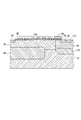
- FIG. 2 is a schematic cross-sectional view illustrating a structure of a semiconductor device according to an embodiment of the present invention.
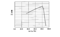
- 6 is a graph showing the relationship between the position of the opposite end of the buried region and the breakdown voltage of the semiconductor device.
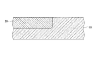
- FIG. 4 is a schematic cross-sectional view for explaining the method for manufacturing the semiconductor device according to the embodiment of the present invention (part 1).
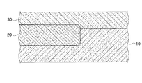
- FIG. 9 is a schematic cross-sectional view for explaining the method for manufacturing the semiconductor device according to the embodiment of the present invention (part 2).
- FIG. 7 is a schematic cross-sectional view for explaining the method for manufacturing the semiconductor device according to the embodiment of the present invention (part 3).
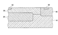
- FIG. 9 is a schematic cross-sectional view for explaining the method for manufacturing the semiconductor device according to the embodiment of the present invention (part 4).
- FIG. 9 is a schematic cross-sectional view illustrating a structure of a semiconductor device according to another embodiment of the present invention.
- the semiconductor device includes a buried region 20 of a second conductivity type buried in a part of the upper surface of a semiconductor substrate 10 of a first conductivity type, and covers the buried region 20. And a first semiconductor region 30 of the second conductivity type selectively disposed on the upper surface of the semiconductor substrate 10.
- the buried region 20 is in contact with the semiconductor substrate 10, and the first semiconductor region 30 is in contact with the semiconductor substrate 10 in a region where the buried region 20 is not arranged.
- the impurity concentration of the first semiconductor region 30 is set lower than the impurity concentration of the buried region 20.
- the semiconductor device shown in FIG. 1 further includes a second semiconductor region 40 of the first conductivity type disposed on the upper surface of the semiconductor substrate 10 in the remaining region where the first semiconductor region 30 is disposed.
- the second conductivity type drain region 50 is disposed on a part of the upper surface of the first semiconductor region 30, and the second conductivity type source region 60 is formed on a part of the upper surface of the second semiconductor region 40.
- a gate electrode 80 is disposed above the second semiconductor region 40 via a gate insulating film 70.
- the end of the buried region 20 facing the second semiconductor region 40 (hereinafter referred to as “opposite end”) in plan view is positioned closer to the drain region 50 of the gate electrode 80. Between the end and the end of the drain region 50 on the side closer to the gate electrode 80.
- the first conductivity type and the second conductivity type are opposite to each other. That is, if the first conductivity type is p-type, the second conductivity type is n-type, and if the first conductivity type is n-type, the second conductivity type is p-type.
- the first conductivity type is p-type and the second conductivity type is n-type will be described as an example.
- the semiconductor device shown in FIG. 1 is a lateral transistor in which a main current flows between the source region 60 and the drain region 50 in parallel with the main surface of the semiconductor substrate 10 in the ON operation.
- a basic operation of the semiconductor device illustrated in FIG. 1 will be described.
- the semiconductor device is turned on by controlling the potential of the gate electrode 80 in a state where a positive potential is applied to the drain region 50 with reference to the potential of the source region 60. That is, by setting the voltage between the gate electrode 80 and the source region 60 to a predetermined threshold voltage or more, a channel is formed in the second semiconductor region 40 below the gate electrode 80. Thereby, a main current flows between the source region 60 and the drain region 50.
- the voltage between the gate electrode 80 and the source region 60 is set lower than a predetermined threshold voltage. As a result, the channel disappears and the main current is cut off.
- the opposite end of the buried region 20 has an end on the side closer to the drain region 50 in a region where a channel is formed below the gate electrode 80 in the ON operation (hereinafter, referred to as a “channel forming region”), and It is located between the region 50.
- the depletion layer spreads from the pn junction at the interface between the semiconductor substrate 10 and the second semiconductor region 40 of the first conductivity type and the first semiconductor region 30 and the buried region 20 of the second conductivity type. Since the buried region 20 has a higher impurity concentration than the first semiconductor region 30, the depletion layer is formed at the interface between the buried region 20 and the semiconductor substrate 10 rather than at the interface between the first semiconductor region 30 and the semiconductor substrate 10. Stretch long to the side. Therefore, the breakdown voltage of the semiconductor device shown in FIG. 1 can be improved as compared with the semiconductor device having no buried region 20. By making the area where the semiconductor substrate 10 contacts the buried region 20 larger than the area where the semiconductor substrate 10 contacts the first semiconductor region 30, the breakdown voltage of the semiconductor device can be further improved.
- FIG. 2 shows the results of the investigation.
- the vertical axis in FIG. 2 is the breakdown voltage of the semiconductor device.
- the horizontal axis in FIG. 2 indicates the distance La from the end of the drain region 50 closer to the drain region 50 to the distance La to the end of the buried region 20 closer to the drain region 50 when the end is closer to the gate electrode 80. This is the value of the ratio of the distance Lb to the opposing end (hereinafter, referred to as “Lb / La ratio”).
- the distance La and the distance Lb are distances in plan view.
- the breakdown voltage of the semiconductor device shown in FIG. 1 is shown by a solid line, and the breakdown voltage of the semiconductor device having no buried region 20 is shown by a broken line for reference.
- the withstand voltage of the semiconductor device decreases as shown in FIG. This is because if the buried region 20 is extended too much toward the gate electrode 80, the lateral expansion of a depletion layer formed between the first semiconductor region 30 and the second semiconductor region 40 is suppressed. . That is, before the depletion layer spreads sufficiently, breakdown voltage breakdown occurs between the first semiconductor region 30 and the second semiconductor region 40, and the breakdown voltage of the semiconductor device decreases.
- the breakdown withstand voltage first occurs at the interface between the buried region 20 and the semiconductor substrate 10. Occurs.
- the position of the opposing end of the buried region 20 is moved closer to the second semiconductor region 40 beyond the maximum breakdown voltage position, breakdown breakdown occurs first at the interface between the first semiconductor region 30 and the second semiconductor region 40. .
- the breakdown voltage increases at the interface between the buried region 20 and the semiconductor substrate 10. Greatly decreases.
- the opposite end of the buried region 20 is connected to the end of the gate electrode 80 closer to the drain region 50 and closer to the gate electrode 80 of the drain region 50. Between the side ends. Thereby, the breakdown voltage of the semiconductor device can be improved. In particular, setting the Lb / La ratio to 80.5% improves the breakdown voltage of the semiconductor device.
- FIG. 1 a method for manufacturing the semiconductor device shown in FIG. 1 will be described with reference to the drawings.
- the method of manufacturing a semiconductor device described below is an example, and can be realized by various other manufacturing methods including this modification.
- a semiconductor substrate 10 of the first conductivity type is prepared.
- a p-type silicon substrate is used as the semiconductor substrate 10.
- the impurity concentration of the semiconductor substrate 10 is about 5.0 ⁇ 10 13 to 4.5 ⁇ 10 14 cm ⁇ 3 .
- a substrate other than a silicon substrate may be used as the semiconductor substrate 10.
- a buried region 20 is formed so as to be buried in a part of the upper surface of the semiconductor substrate 10.
- an n-type impurity is selectively ion-implanted into a part of the upper surface of the semiconductor substrate 10 using a mask material formed by a photolithography technique to form the buried region 20 at a predetermined position.
- the n-type impurity is, for example, arsenic or phosphorus.
- the thickness of the buried region 20 is about 15 to 25 ⁇ m, and the impurity concentration is about 1.1 ⁇ 10 15 to 1.5 ⁇ 10 15 cm ⁇ 3 .
- a first semiconductor region 30 is formed on the entire upper surface of the semiconductor substrate 10 so as to cover the buried region 20.
- the first semiconductor region 30 is formed by using an epitaxial growth method.
- the thickness of the first semiconductor region 30 is about 5 to 10 ⁇ m, and the impurity concentration is about 8.0 ⁇ 10 14 to 1.0 ⁇ 10 15 cm ⁇ 3 .
- a p-type impurity is selectively ion-implanted into a part of the first semiconductor region 30 to form a second semiconductor region 40.
- the second semiconductor region 40 is formed so as to reach the upper surface of the semiconductor substrate 10.
- the p-type impurity is, for example, boron.
- the thickness of the second semiconductor region 40 is about 10 to 15 ⁇ m, and the impurity concentration is about 5.0 ⁇ 10 15 to 1.0 ⁇ 10 18 cm ⁇ 3 .
- a drain region 50 and a source region 60 are formed.
- an n-type impurity is selectively implanted into a part of the upper portion of the first semiconductor region 30 by an ion implantation method using a mask material patterned using a photolithography technique as a mask to form the drain region 50.
- the source region 60 is formed by selectively implanting an n-type impurity into a part of the upper portion of the second semiconductor region 40.
- the gate insulating film 70 and the gate electrode 80 are formed at predetermined positions, and the semiconductor device shown in FIG. 1 is completed.
- the impurities in the buried region 20 diffuse around due to the influence of heat treatment in the manufacturing process after the buried region 20 is formed. Therefore, the upper part of the buried region 20 extends upward, and the interface between the buried region 20 and the first semiconductor region 30 is located higher than the interface between the semiconductor substrate 10 and the first semiconductor region 30.
- the breakdown voltage is reduced by disposing the buried region 20. It has been found that the effect of improving is remarkable.
- a field insulating film 90 is formed on the upper surface of the first semiconductor region 30 between the drain region 50 and the gate electrode 80, and the field plate 100 is disposed on the upper surface of the field insulating film 90. Is also good. By setting the field plate 100 to a predetermined potential, the electric field concentration at the end of the gate electrode 80 near the drain region 50 is reduced, and the withstand voltage of the semiconductor device can be further improved.
- a back gate region 110 of the first conductivity type is arranged on a part of the upper surface of the second semiconductor region 40.
- the first conductive type connection region 120 is buried in the upper portion of the semiconductor substrate 10 in contact with the lower surface of the second semiconductor region 40.
- the back gate region 110 and the semiconductor substrate 10 are electrically connected via the second semiconductor region 40 and the connection region 120.
- the semiconductor device is a MOSFET
- the semiconductor device may be a transistor having another structure.
- the present invention is applicable even when the semiconductor device is a JFET.
- the semiconductor device of the present invention can be used in the electronic equipment industry including the manufacturing industry for manufacturing horizontal semiconductor devices.
Landscapes
- Insulated Gate Type Field-Effect Transistor (AREA)
Abstract
第1導電型の半導体基板(10)の上面に埋め込まれた第2導電型の埋設領域(20)、埋設領域(20)を覆って半導体基板(10)の上面に配置され、埋設領域(20)よりも不純物濃度の低い第2導電型の第1半導体領域(30)、第1半導体領域(30)の配置された領域の残余の領域で、半導体基板(10)の上面に配置された第1導電型の第2半導体領域(40)、第1半導体領域(30)の上面に配置された第2導電型のドレイン領域(50)、第2半導体領域(40)の上面に配置された第2導電型のソース領域(60)、ドレイン領域(50)とソース領域(60)の間で第2半導体領域(40)の上方に配置されたゲート電極(80)を備え、埋設領域(20)の第2半導体領域(40)に対向する対向端の平面視の位置が、ゲート電極(80)のドレイン領域(50)に近い側の端部とドレイン領域(50)との間である。
Description
本発明は、主電流の電流経路が主面と平行である半導体装置に関する。
半導体装置の耐圧を向上させるために、種々の対策が検討されている。例えば、MOSFET(metal oxide semiconductor field effect transistor)のゲート電極とドレイン領域との間にフィールドプレートを配置する構造が開示されている(特許文献1参照。)。特許文献1に記載の発明では、ゲート電極とドレイン領域の間に形成された熱酸化膜の上にフィールドプレートを配置することによって、半導体装置の耐圧を向上させている。
近年、半導体装置の耐圧に対する要求は高まっている。これに対し、オン動作で流れる主電流が半導体基板の主面と平行である半導体装置(以下、「横型の半導体装置」という。)について十分な耐圧を実現することが困難になっている。本発明は、耐圧を向上できる横型の半導体装置を提供することを目的とする。
本発明の一態様によれば、第1導電型の半導体基板と、半導体基板の上面の一部に埋め込まれた第2導電型の埋設領域と、埋設領域を覆って半導体基板の上面に選択的に配置された、埋設領域よりも不純物濃度の低い第2導電型の第1半導体領域と、第1半導体領域の配置された領域の残余の領域で、半導体基板の上面に配置された第1導電型の第2半導体領域と、第1半導体領域の上面の一部に配置された第2導電型のドレイン領域と、第2半導体領域の上面の一部に配置された第2導電型のソース領域と、ドレイン領域とソース領域との間で第2半導体領域の上方に配置されたゲート電極とを備え、埋設領域の第2半導体領域に対向する対向端の平面視の位置が、ゲート電極のドレイン領域に近い側の端部と、ドレイン領域のゲート電極に近い側の端部との間である半導体装置が提供される。
本発明によれば、耐圧を向上できる横型の半導体装置を提供できる。
次に、図面を参照して、本発明の実施形態を説明する。以下の図面の記載において、同一又は類似の部分には同一又は類似の符号を付している。ただし、図面は模式的なものであり、各層の厚みの比率などは現実のものとは異なることに留意すべきである。したがって、具体的な厚みや寸法は以下の説明を参酌して判断すべきものである。また、図面相互間においても互いの寸法の関係や比率が異なる部分が含まれていることはもちろんである。
また、以下に示す実施形態は、この発明の技術的思想を具体化するための装置や方法を例示するものであって、この発明の実施形態は、構成部品の材質、形状、構造、配置などを下記のものに特定するものでない。この発明の実施形態は、請求の範囲において、種々の変更を加えることができる。
本発明の実施形態に係る半導体装置は、図1に示すように、第1導電型の半導体基板10の上面の一部に埋め込まれた第2導電型の埋設領域20と、埋設領域20を覆って半導体基板10の上面に選択的に配置された第2導電型の第1半導体領域30を備える。埋設領域20は半導体基板10と接しており、埋設領域20の配置されていない領域で、第1半導体領域30が半導体基板10と接している。第1半導体領域30の不純物濃度は、埋設領域20の不純物濃度よりも低く設定されている。
図1に示した半導体装置は、第1半導体領域30の配置された領域の残余の領域で、半導体基板10の上面に配置された第1導電型の第2半導体領域40を更に備える。図1に示すように、第2導電型のドレイン領域50が第1半導体領域30の上面の一部に配置され、第2導電型のソース領域60が第2半導体領域40の上面の一部に配置されている。更に、ドレイン領域50とソース領域60との間で、ゲート絶縁膜70を介してゲート電極80が第2半導体領域40の上方に配置されている。
図1に示す半導体装置において、埋設領域20の第2半導体領域40に対向する端部(以下において「対向端」という。)の平面視の位置は、ゲート電極80のドレイン領域50に近い側の端部と、ドレイン領域50のゲート電極80に近い側の端部との間である。
なお、第1導電型と第2導電型とは互いに反対導電型である。すなわち、第1導電型がp型であれば、第2導電型はn型であり、第1導電型がn型であれば、第2導電型はp型である。以下では、第1導電型がp型であり、第2導電型がn型である場合について例示的に説明する。
図1に示した半導体装置は、オン動作においてソース領域60とドレイン領域50の間に半導体基板10の主面と平行に主電流の流れる横型トランジスタである。以下に、図1に示した半導体装置の基本的な動作について説明する。
ソース領域60の電位を基準として、ドレイン領域50に正の電位を印加した状態でゲート電極80の電位を制御することにより、半導体装置がオン動作する。即ち、ゲート電極80とソース領域60間の電圧を所定の閾値電圧以上にすることにより、ゲート電極80の下方で第2半導体領域40にチャネルが形成される。これにより、ソース領域60とドレイン領域50間に主電流が流れる。
一方、オフ動作では、ゲート電極80とソース領域60間の電圧を所定の閾値電圧よりも低くする。これにより、チャネルが消滅し、主電流が遮断される。
したがって、埋設領域20の対向端は、オン動作においてチャネルがゲート電極80の下方で形成される領域(以下において、「チャネル形成領域」という。)のドレイン領域50に近い側の端部と、ドレイン領域50との間に位置する。
オフ動作では、第1導電型である半導体基板10及び第2半導体領域40と、第2導電型である第1半導体領域30及び埋設領域20との界面のpn接合から空乏層が広がる。第1半導体領域30よりも埋設領域20の不純物濃度の高いため、第1半導体領域30と半導体基板10との界面よりも、埋設領域20と半導体基板10との界面において、空乏層が半導体基板10側に長く延伸する。したがって、埋設領域20を有さない半導体装置と比べて、図1に示した半導体装置では耐圧を向上させることができる。半導体基板10と埋設領域20の接触する面積を、半導体基板10と第1半導体領域30の接触する面積よりも広くすることにより、半導体装置の耐圧をより向上できる。
更に、本発明者らは、埋設領域20の対向端の位置と半導体装置の逆バイアス時の耐圧との関係を調査した。調査結果を図2に示す。図2の縦軸は半導体装置の耐圧である。図2の横軸は、ドレイン領域50のゲート電極80に近い側の端部を基点とした場合の、ゲート電極80のドレイン領域50に近い側の端部までの距離Laに対する、埋設領域20の対向端までの距離Lbの比(以下、「Lb/La比」という。)の値である。距離La及び距離Lbは、平面視の距離である。なお、図1に示した半導体装置の耐圧を実線で示しており、参考として埋設領域20を有さない半導体装置の耐圧を破線で示した。
図2において最大の耐圧を示すのは、Lb/La比が80.5%の場合である。半導体装置の耐圧が最大となる埋設領域20の対向端の位置を、以下において「最大耐圧位置」という。また、図2に示すように、Lb/La比が0%より大きく、80.5%以下である場合には、埋設領域20を配置することにより耐圧が向上する。
埋設領域20の対向端が第2半導体領域40に近いほど、第1半導体領域30と半導体基板10との界面の距離に対して、埋設領域20と半導体基板10との界面の距離の比が長い。このため、半導体装置の耐圧が向上する。
しかし、埋設領域20の対向端が最大耐圧位置を越えて第2半導体領域40に近づいた場合には、図2に示すように半導体装置の耐圧が低下する。これは、埋設領域20をゲート電極80の側に延伸させすぎると、第1半導体領域30と第2半導体領域40の間に形成される空乏層の横方向の広がりが抑制されてしまうためである。つまり、空乏層が十分に広がる前に、第1半導体領域30と第2半導体領域40の間で耐圧破壊が生じ、半導体装置の耐圧が低下する。
本発明者らの調査によれば、埋設領域20の対向端の位置が最大耐圧位置とドレイン領域50との間にある場合には、埋設領域20と半導体基板10との界面で最初に耐圧破壊が生じる。一方、最大耐圧位置を越えて埋設領域20の対向端の位置を第2半導体領域40に近づけた場合には、第1半導体領域30と第2半導体領域40との界面で最初に耐圧破壊が生じる。図2に示すように、第1半導体領域30と第2半導体領域40との界面で耐圧破壊が生じる場合には、埋設領域20と半導体基板10との界面で耐圧破壊が生じる場合よりも、耐圧が大きく低下する。
以上に説明したように、本発明の実施形態に係る半導体装置では、埋設領域20の対向端を、ゲート電極80のドレイン領域50に近い側の端部と、ドレイン領域50のゲート電極80に近い側の端部との間に配置する。これにより、半導体装置の耐圧を向上させることができる。特に、Lb/La比を80.5%とすることにより、半導体装置の耐圧が向上する。
以下に、図面を参照して図1に示した半導体装置の製造方法を説明する。なお、以下に述べる半導体装置の製造方法は一例であり、この変形例を含めて、これ以外の種々の製造方法により実現可能である。
まず、第1導電型の半導体基板10を用意する。例えば、半導体基板10にp型のシリコン基板を用いる。半導体基板10の不純物濃度は、5.0×10¹³~4.5×1014cm-3程度である。なお、半導体基板10にシリコン基板以外の基板を使用してもよい。
そして、図3に示すように、半導体基板10の上面の一部に埋め込むようにして埋設領域20を形成する。例えば、フォトリソグラフィ技術により形成したマスク材を用いて、n型不純物を半導体基板10の上面の一部に選択的にイオン注入し、埋設領域20を所定の位置に形成する。n型不純物は、例えば砒素やリンなどである。埋設領域20の膜厚は15~25μm程度であり、不純物濃度は、1.1×10¹⁵~1.5×1015cm-3程度である。
次いで、図4に示すように、埋設領域20を覆うように、半導体基板10の上面の全面に第1半導体領域30を形成する。例えば、エピタキシャル成長法を用いて、第1半導体領域30を形成する。第1半導体領域30の膜厚は5~10μm程度であり、不純物濃度は8.0×10¹⁴~1.0×1015cm-3程度である。
次に、図5に示すように、第1半導体領域30の一部に選択的にp型不純物をイオン注入して、第2半導体領域40を形成する。このとき、半導体基板10の上面に達するように第2半導体領域40が形成される。p型不純物は、例えばボロンなどである。第2半導体領域40の膜厚は10~15μm程度であり、不純物濃度は、5.0×10¹⁵~1.0×1018cm-3程度である。
その後、図6に示すように、ドレイン領域50及びソース領域60を形成する。例えばフォトリソグラフィ技術を用いてパターニングしたマスク材をマスクにしたイオン注入法により、n型不純物を第1半導体領域30の上部の一部に選択的に注入してドレイン領域50を形成する。同様に、n型不純物を第2半導体領域40の上部の一部に選択的に注入してソース領域60を形成する。更に、ゲート絶縁膜70及びゲート電極80を所定の位置に形成して、図1に示す半導体装置が完成する。
なお、埋設領域20を形成した後の製造工程での熱処理の影響などにより、埋設領域20の不純物が周囲に拡散する。このため、埋設領域20の上部が上方に延伸し、半導体基板10と第1半導体領域30の界面よりも埋設領域20と第1半導体領域30の界面が上方に位置している。
本発明者らが検討を重ねた結果、半導体基板10、第1半導体領域30及び第2半導体領域40の不純物濃度の比率が一定の範囲にある場合に、埋設領域20を配置することによって耐圧を向上させる効果が顕著であることを見出した。
(その他の実施形態)
上記のように、本発明は実施形態によって記載したが、この開示の一部をなす論述及び図面はこの発明を限定するものであると理解すべきではない。この開示から当業者には様々な代替実施形態、実施例及び運用技術が明らかとなろう。
上記のように、本発明は実施形態によって記載したが、この開示の一部をなす論述及び図面はこの発明を限定するものであると理解すべきではない。この開示から当業者には様々な代替実施形態、実施例及び運用技術が明らかとなろう。
例えば、図7に示すように、ドレイン領域50とゲート電極80との間で第1半導体領域30の上面にフィールド絶縁膜90を形成し、フィールド絶縁膜90の上面にフィールドプレート100を配置してもよい。フィールドプレート100を所定の電位に設定することにより、ゲート電極80のドレイン領域50に近い側の端部における電界集中が緩和され、半導体装置の耐圧を更に向上させることができる。
なお、図7に示した半導体装置では、第2半導体領域40の上面の一部に、第1導電型のバックゲート領域110が配置されている。そして、第2半導体領域40の下面に接して、第1導電型の接続領域120が半導体基板10の上部に埋め込まれている。これにより、第2半導体領域40と接続領域120を介して、バックゲート領域110と半導体基板10が電気的に接続されている。
上記では半導体装置がMOSFETである場合を説明した。しかし、半導体装置が他の構造のトランジスタであってもよい。例えば、半導体装置がJFETの場合にも、本発明は適用可能である。
このように、本発明はここでは記載していない様々な実施形態等を含むことはもちろんである。
本発明の半導体装置は、横型の半導体装置を製造する製造業を含む電子機器産業に利用可能である。
10…半導体基板
20…埋設領域
30…第1半導体領域
40…第2半導体領域
50…ドレイン領域
60…ソース領域
70…ゲート絶縁膜
80…ゲート電極
20…埋設領域
30…第1半導体領域
40…第2半導体領域
50…ドレイン領域
60…ソース領域
70…ゲート絶縁膜
80…ゲート電極
Claims (3)
- 第1導電型の半導体基板と、
前記半導体基板の上面の一部に埋め込まれた第2導電型の埋設領域と、
前記埋設領域を覆って前記半導体基板の上面に選択的に配置された、前記埋設領域よりも不純物濃度の低い第2導電型の第1半導体領域と、
前記第1半導体領域の配置された領域の残余の領域で、前記半導体基板の上面に配置された第1導電型の第2半導体領域と、
前記第1半導体領域の上面の一部に配置された第2導電型のドレイン領域と、
前記第2半導体領域の上面の一部に配置された第2導電型のソース領域と、
前記ドレイン領域と前記ソース領域との間で前記第2半導体領域の上方に配置されたゲート電極と
を備え、
前記埋設領域の前記第2半導体領域に対向する対向端の平面視の位置が、前記ゲート電極の前記ドレイン領域に近い側の端部と、前記ドレイン領域の前記ゲート電極に近い側の端部との間であることを特徴とする半導体装置。 - 前記ドレイン領域の前記ゲート電極に近い側の端部を基点とする前記ゲート電極の前記ドレイン領域に近い側の端部までの距離に対する、前記基点から前記埋設領域の前記対向端までの距離の比が、80.5%以下であることを特徴とする請求項1に記載の半導体装置。
- 前記半導体基板と前記埋設領域の接触する面積が、前記半導体基板と前記第1半導体領域の接触する面積よりも広いことを特徴とする請求項1又は2に記載の半導体装置。
Priority Applications (1)
| Application Number | Priority Date | Filing Date | Title |
|---|---|---|---|
| PCT/JP2018/027881 WO2020021652A1 (ja) | 2018-07-25 | 2018-07-25 | 半導体装置 |
Applications Claiming Priority (1)
| Application Number | Priority Date | Filing Date | Title |
|---|---|---|---|
| PCT/JP2018/027881 WO2020021652A1 (ja) | 2018-07-25 | 2018-07-25 | 半導体装置 |
Publications (1)
| Publication Number | Publication Date |
|---|---|
| WO2020021652A1 true WO2020021652A1 (ja) | 2020-01-30 |
Family
ID=69182270
Family Applications (1)
| Application Number | Title | Priority Date | Filing Date |
|---|---|---|---|
| PCT/JP2018/027881 Ceased WO2020021652A1 (ja) | 2018-07-25 | 2018-07-25 | 半導体装置 |
Country Status (1)
| Country | Link |
|---|---|
| WO (1) | WO2020021652A1 (ja) |
Citations (4)
| Publication number | Priority date | Publication date | Assignee | Title |
|---|---|---|---|---|
| JP2005236142A (ja) * | 2004-02-20 | 2005-09-02 | Shindengen Electric Mfg Co Ltd | 横型短チャネルdmos及びその製造方法並びに半導体装置 |
| JP2006344817A (ja) * | 2005-06-09 | 2006-12-21 | Toyota Motor Corp | 半導体装置 |
| JP2011023734A (ja) * | 2010-09-08 | 2011-02-03 | Mitsubishi Electric Corp | 半導体装置 |
| JP2013122948A (ja) * | 2011-12-09 | 2013-06-20 | Seiko Instruments Inc | 半導体装置およびその製造方法 |
-
2018
- 2018-07-25 WO PCT/JP2018/027881 patent/WO2020021652A1/ja not_active Ceased
Patent Citations (4)
| Publication number | Priority date | Publication date | Assignee | Title |
|---|---|---|---|---|
| JP2005236142A (ja) * | 2004-02-20 | 2005-09-02 | Shindengen Electric Mfg Co Ltd | 横型短チャネルdmos及びその製造方法並びに半導体装置 |
| JP2006344817A (ja) * | 2005-06-09 | 2006-12-21 | Toyota Motor Corp | 半導体装置 |
| JP2011023734A (ja) * | 2010-09-08 | 2011-02-03 | Mitsubishi Electric Corp | 半導体装置 |
| JP2013122948A (ja) * | 2011-12-09 | 2013-06-20 | Seiko Instruments Inc | 半導体装置およびその製造方法 |
Similar Documents
| Publication | Publication Date | Title |
|---|---|---|
| KR100761825B1 (ko) | 횡형 디모스 (ldmos) 트랜지스터 및 그 제조 방법 | |
| US7569900B2 (en) | Silicon carbide high breakdown voltage semiconductor device | |
| TW201601291A (zh) | 利用深擴散區在單片功率積體電路中製備jfet和ldmos電晶體 | |
| TWI229941B (en) | High voltage metal-oxide semiconductor device | |
| WO2019109924A1 (zh) | Ldmos器件及其制备方法 | |
| US9461117B2 (en) | High voltage semiconductor device and method of manufacturing the same | |
| JP2020004876A (ja) | 炭化珪素半導体装置 | |
| SE513284C3 (sv) | Halvledarkomponent med linjär ström-till-spänningskarakteristik | |
| US9331194B2 (en) | Semiconductor device and method for manufacturing semiconductor device | |
| TWI605586B (zh) | 橫向雙擴散金屬氧化物半導體元件及其製造方法 | |
| US11251299B2 (en) | Silicon carbide semiconductor device and manufacturing method of same | |
| JP2008140817A (ja) | 半導体装置 | |
| KR20200039235A (ko) | 반도체 소자 및 그 제조 방법 | |
| US8686500B2 (en) | Double diffused metal oxide semiconductor device and manufacturing method thereof | |
| KR102359373B1 (ko) | 고전압 반도체소자의 제조방법 | |
| KR102406116B1 (ko) | 반도체 소자 및 그 제조 방법 | |
| CN107871782A (zh) | 双扩散金属氧化物半导体元件及其制造方法 | |
| CN106469755A (zh) | 横向双扩散金属氧化物半导体元件及其制造方法 | |
| JP2004335697A (ja) | 接合型電界効果トランジスタ、その製造方法および半導体装置 | |
| CN106486546B (zh) | 横向双扩散金属氧化物半导体元件及其制造方法 | |
| CN110350018B (zh) | 半导体结构及其制造方法 | |
| CN112956004B (zh) | 半导体装置 | |
| CN116779537B (zh) | 半导体结构的制作方法以及半导体结构 | |
| CN113875021A (zh) | 空间高效的高压终端及其制造工艺 | |
| US20250194133A1 (en) | Semiconductor structure having low on-resistance and method for manufacturing thereof |
Legal Events
| Date | Code | Title | Description |
|---|---|---|---|
| 121 | Ep: the epo has been informed by wipo that ep was designated in this application |
Ref document number: 18927443 Country of ref document: EP Kind code of ref document: A1 |
|
| NENP | Non-entry into the national phase |
Ref country code: DE |
|
| 122 | Ep: pct application non-entry in european phase |
Ref document number: 18927443 Country of ref document: EP Kind code of ref document: A1 |
|
| NENP | Non-entry into the national phase |
Ref country code: JP |