WO2020009048A1 - 基板、基板の金属表面領域への選択的な膜堆積方法、有機物の堆積膜及び有機物 - Google Patents
基板、基板の金属表面領域への選択的な膜堆積方法、有機物の堆積膜及び有機物 Download PDFInfo
- Publication number
- WO2020009048A1 WO2020009048A1 PCT/JP2019/026014 JP2019026014W WO2020009048A1 WO 2020009048 A1 WO2020009048 A1 WO 2020009048A1 JP 2019026014 W JP2019026014 W JP 2019026014W WO 2020009048 A1 WO2020009048 A1 WO 2020009048A1
- Authority
- WO
- WIPO (PCT)
- Prior art keywords
- hydrocarbon group
- substrate
- film
- surface region
- atom
- Prior art date
- Legal status (The legal status is an assumption and is not a legal conclusion. Google has not performed a legal analysis and makes no representation as to the accuracy of the status listed.)
- Ceased
Links
- 0 C**(C)N(C)* Chemical compound C**(C)N(C)* 0.000 description 2
Classifications
-
- B—PERFORMING OPERATIONS; TRANSPORTING
- B05—SPRAYING OR ATOMISING IN GENERAL; APPLYING FLUENT MATERIALS TO SURFACES, IN GENERAL
- B05D—PROCESSES FOR APPLYING FLUENT MATERIALS TO SURFACES, IN GENERAL
- B05D1/00—Processes for applying liquids or other fluent materials
- B05D1/60—Deposition of organic layers from vapour phase
-
- B—PERFORMING OPERATIONS; TRANSPORTING
- B05—SPRAYING OR ATOMISING IN GENERAL; APPLYING FLUENT MATERIALS TO SURFACES, IN GENERAL
- B05D—PROCESSES FOR APPLYING FLUENT MATERIALS TO SURFACES, IN GENERAL
- B05D1/00—Processes for applying liquids or other fluent materials
- B05D1/002—Processes for applying liquids or other fluent materials the substrate being rotated
- B05D1/005—Spin coating
-
- B—PERFORMING OPERATIONS; TRANSPORTING
- B05—SPRAYING OR ATOMISING IN GENERAL; APPLYING FLUENT MATERIALS TO SURFACES, IN GENERAL
- B05D—PROCESSES FOR APPLYING FLUENT MATERIALS TO SURFACES, IN GENERAL
- B05D1/00—Processes for applying liquids or other fluent materials
- B05D1/02—Processes for applying liquids or other fluent materials performed by spraying
-
- B—PERFORMING OPERATIONS; TRANSPORTING
- B05—SPRAYING OR ATOMISING IN GENERAL; APPLYING FLUENT MATERIALS TO SURFACES, IN GENERAL
- B05D—PROCESSES FOR APPLYING FLUENT MATERIALS TO SURFACES, IN GENERAL
- B05D1/00—Processes for applying liquids or other fluent materials
- B05D1/18—Processes for applying liquids or other fluent materials performed by dipping
-
- C—CHEMISTRY; METALLURGY
- C09—DYES; PAINTS; POLISHES; NATURAL RESINS; ADHESIVES; COMPOSITIONS NOT OTHERWISE PROVIDED FOR; APPLICATIONS OF MATERIALS NOT OTHERWISE PROVIDED FOR
- C09D—COATING COMPOSITIONS, e.g. PAINTS, VARNISHES OR LACQUERS; FILLING PASTES; CHEMICAL PAINT OR INK REMOVERS; INKS; CORRECTING FLUIDS; WOODSTAINS; PASTES OR SOLIDS FOR COLOURING OR PRINTING; USE OF MATERIALS THEREFOR
- C09D7/00—Features of coating compositions, not provided for in group C09D5/00; Processes for incorporating ingredients in coating compositions
- C09D7/40—Additives
- C09D7/60—Additives non-macromolecular
- C09D7/63—Additives non-macromolecular organic
-
- C—CHEMISTRY; METALLURGY
- C23—COATING METALLIC MATERIAL; COATING MATERIAL WITH METALLIC MATERIAL; CHEMICAL SURFACE TREATMENT; DIFFUSION TREATMENT OF METALLIC MATERIAL; COATING BY VACUUM EVAPORATION, BY SPUTTERING, BY ION IMPLANTATION OR BY CHEMICAL VAPOUR DEPOSITION, IN GENERAL; INHIBITING CORROSION OF METALLIC MATERIAL OR INCRUSTATION IN GENERAL
- C23C—COATING METALLIC MATERIAL; COATING MATERIAL WITH METALLIC MATERIAL; SURFACE TREATMENT OF METALLIC MATERIAL BY DIFFUSION INTO THE SURFACE, BY CHEMICAL CONVERSION OR SUBSTITUTION; COATING BY VACUUM EVAPORATION, BY SPUTTERING, BY ION IMPLANTATION OR BY CHEMICAL VAPOUR DEPOSITION, IN GENERAL
- C23C26/00—Coating not provided for in groups C23C2/00 - C23C24/00
-
- H—ELECTRICITY
- H10—SEMICONDUCTOR DEVICES; ELECTRIC SOLID-STATE DEVICES NOT OTHERWISE PROVIDED FOR
- H10P—GENERIC PROCESSES OR APPARATUS FOR THE MANUFACTURE OR TREATMENT OF DEVICES COVERED BY CLASS H10
- H10P14/00—Formation of materials, e.g. in the shape of layers or pillars
- H10P14/60—Formation of materials, e.g. in the shape of layers or pillars of insulating materials
- H10P14/63—Formation of materials, e.g. in the shape of layers or pillars of insulating materials characterised by the formation processes
- H10P14/6326—Deposition processes
- H10P14/6328—Deposition from the gas or vapour phase
- H10P14/6334—Deposition from the gas or vapour phase using decomposition or reaction of gaseous or vapour phase compounds, i.e. chemical vapour deposition
-
- H—ELECTRICITY
- H10—SEMICONDUCTOR DEVICES; ELECTRIC SOLID-STATE DEVICES NOT OTHERWISE PROVIDED FOR
- H10P—GENERIC PROCESSES OR APPARATUS FOR THE MANUFACTURE OR TREATMENT OF DEVICES COVERED BY CLASS H10
- H10P14/00—Formation of materials, e.g. in the shape of layers or pillars
- H10P14/60—Formation of materials, e.g. in the shape of layers or pillars of insulating materials
- H10P14/63—Formation of materials, e.g. in the shape of layers or pillars of insulating materials characterised by the formation processes
- H10P14/6326—Deposition processes
- H10P14/6342—Liquid deposition, e.g. spin-coating, sol-gel techniques or spray coating
-
- H—ELECTRICITY
- H10—SEMICONDUCTOR DEVICES; ELECTRIC SOLID-STATE DEVICES NOT OTHERWISE PROVIDED FOR
- H10P—GENERIC PROCESSES OR APPARATUS FOR THE MANUFACTURE OR TREATMENT OF DEVICES COVERED BY CLASS H10
- H10P14/00—Formation of materials, e.g. in the shape of layers or pillars
- H10P14/60—Formation of materials, e.g. in the shape of layers or pillars of insulating materials
- H10P14/68—Organic materials, e.g. photoresists
- H10P14/683—Organic materials, e.g. photoresists carbon-based polymeric organic materials, e.g. polyimides, poly cyclobutene or PVC
-
- H—ELECTRICITY
- H10—SEMICONDUCTOR DEVICES; ELECTRIC SOLID-STATE DEVICES NOT OTHERWISE PROVIDED FOR
- H10P—GENERIC PROCESSES OR APPARATUS FOR THE MANUFACTURE OR TREATMENT OF DEVICES COVERED BY CLASS H10
- H10P70/00—Cleaning of wafers, substrates or parts of devices
- H10P70/20—Cleaning during device manufacture
- H10P70/23—Cleaning during device manufacture during, before or after processing of insulating materials
Definitions
- the present disclosure is a substrate, a method for selectively depositing a film on a metal surface region of a substrate, a deposited film of an organic substance, and an organic substance.
- Patent Document 1 discloses a method of forming a pattern of a thin film of an inorganic material such as TiN, AlN or SiN on a substrate by atomic layer deposition (ALD).
- Atomic% or more an atomic layer deposition inhibiting material composed of a fluorine-containing resin having at least one tertiary carbon or quaternary carbon and having no ester group, hydroxyl group, carboxyl group and imide group
- a method is disclosed.
- Patent Document 2 discloses a method for selectively depositing a layer on a substrate having an exposed metal surface and an exposed silicon-containing surface, comprising: (a) first self-assembly on the exposed metal surface; (B) growing an organosilane-based second self-assembled monolayer on the exposed silicon-containing surface; and (c) heating the substrate. Removing the first self-assembled monolayer from above the exposed metal surface; and (d) changing a layer that is a low dielectric constant dielectric layer or a metal layer to the exposed metal surface.
- a method is disclosed that comprises selectively depositing on the substrate and (e) heating the substrate to remove a second self-assembled monolayer from over the exposed silicon-containing surface. ing.
- a substrate having a first surface and a second surface made of different materials is selectively applied to the first surface over the second surface by utilizing the difference in the surface states of the two.
- a film can be deposited on the substrate. Further, according to the above method, the number of steps in the process of forming a fine structure can be reduced.
- Patent Document 3 discloses that a first gas-phase precursor is brought into contact with a substrate including a first surface that is a metallic surface and a second surface that is a dielectric surface; Contacting a gas phase precursor to form an organic thin film selectively on a first surface over a second surface.
- a 200 mm silicon wafer having tungsten (W) features alternated with a silicon oxide surface was used as a substrate, and 1,6-diaminohexane (DAH) and pyromellitic dianhydride (PMDA) were used.
- DAH 1,6-diaminohexane
- PMDA pyromellitic dianhydride
- a passivation layer is selectively formed on a first metal surface by using a selective deposition method of an organic film described in Patent Document 3, and then a second surface of a dielectric is formed.
- a method of forming layer X only on top, and a method of using this method to form a metallization structure of an integrated circuit are disclosed.
- Patent Document 5 discloses a method of forming a monomolecular film on a metal surface by coordination bonds.
- Patent Document 1 a predetermined pattern is formed on a substrate of a single material by using an atomic layer deposition inhibiting material, and a desired pattern is formed on a substrate having a plurality of types of surface regions of different materials. No method is disclosed for selectively forming structures in the surface region.
- the step of forming a first SAM film on a metal surface is a method of immersing a substrate in a solution containing a long-chain alkyl thiol, a long-chain organic phosphonic acid, and a long-chain sulfonic acid. It is.
- the processes such as ALD and CVD used for the low dielectric constant dielectric layer and the metal layer on the substrate, which are performed after the formation of the SAM film are dry processes. Therefore, the method becomes complicated, and a method of forming a film for inhibiting deposition in a dry process has been desired.
- Patent Documents 3 and 4 Although the method of selectively forming an organic thin film described in Patent Documents 3 and 4 is a dry process, it is necessary to repeat a deposition cycle by switching a material and a temperature a plurality of times. Required a lot of trouble.
- Patent Document 5 discloses a method for forming a monomolecular film, but does not mention selective film formation.
- the present disclosure has been made in view of the above problems, and selects a surface region where a metal is exposed, with a simple operation, over a surface region where a nonmetallic inorganic material is exposed or a surface region where a metal oxide is exposed on a substrate. It is an object of the present invention to provide a method for selectively depositing a film of an organic substance, a substrate obtained by the above method, a deposited film of an organic substance, and an organic substance.
- the present inventors have conducted intensive studies, and as a result, the organic substance represented by the general formula (1) described later has a higher surface area than the surface area where the nonmetallic inorganic material is exposed or the surface area where the metal oxide is exposed on the substrate.
- the present inventors have found that an organic film is selectively deposited on a surface region where metal is exposed, and have completed the present disclosure.
- the method for selectively depositing a film on a metal surface region of a substrate includes a method in which a first surface region including a metal and a second surface region including a nonmetallic inorganic material and / or a metal oxide are both exposed.
- a film of an organic substance represented by the following general formula (1) is selectively deposited on the first surface region rather than on the second surface region.
- N is a nitrogen atom
- X is an oxygen atom or a sulfur atom.
- R 1 is a hydrocarbon group which may have a hetero atom or a halogen atom having 2 to 12 carbon atoms
- R 2 , R 3 and R 4 each independently represent a hydrogen atom or a carbon atom having 1 to 12 carbon atoms. It is a hydrocarbon group which may have 10 rings, hetero atoms or halogen atoms. However, when the hydrocarbon group has 3 or more carbon atoms, the hydrocarbon group also includes a branched or cyclic hydrocarbon group.
- the second surface region including the region where the nonmetallic inorganic material is exposed and / or the region where the metal oxide is exposed on the substrate is used.
- a method of selectively depositing an organic film on a first surface region including a region where a metal is exposed can be provided.
- the nonmetallic inorganic material may be exposed, the metal oxide may be exposed, the nonmetallic inorganic material and the metal oxide may be exposed, Substances other than the metal inorganic material and the metal oxide may be exposed. That is, the second surface region includes a region where at least one of the nonmetallic inorganic material and the metal oxide is exposed. The second surface region may be a region where at least one of the nonmetallic inorganic material and the metal oxide is exposed. The first surface region may be a region where only the metal is exposed.
- the substrate of the present disclosure is a substrate having a structure in which both a first surface region including a metal and a second surface region including a nonmetallic inorganic material and / or a metal oxide are exposed, and the first surface region includes Has a film of an organic material represented by the following general formula (1), does not have a film of the organic material in the second surface region, or has a thickness t 2 of the film of the organic material on the second surface region. , characterized in that less than the thickness t 1 of said organic film on said first surface region.
- N is a nitrogen atom
- X is an oxygen atom or a sulfur atom.
- R 1 is a hydrocarbon group having 2 to 12 carbon atoms and optionally having a halogen atom
- R 2 , R 3 and R 4 are a hydrogen atom or a ring or hetero atom having 1 to 10 carbon atoms.
- a hydrocarbon group which may have a halogen atom when the hydrocarbon group has 3 or more carbon atoms, the hydrocarbon group also includes a branched or cyclic hydrocarbon group.
- the second surface region including the region where the nonmetallic inorganic material is exposed and / or the region where the metal oxide is exposed on the substrate is used. Rather, it is possible to provide a substrate in which an organic film is selectively deposited on the first surface region including the region where the metal is exposed.
- An organic deposited film of the present disclosure is an organic film formed by the above method, An organic deposited film, which is selectively deposited on a substrate and is represented by the following general formula (1).
- N is a nitrogen atom
- X is an oxygen atom or a sulfur atom.
- R 1 is a heteroatom having 2 to 12 carbon atoms or a hydrocarbon group optionally having a halogen atom
- R 2 , R 3 and R 4 are a hydrogen atom or a ring or heteroatom having 1 to 10 carbon atoms. It is a hydrocarbon group which may have a halogen atom. However, when the hydrocarbon group has 3 or more carbon atoms, the hydrocarbon group also includes a branched or cyclic hydrocarbon group.
- the organic substance of the present disclosure is an organic substance represented by the following general formula (1), which is used in a method for selectively depositing a film on a metal surface region of the substrate.
- N is a nitrogen atom
- X is an oxygen atom or a sulfur atom.
- R 1 is a heteroatom having 2 to 12 carbon atoms or a hydrocarbon group optionally having a halogen atom
- R 2 , R 3 and R 4 are a hydrogen atom or a ring or heteroatom having 1 to 10 carbon atoms.
- It is a hydrocarbon group which may have a halogen atom. However, when the hydrocarbon group has 3 or more carbon atoms, the hydrocarbon group also includes a branched or cyclic hydrocarbon group.
- the second region including the metal-exposed region is more than the second surface region including the region where the non-metallic inorganic material is exposed and / or the region where the metal oxide is exposed on the substrate.
- An organic film can be selectively deposited on one surface region.
- the solution of the present disclosure is a solution containing an organic substance represented by the following general formula (1) and a solvent.
- N is a nitrogen atom
- X is an oxygen atom or a sulfur atom.
- R 1 is a heteroatom having 2 to 12 carbon atoms or a hydrocarbon group optionally having a halogen atom
- R 2 , R 3 and R 4 are a hydrogen atom or a ring or heteroatom having 1 to 10 carbon atoms. It is a hydrocarbon group which may have a halogen atom. However, when the hydrocarbon group has 3 or more carbon atoms, the hydrocarbon group also includes a branched or cyclic hydrocarbon group.
- the second surface region including the region where the nonmetallic inorganic material is exposed and / or the region where the metal oxide is exposed on the substrate It is possible to provide a method of selectively depositing an organic film on the first surface region including the region where the metal is exposed, as compared with the method described above.
- the second region including the region where the nonmetallic inorganic material is exposed and / or the region where the metal oxide is exposed on the substrate is used. It is possible to provide a substrate in which the organic film is selectively deposited on the first surface region including the region where the metal is exposed, as compared with the surface region.
- the first surface region including a metal and the second surface region including a nonmetallic inorganic material and / or a metal oxide may be used.
- An organic film represented by the general formula (1) is selectively deposited on the first surface region rather than on the second surface region on a substrate having both exposed structures.
- the organic film represented by the general formula (1) is deposited more selectively than on the second surface region.
- the organic substance film is selectively deposited only on the first surface area on the substrate, and the organic substance film is not deposited on the second surface area, or the organic substance film on the first surface area is not deposited.
- the thickness t 1 of the film is deposited as larger than the thickness t 2 of the organic film on the second surface region, the value of t 1 / t 2 obtained by dividing the t 1 at t 2 is 5 or more Preferably.
- the value of t 1 / t 2 is preferably 10 or more, and more preferably 100 or more.
- t 1 is preferably at 1nm or more, more preferably 2nm or more, preferably 200nm or less, and more preferably 100nm or less. Further, it is preferable that t 2 is less than 1 nm, may be 0 nm.
- the thicknesses of t 1 and t 2 can be measured by an atomic force microscope (AFM). If t 2 is 0nm shows the above-mentioned conditions, that is, means to selectively deposit a film of the organic substance only in the first surface region.
- metal constituting the first surface region Cu, Co, Ru, Ni, Pt, Al, Ta, Ti, and Hf can be used, and particularly, Cu, Co, and Ru are preferably used.
- the metal constituting the first surface region may be an alloy of the above metals.
- Examples of the metal oxide constituting the second surface region include oxides of the above-mentioned metals.
- non-metallic inorganic material constituting the second surface region examples include silicon-based materials such as silicon, silicon oxide, silicon nitride, and silicon oxynitride, and germanium, germanium oxide, germanium nitride, and germanium oxynitride. And the like.
- a silicon-based material is preferable.
- the silicon includes both polycrystalline silicon and single crystal silicon.
- Silicon oxide is represented by a chemical formula of SiO x (x is 1 or more and 2 or less), and is usually SiO 2 .
- silicon nitride is represented by a chemical formula of SiN x (x is 0.3 or more and 9 or less), and is usually Si 3 N 4 .
- the silicon oxynitride is represented by Si 4 O x N y (x is 3 or more and 6 or less, y is 2 or more and 4 or less), and is, for example, Si 4 O 5 N 3 .
- Examples of a method for obtaining the first surface region containing a metal include a method for obtaining a metal film using a chemical vapor deposition (CVD) method, a physical vapor deposition (PVD) method, or the like.
- CVD chemical vapor deposition
- PVD physical vapor deposition
- a method of forming a metal film by the above method on the film of the non-metallic inorganic material or metal oxide and forming the metal film in a predetermined pattern by a photolithography method or a method of forming a non-metallic inorganic material or metal
- a hole or a groove in the oxide film and embedding the metal in the groove both the first surface region containing the metal and the second surface region containing the non-metallic inorganic material and / or the metal oxide are formed.
- a substrate having an exposed structure can be obtained.
- the substrate used in the method of the present disclosure includes a substrate of a semiconductor device having a metal film in a structure and a substrate on which a metal film is formed in a patterning step of the semiconductor device.
- a substrate in which a metal wiring having a predetermined pattern is formed on a film is exemplified. That is, the first surface region corresponds to a metal wiring, and the second surface region corresponds to an insulating film made of a nonmetallic inorganic material and / or a metal oxide.
- the substrate used in the method for selectively depositing a film on the metal surface region of the substrate of the present disclosure is not limited to these members.
- an organic substance represented by the following general formula (1) is used as the organic substance.
- N is a nitrogen atom
- X is an oxygen atom or a sulfur atom.
- R 1 is a hydrocarbon group which may have a hetero atom or a halogen atom having 2 to 12 carbon atoms
- R 2 , R 3 and R 4 each independently represent a hydrogen atom or a carbon atom having 1 to 12 carbon atoms.
- It is a hydrocarbon group which may have 10 rings, hetero atoms or halogen atoms. However, when the number of carbon atoms is 3 or more, the hydrocarbon group also includes a branched or cyclic hydrocarbon group.
- Examples of the hetero atom of R 1 to R 4 include a nitrogen atom, an oxygen atom, a sulfur atom, and a phosphorus atom.
- Examples of R 1 include C 2 H 4 , C 3 H 6 , C 4 H 8 , C 5 H 10 , C 6 H 12 , a phenyl group, and the like. , A thiol group, an amino group, a halogen or the like.
- Examples of R 2 , R 3 , and R 4 include a hydrogen group and a hydrocarbon group such as CH 3 , C 2 H 5 , and C 3 H 7 .
- R 2 , R 3 , and R 4 may be substituted with a hydroxy group, a thiol group, an amino group, a halogen, or the like. Further, when both R 3 and R 4 have 1 or more carbon atoms, R 3 and R 4 may be directly bonded to form a cyclic structure in general formula (1). R 2 , R 3 , and R 4 may be the same substituent or different substituents.
- a compound in which R 2 and R 3 are hydrogen atoms and has an amino group (—NH 2 ) is preferable.
- R 4 is a hydrogen atom and —XR 4 is a hydroxy group (—OH) or a thiol group (—SH) is preferable.
- Specific examples of the compound represented by the general formula (1) include, for example, o-aminothiophenol, 2-aminobenzyl alcohol, 2-aminoethanol, 2- (ethylamino) ethanol, 2-aminoethanethiol, Examples thereof include amino-1-propanol and o-aminophenol, among which o-aminothiophenol and 2-aminobenzyl alcohol are preferred. These compounds can be used alone or in combination.
- a method of exposing the substrate to a solution containing an organic material and a solvent is used. Two methods can be employed: a wet method, and a method of exposing the substrate to an atmosphere containing an organic gas (a dry method). Hereinafter, these methods will be described.
- the substrate is exposed to a solution containing the above-described organic substance and the solvent.
- a solution containing the organic substance and the solvent contains a first surface region and a second surface region.
- the surface of the substrate is brought into contact with the solution to perform a film deposition step of selectively depositing an organic film on the first surface region of the substrate.
- a spin coating method in which the solution is dropped onto the substrate and then rotated at a high speed, or a spray coating method in which the solution is sprayed on the substrate can also be used.
- the concentration of the organic substance in the solution is preferably 0.1% by mass or more and 10% by mass or less, more preferably 0.5% by mass or more and 8% by mass or less, and more preferably 1% by mass or more and 5% by mass based on the total amount of the organic material and the solvent. % Or less is particularly preferred.
- the solvent used for the solution is not particularly limited, but it is preferable to use an organic solvent capable of dissolving an organic substance, and examples thereof include alcohols such as ethanol and isopropyl alcohol (IPA).
- the temperature of the solution in the wet film deposition step is preferably 0 to 80 ° C., and the time for immersing the substrate in the solution is preferably 1 to 1000 seconds.
- the substrate After the substrate is immersed in a solution containing an organic substance, it is preferable to perform a washing step of lifting the substrate and washing the substrate with a solvent.
- the solvent that can be used in the washing step include the above-mentioned organic solvents.
- As a washing method it is preferable to immerse the above solvent at 0 to 80 ° C. for 1 to 1000 seconds.
- the substrate After the above-described cleaning step, it is preferable to dry the substrate by blowing an inert gas such as nitrogen or argon onto the substrate.
- an inert gas such as nitrogen or argon
- the temperature of the blown inert gas is preferably from 0 to 80 ° C.
- the substrate is exposed to an atmosphere containing an organic substance gas. Specifically, the substrate is placed in a chamber, and the gas containing an organic substance is introduced into the chamber. Thus, a film deposition step of bringing a gas containing an organic substance into contact with the surface of the substrate and selectively depositing a film of the organic substance on the first surface region of the substrate is performed.
- the organic substance represented by the general formula (1) is preferable as in the wet method.
- the temperature of the atmosphere gas in the chamber containing the organic gas is preferably from 0 ° C to 200 ° C, more preferably from 40 ° C to 200 ° C, and particularly preferably from 60 ° C to 180 ° C. preferable.
- the pressure range of the atmospheric gas in the chamber containing the organic gas is preferably 0.1 Torr (13 Pa) or more and 500 Torr (67 kPa) or less, more preferably 1 Torr (0.13 kPa) or more and 100 Torr (13 kPa) or less. preferable.
- the temperature and pressure in the chamber need to be set to conditions under which the organic substance remains as a gas.
- the atmosphere gas in the chamber preferably contains 1% by volume or more and 100% by volume or less, more preferably 10% by volume or more and 100% by volume or less, and more preferably 50% by volume or more and 100% by volume or less. Is more preferred.
- a gaseous organic substance may be obtained by decompressing and / or heating a liquid organic substance, or a gaseous organic substance diluted with an inert gas may be obtained by bubbling an inert gas to the liquid organic substance.
- an inert gas a nitrogen gas, an argon gas, a krypton gas, a neon gas, or the like can be used.
- the pressure inside the chamber is reduced to 1 to 100 Pa, whereby excess organic substances can be removed.
- the dry process does not require a drying step.
- the metal is An organic film can be selectively deposited on the exposed surface area.
- An organic deposited film represented by the general formula (1) selectively deposited on a substrate by performing the wet method or the dry method also corresponds to an embodiment of the organic deposited film of the present disclosure.
- the substrate of the present disclosure is a substrate having a structure in which both a first surface region including a metal and a second surface region including a nonmetallic inorganic material and / or a metal oxide are exposed, and the first surface region includes Has a film of an organic material represented by the following general formula (1), does not have a film of the organic material in the second surface region, or has a thickness t 2 of the film of the organic material on the second surface region. , characterized in that less than the thickness t 1 of said organic film on said first surface region.
- N is a nitrogen atom
- X is an oxygen atom or a sulfur atom.
- R 1 is a hydrocarbon group which may have a heteroatom having 2 to 12 carbon atoms or a halogen atom
- R 2 , R 3 and R 4 are a hydrogen atom or a ring or heteroatom having 1 to 10 carbon atoms. It is a hydrocarbon group which may have a halogen atom. However, when the hydrocarbon group has 3 or more carbon atoms, the hydrocarbon group also includes a branched or cyclic hydrocarbon group.
- the first surface region includes an organic material film represented by the following general formula (1), and the second surface region does not include the organic material film.
- the thickness t 2 of the organic film on the second surface region is thinner than the thickness t 1 of said organic film on said first surface region.
- the thickness t 2 of the organic film on the second surface region which when less than the thickness t 1 of the organic film on the first surface region, a t 1 divided by t 2 It is desirable that the value of 1 / t 2 be 5 or more.
- the value of t 1 / t 2 is preferably 10 or more, and more preferably 100 or more.
- t 1 is preferably at 1nm or more, more preferably 2nm or more, preferably 200nm or less, and more preferably 100nm or less. Further, it is preferable that t 2 is less than 1 nm, may be 0 nm.
- the thicknesses of t 1 and t 2 can be measured by an atomic force microscope (AFM). If t 2 is 0nm shows the above-mentioned conditions, namely, film of the organic substance is selectively deposited only on the first surface region.
- AFM atomic force microscope
- the first surface region containing a metal the second surface region containing a nonmetallic inorganic material and / or a metal oxide, the organic substance represented by the general formula (1), and the like are described above. Since a method for selectively depositing a film on a metal surface region of a substrate has been described, a detailed description thereof will be omitted here.
- the organic film is formed by a group having a nitrogen atom, an oxygen atom, or a sulfur atom in the molecule of the organic material interacting with the metal in the first surface region.
- IPA isopropyl alcohol
- a substrate containing a Cu surface was immersed in this solution for 60 seconds to deposit an organic film.
- the solution temperature was 20-25 ° C.
- the substrate was immersed twice in an IPA solution at 20 to 25 ° C. for 60 seconds to remove excess organic substances, and subsequently, nitrogen gas at 20 to 25 ° C. was blown for 60 seconds to dry the substrate.
- the thickness of the organic substance formed on the substrate was measured by an atomic force microscope (AFM) and found to be 48 nm. Further, when the elemental composition was analyzed by X-ray photoelectron spectroscopy (XPS), strong peaks of nitrogen and sulfur were confirmed.
- AFM atomic force microscope
- Example 3-1 A substrate containing a Cu surface was set in a chamber capable of performing a vacuum process, and the chamber pressure was set to 1 Torr (0.13 kPa, absolute pressure). Next, the cylinder of o-aminothiophenol connected to the chamber was heated to 80 ° C. to open the valve, gas of o-aminothiophenol was supplied into the chamber, and an organic film was formed on the Cu-containing substrate. Was deposited. The temperature of the chamber was the same as the temperature of the cylinder, and the temperature of the gas of o-aminothiophenol was kept at the same temperature as that for keeping the cylinder warm until it came into contact with the substrate.
- the pressure inside the chamber was reduced to 0.1 Torr (13 Pa) to remove excess organic material.
- the film thickness of the organic substance formed on the substrate was measured by AFM and found to be 10 nm.
- the elemental composition was analyzed by XPS, strong peaks of nitrogen and sulfur were confirmed.
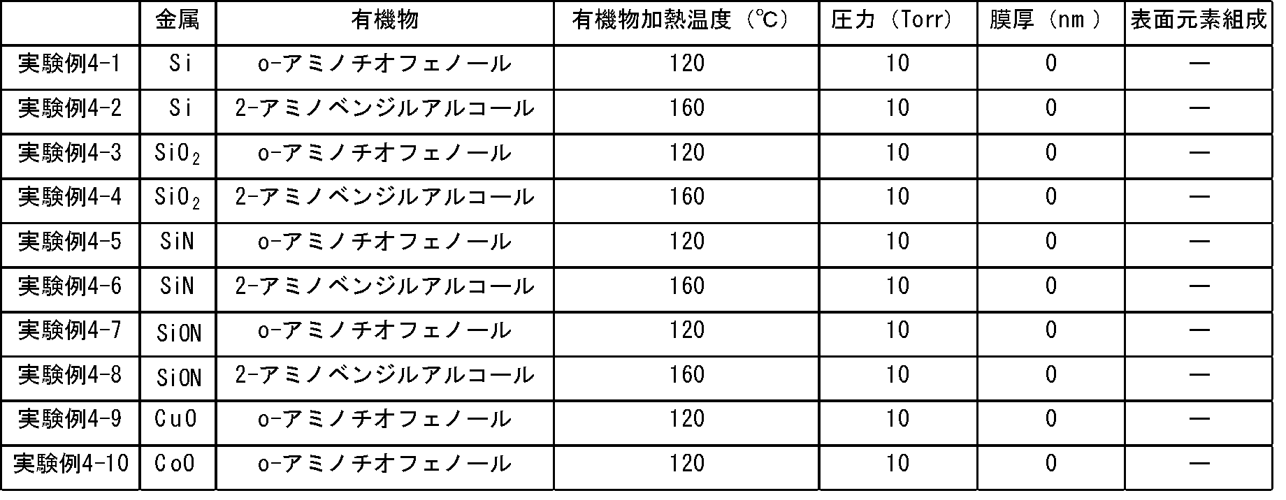
- Example 4-1 The substrate containing the Si surface was set in a chamber capable of performing a vacuum process, and the chamber pressure was set to 10 Torr. Next, the cylinder of o-aminothiophenol connected to the chamber was heated to 120 ° C. to open the valve, gas of o-aminothiophenol was supplied into the chamber, and the organic substance was placed on the substrate containing the Si surface. The film was deposited. After deposition of the organic film, the pressure inside the chamber was reduced to 0.1 Torr to remove excess organic material. When the film thickness of the organic substance formed on the substrate was measured by AFM, it was 0 nm. When the elemental composition was analyzed by XPS, nitrogen and sulfur peaks could not be confirmed.
- the substrate containing the Cu surface was prepared by forming a copper film with a thickness of about 100 nm on a silicon substrate by vapor deposition and then removing the surface natural oxide film.
- the substrate containing the Co surface was prepared by forming a cobalt film with a thickness of about 100 nm on a silicon substrate by vapor deposition and then removing the surface natural oxide film.
- the substrate containing the Ru surface was prepared by forming a ruthenium film with a thickness of about 100 nm on a silicon substrate by vapor deposition and then removing the surface natural oxide film.
- the substrate containing the Si surface was prepared by removing the natural oxide film of the silicon substrate.
- the substrate containing the SiO 2 surface was prepared by forming a silicon dioxide film to a thickness of about 30 nm on a silicon substrate by a chemical vapor deposition method.
- the substrate containing the SiN surface was manufactured by forming a silicon nitride film represented by a chemical formula of Si 3 N 4 to a thickness of about 30 nm on a silicon substrate by a chemical vapor deposition method.
- the substrate containing the SiON surface is oxidized after forming a SiN surface on the silicon substrate by a chemical vapor deposition method, and then Si 4 O x N y (x is 3 or more and 6 or less, y is 2 or more and 4 or less)
- the silicon oxynitride film represented by the chemical formula was formed to a thickness of about 10 nm.
- the substrate containing the CuO surface was produced by depositing a copper oxide film with a thickness of about 100 nm on a silicon substrate by vapor deposition.
- the substrate containing the CoO surface was produced by depositing a cobalt oxide film with a thickness of about 100 nm on a silicon substrate by vapor deposition.
- the organic material represented by the general formula (1) includes Ni, Pt, Al, Ta, Ti, and Hf, which are conductive materials suitable as wiring materials and electrode materials for semiconductor devices in addition to Co, Cu, and Ru. Films can also be deposited on metals such as.
Landscapes
- Chemical & Material Sciences (AREA)
- Engineering & Computer Science (AREA)
- Materials Engineering (AREA)
- Organic Chemistry (AREA)
- Life Sciences & Earth Sciences (AREA)
- Wood Science & Technology (AREA)
- Chemical Kinetics & Catalysis (AREA)
- Mechanical Engineering (AREA)
- Metallurgy (AREA)
- Chemical Vapour Deposition (AREA)
- Other Surface Treatments For Metallic Materials (AREA)
- Electrodes Of Semiconductors (AREA)
Abstract
Description

(1)
(一般式(1)において、Nは窒素原子であり、Xは酸素原子又は硫黄原子である。
R1は、炭素数2~12のヘテロ原子やハロゲン原子を有していてもよい炭化水素基であり、R2、R3、R4は、それぞれ独立して、水素原子又は炭素数1~10の環やヘテロ原子やハロゲン原子を有していてもよい炭化水素基である。但し、この炭化水素基は、炭素数が3以上の場合にあっては、分岐鎖あるいは環状構造の炭化水素基も含む。)

(1)
(一般式(1)においてNは窒素原子であり、Xは酸素原子又は硫黄原子である。
R1は、炭素数2~12のヘテロ原子やハロゲン原子を有していてもよい炭化水素基であり、R2、R3、R4は水素原子又は炭素数1~10の環やヘテロ原子やハロゲン原子を有していてもよい炭化水素基である。但し、上記炭化水素基は、炭素数が3以上の場合にあっては、分岐鎖あるいは環状構造の炭化水素基も含む。)
基板上に選択的に堆積した下記一般式(1)で表されることを特徴とする有機物の堆積膜である。

(1)
(一般式(1)においてNは窒素原子であり、Xは酸素原子又は硫黄原子である。
R1は炭素数2~12のヘテロ原子やハロゲン原子を有していてもよい炭化水素基であり、R2、R3、R4は水素原子又は炭素数1~10の環やヘテロ原子やハロゲン原子を有していてもよい炭化水素基である。但し、この炭化水素基は、炭素数が3以上の場合にあっては、分岐鎖あるいは環状構造の炭化水素基も含む。)

(1)
(一般式(1)においてNは窒素原子であり、Xは酸素原子又は硫黄原子である。
R1は炭素数2~12のヘテロ原子やハロゲン原子を有していてもよい炭化水素基であり、R2、R3、R4は水素原子又は炭素数1~10の環やヘテロ原子やハロゲン原子を有していてもよい炭化水素基である。但し、この炭化水素基は、炭素数が3以上の場合にあっては、分岐鎖あるいは環状構造の炭化水素基も含む。)
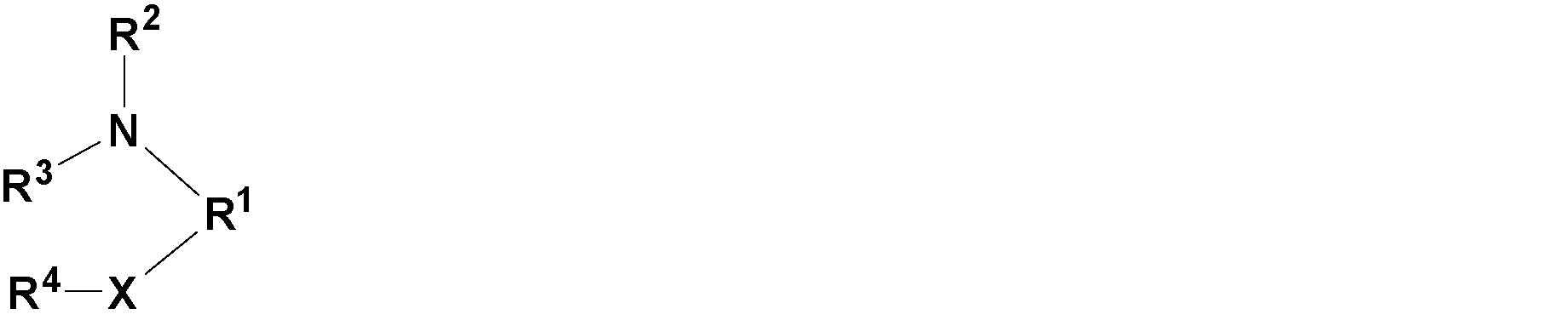
(一般式(1)においてNは窒素原子であり、Xは酸素原子又は硫黄原子である。
R1は炭素数2~12のヘテロ原子やハロゲン原子を有していてもよい炭化水素基であり、R2、R3、R4は水素原子又は炭素数1~10の環やヘテロ原子やハロゲン原子を有していてもよい炭化水素基である。但し、この炭化水素基は、炭素数が3以上の場合にあっては、分岐鎖あるいは環状構造の炭化水素基も含む。)
上記シリコンは、多結晶シリコンと単結晶シリコンの両方を含む。シリコン酸化物はSiOx(xは1以上2以下)の化学式で表され、通常はSiO2である。また、シリコン窒化物はSiNx(xは0.3以上9以下)の化学式で表され、通常はSi3N4である。シリコン酸窒化物はSi4OxNy(xは3以上6以下、yは2以上4以下)で表され、例えばSi4O5N3である。
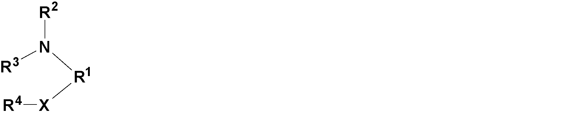
(1)
(一般式(1)においてNは窒素原子であり、Xは酸素原子または硫黄原子である。
R1は、炭素数2~12のヘテロ原子やハロゲン原子を有していてもよい炭化水素基であり、R2、R3、R4は、それぞれ独立して、水素原子又は炭素数1~10の環やヘテロ原子やハロゲン原子を有していてもよい炭化水素基である。但し、炭化水素基は、炭素数が3以上の場合にあっては、分岐鎖あるいは環状構造の炭化水素基も含む。)
R2、R3、R4としては、水素基やCH3、C2H5、C3H7等の炭化水素基等が挙げられる。R2、R3、R4を構成する炭化水素基の一部は、ヒドロキシ基、チオール基、アミノ基、ハロゲン等で置換されていてもよい。
更に、R3とR4が共に炭素数1以上の場合、R3とR4とが直接結合して、一般式(1)が環状構造をとっても良い。R2、R3、R4は、同じ置換基である場合もあるし、異なる置換基である場合もある。
本開示の実施の形態に係る湿式法では、上記した有機物と溶媒とを含む溶液に基板を暴露するが、その一例として、有機物と溶媒とを含む溶液に、第一表面領域と第二表面領域とを有する基板を浸漬することにより、上記基板の表面と上記溶液とを接触させ、有機物の膜を、基板の第一表面領域に選択的に堆積させる膜堆積工程を行うことができる。溶液に基板を暴露する方法として、浸漬法以外に、基板に溶液を滴下した後に高速回転させるスピンコート法や、溶液を基板に噴霧するスプレーコート法を用いることもできる。
本開示の実施の形態に係る乾式法では、有機物の気体を含む雰囲気に前記基板を暴露するが、具体的には、チャンバ内に基板を載置し、有機物を含む気体をチャンバ内に導入することにより、有機物を含む気体を基板の表面と接触させ、有機物の膜を、基板の第一表面領域に選択的に堆積させる膜堆積工程を行う。
本開示の基板は、金属を含む第一表面領域と、非金属無機材料及び/又は金属酸化物を含む第二表面領域とが両方とも露出した構造を持つ基板であって、上記第一表面領域に下記一般式(1)で表される有機物の膜を有し、上記第二表面領域に上記有機物の膜を有しないか、上記第二表面領域上の上記有機物の膜の厚さt2が、上記第一表面領域上の上記有機物の膜の厚さt1よりも薄いことを特徴とする。

(1)
(一般式(1)においてNは窒素原子であり、Xは酸素原子又は硫黄原子である。
R1は炭素数2~12のヘテロ原子やハロゲン原子を有していてもよい炭化水素基であり、R2、R3、R4は水素原子又は炭素数1~10の環やヘテロ原子やハロゲン原子を有していてもよい炭化水素基である。但し、上記炭化水素基は、炭素数が3以上の場合にあっては、分岐鎖あるいは環状構造の炭化水素基も含む。)
イソプロピルアルコール(以下、IPAという)に1%のo-アミノチオフェノールを溶解させ、有機物としてo-アミノチオフェノールと溶媒とを含む溶液を調製した。
次に、この溶液にCu表面を含有する基板を60秒浸漬させ、有機物の膜を堆積させた。溶液の温度は20~25℃であった。その後、20~25℃のIPAの液に60秒、2回浸漬させて、余分な有機物の除去を行い、続いて、20~25℃の窒素ガスを60秒間吹き付けて基板を乾燥させた。
基板上に形成された有機物の膜厚を原子間力顕微鏡(AFM)で測定したところ、48nmであった。また、X線光電子分光法(XPS)で元素組成を解析したところ、窒素と硫黄の強いピークを確認した。
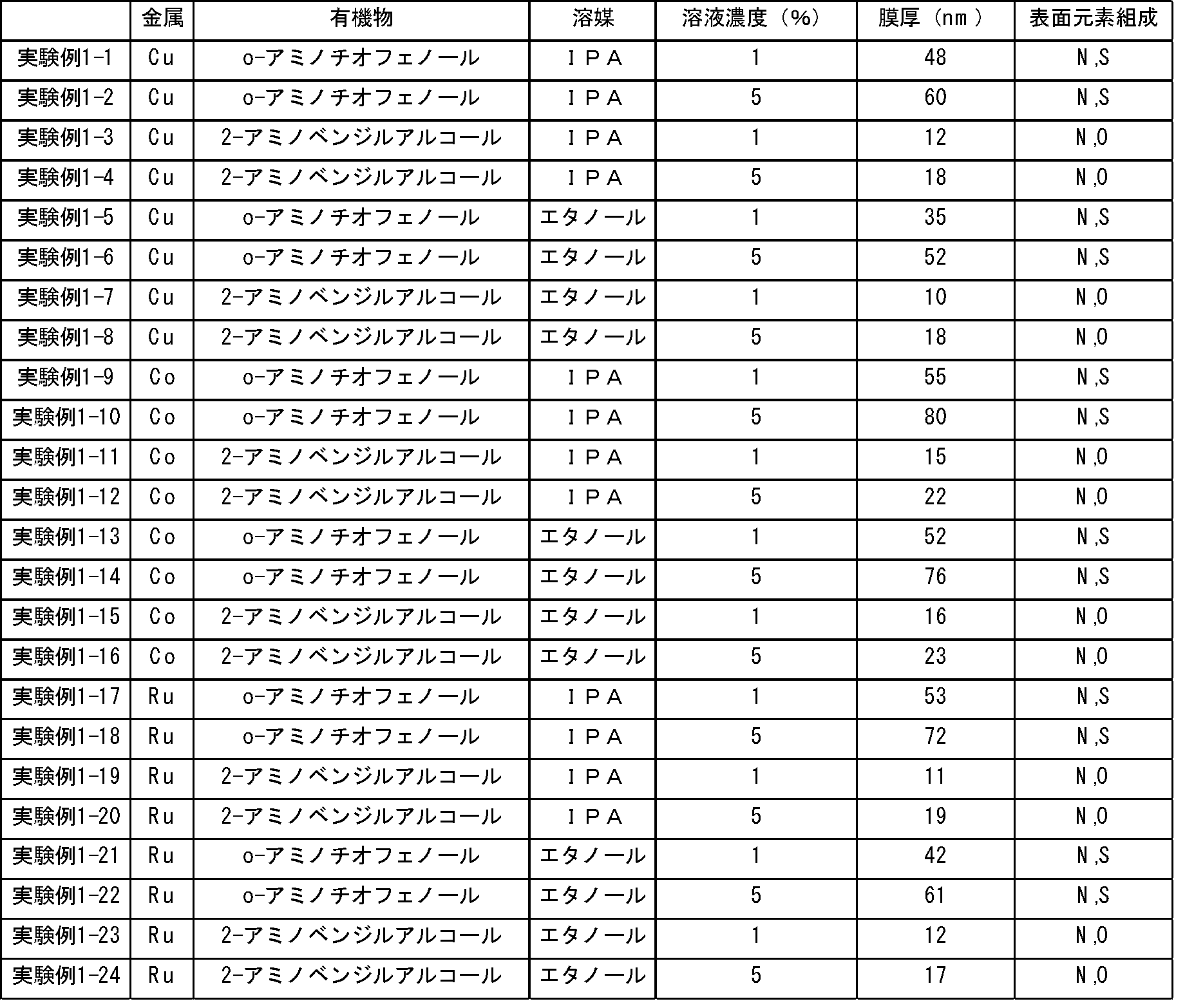
基板表面の金属、有機物の種類、溶媒の種類、溶液濃度などを、表1に示したように変更した以外は、実験例1-1と同様に実施し、評価を行った。その結果を表1に示す。
IPAに5%のo-アミノチオフェノールを溶解させ、有機物としてo-アミノチオフェノールと溶媒とを含む溶液を調製した。
次に、この溶液にSi表面を含有する基板を60秒浸漬させ、有機物の膜を堆積させた。溶液の温度は20~25℃であった。その後、20~25℃のIPAの液に60秒、2回浸漬させて、余分な有機物の除去を行い、20~25℃の窒素ガスを60秒間吹き付けて基板を乾燥させた。
基板上に形成された有機物の膜厚をAFMで測定したところ、0nmであった。また、XPSで元素組成を解析したところ、窒素と硫黄のピークは確認できなかった。
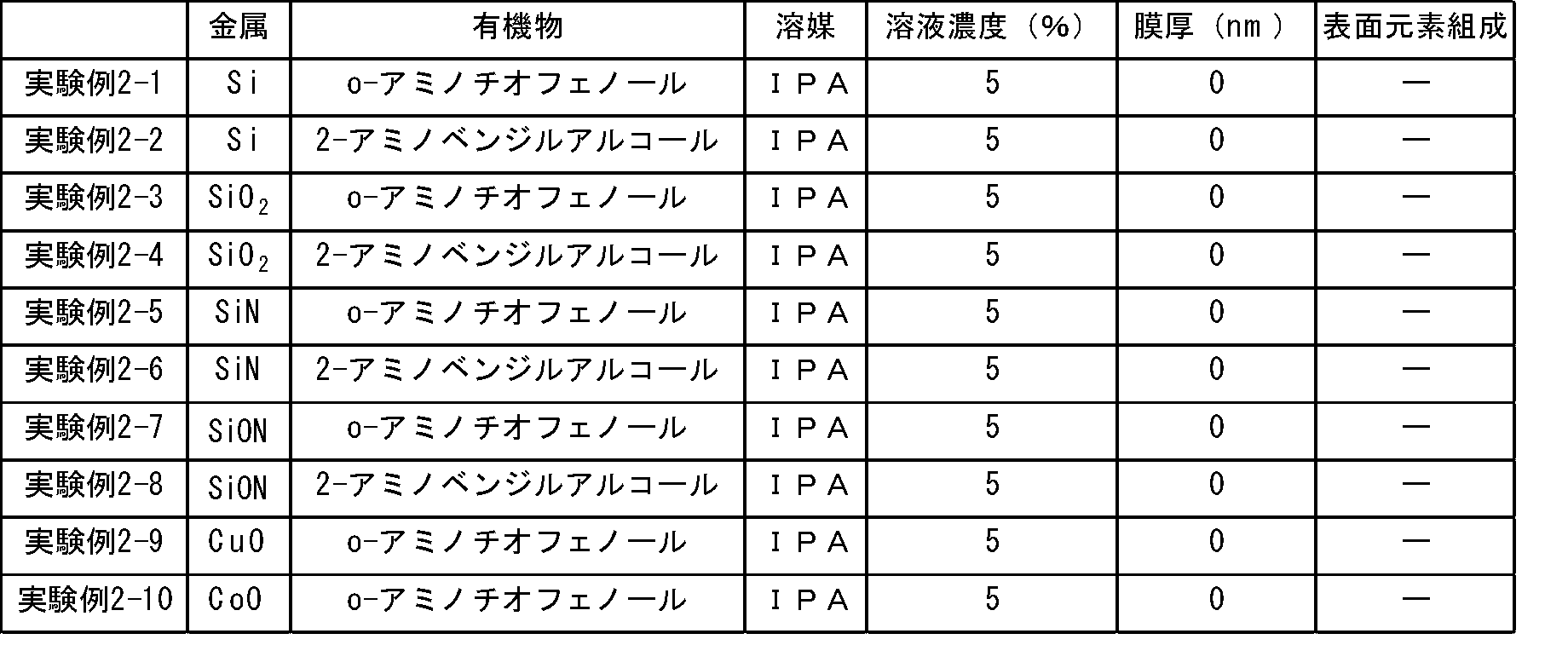
基板表面の金属、有機物の種類、溶媒の種類、溶液濃度などを、表2に示したように変更した以外は、実験例2-1と同様に実施し、評価を行った。その結果を表2に示す。
真空プロセスが可能なチャンバ内にCu表面を含有する基板をセットし、チャンバ圧力を1Torr(0.13kPa、絶対圧)に設定した。次に、チャンバに接続したo-アミノチオフェノールのシリンダーを80℃に加熱してバルブを解放し、o-アミノチオフェノールの気体をチャンバ内に供給し、Cuを含有する基板上に有機物の膜を堆積させた。なお、チャンバの温度は、シリンダーの温度と同じにし、o-アミノチオフェノールの気体の温度は、基板に接触するまで、シリンダーを保温する温度と同じに保たれるようにした。有機物の膜の堆積後、チャンバ内を0.1Torr(13Pa)に減圧して余分な有機物を除去した。
基板上に形成された有機物の膜厚をAFMで測定したところ、10nmであった。また、XPSで元素組成を解析したところ、窒素と硫黄の強いピークを確認した。
基板上の金属、有機物の種類、シリンダーを保温する温度(有機物加熱温度)、チャンバ圧力などを表3に示したように変更した以外は、実験例3-1と同様に実施し、評価を行った。その結果を表3に示す。
真空プロセスが可能なチャンバ内にSi表面を含有する基板をセットし、チャンバ圧力を10Torrに設定した。次に、チャンバに接続したo-アミノチオフェノールのシリンダーを120℃に加熱してバルブを解放し、o-アミノチオフェノールの気体をチャンバ内に供給し、Si表面を含有する基板上に有機物の膜を堆積させた。有機物の膜の堆積後、チャンバ内を0.1Torrに減圧して余分な有機物を除去した。
基板上に形成された有機物の膜厚をAFMで測定したところ、0nmであった。また、XPSで元素組成を解析したところ、窒素と硫黄のピークは確認できなかった。
基板上の金属、有機物の種類、シリンダーを保温する温度、チャンバ圧力などを表4に示したように変更した以外は、実験例4-1と同様に実施し、評価を行った。その結果を表4に示す。
Co表面を含有する基板は、蒸着によりシリコン基板上にコバルトの膜を厚さ約100nmで成膜した後、表面自然酸化膜を除去することにより作製した。
Ru表面を含有する基板は、蒸着によりシリコン基板上にルテニウムの膜を厚さ約100nmで成膜した後、表面自然酸化膜を除去することにより作製した。
SiO2表面を含有する基板は、化学的気相堆積法によりシリコン基板上に二酸化シリコンの膜を厚さ約30nmで成膜することにより作製した。
SiN表面を含有する基板は、化学的気相堆積法によりシリコン基板上にSi3N4の化学式で表される窒化シリコン膜を厚さ約30nmで成膜することにより作製した。
SiON表面を含有する基板は、化学的気相堆積法によりシリコン基板上にSiN表面を形成させた後に酸化してSi4OxNy(xは3以上6以下、yは2以上4以下)の化学式で表される酸窒化シリコン膜を厚さ約10nmで成膜することにより作製した。
CuO表面を含有する基板は、蒸着によりシリコン基板上に酸化銅の膜を厚さ約100nmで成膜することにより作製した。
CoO表面を含有する基板は、蒸着によりシリコン基板上に酸化コバルトの膜を厚さ約100nmで成膜することにより作製した。

Claims (18)
- 金属を含む第一表面領域と、非金属無機材料及び/又は金属酸化物を含む第二表面領域とが両方とも露出した構造を持つ基板に対して、
前記第二表面領域よりも前記第一表面領域に、下記一般式(1)で表される有機物の膜を選択的に堆積させることを特徴とする方法。

(一般式(1)において、Nは窒素原子であり、Xは酸素原子又は硫黄原子である。
R1は、炭素数2~12のヘテロ原子やハロゲン原子を有していてもよい炭化水素基であり、R2、R3及びR4は、それぞれ独立して、水素原子又は炭素数1~10の環やヘテロ原子やハロゲン原子を有していてもよい炭化水素基である。但し、この炭化水素基は、炭素数が3以上の場合にあっては、分岐鎖あるいは環状構造の炭化水素基も含む。) - 前記金属は、Cu、Co、Ru、Ni、Pt、Al、Ta、Ti及びHfからなる群より選ばれる少なくとも一つである、請求項1に記載の方法。
- 前記非金属無機材料は、シリコン、シリコン酸化物、シリコン窒化物及びシリコン酸窒化物からなる群から選ばれる少なくとも一つである、請求項1又は2に記載の方法。
- 前記金属酸化物は、Cu、Co、Ru、Ni、Pt、Al、Ta、Ti及びHfからなる群より選ばれる少なくとも一つの金属の酸化物である、請求項1~3のいずれか1項に記載の方法。
- 前記一般式(1)において、R2、R3及びR4は、水素原子である、請求項1~4のいずれか1項に記載の方法。
- 前記有機物は、o-アミノチオフェノール、2-アミノベンジルアルコール、2-アミノエタノール、2-(エチルアミノ)エタノール、2-アミノエタンチオール、3-アミノ-1-プロパノール及びo-アミノフェノールからなる群から選ばれる少なくとも一つである、請求項1に記載の方法。
- 前記第二表面領域よりも前記第一表面領域に有機物の膜を選択的に堆積させる工程は、前記有機物と溶媒とを含む溶液に前記基板を暴露する工程である、請求項1~6のいずれか1項に記載の方法。
- 前記溶液は、有機物と溶媒の合計に対して0.1質量%以上10質量%以下の前記一般式(1)で表される有機物を含む、請求項7に記載の方法。
- 前記基板に対して、前記一般式(1)で表される有機物の膜を選択的に堆積させた後、前記基板を溶媒で洗浄する、請求項7又は8に記載の方法。
- 前記第二表面領域よりも前記第一表面領域に、前記一般式(1)で表される有機物の膜を選択的に堆積させる工程が、前記有機物の気体を含む雰囲気に前記基板を暴露する工程である、請求項1~6のいずれか1項に記載の方法。
- 前記雰囲気の温度範囲は、0℃以上200℃以下である請求項10に記載の方法。
- 前記雰囲気の圧力範囲は、13Pa以上67kPa以下である請求項10又は11に記載の方法。
- 前記第一表面領域上の有機物の膜の厚さt1と、前期第二表面領域上の有機物の膜の厚さt2との比(t1/t2)が5以上である、請求項1~12のいずれか1項に記載の方法。
- 金属を含む第一表面領域と、非金属無機材料及び/又は金属酸化物を含む第二表面領域とが両方とも露出した構造を持つ基板であって、
前記第一表面領域に下記一般式(1)で表される有機物の膜を有し、
前記第二表面領域に前記有機物の膜を有しないか、前記第二表面領域上の前記有機物の膜の厚さt2が、前記第一表面領域上の前記有機物の膜の厚さt1よりも薄いことを特徴とする基板。
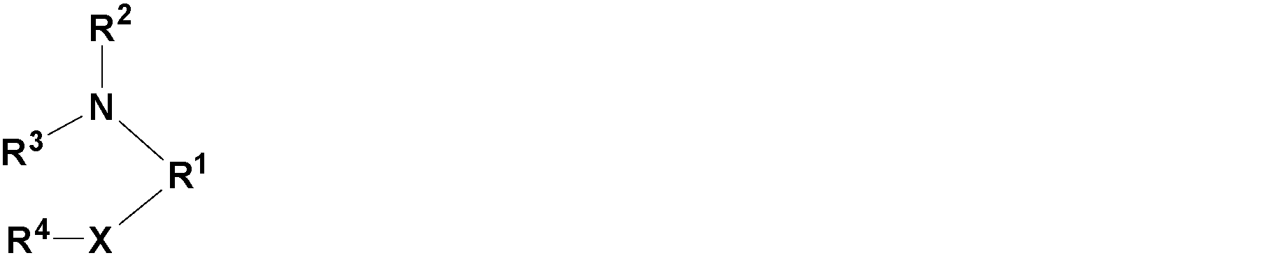
(一般式(1)においてNは窒素原子であり、Xは酸素原子又は硫黄原子である。
R1は炭素数2~12のヘテロ原子やハロゲン原子を有していてもよい炭化水素基であり、R2、R3、R4は水素原子又は炭素数1~10の環やヘテロ原子やハロゲン原子を有していてもよい炭化水素基である。但し、この炭化水素基は、炭素数が3以上の場合にあっては、分岐鎖あるいは環状構造の炭化水素基も含む。) - 請求項1~13のいずれか1項に記載された方法により形成された有機物の膜であって、
基板上に選択的に堆積した下記一般式(1)で表されることを特徴とする有機物の堆積膜。
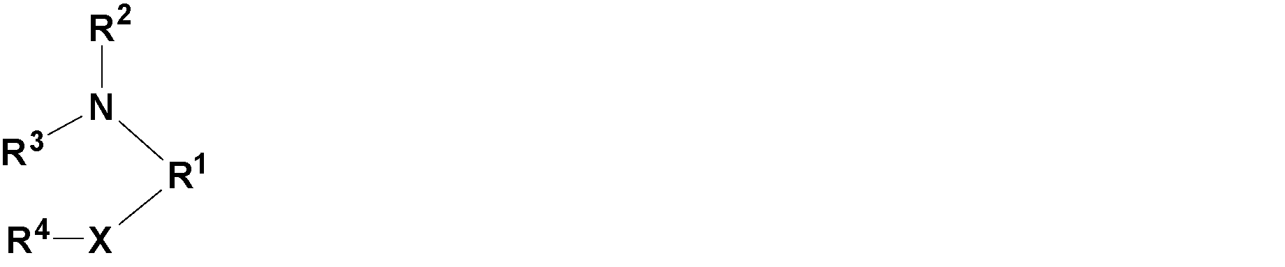
(一般式(1)においてNは窒素原子であり、Xは酸素原子又は硫黄原子である。
R1は炭素数2~12のヘテロ原子やハロゲン原子を有していてもよい炭化水素基であり、R2、R3、R4は水素原子又は炭素数1~10の環やヘテロ原子やハロゲン原子を有していてもよい炭化水素基である。但し、この炭化水素基は、炭素数が3以上の場合にあっては、分岐鎖あるいは環状構造の炭化水素基も含む。) - 請求項1~13のいずれか1項に記載された方法に用いることを特徴とする下記一般式(1)で表されることを特徴とする有機物。
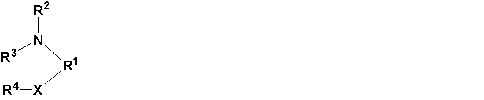
(一般式(1)においてNは窒素原子であり、Xは酸素原子又は硫黄原子である。
R1は炭素数2~12のヘテロ原子やハロゲン原子を有していてもよい炭化水素基であり、R2、R3、R4は水素原子又は炭素数1~10の環やヘテロ原子やハロゲン原子を有していてもよい炭化水素基である。但し、この炭化水素基は、炭素数が3以上の場合にあっては、分岐鎖あるいは環状構造の炭化水素基も含む。) - 下記一般式(1)で表されることを特徴とする有機物と、溶媒とを含むことを特徴とする溶液。

(一般式(1)においてNは窒素原子であり、Xは酸素原子又は硫黄原子である。
R1は炭素数2~12のヘテロ原子やハロゲン原子を有していてもよい炭化水素基であり、R2、R3、R4は水素原子又は炭素数1~10の環やヘテロ原子やハロゲン原子を有していてもよい炭化水素基である。但し、この炭化水素基は、炭素数が3以上の場合にあっては、分岐鎖あるいは環状構造の炭化水素基も含む。) - 前記有機物が、o-アミノチオフェノール、2-アミノベンジルアルコール、2-アミノエタノール、2-(エチルアミノ)エタノール、2-アミノエタンチオール、3-アミノ-1-プロパノール及びo-アミノフェノールからなる群から選ばれる少なくとも一つであり、
前記溶媒が、エタノール及びイソプロピルアルコールからなる群から選ばれる少なくとも一つであり、
前記溶液は、有機物と溶媒の合計に対して0.1質量%以上10質量%以下の前記一般式(1)で表される有機物を含む、ことを特徴とする請求項17に記載の溶液。
Priority Applications (2)
| Application Number | Priority Date | Filing Date | Title |
|---|---|---|---|
| JP2020528845A JP7303447B2 (ja) | 2018-07-02 | 2019-07-01 | 基板、基板の金属表面領域への選択的な膜堆積方法、有機物の堆積膜及び有機物 |
| KR1020207031516A KR102743163B1 (ko) | 2018-07-02 | 2019-07-01 | 기판, 기판의 금속표면영역에 대한 선택적인 막 퇴적방법, 유기물의 퇴적막 및 유기물 |
Applications Claiming Priority (2)
| Application Number | Priority Date | Filing Date | Title |
|---|---|---|---|
| JP2018126082 | 2018-07-02 | ||
| JP2018-126082 | 2018-07-02 |
Publications (1)
| Publication Number | Publication Date |
|---|---|
| WO2020009048A1 true WO2020009048A1 (ja) | 2020-01-09 |
Family
ID=69059680
Family Applications (1)
| Application Number | Title | Priority Date | Filing Date |
|---|---|---|---|
| PCT/JP2019/026014 Ceased WO2020009048A1 (ja) | 2018-07-02 | 2019-07-01 | 基板、基板の金属表面領域への選択的な膜堆積方法、有機物の堆積膜及び有機物 |
Country Status (4)
| Country | Link |
|---|---|
| JP (1) | JP7303447B2 (ja) |
| KR (1) | KR102743163B1 (ja) |
| TW (1) | TWI827630B (ja) |
| WO (1) | WO2020009048A1 (ja) |
Cited By (2)
| Publication number | Priority date | Publication date | Assignee | Title |
|---|---|---|---|---|
| WO2020145269A1 (ja) * | 2019-01-10 | 2020-07-16 | セントラル硝子株式会社 | 基板、選択的膜堆積方法、有機物の堆積膜及び有機物 |
| JP2022100079A (ja) * | 2020-12-23 | 2022-07-05 | 東京応化工業株式会社 | 表面処理剤、表面処理方法及び基板表面の領域選択的製膜方法 |
Citations (2)
| Publication number | Priority date | Publication date | Assignee | Title |
|---|---|---|---|---|
| JP2001189296A (ja) * | 1999-12-28 | 2001-07-10 | Nec Corp | 金属配線形成方法 |
| JP2017021014A (ja) * | 2012-02-07 | 2017-01-26 | ヴィブラント ホールディングス リミテッド ライアビリティ カンパニー | 基板、ペプチドアレイ、および方法 |
Family Cites Families (7)
| Publication number | Priority date | Publication date | Assignee | Title |
|---|---|---|---|---|
| JP3866811B2 (ja) | 1996-12-27 | 2007-01-10 | 松下電器産業株式会社 | 単分子膜およびその製造方法 |
| TWI627192B (zh) | 2015-03-13 | 2018-06-21 | Murata Manufacturing Co., Ltd. | 原子層堆積抑制材料 |
| US10453701B2 (en) | 2016-06-01 | 2019-10-22 | Asm Ip Holding B.V. | Deposition of organic films |
| US10373820B2 (en) * | 2016-06-01 | 2019-08-06 | Asm Ip Holding B.V. | Deposition of organic films |
| TWI647328B (zh) * | 2016-06-02 | 2019-01-11 | 美樺興業股份有限公司 | 選擇性抑制有機鍍膜形成的方法與選擇性調整有機鍍膜厚度的方法 |
| WO2018012545A1 (ja) * | 2016-07-15 | 2018-01-18 | 日東電工株式会社 | 表面保護フィルム、及び、光学部材 |
| US11094535B2 (en) | 2017-02-14 | 2021-08-17 | Asm Ip Holding B.V. | Selective passivation and selective deposition |
-
2019
- 2019-07-01 KR KR1020207031516A patent/KR102743163B1/ko active Active
- 2019-07-01 WO PCT/JP2019/026014 patent/WO2020009048A1/ja not_active Ceased
- 2019-07-01 JP JP2020528845A patent/JP7303447B2/ja active Active
- 2019-07-02 TW TW108123239A patent/TWI827630B/zh active
Patent Citations (2)
| Publication number | Priority date | Publication date | Assignee | Title |
|---|---|---|---|---|
| JP2001189296A (ja) * | 1999-12-28 | 2001-07-10 | Nec Corp | 金属配線形成方法 |
| JP2017021014A (ja) * | 2012-02-07 | 2017-01-26 | ヴィブラント ホールディングス リミテッド ライアビリティ カンパニー | 基板、ペプチドアレイ、および方法 |
Cited By (3)
| Publication number | Priority date | Publication date | Assignee | Title |
|---|---|---|---|---|
| WO2020145269A1 (ja) * | 2019-01-10 | 2020-07-16 | セントラル硝子株式会社 | 基板、選択的膜堆積方法、有機物の堆積膜及び有機物 |
| JP2022100079A (ja) * | 2020-12-23 | 2022-07-05 | 東京応化工業株式会社 | 表面処理剤、表面処理方法及び基板表面の領域選択的製膜方法 |
| JP7720694B2 (ja) | 2020-12-23 | 2025-08-08 | 東京応化工業株式会社 | 表面処理剤、表面処理方法及び基板表面の領域選択的製膜方法 |
Also Published As
| Publication number | Publication date |
|---|---|
| JP7303447B2 (ja) | 2023-07-05 |
| TWI827630B (zh) | 2024-01-01 |
| JPWO2020009048A1 (ja) | 2021-08-02 |
| KR102743163B1 (ko) | 2024-12-16 |
| KR20210029142A (ko) | 2021-03-15 |
| TW202012680A (zh) | 2020-04-01 |
Similar Documents
| Publication | Publication Date | Title |
|---|---|---|
| US10777411B1 (en) | Semiconductor device with selective dielectric deposition | |
| US9976037B2 (en) | Composition for treating surface of substrate, method and device | |
| US8614437B2 (en) | Organic underlayers that improve the performance of organic semiconductors | |
| CN113272471B (zh) | 基板、选择性膜沉积方法、有机物的沉积膜及有机物 | |
| JP7464539B2 (ja) | 共形性炭素膜堆積 | |
| US20170154975A1 (en) | Graphene transistor and related methods | |
| KR20210009284A (ko) | 표면 처리제, 표면 처리 방법 및 기판 표면의 영역 선택적 제막 방법 | |
| JP7303447B2 (ja) | 基板、基板の金属表面領域への選択的な膜堆積方法、有機物の堆積膜及び有機物 | |
| JP7638072B2 (ja) | 表面処理剤、表面処理方法及び基板表面の領域選択的製膜方法 | |
| US8871601B2 (en) | Diffusion barriers | |
| KR101723769B1 (ko) | 그래핀의 직접 전사 방법 및 그래핀층 상의 선택적 원자층 증착 방법 | |
| JP7804195B2 (ja) | 基板、選択的膜堆積方法、有機物の堆積膜及び有機物 | |
| CN120380574A (zh) | 基板处理液 | |
| US12601047B2 (en) | Substrate processing method and selective deposition method using the same | |
| TW202244053A (zh) | 表面處理劑、表面處理方法及基板表面之領域選擇性製膜方法 | |
| US12595564B2 (en) | Method of forming surface treatment film | |
| TWI922029B (zh) | 在半導體基板上沉積氧化矽薄膜的方法以及包括該方法的半導體裝置的製備方法 | |
| JP2021105196A (ja) | 表面処理剤、表面処理方法及び基板表面の領域選択的製膜方法 | |
| TWI922030B (zh) | 在半導體基板上沉積氧化矽薄膜的方法以及包括該方法的半導體裝置的製備方法 | |
| TW202526075A (zh) | 在半導體基板上沉積氧化矽薄膜的方法以及包括該方法的半導體裝置的製備方法 | |
| KR20230139306A (ko) | 기판 처리 방법 및 이를 사용한 선택적 증착 방법 | |
| CN119133056A (zh) | 自对准结构及其制备方法、半导体器件 | |
| TW200810164A (en) | Method of fabricating a electrical device |
Legal Events
| Date | Code | Title | Description |
|---|---|---|---|
| 121 | Ep: the epo has been informed by wipo that ep was designated in this application |
Ref document number: 19830012 Country of ref document: EP Kind code of ref document: A1 |
|
| ENP | Entry into the national phase |
Ref document number: 2020528845 Country of ref document: JP Kind code of ref document: A |
|
| ENP | Entry into the national phase |
Ref document number: 20207031516 Country of ref document: KR Kind code of ref document: A |
|
| NENP | Non-entry into the national phase |
Ref country code: DE |
|
| 122 | Ep: pct application non-entry in european phase |
Ref document number: 19830012 Country of ref document: EP Kind code of ref document: A1 |