WO2020008299A1 - 表示装置および電子機器 - Google Patents
表示装置および電子機器 Download PDFInfo
- Publication number
- WO2020008299A1 WO2020008299A1 PCT/IB2019/055325 IB2019055325W WO2020008299A1 WO 2020008299 A1 WO2020008299 A1 WO 2020008299A1 IB 2019055325 W IB2019055325 W IB 2019055325W WO 2020008299 A1 WO2020008299 A1 WO 2020008299A1
- Authority
- WO
- WIPO (PCT)
- Prior art keywords
- transistor
- electrode
- circuit
- display device
- light
- Prior art date
- Legal status (The legal status is an assumption and is not a legal conclusion. Google has not performed a legal analysis and makes no representation as to the accuracy of the status listed.)
- Ceased
Links
Images


Classifications
-
- G—PHYSICS
- G09—EDUCATION; CRYPTOGRAPHY; DISPLAY; ADVERTISING; SEALS
- G09G—ARRANGEMENTS OR CIRCUITS FOR CONTROL OF INDICATING DEVICES USING STATIC MEANS TO PRESENT VARIABLE INFORMATION
- G09G3/00—Control arrangements or circuits, of interest only in connection with visual indicators other than cathode-ray tubes
- G09G3/20—Control arrangements or circuits, of interest only in connection with visual indicators other than cathode-ray tubes for presentation of an assembly of a number of characters, e.g. a page, by composing the assembly by combination of individual elements arranged in a matrix no fixed position being assigned to or needed to be assigned to the individual characters or partial characters
- G09G3/34—Control arrangements or circuits, of interest only in connection with visual indicators other than cathode-ray tubes for presentation of an assembly of a number of characters, e.g. a page, by composing the assembly by combination of individual elements arranged in a matrix no fixed position being assigned to or needed to be assigned to the individual characters or partial characters by control of light from an independent source
- G09G3/36—Control arrangements or circuits, of interest only in connection with visual indicators other than cathode-ray tubes for presentation of an assembly of a number of characters, e.g. a page, by composing the assembly by combination of individual elements arranged in a matrix no fixed position being assigned to or needed to be assigned to the individual characters or partial characters by control of light from an independent source using liquid crystals
-
- G—PHYSICS
- G09—EDUCATION; CRYPTOGRAPHY; DISPLAY; ADVERTISING; SEALS
- G09G—ARRANGEMENTS OR CIRCUITS FOR CONTROL OF INDICATING DEVICES USING STATIC MEANS TO PRESENT VARIABLE INFORMATION
- G09G3/00—Control arrangements or circuits, of interest only in connection with visual indicators other than cathode-ray tubes
- G09G3/20—Control arrangements or circuits, of interest only in connection with visual indicators other than cathode-ray tubes for presentation of an assembly of a number of characters, e.g. a page, by composing the assembly by combination of individual elements arranged in a matrix no fixed position being assigned to or needed to be assigned to the individual characters or partial characters
- G09G3/22—Control arrangements or circuits, of interest only in connection with visual indicators other than cathode-ray tubes for presentation of an assembly of a number of characters, e.g. a page, by composing the assembly by combination of individual elements arranged in a matrix no fixed position being assigned to or needed to be assigned to the individual characters or partial characters using controlled light sources
- G09G3/30—Control arrangements or circuits, of interest only in connection with visual indicators other than cathode-ray tubes for presentation of an assembly of a number of characters, e.g. a page, by composing the assembly by combination of individual elements arranged in a matrix no fixed position being assigned to or needed to be assigned to the individual characters or partial characters using controlled light sources using electroluminescent panels
- G09G3/32—Control arrangements or circuits, of interest only in connection with visual indicators other than cathode-ray tubes for presentation of an assembly of a number of characters, e.g. a page, by composing the assembly by combination of individual elements arranged in a matrix no fixed position being assigned to or needed to be assigned to the individual characters or partial characters using controlled light sources using electroluminescent panels semiconductive, e.g. using light-emitting diodes [LED]
- G09G3/3208—Control arrangements or circuits, of interest only in connection with visual indicators other than cathode-ray tubes for presentation of an assembly of a number of characters, e.g. a page, by composing the assembly by combination of individual elements arranged in a matrix no fixed position being assigned to or needed to be assigned to the individual characters or partial characters using controlled light sources using electroluminescent panels semiconductive, e.g. using light-emitting diodes [LED] organic, e.g. using organic light-emitting diodes [OLED]
- G09G3/3225—Control arrangements or circuits, of interest only in connection with visual indicators other than cathode-ray tubes for presentation of an assembly of a number of characters, e.g. a page, by composing the assembly by combination of individual elements arranged in a matrix no fixed position being assigned to or needed to be assigned to the individual characters or partial characters using controlled light sources using electroluminescent panels semiconductive, e.g. using light-emitting diodes [LED] organic, e.g. using organic light-emitting diodes [OLED] using an active matrix
- G09G3/3233—Control arrangements or circuits, of interest only in connection with visual indicators other than cathode-ray tubes for presentation of an assembly of a number of characters, e.g. a page, by composing the assembly by combination of individual elements arranged in a matrix no fixed position being assigned to or needed to be assigned to the individual characters or partial characters using controlled light sources using electroluminescent panels semiconductive, e.g. using light-emitting diodes [LED] organic, e.g. using organic light-emitting diodes [OLED] using an active matrix with pixel circuitry controlling the current through the light-emitting element
-
- G—PHYSICS
- G02—OPTICS
- G02F—OPTICAL DEVICES OR ARRANGEMENTS FOR THE CONTROL OF LIGHT BY MODIFICATION OF THE OPTICAL PROPERTIES OF THE MEDIA OF THE ELEMENTS INVOLVED THEREIN; NON-LINEAR OPTICS; FREQUENCY-CHANGING OF LIGHT; OPTICAL LOGIC ELEMENTS; OPTICAL ANALOGUE/DIGITAL CONVERTERS
- G02F1/00—Devices or arrangements for the control of the intensity, colour, phase, polarisation or direction of light arriving from an independent light source, e.g. switching, gating or modulating; Non-linear optics
- G02F1/01—Devices or arrangements for the control of the intensity, colour, phase, polarisation or direction of light arriving from an independent light source, e.g. switching, gating or modulating; Non-linear optics for the control of the intensity, phase, polarisation or colour
- G02F1/13—Devices or arrangements for the control of the intensity, colour, phase, polarisation or direction of light arriving from an independent light source, e.g. switching, gating or modulating; Non-linear optics for the control of the intensity, phase, polarisation or colour based on liquid crystals, e.g. single liquid crystal display cells
- G02F1/133—Constructional arrangements; Operation of liquid crystal cells; Circuit arrangements
- G02F1/136—Liquid crystal cells structurally associated with a semi-conducting layer or substrate, e.g. cells forming part of an integrated circuit
- G02F1/1362—Active matrix addressed cells
- G02F1/1368—Active matrix addressed cells in which the switching element is a three-electrode device
-
- G—PHYSICS
- G09—EDUCATION; CRYPTOGRAPHY; DISPLAY; ADVERTISING; SEALS
- G09F—DISPLAYING; ADVERTISING; SIGNS; LABELS OR NAME-PLATES; SEALS
- G09F9/00—Indicating arrangements for variable information in which the information is built-up on a support by selection or combination of individual elements
- G09F9/30—Indicating arrangements for variable information in which the information is built-up on a support by selection or combination of individual elements in which the desired character or characters are formed by combining individual elements
-
- G—PHYSICS
- G09—EDUCATION; CRYPTOGRAPHY; DISPLAY; ADVERTISING; SEALS
- G09G—ARRANGEMENTS OR CIRCUITS FOR CONTROL OF INDICATING DEVICES USING STATIC MEANS TO PRESENT VARIABLE INFORMATION
- G09G3/00—Control arrangements or circuits, of interest only in connection with visual indicators other than cathode-ray tubes
- G09G3/20—Control arrangements or circuits, of interest only in connection with visual indicators other than cathode-ray tubes for presentation of an assembly of a number of characters, e.g. a page, by composing the assembly by combination of individual elements arranged in a matrix no fixed position being assigned to or needed to be assigned to the individual characters or partial characters
- G09G3/22—Control arrangements or circuits, of interest only in connection with visual indicators other than cathode-ray tubes for presentation of an assembly of a number of characters, e.g. a page, by composing the assembly by combination of individual elements arranged in a matrix no fixed position being assigned to or needed to be assigned to the individual characters or partial characters using controlled light sources
- G09G3/30—Control arrangements or circuits, of interest only in connection with visual indicators other than cathode-ray tubes for presentation of an assembly of a number of characters, e.g. a page, by composing the assembly by combination of individual elements arranged in a matrix no fixed position being assigned to or needed to be assigned to the individual characters or partial characters using controlled light sources using electroluminescent panels
- G09G3/32—Control arrangements or circuits, of interest only in connection with visual indicators other than cathode-ray tubes for presentation of an assembly of a number of characters, e.g. a page, by composing the assembly by combination of individual elements arranged in a matrix no fixed position being assigned to or needed to be assigned to the individual characters or partial characters using controlled light sources using electroluminescent panels semiconductive, e.g. using light-emitting diodes [LED]
- G09G3/3208—Control arrangements or circuits, of interest only in connection with visual indicators other than cathode-ray tubes for presentation of an assembly of a number of characters, e.g. a page, by composing the assembly by combination of individual elements arranged in a matrix no fixed position being assigned to or needed to be assigned to the individual characters or partial characters using controlled light sources using electroluminescent panels semiconductive, e.g. using light-emitting diodes [LED] organic, e.g. using organic light-emitting diodes [OLED]
- G09G3/3225—Control arrangements or circuits, of interest only in connection with visual indicators other than cathode-ray tubes for presentation of an assembly of a number of characters, e.g. a page, by composing the assembly by combination of individual elements arranged in a matrix no fixed position being assigned to or needed to be assigned to the individual characters or partial characters using controlled light sources using electroluminescent panels semiconductive, e.g. using light-emitting diodes [LED] organic, e.g. using organic light-emitting diodes [OLED] using an active matrix
-
- G—PHYSICS
- G09—EDUCATION; CRYPTOGRAPHY; DISPLAY; ADVERTISING; SEALS
- G09G—ARRANGEMENTS OR CIRCUITS FOR CONTROL OF INDICATING DEVICES USING STATIC MEANS TO PRESENT VARIABLE INFORMATION
- G09G3/00—Control arrangements or circuits, of interest only in connection with visual indicators other than cathode-ray tubes
- G09G3/20—Control arrangements or circuits, of interest only in connection with visual indicators other than cathode-ray tubes for presentation of an assembly of a number of characters, e.g. a page, by composing the assembly by combination of individual elements arranged in a matrix no fixed position being assigned to or needed to be assigned to the individual characters or partial characters
- G09G3/22—Control arrangements or circuits, of interest only in connection with visual indicators other than cathode-ray tubes for presentation of an assembly of a number of characters, e.g. a page, by composing the assembly by combination of individual elements arranged in a matrix no fixed position being assigned to or needed to be assigned to the individual characters or partial characters using controlled light sources
- G09G3/30—Control arrangements or circuits, of interest only in connection with visual indicators other than cathode-ray tubes for presentation of an assembly of a number of characters, e.g. a page, by composing the assembly by combination of individual elements arranged in a matrix no fixed position being assigned to or needed to be assigned to the individual characters or partial characters using controlled light sources using electroluminescent panels
- G09G3/32—Control arrangements or circuits, of interest only in connection with visual indicators other than cathode-ray tubes for presentation of an assembly of a number of characters, e.g. a page, by composing the assembly by combination of individual elements arranged in a matrix no fixed position being assigned to or needed to be assigned to the individual characters or partial characters using controlled light sources using electroluminescent panels semiconductive, e.g. using light-emitting diodes [LED]
- G09G3/3208—Control arrangements or circuits, of interest only in connection with visual indicators other than cathode-ray tubes for presentation of an assembly of a number of characters, e.g. a page, by composing the assembly by combination of individual elements arranged in a matrix no fixed position being assigned to or needed to be assigned to the individual characters or partial characters using controlled light sources using electroluminescent panels semiconductive, e.g. using light-emitting diodes [LED] organic, e.g. using organic light-emitting diodes [OLED]
- G09G3/3275—Details of drivers for data electrodes
-
- G—PHYSICS
- G09—EDUCATION; CRYPTOGRAPHY; DISPLAY; ADVERTISING; SEALS
- G09G—ARRANGEMENTS OR CIRCUITS FOR CONTROL OF INDICATING DEVICES USING STATIC MEANS TO PRESENT VARIABLE INFORMATION
- G09G3/00—Control arrangements or circuits, of interest only in connection with visual indicators other than cathode-ray tubes
- G09G3/20—Control arrangements or circuits, of interest only in connection with visual indicators other than cathode-ray tubes for presentation of an assembly of a number of characters, e.g. a page, by composing the assembly by combination of individual elements arranged in a matrix no fixed position being assigned to or needed to be assigned to the individual characters or partial characters
- G09G3/34—Control arrangements or circuits, of interest only in connection with visual indicators other than cathode-ray tubes for presentation of an assembly of a number of characters, e.g. a page, by composing the assembly by combination of individual elements arranged in a matrix no fixed position being assigned to or needed to be assigned to the individual characters or partial characters by control of light from an independent source
- G09G3/36—Control arrangements or circuits, of interest only in connection with visual indicators other than cathode-ray tubes for presentation of an assembly of a number of characters, e.g. a page, by composing the assembly by combination of individual elements arranged in a matrix no fixed position being assigned to or needed to be assigned to the individual characters or partial characters by control of light from an independent source using liquid crystals
- G09G3/3611—Control of matrices with row and column drivers
- G09G3/3648—Control of matrices with row and column drivers using an active matrix
-
- G—PHYSICS
- G09—EDUCATION; CRYPTOGRAPHY; DISPLAY; ADVERTISING; SEALS
- G09G—ARRANGEMENTS OR CIRCUITS FOR CONTROL OF INDICATING DEVICES USING STATIC MEANS TO PRESENT VARIABLE INFORMATION
- G09G3/00—Control arrangements or circuits, of interest only in connection with visual indicators other than cathode-ray tubes
- G09G3/20—Control arrangements or circuits, of interest only in connection with visual indicators other than cathode-ray tubes for presentation of an assembly of a number of characters, e.g. a page, by composing the assembly by combination of individual elements arranged in a matrix no fixed position being assigned to or needed to be assigned to the individual characters or partial characters
- G09G3/34—Control arrangements or circuits, of interest only in connection with visual indicators other than cathode-ray tubes for presentation of an assembly of a number of characters, e.g. a page, by composing the assembly by combination of individual elements arranged in a matrix no fixed position being assigned to or needed to be assigned to the individual characters or partial characters by control of light from an independent source
- G09G3/36—Control arrangements or circuits, of interest only in connection with visual indicators other than cathode-ray tubes for presentation of an assembly of a number of characters, e.g. a page, by composing the assembly by combination of individual elements arranged in a matrix no fixed position being assigned to or needed to be assigned to the individual characters or partial characters by control of light from an independent source using liquid crystals
- G09G3/3611—Control of matrices with row and column drivers
- G09G3/3685—Details of drivers for data electrodes
- G09G3/3688—Details of drivers for data electrodes suitable for active matrices only
-
- H—ELECTRICITY
- H05—ELECTRIC TECHNIQUES NOT OTHERWISE PROVIDED FOR
- H05B—ELECTRIC HEATING; ELECTRIC LIGHT SOURCES NOT OTHERWISE PROVIDED FOR; CIRCUIT ARRANGEMENTS FOR ELECTRIC LIGHT SOURCES, IN GENERAL
- H05B33/00—Electroluminescent light sources
- H05B33/12—Light sources with substantially two-dimensional radiating surfaces
- H05B33/14—Light sources with substantially two-dimensional radiating surfaces characterised by the chemical or physical composition or the arrangement of the electroluminescent material, or by the simultaneous addition of the electroluminescent material in or onto the light source
-
- H—ELECTRICITY
- H10—SEMICONDUCTOR DEVICES; ELECTRIC SOLID-STATE DEVICES NOT OTHERWISE PROVIDED FOR
- H10D—INORGANIC ELECTRIC SEMICONDUCTOR DEVICES
- H10D30/00—Field-effect transistors [FET]
- H10D30/60—Insulated-gate field-effect transistors [IGFET]
- H10D30/67—Thin-film transistors [TFT]
-
- H—ELECTRICITY
- H10—SEMICONDUCTOR DEVICES; ELECTRIC SOLID-STATE DEVICES NOT OTHERWISE PROVIDED FOR
- H10D—INORGANIC ELECTRIC SEMICONDUCTOR DEVICES
- H10D30/00—Field-effect transistors [FET]
- H10D30/60—Insulated-gate field-effect transistors [IGFET]
- H10D30/67—Thin-film transistors [TFT]
- H10D30/674—Thin-film transistors [TFT] characterised by the active materials
- H10D30/6755—Oxide semiconductors, e.g. zinc oxide, copper aluminium oxide or cadmium stannate
-
- H—ELECTRICITY
- H10—SEMICONDUCTOR DEVICES; ELECTRIC SOLID-STATE DEVICES NOT OTHERWISE PROVIDED FOR
- H10D—INORGANIC ELECTRIC SEMICONDUCTOR DEVICES
- H10D86/00—Integrated devices formed in or on insulating or conducting substrates, e.g. formed in silicon-on-insulator [SOI] substrates or on stainless steel or glass substrates
- H10D86/40—Integrated devices formed in or on insulating or conducting substrates, e.g. formed in silicon-on-insulator [SOI] substrates or on stainless steel or glass substrates characterised by multiple TFTs
- H10D86/421—Integrated devices formed in or on insulating or conducting substrates, e.g. formed in silicon-on-insulator [SOI] substrates or on stainless steel or glass substrates characterised by multiple TFTs having a particular composition, shape or crystalline structure of the active layer
- H10D86/423—Integrated devices formed in or on insulating or conducting substrates, e.g. formed in silicon-on-insulator [SOI] substrates or on stainless steel or glass substrates characterised by multiple TFTs having a particular composition, shape or crystalline structure of the active layer comprising semiconductor materials not belonging to the Group IV, e.g. InGaZnO
-
- H—ELECTRICITY
- H10—SEMICONDUCTOR DEVICES; ELECTRIC SOLID-STATE DEVICES NOT OTHERWISE PROVIDED FOR
- H10D—INORGANIC ELECTRIC SEMICONDUCTOR DEVICES
- H10D86/00—Integrated devices formed in or on insulating or conducting substrates, e.g. formed in silicon-on-insulator [SOI] substrates or on stainless steel or glass substrates
- H10D86/40—Integrated devices formed in or on insulating or conducting substrates, e.g. formed in silicon-on-insulator [SOI] substrates or on stainless steel or glass substrates characterised by multiple TFTs
- H10D86/60—Integrated devices formed in or on insulating or conducting substrates, e.g. formed in silicon-on-insulator [SOI] substrates or on stainless steel or glass substrates characterised by multiple TFTs wherein the TFTs are in active matrices
-
- H—ELECTRICITY
- H10—SEMICONDUCTOR DEVICES; ELECTRIC SOLID-STATE DEVICES NOT OTHERWISE PROVIDED FOR
- H10K—ORGANIC ELECTRIC SOLID-STATE DEVICES
- H10K50/00—Organic light-emitting devices
-
- H—ELECTRICITY
- H10—SEMICONDUCTOR DEVICES; ELECTRIC SOLID-STATE DEVICES NOT OTHERWISE PROVIDED FOR
- H10K—ORGANIC ELECTRIC SOLID-STATE DEVICES
- H10K59/00—Integrated devices, or assemblies of multiple devices, comprising at least one organic light-emitting element covered by group H10K50/00
-
- G—PHYSICS
- G09—EDUCATION; CRYPTOGRAPHY; DISPLAY; ADVERTISING; SEALS
- G09G—ARRANGEMENTS OR CIRCUITS FOR CONTROL OF INDICATING DEVICES USING STATIC MEANS TO PRESENT VARIABLE INFORMATION
- G09G2300/00—Aspects of the constitution of display devices
- G09G2300/04—Structural and physical details of display devices
- G09G2300/0421—Structural details of the set of electrodes
- G09G2300/0426—Layout of electrodes and connections
-
- G—PHYSICS
- G09—EDUCATION; CRYPTOGRAPHY; DISPLAY; ADVERTISING; SEALS
- G09G—ARRANGEMENTS OR CIRCUITS FOR CONTROL OF INDICATING DEVICES USING STATIC MEANS TO PRESENT VARIABLE INFORMATION
- G09G2300/00—Aspects of the constitution of display devices
- G09G2300/04—Structural and physical details of display devices
- G09G2300/0439—Pixel structures
- G09G2300/0465—Improved aperture ratio, e.g. by size reduction of the pixel circuit, e.g. for improving the pixel density or the maximum displayable luminance or brightness
-
- G—PHYSICS
- G09—EDUCATION; CRYPTOGRAPHY; DISPLAY; ADVERTISING; SEALS
- G09G—ARRANGEMENTS OR CIRCUITS FOR CONTROL OF INDICATING DEVICES USING STATIC MEANS TO PRESENT VARIABLE INFORMATION
- G09G2300/00—Aspects of the constitution of display devices
- G09G2300/08—Active matrix structure, i.e. with use of active elements, inclusive of non-linear two terminal elements, in the pixels together with light emitting or modulating elements
- G09G2300/0809—Several active elements per pixel in active matrix panels
-
- G—PHYSICS
- G09—EDUCATION; CRYPTOGRAPHY; DISPLAY; ADVERTISING; SEALS
- G09G—ARRANGEMENTS OR CIRCUITS FOR CONTROL OF INDICATING DEVICES USING STATIC MEANS TO PRESENT VARIABLE INFORMATION
- G09G2300/00—Aspects of the constitution of display devices
- G09G2300/08—Active matrix structure, i.e. with use of active elements, inclusive of non-linear two terminal elements, in the pixels together with light emitting or modulating elements
- G09G2300/088—Active matrix structure, i.e. with use of active elements, inclusive of non-linear two terminal elements, in the pixels together with light emitting or modulating elements using a non-linear two-terminal element
- G09G2300/0895—Active matrix structure, i.e. with use of active elements, inclusive of non-linear two terminal elements, in the pixels together with light emitting or modulating elements using a non-linear two-terminal element having more than one selection line for a two-terminal active matrix LCD, e.g. Lechner and D2R circuits
-
- G—PHYSICS
- G09—EDUCATION; CRYPTOGRAPHY; DISPLAY; ADVERTISING; SEALS
- G09G—ARRANGEMENTS OR CIRCUITS FOR CONTROL OF INDICATING DEVICES USING STATIC MEANS TO PRESENT VARIABLE INFORMATION
- G09G2310/00—Command of the display device
- G09G2310/02—Addressing, scanning or driving the display screen or processing steps related thereto
- G09G2310/0264—Details of driving circuits
- G09G2310/027—Details of drivers for data electrodes, the drivers handling digital grey scale data, e.g. use of D/A converters
-
- G—PHYSICS
- G09—EDUCATION; CRYPTOGRAPHY; DISPLAY; ADVERTISING; SEALS
- G09G—ARRANGEMENTS OR CIRCUITS FOR CONTROL OF INDICATING DEVICES USING STATIC MEANS TO PRESENT VARIABLE INFORMATION
- G09G2310/00—Command of the display device
- G09G2310/02—Addressing, scanning or driving the display screen or processing steps related thereto
- G09G2310/0264—Details of driving circuits
- G09G2310/0297—Special arrangements with multiplexing or demultiplexing of display data in the drivers for data electrodes, in a pre-processing circuitry delivering display data to said drivers or in the matrix panel, e.g. multiplexing plural data signals to one D/A converter or demultiplexing the D/A converter output to multiple columns
-
- G—PHYSICS
- G09—EDUCATION; CRYPTOGRAPHY; DISPLAY; ADVERTISING; SEALS
- G09G—ARRANGEMENTS OR CIRCUITS FOR CONTROL OF INDICATING DEVICES USING STATIC MEANS TO PRESENT VARIABLE INFORMATION
- G09G2310/00—Command of the display device
- G09G2310/08—Details of timing specific for flat panels, other than clock recovery
-
- G—PHYSICS
- G09—EDUCATION; CRYPTOGRAPHY; DISPLAY; ADVERTISING; SEALS
- G09G—ARRANGEMENTS OR CIRCUITS FOR CONTROL OF INDICATING DEVICES USING STATIC MEANS TO PRESENT VARIABLE INFORMATION
- G09G2320/00—Control of display operating conditions
- G09G2320/02—Improving the quality of display appearance
- G09G2320/0233—Improving the luminance or brightness uniformity across the screen
-
- H—ELECTRICITY
- H10—SEMICONDUCTOR DEVICES; ELECTRIC SOLID-STATE DEVICES NOT OTHERWISE PROVIDED FOR
- H10D—INORGANIC ELECTRIC SEMICONDUCTOR DEVICES
- H10D30/00—Field-effect transistors [FET]
- H10D30/60—Insulated-gate field-effect transistors [IGFET]
- H10D30/67—Thin-film transistors [TFT]
- H10D30/6729—Thin-film transistors [TFT] characterised by the electrodes
- H10D30/673—Thin-film transistors [TFT] characterised by the electrodes characterised by the shapes, relative sizes or dispositions of the gate electrodes
- H10D30/6733—Multi-gate TFTs
- H10D30/6734—Multi-gate TFTs having gate electrodes arranged on both top and bottom sides of the channel, e.g. dual-gate TFTs
-
- H—ELECTRICITY
- H10—SEMICONDUCTOR DEVICES; ELECTRIC SOLID-STATE DEVICES NOT OTHERWISE PROVIDED FOR
- H10K—ORGANIC ELECTRIC SOLID-STATE DEVICES
- H10K59/00—Integrated devices, or assemblies of multiple devices, comprising at least one organic light-emitting element covered by group H10K50/00
- H10K59/10—OLED displays
- H10K59/12—Active-matrix OLED [AMOLED] displays
- H10K59/121—Active-matrix OLED [AMOLED] displays characterised by the geometry or disposition of pixel elements
- H10K59/1213—Active-matrix OLED [AMOLED] displays characterised by the geometry or disposition of pixel elements the pixel elements being TFTs
-
- H—ELECTRICITY
- H10—SEMICONDUCTOR DEVICES; ELECTRIC SOLID-STATE DEVICES NOT OTHERWISE PROVIDED FOR
- H10K—ORGANIC ELECTRIC SOLID-STATE DEVICES
- H10K59/00—Integrated devices, or assemblies of multiple devices, comprising at least one organic light-emitting element covered by group H10K50/00
- H10K59/10—OLED displays
- H10K59/12—Active-matrix OLED [AMOLED] displays
- H10K59/131—Interconnections, e.g. wiring lines or terminals
Definitions
- One embodiment of the present invention relates to a display device.
- one embodiment of the present invention is not limited to the above technical field.
- the technical field of one embodiment of the present invention disclosed in this specification and the like relates to an object, a method, or a manufacturing method.
- one embodiment of the present invention relates to a process, a machine, a manufacture, or a composition (composition of matter). Therefore, more specifically, the technical field of one embodiment of the present invention disclosed in this specification includes a semiconductor device, a display device, a liquid crystal display device, a light-emitting device, a lighting device, a power storage device, a storage device, an imaging device, An operation method or a manufacturing method thereof can be given as an example.
- a semiconductor device in this specification and the like refers to all devices that can function by utilizing semiconductor characteristics.
- a transistor and a semiconductor circuit are one embodiment of a semiconductor device.
- the storage device, the display device, the imaging device, and the electronic device sometimes include a semiconductor device.
- Patent Literatures 1 and 2 disclose a technique in which a transistor using zinc oxide or an In—Ga—Zn-based oxide is used for a switching element of a pixel of a display device or the like.
- Patent Document 3 discloses a memory device having a structure in which a transistor with extremely low off-state current is used for a memory cell.
- a high-resolution display device capable of performing display at a resolution of 8K4K (the number of pixels: 7680 ⁇ 4320) or higher has been developed. Also, the introduction of HDR (high dynamic range) display technology for improving image quality by adjusting the brightness has been advanced.
- HDR high dynamic range
- the output voltage of a source driver for a liquid crystal display device is about 10 to 20 V, and a high-output source driver must be used to supply a higher voltage to a display device.
- a high-output source driver consumes high power, and a new driver IC may need to be developed.
- an object of one embodiment of the present invention is to provide a display device capable of improving image quality. Another object is to provide a display device which can supply a voltage higher than or equal to an output voltage of a source driver to a display device. Another object is to provide a display device capable of increasing luminance of a display image. Another object is to provide a display device which can increase the aperture ratio of a pixel.
- Another object is to provide a display device with low power consumption. Alternatively, another object is to provide a highly reliable display device. Another object is to provide a new display device or the like. Another object is to provide a method for driving the display device. Another object is to provide a novel semiconductor device or the like.
- One embodiment of the present invention relates to a display device capable of improving image quality.
- One embodiment of the present invention is a display device including a pixel and a first circuit, in which the pixel and the first circuit are electrically connected to each other. 2 has a function of adding the first data and the third data to generate the third data, and the pixel has a function of adding the first data and the third data to generate the fourth data. It is a display device having a function of performing display in response.
- Another embodiment of the present invention is a display device including a pixel and a first circuit, wherein the pixel is electrically connected to the first circuit, and the first circuit includes a first data And a function of adding third data to the third data to generate third data, and a function of adding third data to the third data to generate fourth data.
- This is a display device having a function of performing display according to data.
- the first circuit includes a first transistor, a second transistor, a third transistor, and a first capacitor, and one of a source and a drain of the first transistor is electrically connected to the pixel. And one of a source and a drain of the first transistor is electrically connected to one electrode of the first capacitor, and the other electrode of the first capacitor is connected to a source or drain of the second transistor. One of the source and the drain of the second transistor is electrically connected to one of the source and the drain of the third transistor, and the other of the source and the drain of the first transistor is connected to the first The second transistor can be electrically connected to the other of the source and the drain.
- the first capacitor has a plurality of second capacitors, and the second capacitors may be connected in parallel.
- the pixel includes a fourth transistor, a fifth transistor, a sixth transistor, a third capacitor, and a second circuit, and one of a source and a drain of the fourth transistor is connected to the fourth transistor.
- the third electrode is electrically connected to one electrode of the third capacitor, the one electrode of the third capacitor is electrically connected to the second circuit, and the other electrode of the third capacitor is connected to the fifth transistor.
- One of a source and a drain of the fifth transistor is electrically connected to one of a source and a drain, and one of a source and a drain of the fifth transistor is electrically connected to one of a source and a drain of the sixth transistor.
- the other is electrically connected to the first circuit, the other of the source and the drain of the fifth transistor is electrically connected to the first circuit, and the second circuit is electrically connected to the first circuit. You can have a device.
- the second circuit includes a seventh transistor, a fourth capacitor, and a light-emitting device as a display device.
- a gate of the seventh transistor is electrically connected to the other of the source and the drain of the fourth transistor.
- one of a source and a drain of the seventh transistor is electrically connected to one electrode of the light emitting device, and one electrode of the light emitting device is electrically connected to one electrode of the fourth capacitor.
- the other electrode of the fourth capacitor can be electrically connected to the gate of the seventh transistor.
- the second circuit may include a liquid crystal device as a display device, and one electrode of the liquid crystal device may be electrically connected to one of a source and a drain of the fourth transistor.
- the liquid crystal device may further include a fifth capacitor, and one electrode of the fifth capacitor may be electrically connected to one electrode of the liquid crystal device.
- the transistor included in the first circuit and the pixel includes a metal oxide in a channel formation region, and the metal oxide includes In, Zn, and M (M is Al, Ti, Ga, Sn, Y, Zr, or La. , Ce, Nd or Hf).
- the channel width of the transistor included in the first circuit be larger than the channel width of the transistor included in the pixel.
- a display device capable of improving image quality can be provided.
- a display device which can supply a voltage higher than or equal to an output voltage of a source driver to a display device can be provided.
- a display device capable of increasing the luminance of a display image can be provided.
- a display device capable of increasing the aperture ratio of a pixel can be provided.
- a display device with low power consumption can be provided.
- a highly reliable display device can be provided.
- a new display device or the like can be provided.
- an operation method of the display device can be provided.
- a novel semiconductor device or the like can be provided.
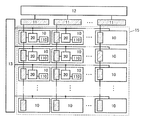
- FIG. 1 is a diagram illustrating a display device.
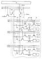
- FIG. 2 is a diagram illustrating an addition circuit and a pixel.
- FIGS. 3A to 3F are diagrams illustrating an adder circuit and a pixel.
- FIG. 4 is a diagram illustrating an addition circuit and a pixel.
- FIG. 5 is a timing chart illustrating the operation of the addition circuit and the pixel.
- FIG. 6 is a timing chart illustrating the operation of the addition circuit and the pixel.
- FIGS. 7A to 7D are diagrams illustrating circuit blocks.
- FIGS. 8A to 8D are diagrams illustrating circuit blocks.
- FIGS. 9A to 9C are diagrams illustrating circuit blocks.
- FIG. 10 is a diagram illustrating an addition circuit and a pixel.
- FIG. 11 is a diagram illustrating a configuration of an adder circuit and a pixel used for a simulation.
- FIG. 12 is a timing chart used for the simulation.
- FIG. 13 is a timing chart used for the simulation.
- FIG. 14 is a diagram illustrating the result of the simulation.
- FIG. 15 is a diagram illustrating the result of the simulation.
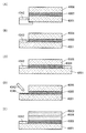
- FIGS. 16A to 16C are diagrams illustrating a display device.
- FIGS. 17A and 17B are diagrams illustrating a touch panel.
- FIGS. 18A and 18B are diagrams illustrating a display device.
- FIG. 19 is a diagram illustrating a display device.
- FIGS. 20A and 20B illustrate a display device.
- FIGS. 21A and 21B are diagrams illustrating a display device.
- FIGS. 22A to 22E are diagrams illustrating a display device.
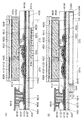
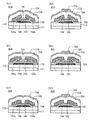
- FIGS. 23A1 to 23C2 illustrate a transistor.
- FIGS. 24A1 to 24C2 illustrate a transistor.
- FIGS. 25A1 to 25C2 are diagrams illustrating a transistor.
- FIGS. 26A1 to 26C2 illustrate a transistor.
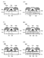
- FIGS. 27A to 27F are diagrams illustrating electronic devices.
- the element may be configured by a plurality of elements unless there is a functional inconvenience.
- a plurality of transistors operating as switches may be connected in series or in parallel.
- the capacitor may be divided and arranged at a plurality of positions.
- one conductor may have a plurality of functions such as a wiring, an electrode, and a terminal in some cases, and in this specification, a plurality of names may be used for the same element.
- a plurality of names may be used for the same element.
- the elements may actually be connected via a plurality of conductors in some cases. In this document, such a configuration is also included in the category of direct connection.
- One embodiment of the present invention is a display device including a circuit having a function of adding data (hereinafter, an addition circuit) and a pixel having a function of adding data.
- the addition circuit has a function of adding data supplied from the source driver.
- the pixel has a function of adding data supplied from the addition circuit. Therefore, the display device of one embodiment of the present invention can generate a voltage several times higher than the output voltage of the source driver and supply the generated voltage to the display device.
- the addition circuit is electrically connected to the pixels in the display area column direction, and some of the elements can be divided and arranged in the pixel area. Therefore, restrictions on the size of elements included in the addition circuit can be relaxed, and data can be added efficiently. In addition, by providing other elements included in the addition circuit outside the display region, the number of wirings in the display region can be reduced, and the aperture ratio can be increased in a pixel.
- FIG. 1 illustrates a display device of one embodiment of the present invention.
- the display device includes the pixels 10 arranged in the column direction and the row direction, a source driver 12, a gate driver 13, and a circuit 11.
- Source driver 12 is electrically connected to circuit 11.
- Gate driver 13 is electrically connected to pixel 10.
- the circuit 11 is electrically connected to the pixel 10.
- FIG. 1 shows an example in which one gate driver 13 is provided along one side of the display region 15, one more gate driver is provided along a side opposite to the one side, and a pixel driver is provided by two gate drivers. 10 may be driven.
- the circuit 11 can be provided for each column, and is electrically connected to all the pixels 10 arranged in the same column. Elements of the circuit 11 can be provided inside and outside the display area.
- the circuit 11 is an addition circuit, and has a function of adding first data and second data supplied from the source driver 12 by capacitive coupling to generate third data.
- the pixel 10 includes a circuit 20 and a circuit block 110.
- the circuit 20 has a function of adding the first data and the third data supplied from the adding circuit by capacitive coupling to generate fourth data. Alternatively, it has a function of adding the third data to the third data supplied from the adding circuit by capacitive coupling to generate fifth data.
- the circuit block 110 has a display device and has a function of performing display on the display device in accordance with the fourth data or the fifth data supplied from the circuit 20.
- FIG. 2 illustrates a circuit 11 and a pixel 10 (pixels 10 [m, 1] to 10 [m, n] (m and n are 1 or more) arranged in an arbitrary column (m-th column) of the display device illustrated in FIG. FIG.
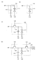
- the circuit 11 can have a structure including the transistor 101, the transistor 102, the transistor 103, and the capacitor 107.
- One of a source and a drain of the transistor 101 is electrically connected to one electrode of the capacitor 107.
- the other electrode of the capacitor 107 is electrically connected to one of a source and a drain of the transistor 102.
- One of a source and a drain of the transistor 102 is electrically connected to one electrode of the transistor 103.
- the capacitor 107 can be configured by connecting a plurality of capacitors 108 in parallel. By distributing the capacitors 108 in the pixel region, the total area of the capacitors 107 can be easily increased. Further, the area occupied by the circuit 11 outside the display area can be reduced, and the frame can be narrow. Note that some capacitors 108 may be provided outside the display area. Further, the capacitor 108 may not be provided in all pixel regions. By adjusting the number of capacitors 108 connected in parallel, the capacitance value of the capacitor 107 can be set to a desired value.
- the capacitor 108 can have the wiring 125 as one electrode and another wiring overlapping with the wiring 125 as the other electrode. Therefore, even if the capacitor 108 is arranged in the pixel region as shown in FIG. 2, the aperture ratio does not significantly decrease.
- the pixel 10 can have a configuration including the circuit 20 and the circuit block 110. Further, as described above, the capacitor 108 can be arranged in the pixel region.
- the circuit 20 can have a structure including the transistor 104, the transistor 105, the transistor 106, and the capacitor 109.
- One of a source and a drain of the transistor 104 is electrically connected to one electrode of the capacitor 109.
- the other electrode of the capacitor 109 is electrically connected to one of a source and a drain of the transistor 105.
- One of a source and a drain of the transistor 105 is electrically connected to one of a source and a drain of the transistor 106.
- One of a source and a drain of the transistor 104 is electrically connected to the circuit block 110.
- the circuit block 110 can be configured to include a transistor, a capacitor, a display device, and the like, and details will be described later.
- the gate of the transistor 101 is electrically connected to the wiring 121.
- the gate of the transistor 102 is electrically connected to the wiring 122.
- the gate of the transistor 103 is electrically connected to the wiring 121.
- the gate of the transistor 104 is electrically connected to the wiring 123.
- the gate of the transistor 105 is electrically connected to the wiring 124.
- the gate of the transistor 106 is electrically connected to the wiring 123.
- One of a source and a drain of the transistor 101 is electrically connected to the wiring 125.
- the other of the source and the drain of the transistor 101 and the other of the source and the drain of the transistor 102 are electrically connected to the wiring 126.
- the other of the source and the drain of the transistor 103 and the other of the source and the drain of the transistor 106 are electrically connected to a wiring which can supply V ref (for example, a reference potential such as 0 V).
- the wirings 121, 122, and 123 (123 [1] to [n]) and the wiring 124 (124 [1] to [n]) have functions as gate lines.
- the wirings 121 and 122 can be electrically connected to a circuit that controls operation of the circuit 11.
- the wirings 123 and 124 can be electrically connected to the gate driver 13.
- the wiring 126 can be electrically connected to the source driver 12 (see FIG. 1).
- a wiring (wiring 125) connecting one of the source and the drain of the transistor 101, one electrode of the capacitor 107, and one of the source and the drain of the transistor 105 is referred to as a node NA.
- a wiring connecting one of the source or the drain of the transistor 102, one of the source or the drain of the transistor 103, and the other electrode of the capacitor 107 is referred to as a node NB.
- a wiring connecting one of the source and the drain of the transistor 105, one of the source and the drain of the transistor 106, and the other electrode of the capacitor 109 is referred to as a node NC.
- a wiring connecting one of the source and the drain of the transistor 104, one electrode of the capacitor 109, and the circuit block 110 is referred to as a node NP.
- the node NP can be floating, and the display device included in the circuit block 110 operates according to the potential of the node NP.
- first data (weight: W) is written to the node NA.
- “V ref ” is supplied to the other electrode of the capacitor 107, and “W ⁇ V ref ” is held in the capacitor 107.
- the node NA is floated, and the second data (data: D) is supplied to the node NB.
- the potential of the node NA is W + (C 107 / (C 107 + C NA )) ⁇ (D ⁇ V ref ).
- the potential of the node NA becomes "W + D-V ref" .
- the potential of the node NP is W + (C 109 / (C 109 + C NP )) ⁇ (2D ⁇ V ref ).
- the potential of the node NP becomes "W + 2D-V ref" .
- the pixel 10 can perform an operation different from that described above.
- “2D” is written to the node NA.
- “V ref ” is supplied to the other electrode of the capacitor 109, and “2D ⁇ V ref ” is held in the capacitor 109.
- the node NP is set to the floating state, and the third data (“2D”) is supplied to the node NC.
- the potential of the node NP is 2D + (C 109 / (C 109 + C NP )) ⁇ (2D ⁇ V ref ).
- the potential of the node NP becomes "2D + 2D-V ref" .
- a high voltage can be generated even when a general-purpose driver IC is used.
- a liquid crystal device that requires a high voltage for gradation control can be driven.
- the voltage supplied from the source driver 12 for driving a general liquid crystal device or a light emitting device can be reduced to about 1/3 to 1/4, so that the power consumption of the display device can be reduced. .
- correction data may be supplied as the first data (weight: W).
- W the first data
- the threshold voltage correction data of the transistor is supplied as the first data (weight: W). Then, the display quality may be improved.
- the first data (weight: W) and the second data (data: D) may be interchanged.
- the data potential generated by the circuit 11 is supplied to the specific pixel 10 as described above to determine the potential of the node NP.
- the potential of the node NP of each pixel 10 can be determined. That is, different image data can be supplied to each pixel 10.
- the nodes NA, NB, NC, and NP act as storage nodes. Data can be written to each node by turning on a transistor connected to each node. In addition, by turning off the transistor, the data can be held at each node.
- a transistor with extremely low off-state current is used as the transistor, leakage current can be suppressed and the potential of each node can be held for a long time.
- a transistor including a metal oxide for a channel formation region hereinafter, referred to as an OS transistor
- an OS transistor can be used as the transistor.
- an OS transistor it is preferable to apply an OS transistor to any or all of the transistors 101, 102, 103, 104, 105, and 106. Further, an OS transistor may be applied to an element included in the circuit block 110. In the case where operation is performed in a range where the amount of leakage current is allowable, a transistor including Si in a channel formation region (hereinafter, a Si transistor) may be used. Alternatively, an OS transistor and a Si transistor may be used in combination. Note that examples of the Si transistor include a transistor including amorphous silicon, a transistor including crystalline silicon (microcrystalline silicon, low-temperature polysilicon, and single-crystal silicon).
- a metal oxide having an energy gap of 2 eV or more, preferably 2.5 eV or more, more preferably 3 eV or more can be used.
- an oxide semiconductor containing indium or the like is used; for example, a CAAC-OS or a CAC-OS described later can be used.
- the CAAC-OS has stable atoms in its crystal and is suitable for a transistor or the like in which reliability is emphasized.
- the CAC-OS has high mobility characteristics, it is suitable for a transistor that drives at high speed or the like.
- the OS transistor has an extremely low off-current characteristic of several yA / ⁇ m (current value per 1 ⁇ m of channel width) because the energy gap of the semiconductor layer is large. Further, the OS transistor has characteristics different from those of the Si transistor, such as being free from impact ionization, avalanche breakdown, and a short-channel effect, and can form a highly reliable circuit. In addition, variation in electrical characteristics due to non-uniformity of crystallinity, which is a problem in the Si transistor, hardly occurs in the OS transistor.
- the semiconductor layer included in the OS transistor includes an In-M-Zn-based oxide including, for example, indium, zinc, and M (a metal such as aluminum, titanium, gallium, germanium, yttrium, zirconium, lanthanum, cerium, tin, neodymium, or hafnium). Can be obtained.
- M a metal such as aluminum, titanium, gallium, germanium, yttrium, zirconium, lanthanum, cerium, tin, neodymium, or hafnium.
- the oxide semiconductor included in the semiconductor layer is an In-M-Zn-based oxide
- the atomic ratio of metal elements in a sputtering target used for forming the In-M-Zn oxide is In ⁇ M
- Zn It is preferable to satisfy ⁇ M.
- each of the atomic ratios of the semiconductor layers to be formed includes a variation of ⁇ 40% of the atomic ratio of the metal element contained in the sputtering target.
- the semiconductor layer an oxide semiconductor with low carrier density is used.
- the semiconductor layer has a carrier density of 1 ⁇ 10 17 / cm 3 or less, preferably 1 ⁇ 10 15 / cm 3 or less, further preferably 1 ⁇ 10 13 / cm 3 or less, more preferably 1 ⁇ 10 11 / cm 3. 3 or less, more preferably less than 1 ⁇ 10 10 / cm 3 , and an oxide semiconductor with a carrier density of 1 ⁇ 10 ⁇ 9 / cm 3 or more can be used.
- Such an oxide semiconductor is referred to as a highly purified intrinsic or substantially highly purified intrinsic oxide semiconductor. It can be said that the oxide semiconductor has a low density of defect states and has stable characteristics.
- the composition is not limited thereto, and a transistor having an appropriate composition may be used depending on required semiconductor characteristics and electric characteristics (eg, field-effect mobility and threshold voltage) of the transistor.
- the carrier density, the impurity concentration, the defect density, the atomic ratio between a metal element and oxygen, the interatomic distance, the density, and the like be appropriate.
- the concentration of silicon or carbon (concentration obtained by secondary ion mass spectrometry) in the semiconductor layer is set to 2 ⁇ 10 18 atoms / cm 3 or less, preferably 2 ⁇ 10 17 atoms / cm 3 or less.
- an alkali metal and an alkaline earth metal may generate carriers when combined with an oxide semiconductor, which may increase off-state current of a transistor. Therefore, the concentration of alkali metal or alkaline earth metal in the semiconductor layer (concentration obtained by secondary ion mass spectrometry) is 1 ⁇ 10 18 atoms / cm 3 or less, preferably 2 ⁇ 10 16 atoms / cm 3 or less.
- the nitrogen concentration (concentration obtained by secondary ion mass spectrometry) in the semiconductor layer is preferably 5 ⁇ 10 18 atoms / cm 3 or less.
- oxygen when hydrogen is contained in the oxide semiconductor included in the semiconductor layer, oxygen reacts with oxygen bonded to a metal atom to become water, so that oxygen vacancies may be formed in the oxide semiconductor in some cases.
- oxygen vacancies are contained in a channel formation region in an oxide semiconductor, the transistor might have normally-on characteristics.
- a defect in which hydrogen is contained in an oxygen vacancy functions as a donor, and an electron serving as a carrier may be generated.
- part of hydrogen is bonded to oxygen which is bonded to a metal atom to generate an electron serving as a carrier. Therefore, a transistor including an oxide semiconductor containing a large amount of hydrogen is likely to have normally-on characteristics.
- a defect in which hydrogen is contained in an oxygen vacancy can function as a donor of an oxide semiconductor.
- an oxide semiconductor is evaluated not by a donor concentration but by a carrier concentration. Therefore, in this specification and the like, a carrier concentration which assumes a state where an electric field is not applied may be used instead of a donor concentration as a parameter of an oxide semiconductor in some cases. That is, the “carrier concentration” described in this specification and the like may be referred to as a “donor concentration” in some cases.
- the hydrogen concentration obtained by secondary ion mass spectrometry is lower than 1 ⁇ 10 20 atoms / cm 3 , preferably 1 ⁇ 10 19 atoms / cm 3. It is less than 3 , more preferably less than 5 ⁇ 10 18 atoms / cm 3 , further preferably less than 1 ⁇ 10 18 atoms / cm 3 .
- an oxide semiconductor in which impurities such as hydrogen are sufficiently reduced is used for a channel formation region of a transistor, stable electric characteristics can be provided.
- the semiconductor layer may have a non-single-crystal structure, for example.
- the non-single-crystal structure includes, for example, a CAAC-OS (C-Axis Aligned Crystalline Oxide Semiconductor) having a crystal oriented in the c-axis, a polycrystalline structure, a microcrystalline structure, or an amorphous structure.
- CAAC-OS C-Axis Aligned Crystalline Oxide Semiconductor
- the amorphous structure has the highest density of defect states
- the CAAC-OS has the lowest density of defect states.
- An oxide semiconductor film having an amorphous structure has, for example, disordered atomic arrangement and no crystalline component.
- an oxide film having an amorphous structure has, for example, a completely amorphous structure and no crystal part.
- the semiconductor layer is a mixed film including two or more of an amorphous structure region, a microcrystalline structure region, a polycrystalline structure region, a CAAC-OS region, and a single crystal structure region.
- the mixed film may have a single-layer structure or a stacked structure including any two or more of the above-described regions, for example.
- CAC cloud-aligned composite
- the CAC-OS is one structure of a material in which an element included in an oxide semiconductor is unevenly distributed in a size of, for example, 0.5 nm or more and 10 nm or less, preferably, 1 nm or more and 2 nm or less.
- one or more metal elements are unevenly distributed in an oxide semiconductor, and a region including the metal element has a size of 0.5 nm to 10 nm, preferably 1 nm to 2 nm, or a size in the vicinity thereof.
- the state mixed by is also referred to as a mosaic shape or a patch shape.
- the oxide semiconductor preferably contains at least indium. In particular, it preferably contains indium and zinc.
- a CAC-OS in an In-Ga-Zn oxide is an indium oxide (hereinafter referred to as InO).
- X1 (X1 is greater real than 0) and.), or indium zinc oxide (hereinafter, in X2 Zn Y2 O Z2 ( X2, Y2, and Z2 is larger real than 0) and a.), gallium Oxide (hereinafter, referred to as GaO X3 (X3 is a real number larger than 0)) or gallium zinc oxide (hereinafter, Ga X4 Zn Y4 O Z4 (X4, Y4, and Z4 are real numbers larger than 0)) and to.) and the like, the material becomes mosaic by separate into, mosaic InO X1 or in X2 Zn Y2 O Z2, is a configuration in which uniformly distributed in the film (hereinafter Also referred to as a cloud-like.) A.
- the CAC-OS is a composite oxide semiconductor having a structure in which a region containing GaO X3 as a main component and a region containing In X2 Zn Y2 O Z2 or InO X1 as a main component are mixed.
- the atomic ratio of In to the element M in the first region is larger than the atomic ratio of In to the element M in the second region.
- the concentration of In is higher than that of the region No. 2.
- IGZO is a common name and may refer to one compound of In, Ga, Zn, and O. Representative examples are represented by InGaO 3 (ZnO) m1 (m1 is a natural number), or In (1 + x0) Ga ( 1-x0) O 3 (ZnO) m0 (-1 ⁇ x0 ⁇ 1, m0 is an arbitrary number) Crystalline compounds are mentioned.
- the above crystalline compound has a single crystal structure, a polycrystal structure, or a CAAC structure.
- the CAAC structure is a crystal structure in which a plurality of IGZO nanocrystals have a c-axis orientation and are connected without being oriented in the ab plane.
- CAC-OS relates to a material structure of an oxide semiconductor.
- CAC-OS is a material composition containing In, Ga, Zn, and O, a region which is observed in the form of a nanoparticle mainly containing Ga as a part and a nanoparticle mainly containing In as a part.
- a region observed in a shape refers to a configuration in which each region is randomly dispersed in a mosaic shape. Therefore, in the CAC-OS, the crystal structure is a secondary element.
- the CAC-OS does not include a stacked structure of two or more kinds of films having different compositions.
- a structure including two layers of a film mainly containing In and a film mainly containing Ga is not included.
- the CAC-OS is divided into a region which is observed in the form of a nanoparticle mainly including the metal element and a nanoparticle mainly including In.
- the region observed in the form of particles refers to a configuration in which each of the regions is randomly dispersed in a mosaic shape.
- the CAC-OS can be formed by, for example, a sputtering method under conditions in which the substrate is not heated intentionally.
- a sputtering method any one or more selected from an inert gas (typically, argon), an oxygen gas, and a nitrogen gas is used as a deposition gas.
- an inert gas typically, argon
- oxygen gas typically, argon
- a nitrogen gas is used as a deposition gas.
- the flow rate ratio of the oxygen gas to the total flow rate of the film formation gas during the film formation is preferably as low as possible.
- the flow rate ratio of the oxygen gas is preferably from 0% to less than 30%, more preferably from 0% to 10%. .
- the CAC-OS is characterized in that a clear peak is not observed when measured using a ⁇ / 2 ⁇ scan by an Out-of-plane method, which is one of X-ray diffraction (X-ray diffraction) measurement methods. Have. That is, from the X-ray diffraction measurement, it is understood that the orientation in the a-b plane direction and the c-axis direction of the measurement region is not observed.
- the CAC-OS includes, in an electron beam diffraction pattern obtained by irradiating an electron beam (also referred to as a nanobeam electron beam) having a probe diameter of 1 nm, a region (ring region) having a high luminance in a ring shape and the ring region. Multiple bright spots are observed in the area. Accordingly, the electron diffraction pattern shows that the crystal structure of the CAC-OS has an nc (nano-crystal) structure having no orientation in a planar direction and a cross-sectional direction.
- an electron beam also referred to as a nanobeam electron beam
- GaO X3 is a main component in EDX mapping obtained using energy dispersive X-ray spectroscopy (EDX: Energy Dispersive X-ray spectrum). It can be confirmed that the region and the region containing In X2 Zn Y2 O Z2 or InO X1 as a main component are unevenly distributed and mixed.
- the CAC-OS has a different structure from an IGZO compound in which metal elements are uniformly distributed, and has different properties from the IGZO compound. That is, the CAC-OS is phase-separated into a region containing GaO X3 or the like as a main component and a region containing In X2 Zn Y2 O Z2 or InO X1 as a main component. Has a mosaic structure.
- a region in which In X2 Zn Y2 O Z2 or InO X1 is a main component is a region having higher conductivity than a region in which GaO X3 or the like is a main component. That is, when a carrier flows through a region containing In X2 Zn Y2 O Z2 or InO X1 as a main component, conductivity as an oxide semiconductor is exhibited. Therefore, high field-effect mobility ( ⁇ ) can be realized by distributing a region containing In X2 Zn Y2 O Z2 or InO X1 as a main component in a cloud shape in the oxide semiconductor.
- a region containing GaO X3 or the like as a main component is a region having higher insulating properties than a region containing In X2 Zn Y2 O Z2 or InO X1 as a main component. That is, a region in which GaO X3 or the like is a main component is distributed in the oxide semiconductor, so that a leak current can be suppressed and a favorable switching operation can be realized.
- the insulating property caused by GaO X3 and the like and the conductivity caused by In X2 Zn Y2 O Z2 or InO X1 act complementarily, so that high performance is obtained.
- On-state current (I on ) and high field-effect mobility ( ⁇ ) can be realized.
- CAC-OS is suitable as a constituent material of various semiconductor devices.
- elements other than the capacitor 107 of the circuit 11 may be incorporated in the source driver 12 as illustrated in FIG. With this configuration, the frame can be narrowed.
- a stack structure having a region where any of the elements of the source driver 12 and the circuit 11 overlap may be employed. With this configuration, the degree of freedom in designing the elements of the circuit 11 can be increased, and the electrical characteristics can be improved.
- FIG. 1 shows an example in which the circuit 11 is provided for each column.
- a selection circuit 16 is provided between the circuit 11 and the pixel 10 to provide data for pixels in a plurality of columns. May be performed by one circuit 11.
- FIG. 3B illustrates an example in which writing is performed on pixels in three columns using a combination of one circuit 11 and one selection circuit 16; Then, the number of columns may be determined.
- the capacitor 107 may be provided outside the display region together with the circuit 11 without being provided in the display region.
- a stack structure including a region where the circuit 11 and the capacitor 107 overlap may be employed. With such a structure, the aperture ratio of the pixel 10 can be increased.
- the capacitor 107 may be incorporated in the source driver 12.
- a stack structure having a region where the source driver 12 and the capacitor 107 overlap may be employed. With this configuration, the frame can be narrowed.
- a configuration in which the capacitor 107 is arranged outside the display region and the circuit 11 is incorporated in the source driver 12 may be employed.
- a stack structure having an area where the source driver 12 and the circuit 11 overlap may be employed. With such a structure, it is possible to narrow the frame and increase the aperture ratio of the pixel.
- the circuit 11 and the capacitor 107 may be incorporated in the source driver 12.
- a stack structure having a region where the source driver 12 overlaps with any of the circuit 11 and the capacitor 107 may be employed.
- a stack structure having a region where the source driver 12, the circuit 11, and the capacitor 107 overlap with each other may be employed. With this configuration, the frame can be narrowed.
- the transistors 101, 102, and 103 included in the circuit 11 are provided outside the display region; therefore, the size of the transistors 101, 102, and 103 is hardly limited, and the channel width can be larger than that of a transistor provided in a pixel. With the use of a transistor with a large channel width, the charge and discharge time for the wiring 125 and the like can be reduced, and the frame frequency can be easily increased. Further, the present invention can be easily applied to a high definition display having a large number of pixels and a short horizontal period.
- the circuit 11 can have a high withstand voltage, and stable operation can be performed even when a voltage generated in addition of data is several tens of volts.
- the transistors 101, 102, and 103 are Si transistors provided in an IC chip, higher-speed operation can be performed. Note that when the transistors 101, 102, and 103 are provided in an IC chip, the transistors may be OS transistors.
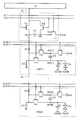
- the circuit 11 may be provided in both a region along one side of the display region 15 and a region along a side opposite to the one side, as shown in FIG.
- the circuit 11 provided on one side of the display area 15 is a circuit 11a.
- the operation of the circuit 11a is controlled by signals supplied from the wirings 121a and 122a.
- the circuit 11a is electrically connected to the source driver 12a.
- the circuit 11 provided on the side of the display area 15 opposite to the one side is a circuit 11b.
- the operation of the circuit 11b is controlled by signals supplied from the wirings 121b and 122b.
- the circuit 11b is electrically connected to the source driver 12b.
- the circuits 11a and 11b operate to output the same data at the same timing. That is, the same data is output from the source drivers 12a and 12b at the same timing, and the same operation signal is supplied to the wirings 121a and 121b or the wirings 122a and 122b at the same timing.
- the circuit 11a and the circuit 11b can be operated at the same time, and the same data can be output to the wiring 125. Therefore, the wiring 125 can be charged / discharged at high speed, and it is easy to correspond to a display device with a large number of pixels and a short horizontal period, a large display device with a large parasitic capacitance of the wiring 125, and the like.
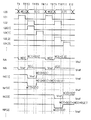
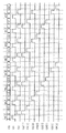
- a high potential is represented by “H” and a low potential is represented by “L”.
- the weight supplied to the pixel 10 [1] is “W [1]”
- the image data is “D [1]”
- the weight supplied to the pixel 10 [2] is “W [2]”
- the image data is “W [2]”.
- D [2] ".
- V ref for example, 0 V, a GND potential, or a specific reference potential can be used.
- the transistors 101 and 104 are turned on, and the potential of the wiring 126 is written to the node NA. Further, the potential of the node NA is written to the node NP [1]. This operation is a weight writing operation in both the circuit 11 and the pixel 10, and the potentials of the node NA and the node NP [1] become “W [1]”.
- the transistor 105 is turned on.
- the potential of the node NC becomes “W [1] + D [1] ′” and “(W [1] + D [1] ′) according to the capacitance ratio between the node NC [1] and the node NP [1].
- “” Is added to the node NP [1].
- This operation is an addition operation in the pixel 10, and the potential of the node NP [1] is "W [1] + (W [1] + D [1] ' -Vref )'".
- the potential of the node NP [1] is supplied to a display device, and display is performed.
- W [1] D [1]
- the capacity of the node NA is sufficiently smaller than the capacity of the node NB
- the capacity of the node NP [1] is sufficiently smaller than the capacity of the node NC [1].
- “W [1] + (W [1] + D [1] ′) ′” is a value close to “3D [1]”. Therefore, a data potential that is about three times the data potential output by the source driver can be supplied to the display device.
- the pixel 10 [2] By applying the same operation to the pixel 10 [2] from time T5 to time T8, the pixel 10 [2] performs display according to “W [2] + (W [2] + D [2] ′) ′”. It can be performed.
- V ref is written to the node NC.
- This operation is a writing operation of a weight in the pixel 10 and a reset operation for capacitive coupling, and the potential of the node NP [1] becomes “W [1] + D [1] ′”.
- W [1] D [1]
- the capacity of the node NA is sufficiently smaller than the capacity of the node NB
- the capacity of the node NP [1] is sufficiently smaller than the capacity of the node NC [1].
- “W [1] + D [1] ′ + (W [1] + D [1] ′) ′” is a value close to “4D [1]”. Therefore, a data potential that is about four times the data potential output from the source driver can be supplied to the display device.
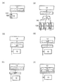
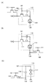
- FIGS. 7A to 7C illustrate an example of a structure which can be applied to the circuit block 110 and includes a light-emitting device as a display device.
- the structure illustrated in FIG. 7A includes a transistor 111, a capacitor 113, and a light-emitting device 114.
- One of a source and a drain of the transistor 111 is electrically connected to one electrode of the light-emitting device 114.
- One electrode of the light emitting device 114 is electrically connected to one electrode of the capacitor 113.
- the other electrode of capacitor 113 is electrically connected to the gate of transistor 111.
- the gate of the transistor 111 is electrically connected to the node NP.
- the other of the source and the drain of the transistor 111 is electrically connected to the wiring 128.
- the other electrode of the light-emitting device 114 is electrically connected to the wiring 129.
- the wirings 128 and 129 have a function of supplying power.
- the wiring 128 can supply high-potential power.
- the wiring 129 can supply a low-potential power supply.
- one electrode of the light-emitting device 114 is electrically connected to the wiring 128, and the other electrode of the light-emitting device 114 is electrically connected to the transistor 111 and the other of the source and the drain. May be.
- This configuration can be applied to another circuit block 110 including the light-emitting device 114.
- FIG. 7C illustrates a structure in which the transistor 112 is added to the structure of FIG.
- One of a source and a drain of the transistor 112 is electrically connected to one of a source and a drain of the transistor 111.
- the other of the source and the drain of the transistor 112 is electrically connected to one electrode of the light-emitting device 114.
- the gate of the transistor 112 is electrically connected to the wiring 127.
- the wiring 127 can function as a signal line for controlling conduction of the transistor 112.
- FIG. 7D illustrates a structure in which the transistor 115 is added to the structure of FIG.
- One of a source and a drain of the transistor 115 is electrically connected to one of a source and a drain of the transistor 111.
- the other of the source and the drain of the transistor 115 is electrically connected to the wiring 131.
- the gate of the transistor 115 is electrically connected to the wiring 132.
- the wiring 132 can function as a signal line for controlling conduction of the transistor 115.
- the wiring 131 can be electrically connected to a supply source of a specific potential such as a reference potential. By supplying a specific potential to one of the source and the drain of the transistor 111 from the wiring 131, writing of image data can be stabilized. Further, the light emission timing of the light emitting device 114 can be controlled.
- the wiring 131 can be connected to the circuit 120 and can have a function as a monitor line.
- the circuit 120 can have one or more of a supply source of the specific potential, a function of acquiring electric characteristics of the transistor 111, and a function of generating correction data.
- FIG. 8A to 8D illustrate an example of a structure which can be applied to the circuit block 110 and includes a liquid crystal device as a display device.
- FIG. 8A includes a capacitor 116 and a liquid crystal device 117.
- One electrode of the liquid crystal device 117 is electrically connected to one electrode of the capacitor 116.
- One electrode of capacitor 116 is electrically connected to node NP.
- the other electrode of the capacitor 116 is electrically connected to the wiring 133.
- the other electrode of the liquid crystal device 117 is electrically connected to the wiring 134.
- the wirings 133 and 134 have a function of supplying power.
- the wirings 133 and 134 can supply a reference potential such as GND or 0 V or an arbitrary potential.
- an OS transistor can be used as a transistor connected to the node NP. Since the OS transistor has extremely small leak current, display can be maintained for a relatively long time even if the capacitor 116 functioning as a storage capacitor is omitted. In addition to the structure of the transistor, it is effective to omit the capacitor 116 in a case where the display period can be shortened by high-speed operation, such as a field sequential drive. By eliminating the capacitor 116, the aperture ratio can be improved. Alternatively, the transmittance of the pixel can be improved.
- the operation of the liquid crystal device 117 starts when the potential of the node NP is determined to be equal to or higher than the operation threshold value of the liquid crystal device 117. Therefore, the display operation may start when the weight is written to the node NP, and the application may be limited. However, in the case of a transmissive liquid crystal display device, an unnecessary display operation is performed by using an operation such as turning off the backlight until the timing when the operation of adding the weight (W) and the data (D) is completed. However, the visual recognition can be suppressed.
- FIG. 8C illustrates a structure in which the transistor 118 is added to the structure of FIG.
- One of a source and a drain of the transistor 118 is electrically connected to one electrode of the capacitor 116.
- the other of the source and the drain of the transistor 118 is electrically connected to the node NP.
- the gate of the transistor 118 is electrically connected to the wiring 136.
- the wiring 136 can function as a signal line for controlling conduction of the transistor 118.
- the potential of the node NP is applied to the liquid crystal device 117 with the conduction of the transistor 118. Therefore, the operation of the liquid crystal device can be started at an arbitrary timing after the operation of adding the weight (W) and the data (D).
- the reset may be performed by, for example, supplying a reset potential to the wiring 125 and turning on the transistor 104 and the transistor 118 at the same time.
- FIG. 8D illustrates a structure in which a transistor 119 is added to the structure of FIG.
- One of a source and a drain of the transistor 119 is electrically connected to one electrode of the liquid crystal device 117.
- the other of the source and the drain of the transistor 119 is electrically connected to the wiring 131.
- the gate of the transistor 119 is electrically connected to the wiring 135.
- the wiring 135 can function as a signal line for controlling conduction of the transistor 119.
- the circuit 120 electrically connected to the wiring 131 is similar to that described with reference to FIG. 7D and may have a function of resetting the potential supplied to the capacitor 116 and the liquid crystal device 117. .
- FIGS. 9A to 9C are diagrams illustrating specific examples of wiring for supplying “V ref ” in the pixel 10 illustrated in FIG. 2 and the like.
- the wiring 128 can be used as a wiring for supplying “V ref ”. Since “V ref ” is preferably 0 V, GND, or a low potential, the wiring 128 also has a function of supplying at least one of those potentials. “V ref ” may be supplied to the wiring 128 at the timing of writing data to the node NP, and a high-potential power supply may be supplied at the timing of causing the light-emitting device 114 to emit light.
- a wiring 129 for supplying a low potential may be used as a wiring for supplying “V ref ”.
- a wiring 133 can be used as a wiring for supplying “V ref ”.
- the wiring 134 may be applied. Note that a dedicated common line for supplying “V ref ” may be provided regardless of the type of the display device.
- a transistor may be provided with a back gate.
- FIG. 10 illustrates a configuration in which the back gate is electrically connected to the front gate, which has an effect of increasing the on-state current.
- a structure in which the back gate is electrically connected to a wiring which can supply a constant potential may be employed. With such a structure, the threshold voltage of the transistor can be controlled.
- a back gate may be provided for a transistor included in the circuit block 110.
- FIG. 11 shows the configuration of the pixel (PIX) and the circuit 11 used in the simulation. Assuming that the number of pixels is four, the configuration (liquid crystal device and capacitor) shown in FIG. The simulation was performed on the voltage change of the node NP of each pixel in the operation of increasing the input voltage by about three times (hereinafter, operation 1) and the operation of boosting the input voltage by about four times (hereinafter, operation 2).
- the capacitance value of the capacitor C1 was 500 pF
- the capacitance value of the capacitor C2 was 5 pF
- the capacitance value of the capacitor Cs was 500 fF
- the capacitance value of the liquid crystal device Clc was 500 fF.
- the voltage applied to the gate of the transistor was +15 V for "H” and -15 V for "L”.
- the capacitance value of the capacitor C1 was 100 pF
- the capacitance value of the capacitor C2 was 10 pF
- the capacitance value of the capacitor Cs was 50 fF
- the capacitance value of the liquid crystal device Clc was 50 fF.
- the voltage applied to the gate of the transistor was +15 V for "H” and -20 V for "L".
- the wiring PL connecting the circuit 11 and the pixel PIX include the same number of resistors R1 corresponding to parasitic resistance and the same number of capacitors C3 corresponding to parasitic capacitance as the number of pixels.
- the parasitic capacitance (sum of C3) of the wiring PL was 0F and the resistance (sum of R1) of the wiring PL was 0 ⁇ .
- SPICE was used as the circuit simulation software.
- FIG. 12 is a timing chart used for the simulation of the operation 1.
- FIG. 13 is a timing chart used for the simulation of the operation 2.
- Weight (+ W), data (+ D) were +5 V
- weight (-W) were +5 V as parameters common to the operations 1 and 2.
- the potentials of V ref , VCOM, and TCOM were all set to 0V.
- the horizontal axis represents time (second), and the vertical axis represents the voltage (V) of the node NP.
- Each figure shows, on a time axis, a change in voltage at the node NP when a writing operation is performed on the pixels PIX [1] to PIX [4].
- This embodiment can be implemented in appropriate combination with the structures described in the other embodiments and the like.
- Embodiment 2 In this embodiment, a configuration example of a display device using a liquid crystal device and a configuration example of a display device using a light-emitting device will be described. Note that, in this embodiment, descriptions of the elements, operations, and functions of the display device described in Embodiment 1 are omitted.
- the display device described in this embodiment can use the addition circuit and the pixel described in Embodiment 1.
- a scanning line driver circuit described below corresponds to a gate driver
- a signal line driver circuit corresponds to a source driver.
- FIGS. 16A to 16C illustrate a structure of a display device to which one embodiment of the present invention can be applied.
- a sealant 4005 is provided so as to surround a display portion 215 provided over a first substrate 4001, and the display portion 215 is sealed with the sealant 4005 and the second substrate 4006. .
- the scan line driver circuit 221a, the signal line driver circuit 231a, the signal line driver circuit 232a, and the common line driver circuit 241a each include a plurality of integrated circuits 4042 provided over a printed board 4041.
- the integrated circuit 4042 is formed using a single crystal semiconductor or a polycrystalline semiconductor.
- the common line driver circuit 241a has a function of supplying a prescribed potential to the wirings 128, 129, 133, and 134 described in Embodiment 1.
- the integrated circuit 4042 included in the scan line driver circuit 221a and the common line driver circuit 241a has a function of supplying a selection signal to the display portion 215.
- the integrated circuit 4042 included in the signal line driver circuits 231a and 232a has a function of supplying image data to the display portion 215.
- the integrated circuit 4042 is mounted in a region on the first substrate 4001 which is different from a region surrounded by the sealant 4005.
- a method for connecting the integrated circuit 4042 and a wire bonding method, a COG (Chip On Glass) method, a TCP (Tape Carrier Package) method, a COF (Chip On Film) method, or the like can be used. it can.
- a COG Chip On Glass
- TCP Transmission Carrier Package
- COF Chip On Film
- FIG. 16B illustrates an example in which the integrated circuit 4042 included in the signal line driver circuit 231a and the signal line driver circuit 232a is mounted by a COG method. Further, part or the whole of the driver circuit can be formed over the same substrate as the display portion 215, whereby a system-on-panel can be formed.
- FIG. 16B illustrates an example in which the scan line driver circuit 221a and the common line driver circuit 241a are formed over the same substrate as the display portion 215.
- a sealant 4005 is provided so as to surround the display portion 215 provided over the first substrate 4001, the scan line driver circuit 221a, and the common line driver circuit 241a.
- a second substrate 4006 is provided over the display portion 215, the scan line driver circuit 221a, and the common line driver circuit 241a. Therefore, the display portion 215, the scan line driver circuit 221a, and the common line driver circuit 241a are sealed with the first substrate 4001, the sealant 4005, and the second substrate 4006.
- FIG. 16B illustrates an example in which the signal line driver circuit 231a and the signal line driver circuit 232a are separately formed and mounted on the first substrate 4001; however, this embodiment is not limited to this structure.
- the scan line driver circuit may be formed separately and mounted, or a part of the signal line driver circuit or a part of the scan line driver circuit may be formed separately and mounted.
- the signal line driver circuit 231a and the signal line driver circuit 232a may be formed over the same substrate as the display portion 215.
- the display device may include a panel in which the display device is sealed and a module in which an IC or the like including a controller is mounted on the panel.
- the display portion and the scan line driver circuit provided over the first substrate have a plurality of transistors.
- the transistor the transistor described in the above embodiment can be used.
- the structure of the transistor included in the peripheral driver circuit and the structure of the transistor included in the pixel circuit in the display portion may be the same or different.
- the transistors included in the peripheral driver circuit may all have the same structure, or may be a combination of two or more types of structures.
- all the transistors included in the pixel circuit may have the same structure or a combination of two or more types of structures.
- the input device 4200 can be provided over the second substrate 4006.
- the structure in which the input device 4200 is provided in the display device illustrated in FIGS. 16A to 16C can function as a touch panel.
- sensing element also referred to as a sensor element
- Various sensors that can detect the proximity or contact of a detection target such as a finger or a stylus can be applied as the detection element.
- a sensor system for example, various systems such as a capacitance system, a resistance film system, a surface acoustic wave system, an infrared system, an optical system, and a pressure-sensitive system can be used.
- a touch panel having a capacitance type sensing element will be described as an example.
- Examples of the capacitance type include a surface type capacitance type and a projection type capacitance type.
- the projection-type capacitance method includes a self-capacitance method, a mutual capacitance method, and the like. It is preferable to use the mutual capacitance method because simultaneous multipoint detection becomes possible.
- the touch panel of one embodiment of the present invention has a structure in which a separately manufactured display device and a sensing element are attached to each other, a structure in which an electrode or the like constituting a sensing element is provided on one or both of a substrate supporting a display device and a counter substrate, or the like.
- Various configurations can be applied.
- FIGS. 17A and 17B illustrate an example of a touch panel.
- FIG. 17A is a perspective view of the touch panel 4210.
- FIG. 17B is a schematic perspective view of the input device 4200. Note that only representative components are shown for clarity.
- the touch panel 4210 has a configuration in which a display device and a sensing element which are separately manufactured are attached to each other.
- the touch panel 4210 includes an input device 4200 and a display device, which are provided in an overlapping manner.
- the input device 4200 includes a substrate 4263, an electrode 4227, an electrode 4228, a plurality of wirings 4237, a plurality of wirings 4238, and a plurality of wirings 4239.
- the electrode 4227 can be electrically connected to the wiring 4237 or the wiring 4239.
- the electrode 4228 can be electrically connected to the wiring 4238.
- the FPC 4272b is electrically connected to each of the plurality of wirings 4237, 4238, and 4239.
- the FPC 4272b can be provided with an IC 4273b.
- a touch sensor may be provided between the first substrate 4001 and the second substrate 4006 of the display device.
- a touch sensor is provided between the first substrate 4001 and the second substrate 4006, an optical touch sensor using a photoelectric conversion element may be used in addition to a capacitive touch sensor.
- FIGS. 18A and 18B are cross-sectional views of a portion indicated by a chain line of N1-N2 in FIG. 16B.
- the display device illustrated in FIGS. 18A and 18B includes an electrode 4015, and the electrode 4015 is electrically connected to a terminal included in the FPC 4018 through an anisotropic conductive layer 4019.
- the electrode 4015 is electrically connected to the wiring 4014 in openings formed in the insulating layers 4112, 4111, and 4110.
- the electrode 4015 is formed using the same conductive layer as the first electrode layer 4030, and the wiring 4014 is formed using the same conductive layer as the source and drain electrodes of the transistor 4010 and the transistor 4011.
- the display portion 215 and the scan line driver circuit 221a provided over the first substrate 4001 have a plurality of transistors.
- a transistor 4010 included in the display portion 215 is included.
- a transistor 4011 included in the scanning line driver circuit 221a is included. Note that although a bottom-gate transistor is illustrated as the transistor 4010 and the transistor 4011 in FIGS. 18A and 18B, a top-gate transistor may be used.
- an insulating layer 4112 is provided over the transistor 4010 and the transistor 4011.
- a partition 4510 is formed over the insulating layer 4112.
- the transistor 4010 and the transistor 4011 are provided over the insulating layer 4102.
- the transistor 4010 and the transistor 4011 each include an electrode 4017 formed over the insulating layer 4111.
- the electrode 4017 can function as a back gate electrode.
- the display device illustrated in FIGS. 18A and 18B includes a capacitor 4020.
- the capacitor 4020 includes an electrode 4021 formed in the same step as the gate electrode of the transistor 4010, and an electrode formed in the same step as the source and drain electrodes. These electrodes overlap with an insulating layer 4103 interposed therebetween.
- the capacitance of a capacitor provided in a pixel portion of a display device is set so as to hold electric charge for a predetermined period in consideration of a leak current or the like of a transistor provided in the pixel portion.
- the capacity of the capacitor may be set in consideration of the off-state current or the like of a transistor electrically connected to the capacitor.
- FIG. 18A illustrates an example of a liquid crystal display device using a liquid crystal device as a display device.
- a liquid crystal device 4013 which is a display device includes a first electrode layer 4030, a second electrode layer 4031, and a liquid crystal layer 4008.
- an insulating layer 4032 and an insulating layer 4033 functioning as alignment films are provided so as to sandwich the liquid crystal layer 4008.
- the second electrode layer 4031 is provided on the second substrate 4006 side, and the first electrode layer 4030 and the second electrode layer 4031 overlap with each other with the liquid crystal layer 4008 interposed therebetween.
- liquid crystal devices to which various modes are applied can be used.
- a VA (Vertical Alignment) mode a TN (Twisted Nematic) mode, an IPS (In-Plane-Switching) mode, an ASM (Axially Symmetrical Aligned Microelectronic Cellular Cruiser Electronics Co., Ltd. ) Mode, AFLC (Anti Ferro Electric Liquid Crystal) mode, ECB (Electrically Controlled Birefringence) mode, VA-IPS mode, guest host mode, or the like can be used.
- a normally black liquid crystal display device such as a transmissive liquid crystal display device employing a vertical alignment (VA) mode may be applied to the liquid crystal display device described in this embodiment.
- VA vertical alignment
- an MVA (Multi-Domain Vertical Alignment) mode a PVA (Patterned Vertical Alignment) mode, an ASV (Advanced Super View) mode, or the like can be used.
- a liquid crystal device is an element that controls transmission or non-transmission of light by an optical modulation action of liquid crystal.
- the optical modulation action of the liquid crystal is controlled by an electric field (including a horizontal electric field, a vertical electric field, or an oblique electric field) applied to the liquid crystal.
- an electric field including a horizontal electric field, a vertical electric field, or an oblique electric field
- a thermotropic liquid crystal a low molecular liquid crystal
- a polymer liquid crystal a polymer dispersed liquid crystal (PDLC: Polymer Dispersed Liquid Crystal)
- ferroelectric liquid crystal an antiferroelectric liquid crystal, or the like
- These liquid crystal materials show a cholesteric phase, a smectic phase, a cubic phase, a chiral nematic phase, an isotropic phase, or the like depending on conditions.
- FIG. 18A illustrates an example of a liquid crystal display device including a vertical electric field liquid crystal device; however, a liquid crystal display device including a horizontal electric field liquid crystal device can be applied to one embodiment of the present invention.
- a liquid crystal exhibiting a blue phase without using an alignment film may be used.
- the blue phase is one of the liquid crystal phases, and is a phase that appears when the temperature of the cholesteric liquid crystal is raised immediately before the transition from the cholesteric phase to the isotropic phase. Since the blue phase appears only in a narrow temperature range, a liquid crystal composition in which a chiral agent of 5% by weight or more is mixed is used for the liquid crystal layer 4008 in order to improve the temperature range.
- a liquid crystal composition containing a liquid crystal exhibiting a blue phase and a chiral agent has a short response speed and exhibits optical isotropy. Further, a liquid crystal composition containing a liquid crystal exhibiting a blue phase and a chiral agent does not require an alignment treatment and has a small viewing angle dependence. Further, since it is not necessary to provide an alignment film, rubbing treatment is not required, so that electrostatic breakdown caused by the rubbing treatment can be prevented, and defects or breakage of a liquid crystal display device during a manufacturing process can be reduced. .
- the spacer 4035 is a columnar spacer obtained by selectively etching an insulating layer, and is provided for controlling a distance (cell gap) between the first electrode layer 4030 and the second electrode layer 4031. ing. Note that a spherical spacer may be used.
- a black matrix light-shielding layer
- a coloring layer color filter
- an optical member optical substrate
- circularly polarized light from a polarizing substrate and a retardation substrate may be used.
- a backlight, a sidelight, or the like may be used as a light source.
- a micro LED or the like may be used as the backlight and the sidelight.
- a light-blocking layer 4132, a coloring layer 4131, and an insulating layer 4133 are provided between the substrate 4006 and the second electrode layer 4031.
- Examples of a material that can be used as the light-shielding layer include carbon black, titanium black, a metal, a metal oxide, and a composite oxide containing a solid solution of a plurality of metal oxides.
- the light shielding layer may be a film containing a resin material or a thin film of an inorganic material such as a metal.
- a stacked film of a film containing a material used for the coloring layer can be used for the light-blocking layer.
- a stacked structure of a film containing a material used for a colored layer transmitting light of a certain color and a film containing a material used for a colored layer transmitting light of another color can be employed. It is preferable to use a common material for the coloring layer and the light-shielding layer, because the device can be shared and the process can be simplified.
- Examples of a material that can be used for the coloring layer include a metal material, a resin material, and a resin material containing a pigment or a dye.
- the formation of the light-shielding layer and the colored layer may be performed in the same manner as the formation of each layer described above. For example, it may be performed by an inkjet method or the like.
- the display device illustrated in FIGS. 18A and 18B includes an insulating layer 4111 and an insulating layer 4104.
- an insulating layer 4111 and the insulating layer 4104 an insulating layer which does not easily transmit an impurity element is used. By sandwiching the semiconductor layer of the transistor between the insulating layer 4111 and the insulating layer 4104, entry of impurities from the outside can be prevented.
- a light-emitting device can be used as a display device included in the display device.
- an EL element utilizing electroluminescence can be used.
- An EL element includes a layer containing a light-emitting compound (also referred to as an “EL layer”) between a pair of electrodes. When a potential difference larger than the threshold voltage of the EL element is generated between the pair of electrodes, holes are injected into the EL layer from the anode side and electrons are injected from the cathode side. The injected electrons and holes are recombined in the EL layer, and the light-emitting substance contained in the EL layer emits light.
- EL elements are distinguished depending on whether the light-emitting material is an organic compound or an inorganic compound. Generally, the former is called an organic EL element and the latter is called an inorganic EL element.
- an organic EL element In an organic EL element, electrons are injected from one electrode and holes are injected from the other electrode into the EL layer by applying a voltage. Then, by recombination of the carriers (electrons and holes), the light-emitting organic compound forms an excited state, and the organic compound emits light when the excited state returns to the ground state. Due to such a mechanism, such a light emitting device is called a current excitation type light emitting device.
- the EL layer is formed using a substance having a high hole-injection property, a substance having a high hole-transport property, a hole-blocking material, a substance having a high electron-transport property, a substance having a high electron-injection property, or a bipolar substance. (A substance having a high electron-transport property and a high hole-transport property) or the like.
- the EL layer can be formed by a method such as an evaporation method (including a vacuum evaporation method), a transfer method, a printing method, an inkjet method, and a coating method.
- a method such as an evaporation method (including a vacuum evaporation method), a transfer method, a printing method, an inkjet method, and a coating method.
- Inorganic EL elements are classified according to their element structures into a dispersion-type inorganic EL element and a thin-film inorganic EL element.
- the dispersion-type inorganic EL element has a light-emitting layer in which particles of a light-emitting material are dispersed in a binder.
- the light-emission mechanism is donor-acceptor recombination light emission using a donor level and an acceptor level.
- the thin-film inorganic EL device has a structure in which a light emitting layer is sandwiched between dielectric layers and further sandwiched between electrodes, and the light emission mechanism is localized light emission using inner-shell electron transition of metal ions. Note that here, an organic EL element will be described as a light emitting device.
- the light emitting device only needs to be transparent at least one of the pair of electrodes in order to extract light emission. Then, a transistor and a light emitting device are formed over the substrate, and a top emission (top emission) structure for extracting light emission from a surface opposite to the substrate, a bottom emission (bottom emission) structure for extracting light emission from a surface on the substrate side, and the like. There is a light emitting device having a dual emission (dual emission) structure in which light is emitted from both surfaces, and any light emitting device having an emission structure can be applied.
- FIG. 18B illustrates an example of a light-emitting display device using a light-emitting device as a display device (also referred to as an “EL display device”).
- a light-emitting device 4513 which is a display device is electrically connected to the transistor 4010 provided in the display portion 215.
- the structure of the light-emitting device 4513 is a stacked structure of the first electrode layer 4030, the light-emitting layer 4511, and the second electrode layer 4031; however, the structure is not limited to this.
- the structure of the light-emitting device 4513 can be changed as appropriate depending on the direction of light extracted from the light-emitting device 4513 and the like.
- the partition 4510 is formed using an organic insulating material or an inorganic insulating material.
- an opening be formed on the first electrode layer 4030 using a photosensitive resin material, and that the side surface of the opening be formed as an inclined surface having a continuous curvature.
- the light-emitting layer 4511 may be formed of a single layer or a structure in which a plurality of layers are stacked.
- the light-emitting color of the light-emitting device 4513 can be white, red, green, blue, cyan, magenta, yellow, or the like depending on the material of the light-emitting layer 4511.
- a method for achieving color display there are a method in which a light-emitting device 4513 emitting white light is combined with a coloring layer, and a method in which a light-emitting device 4513 having a different emission color is provided for each pixel.
- the former method is more productive than the latter method.
- the latter method since the light emitting layer 4511 needs to be separately formed for each pixel, the productivity is lower than the former method.
- the latter method can provide a luminescent color with higher color purity than the former method.
- the color purity can be further increased.
- the light-emitting layer 4511 may include an inorganic compound such as a quantum dot.
- an inorganic compound such as a quantum dot.
- a quantum dot for a light emitting layer, it can be made to function as a light emitting material.
- a protective layer may be formed over the second electrode layer 4031 and the partition 4510 so that oxygen, hydrogen, moisture, carbon dioxide, and the like do not enter the light-emitting device 4513.
- the protective layer silicon nitride, silicon nitride oxide, aluminum oxide, aluminum nitride, aluminum oxynitride, aluminum nitride oxide, DLC (Diamond Like Carbon), or the like can be formed.
- a filler 4514 is provided and sealed.
- a protective film a laminated film, an ultraviolet curable resin film, or the like
- a cover material that has high airtightness and low degassing so as not to be exposed to the outside air.
- an ultraviolet curable resin or a thermosetting resin in addition to an inert gas such as nitrogen or argon, an ultraviolet curable resin or a thermosetting resin can be used.
- PVC polyvinyl chloride
- acrylic resin acrylic resin
- polyimide polyimide
- epoxy resin epoxy resin
- silicone resin polyimide
- EVA ethylene vinyl acetate
- a desiccant may be included in the filler 4514.
- a glass material such as a glass frit, or a resin material such as a two-component resin that cures at room temperature, a photocurable resin, or a thermosetting resin can be used. Further, a desiccant may be included in the sealant 4005.
- an optical film such as a polarizing plate, a circularly polarizing plate (including an elliptically polarizing plate), a retardation plate ( ⁇ / 4 plate, ⁇ / 2 plate), and a color filter may be provided on the emission surface of the light emitting device. It may be provided as appropriate. Further, an antireflection film may be provided on a polarizing plate or a circularly polarizing plate. For example, anti-glare treatment can be performed in which reflected light is diffused by unevenness on the surface to reduce glare.
- the light-emitting device has a microcavity structure
- light with high color purity can be extracted.
- reflection can be reduced and visibility of a displayed image can be improved.
- a first electrode layer and a second electrode layer (also referred to as a pixel electrode layer, a common electrode layer, a counter electrode layer, and the like) for applying a voltage to a display device, a direction of light to be extracted, a place where the electrode layer is provided, and Light transmission or reflection may be selected depending on the pattern structure of the electrode layer.
- the first electrode layer 4030 and the second electrode layer 4031 are formed using indium oxide containing tungsten oxide, indium zinc oxide containing tungsten oxide, indium oxide containing titanium oxide, indium tin oxide, and indium containing titanium oxide.
- a light-transmitting conductive material such as tin oxide, indium zinc oxide, or indium tin oxide to which silicon oxide is added can be used.
- the first electrode layer 4030 and the second electrode layer 4031 are made of tungsten (W), molybdenum (Mo), zirconium (Zr), hafnium (Hf), vanadium (V), niobium (Nb), and tantalum (Ta).
- Metal such as chromium (Cr), cobalt (Co), nickel (Ni), titanium (Ti), platinum (Pt), aluminum (Al), copper (Cu), silver (Ag), or an alloy thereof It can be formed using one or more kinds of metal nitride.
- the first electrode layer 4030 and the second electrode layer 4031 can be formed using a conductive composition including a conductive high molecule (also referred to as a conductive polymer).
- a conductive high molecule also referred to as a conductive polymer.
- a so-called ⁇ -electron conjugated conductive high molecule can be used.
- polyaniline or a derivative thereof, polypyrrole or a derivative thereof, polythiophene or a derivative thereof, and a copolymer of two or more of aniline, pyrrole, and thiophene or a derivative thereof, and the like can be given.
- a protection circuit for protecting a driver circuit is preferably provided.
- the protection circuit is preferably formed using a non-linear element.
- FIG. 19 illustrates an example in which the stack structure is applied to the liquid crystal display device illustrated in FIG. 18A; however, the liquid crystal display device illustrated in FIG. 18B may be applied to an EL display device.
- a conductive film having a high light-transmitting property with respect to visible light for an electrode or a wiring by using a conductive film having a high light-transmitting property with respect to visible light for an electrode or a wiring, light transmittance in a pixel can be increased, and an aperture ratio can be substantially improved. it can.
- the semiconductor layer when an OS transistor is used, the semiconductor layer also has a light-transmitting property; thus, the aperture ratio can be further increased.
- a display device may be configured by combining a liquid crystal display device and a light emitting device.
- the light emitting device is arranged on the opposite side of the display surface or at the end of the display surface.
- the light-emitting device has a function of supplying light to a display device.
- the light-emitting device can also be called a backlight.
- the light-emitting device can include a plate-shaped or sheet-shaped light guide portion (also referred to as a light guide plate) and a plurality of light-emitting devices that emit light of different colors.
- a plate-shaped or sheet-shaped light guide portion also referred to as a light guide plate
- a plurality of light-emitting devices that emit light of different colors.
- the light guide has a mechanism for changing the optical path (also referred to as a light extraction mechanism), whereby the light emitting device can uniformly irradiate the pixel portion of the display panel with light.
- a structure in which a light emitting device is arranged immediately below a pixel without providing a light guide portion may be employed.
- the light emitting device has light emitting devices of three colors of red (R), green (G), and blue (B). Further, a white (W) light emitting device may be provided. It is preferable to use a light emitting diode (LED: Light Emitting Diode) as these light emitting devices.
- LED Light Emitting Diode
- the light emitting device has a full width at half maximum (FWHM: Full Width at at Half Maximum) of 50 nm or less, preferably 40 nm or less, more preferably 30 nm or less, and still more preferably 20 nm or less. It is preferably a light emitting device.
- FWHM Full Width at at Half Maximum
- the full width at half maximum of the emission spectrum is preferably as small as possible, but may be, for example, 1 nm or more. Thereby, when performing color display, a vivid display with high color reproducibility can be performed.
- the red light-emitting device it is preferable to use an element whose emission spectrum has a peak wavelength in a range from 625 nm to 650 nm.
- the green light-emitting device it is preferable to use an element having a peak wavelength of an emission spectrum in a range of 515 nm to 540 nm.
- the blue light-emitting device it is preferable to use an element whose peak wavelength of the emission spectrum is in the range of 445 nm to 470 nm.
- the display device blinks the light emitting devices of three colors sequentially, drives the pixels in synchronization with the light emitting devices, and performs color display based on the successive additive color mixing method.
- the driving method can also be referred to as field sequential driving.
- a vivid color image can be displayed.
- a smooth moving image can be displayed.
- one pixel does not need to be formed of a plurality of sub-pixels of different colors, and the effective reflection area (also referred to as an effective display area or an aperture ratio) of one pixel can be increased. Display can be performed. Further, since it is not necessary to provide a color filter for the pixel, the transmittance of the pixel can be improved, and a brighter display can be performed. Further, the manufacturing process can be simplified, and manufacturing cost can be reduced.
- 20A and 20B are examples of schematic cross-sectional views of a display device capable of performing field sequential driving.
- a backlight unit capable of emitting light of each color of RGB is provided on the substrate 4001 side of the display device.
- a color filter is unnecessary.
- a backlight unit 4340a illustrated in FIG. 20A has a structure in which a plurality of light-emitting devices 4342 are provided directly below a pixel with a diffusion plate 4352 interposed therebetween.
- the diffusion plate 4352 has a function of diffusing light emitted from the light-emitting device 4342 to the substrate 4001 side and uniforming luminance in a display portion surface.
- a polarizing plate may be provided between the light emitting device 4342 and the diffusion plate 4352 as needed.
- the diffusion plate 4352 may not be provided if unnecessary. Further, the light-blocking layer 4132 may be omitted.
- the backlight unit 4340a can include a large number of light-emitting devices 4342, bright display can be performed. Further, a light guide plate is unnecessary, and there is an advantage that the light efficiency of the light emitting device 4342 is hardly impaired. Note that the light emitting device 4342 may be provided with a light diffusion lens 4344 as needed.
- a backlight unit 4340b illustrated in FIG. 20B has a structure in which a light guide plate 4341 is provided directly below a pixel with a diffusion plate 4352 therebetween. At an end of the light guide plate 4341, a plurality of light emitting devices 4342 are provided.
- the light guide plate 4341 has a concavo-convex shape on the side opposite to the diffusion plate 4352, and can scatter the guided light in the concavo-convex shape and emit the light toward the diffusion plate 4352.
- the light emitting device 4342 can be fixed to the printed board 4347. Note that in FIG. 20B, the light emitting devices 4342 of each color of RGB are illustrated so as to overlap with each other, but the light emitting devices 4342 of each color of RGB can be arranged in the depth direction.
- a reflective layer 4348 that reflects visible light may be provided on a side surface opposite to the light emitting device 4342.
- the backlight unit 4340b can be reduced in cost and thickness.
- a light scattering type liquid crystal device may be used as the liquid crystal device.
- the light-scattering liquid crystal device an element having a composite material of liquid crystal and a polymer is preferably used.
- a polymer dispersed liquid crystal device can be used.
- a polymer network type liquid crystal (PNLC (Polymer Network Liquid Crystal)) element may be used.
- the light scattering type liquid crystal device has a structure in which a liquid crystal portion is provided in a three-dimensional network structure of a resin portion sandwiched between a pair of electrodes.
- a material used for the liquid crystal portion for example, a nematic liquid crystal can be used.
- a photocurable resin can be used as the resin portion.
- a monofunctional monomer such as acrylate and methacrylate
- a polyfunctional monomer such as diacrylate, triacrylate, dimethacrylate, and trimethacrylate, or a polymerizable compound obtained by mixing these can be used.
- the light scattering type liquid crystal device performs display by transmitting or scattering light by utilizing anisotropy of a refractive index of a liquid crystal material. Further, the resin portion may also have anisotropy of the refractive index.
- the liquid crystal molecules are arranged in a certain direction according to the voltage applied to the light scattering type liquid crystal device, a direction in which the difference in the refractive index between the liquid crystal part and the resin part becomes small occurs, and light incident along the direction is generated in the liquid crystal part. Transmit without scattering. Therefore, the light scattering type liquid crystal device is visually recognized in a transparent state from the direction.
- the light scattering type liquid crystal device is in an opaque state regardless of the viewing direction.
- FIG. 21A illustrates a structure in which the liquid crystal device 4013 of the display device in FIG. 20A is replaced with a light-scattering liquid crystal device 4016.
- the light-scattering liquid crystal device 4016 includes a composite layer 4009 having a liquid crystal portion and a resin portion, and electrode layers 4030 and 4031. Elements related to field sequential driving are the same as those in FIG. 20A. However, when the light scattering type liquid crystal device 4016 is used, an alignment film and a polarizing plate are not required.
- the spacer 4035 is illustrated in a spherical shape, it may be in a column shape.
- FIG. 21B illustrates a structure in which the liquid crystal device 4013 of the display device in FIG. 20B is replaced with a light-scattering liquid crystal device 4016.
- the light-scattering liquid crystal device 4016 operate in a mode in which light is transmitted when no voltage is applied and light is scattered when a voltage is applied.
- a transparent display device can be provided in a normal state (a state in which display is not performed). In this case, color display can be performed when an operation of scattering light is performed.
- FIGS. 21B Modifications of the display device illustrated in FIG. 21B are illustrated in FIGS. Note that in FIGS. 22A to 22E, for clarity, some components in FIG. 21B are used and other components are omitted.
- FIG. 22A illustrates a structure in which the substrate 4001 has a function as a light guide plate.
- An uneven surface may be provided on the outer surface of the substrate 4001. In this configuration, it is not necessary to separately provide a light guide plate, so that manufacturing cost can be reduced. Further, since light is not attenuated by the light guide plate, light emitted from the light emitting device 4342 can be efficiently used.
- FIG. 22B illustrates a structure in which light enters from near the end of the composite layer 4009.
- Light can be emitted from the light-scattering type liquid crystal device to the outside by utilizing total reflection at the interface between the composite layer 4009 and the substrate 4006 and at the interface between the composite layer 4009 and the substrate 4001.
- a material having a higher refractive index than the substrates 4001 and 4006 is used.
- the light-emitting device 4342 may be provided not only on one side of the display device but also on two opposing sides as shown in FIG. Further, it may be provided on three or four sides. By providing the light-emitting device 4342 on a plurality of sides, light attenuation can be compensated, and a display device having a large area can be supported.
- FIG. 22D illustrates a structure in which light emitted from the light-emitting device 4342 is guided to the display device through the mirror 4345.
- FIG. 22E illustrates a structure in which a layer 4003 and a layer 4004 are stacked over a composite layer 4009.
- One of the layers 4003 and 4004 is a support such as a glass substrate, and the other can be formed using an inorganic film, a coating film or a film of an organic resin, or the like.
- a material having a higher refractive index than the layer 4004 is used for the resin portion of the composite layer 4009.
- a material having a higher refractive index than the layer 4003 is used.
- a first interface is formed between the composite layer 4009 and the layer 4004, and a second interface is formed between the layer 4004 and the layer 4003.
- FIG. 21B and FIGS. 22A to 22E can be combined with each other.
- This embodiment can be implemented in appropriate combination with the structures described in the other embodiments and the like.
- the display device of one embodiment of the present invention can be manufactured using various types of transistors such as a bottom-gate transistor and a top-gate transistor. Therefore, the material of the semiconductor layer and the transistor structure to be used can be easily replaced according to the existing manufacturing line.
- FIG. 23A1 is a cross-sectional view in the channel length direction of a channel-protection transistor 810 which is a kind of bottom-gate transistor.
- the transistor 810 is formed over a substrate 771.
- the transistor 810 includes an electrode 746 over a substrate 771 with an insulating layer 772 interposed therebetween.
- a semiconductor layer 742 is provided over the electrode 746 with an insulating layer 726 interposed therebetween.
- the electrode 746 can function as a gate electrode.
- the insulating layer 726 can function as a gate insulating layer.
- an insulating layer 741 is provided over a channel formation region of the semiconductor layer 742. Further, an electrode 744a and an electrode 744b are provided over the insulating layer 726 in contact with part of the semiconductor layer 742.
- the electrode 744a can function as one of a source electrode and a drain electrode.
- the electrode 744b can function as the other of the source electrode and the drain electrode. Part of the electrode 744a and part of the electrode 744b are formed over the insulating layer 741.
- the insulating layer 741 can function as a channel protective layer. Providing the insulating layer 741 over the channel formation region can prevent the semiconductor layer 742 from being exposed when the electrodes 744a and 744b are formed. Therefore, the channel formation region of the semiconductor layer 742 can be prevented from being etched when the electrodes 744a and 744b are formed. According to one embodiment of the present invention, a transistor with favorable electric characteristics can be realized.
- the transistor 810 includes the insulating layer 728 over the electrode 744a, the electrode 744b, and the insulating layer 741, and the insulating layer 729 over the insulating layer 728.
- an oxide semiconductor used for the semiconductor layer 742
- a material which can remove oxygen from part of the semiconductor layer 742 and generate oxygen vacancies is used for at least a portion of the electrode 744a and the electrode 744b which is in contact with the semiconductor layer 742.
- the carrier concentration increases, the region becomes n-type, and the region becomes an n-type region (n + layer). Therefore, the region can function as a source region or a drain region.
- tungsten, titanium, or the like can be given as an example of a material capable of removing oxygen from the semiconductor layer 742 and causing oxygen vacancies.
- the contact resistance between the electrodes 744a and 744b and the semiconductor layer 742 can be reduced.
- favorable electric characteristics of the transistor such as a field-effect mobility and a threshold voltage, can be obtained.
- a layer which functions as an n-type semiconductor or a p-type semiconductor is preferably provided between the semiconductor layer 742 and the electrode 744a and between the semiconductor layer 742 and the electrode 744b.
- a layer functioning as an n-type semiconductor or a p-type semiconductor can function as a source region or a drain region of a transistor.
- the insulating layer 729 is preferably formed using a material having a function of preventing or reducing diffusion of impurities from the outside to the transistor. Note that the insulating layer 729 can be omitted as necessary.
- a transistor 811 illustrated in FIG. 23A2 has an electrode 723 which can function as a back gate electrode over an insulating layer 729, which is different from the transistor 810.
- the electrode 723 can be formed using a material and a method similar to those of the electrode 746.
- a back gate electrode is formed using a conductive layer, and is arranged so that a channel formation region of a semiconductor layer is sandwiched between the gate electrode and the back gate electrode.
- the back gate electrode can function similarly to the gate electrode.
- the potential of the back gate electrode may be the same potential as the gate electrode, a ground potential (GND potential), or an arbitrary potential.
- the threshold voltage of the transistor can be changed by independently changing the potential of the back gate electrode without interlocking with the gate electrode.
- both the electrode 746 and the electrode 723 can function as gate electrodes. Therefore, each of the insulating layers 726, 728, and 729 can function as a gate insulating layer. Note that the electrode 723 may be provided between the insulating layer 728 and the insulating layer 729.
- the other is referred to as a “back gate electrode”.
- the electrode 746 when the electrode 723 is referred to as a “gate electrode”, the electrode 746 is referred to as a “back gate electrode”.
- the transistor 811 can be considered as a kind of top-gate transistor.
- one of the electrode 746 and the electrode 723 may be referred to as a “first gate electrode”, and the other may be referred to as a “second gate electrode”.
- the electrode 746 and the electrode 723 With the electrode 746 and the electrode 723 with the semiconductor layer 742 interposed therebetween, and further by setting the electrode 746 and the electrode 723 to the same potential, a region where carriers flow in the semiconductor layer 742 becomes larger in the thickness direction. The amount of carrier movement increases. As a result, the on-state current of the transistor 811 increases and the field-effect mobility increases.
- the transistor 811 is a transistor having a large on-state current with respect to an occupied area. That is, the area occupied by the transistor 811 can be reduced with respect to the required on-state current. According to one embodiment of the present invention, the area occupied by a transistor can be reduced. Thus, according to one embodiment of the present invention, a highly integrated semiconductor device can be realized.
- the gate electrode and the back gate electrode are formed using a conductive layer, the gate electrode and the back gate electrode have a function of preventing an electric field generated outside the transistor from acting on a semiconductor layer in which a channel is formed (particularly, a function of shielding an electric field against static electricity or the like). . Note that by forming the back gate electrode larger than the semiconductor layer and covering the semiconductor layer with the back gate electrode, the electric field shielding function can be improved.
- the back gate electrode is formed using a conductive film having a light-blocking property
- light can be prevented from entering the semiconductor layer from the back gate electrode side. Accordingly, light deterioration of the semiconductor layer can be prevented, and deterioration of electrical characteristics such as a shift in threshold voltage of the transistor can be prevented.
- a highly reliable transistor can be realized. Further, a highly reliable semiconductor device can be realized.
- FIG. 23B1 is a cross-sectional view in the channel length direction of a channel protection transistor 820 having a different structure from FIG.
- the transistor 820 has substantially the same structure as the transistor 810, except that an insulating layer 741 covers an end portion of the semiconductor layer 742.
- the semiconductor layer 742 and the electrode 744a are electrically connected to each other at an opening portion formed by selectively removing a part of the insulating layer 741 which overlaps with the semiconductor layer 742.
- the semiconductor layer 742 and the electrode 744b are electrically connected.
- a region of the insulating layer 741 which overlaps with the channel formation region can function as a channel protective layer.
- a transistor 821 illustrated in FIG. 23B2 has an electrode 723 which can function as a back gate electrode over an insulating layer 729, which is different from the transistor 820.
- the provision of the insulating layer 741 can prevent the semiconductor layer 742 from being exposed when the electrodes 744a and 744b are formed. Therefore, the thickness of the semiconductor layer 742 can be prevented from being reduced when the electrodes 744a and 744b are formed.
- the distance between the electrode 744a and the electrode 746 and the distance between the electrode 744b and the electrode 746 are longer in the transistor 820 and the transistor 821 than in the transistor 810 and the transistor 811. Therefore, parasitic capacitance generated between the electrode 744a and the electrode 746 can be reduced. Further, parasitic capacitance generated between the electrode 744b and the electrode 746 can be reduced. According to one embodiment of the present invention, a transistor with favorable electric characteristics can be realized.
- FIG. 23C1 is a cross-sectional view in the channel length direction of a channel-etched transistor 825 which is one of bottom-gate transistors.
- the electrodes 744a and 744b are formed without using the insulating layer 729. Therefore, part of the semiconductor layer 742 exposed when the electrodes 744a and 744b are formed may be etched. On the other hand, since the insulating layer 729 is not provided, the productivity of the transistor can be increased.
- a transistor 826 illustrated in FIG. 23C2 has an electrode 723 which can function as a back gate electrode over an insulating layer 729, which is different from the transistor 820.
- FIGS. 24A1 to 24C2 are cross-sectional views of the transistors 810, 811, 820, 821, 825, and 826 in the channel width direction, respectively.
- the gate electrode and the back gate electrode are connected, and the gate electrode and the back gate electrode have the same potential. Further, the semiconductor layer 742 is sandwiched between a gate electrode and a back gate electrode.
- each of the gate electrode and the back gate electrode in the channel width direction is longer than the length of the semiconductor layer 742 in the channel width direction.
- the entire semiconductor layer 742 in the channel width direction is formed by insulating layers 726, 741, 728, and 729. It is configured to be covered with a gate electrode and a back gate electrode sandwiched therebetween.
- the semiconductor layer 742 included in the transistor can be electrically surrounded by electric fields of the gate electrode and the back gate electrode.
- a device structure of a transistor, such as the transistor 821 and the transistor 826, which electrically surrounds the semiconductor layer 742 in which a channel formation region is formed by an electric field of a gate electrode and a back gate electrode is referred to as a Surrounded channel (S-channel) structure. Can be.
- the S-channel structure an electric field for inducing a channel by one or both of the gate electrode and the back gate electrode can be effectively applied to the semiconductor layer 742, so that the current driving capability of the transistor is improved. And high on-current characteristics can be obtained. Further, since the on-state current can be increased, the transistor can be miniaturized. In addition, with the S-channel structure, the mechanical strength of the transistor can be increased.
- the transistor 842 illustrated in FIG. 25A1 is one of top-gate transistors.
- the electrodes 744a and 744b are electrically connected to the semiconductor layer 742 in openings formed in the insulating layers 728 and 729.
- the transistor 842 has a region in which the insulating layer 726 extends beyond the end of the electrode 746.
- the impurity concentration of a region of the semiconductor layer 742 where impurities are introduced through the insulating layer 726 is lower than that of a region where impurities are introduced without passing through the insulating layer 726. Therefore, in the semiconductor layer 742, an LDD (Lightly Doped Drain) region is formed in a region which does not overlap with the electrode 746.
- LDD Lightly Doped Drain
- a transistor 843 illustrated in FIG. 25A2 is different from the transistor 842 in having an electrode 723.
- the transistor 843 has an electrode 723 formed over a substrate 771.
- the electrode 723 has a region overlapping with the semiconductor layer 742 with the insulating layer 772 interposed therebetween.
- the electrode 723 can function as a back gate electrode.
- all of the insulating layer 726 in a region which does not overlap with the electrode 746 may be removed.
- the insulating layer 726 may be left as in the transistor 846 illustrated in FIG. 25C1 and the transistor 847 illustrated in FIG. 25C2.
- an impurity region can be formed in the semiconductor layer 742 in a self-aligned manner by introducing an impurity into the semiconductor layer 742 using the electrode 746 as a mask after the electrode 746 is formed.
- a transistor with favorable electric characteristics can be realized.
- a highly integrated semiconductor device can be realized.
- 26A1 to 26C2 are cross-sectional views in the channel width direction of the transistors 842, 843, 844, 845, 846, and 847, respectively.
- Each of the transistor 843, the transistor 845, and the transistor 847 has the S-channel structure described above. Note that this embodiment is not limited to this example.
- the transistor 843, the transistor 845, and the transistor 847 need not have an S-channel structure.
- This embodiment can be implemented in appropriate combination with the structures described in the other embodiments and the like.
- a display device As electronic devices that can use the display device according to one embodiment of the present invention, a display device, a personal computer, an image storage device or an image reproducing device provided with a recording medium, a mobile phone, a game machine including a mobile device, and a mobile data terminal , E-book terminals, video cameras, cameras such as digital still cameras, goggle-type displays (head-mounted displays), navigation systems, sound reproducers (car audio, digital audio players, etc.), copiers, facsimile machines, printers, multifunction printers , An automatic teller machine (ATM), a vending machine, and the like.
- FIG. 27 illustrates specific examples of these electronic devices.
- FIG. 27A illustrates a digital camera, which includes a housing 961, a shutter button 962, a microphone 963, a speaker 967, a display portion 965, operation keys 966, a zoom lever 968, a lens 969, and the like.
- a digital camera which includes a housing 961, a shutter button 962, a microphone 963, a speaker 967, a display portion 965, operation keys 966, a zoom lever 968, a lens 969, and the like.
- FIG. 27B illustrates a digital signage including a large display portion 922.
- a large display portion 922 is attached to a side surface of a pillar 921.
- the display device of one embodiment of the present invention for the display portion 922 high-quality display can be performed.
- FIG. 27C illustrates a mobile phone, which includes a housing 951, a display portion 952, operation buttons 953, an external connection port 954, a speaker 955, a microphone 956, a camera 957, and the like.
- the mobile phone includes a touch sensor in the display portion 952. All operations such as making a call and inputting characters can be performed by touching the display portion 952 with a finger, a stylus, or the like. Further, the housing 951 and the display portion 952 have flexibility and can be used by being bent as illustrated. With the use of the display device of one embodiment of the present invention for the display portion 952, various images can be displayed.
- FIG. 27D illustrates a video camera, which includes a first housing 901, a second housing 902, a display portion 903, operation keys 904, a lens 905, a connection portion 906, a speaker 907, and the like.
- the operation keys 904 and the lens 905 are provided on the first housing 901, and the display unit 903 is provided on the second housing 902.
- the display portion 903 With the use of the display device of one embodiment of the present invention for the display portion 903, various images can be displayed.
- FIG. 27E illustrates a television, which includes a housing 971, a display portion 973, operation keys 974, a speaker 975, a communication connection terminal 976, an optical sensor 977, and the like.
- the display portion 973 is provided with a touch sensor and can perform an input operation. With the use of the display device of one embodiment of the present invention for the display portion 973, various images can be displayed.
- FIG. 27F illustrates a portable data terminal, which includes a housing 911, a display portion 912, a speaker 913, a camera 919, and the like. Information can be input and output using the touch panel function of the display portion 912. With the use of the display device of one embodiment of the present invention for the display portion 912, various images can be displayed.
- This embodiment can be implemented in appropriate combination with the structures described in the other embodiments and the like.
Landscapes
- Engineering & Computer Science (AREA)
- Physics & Mathematics (AREA)
- General Physics & Mathematics (AREA)
- Theoretical Computer Science (AREA)
- Computer Hardware Design (AREA)
- Crystallography & Structural Chemistry (AREA)
- Chemical & Material Sciences (AREA)
- Nonlinear Science (AREA)
- Optics & Photonics (AREA)
- Mathematical Physics (AREA)
- Microelectronics & Electronic Packaging (AREA)
- Thin Film Transistor (AREA)
- Control Of Indicators Other Than Cathode Ray Tubes (AREA)
- Electroluminescent Light Sources (AREA)
- Liquid Crystal (AREA)
- Liquid Crystal Display Device Control (AREA)
- Devices For Indicating Variable Information By Combining Individual Elements (AREA)
- Control Of El Displays (AREA)
Priority Applications (6)
| Application Number | Priority Date | Filing Date | Title |
|---|---|---|---|
| JP2020528539A JP7374896B2 (ja) | 2018-07-05 | 2019-06-25 | 表示装置および電子機器 |
| KR1020217000374A KR102799415B1 (ko) | 2018-07-05 | 2019-06-25 | 표시 장치 및 전자 기기 |
| CN202211409019.2A CN115527508A (zh) | 2018-07-05 | 2019-06-25 | 显示装置及电子设备 |
| US17/256,819 US11521569B2 (en) | 2018-07-05 | 2019-06-25 | Display apparatus and electronic device |
| CN201980042063.4A CN112313736B (zh) | 2018-07-05 | 2019-06-25 | 显示装置及电子设备 |
| US17/992,024 US11715435B2 (en) | 2018-07-05 | 2022-11-22 | Display apparatus and electronic device |
Applications Claiming Priority (2)
| Application Number | Priority Date | Filing Date | Title |
|---|---|---|---|
| JP2018128173 | 2018-07-05 | ||
| JP2018-128173 | 2018-07-05 |
Related Child Applications (2)
| Application Number | Title | Priority Date | Filing Date |
|---|---|---|---|
| US17/256,819 A-371-Of-International US11521569B2 (en) | 2018-07-05 | 2019-06-25 | Display apparatus and electronic device |
| US17/992,024 Continuation US11715435B2 (en) | 2018-07-05 | 2022-11-22 | Display apparatus and electronic device |
Publications (1)
| Publication Number | Publication Date |
|---|---|
| WO2020008299A1 true WO2020008299A1 (ja) | 2020-01-09 |
Family
ID=69060751
Family Applications (1)
| Application Number | Title | Priority Date | Filing Date |
|---|---|---|---|
| PCT/IB2019/055325 Ceased WO2020008299A1 (ja) | 2018-07-05 | 2019-06-25 | 表示装置および電子機器 |
Country Status (5)
| Country | Link |
|---|---|
| US (2) | US11521569B2 (enExample) |
| JP (1) | JP7374896B2 (enExample) |
| KR (1) | KR102799415B1 (enExample) |
| CN (2) | CN112313736B (enExample) |
| WO (1) | WO2020008299A1 (enExample) |
Cited By (1)
| Publication number | Priority date | Publication date | Assignee | Title |
|---|---|---|---|---|
| CN114241913A (zh) * | 2021-12-21 | 2022-03-25 | 湖北长江新型显示产业创新中心有限公司 | 可弯折显示模组及显示装置 |
Families Citing this family (3)
| Publication number | Priority date | Publication date | Assignee | Title |
|---|---|---|---|---|
| TWI731788B (zh) * | 2020-09-11 | 2021-06-21 | 宏碁股份有限公司 | 行動裝置 |
| CN115472626A (zh) * | 2021-05-24 | 2022-12-13 | 京东方科技集团股份有限公司 | 显示基板及其制作方法、显示装置 |
| JP2024169345A (ja) * | 2023-05-23 | 2024-12-05 | ブリルニクス シンガポール プライベート リミテッド | 固体撮像装置、固体撮像装置の製造方法、および電子機器 |
Citations (6)
| Publication number | Priority date | Publication date | Assignee | Title |
|---|---|---|---|---|
| JP2011039269A (ja) * | 2009-08-11 | 2011-02-24 | Seiko Epson Corp | 発光装置、電子機器および発光装置の駆動方法 |
| US20120249509A1 (en) * | 2011-03-29 | 2012-10-04 | Samsung Electronics Co., Ltd. | Pixel circuit and method of operating the same |
| US20140111491A1 (en) * | 2012-10-24 | 2014-04-24 | Lg Display Co., Ltd. | Liquid Crystal Display Device and Method for Driving the Same |
| JP2014215495A (ja) * | 2013-04-26 | 2014-11-17 | 株式会社Jvcケンウッド | 液晶表示装置及び液晶表示装置の検査方法 |
| KR20140143989A (ko) * | 2013-06-10 | 2014-12-18 | 엘지디스플레이 주식회사 | 액정표시장치 및 그 구동방법과 제조방법 |
| US20160055817A1 (en) * | 2014-08-19 | 2016-02-25 | Au Optronics Corp. | Panel driving circuit, booster circuit for liquid crystal pixel data and driving method thereof |
Family Cites Families (26)
| Publication number | Priority date | Publication date | Assignee | Title |
|---|---|---|---|---|
| WO2002035507A1 (en) | 2000-10-27 | 2002-05-02 | Matsushita Electric Industrial Co., Ltd. | Display |
| JP2002333870A (ja) | 2000-10-31 | 2002-11-22 | Matsushita Electric Ind Co Ltd | 液晶表示装置、el表示装置及びその駆動方法、並びに副画素の表示パターン評価方法 |
| JP4493359B2 (ja) * | 2004-02-05 | 2010-06-30 | 東北パイオニア株式会社 | 自発光表示モジュールおよびその駆動方法 |
| JP5064747B2 (ja) | 2005-09-29 | 2012-10-31 | 株式会社半導体エネルギー研究所 | 半導体装置、電気泳動表示装置、表示モジュール、電子機器、及び半導体装置の作製方法 |
| EP1998373A3 (en) | 2005-09-29 | 2012-10-31 | Semiconductor Energy Laboratory Co, Ltd. | Semiconductor device having oxide semiconductor layer and manufacturing method thereof |
| JP5078246B2 (ja) | 2005-09-29 | 2012-11-21 | 株式会社半導体エネルギー研究所 | 半導体装置、及び半導体装置の作製方法 |
| TWI344128B (en) | 2006-09-05 | 2011-06-21 | Ind Tech Res Inst | Charge pump pixel driving circuit |
| JP4300491B2 (ja) * | 2007-03-13 | 2009-07-22 | ソニー株式会社 | ディスプレイ装置 |
| TWI366176B (en) | 2007-07-19 | 2012-06-11 | Ind Tech Res Inst | Charge pump pixel driving circuit |
| JP2009109600A (ja) | 2007-10-29 | 2009-05-21 | Hitachi Displays Ltd | 液晶表示装置 |
| KR101752348B1 (ko) | 2009-10-30 | 2017-06-29 | 가부시키가이샤 한도오따이 에네루기 켄큐쇼 | 반도체 장치 |
| JP5779660B2 (ja) * | 2011-11-24 | 2015-09-16 | 株式会社Joled | 表示装置及びその制御方法 |
| JP6535441B2 (ja) * | 2014-08-06 | 2019-06-26 | セイコーエプソン株式会社 | 電気光学装置、電子機器、及び電気光学装置の駆動方法 |
| JP6832634B2 (ja) | 2015-05-29 | 2021-02-24 | 株式会社半導体エネルギー研究所 | 半導体装置 |
| US9773787B2 (en) * | 2015-11-03 | 2017-09-26 | Semiconductor Energy Laboratory Co., Ltd. | Semiconductor device, memory device, electronic device, or method for driving the semiconductor device |
| WO2017115208A1 (en) * | 2015-12-28 | 2017-07-06 | Semiconductor Energy Laboratory Co., Ltd. | Device, television system, and electronic device |
| WO2017135244A1 (ja) * | 2016-02-01 | 2017-08-10 | 株式会社ニコン | 撮像素子の製造方法、撮像素子、および撮像装置 |
| CN107437401A (zh) | 2016-05-26 | 2017-12-05 | 鸿富锦精密工业(深圳)有限公司 | 像素驱动电路以及具有像素驱动电路的显示装置 |
| US10586495B2 (en) * | 2016-07-22 | 2020-03-10 | Semiconductor Energy Laboratory Co., Ltd. | Display device and electronic device |
| DE112017003898B4 (de) * | 2016-08-03 | 2024-07-18 | Semiconductor Energy Laboratory Co., Ltd. | Abbildungsvorrichtungen und Bildsensor |
| CN115359757B (zh) | 2017-11-09 | 2025-05-27 | 株式会社半导体能源研究所 | 显示装置及其工作方法以及电子设备 |
| JP7291631B2 (ja) | 2017-12-21 | 2023-06-15 | 株式会社半導体エネルギー研究所 | 表示装置 |
| US11360363B2 (en) | 2018-01-19 | 2022-06-14 | Semiconductor Energy Laboratory Co., Ltd. | Display apparatus having pixels connected to first and second wirings set to different potentials |
| KR20230164225A (ko) | 2018-02-01 | 2023-12-01 | 가부시키가이샤 한도오따이 에네루기 켄큐쇼 | 표시 장치 및 전자 기기 |
| JP7235731B2 (ja) | 2018-04-26 | 2023-03-08 | 株式会社半導体エネルギー研究所 | 表示装置および電子機器 |
| US11430404B2 (en) * | 2018-05-25 | 2022-08-30 | Semiconductor Energy Laboratory Co., Ltd. | Display device including pixel and electronic device |
-
2019
- 2019-06-25 KR KR1020217000374A patent/KR102799415B1/ko active Active
- 2019-06-25 CN CN201980042063.4A patent/CN112313736B/zh not_active Expired - Fee Related
- 2019-06-25 JP JP2020528539A patent/JP7374896B2/ja active Active
- 2019-06-25 CN CN202211409019.2A patent/CN115527508A/zh active Pending
- 2019-06-25 WO PCT/IB2019/055325 patent/WO2020008299A1/ja not_active Ceased
- 2019-06-25 US US17/256,819 patent/US11521569B2/en active Active
-
2022
- 2022-11-22 US US17/992,024 patent/US11715435B2/en active Active
Patent Citations (6)
| Publication number | Priority date | Publication date | Assignee | Title |
|---|---|---|---|---|
| JP2011039269A (ja) * | 2009-08-11 | 2011-02-24 | Seiko Epson Corp | 発光装置、電子機器および発光装置の駆動方法 |
| US20120249509A1 (en) * | 2011-03-29 | 2012-10-04 | Samsung Electronics Co., Ltd. | Pixel circuit and method of operating the same |
| US20140111491A1 (en) * | 2012-10-24 | 2014-04-24 | Lg Display Co., Ltd. | Liquid Crystal Display Device and Method for Driving the Same |
| JP2014215495A (ja) * | 2013-04-26 | 2014-11-17 | 株式会社Jvcケンウッド | 液晶表示装置及び液晶表示装置の検査方法 |
| KR20140143989A (ko) * | 2013-06-10 | 2014-12-18 | 엘지디스플레이 주식회사 | 액정표시장치 및 그 구동방법과 제조방법 |
| US20160055817A1 (en) * | 2014-08-19 | 2016-02-25 | Au Optronics Corp. | Panel driving circuit, booster circuit for liquid crystal pixel data and driving method thereof |
Cited By (2)
| Publication number | Priority date | Publication date | Assignee | Title |
|---|---|---|---|---|
| CN114241913A (zh) * | 2021-12-21 | 2022-03-25 | 湖北长江新型显示产业创新中心有限公司 | 可弯折显示模组及显示装置 |
| CN114241913B (zh) * | 2021-12-21 | 2023-06-16 | 湖北长江新型显示产业创新中心有限公司 | 可弯折显示模组及显示装置 |
Also Published As
| Publication number | Publication date |
|---|---|
| KR20210027358A (ko) | 2021-03-10 |
| US20210366422A1 (en) | 2021-11-25 |
| CN112313736A (zh) | 2021-02-02 |
| CN115527508A (zh) | 2022-12-27 |
| KR102799415B1 (ko) | 2025-04-22 |
| US20230089084A1 (en) | 2023-03-23 |
| US11715435B2 (en) | 2023-08-01 |
| US11521569B2 (en) | 2022-12-06 |
| JPWO2020008299A1 (ja) | 2021-08-19 |
| CN112313736B (zh) | 2022-12-02 |
| JP7374896B2 (ja) | 2023-11-07 |
Similar Documents
| Publication | Publication Date | Title |
|---|---|---|
| JP7488927B2 (ja) | 表示装置 | |
| US11715435B2 (en) | Display apparatus and electronic device | |
| JP7689595B2 (ja) | 表示装置 | |
| JP7487111B2 (ja) | 表示装置および電子機器 | |
| JP7412360B2 (ja) | 表示装置および電子機器 | |
| US12488767B2 (en) | Display apparatus and electronic device | |
| JP7315572B2 (ja) | 表示装置および電子機器 |
Legal Events
| Date | Code | Title | Description |
|---|---|---|---|
| 121 | Ep: the epo has been informed by wipo that ep was designated in this application |
Ref document number: 19830593 Country of ref document: EP Kind code of ref document: A1 |
|
| ENP | Entry into the national phase |
Ref document number: 2020528539 Country of ref document: JP Kind code of ref document: A |
|
| NENP | Non-entry into the national phase |
Ref country code: DE |
|
| 122 | Ep: pct application non-entry in european phase |
Ref document number: 19830593 Country of ref document: EP Kind code of ref document: A1 |