WO2020008294A1 - 金属酸窒化物膜の作製方法 - Google Patents
金属酸窒化物膜の作製方法 Download PDFInfo
- Publication number
- WO2020008294A1 WO2020008294A1 PCT/IB2019/055287 IB2019055287W WO2020008294A1 WO 2020008294 A1 WO2020008294 A1 WO 2020008294A1 IB 2019055287 W IB2019055287 W IB 2019055287W WO 2020008294 A1 WO2020008294 A1 WO 2020008294A1
- Authority
- WO
- WIPO (PCT)
- Prior art keywords
- metal oxynitride
- oxynitride film
- plane
- sample
- substrate
- Prior art date
- Legal status (The legal status is an assumption and is not a legal conclusion. Google has not performed a legal analysis and makes no representation as to the accuracy of the status listed.)
- Ceased
Links
Images





Classifications
-
- C—CHEMISTRY; METALLURGY
- C30—CRYSTAL GROWTH
- C30B—SINGLE-CRYSTAL GROWTH; UNIDIRECTIONAL SOLIDIFICATION OF EUTECTIC MATERIAL OR UNIDIRECTIONAL DEMIXING OF EUTECTOID MATERIAL; REFINING BY ZONE-MELTING OF MATERIAL; PRODUCTION OF A HOMOGENEOUS POLYCRYSTALLINE MATERIAL WITH DEFINED STRUCTURE; SINGLE CRYSTALS OR HOMOGENEOUS POLYCRYSTALLINE MATERIAL WITH DEFINED STRUCTURE; AFTER-TREATMENT OF SINGLE CRYSTALS OR A HOMOGENEOUS POLYCRYSTALLINE MATERIAL WITH DEFINED STRUCTURE; APPARATUS THEREFOR
- C30B25/00—Single-crystal growth by chemical reaction of reactive gases, e.g. chemical vapour-deposition growth
- C30B25/02—Epitaxial-layer growth
- C30B25/06—Epitaxial-layer growth by reactive sputtering
-
- H—ELECTRICITY
- H10—SEMICONDUCTOR DEVICES; ELECTRIC SOLID-STATE DEVICES NOT OTHERWISE PROVIDED FOR
- H10P—GENERIC PROCESSES OR APPARATUS FOR THE MANUFACTURE OR TREATMENT OF DEVICES COVERED BY CLASS H10
- H10P14/00—Formation of materials, e.g. in the shape of layers or pillars
- H10P14/20—Formation of materials, e.g. in the shape of layers or pillars of semiconductor materials
- H10P14/29—Formation of materials, e.g. in the shape of layers or pillars of semiconductor materials characterised by the substrates
- H10P14/2901—Materials
- H10P14/2921—Materials being crystalline insulating materials
-
- H—ELECTRICITY
- H10—SEMICONDUCTOR DEVICES; ELECTRIC SOLID-STATE DEVICES NOT OTHERWISE PROVIDED FOR
- H10P—GENERIC PROCESSES OR APPARATUS FOR THE MANUFACTURE OR TREATMENT OF DEVICES COVERED BY CLASS H10
- H10P14/00—Formation of materials, e.g. in the shape of layers or pillars
- H10P14/60—Formation of materials, e.g. in the shape of layers or pillars of insulating materials
- H10P14/63—Formation of materials, e.g. in the shape of layers or pillars of insulating materials characterised by the formation processes
- H10P14/6326—Deposition processes
- H10P14/6328—Deposition from the gas or vapour phase
- H10P14/6329—Deposition from the gas or vapour phase using physical ablation of a target, e.g. physical vapour deposition or pulsed laser deposition
-
- C—CHEMISTRY; METALLURGY
- C23—COATING METALLIC MATERIAL; COATING MATERIAL WITH METALLIC MATERIAL; CHEMICAL SURFACE TREATMENT; DIFFUSION TREATMENT OF METALLIC MATERIAL; COATING BY VACUUM EVAPORATION, BY SPUTTERING, BY ION IMPLANTATION OR BY CHEMICAL VAPOUR DEPOSITION, IN GENERAL; INHIBITING CORROSION OF METALLIC MATERIAL OR INCRUSTATION IN GENERAL
- C23C—COATING METALLIC MATERIAL; COATING MATERIAL WITH METALLIC MATERIAL; SURFACE TREATMENT OF METALLIC MATERIAL BY DIFFUSION INTO THE SURFACE, BY CHEMICAL CONVERSION OR SUBSTITUTION; COATING BY VACUUM EVAPORATION, BY SPUTTERING, BY ION IMPLANTATION OR BY CHEMICAL VAPOUR DEPOSITION, IN GENERAL
- C23C14/00—Coating by vacuum evaporation, by sputtering or by ion implantation of the coating forming material
- C23C14/0021—Reactive sputtering or evaporation
- C23C14/0036—Reactive sputtering
-
- C—CHEMISTRY; METALLURGY
- C23—COATING METALLIC MATERIAL; COATING MATERIAL WITH METALLIC MATERIAL; CHEMICAL SURFACE TREATMENT; DIFFUSION TREATMENT OF METALLIC MATERIAL; COATING BY VACUUM EVAPORATION, BY SPUTTERING, BY ION IMPLANTATION OR BY CHEMICAL VAPOUR DEPOSITION, IN GENERAL; INHIBITING CORROSION OF METALLIC MATERIAL OR INCRUSTATION IN GENERAL
- C23C—COATING METALLIC MATERIAL; COATING MATERIAL WITH METALLIC MATERIAL; SURFACE TREATMENT OF METALLIC MATERIAL BY DIFFUSION INTO THE SURFACE, BY CHEMICAL CONVERSION OR SUBSTITUTION; COATING BY VACUUM EVAPORATION, BY SPUTTERING, BY ION IMPLANTATION OR BY CHEMICAL VAPOUR DEPOSITION, IN GENERAL
- C23C14/00—Coating by vacuum evaporation, by sputtering or by ion implantation of the coating forming material
- C23C14/06—Coating by vacuum evaporation, by sputtering or by ion implantation of the coating forming material characterised by the coating material
- C23C14/0676—Oxynitrides
-
- C—CHEMISTRY; METALLURGY
- C23—COATING METALLIC MATERIAL; COATING MATERIAL WITH METALLIC MATERIAL; CHEMICAL SURFACE TREATMENT; DIFFUSION TREATMENT OF METALLIC MATERIAL; COATING BY VACUUM EVAPORATION, BY SPUTTERING, BY ION IMPLANTATION OR BY CHEMICAL VAPOUR DEPOSITION, IN GENERAL; INHIBITING CORROSION OF METALLIC MATERIAL OR INCRUSTATION IN GENERAL
- C23C—COATING METALLIC MATERIAL; COATING MATERIAL WITH METALLIC MATERIAL; SURFACE TREATMENT OF METALLIC MATERIAL BY DIFFUSION INTO THE SURFACE, BY CHEMICAL CONVERSION OR SUBSTITUTION; COATING BY VACUUM EVAPORATION, BY SPUTTERING, BY ION IMPLANTATION OR BY CHEMICAL VAPOUR DEPOSITION, IN GENERAL
- C23C14/00—Coating by vacuum evaporation, by sputtering or by ion implantation of the coating forming material
- C23C14/06—Coating by vacuum evaporation, by sputtering or by ion implantation of the coating forming material characterised by the coating material
- C23C14/08—Oxides
-
- C—CHEMISTRY; METALLURGY
- C23—COATING METALLIC MATERIAL; COATING MATERIAL WITH METALLIC MATERIAL; CHEMICAL SURFACE TREATMENT; DIFFUSION TREATMENT OF METALLIC MATERIAL; COATING BY VACUUM EVAPORATION, BY SPUTTERING, BY ION IMPLANTATION OR BY CHEMICAL VAPOUR DEPOSITION, IN GENERAL; INHIBITING CORROSION OF METALLIC MATERIAL OR INCRUSTATION IN GENERAL
- C23C—COATING METALLIC MATERIAL; COATING MATERIAL WITH METALLIC MATERIAL; SURFACE TREATMENT OF METALLIC MATERIAL BY DIFFUSION INTO THE SURFACE, BY CHEMICAL CONVERSION OR SUBSTITUTION; COATING BY VACUUM EVAPORATION, BY SPUTTERING, BY ION IMPLANTATION OR BY CHEMICAL VAPOUR DEPOSITION, IN GENERAL
- C23C14/00—Coating by vacuum evaporation, by sputtering or by ion implantation of the coating forming material
- C23C14/22—Coating by vacuum evaporation, by sputtering or by ion implantation of the coating forming material characterised by the process of coating
- C23C14/34—Sputtering
-
- C—CHEMISTRY; METALLURGY
- C30—CRYSTAL GROWTH
- C30B—SINGLE-CRYSTAL GROWTH; UNIDIRECTIONAL SOLIDIFICATION OF EUTECTIC MATERIAL OR UNIDIRECTIONAL DEMIXING OF EUTECTOID MATERIAL; REFINING BY ZONE-MELTING OF MATERIAL; PRODUCTION OF A HOMOGENEOUS POLYCRYSTALLINE MATERIAL WITH DEFINED STRUCTURE; SINGLE CRYSTALS OR HOMOGENEOUS POLYCRYSTALLINE MATERIAL WITH DEFINED STRUCTURE; AFTER-TREATMENT OF SINGLE CRYSTALS OR A HOMOGENEOUS POLYCRYSTALLINE MATERIAL WITH DEFINED STRUCTURE; APPARATUS THEREFOR
- C30B25/00—Single-crystal growth by chemical reaction of reactive gases, e.g. chemical vapour-deposition growth
- C30B25/02—Epitaxial-layer growth
- C30B25/18—Epitaxial-layer growth characterised by the substrate
-
- C—CHEMISTRY; METALLURGY
- C30—CRYSTAL GROWTH
- C30B—SINGLE-CRYSTAL GROWTH; UNIDIRECTIONAL SOLIDIFICATION OF EUTECTIC MATERIAL OR UNIDIRECTIONAL DEMIXING OF EUTECTOID MATERIAL; REFINING BY ZONE-MELTING OF MATERIAL; PRODUCTION OF A HOMOGENEOUS POLYCRYSTALLINE MATERIAL WITH DEFINED STRUCTURE; SINGLE CRYSTALS OR HOMOGENEOUS POLYCRYSTALLINE MATERIAL WITH DEFINED STRUCTURE; AFTER-TREATMENT OF SINGLE CRYSTALS OR A HOMOGENEOUS POLYCRYSTALLINE MATERIAL WITH DEFINED STRUCTURE; APPARATUS THEREFOR
- C30B29/00—Single crystals or homogeneous polycrystalline material with defined structure characterised by the material or by their shape
- C30B29/10—Inorganic compounds or compositions
- C30B29/38—Nitrides
-
- H—ELECTRICITY
- H10—SEMICONDUCTOR DEVICES; ELECTRIC SOLID-STATE DEVICES NOT OTHERWISE PROVIDED FOR
- H10D—INORGANIC ELECTRIC SEMICONDUCTOR DEVICES
- H10D30/00—Field-effect transistors [FET]
- H10D30/60—Insulated-gate field-effect transistors [IGFET]
- H10D30/67—Thin-film transistors [TFT]
-
- H—ELECTRICITY
- H10—SEMICONDUCTOR DEVICES; ELECTRIC SOLID-STATE DEVICES NOT OTHERWISE PROVIDED FOR
- H10D—INORGANIC ELECTRIC SEMICONDUCTOR DEVICES
- H10D30/00—Field-effect transistors [FET]
- H10D30/60—Insulated-gate field-effect transistors [IGFET]
- H10D30/67—Thin-film transistors [TFT]
- H10D30/674—Thin-film transistors [TFT] characterised by the active materials
- H10D30/6755—Oxide semiconductors, e.g. zinc oxide, copper aluminium oxide or cadmium stannate
-
- H—ELECTRICITY
- H10—SEMICONDUCTOR DEVICES; ELECTRIC SOLID-STATE DEVICES NOT OTHERWISE PROVIDED FOR
- H10H—INORGANIC LIGHT-EMITTING SEMICONDUCTOR DEVICES HAVING POTENTIAL BARRIERS
- H10H20/00—Individual inorganic light-emitting semiconductor devices having potential barriers, e.g. light-emitting diodes [LED]
- H10H20/01—Manufacture or treatment
- H10H20/032—Manufacture or treatment of electrodes
-
- H—ELECTRICITY
- H10—SEMICONDUCTOR DEVICES; ELECTRIC SOLID-STATE DEVICES NOT OTHERWISE PROVIDED FOR
- H10H—INORGANIC LIGHT-EMITTING SEMICONDUCTOR DEVICES HAVING POTENTIAL BARRIERS
- H10H20/00—Individual inorganic light-emitting semiconductor devices having potential barriers, e.g. light-emitting diodes [LED]
- H10H20/80—Constructional details
- H10H20/81—Bodies
- H10H20/817—Bodies characterised by the crystal structures or orientations, e.g. polycrystalline, amorphous or porous
-
- H—ELECTRICITY
- H10—SEMICONDUCTOR DEVICES; ELECTRIC SOLID-STATE DEVICES NOT OTHERWISE PROVIDED FOR
- H10P—GENERIC PROCESSES OR APPARATUS FOR THE MANUFACTURE OR TREATMENT OF DEVICES COVERED BY CLASS H10
- H10P14/00—Formation of materials, e.g. in the shape of layers or pillars
- H10P14/20—Formation of materials, e.g. in the shape of layers or pillars of semiconductor materials
- H10P14/22—Formation of materials, e.g. in the shape of layers or pillars of semiconductor materials using physical deposition, e.g. vacuum deposition or sputtering
-
- H—ELECTRICITY
- H10—SEMICONDUCTOR DEVICES; ELECTRIC SOLID-STATE DEVICES NOT OTHERWISE PROVIDED FOR
- H10P—GENERIC PROCESSES OR APPARATUS FOR THE MANUFACTURE OR TREATMENT OF DEVICES COVERED BY CLASS H10
- H10P14/00—Formation of materials, e.g. in the shape of layers or pillars
- H10P14/20—Formation of materials, e.g. in the shape of layers or pillars of semiconductor materials
- H10P14/29—Formation of materials, e.g. in the shape of layers or pillars of semiconductor materials characterised by the substrates
- H10P14/2926—Crystal orientations
-
- H—ELECTRICITY
- H10—SEMICONDUCTOR DEVICES; ELECTRIC SOLID-STATE DEVICES NOT OTHERWISE PROVIDED FOR
- H10P—GENERIC PROCESSES OR APPARATUS FOR THE MANUFACTURE OR TREATMENT OF DEVICES COVERED BY CLASS H10
- H10P14/00—Formation of materials, e.g. in the shape of layers or pillars
- H10P14/20—Formation of materials, e.g. in the shape of layers or pillars of semiconductor materials
- H10P14/34—Deposited materials, e.g. layers
- H10P14/3402—Deposited materials, e.g. layers characterised by the chemical composition
- H10P14/3424—Deposited materials, e.g. layers characterised by the chemical composition being Group IIB-VIA materials
- H10P14/3426—Oxides
-
- H—ELECTRICITY
- H10—SEMICONDUCTOR DEVICES; ELECTRIC SOLID-STATE DEVICES NOT OTHERWISE PROVIDED FOR
- H10P—GENERIC PROCESSES OR APPARATUS FOR THE MANUFACTURE OR TREATMENT OF DEVICES COVERED BY CLASS H10
- H10P14/00—Formation of materials, e.g. in the shape of layers or pillars
- H10P14/20—Formation of materials, e.g. in the shape of layers or pillars of semiconductor materials
- H10P14/34—Deposited materials, e.g. layers
- H10P14/3402—Deposited materials, e.g. layers characterised by the chemical composition
- H10P14/3434—Deposited materials, e.g. layers characterised by the chemical composition being oxide semiconductor materials
-
- H—ELECTRICITY
- H10—SEMICONDUCTOR DEVICES; ELECTRIC SOLID-STATE DEVICES NOT OTHERWISE PROVIDED FOR
- H10P—GENERIC PROCESSES OR APPARATUS FOR THE MANUFACTURE OR TREATMENT OF DEVICES COVERED BY CLASS H10
- H10P14/00—Formation of materials, e.g. in the shape of layers or pillars
- H10P14/60—Formation of materials, e.g. in the shape of layers or pillars of insulating materials
- H10P14/63—Formation of materials, e.g. in the shape of layers or pillars of insulating materials characterised by the formation processes
- H10P14/6326—Deposition processes
- H10P14/6349—Deposition of epitaxial materials
-
- H—ELECTRICITY
- H10—SEMICONDUCTOR DEVICES; ELECTRIC SOLID-STATE DEVICES NOT OTHERWISE PROVIDED FOR
- H10P—GENERIC PROCESSES OR APPARATUS FOR THE MANUFACTURE OR TREATMENT OF DEVICES COVERED BY CLASS H10
- H10P14/00—Formation of materials, e.g. in the shape of layers or pillars
- H10P14/60—Formation of materials, e.g. in the shape of layers or pillars of insulating materials
- H10P14/69—Inorganic materials
- H10P14/692—Inorganic materials composed of oxides, glassy oxides or oxide-based glasses
- H10P14/6938—Inorganic materials composed of oxides, glassy oxides or oxide-based glasses the material containing at least one metal element, e.g. metal oxides, metal oxynitrides or metal oxycarbides
Definitions
- One embodiment of the present invention relates to a metal oxynitride film and a method for manufacturing the metal oxynitride film.
- One embodiment of the present invention relates to a light-emitting element, a lighting device, a display device, an electronic device, and a semiconductor device using the metal oxynitride film.
- a semiconductor device in this specification and the like refers to any device that can function by utilizing semiconductor characteristics.
- a semiconductor device such as a transistor, a semiconductor circuit, an arithmetic device, and a memory device are one embodiment of a semiconductor device.
- a display device (a liquid crystal display device, a light-emitting display device, or the like), a projection device, a lighting device, an electro-optical device, a power storage device, a storage device, a semiconductor circuit, an imaging device, an electronic device, or the like sometimes includes a semiconductor device.
- One embodiment of the present invention is not limited to the above technical field.
- One embodiment of the invention disclosed in this specification and the like relates to an object, a method, or a manufacturing method.
- One embodiment of the present invention relates to a process, a machine, a manufacturer, or a composition (composition of matter).
- Patent Literature 1 discloses a semiconductor material having a metal oxynitride containing indium, gallium, and zinc.
- Patent Document 2 discloses a method of forming a single-crystal InGaO 3 (ZnO) 5 thin film by a reactive solid-phase epitaxial method.
- the state of metal oxynitride disclosed in Patent Document 1 is an amorphous state in which bonds between atoms are disordered. Since the amorphous metal oxynitride has voids or low-density regions, the stability of the metal oxynitride is low. Therefore, a metal oxynitride used for a semiconductor device or the like preferably has high crystallinity. In particular, the metal oxynitride is preferably in-plane orientation.
- a process of heating a substrate to 1000 ° C. or higher is performed before forming an InGaO 3 (ZnO) 5 thin film.
- a high temperature treatment such as performing a heat diffusion treatment at a temperature of 1300 ° C. or more is required.
- a high temperature refers to, for example, a temperature of 700 ° C. or higher
- a low temperature refers to, for example, a temperature of 600 ° C. or lower.
- One embodiment of the present invention is a method for manufacturing a metal oxynitride film which is epitaxially grown by a sputtering method with introduction of a gas containing nitrogen gas over a single crystal substrate,
- the object target contains zinc
- the substrate on which the metal oxynitride film is being formed is 80 ° C. or more and 400 ° C. or less
- the flow rate of the nitrogen gas is 50% or more and 100% or less of the total gas flow rate.
- Another embodiment of the present invention is a metal oxynitride in which a gas containing nitrogen gas is introduced over a single crystal substrate and an in-plane oriented film is formed by a sputtering method with the use of an oxide target.
- the oxide target contains zinc
- the substrate during formation of the metal oxynitride film has a temperature of 80 ° C. or more and 400 ° C. or less
- the flow rate of the nitrogen gas is 50% or more and 100% or less.
- the oxide target preferably contains at least one of indium and gallium.
- the substrate is preferably a yttria-stabilized zirconia (YSZ) substrate, and the plane orientation of the substrate is preferably (111).
- the substrate is preferably an A-plane sapphire substrate, and the plane orientation of the substrate is preferably (110).
- the crystal structure of the metal oxynitride film is preferably a wurtzite structure.
- the pole measurement is performed on the metal oxynitride film
- the pole measurement is performed by ⁇ scan of the crystal (101) plane of the metal oxynitride film. , It is preferable that a diffraction peak showing six-fold symmetry is observed.
- a first spot and a second spot are observed in a wide area reciprocal lattice space map of the metal oxynitride film, and the peak of the first spot has an angle 2 ⁇ is 30 ° or more and 35 ° or less, and angle ⁇ is near 0 °, the half-value width of the first spot is less than 2 °, and the peak of the second spot has an angle 2 ⁇ of 33 ° or more.
- the angle ° is not less than 37 ° and not more than 61 ° and not more than 65 °
- the half width of the second spot is less than 2 °.
- a method for forming a metal oxynitride film by epitaxial growth at a low temperature can be provided. Further, according to one embodiment of the present invention, a method can be provided in which a metal oxynitride film is formed by epitaxial growth without performing high-temperature treatment before and after the formation of the metal oxynitride film. According to one embodiment of the present invention, a semiconductor device or the like using a metal oxynitride film formed by epitaxial growth can be provided.
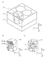
- FIG. 1A is a diagram illustrating a metal oxynitride film epitaxially grown on a substrate.
- FIG. 1B illustrates a crystal plane of a crystal included in the metal oxynitride film.
- FIG. 1C is a diagram illustrating an atomic arrangement of the crystal.
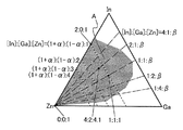
- FIG. 2 is a diagram for explaining the range of the atomic ratio of the metal constituting the oxide target.
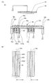
- FIGS. 3A and 3B are schematic views illustrating a sputtering apparatus.
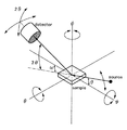
- FIG. 4 is an experimental arrangement diagram in the wide area reciprocal lattice space mapping and pole measurement.
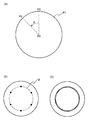
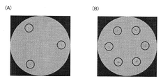
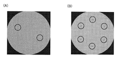
- FIG. 5A is a diagram illustrating a polar figure.
- FIGS. 5B and 5C are diagrams illustrating the intensity distribution obtained by the pole measurement.
- FIGS. 1A is a diagram illustrating a metal oxynitride film epitaxially grown on a substrate.
- FIG. 1B illustrates a crystal plane of a crystal included in the metal oxynit
- FIGS. 6A and 6B are diagrams illustrating a configuration example of a light-emitting element.
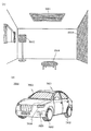
- 7A and 7B illustrate a lighting device according to one embodiment of the present invention.
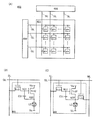
- 8A to 8C are diagrams illustrating a configuration example of a display device.
- FIGS. 9A to 9E are diagrams illustrating configuration examples of electronic devices.
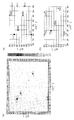
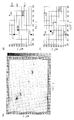
- FIG. 10A is a diagram illustrating a wide area reciprocal lattice space map of the sample 1 of the example.
- FIGS. 10B and 10C are diagrams showing a wide area reciprocal lattice space map obtained by simulation.
- FIGS. 11A and 11B are diagrams showing the results of the pole measurement for the sample 1 of the example.
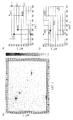
- FIG. 12A is a diagram showing a wide area reciprocal lattice space map of the sample 2 of the example.
- FIGS. 12B and 12C are diagrams showing a wide area reciprocal lattice space map obtained by simulation.
- FIGS. 13A and 13B are diagrams showing the results of the pole measurement on the sample 2 of the example.
- FIG. 14A is a diagram showing a wide area reciprocal lattice space map of the sample 3 of the example.
- FIGS. 14B and 14C are diagrams showing a wide area reciprocal lattice space map obtained by simulation.
- FIGS. 15A and 15B are diagrams showing the results of the pole measurement for the sample 3 of the example.
- FIG. 16A is a diagram showing a wide area reciprocal lattice space map of the sample 4 of the example.
- FIGS. 16B and 16C are diagrams showing a wide area reciprocal lattice space map obtained by simulation.
- FIGS. 17A and 17B are diagrams showing the results of the pole measurement for the sample 4 of the example.
- FIG. 18A is a diagram showing a wide area reciprocal lattice space map of the sample 5 of the example.
- FIGS. 18B and 18C are diagrams showing a wide area reciprocal lattice space map obtained by simulation.
- FIGS. 19A and 19B are diagrams showing the results of the pole measurement on the sample 5 of the example.
- FIG. 19A and 19B are diagrams showing the results of the pole measurement on the sample 5 of the example.
- FIGS. 20A is a diagram showing a wide area reciprocal lattice space map of the sample 6 of the example.
- FIGS. 20B and 20C are diagrams showing a wide area reciprocal lattice space map obtained by simulation.
- FIGS. 21A and 21B are diagrams showing the results of the pole measurement for the sample 6 of the example.
- FIG. 22A is a diagram showing a wide area reciprocal lattice space map of the sample 7 of the example.
- FIGS. 22B and 22C are diagrams showing the wide area reciprocal lattice space map obtained by the simulation.
- FIGS. 23A and 23B are diagrams showing the results of the pole measurement of the sample 7 of the example.
- ⁇ ⁇ Particular components may be omitted in some cases, particularly in a top view (also referred to as a “plan view”) or a perspective view, in order to facilitate understanding of the invention.
- a top view also referred to as a “plan view”
- a perspective view in order to facilitate understanding of the invention.
- some hidden lines and the like may be omitted.
- connection relation is not limited to the predetermined connection relation, for example, the connection relation shown in the figure or the text, and it is assumed that anything other than the connection relation shown in the figure or the text is disclosed in the figure or the text.
- X and Y are objects (for example, devices, elements, circuits, wirings, electrodes, terminals, conductive films, layers, and the like).
- a transistor is an element having at least three terminals including a gate, a drain, and a source.
- a region (hereinafter, also referred to as a channel formation region) in which a channel is formed between the drain (drain terminal, drain region, or drain electrode) and the source (source terminal, source region, or source electrode); A current can flow between the source and the drain through the channel formation region.
- a channel formation region refers to a region through which current mainly flows.
- the functions of the source and the drain may be switched when transistors having different polarities are used or when the direction of current changes in circuit operation. Therefore, in this specification and the like, the terms of source and drain may be used interchangeably.
- the term “insulator” can be replaced with an insulating film or an insulating layer.
- the term “conductor” can be referred to as a conductive film or a conductive layer.
- the term “semiconductor” can be referred to as a semiconductor film or a semiconductor layer.
- parallel refers to a state where two straight lines are arranged at an angle of ⁇ 10 ° or more and 10 ° or less. Therefore, a case where the angle is ⁇ 5 ° or more and 5 ° or less is also included.
- substantially parallel refers to a state in which two straight lines are arranged at an angle of ⁇ 30 ° or more and 30 ° or less.
- “Vertical” refers to a state in which two straight lines are arranged at an angle of 80 ° or more and 100 ° or less. Therefore, a case where the angle is 85 ° or more and 95 ° or less is also included.
- substantially perpendicular refers to a state in which two straight lines are arranged at an angle of 60 ° or more and 120 ° or less.
- a crystal plane is represented using a Miller index.
- the Miller index is indicated by three integers in parentheses.
- the direction in which the crystal planes are arranged is called the crystal orientation.
- the crystal orientation is indicated by three square brackets.
- a crystal plane is represented by (111), and a crystal orientation is represented by [111].
- Miller-Bravais index may be used.
- the plane index of the hexagonal lattice is represented by (hkil) using four integers (h, k, i, l).
- i ⁇ (h + k). Since the index i can be calculated from the values of the index h and the index k, in this specification, the hexagonal crystal plane is also represented by the Miller index (hkl) using three integers.
- a crystal plane appearing on the surface of a single crystal substrate may be referred to as a plane orientation of the single crystal substrate.
- lattice points (also referred to as reciprocal lattice points) in the reciprocal lattice corresponding to the crystal planes are represented by indices without parentheses.
- a reciprocal lattice point 111 shown in a spot observed in the wide area reciprocal lattice space map corresponds to the crystal plane (111).
- planes equivalent to (111) include (-111), (1-11), (11-1), and the like. In this specification, when (111) is described, (111) may include equivalent surfaces such as (-111), (1-11), and (11-1).
- Metal oxynitrides containing metal, oxygen, and nitrogen have attracted attention as semiconductor materials and insulating materials used for semiconductor devices. It is preferable that the metal oxynitride used for the semiconductor device has few impurities and defects and high stability.
- the stability of the metal oxynitride is high means that the metal oxynitride hardly reacts with a material in contact with the metal oxynitride due to heat generation accompanying operation of the semiconductor device, and the crystallinity of the metal oxynitride does not change. Defects are less likely to occur in the metal oxynitride.
- reliability of the semiconductor device can be improved.
- the impurities in the metal oxynitride refer to, for example, those other than the main components constituting the metal oxynitride.
- an element whose concentration is less than 0.1 atomic% can be regarded as an impurity.
- the element include hydrogen, silicon, boron, phosphorus, carbon, and transition metals other than the main components of metal oxynitride.
- the defects in the metal oxynitride are lattice defects, for example, point defects such as oxygen deficiency and nitrogen deficiency, line defects such as dislocations, and plane defects such as crystal grain boundaries. Defects in metal oxynitride include void defects such as voids.
- thin films include in-plane oriented thin films, oriented thin films, non-oriented thin films (polycrystalline thin films), and amorphous thin films (amorphous thin films).
- An oriented thin film is a thin film in which at least one crystal axis is aligned in a specific direction in crystals included in the thin film.
- An in-plane oriented thin film is a thin film in which three crystal axes are aligned in a specific direction in a crystal included in the thin film.
- the metal oxynitride thin film used for a semiconductor device or the like is preferably an oriented metal oxynitride thin film, and more preferably an in-plane oriented metal oxynitride thin film.
- the in-plane oriented metal oxynitride thin film has few impurities and defects and has a dense structure. Therefore, by using a metal oxynitride thin film with in-plane orientation for a semiconductor device or the like, the reliability of the semiconductor device or the like can be improved.
- Epitaxial growth is known as a method of forming an in-plane oriented thin film.
- Epitaxial growth means that crystals constituting a thin film grow on a single crystal substrate with a certain crystal orientation relationship. Note that growing a crystal having the same lattice constant as a crystal of the substrate on the single crystal substrate using the same material as the substrate is referred to as homoepitaxial growth.
- growth of a crystal on a single crystal substrate using a material different from that of the substrate or using a material different from the lattice constant of the crystal of the substrate is referred to as heteroepitaxial growth. Heteroepitaxial growth can be achieved by selecting a material having a small lattice mismatch with the crystal of the substrate, providing a layer (also called a buffer layer) for relaxing lattice distortion between the substrate and the thin film, or the like.
- Epitaxial growth methods include solid phase epitaxial growth (SPE: Solid Phase Epitaxy), liquid phase epitaxy (LPE: Liquid Phase Epitaxy), and vapor phase epitaxial growth (VPE: Vapor Phase Epitaxy).
- SPE Solid Phase Epitaxy
- LPE Liquid Phase Epitaxy
- VPE Vapor Phase Epitaxy
- the SPE method is a method in which a thin film is formed on the surface of a substrate, and the thin film is heated by electron beam irradiation or the like to change the crystal structure of the thin film into the same crystal structure as that of the substrate.
- the LPE method is a method of depositing a crystal part on a substrate surface from a supersaturated solution.
- the VPE method is a method of depositing components in a gas phase on a substrate surface.
- the VPE method includes a pulsed laser deposition (PLD: Pulsed Laser Deposition) method, an atomic layer deposition (ALD: Atomic Layer Deposition) method, a molecular beam epitaxial growth (MBE: Molecular Beam Epitaxy) method, and the like.
- the MBE method is a method in which an element or a material containing the element constituting a target crystal is heated and evaporated in an ultra-high vacuum, and the crystal is deposited on a heated substrate.
- the thin film is formed at a high temperature
- a heat treatment is performed at a high temperature (for example, 1000 ° C. or higher) after the thin film is formed, and the substrate surface is flattened before the thin film is formed.
- Coating providing one or more buffer layers on the substrate, selecting a substrate having a close lattice constant or thermal expansion coefficient, and the like.
- planarization treatment of the substrate surface for example, heat treatment is performed on the substrate at a high temperature.
- one embodiment of the present invention is a method for manufacturing a metal oxynitride film, in which a metal oxynitride film is epitaxially grown at a low temperature.
- the manufacturing method is a method in which a gas is introduced into a reaction chamber on a single crystal substrate, and a metal oxynitride film is epitaxially grown by a sputtering method.
- one embodiment of the present invention is a manufacturing method in which an in-plane oriented film is formed by epitaxial growth; therefore, a film epitaxially grown by the manufacturing method is an in-plane oriented film.
- the crystal structure of the metal oxynitride film to be epitaxially grown is preferably a hexagonal crystal structure.
- a wurtzite structure is particularly preferable.
- the wurtzite structure has a crystal orientation relationship that allows epitaxial growth with respect to a cubic system (for example, a diamond structure, a fluorite structure, a zinc blend structure, and the like).
- a cubic system for example, a diamond structure, a fluorite structure, a zinc blend structure, and the like.
- [111] of the cubic system and [001] of the wurtzite structure have a crystal orientation relationship capable of epitaxial growth.
- a metal oxynitride film having a hexagonal crystal structure can be easily epitaxially grown on a single crystal substrate having a cubic crystal system, a hexagonal crystal system, or the like. Further, a material having a crystal structure such as a cubic system and a hexagonal system can be easily grown on the metal oxynitride film.
- an insulating substrate such as a sapphire substrate or a stabilized zirconia substrate (such as a yttria-stabilized zirconia (YSZ) substrate) can be used.
- a YSZ substrate having a plane orientation of (111) or an A-plane sapphire substrate having a plane orientation of (110) may be used as the substrate.
- a YSZ substrate or an A-plane sapphire substrate as the substrate, it becomes easy to form a metal oxynitride thin film having a wurtzite-type crystal and having in-plane orientation.
- a semiconductor substrate formed using silicon, germanium, silicon carbide, gallium nitride, gallium arsenide, indium phosphide, or zinc oxide may be used.
- the difference between the lattice constant of the crystal of the thin film grown epitaxially and the lattice constant of the crystal of the substrate is preferably small. By reducing the lattice mismatch, a thin film can be easily grown epitaxially on a single crystal substrate.
- Lattice mismatch ⁇ a is the lattice constant a e of the crystal thin film epitaxially grown, the lattice constant a s of the substrate crystal and is calculated from the following equation (1).
- the degree of lattice mismatch between the metal oxynitride film to be epitaxially grown and the single crystal substrate is preferably 15% or less, more preferably 10% or less.
- the metal oxynitride film can be easily grown epitaxially on the single crystal substrate.
- the crystal orientation of the substrate surface is [111] and the metal oxynitride Since the crystal orientation of the surface of the material film is [001], the crystal orientations of the substrate and the metal oxide film are different. Therefore, a s a by root 2 times the value of 2 minutes lattice constant of the crystal of the substrate, it is possible to calculate the degree of lattice mismatch.
- the lattice constant of the crystal of the metal oxynitride film in the a-axis direction is preferably 0.31 nm or more and 0.41 nm or less, and 0.32 nm or more and 0.40 nm. The following is more preferred.
- FIG. 1A is a schematic view of a structure including a metal oxynitride film epitaxially grown on a single crystal substrate.
- FIG. 1A is a schematic diagram of a structure in which a metal oxynitride film 20 is formed on a single-crystal substrate 10.
- FIG. 1A illustrates a case where the metal oxynitride film 20 has a crystal 30 having a wurtzite structure.
- the metal oxynitride film is formed so that the c-axis ([001]) direction of the crystal 30 having a wurtzite structure matches the normal direction of the surface of the single crystal substrate 10. 20 is epitaxially grown.
- a c-axis ([001]) direction of a crystal included in the film matches a normal direction of a substrate surface of a single crystal.
- a film epitaxially grown by the manufacturing method of one embodiment may be referred to as a c-axis epitaxial film.
- FIG. 1B shows typical crystal planes ((001) plane and (101) plane) of the wurtzite structure.
- the (001) plane of the wurtzite structure shown in FIG. 1B is a plane parallel to the surface of the single crystal substrate 10.
- Fig. 1 (C) shows the arrangement of atoms in the wurtzite structure.
- the arrangement X1 in FIG. 1C is an arrangement of metal atoms
- the arrangement X2 is an arrangement of an oxygen atom or a nitrogen atom. Note that the arrangement X1 may be an arrangement of oxygen atoms or nitrogen atoms, and the arrangement X2 may be an arrangement of metal atoms.
- the sputtering target used for the above sputtering method is preferably an oxide target containing zinc, and more preferably an oxide target containing at least one of indium and gallium and zinc.
- the oxide target include a zinc oxide target, an indium zinc oxide (In-Zn oxide) target, a gallium zinc oxide (Ga-Zn oxide) target, and an indium gallium zinc oxide (In-Ga-Zn oxide).
- Object A target or the like can be used.
- an indium gallium zinc oxide target is preferably used as the oxide target.
- the crystal structures of indium nitride, gallium nitride, and zinc oxide are all wurtzite structures. Therefore, when a film is formed using the oxide target, a metal oxynitride thin film having a wurtzite-type structure and in-plane orientation can be easily formed.
- FIG. 2 is a diagram illustrating an atomic ratio of indium, gallium, and zinc included in the oxide target.
- FIG. 2 does not describe the atomic ratio of oxygen.
- the terms of the atomic ratios of indium, gallium, and zinc included in the oxide target are [In], [Ga], and [Zn].
- a region A shown in FIG. 2 shows an example of a preferable range of the atomic ratio of indium, gallium, and zinc contained in the oxide target.
- the sputtering target used in the above sputtering method is not limited to an oxide target, and may be an oxynitride target.
- an oxynitride target for example, an indium gallium zinc oxynitride (In-Ga-Zn oxynitride) target, an indium gallium oxynitride (In-Ga oxynitride) target, an indium zinc oxynitride (In-Zn) Oxynitride) target or the like can be used.
- the substrate temperature during the formation of the metal oxynitride film is preferably room temperature (25 ° C.) or more and 500 ° C. or less, more preferably 80 ° C. or more and 400 ° C. or less, and 100 ° C. or more and 250 ° C. or less. More preferably, there is. Since the film can be formed at a substrate temperature of 500 ° C. or lower, productivity of a semiconductor device or the like using the metal oxynitride film can be increased.
- a gas containing nitrogen gas as the gas introduced into the reaction chamber during the formation of the metal oxynitride film.
- the gas it is preferable to use a nitrogen gas, a mixed gas of a nitrogen gas and an oxygen gas, a mixed gas of a nitrogen gas and a rare gas (eg, argon or helium), or the like.
- the flow rate of the nitrogen gas is preferably 50% to 100% of the total flow rate of the gas.
- the composition of the obtained metal oxynitride film can be adjusted by adjusting the flow rate ratio of the nitrogen gas to the flow rate of the gas.
- a metal oxynitride film can be epitaxially grown without providing a buffer layer between the substrate and the thin film.
- FIG. 3A is a cross-sectional view illustrating a film forming chamber 41 included in a sputtering device
- FIG. 3B is a plan view of a magnet unit 54a and a magnet unit 54b included in the sputtering device.
- the film formation chamber 41 shown in FIG. 3A includes a target holder 52a, a target holder 52b, a backing plate 50a, a backing plate 50b, a sputtering target 70a, a sputtering target 70b, a member 58, and a substrate holder 62.
- the sputtering target 70a is disposed on the backing plate 50a.
- the backing plate 50a is disposed on the target holder 52a.
- the magnet unit 54a is disposed below the sputtering target 70a via the backing plate 50a.
- the sputtering target 70b is disposed on the backing plate 50b.
- the backing plate 50b is disposed on the target holder 52b.
- the magnet unit 54b is disposed below the sputtering target 70b via the backing plate 50b.
- the magnet unit 54a includes a magnet 54N1, a magnet 54N2, a magnet 54S, and a magnet holder 56.
- the magnet 54N1, the magnet 54N2, and the magnet 54S are arranged on the magnet holder 56. Further, the magnet 54N1 and the magnet 54N2 are arranged at an interval from the magnet 54S.
- the magnet unit 54b has the same structure as the magnet unit 54a.
- the sputtering target 70a, the backing plate 50a, and the target holder 52a are separated from the sputtering target 70b, the backing plate 50b, and the target holder 52b by a member 58.
- the member 58 is preferably an insulator.
- the member 58 may be a conductor or a semiconductor.
- the member 58 may be a conductor or a semiconductor whose surface is covered with an insulator.
- the target holder 52a and the backing plate 50a are fixed using screws (bolts or the like), and have the same potential.
- the target holder 52a has a function of supporting the sputtering target 70a via the backing plate 50a.
- the target holder 52b and the backing plate 50b are fixed using screws (bolts or the like) and have the same potential.
- the target holder 52b has a function of supporting the sputtering target 70b via the backing plate 50b.
- the backing plate 50a has a function of fixing the sputtering target 70a.
- the backing plate 50b has a function of fixing the sputtering target 70b.
- FIG. 3A the lines of magnetic force 64a and the lines of magnetic force 64b formed by the magnet unit 54a are clearly shown.
- the magnet unit 54a includes a rectangular or substantially rectangular magnet 54N1, a rectangular or substantially rectangular magnet 54N2, and a rectangular or substantially rectangular magnet 54S fixed to the magnet holder 56. It has the configuration that has been. Then, the magnet unit 54a can be swung right and left as indicated by the arrow shown in FIG. For example, the magnet unit 54a may be swung at a beat of 0.1 Hz or more and 1 kHz or less (it may be rephrased as a rhythm, a beat, a pulse, a frequency, a cycle, a cycle, etc.).
- the magnetic field on the sputtering target 70a changes with the swing of the magnet unit 54a. Since the region where the magnetic field is strong is a high-density plasma region, the sputtering phenomenon of the sputtering target 70a is likely to occur near the region. This is the same for the magnet unit 54b.
- FIGS. 3A and 3B illustrate an example in which a parallel-plate sputtering device is used; however, a method for forming a metal oxynitride film according to this embodiment is not limited thereto. is not.
- a metal oxynitride film may be formed using a facing target type sputtering apparatus.
- a method for forming a metal oxynitride film by epitaxial growth at a low temperature can be provided. Further, according to one embodiment of the present invention, a method can be provided in which a metal oxynitride film is formed by epitaxial growth without performing high-temperature treatment before and after the formation of the metal oxynitride film. According to one embodiment of the present invention, a semiconductor device or the like using a metal oxynitride film formed by epitaxial growth can be provided. Further, according to one embodiment of the present invention, productivity of a semiconductor device or the like using a metal oxynitride film can be increased.
- the evaluation of the epitaxial growth can be performed during the formation of the thin film or after the formation of the thin film, depending on the evaluation method.
- the epitaxial growth (crystallinity and orientation) of the formed thin film can be performed by a reciprocal lattice space mapping, a wide area reversal method in a transmission electron microscope (TEM), an X-ray diffraction (XRD) method, or an X-ray diffraction (XRD) method. It can be evaluated by a combination of lattice space mapping (WRSM: Wide-angle Reciprocal Space Mapping), pole measurement, Out-of-Plane measurement, In-Plane measurement, and the like.
- TEM transmission electron microscope
- XRD X-ray diffraction
- XRD X-ray diffraction
- the reciprocal lattice space is a space formed by basic vectors (also called reciprocal lattice vectors) of the reciprocal lattice space, and reflects the periodicity of the real space.
- the reciprocal lattice vector b j has the relationship of the following equation (2) with the basic vector a i of the real space lattice.
- ⁇ i, j is the Kronecker delta. That is, a plane defined in the crystal in the real space is treated as a lattice point in the reciprocal lattice.
- the epitaxially grown thin film has a small variation in the crystal orientation of the crystals constituting the thin film, that is, has a high orientation. Therefore, when the reciprocal lattice space map is obtained for the epitaxially grown thin film, the observed spot intensity is high and the half width of the spot is small. On the other hand, when the reciprocal lattice space map is obtained for a thin film having a large crystal orientation variation, that is, a thin film with low orientation, the observed spot intensity is low and the spot half width is large. As described above, by obtaining the reciprocal lattice space map, the crystallinity and orientation of the thin film can be evaluated.
- the wide area reciprocal lattice space mapping using the X-ray analyzer will be described with reference to FIG.
- the direction in which the X-ray source source, the sample sample, and the detector are arranged in a line is defined as the ⁇ axis.
- the direction perpendicular to the ⁇ axis is defined as the ⁇ axis.
- a direction perpendicular to the ⁇ axis and the ⁇ axis is defined as a ⁇ axis. That is, the ⁇ axis is parallel to the direction in which the X-ray analyzer is viewed from above.
- a ⁇ axis may be a ⁇ axis depending on the device. Therefore, the ⁇ axis can be rephrased as the ⁇ axis.
- the axis used as the ⁇ axis in this specification may be the ⁇ axis depending on the device. Therefore, the ⁇ axis can be rephrased as the ⁇ axis.
- a two-dimensional detector In the wide area reciprocal space mapping, a two-dimensional detector is used as a detector.
- the two-dimensional detector has position information for the 2 ⁇ and ⁇ directions on the detection surface. Note that the detector detector shown in FIG. 4 is a model of a two-dimensional detector.
- the wide area reciprocal space mapping is performed by operating the sample and the detector when the X-ray source is fixed.
- the detector can be tilted in the 2 ⁇ direction, and the sample can be tilted in the ⁇ direction, the ⁇ direction, and the ⁇ direction.
- the wide area reciprocal lattice space mapping is a measurement technique in which a sample is tilted stepwise in the ⁇ direction and 2 ⁇ / ⁇ scans are executed at each ⁇ position (angle). This makes it possible to acquire a wide area reciprocal space map in which a wide range in the reciprocal space is measured.
- the wide area reciprocal lattice space mapping is performed by operating the X-ray source, the sample, and the detector.
- the X-ray source source can be tilted in the ⁇ direction.
- CuK ⁇ radiation (wavelength: 0.15418 nm) is used as an X-ray source.
- a wide area reciprocal space map is simulated.
- software “SMAP / for ⁇ Cross ⁇ Sectional ⁇ XRD-RSM” provided by Bruker Japan can be used.
- a wide area reciprocal lattice space map corresponding to the input values is output.
- the peak of the spot corresponding to the reciprocal lattice point 002 is preferably located at an angle 2 ⁇ of 30 ° or more and 35 ° or less and an angle ⁇ of about 0 °.
- the peak of the spot corresponding to the reciprocal lattice point 101 preferably has an angle 2 ⁇ of 33 ° to 37 ° and an angle ⁇ of 61 ° to 65 °.
- the half width of the spot corresponding to reciprocal lattice point 002 and reciprocal lattice point 101 is preferably less than 2 °.
- the pole measurement is a method of measuring the diffraction intensity distribution by rotating the sample in all directions while keeping the position (angle) of the X-ray source and the detector constant.
- a two-dimensional detector is used as a detector in this specification. Specifically, the detector is fixed at the detection angle (2 ⁇ ), and the sample sample is rotated in the in-plane direction ( ⁇ direction) while the sample sample is tilted in the ⁇ direction and the ⁇ direction, and the grating surface is tilted in all directions. Is measured. From the diffraction intensity obtained by the pole measurement, the crystallinity and orientation of the thin film can be evaluated.
- the detector used for the pole measurement is not limited to the two-dimensional detector, but may be a zero-dimensional detector.
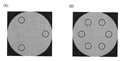
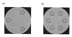
- FIG. 5A shows a polar figure. As shown in FIG. 5 (A), the center P0 of the polar figure has an angle ⁇ of 0 °, and the outer periphery P1 of the polar figure has an angle 90 of 90 °.
- a straight line (a straight line indicated by a dashed line P0-P2 in FIG.
- FIGS. 5B and 5C show schematic diagrams of diffraction intensity obtained by pole measurement.
- FIG. 5B is a schematic diagram of diffraction intensity when a spot-like intensity distribution is observed on a concentric circle having an angle ⁇ (a circle shown by a dashed line in the figure).
- FIG. 4 is a schematic diagram of diffraction intensity when a ring-shaped intensity distribution is observed.
- the (101) plane of the wurtzite structure has sixfold symmetry. That is, when pole measurement is performed on a c-axis epitaxial film having a crystal having a wurtzite structure, as shown in FIG. (Diffraction peak) is observed. Therefore, when a thin film having a crystal having a wurtzite structure is epitaxially grown on the c-axis, a diffraction peak showing six-fold symmetry is observed by ⁇ scan of the crystal of the thin film with respect to the (101) plane in pole measurement. Specifically, a diffraction peak is observed at about every 60 ° with respect to the angle ⁇ on a concentric circle having an angle ⁇ of about 62 °.
- a diffraction peak showing three-fold symmetry is observed in the pole scan. Specifically, a diffraction peak is observed at about 120 ° with respect to the angle ⁇ on a concentric circle having an angle ⁇ of about 70 °. Further, in the pole measurement, in the ⁇ scan with respect to the (104) plane of the single-crystal A-plane sapphire substrate, a diffraction peak showing two-fold symmetry is observed. Specifically, a diffraction peak is observed at about 180 ° with respect to the angle ⁇ on a concentric circle having an angle ⁇ of about 58 °.
- the measurement using the XRD method includes an out-of-plane measurement and an in-plane measurement.
- Out-of-plane measurement is a method for evaluating a crystal plane parallel to the surface of the thin film
- in-plane measurement is a method for evaluating a crystal plane perpendicular to the surface of the thin film.
- a 0-dimensional detector may be used as a detector.
- the metal oxynitride film include, for example, light-emitting elements, light-receiving elements, and semiconductor devices.
- a light-emitting element also referred to as a light-emitting diode or LED.
- FIGS. 6A and 6B illustrate a light-emitting element 100 using a metal oxynitride film according to one embodiment of the present invention.
- the light emitting element 100 includes a substrate 102, an n-type cladding layer 104, an active layer 106, a p-type cladding layer 108, and an n-type electrode 110. And a p-type electrode 112.
- the active layer 106 is sandwiched between the n-type cladding layer 104 and the p-type cladding layer 108.
- the active layer 106 electrons and holes are combined to emit light. That is, the active layer 106 can be called a light-emitting layer.
- the stacked structure including the n-type cladding layer 104, the active layer 106, and the p-type cladding layer 108 is formed so as to emit light of red, yellow, green, blue, or the like.
- the laminated structure includes a gallium / phosphorus compound, a gallium / arsenic compound, a gallium / aluminum / arsenic compound, an aluminum / gallium / indium / phosphorous compound, a gallium nitride, an indium / gallium nitride compound, a selenium / zinc compound, and the like.
- a gallium / phosphorus compound a gallium / arsenic compound, a gallium / aluminum / arsenic compound, an aluminum / gallium / indium / phosphorous compound, a gallium nitride, an indium / gallium nitride compound, a selenium / zinc compound, and the like.
- the flow rate of nitrogen gas introduced into the reaction chamber at the time of film formation, the conductivity of the metal oxynitride film, (Or insulating property), band gap, light transmittance, and the like can be adjusted.
- the conductivity of the film tends to increase as the flow rate of the nitrogen gas increases. Therefore, by adjusting the conductivity of the metal oxynitride film, the n-type cladding layer 104 shown in FIG. 6A or the n-type electrode shown in FIG. 110 can be used.
- the metal oxynitride film may be used for the n-type electrode 110 and the n-type cladding layer 104 shown in FIG.
- the metal oxynitride film is formed while adjusting the flow rate of nitrogen gas.
- the n-type electrode 110 and the n-type cladding layer 104 shown in FIG. 6B can be continuously formed.
- the metal oxynitride film can function as a buffer layer for epitaxially growing a thin film on the film. Therefore, the crystallinity of the n-type cladding layer 104 or the active layer 106 formed on the metal oxynitride film can be improved.
- the crystal structure of the metal oxynitride film is a hexagonal system, and particularly a wurtzite crystal structure. Therefore, for the n-type cladding layer 104 or the active layer 106 formed over the metal oxynitride film, a material which forms a wurtzite crystal structure such as gallium nitride or an indium / gallium nitride compound is preferably used. .
- the metal oxynitride film has a function as a base (buffer layer) for growing a hexagonal crystal and also has a function as an n-type electrode or an n-type cladding layer.
- the metal oxynitride film for the n-type electrode 110 or the n-type cladding layer 104, the n-type cladding layer 104 or the active layer 106 can be easily epitaxially grown, and the crystal of the n-type cladding layer 104 or the active layer 106 can be easily formed.
- characteristics of the light-emitting element such as luminous efficiency and durability can be improved.
- FIG. 7A illustrates an example in which a light-emitting element is used as an indoor lighting device.
- a large-area lighting device 8501 and a lighting device 8502 having a curved surface can be formed.
- a large-sized lighting device 8503 may be provided on a wall surface in the room.
- a touch sensor may be provided for the lighting device 8501, the lighting device 8502, and the lighting device 8503, so that the power is turned on or off.
- the lighting device 8504 having a table function can be obtained. Note that by using a light-emitting element for part of other furniture, a lighting device having a function as furniture can be obtained.
- a light-emitting device to which the light-emitting element of one embodiment of the present invention is applied can be applied to lighting of a car, for example, lighting can be installed on a dashboard, a windshield, a ceiling, or the like.
- FIG. 7B shows an appearance of an automobile 7900.
- the car 7900 includes a car body 7901, wheels 7902, a windshield 7903, a light 7904, a fog lamp 7905, and the like.
- the light-emitting element of one embodiment of the present invention can be used for the light 7904 and the fog lamp 7905 illustrated in FIG. 7B, for example. Further, for example, although not shown, it can be used for a side blinker, a back lamp, a door courtesy lamp, and the like.
- a lighting device can be obtained by applying the light-emitting element of one embodiment of the present invention.
- applicable lighting devices are not limited to those described in this embodiment, and can be applied to lighting devices in all fields.
- the display device of this embodiment has a function of displaying an image using a light-emitting element.
- a micro light emitting diode hereinafter, also referred to as a micro LED
- micro LEDs as display elements
- power consumption of the display device can be reduced.
- the display device can be reduced in thickness and weight.
- a display device using a micro LED as a display element has high contrast and a wide viewing angle, so that display quality can be improved.
- Area of the region for emitting micro LED light is preferably 1 mm 2 or less, more preferably 10000 2 or less, more preferably 3000 .mu.m 2 or less, more preferably 700 .mu.m 2 or less.
- FIG. 8A illustrates a configuration example of a display device 400 using a light-emitting element.
- the display device 400 includes a pixel portion 401, a driver circuit 402, and a driver circuit 403.
- the pixel unit 401 includes a plurality of pixels pix.
- the pixel pix is connected to the wiring SL and the wiring GL, respectively.
- the wirings GL are each connected to the driving circuit 402, and the wirings SL are each connected to the driving circuit 403.
- a selection signal is supplied to the wiring GL, and a video signal is supplied to the wiring SL.
- the drive circuit 402 has a function of supplying a selection signal to the pixel pix. Specifically, the driving circuit 402 has a function of supplying a selection signal to the wiring GL, and the wiring GL has a function of transmitting the selection signal output from the driving circuit 402 to the pixel pix.
- the driver circuit 402 can be referred to as a gate driver circuit or a gate driver, and the wiring GL can be referred to as a selection signal line, a gate line, or the like.
- the driving circuit 403 has a function of supplying a video signal to the pixel pix. Specifically, the driving circuit 403 has a function of supplying a video signal to the wiring SL, and the wiring SL has a function of transmitting a video signal output from the driving circuit 403 to the pixel pix.
- the driver circuit 403 can be referred to as a source side driver circuit or a source driver, and the wiring SL can be referred to as a video signal line, a source line, or the like.
- FIG. 8B illustrates a configuration example of a pixel pix using a light-emitting element as a display element.
- the pixel pix illustrated in FIG. 8B includes a transistor Tr31, a transistor Tr32, a capacitor C31, and a light-emitting element LE.
- the transistors Tr31 and Tr32 are n-channel transistors here, but the polarity of the transistors can be changed as appropriate.
- the light-emitting element described in the above embodiment can be used for the light-emitting element LE.
- the gate of the transistor Tr31 is connected to the wiring GL, one of a source and a drain is connected to the gate of the transistor Tr32 and one electrode of the capacitor C31, and the other of the source and the drain is connected to the wiring SL.
- One of a source and a drain of the transistor Tr32 is connected to the other electrode of the capacitor C31 and one electrode of the light-emitting element LE, and the other of the source and the drain is connected to a wiring to which the potential Va is supplied.
- the other electrode of the light-emitting element LE is connected to a wiring to which the potential Vc is supplied.
- a node connected to one of the source and the drain of the transistor Tr31, the gate of the transistor Tr32, and one electrode of the capacitor C31 is referred to as a node N31.
- a node connected to one of the source and the drain of the transistor Tr32, the other electrode of the capacitor C31, and one electrode of the light-emitting element LE is referred to as a node N32.
- the potential Va is a high power supply potential and the potential Vc is a low power supply potential is described.
- Each of the potential Va and the potential Vc can be a common potential in a plurality of pixels pix.
- the capacitor C31 has a function as a storage capacitor for holding the potential of the node N31.
- the transistor Tr31 has a function of controlling supply of the potential of the wiring SL to the node N31. Specifically, by controlling the potential of the wiring GL to turn on the transistor Tr31, the potential of the wiring SL corresponding to the video signal is supplied to the node N31, and writing of the pixel pix is performed. After that, by controlling the potential of the wiring GL to turn off the transistor Tr31, the potential of the node N31 is held.
- the amount of current flowing between the source and the drain of the transistor Tr32 is controlled according to the voltage between the node N31 and the node N32, and the light emitting element LE emits light with luminance according to the amount of current. Thereby, the gradation of the pixel pix can be controlled.
- the transistor Tr32 preferably operates in a saturation region.
- the transistor Tr31 and the transistor Tr32 may be provided in the same layer or may be provided in a stacked manner.
- the transistor Tr31 and the transistor Tr32 can be manufactured at the same time, and the manufacturing process of the display device can be shortened.
- the degree of integration of the display device can be increased.
- a configuration in which two transistors (Tr31 and Tr32) are provided in the pixel pix is preferable. Note that one embodiment of the present invention is not limited thereto, and a structure including three or more transistors in a pixel pix may be employed.
- FIG. 8C is a configuration example of a pixel pix which uses a light-emitting element as a display element, which is different from FIG. 8B.
- the pixel pix illustrated in FIG. 8C includes a transistor Tr31, a transistor Tr32, a transistor Tr33, a capacitor C31, and a light-emitting element LE. That is, the pixel pix illustrated in FIG. 8C is a pixel in which a transistor Tr33 for monitoring the amount of current flowing through the transistor Tr32 is added to the pixel pix illustrated in FIG.
- the gate of the transistor Tr31 is connected to the wiring GL, one of a source and a drain is connected to the gate of the transistor Tr32 and one electrode of the capacitor C31, and the other of the source and the drain is connected to the wiring SL.
- One of a source and a drain of the transistor Tr32 is connected to the other electrode of the capacitor C31, one electrode of the light-emitting element LE, and one of a source and a drain of the transistor Tr33, and the other of the source and the drain is supplied with the potential Va.
- the other electrode of the light-emitting element LE is connected to a wiring to which the potential Vc is supplied.
- the gate of the transistor Tr33 is connected to the wiring GL, and the other of the source and the drain is connected to the monitor line ML.
- a node connected to one of the source and the drain of the transistor Tr31, the gate of the transistor Tr32, and one electrode of the capacitor C31 is referred to as a node N31.
- a node connected to one of the source and the drain of the transistor Tr32, the other electrode of the capacitor C31, the one electrode of the light-emitting element LE, and one of the source and the drain of the transistor Tr33 is referred to as a node N32.
- the wiring GL may be selected using a progressive method or an interlace method. Further, the supply of the video signal to the wiring SL may be performed by using dot sequential driving for sequentially supplying the video signal to the wiring SL, or may be performed by using the line sequential driving for supplying the video signal to all the wirings SL at once. You may go. Further, the video signal may be sequentially supplied to each of the plurality of wirings SL.
- an element belonging to Group 14 such as silicon or germanium, a compound semiconductor such as gallium arsenide, an organic semiconductor, or a metal oxide can be used.
- the semiconductor may be a non-single-crystal semiconductor (an amorphous semiconductor, a microcrystalline semiconductor, a polycrystalline semiconductor, or the like), or may be a single-crystal semiconductor.
- the transistor included in the pixel pix preferably includes an amorphous semiconductor in a channel formation region, particularly, hydrogenated amorphous silicon (a-Si: H). Since a transistor using an amorphous semiconductor can easily cope with an increase in the area of a substrate, a manufacturing process is required when a large-screen display device capable of supporting 4K2K broadcast, 8K4K broadcast, or the like is manufactured. It can be simplified.
- a-Si hydrogenated amorphous silicon
- ⁇ As a transistor included in the pixel pix a transistor including a metal oxide in a channel formation region (OS transistor) can be used.
- the OS transistor has higher field-effect mobility than a transistor using hydrogenated amorphous silicon. Further, a crystallization step which is necessary for a transistor using polycrystalline silicon or the like is not required.
- the frequency of updating the video signal can be set extremely low during a period in which the image displayed on the pixel portion 401 does not change or a period in which the change is equal to or less than a certain value.
- the frequency of updating the video signal can be set to, for example, once or less per 0.1 second, once or less per second, and once or less every 10 seconds.
- a large number of pixels pix are provided corresponding to 4K2K broadcast, 8K4K broadcast, or the like, it is effective to reduce power consumption by omitting updating of a video signal.
- Examples of the electronic device include a television device, a desktop or notebook personal computer, a monitor for a computer, a digital signage, an electronic device having a relatively large screen such as a large game machine such as a pachinko machine, and a digital device.
- Examples include a camera, a digital video camera, a digital photo frame, a mobile phone, a portable game machine, a portable information terminal, and a sound reproducing device.
- the electronic device of one embodiment of the present invention may include an antenna. By receiving a signal with the antenna, display of an image, information, or the like can be performed on the display portion.
- the display portion can be configured by a display device, and thus the display portion can also be called a display device.
- the antenna may be used for wireless power transmission.
- the electronic device of one embodiment of the present invention includes sensors (force, displacement, position, speed, acceleration, angular velocity, rotation speed, distance, light, liquid, magnetism, temperature, chemical substance, sound, time, hardness, electric field, current, (Including a function of measuring voltage, power, radiation, flow rate, humidity, gradient, vibration, smell, or infrared light).
- the electronic device of one embodiment of the present invention can have various functions. For example, a function of displaying various information (still images, moving images, text images, etc.) on the display unit, a touch panel function, a function of displaying a calendar, date or time, a function of executing various software (programs), a wireless communication It can have a function, a function of reading a program or data recorded on a recording medium, and the like.
- FIG. 9A illustrates an example of a television device.
- a display portion 7000 is incorporated in a housing 7101.
- a structure in which the housing 7101 is supported by the stand 7103 is shown.
- the display device of one embodiment of the present invention can be applied to the display portion 7000.
- the television device 7100 illustrated in FIG. 9A can be operated with an operation switch of the housing 7101 or a separate remote controller 7111.
- the display portion 7000 may be provided with a touch sensor, and may be operated by touching the display portion 7000 with a finger, a stylus, or the like.
- the remote controller 7111 may include a display unit that displays information output from the remote controller 7111. Channel and volume operations can be performed with operation keys or a touch panel included in the remote controller 7111, and images displayed on the display portion 7000 can be operated.
- the television set 7100 is provided with a receiver, a modem, and the like.
- a general television broadcast can be received by the receiver.
- by connecting to a wired or wireless communication network via a modem one-way (from sender to receiver) or two-way (between sender and receiver, between receivers, etc.) information communication can be performed. Is also possible.
- FIG. 9B illustrates a laptop personal computer 7200.
- the laptop personal computer 7200 includes a housing 7211, a keyboard 7212, a pointing device 7213, an external connection port 7214, and the like.
- a display portion 7000 is incorporated in the housing 7211.
- the display device of one embodiment of the present invention can be applied to the display portion 7000.
- FIGS. 9C and 9D show an example of digital signage.
- a digital signage 7300 illustrated in FIG. 9C includes a housing 7301, a display portion 7000, a speaker 7303, and the like. Further, it can have an LED lamp, an operation key (including a power switch or an operation switch), a connection terminal, various sensors, a microphone, and the like.
- FIG. 9D illustrates a digital signage 7400 attached to a column 7401.
- the digital signage 7400 has a display portion 7000 provided along the curved surface of the column 7401.
- the display device of one embodiment of the present invention can be applied to the display portion 7000.
- the digital signage 7300 or the digital signage 7400 can cooperate with the information terminal 7311 or the information terminal 7411 such as a smartphone possessed by the user by wireless communication.
- advertisement information displayed on the display portion 7000 can be displayed on the screen of the information terminal 7311 or the information terminal 7411.
- the display on the display portion 7000 can be switched by operating the information terminal 7311 or the information terminal 7411.
- the digital signage 7300 or the digital signage 7400 can also execute a game using the information terminal 7311 or the screen of the information terminal 7411 as an operation means (controller).
- an unspecified number of users can simultaneously participate in the game and enjoy it.
- the display device according to one embodiment of the present invention can be incorporated along an inner or outer wall of a house or a building, or a curved surface of an interior or exterior of a vehicle.
- FIG. 9E illustrates an example in which the display device according to one embodiment of the present invention is mounted on a vehicle.
- FIG. 9E illustrates a configuration example of a vehicle including the display portion 5001.
- a display device according to one embodiment of the present invention can be used.
- FIG. 9E illustrates an example in which the display portion 5001 is mounted on a right-hand drive vehicle.
- the display portion 5001 is not particularly limited and can be mounted on a left-hand drive vehicle. In this case, the arrangement on the left and right of the configuration shown in FIG.
- FIG. 9E shows a dashboard 5002, a handle 5003, a windshield 5004, and the like arranged around the driver's seat and the passenger's seat.
- the display unit 5001 is arranged at a predetermined position of the dashboard 5002, specifically, around the driver, and has a substantially T-shape.
- FIG. 9E illustrates an example in which one display portion 5001 formed using a plurality of display panels 5007 (display panels 5007a, 5007b, 5007c, and 5007d) is provided along a dashboard 5002.
- the display portion 5001 may be arranged at a plurality of locations.
- the plurality of display panels 5007 may have flexibility.
- the display portion 5001 can be processed into a complicated shape, and the display portion 5001 can be formed along a curved surface of the dashboard 5002 or the like, or can be displayed on a connection portion of a steering wheel, a display portion of an instrument, an air vent 5006, or the like.
- a configuration in which the display area of the portion 5001 is not provided can be easily realized.
- FIG. 9E illustrates an example in which the camera 5005 is provided instead of the side mirror, but both the side mirror and the camera may be provided.
- a CCD camera, a CMOS camera, or the like can be used.
- an infrared camera may be used in combination. Since the output level of the infrared camera increases as the temperature of the subject increases, the infrared camera can detect or extract a living body such as a human or an animal.
- the image captured by the camera 5005 can be output to one or more of the display panels 5007a, 5007b, 5007c, and 5007d.
- the display unit 5001 is mainly used to assist driving of the vehicle. By photographing the situation on the rear side with a wide angle of view using the camera 5005 and displaying the image on the display panel 5007, the driver can visually recognize the blind spot area, and the occurrence of an accident can be prevented.
- a distance image sensor may be provided on the roof of a car or the like, and an image obtained by the distance image sensor may be displayed on the display unit 5001.
- an image sensor, a lidar (Light Detection and Ranging), or the like can be used as the range image sensor.
- a lidar Light Detection and Ranging
- the display unit 5001 may have a function of displaying map information, traffic information, television images, DVD images, and the like.
- map information can be displayed large using the display panels 5007a, 5007b, 5007c, and 5007d as one display screen. Note that the number of display panels 5007 can be increased in accordance with the displayed video.
- the images displayed on the display panels 5007a, 5007b, 5007c, and 5007d can be freely set according to the driver's preference. For example, a television image and a DVD image are displayed on the left display panel 5007d, map information is displayed on the central display panel 5007b, instruments are displayed on the right display panel 5007c, and audio items are displayed near the transmission gear (driving gear). (Between the seat and the passenger seat) on the display panel 5007a. Further, by combining a plurality of display panels 5007, a fail-safe function can be added to the display portion 5001. For example, even if one display panel 5007 breaks down for some reason, the display area can be changed and display can be performed using another display panel 5007.
- samples 1 to 7 each having a metal oxynitride film formed on a substrate by the method described in the above embodiment are prepared, and a wide area reciprocal lattice space is provided for each sample. Mapping, pole measurement, Out-of-plane measurement, In-plane measurement, and the like were performed.
- Samples 1 to 7 were manufactured using the method for manufacturing a metal oxynitride film described in Embodiment 1. Specifically, a single crystal substrate was prepared, a gas was introduced into the reaction chamber over the substrate, and a metal oxynitride film was formed by a sputtering method using an oxide target. Note that before forming the metal oxynitride film on the substrate, pretreatment such as atmospheric annealing or vacuum annealing is not performed on the substrate. No heat treatment was performed on the formed metal oxynitride film.
- YSZ yttria-stabilized zirconia
- the metal oxynitride film of Sample 4 is an In-Ga-Zn oxynitride film.
- a gas (also referred to as a deposition gas) introduced into the reaction chamber will be described.
- a nitrogen gas (N 2 ) of 45 sccm was used.
- a mixed gas of nitrogen gas (N 2 ) 45 sccm and argon gas (Ar) 45 sccm was used as a deposition gas.
- the Out-of-plane measurement and the In-plane measurement are mainly performed to estimate a lattice constant used as an input value of a simulation of a wide area reciprocal space map. Therefore, in the present embodiment, illustration of the results of the out-of-plane measurement and the in-plane measurement is omitted.
- the angle 2 ⁇ was collectively estimated by a two-dimensional detector (detector in FIG. 4), and the angle ⁇ was scanned and measured at each angle ⁇ .
- the distance between the sample (the sample in FIG. 4) and the two-dimensional detector (the detector in FIG. 4) was set to about 150 mm.
- the angle 2 ⁇ was set to 40 °, and the range where the angle 2 ⁇ was 20 ° or more and 60 ° or less was recorded collectively.
- scanning was performed at an angle ⁇ of 10 ° or more and 30 ° or less.
- the angle ⁇ was set in a range of 0 ° to 85 ° in increments of 5 ° (a total of 18 steps).
- the incident X-ray diameter was 0.3 mm ⁇ using a collimator, CuK ⁇ rays (wavelength: 0.15418 nm) were used as the X-ray source, and the output of the X-ray was 50 kV and 100 mA.
- the X-ray exposure time per step was 60 seconds.
- Wide reciprocal space mapping was performed for each sample, and a wide reciprocal space map for each sample was obtained.
- the horizontal axis is an angle 2 ⁇ [°]
- the vertical axis is an angle ⁇ [°].
- the intensity at each point of the wide area reciprocal space map is represented in association with the bar shown on the right of the wide area reciprocal space map. Specifically, the higher the intensity, the darker (darker) the color, and the lower the intensity, the whiter (lighter) the color.
- the wide area reciprocal lattice space map obtained by the simulation shows all spots that can be observed in the crystal assumed in the simulation. Therefore, in the wide area reciprocal lattice space map of the epitaxially grown thin film and the wide area reciprocal lattice space map obtained by the simulation, the observed crystal spot may be different because the in-plane oriented crystal orientation may differ depending on the angle ⁇ .
- the angle ⁇ is adjusted, and the wide area reciprocal space mapping is performed. Specifically, in the samples 1 to 6, the (101) plane of the metal oxynitride film of each sample and the (111) plane of the substrate of each sample are simultaneously observed in the wide area reciprocal lattice space map. As described above, the wide area reciprocal lattice space mapping may be performed by adjusting the angle ⁇ .
- the angle ⁇ is set so that the (101) plane of the metal oxynitride film of the sample 7 and the (104) plane of the substrate of the sample 7 are simultaneously observed in the wide area reciprocal space map. It is good to perform wide area reciprocal lattice space mapping by adjusting.
- FIG. 10A shows a wide area reciprocal lattice space map of Sample 1.
- FIGS. 10B and 10C show a wide area reciprocal lattice space map obtained by the simulation.
- FIG. 10B is a wide area reciprocal space map corresponding to the single crystal substrate of Sample 1
- FIG. 10C is a wide area reciprocal space corresponding to the crystal of the metal oxynitride film of Sample 1. It is a map.
- FIG. 10 (A) a plurality of spots were observed.
- the spot where the peak is located at an angle 2 ⁇ of about 35 ° and an angle ⁇ of about 62 ° It can be seen that a spot corresponding to the (101) plane of the wurtzite structure and having a peak at an angle 2 ⁇ of about 44 ° and an angle ⁇ of about 44 ° corresponds to the (102) plane of the wurtzite structure.
- FIGS. 11A and 11B show the results of the pole measurement for Sample 1 in FIGS. 11A and 11B.
- FIG. 11A shows the result of the (111) plane of the single crystal substrate of Sample 1
- FIG. 11B shows the result of the (101) plane of the metal oxynitride film of Sample 1.
- ⁇ As shown by the solid circle in FIG. 11A spot-like intensity distributions were observed at three points on a concentric circle having an angle ⁇ of about 70 °.
- the spot is a three-fold symmetric spot derived from the (111) plane of yttria-stabilized zirconia (YSZ).
- spot-like intensity distributions were observed at six locations on a concentric circle having an angle ⁇ of about 62 °. That is, it can be seen that the (101) plane of the metal oxynitride film of Sample 1 has six-fold symmetry, and the metal oxynitride film of Sample 1 is in-plane oriented.
- FIGS. 11A and 11B show that the metal oxide film of Sample 1 is a c-axis epitaxial film which does not include a domain whose crystal orientation is rotated in the film plane.
- the metal oxynitride film of Sample 1 has a wurtzite structure and is epitaxially grown.
- FIG. 12A shows a wide area reciprocal lattice space map of Sample 2.
- FIGS. 12B and 12C show the wide area reciprocal lattice space map obtained by the simulation.
- FIG. 12B is a wide area reciprocal lattice space map corresponding to the single crystal substrate of Sample 2
- FIG. 12C is a wide area reciprocal lattice space corresponding to the crystal of the metal oxynitride film of Sample 2. It is a map.
- FIG. 12 (A) a plurality of spots were observed.
- the spots whose peaks are located at an angle 2 ⁇ of about 34 ° and an angle ⁇ of about 62 ° are: It can be seen that a spot corresponding to the (101) plane of the wurtzite structure and having a peak at an angle 2 ⁇ of about 44 ° and an angle ⁇ of about 44 ° corresponds to the (102) plane of the wurtzite structure.
- FIGS. 13A and 13B show the results of the pole measurement for Sample 2 in FIGS. 13A and 13B.
- FIG. 13A shows the result of the (111) plane of the single crystal substrate of Sample 2
- FIG. 13B shows the result of the (101) plane of the metal oxynitride film of Sample 2.
- spot-like intensity distributions were observed at three points on a concentric circle having an angle ⁇ of about 70 °. Further, as shown by the solid circle in FIG. 13B, spot-like intensity distributions were observed at six locations on a concentric circle having an angle ⁇ of about 62 °. That is, it can be seen that the (101) plane of the metal oxynitride film of Sample 2 has sixfold symmetry, and the metal oxynitride film of Sample 2 is in-plane oriented.
- FIGS. 13A and 13B show that the metal oxide film of Sample 2 is a c-axis epitaxial film that does not include a domain whose crystal orientation is rotated in the film plane.
- the metal oxynitride film of Sample 2 has a wurtzite structure and is epitaxially grown.
- FIG. 14A shows a wide area reciprocal lattice space map of Sample 3.
- FIGS. 14B and 14C show a wide area reciprocal lattice space map obtained by the simulation.
- FIG. 14B is a wide area reciprocal lattice space map corresponding to the single crystal substrate of Sample 3
- FIG. 14C is a wide area reciprocal lattice space corresponding to the crystal of the metal oxynitride film of Sample 3. It is a map.
- FIG. 14 (A) a plurality of spots were observed.
- the spots whose peaks are located at an angle 2 ⁇ of about 36 ° and an angle ⁇ of about 62 ° are: It can be seen that a spot corresponding to the (101) plane of the wurtzite structure and having a peak at an angle 2 ⁇ of about 47 ° and an angle ⁇ of about 42 ° corresponds to the (102) plane of the wurtzite structure.
- FIGS. 15A and 15B show the results of the pole measurement for Sample 3 in FIGS. 15A and 15B.
- FIG. 15A shows the result of the (111) plane of the single crystal substrate of Sample 3
- FIG. 15B shows the result of the (101) plane of the metal oxynitride film of Sample 3.
- spot-like intensity distributions were observed at three points on a concentric circle having an angle ⁇ of about 70 °.
- spot-like intensity distributions were observed at six locations on a concentric circle having an angle ⁇ of about 62 °.
- the (101) plane of the metal oxynitride film of Sample 3 has sixfold symmetry, and the metal oxynitride film of Sample 3 is in-plane oriented.
- the crystal of the metal oxynitride film of Sample 3 must have a wurtzite structure.
- the metal oxide film of Sample 3 is a c-axis epitaxial film that does not include a domain whose crystal orientation is rotated in the plane of the film.
- the metal oxynitride film of Sample 3 has a wurtzite structure and is epitaxially grown.
- FIG. 16A shows a wide area reciprocal lattice space map of the sample 4.
- FIGS. 16B and 16C show the wide area reciprocal lattice space map obtained by the simulation.
- FIG. 16B is a wide area reciprocal lattice space map corresponding to the single crystal substrate of Sample 4
- FIG. 16C is a wide area reciprocal lattice space corresponding to the crystal of the metal oxynitride film of Sample 4. It is a map.
- FIG. 16A a plurality of spots were observed.
- the spot where the peak is located at an angle 2 ⁇ of about 35 ° and an angle ⁇ of about 62 ° is: It can be seen that a spot corresponding to the (101) plane of the wurtzite structure and having a peak at an angle 2 ⁇ of about 44 ° and an angle ⁇ of about 44 ° corresponds to the (102) plane of the wurtzite structure.
- FIGS. 17 (A) and 17 (B) show the results of the pole measurement for Sample 4 in FIGS. 17 (A) and 17 (B).
- FIG. 17A shows the result of the (111) plane of the single crystal substrate of Sample 4
- FIG. 17B shows the result of the (101) plane of the metal oxynitride film of Sample 4.
- the metal oxynitride film of Sample 4 has a wurtzite structure and is epitaxially grown.
- FIGS. 18B and 18C show the wide area reciprocal lattice space map obtained by the simulation.
- FIG. 18B is a wide area reciprocal lattice space map corresponding to the single crystal substrate of Sample 5
- FIG. 18C is a wide area reciprocal lattice space corresponding to the crystal of the metal oxynitride film of Sample 5. It is a map.
- FIG. 18A a plurality of spots were observed.
- the spot where the peak is located at an angle 2 ⁇ of about 35 ° and an angle ⁇ of about 62 ° is It can be seen that a spot corresponding to the (101) plane of the wurtzite structure and having a peak at an angle 2 ⁇ of about 44 ° and an angle ⁇ of about 44 ° corresponds to the (102) plane of the wurtzite structure.
- FIGS. 19A and 19B show the results of the pole measurement for the sample 5 in FIGS. 19A and 19B.
- FIG. 19A shows the result of the (111) plane of the single crystal substrate of Sample 5
- FIG. 19B shows the result of the (101) plane of the metal oxynitride film of Sample 5.
- spot-like intensity distributions were observed at three points on a concentric circle having an angle ⁇ of about 70 °.
- spot-like intensity distributions were observed at six locations on a concentric circle having an angle ⁇ of about 62 °. That is, it can be seen that the (101) plane of the metal oxynitride film of Sample 5 has six-fold symmetry, and the metal oxynitride film of Sample 5 is in-plane oriented.
- FIGS. 19A and 19B show that the metal oxide film of Sample 5 is a c-axis epitaxial film that does not include a domain whose crystal orientation is rotated in the film plane.
- the metal oxynitride film of Sample 5 has a wurtzite structure and is epitaxially grown.
- FIG. 20A shows a wide area reciprocal lattice space map of the sample 6.
- 20B and 20C show the wide area reciprocal lattice space map obtained by the simulation.
- FIG. 20B is a wide area reciprocal space map corresponding to the single crystal substrate of Sample 6
- FIG. 20C is a wide area reciprocal space corresponding to the crystal of the metal oxynitride film of Sample 6. It is a map.
- FIG. 20 (A) a plurality of spots were observed.
- the spots whose peaks are located at an angle 2 ⁇ of about 35 ° and an angle ⁇ of about 62 ° are: It can be seen that a spot corresponding to the (101) plane of the wurtzite structure and having a peak at an angle 2 ⁇ of about 44 ° and an angle ⁇ of about 44 ° corresponds to the (102) plane of the wurtzite structure.
- FIGS. 21 (A) and 21 (B) show the results of the pole measurement for Sample 6 in FIGS. 21 (A) and 21 (B).
- FIG. 21A shows the result of the (111) plane of the single crystal substrate of Sample 6
- FIG. 21B shows the result of the (101) plane of the metal oxynitride film of Sample 6.
- FIG. 21A spot-like intensity distributions were observed at three points on a concentric circle having an angle ⁇ of about 70 °. Further, as shown by a solid circle in FIG. 21B, spot-like intensity distributions were observed at six locations on a concentric circle having an angle ⁇ of about 62 °. That is, it can be seen that the (101) plane of the metal oxynitride film of Sample 6 has sixfold symmetry, and the metal oxynitride film of Sample 6 is in-plane oriented. Since the angle between the (002) plane and the (101) plane of the wurtzite structure is about 62 °, the crystal of the metal oxynitride film of Sample 6 has a wurtzite structure. I understand.
- FIGS. 21A and 21B show that the metal oxide film of Sample 6 is a c-axis epitaxial film that does not include a domain whose crystal orientation is rotated in the film plane.
- the metal oxynitride film of Sample 6 has a wurtzite structure and is epitaxially grown.
- FIG. 22B is a wide area reciprocal space map corresponding to the single crystal substrate of Sample 7
- FIG. 22C is a wide area reciprocal space corresponding to the crystal of the metal oxynitride film of Sample 7. It is a map.
- FIG. 22 (A) a plurality of spots were observed.
- the spot where the peak is located at an angle 2 ⁇ of about 35 ° and an angle ⁇ of about 62 ° It can be seen that a spot corresponding to the (101) plane of the wurtzite structure and having a peak at an angle 2 ⁇ of about 44 ° and an angle ⁇ of about 44 ° corresponds to the (102) plane of the wurtzite structure.
- FIGS. 23 (A) and 23 (B) show the results of the pole measurement for Sample 7 in FIGS. 23 (A) and 23 (B).
- FIG. 23A shows the result of the (104) plane of the single crystal substrate of Sample 7
- FIG. 23B shows the result of the (101) plane of the metal oxynitride film of Sample 7.
- spot-like intensity distributions were observed at two points on a concentric circle having an angle ⁇ of about 58 °.
- the spot is a two-fold symmetric spot derived from the (104) plane of A-plane sapphire.
- spot-like intensity distributions were observed at six locations on a concentric circle having an angle ⁇ of about 62 °. That is, it can be seen that the (101) plane of the metal oxynitride film of Sample 7 has six-fold symmetry, and the metal oxynitride film of Sample 7 is in-plane oriented.
- FIGS. 23A and 23B show that the metal oxide film of Sample 7 is a c-axis epitaxial film that does not include a domain whose crystal orientation is rotated in the film plane.
- the metal oxynitride film of Sample 7 has a wurtzite structure and is epitaxially grown.
Landscapes
- Chemical & Material Sciences (AREA)
- Organic Chemistry (AREA)
- Engineering & Computer Science (AREA)
- Materials Engineering (AREA)
- Metallurgy (AREA)
- Chemical Kinetics & Catalysis (AREA)
- Mechanical Engineering (AREA)
- Crystallography & Structural Chemistry (AREA)
- General Chemical & Material Sciences (AREA)
- Inorganic Chemistry (AREA)
- Physical Deposition Of Substances That Are Components Of Semiconductor Devices (AREA)
- Physical Vapour Deposition (AREA)
- Led Devices (AREA)
- Thin Film Transistor (AREA)
- Physics & Mathematics (AREA)
- Optics & Photonics (AREA)
- Crystals, And After-Treatments Of Crystals (AREA)
- Recrystallisation Techniques (AREA)
Abstract
Description
本実施の形態では、本発明の一態様である金属酸窒化物膜の作製方法について説明する。
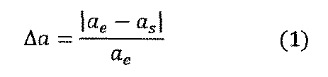
次に、図3(A)および図3(B)を用いて、本発明の一態様である金属酸窒化物膜の作製方法に係るスパッタリング装置について説明する。図3(A)は、スパッタリング装置が有する成膜室41を説明する断面図であり、図3(B)は、スパッタリング装置が有するマグネットユニット54a、およびマグネットユニット54bの平面図である。
エピタキシャル成長の評価は、評価方法によって、薄膜の成膜中または薄膜の成膜後に行うことができる。
広域逆格子空間マッピングについて説明する。

極点測定は、X線源と検出器の位置(角度)を一定に保ったまま、試料をあらゆる方向に回転させることで、回折強度の分布を測定する方法である。極点測定では、検出器として、本明細書では、2次元検出器を用いる。具体的には、検出器detectorを検出角度(2θ)に固定し、試料sampleをθ方向とψ方向に傾けた状態で、面内方向(φ方向)に回転させてあらゆる方向に傾いた格子面を測定する。極点測定で得られる回折強度から、薄膜の結晶性および配向性を評価することができる。なお、極点測定に用いる検出器としては2次元検出器に限られず、0次元検出器でもよい。
XRD法を用いた測定には、Out−of−plane測定およびIn−plane測定がある。Out−of−plane測定は、薄膜の表面に対して平行な結晶面を評価する手法であり、In−plane測定は、薄膜の表面に対して垂直な結晶面を評価する手法である。Out−of−plane測定およびIn−plane測定では、検出器として、0次元検出器を用いても良い。
本実施の形態では、先の実施の形態で示した、エピタキシャル成長した金属酸窒化物膜の用途について説明する。
本実施の形態では、本発明の一態様の発光素子を様々な照明装置に適用する一例について、図7(A)および図7(B)を用いて説明する。本発明の一態様である発光素子を用いることで、発光効率が良好な、信頼性の高い照明装置を作製できる。
本実施の形態では、上記実施の形態で説明した発光素子を用いた表示装置の構成例について、図8(A)乃至図8(C)を用いて説明する。
本実施の形態では、先の実施の形態に示す表示装置を用いた本発明の一態様の電子機器について、図面を参照して説明する。
まず、試料1乃至試料7の作製方法について説明する。

試料1の広域逆格子空間マップを図10(A)に示す。また、シミュレーションで得られた広域逆格子空間マップを図10(B)および図10(C)に示す。図10(B)は、試料1の単結晶の基板に対応する広域逆格子空間マップであり、図10(C)は、試料1の金属酸窒化物膜が有する結晶に対応する広域逆格子空間マップである。
試料2の広域逆格子空間マップを図12(A)に示す。また、シミュレーションで得られた広域逆格子空間マップを図12(B)および図12(C)に示す。図12(B)は、試料2の単結晶の基板に対応する広域逆格子空間マップであり、図12(C)は、試料2の金属酸窒化物膜が有する結晶に対応する広域逆格子空間マップである。
試料3の広域逆格子空間マップを図14(A)に示す。また、シミュレーションで得られた広域逆格子空間マップを図14(B)および図14(C)に示す。図14(B)は、試料3の単結晶の基板に対応する広域逆格子空間マップであり、図14(C)は、試料3の金属酸窒化物膜が有する結晶に対応する広域逆格子空間マップである。
試料4の広域逆格子空間マップを図16(A)に示す。また、シミュレーションで得られた広域逆格子空間マップを図16(B)および図16(C)に示す。図16(B)は、試料4の単結晶の基板に対応する広域逆格子空間マップであり、図16(C)は、試料4の金属酸窒化物膜が有する結晶に対応する広域逆格子空間マップである。
試料5の広域逆格子空間マップを図18(A)に示す。また、シミュレーションで得られた広域逆格子空間マップを図18(B)および図18(C)に示す。図18(B)は、試料5の単結晶の基板に対応する広域逆格子空間マップであり、図18(C)は、試料5の金属酸窒化物膜が有する結晶に対応する広域逆格子空間マップである。
試料6の広域逆格子空間マップを図20(A)に示す。また、シミュレーションで得られた広域逆格子空間マップを図20(B)および図20(C)に示す。図20(B)は、試料6の単結晶の基板に対応する広域逆格子空間マップであり、図20(C)は、試料6の金属酸窒化物膜が有する結晶に対応する広域逆格子空間マップである。
試料7の広域逆格子空間マップを図22(A)に示す。また、シミュレーションで得られた広域逆格子空間マップを図22(B)および図22(C)に示す。図22(B)は、試料7の単結晶の基板に対応する広域逆格子空間マップであり、図22(C)は、試料7の金属酸窒化物膜が有する結晶に対応する広域逆格子空間マップである。
Claims (8)
- 単結晶の基板上に、
窒素ガスを含む気体を導入して、酸化物ターゲットを用いて、スパッタリング法によって、エピタキシャル成長させる金属酸窒化物膜の作製方法であって、
前記酸化物ターゲットは、亜鉛を含み、
前記金属酸窒化物膜の成膜中の前記基板は、80℃以上400℃以下であり、
前記窒素ガスの流量は、前記気体の全流量中の50%以上100%以下である、
金属酸窒化物膜の作製方法。 - 単結晶の基板上に、
窒素ガスを含む気体を導入して、酸化物ターゲットを用いて、スパッタリング法によって、面内配向した膜を成膜する金属酸窒化物膜の作製方法であって、
前記酸化物ターゲットは、亜鉛を含み、
前記金属酸窒化物膜の成膜中の前記基板は、80℃以上400℃以下であり、
前記窒素ガスの流量は、前記気体の全流量中の50%以上100%以下である、
金属酸窒化物膜の作製方法。 - 請求項1または請求項2において、
前記酸化物ターゲットは、インジウムおよびガリウムの少なくとも一を含む、
金属酸窒化物膜の作製方法。 - 請求項1乃至請求項3のいずれか一において、
前記基板は、イットリア安定化ジルコニア(YSZ)基板であり、
前記基板の面方位は(111)である、
金属酸窒化物膜の作製方法。 - 請求項1乃至請求項3のいずれか一において、
前記基板は、A面サファイア基板であり、
前記基板の面方位は(110)である、
金属酸窒化物膜の作製方法。 - 請求項1乃至請求項5のいずれか一において、
前記金属酸窒化物膜の結晶構造は、ウルツ鉱型構造である、
金属酸窒化物膜の作製方法。 - 請求項6において、
前記金属酸窒化物膜に対して、極点測定を行った場合、
極点測定の、前記金属酸窒化物膜の結晶の(101)面に対するφスキャンにて、
6回対称を示す回折ピークが観測される、
金属酸窒化物膜の作製方法。 - 請求項7において、
前記金属酸窒化物膜の広域逆格子空間マップにおいて、第1のスポットと、第2のスポットとが観察され、
前記第1のスポットのピークは、角度2θが30°以上35°以下、かつ、角度ψが0°付近に位置し、
前記第1のスポットの半値幅は、2°未満であり、
前記第2のスポットのピークは、角度2θが33°以上37°以下、かつ、角度ψが61°以上65°以下に位置し、
前記第2のスポットの半値幅が、2°未満である、
金属酸窒化物膜の作製方法。
Priority Applications (9)
| Application Number | Priority Date | Filing Date | Title |
|---|---|---|---|
| CN201980039953.XA CN112335024B (zh) | 2018-07-06 | 2019-06-24 | 金属氧氮化物膜的制造方法 |
| CN202411921844.XA CN119753828A (zh) | 2018-07-06 | 2019-06-24 | 金属氧氮化物膜的制造方法 |
| JP2020528536A JP7296381B2 (ja) | 2018-07-06 | 2019-06-24 | 金属酸窒化物膜の作製方法 |
| US17/257,071 US11728163B2 (en) | 2018-07-06 | 2019-06-24 | Method for manufacturing metal oxynitride film |
| KR1020217003197A KR102943468B1 (ko) | 2018-07-06 | 2019-06-24 | 금속 산화질화물막의 제작 방법 |
| KR1020267008334A KR20260054714A (ko) | 2018-07-06 | 2019-06-24 | 금속 산화질화물막 및 표시 장치 |
| JP2023096241A JP7531660B2 (ja) | 2018-07-06 | 2023-06-12 | 金属酸窒化物膜及び表示装置 |
| US18/232,881 US12315717B2 (en) | 2018-07-06 | 2023-08-11 | Method for manufacturing metal oxynitride film |
| JP2024123599A JP2024163913A (ja) | 2018-07-06 | 2024-07-30 | 金属酸窒化物膜 |
Applications Claiming Priority (2)
| Application Number | Priority Date | Filing Date | Title |
|---|---|---|---|
| JP2018128964 | 2018-07-06 | ||
| JP2018-128964 | 2018-07-06 |
Related Child Applications (2)
| Application Number | Title | Priority Date | Filing Date |
|---|---|---|---|
| US17/257,071 A-371-Of-International US11728163B2 (en) | 2018-07-06 | 2019-06-24 | Method for manufacturing metal oxynitride film |
| US18/232,881 Continuation US12315717B2 (en) | 2018-07-06 | 2023-08-11 | Method for manufacturing metal oxynitride film |
Publications (1)
| Publication Number | Publication Date |
|---|---|
| WO2020008294A1 true WO2020008294A1 (ja) | 2020-01-09 |
Family
ID=69060795
Family Applications (1)
| Application Number | Title | Priority Date | Filing Date |
|---|---|---|---|
| PCT/IB2019/055287 Ceased WO2020008294A1 (ja) | 2018-07-06 | 2019-06-24 | 金属酸窒化物膜の作製方法 |
Country Status (5)
| Country | Link |
|---|---|
| US (2) | US11728163B2 (ja) |
| JP (3) | JP7296381B2 (ja) |
| KR (2) | KR20260054714A (ja) |
| CN (2) | CN112335024B (ja) |
| WO (1) | WO2020008294A1 (ja) |
Cited By (2)
| Publication number | Priority date | Publication date | Assignee | Title |
|---|---|---|---|---|
| JPWO2021161126A1 (ja) * | 2020-02-14 | 2021-08-19 | ||
| WO2025079560A1 (ja) * | 2023-10-11 | 2025-04-17 | 住友化学株式会社 | 金属窒化物、膜、積層体、素子、デバイス、膜の製造方法、磁気トンネル接合素子、及び、磁気デバイス |
Citations (5)
| Publication number | Priority date | Publication date | Assignee | Title |
|---|---|---|---|---|
| JPH07262801A (ja) * | 1994-03-25 | 1995-10-13 | Murata Mfg Co Ltd | 薄膜発光素子及び発光装置 |
| JP2001044500A (ja) * | 1999-07-26 | 2001-02-16 | Agency Of Ind Science & Technol | A面サファイア基板を用いたZnO系化合物半導体発光素子およびその製法 |
| JP2011029238A (ja) * | 2009-07-21 | 2011-02-10 | Fujifilm Corp | 結晶性ホモロガス化合物層を含む積層体の製造方法及び電界効果型トランジスタ |
| WO2017204197A1 (ja) * | 2016-05-26 | 2017-11-30 | 住友化学株式会社 | 金属酸窒化物半導体膜の製造方法および金属酸窒化物半導体膜 |
| JP2017218675A (ja) * | 2016-06-03 | 2017-12-14 | 株式会社半導体エネルギー研究所 | スパッタリングターゲット、酸化物半導体、酸窒化物半導体およびトランジスタ |
Family Cites Families (13)
| Publication number | Priority date | Publication date | Assignee | Title |
|---|---|---|---|---|
| EP1199755A4 (en) | 1999-07-26 | 2004-10-20 | Nat Inst Of Advanced Ind Scien | SEMICONDUCTOR LIGHT EMITTING ELEMENT BASED ON A ZnO COMPOUND |
| US6996147B2 (en) * | 2001-03-30 | 2006-02-07 | The Regents Of The University Of California | Methods of fabricating nanostructures and nanowires and devices fabricated therefrom |
| EP1443130B1 (en) | 2001-11-05 | 2011-09-28 | Japan Science and Technology Agency | Natural superlattice homologous single crystal thin film, method for preparation thereof, and device using said single crystal thin film |
| JP4164562B2 (ja) | 2002-09-11 | 2008-10-15 | 独立行政法人科学技術振興機構 | ホモロガス薄膜を活性層として用いる透明薄膜電界効果型トランジスタ |
| WO2008083073A1 (en) | 2006-12-28 | 2008-07-10 | Saint-Gobain Ceramics & Plastics, Inc. | Sapphire substrates and methods of making same |
| JP5490368B2 (ja) * | 2007-03-26 | 2014-05-14 | 公益財団法人神奈川科学技術アカデミー | エピタキシャル薄膜の形成方法及び半導体基板の製造方法 |
| WO2008133345A1 (en) | 2007-04-25 | 2008-11-06 | Canon Kabushiki Kaisha | Oxynitride semiconductor |
| JP5451280B2 (ja) | 2008-10-09 | 2014-03-26 | キヤノン株式会社 | ウルツ鉱型結晶成長用基板およびその製造方法ならびに半導体装置 |
| JP6095914B2 (ja) * | 2012-07-31 | 2017-03-15 | 三菱重工業株式会社 | エアフィルタ自動清掃機構の制御装置、方法、プログラム、およびそれを備えた空気調和機 |
| JP6217196B2 (ja) | 2013-07-11 | 2017-10-25 | 三菱電機株式会社 | 半導体材料、薄膜トランジスタ、および薄膜トランジスタの製造方法 |
| TWI672804B (zh) * | 2014-05-23 | 2019-09-21 | Semiconductor Energy Laboratory Co., Ltd. | 半導體裝置的製造方法 |
| JP2017216445A (ja) | 2016-05-31 | 2017-12-07 | 出光興産株式会社 | 膜、膜の製造方法、積層体及び半導体デバイス |
| US10347483B2 (en) * | 2017-05-29 | 2019-07-09 | Franck Natali | Rare earth nitride structure or device and fabrication method |
-
2019
- 2019-06-24 KR KR1020267008334A patent/KR20260054714A/ko active Pending
- 2019-06-24 WO PCT/IB2019/055287 patent/WO2020008294A1/ja not_active Ceased
- 2019-06-24 US US17/257,071 patent/US11728163B2/en active Active
- 2019-06-24 JP JP2020528536A patent/JP7296381B2/ja active Active
- 2019-06-24 CN CN201980039953.XA patent/CN112335024B/zh active Active
- 2019-06-24 KR KR1020217003197A patent/KR102943468B1/ko active Active
- 2019-06-24 CN CN202411921844.XA patent/CN119753828A/zh active Pending
-
2023
- 2023-06-12 JP JP2023096241A patent/JP7531660B2/ja active Active
- 2023-08-11 US US18/232,881 patent/US12315717B2/en active Active
-
2024
- 2024-07-30 JP JP2024123599A patent/JP2024163913A/ja active Pending
Patent Citations (5)
| Publication number | Priority date | Publication date | Assignee | Title |
|---|---|---|---|---|
| JPH07262801A (ja) * | 1994-03-25 | 1995-10-13 | Murata Mfg Co Ltd | 薄膜発光素子及び発光装置 |
| JP2001044500A (ja) * | 1999-07-26 | 2001-02-16 | Agency Of Ind Science & Technol | A面サファイア基板を用いたZnO系化合物半導体発光素子およびその製法 |
| JP2011029238A (ja) * | 2009-07-21 | 2011-02-10 | Fujifilm Corp | 結晶性ホモロガス化合物層を含む積層体の製造方法及び電界効果型トランジスタ |
| WO2017204197A1 (ja) * | 2016-05-26 | 2017-11-30 | 住友化学株式会社 | 金属酸窒化物半導体膜の製造方法および金属酸窒化物半導体膜 |
| JP2017218675A (ja) * | 2016-06-03 | 2017-12-14 | 株式会社半導体エネルギー研究所 | スパッタリングターゲット、酸化物半導体、酸窒化物半導体およびトランジスタ |
Non-Patent Citations (1)
| Title |
|---|
| MATSUSHIMA, KOICHI ET AL.: "Epitaxial Growth of ZninON Films with Tunable Band Gap from 1.7 to 3.3 eV on ZnO Templates", JAPANESE JOURNAL OF APPLIED PHYSICS, vol. 52, 20 November 2013 (2013-11-20), pages 11NM06 - 1-11NM06-5, XP055191483 * |
Cited By (3)
| Publication number | Priority date | Publication date | Assignee | Title |
|---|---|---|---|---|
| JPWO2021161126A1 (ja) * | 2020-02-14 | 2021-08-19 | ||
| JP7637078B2 (ja) | 2020-02-14 | 2025-02-27 | 株式会社半導体エネルギー研究所 | 表示装置および電子機器 |
| WO2025079560A1 (ja) * | 2023-10-11 | 2025-04-17 | 住友化学株式会社 | 金属窒化物、膜、積層体、素子、デバイス、膜の製造方法、磁気トンネル接合素子、及び、磁気デバイス |
Also Published As
| Publication number | Publication date |
|---|---|
| JP7531660B2 (ja) | 2024-08-09 |
| US11728163B2 (en) | 2023-08-15 |
| CN112335024A (zh) | 2021-02-05 |
| CN112335024B (zh) | 2025-01-24 |
| KR20260054714A (ko) | 2026-04-22 |
| JP7296381B2 (ja) | 2023-06-22 |
| US12315717B2 (en) | 2025-05-27 |
| US20230402280A1 (en) | 2023-12-14 |
| KR20210027448A (ko) | 2021-03-10 |
| US20210125823A1 (en) | 2021-04-29 |
| JP2024163913A (ja) | 2024-11-22 |
| KR102943468B1 (ko) | 2026-03-25 |
| CN119753828A (zh) | 2025-04-04 |
| JPWO2020008294A1 (ja) | 2021-08-02 |
| JP2023118744A (ja) | 2023-08-25 |
Similar Documents
| Publication | Publication Date | Title |
|---|---|---|
| JP6556396B1 (ja) | 表示装置 | |
| JP2022066258A (ja) | 液晶表示装置 | |
| JP2024163913A (ja) | 金属酸窒化物膜 | |
| US20170309754A1 (en) | Oxide semiconductor film and semiconductor device | |
| JP7820080B2 (ja) | 装置の作製方法および無機発光素子 | |
| TW201801330A (zh) | 半導體裝置、該半導體裝置的製造方法以及包括該半導體裝置的顯示裝置 |
Legal Events
| Date | Code | Title | Description |
|---|---|---|---|
| 121 | Ep: the epo has been informed by wipo that ep was designated in this application |
Ref document number: 19830062 Country of ref document: EP Kind code of ref document: A1 |
|
| ENP | Entry into the national phase |
Ref document number: 2020528536 Country of ref document: JP Kind code of ref document: A |
|
| NENP | Non-entry into the national phase |
Ref country code: DE |
|
| ENP | Entry into the national phase |
Ref document number: 20217003197 Country of ref document: KR Kind code of ref document: A |
|
| 122 | Ep: pct application non-entry in european phase |
Ref document number: 19830062 Country of ref document: EP Kind code of ref document: A1 |
|
| WWG | Wipo information: grant in national office |
Ref document number: 201980039953.X Country of ref document: CN |