WO2020004374A1 - 表示構造体 - Google Patents
表示構造体 Download PDFInfo
- Publication number
- WO2020004374A1 WO2020004374A1 PCT/JP2019/025110 JP2019025110W WO2020004374A1 WO 2020004374 A1 WO2020004374 A1 WO 2020004374A1 JP 2019025110 W JP2019025110 W JP 2019025110W WO 2020004374 A1 WO2020004374 A1 WO 2020004374A1
- Authority
- WO
- WIPO (PCT)
- Prior art keywords
- polarizing member
- light
- pattern
- polarization axis
- polarizing
- Prior art date
- Legal status (The legal status is an assumption and is not a legal conclusion. Google has not performed a legal analysis and makes no representation as to the accuracy of the status listed.)
- Ceased
Links
Images



Classifications
-
- G—PHYSICS
- G02—OPTICS
- G02B—OPTICAL ELEMENTS, SYSTEMS OR APPARATUS
- G02B27/00—Optical systems or apparatus not provided for by any of the groups G02B1/00 - G02B26/00, G02B30/00
- G02B27/28—Optical systems or apparatus not provided for by any of the groups G02B1/00 - G02B26/00, G02B30/00 for polarising
- G02B27/286—Optical systems or apparatus not provided for by any of the groups G02B1/00 - G02B26/00, G02B30/00 for polarising for controlling or changing the state of polarisation, e.g. transforming one polarisation state into another
-
- G—PHYSICS
- G02—OPTICS
- G02B—OPTICAL ELEMENTS, SYSTEMS OR APPARATUS
- G02B27/00—Optical systems or apparatus not provided for by any of the groups G02B1/00 - G02B26/00, G02B30/00
- G02B27/28—Optical systems or apparatus not provided for by any of the groups G02B1/00 - G02B26/00, G02B30/00 for polarising
- G02B27/281—Optical systems or apparatus not provided for by any of the groups G02B1/00 - G02B26/00, G02B30/00 for polarising used for attenuating light intensity, e.g. comprising rotatable polarising elements
-
- G—PHYSICS
- G02—OPTICS
- G02B—OPTICAL ELEMENTS, SYSTEMS OR APPARATUS
- G02B5/00—Optical elements other than lenses
- G02B5/02—Diffusing elements; Afocal elements
- G02B5/0273—Diffusing elements; Afocal elements characterized by the use
- G02B5/0278—Diffusing elements; Afocal elements characterized by the use used in transmission
-
- G—PHYSICS
- G09—EDUCATION; CRYPTOGRAPHY; DISPLAY; ADVERTISING; SEALS
- G09F—DISPLAYING; ADVERTISING; SIGNS; LABELS OR NAME-PLATES; SEALS
- G09F13/00—Illuminated signs; Luminous advertising
- G09F13/04—Signs, boards or panels, illuminated from behind the insignia
-
- H—ELECTRICITY
- H10—SEMICONDUCTOR DEVICES; ELECTRIC SOLID-STATE DEVICES NOT OTHERWISE PROVIDED FOR
- H10H—INORGANIC LIGHT-EMITTING SEMICONDUCTOR DEVICES HAVING POTENTIAL BARRIERS
- H10H20/00—Individual inorganic light-emitting semiconductor devices having potential barriers, e.g. light-emitting diodes [LED]
- H10H20/80—Constructional details
- H10H20/85—Packages
- H10H20/855—Optical field-shaping means, e.g. lenses
-
- H—ELECTRICITY
- H10—SEMICONDUCTOR DEVICES; ELECTRIC SOLID-STATE DEVICES NOT OTHERWISE PROVIDED FOR
- H10H—INORGANIC LIGHT-EMITTING SEMICONDUCTOR DEVICES HAVING POTENTIAL BARRIERS
- H10H20/00—Individual inorganic light-emitting semiconductor devices having potential barriers, e.g. light-emitting diodes [LED]
- H10H20/80—Constructional details
- H10H20/882—Scattering means
Definitions
- the present disclosure relates to a display structure for making a user visually recognize a plurality of patterns.
- Japanese Utility Model Application Publication No. 61-025002 discloses a display switching device using a polarizing member as an example of such a display structure.
- the polarizing member has a polarizing axis extending in a specific direction.
- Light having a polarization component parallel to the polarization axis is allowed to pass through the polarizing member.
- first polarized light Light having a polarization component that is not parallel to the polarization axis is not allowed to pass.
- second polarized light such light is referred to as first polarized light.
- a polarizing member that does not allow passage by absorbing the second polarized light is called an absorption-type polarizing member.
- the absorption-type polarizing member can be formed by, for example, stretching a PVA (polyvinyl alcohol) film substrate impregnated with an iodine compound in a specific direction and performing a crosslinking treatment.
- a plurality of polarizing plates having different polarization axes are arranged on the path of light emitted from the light source. Different transparent patterns are formed on the plurality of polarizing plates.
- a display structure is formed by a plurality of polarizing plates each having a transparent pattern formed thereon.
- transparent in the following description means a characteristic that allows passage of both the first polarized light and the second polarized light.
- pattern in the following description is meant to include figures, characters, symbols, marks, pictures, and the like.
- the second polarized light is formed for a specific polarizing plate by switching the polarization direction of the incident light.
- the incident light passes only through the area where the pattern is formed on the specific polarizing plate.
- the pattern is visually recognized by the user.
- the “specific polarizing plate” can be changed, and the pattern used for display to the user can be switched.
- the display structure since a plurality of polarizing plates are arranged on the path of the light emitted from the light source, there are portions where the plurality of patterns overlap each other when viewed from the direction along the path.
- the amount of light passing therethrough may be different between a portion where a plurality of patterns overlap each other and a portion where the patterns do not overlap. Thereby, desired visibility may not be obtained for each of the plurality of patterns visually recognized by the user through the display structure.
- a first polarized light having a first polarization axis and allowing light having a polarization component parallel to the first polarization axis to pass therethrough, and not allowing light having a polarization component not parallel to the first polarization axis to pass therethrough.
- Components A second polarized light having a second polarization axis and allowing light having a polarization component parallel to the second polarization axis to pass therethrough, and not allowing light having a polarization component non-parallel to the second polarization axis to pass therethrough.
- the first polarizing member and the second polarizing member are arranged such that the direction of the first polarization axis and the direction of the second polarization axis are non-parallel,
- the first polarizing member has a portion in which a first pattern that allows light to pass regardless of the direction of the polarized light component is formed,
- the second polarizing member has a portion where a second pattern that allows light to pass regardless of the direction of the polarized light component is formed,
- the optical resin is filled in at least a portion where the first pattern is formed and a portion where the second pattern is formed.
- a portion where the edge of the pattern of one polarizing member overlaps the pattern of the other polarizing member when viewed from the arrangement direction of the first polarizing member and the second polarizing member may occur.
- the optical resin is filled into the portion where the first pattern is formed and the portion where the second pattern is formed, so that the optical resin is arranged at the position when viewed from the arrangement direction of the first polarizing member and the second polarizing member.
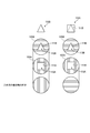
- FIG. 2 illustrates a configuration of a display device according to a first embodiment. It is a figure explaining the operation principle of the above-mentioned display. 2 illustrates a partial configuration of the above display device. 9 illustrates a configuration of a display device according to a second embodiment.
- FIG. 1 illustrates a configuration of a display device 1000 according to the first embodiment.
- the display device 1000 is driven by electric power supplied from an internal power supply such as a battery or electric power supplied from an external power supply such as a commercial power supply.
- the display device 1000 includes the first polarizing member 100A and the second polarizing member 100B.
- the first polarizing member 100A and the second polarizing member 100B form a display structure.
- the first polarizing member 100A includes a base material having a first polarizing axis.
- the first polarizing member 100A allows passage of light having a polarization axis parallel to the first polarization axis.
- the first polarizing member 100A does not allow passage of light having a polarization axis that is not parallel to the first polarization axis.
- the first polarizing member 100A may be an absorption polarizing member.
- the first polarizing member 100A transmits light having a polarization axis parallel to the first polarization axis and absorbs light having a polarization axis non-parallel to the first polarization axis.
- a first pattern 110A having an arbitrary shape is formed on the first polarizing member 100A.
- the first pattern 110A is formed by removing a part of the base material by punching or laser processing. The processing is desirably performed so that burrs do not occur at the edges of the pattern. Light incident on the first pattern 110A is allowed to pass regardless of the polarization direction.
- the first polarizing member 100A may be a reflective polarizing member.
- the first polarizing member 100A transmits light having a polarization axis parallel to the first polarization axis and reflects light having a polarization axis non-parallel to the first polarization axis.
- the reflective polarizing member can be formed by depositing a metal on a film substrate having a nanogrid structure.
- the film substrate may be formed of TAC (triacetylcellulose), COP (cyclo-olefin polymer), or the like. Examples of metals to be deposited include aluminum, silver, chromium, and the like.
- the first pattern 110A can be formed by removing a portion where a metal is deposited by punching or laser processing.
- the second polarizing member 100B includes a substrate having a second polarizing axis.
- the second polarizing member 100B allows passage of light having a polarization axis parallel to the second polarization axis.
- the second polarizing member 100B does not allow passage of light having a polarization axis that is not parallel to the second polarization axis.
- the second polarizing member 100B may be an absorption polarizing member.
- the second polarizing member 100B transmits light having a polarization axis parallel to the second polarization axis and absorbs light having a polarization axis non-parallel to the second polarization axis.
- a second pattern 110B having an arbitrary shape is formed on the second polarizing member 100B.
- the second pattern 110B is formed by removing a part of the base material by punching or laser processing. The processing is desirably performed so that burrs do not occur at the edges of the pattern. Light incident on the second pattern 110B is allowed to pass regardless of its polarization direction.
- the second polarizing member 100B can be a reflective polarizing member like the first polarizing member 100A.
- the second polarizing member 100B transmits light having a polarization axis parallel to the second polarization axis, and reflects light having a polarization axis non-parallel to the second polarization axis.
- the above-described second pattern 110B can be formed by removing a portion where a metal is deposited by punching or laser processing.
- the first polarizing member 100A and the second polarizing member 100B are arranged so as to be arranged along the traveling direction of incident light.
- the first polarizing member 100A and the second polarizing member 100B are arranged such that the direction of the first polarizing axis and the direction of the second polarizing axis are non-parallel.
- the polarized light allowed to pass through the first polarizing member 100A is And the second polarizing member 100B is not allowed to pass. Similarly, polarized light that is allowed to pass through the second polarizing member 100B is not allowed to pass through the first polarizing member 100A.
- (1) Display of the second pattern 110B By setting the polarization axis of the light incident on the display structure to have a component parallel to the first polarization axis of the first polarizing member 100A, the incident light becomes the first light. The light passes through the polarizing member 100A. Since the polarization axis of the polarized light that has passed through the first polarizing member 100A crosses the second polarizing axis of the second polarizing member 100B, the polarized light does not pass through the second polarizing member 100B. However, the second pattern 110B formed on the second polarizing member 100B allows the transmission of the polarized light.
- the light that has passed through the second pattern 110B can be visually recognized by the user.
- the shape of the second pattern 110B can be provided for display to the user.
- the light that has passed through the first pattern 110A can be visually recognized by the user.
- the shape of the first pattern 110A can be provided for display to the user.
- a pattern provided for display to a user can be switched by the display structure including a plurality of polarizing members each having a pattern formed thereon.
- the edge 111A of the first pattern 110A overlaps with the second pattern 110B when viewed from the direction of the incident light.
- the edge 111B of the second pattern 110B overlaps with the first pattern 110A when viewed from the arrangement direction of the first polarizing member 100A and the second polarizing member 100B.
- uneven brightness of the pattern may be visually recognized.
- the first optical resin 120A is filled in the first polarizing member 100A at the portion where the first pattern 110A is formed.
- a portion of the second polarizing member 100B where the second pattern 110B is formed is filled with the second optical resin 120B.
- Each of the first optical resin 120A and the second optical resin 120B has a property of maintaining the polarization state of light passing therethrough. Since the polarization state is prevented from being destroyed due to the shift in the phase difference, the visibility of each pattern is prevented from lowering.
- the optical resin having the above-described characteristics causes the edge of the pattern of one polarizing member to overlap the pattern of the other polarizing member when viewed from the arrangement direction of the plurality of polarizing members. It is placed in the place where.
- the inventor has found that such a configuration suppresses luminance unevenness of a pattern that can be visually recognized at the location. Therefore, desired visibility can be obtained for each of the plurality of patterns visually recognized by the user through the display structure.
- OCR Optically Clear Resin
- Silicon-based OCR or acrylic-based OCR can be used.
- OCR is useful in that it can also be used as an optical bonding agent.
- the OCR is liquid in an initial state, but is cured by irradiating light having a predetermined wavelength such as ultraviolet light.
- a predetermined wavelength such as ultraviolet light.
- optical resins that can be used as optical bonding agents are not limited to photocurable resins. Thermosetting resins may also be used.
- the display device 1000 may include a third polarizing member 200A.
- the third polarizing member 200A includes a substrate having a third polarizing axis.
- the direction of the third polarization axis is parallel to the direction of the first polarization axis of the first polarizing member 100A. Therefore, light passing through the third polarizing member 200A can pass through the base material of the first polarizing member 100A, but cannot pass through the base material of the second polarizing member 100B.
- the display device 1000 may include a fourth polarizing member 200B.
- the fourth polarizing member 200B includes a substrate having a fourth polarizing axis.
- the direction of the fourth polarization axis is parallel to the direction of the second polarization axis of the second polarizing member 100B. Therefore, light passing through the fourth polarizing member 200B can pass through the base material of the second polarizing member 100B, but cannot pass through the base material of the first polarizing member 100A.
- Each of the third polarizing member 200A and the fourth polarizing member 200B may be an absorption polarizing member or a reflection polarizing member.
- any of the display states (1) to (3) described above can be selectively realized.
- the arrangement of the third polarizing member 200A and the fourth polarizing member 200B can be appropriately determined as long as the light can pass before entering the display structure.
- the display device 1000 can include a first light source LS1 and a second light source LS2.
- the first light source LS1 is arranged so that the emitted light passes through the third polarizing member 200A.
- the second light source LS2 is arranged so that the emitted light passes through the fourth polarizing member 200B.
- Each of the first light source LS1 and the second light source LS2 can be configured by at least one semiconductor light emitting element that emits light of at least one color.
- the semiconductor light emitting device include a light emitting diode (LED), a laser diode (LD), an organic EL device, and the like.
- Each of the first light source LS1 and the second light source LS2 may be a lamp light source such as a halogen lamp.
- the turning on / off of each of the first light source LS1 and the second light source LS2 can be controlled by a processor (not shown) included in the display device 1000.
- the display device 1000 can include a mechanism for changing the position of a single light source between a first position and a second position. In this case, light emitted from the single light source located at the first position passes through the third polarizing member 200A, and light emitted from the single light source located at the second position passes through the fourth polarizing member 200B. pass.
- the display device 1000 may include a mechanism for arranging at least one of the third polarizing member 200A and the fourth polarizing member 200B on the path of light emitted from a single light source.
- the light may be supplied from outside the display device 1000.
- FIG. 4 illustrates a configuration of a display structure 2000 according to the second embodiment. Elements that are substantially the same as the components in the display device 1000 according to the first embodiment are given the same reference numerals, and a repeated description is omitted.
- the display structure 2000 includes the first polarizing member 100A, the second polarizing member 100B, and the optical resin 120.
- the optical resin 120 has a characteristic that can be used as an optical bonding agent, in addition to a characteristic of maintaining the polarization state of light passing therethrough.
- An example of such an optical resin is OCR.
- the optical resin 120 is filled in a portion of the first polarizing member 100A where the first pattern 110A is formed, and in a portion of the second polarizing member 100B where the second pattern 110B is formed. Further, the optical resin 120 is also filled between the first polarizing member 100A and the second polarizing member 100B in the arrangement direction. The first polarizing member 100A and the second polarizing member 100B are joined by an integrated optical resin 120.
- the defoamed liquid OCR is filled in a portion of the first polarizing member 100A where the first pattern 110A is formed and a portion of the second polarizing member 100B where the second pattern 110B is formed. Is done. Further, the defoamed liquid OCR is also filled between the first polarizing member 100A and the second polarizing member 100B in the arrangement direction. Subsequently, by performing a curing process, the base of the first polarizing member 100A and the optical resin 120 are bonded, and the base of the second polarizing member 100B and the optical resin 120 are bonded. As a result, the first polarizing member 100A and the second polarizing member 100B are also combined.
- the edge of the pattern of one polarizing member overlaps the pattern of the other polarizing member. It has a place where it is.
- the optical resin 120 is disposed so as to overlap with the corresponding portion when viewed from the arrangement direction of the first polarizing member 100A and the second polarizing member 100B. Therefore, the luminance unevenness of the pattern that can be visually recognized at the location is suppressed.
- first polarizing member 100A and the second polarizing member 100B are joined by the integral optical resin 120, the warping and shrinkage of each polarizing member that may occur in a high-humidity environment or the like are prevented, and the display structure 2000 Deformation can be suppressed.
- the display structure 2000 may include the diffusion member 300.
- the diffusion member 300 optically diffuses the light that has passed through the first polarizing member 100A and the second polarizing member 100B.
- the optical diffusion properties may be isotropic or anisotropic.
- the optical resin 120 may be filled between the second polarizing member 100B and the diffusion member 300. That is, the first polarizing member 100 ⁇ / b> A, the second polarizing member 100 ⁇ / b> B, and the diffusion member 300 can be combined by the integrated optical resin 120. The effect is as described above.
- the display structure 2000 may include a light attenuating member 400.
- the light attenuating member 400 attenuates the intensity of light that has passed through the first polarizing member 100A and the second polarizing member 100B.
- a smoke material or the like formed by a gray or black visible light cut filter can be used as the light attenuating member 400.
- the shape of the light attenuating member 400 can be appropriately determined.
- the diffusion member 300 may be omitted.
- the optical resin 120 may be filled between the second polarizing member 100B and the light attenuating member 400. That is, the first polarizing member 100A, the second polarizing member 100B, and the light attenuating member 400 can be combined by the integrated optical resin 120. The effect is as described above.
- the third polarizing member 200A, the fourth polarizing member 200B, and at least one light source described with reference to the display device 1000 according to the first embodiment can be combined with the display structure 2000 according to the second embodiment.
Landscapes
- Physics & Mathematics (AREA)
- General Physics & Mathematics (AREA)
- Optics & Photonics (AREA)
- Engineering & Computer Science (AREA)
- Theoretical Computer Science (AREA)
- Polarising Elements (AREA)
- Optical Elements Other Than Lenses (AREA)
- Illuminated Signs And Luminous Advertising (AREA)
Abstract
第一偏光部材(100A)は、第一偏光軸を有するとともに、当該第一偏光軸に平行な偏光成分を有する光の通過を許容し、かつ当該第一偏光軸に非平行な偏光成分を有する光の通過を許容しない。第二偏光部材(100B)は、第二偏光軸を有するとともに、当該第二偏光軸に平行な偏光成分を有する光の通過を許容し、かつ当該第二偏光軸に非平行な偏光成分を有する光の通過を許容しない。第一偏光部材(100A)と第二偏光部材(100B)は、第一偏光軸の向きと第二偏光軸の向きが非平行となるように配列されている。第一偏光部材(100A)は、偏光成分の方向に依らず光の通過を許容する第一パターン(110A)が形成された部分を有している。第二偏光部材(100B)は、偏光成分の方向に依らず光の通過を許容する第二パターン(110B)が形成された部分を有している。第一パターン(110A)が形成された部分と第二パターン(110B)が形成された部分に光学樹脂(120A、120B)が充填されている。
Description
本開示は、複数のパターンをユーザに視認させるための表示構造体に関連する。
日本国実用新案出願公告昭61-025002号公報は、そのような表示構造体の一例として、偏光部材を用いた表示切替装置を開示している。
偏光部材は、特定の向きに延びる偏光軸を有している。偏光軸に平行な偏光成分を有する光は、偏光部材の通過を許容される。以降の説明においては、このような光を第一偏光と称する。偏光軸と平行でない偏光成分を有する光は、通過を許容されない。以降の説明においては、このような光を第二偏光と称する。
第二偏光を吸収することによって通過を許容しない偏光部材は、吸収型偏光部材と称される。吸収型偏光部材は、例えば、ヨウ素化合物を浸透させたPVA(polyvinyl alcohol)フィルム基材を特定の方向へ延伸し、架橋処理を施すことによって形成されうる。
上記の表示切替装置においては、光源から出射された光の進路上に偏光軸の向きが相違する複数の偏光板が配置されている。当該複数の偏光板には、相違する透明なパターンが形成されている。各々に透明なパターンが形成された複数の偏光板により、表示構造体が形成されている。以降の説明における「透明」という語は、第一偏光と第二偏光の双方について通過を許容する特性を意味する。以降の説明における「パターン」という語は、図形、文字、シンボル、マーク、絵柄などを含む意味である。
吸収型偏光部材に上記のようなパターンを形成する手法としては、当該パターンの形状に対応する基材の一部を除去することが知られている。
上記の表示切替装置においては、入射させる光の偏光方向を切り替えることにより、特定の偏光板について第二偏光を形成している。入射光は、当該特定の偏光板においてパターンが形成された領域のみを通過する。結果として、当該パターンがユーザに視認される。入射させる光の偏光方向を変更することにより、「特定の偏光板」を変更でき、ユーザへの表示に供されるパターンが切り替えられる。
上記の表示構造体においては、光源から出射された光の進路上に複数の偏光板が配置されているので、当該進路に沿う方向から見ると複数のパターン同士が重なっている部分が存在する。複数のパターン同士が重なっている部分と重なっていない部分との間では、通過する光量が相違しうる。これにより、表示構造体を通じてユーザに視認される複数のパターンの各々について所望の視認性が得られない場合がある。
したがって、表示構造体を通じてユーザに視認される複数のパターンの各々について所望の視認性が得られるようにすることが求められている。
上記の要求に応えるための一態様は、表示構造体であって、
第一偏光軸を有するとともに、当該第一偏光軸に平行な偏光成分を有する光の通過を許容し、かつ当該第一偏光軸に非平行な偏光成分を有する光の通過を許容しない第一偏光部材と、
第二偏光軸を有するとともに、当該第二偏光軸に平行な偏光成分を有する光の通過を許容し、かつ当該第二偏光軸に非平行な偏光成分を有する光の通過を許容しない第二偏光部材と、
光学樹脂と、
を備えており、
前記第一偏光部材と前記第二偏光部材は、前記第一偏光軸の向きと前記第二偏光軸の向きが非平行となるように配列されており、
前記第一偏光部材は、偏光成分の方向に依らず光の通過を許容する第一パターンが形成された部分を有しており、
前記第二偏光部材は、偏光成分の方向に依らず光の通過を許容する第二パターンが形成された部分を有しており、
前記光学樹脂は、少なくとも前記第一パターンが形成された部分と前記第二パターンが形成された部分に充填されている。
第一偏光軸を有するとともに、当該第一偏光軸に平行な偏光成分を有する光の通過を許容し、かつ当該第一偏光軸に非平行な偏光成分を有する光の通過を許容しない第一偏光部材と、
第二偏光軸を有するとともに、当該第二偏光軸に平行な偏光成分を有する光の通過を許容し、かつ当該第二偏光軸に非平行な偏光成分を有する光の通過を許容しない第二偏光部材と、
光学樹脂と、
を備えており、
前記第一偏光部材と前記第二偏光部材は、前記第一偏光軸の向きと前記第二偏光軸の向きが非平行となるように配列されており、
前記第一偏光部材は、偏光成分の方向に依らず光の通過を許容する第一パターンが形成された部分を有しており、
前記第二偏光部材は、偏光成分の方向に依らず光の通過を許容する第二パターンが形成された部分を有しており、
前記光学樹脂は、少なくとも前記第一パターンが形成された部分と前記第二パターンが形成された部分に充填されている。
上記のような構成を有する表示構造体においては、第一偏光部材と第二偏光部材の配列方向から見て一方の偏光部材のパターンの縁が他方の偏光部材のパターンに重なる箇所が生じうる。当該箇所においては、パターンの輝度ムラが視認される可能性がある。第一パターンが形成された部分と第二パターンが形成された部分に光学樹脂が充填されることにより、第一偏光部材と第二偏光部材の配列方向から見て当該箇所に光学樹脂が配置される。発明者は、このような構成によりパターンの輝度ムラが抑制されることを見出した。したがって、表示構造体を通じてユーザに視認される複数のパターンの各々について所望の視認性が得られる。
添付の図面を参照しつつ、実施形態の例について以下詳細に説明する。以下の説明に用いる各図面では、各部材を認識可能な大きさとするために縮尺を適宜変更している。
図1は、第一実施形態に係る表示装置1000の構成を例示している。表示装置1000は、バッテリなどの内部電源から供給される電力、あるいは商用電源などの外部電源から供給される電力によって駆動される。
表示装置1000は、第一偏光部材100Aと第二偏光部材100Bを備えている。第一偏光部材100Aと第二偏光部材100Bは、表示構造体を形成している。
第一偏光部材100Aは、第一偏光軸を有する基材を備えている。第一偏光部材100Aは、第一偏光軸に平行な偏光軸を有する光の通過を許容する。第一偏光部材100Aは、第一偏光軸と非平行な偏光軸を有する光の通過を許容しない。
第一偏光部材100Aは、吸収型偏光部材でありうる。この場合、第一偏光部材100Aは、第一偏光軸に平行な偏光軸を有する光を通過させ、第一偏光軸と非平行な偏光軸を有する光を吸収する。
第一偏光部材100Aには、任意の形状を有する第一パターン110Aが形成されている。第一偏光部材100Aが吸収型偏光部材である場合、第一パターン110Aは、基材の一部が穴抜き加工やレーザ加工により除去されることによって形成される。加工は、パターンの縁にバリが生じないように行なわれることが望ましい。第一パターン110Aに入射した光は、その偏光方向に依らず、通過を許容される。
第一偏光部材100Aは、反射型偏光部材でありうる。この場合、第一偏光部材100Aは、第一偏光軸に平行な偏光軸を有する光を通過させ、第一偏光軸と非平行な偏光軸を有する光を反射する。反射型偏光部材は、ナノグリッド構造を有するフィルム基材上に金属が蒸着されることにより形成されうる。フィルム基材は、TAC(triacetylcellulose)、COP(cyclo-olefin polymer)などによって形成されうる。蒸着される金属の例としては、アルミニウム、銀、クロムなどが挙げられる。
第一偏光部材100Aが反射型偏光部材である場合、上記の第一パターン110Aは、金属が蒸着された部分が穴抜き加工やレーザ加工により除去されることによって形成されうる。
第二偏光部材100Bは、第二偏光軸を有する基材を備えている。第二偏光部材100Bは、第二偏光軸に平行な偏光軸を有する光の通過を許容する。第二偏光部材100Bは、第二偏光軸と非平行な偏光軸を有する光の通過を許容しない。
第二偏光部材100Bは、吸収型偏光部材でありうる。この場合、第二偏光部材100Bは、第二偏光軸に平行な偏光軸を有する光を通過させ、第二偏光軸と非平行な偏光軸を有する光を吸収する。
第二偏光部材100Bには、任意の形状を有する第二パターン110Bが形成されている。第二偏光部材100Bが吸収型偏光部材である場合、第二パターン110Bは、基材の一部が穴抜き加工やレーザ加工により除去されることによって形成される。加工は、パターンの縁にバリが生じないように行なわれることが望ましい。第二パターン110Bに入射した光は、その偏光方向に依らず、通過を許容される。
第二偏光部材100Bは、第一偏光部材100Aと同様に反射型偏光部材でありうる。この場合、第二偏光部材100Bは、第二偏光軸に平行な偏光軸を有する光を通過させ、第二偏光軸と非平行な偏光軸を有する光を反射する。第二偏光部材100Bが反射型偏光部材である場合、上記の第二パターン110Bは、金属が蒸着された部分が穴抜き加工やレーザ加工により除去されることによって形成されうる。
第一偏光部材100Aと第二偏光部材100Bは、入射光の進行方向に沿って並ぶように配置されている。第一偏光部材100Aと第二偏光部材100Bは、第一偏光軸の向きと第二偏光軸の向きが非平行となるように配置されている。
第一偏光軸と第二偏光軸が上記のような関係となるように第一偏光部材100Aと第二偏光部材100Bが配置されることにより、第一偏光部材100Aの通過を許容される偏光は、第二偏光部材100Bの通過を許容されない。同様に、第二偏光部材100Bの通過を許容される偏光は、第一偏光部材100Aの通過を許容されない。
すなわち、第一偏光部材100Aと第二偏光部材100Bにより形成される表示構造体に入射する光の偏光状態を適宜に設定することにより、以下に列挙される三通りの表示状態を実現できる。図2を参照しつつ、その原理について説明する。
(1)第二パターン110Bの表示
表示構造体に入射する光の偏光軸が第一偏光部材100Aの第一偏光軸に平行な成分を有するように設定することにより、当該入射光は、第一偏光部材100Aを通過する。第一偏光部材100Aを通過した偏光の偏光軸は第二偏光部材100Bの第二偏光軸と交差しているので、当該偏光は、第二偏光部材100Bを通過しない。しかしながら、第二偏光部材100Bに形成された第二パターン110Bは、当該偏光の通過を許容する。
表示構造体に入射する光の偏光軸が第一偏光部材100Aの第一偏光軸に平行な成分を有するように設定することにより、当該入射光は、第一偏光部材100Aを通過する。第一偏光部材100Aを通過した偏光の偏光軸は第二偏光部材100Bの第二偏光軸と交差しているので、当該偏光は、第二偏光部材100Bを通過しない。しかしながら、第二偏光部材100Bに形成された第二パターン110Bは、当該偏光の通過を許容する。
したがって、第二パターン110Bを通過した光が、ユーザに視認されうる。換言すると、第二パターン110Bの形状が、当該ユーザへの表示に供されうる。
(2)第一パターン110Aの表示
表示構造体に入射する光の偏光軸が第二偏光部材100Bの第二偏光軸に平行な成分を有するように設定することにより、当該入射光は、第一偏光部材100Aを通過しない。しかしながら、第一偏光部材100Aに形成された第一パターン110Aは、当該偏光の通過を許容する。また、第一パターン110Aを通過した偏光の偏光軸は第二偏光部材100Bの第二偏光軸と平行であるので、当該偏光は、第二偏光部材100Bを通過する。
表示構造体に入射する光の偏光軸が第二偏光部材100Bの第二偏光軸に平行な成分を有するように設定することにより、当該入射光は、第一偏光部材100Aを通過しない。しかしながら、第一偏光部材100Aに形成された第一パターン110Aは、当該偏光の通過を許容する。また、第一パターン110Aを通過した偏光の偏光軸は第二偏光部材100Bの第二偏光軸と平行であるので、当該偏光は、第二偏光部材100Bを通過する。
したがって、第一パターン110Aを通過した光が、ユーザに視認されうる。換言すると、第一パターン110Aの形状が、当該ユーザへの表示に供されうる。
(3)第一パターン110Aと第二パターン110Bの表示
表示構造体に入射する光の偏光軸が第一偏光部材100Aの第一偏光軸に平行な成分と第二偏光部材100Bの第二偏光軸に平行な成分を有するように設定することにより、上記(1)にて説明したように第二パターン110Bが表示に供されるとともに、上記(2)にて説明したように第一パターン110Aが表示に供される。
表示構造体に入射する光の偏光軸が第一偏光部材100Aの第一偏光軸に平行な成分と第二偏光部材100Bの第二偏光軸に平行な成分を有するように設定することにより、上記(1)にて説明したように第二パターン110Bが表示に供されるとともに、上記(2)にて説明したように第一パターン110Aが表示に供される。
このようにして、各々にパターンが形成されている複数の偏光部材を備えた表示構造体により、ユーザへの表示に供されるパターンを切り替えることができる。
図1に例示される構成においては、入射光の方向から見て第一パターン110Aの縁111Aが第二パターン110Bと重なっている。同様に、第一偏光部材100Aと第二偏光部材100Bの配列方向から見て第二パターン110Bの縁111Bが第一パターン110Aと重なっている。このように複数の偏光部材の配列方向から見て一方の偏光部材のパターンの縁が他方の偏光部材のパターンに重なっている箇所においては、パターンの輝度ムラが視認される場合がある。
例えば、図2に例示される第一パターン110Aが視認される場合において、第二パターン110Bの縁111Bの形状に対応する輝度ムラが生じうる。
図3に例示されるように、本実施形態においては、第一偏光部材100Aにおける第一パターン110Aが形成されている部分に、第一光学樹脂120Aが充填されている。同様に、第二偏光部材100Bにおける第二パターン110Bが形成されている部分に、第二光学樹脂120Bが充填されている。
第一光学樹脂120Aと第二光学樹脂120Bの各々は、通過する光の偏光状態を保持する特性を有している。位相差のずれによって偏光状態が崩れることが防止されるので、各パターンの視認性の低下が防止される。
これにより、図1に例示されるように、上記のような特性を有する光学樹脂が、複数の偏光部材の配列方向から見て一方の偏光部材のパターンの縁が他方の偏光部材のパターンに重なっている箇所に配置される。発明者は、当該箇所において視認されうるパターンの輝度ムラが、このような構成によって抑制されることを見出した。したがって、表示構造体を通じてユーザに視認される複数のパターンの各々について所望の視認性が得られる。
このような特性を有する光学樹脂の一例として、OCR(Optically Clear Resin)が使用されうる。シリコン系OCRやアクリル系OCRが使用されうる。
OCRは、オプティカルボンディング剤としても使用できる点において有用である。OCRは、初期状態においては液状であるが、紫外線などの所定の波長を有する光を照射することによって硬化する。脱泡された液状のOCRを用いることにより、偏光部材においてパターンが形成されている部分が隙間なく充填されるとともに、硬化された光学樹脂を周囲の基材と強固に結合させることができる。
オプティカルボンディング剤として使用できる光学樹脂は、光硬化性樹脂に限られない。熱硬化性樹脂も用いてもよい。
図1に例示されるように、表示装置1000は、第三偏光部材200Aを備えうる。第三偏光部材200Aは、第三偏光軸を有する基材を備えている。第三偏光軸の向きは、第一偏光部材100Aの第一偏光軸の向きと平行である。したがって、第三偏光部材200Aを通過する光は、第一偏光部材100Aの基材を通過できるが、第二偏光部材100Bの基材を通過できない。
図1に例示されるように、表示装置1000は、第四偏光部材200Bを備えうる。第四偏光部材200Bは、第四偏光軸を有する基材を備えている。第四偏光軸の向きは、第二偏光部材100Bの第二偏光軸の向きと平行である。したがって、第四偏光部材200Bを通過する光は、第二偏光部材100Bの基材を通過できるが、第一偏光部材100Aの基材を通過できない。
第三偏光部材200Aと第四偏光部材200Bの各々は、吸収型偏光部材であってもよいし、反射型偏光部材であってもよい。
このように構成された第三偏光部材200Aと第四偏光部材200Bの少なくとも一方を通過した光を、第一偏光部材100Aと第二偏光部材100Bにより形成される表示構造体に入射させることにより、前述した(1)から(3)の表示状態のいずれかを選択的に実現できる。表示構造体に入射する前に光を通過させることができれば、第三偏光部材200Aと第四偏光部材200Bの配置は、適宜に定められうる。
図1に例示されるように、表示装置1000は、第一光源LS1と第二光源LS2を備えうる。第一光源LS1は、その出射光が第三偏光部材200Aを通過するように配置される。第二光源LS2は、その出射光が第四偏光部材200Bを通過するように配置される。
第一光源LS1と第二光源LS2の各々は、少なくとも一色の光を出射する少なくとも一つの半導体発光素子により構成されうる。半導体発光素子の例としては、発光ダイオード(LED)、レーザダイオード(LD)、有機EL素子などが挙げられる。第一光源LS1と第二光源LS2の各々は、ハロゲンランプなどのランプ光源であってもよい。第一光源LS1と第二光源LS2の各々の点消灯は、表示装置1000が備えている不図示のプロセッサにより制御されうる。
このような構成によれば、第一光源LS1と第二光源LS2の各々の発光状態を制御することにより、前述した(1)から(3)の表示状態のいずれかを選択的に実現できる。
表示構造体への入射に先立って第三偏光部材200Aと第四偏光部材200Bの少なくとも一方に光を通過させることができれば、当該光を出射する光源は、複数であることを要しない。例えば、表示装置1000は、単一の光源の位置を第一位置と第二位置との間で変更する機構を備えうる。この場合、第一位置に配置された単一光源から出射された光が第三偏光部材200Aを通過し、第二位置に配置された単一光源から出射されて光が第四偏光部材200Bを通過する。あるいは、表示装置1000は、第三偏光部材200Aと第四偏光部材200Bの少なくとも一方を、単一の光源から出射された光の進路上に配置する機構を備えうる。
表示構造体への入射に先立って第三偏光部材200Aと第四偏光部材200Bの少なくとも一方に光を通過させることができれば、当該光は、表示装置1000の外部から供給されてもよい。
図4は、第二実施形態に係る表示構造体2000の構成を例示している。第一実施形態に係る表示装置1000における構成要素と実質的に同一の要素については、同一の参照符号を付与し、繰り返しとなる説明は省略する。
表示構造体2000は、第一偏光部材100A、第二偏光部材100B、および光学樹脂120を備えている。光学樹脂120は、通過する光の偏光状態を維持する特性に加え、オプティカルボンディング剤として使用されうる特性を有している。このような光学樹脂の例としては、OCRが挙げられる。
光学樹脂120は、第一偏光部材100Aにおける第一パターン110Aが形成されている部分、および第二偏光部材100Bにおける第二パターン110Bが形成されている部分に充填されている。さらに、光学樹脂120は、第一偏光部材100Aと第二偏光部材100Bの配列方向における両者の間にも充填されている。第一偏光部材100Aと第二偏光部材100Bは、一体の光学樹脂120によって結合されている。
具体的には、脱泡された液状のOCRが、第一偏光部材100Aにおける第一パターン110Aが形成されている部分、および第二偏光部材100Bにおける第二パターン110Bが形成されている部分に充填される。さらに、脱泡された液状のOCRが、第一偏光部材100Aと第二偏光部材100Bの配列方向における両者の間にも充填される。続いて硬化処理がなされることにより、第一偏光部材100Aの基材と光学樹脂120の結合、第二偏光部材100Bの基材と光学樹脂120の結合がなされる。結果として、第一偏光部材100Aと第二偏光部材100Bの結合もなされる。
図4に例示されるように、表示構造体2000は、第一偏光部材100Aと第二偏光部材100Bの配列方向から見て一方の偏光部材のパターンの縁が他方の偏光部材のパターンと重なっている箇所を有している。他方、光学樹脂120は、第一偏光部材100Aと第二偏光部材100Bの配列方向から見て当該箇所に重なるように配置されている。したがって、当該箇所において視認されうるパターンの輝度ムラが抑制される。さらに、第一偏光部材100Aと第二偏光部材100Bが一体の光学樹脂120によって結合されているので、高湿環境下などにおいて生じうる各偏光部材の反りや収縮が防止され、表示構造体2000の変形を抑制できる。
図4に例示されるように、表示構造体2000は、拡散部材300を備えうる。拡散部材300は、第一偏光部材100Aと第二偏光部材100Bを通過した光を、光学的に拡散させる。光学的拡散特性は、等方性であっても異方性であってもよい。
このような構成によれば、第一偏光部材100Aと第二偏光部材100Bを通過した光が拡散に供されるので、輝度ムラが視認される可能性をさらに低減できる。
光学樹脂120は、第二偏光部材100Bと拡散部材300の間に充填されてもよい。すなわち、第一偏光部材100A、第二偏光部材100B、および拡散部材300は、一体の光学樹脂120によって結合されうる。その効果は前述の通りである。
図4に例示されるように、表示構造体2000は、光減衰部材400を備えうる。光減衰部材400は、第一偏光部材100Aと第二偏光部材100Bを通過した光の強度を減衰させる。光減衰部材400としては、灰色系や黒色系の可視光カットフィルタにより形成されるスモーク材などが使用されうる。光減衰部材400の形状は、適宜に定められうる。
このような構成によれば、第一偏光部材100Aと第二偏光部材100Bを通過した光が減衰に供されるので、輝度ムラが視認される可能性をさらに低減できる。
光減衰部材400が設けられる場合において、拡散部材300は省略されうる。この場合、光学樹脂120は、第二偏光部材100Bと光減衰部材400の間に充填されてもよい。すなわち、第一偏光部材100A、第二偏光部材100B、および光減衰部材400は、一体の光学樹脂120によって結合されうる。その効果は前述の通りである。
上記の実施形態は、本開示の理解を容易にするための例示にすぎない。上記の実施形態に係る構成は、本開示の趣旨を逸脱しなければ、適宜に変更・改良されうる。
第一実施形態に係る表示装置1000を参照して説明した第三偏光部材200A、第四偏光部材200B、および少なくとも一つの光源は、第二実施形態に係る表示構造体2000にも組合せられうる。
本出願の記載の一部を構成するものとして、2018年6月27日に提出された日本国特許出願2018-122015号の内容が援用される。
Claims (7)
- 第一偏光軸を有するとともに、当該第一偏光軸に平行な偏光成分を有する光の通過を許容し、かつ当該第一偏光軸に非平行な偏光成分を有する光の通過を許容しない第一偏光部材と、
第二偏光軸を有するとともに、当該第二偏光軸に平行な偏光成分を有する光の通過を許容し、かつ当該第二偏光軸に非平行な偏光成分を有する光の通過を許容しない第二偏光部材と、
光学樹脂と、
を備えており、
前記第一偏光部材と前記第二偏光部材は、前記第一偏光軸の向きと前記第二偏光軸の向きが非平行となるように配列されており、
前記第一偏光部材は、偏光成分の方向に依らず光の通過を許容する第一パターンが形成された部分を有しており、
前記第二偏光部材は、偏光成分の方向に依らず光の通過を許容する第二パターンが形成された部分を有しており、
前記光学樹脂は、少なくとも前記第一パターンが形成された部分と前記第二パターンが形成された部分に充填されている、
表示構造体。 - 前記光学樹脂は、OCRである、
請求項1に記載の表示構造体。 - 前記第一偏光部材と前記第二偏光部材は、前記光学樹脂により結合されている、
請求項1または2に記載の表示構造体。 - 第三偏光軸を有するとともに、当該第三偏光軸に平行な偏光成分を有する光の通過を許容し、かつ当該第三偏光軸に非平行な偏光成分を有する光の通過を許容しない第三偏光部材と、
第四偏光軸を有するとともに、当該第四偏光軸に平行な偏光成分を有する光の通過を許容し、かつ当該第四偏光軸に非平行な偏光成分を有する光の通過を許容しない第四偏光部材と、
を備えており、
前記第三偏光部材は、前記第三偏光軸の向きが前記第一偏光軸の向きと平行になるように配置されており、
前記第四偏光部材は、前記第四偏光軸の向きが前記第二偏光軸の向きと平行になるように配置されており、
前記第一偏光部材と前記第二偏光部材は、前記第三偏光部材と前記第四偏光部材の少なくとも一方を通過した光が入射するように配置されている、
請求項1から3のいずれか一項に記載の表示構造体。 - 前記第一偏光部材と前記第二偏光部材に入射する光が出射される少なくとも一つの光源を備えている、
請求項1から4のいずれか一項に記載の表示構造体。 - 前記第一偏光部材と前記第二偏光部材を通過した光を光学的に拡散させる拡散部材を備えている、
請求項1から5のいずれか一項に記載の表示構造体。 - 前記第一偏光部材と前記第二偏光部材を通過した光の強度を減衰させる光減衰部材を備えている、
請求項1から6のいずれか一項に記載の表示構造体。
Priority Applications (2)
| Application Number | Priority Date | Filing Date | Title |
|---|---|---|---|
| DE112019003179.1T DE112019003179T5 (de) | 2018-06-27 | 2019-06-25 | Anzeigestruktur |
| US17/255,207 US20210263327A1 (en) | 2018-06-27 | 2019-06-25 | Display structure |
Applications Claiming Priority (2)
| Application Number | Priority Date | Filing Date | Title |
|---|---|---|---|
| JP2018-122015 | 2018-06-27 | ||
| JP2018122015A JP2020003607A (ja) | 2018-06-27 | 2018-06-27 | 表示構造体 |
Publications (1)
| Publication Number | Publication Date |
|---|---|
| WO2020004374A1 true WO2020004374A1 (ja) | 2020-01-02 |
Family
ID=68986665
Family Applications (1)
| Application Number | Title | Priority Date | Filing Date |
|---|---|---|---|
| PCT/JP2019/025110 Ceased WO2020004374A1 (ja) | 2018-06-27 | 2019-06-25 | 表示構造体 |
Country Status (4)
| Country | Link |
|---|---|
| US (1) | US20210263327A1 (ja) |
| JP (1) | JP2020003607A (ja) |
| DE (1) | DE112019003179T5 (ja) |
| WO (1) | WO2020004374A1 (ja) |
Cited By (1)
| Publication number | Priority date | Publication date | Assignee | Title |
|---|---|---|---|---|
| WO2021206035A1 (ja) * | 2020-04-06 | 2021-10-14 | 株式会社東海理化電機製作所 | 表示切替装置 |
Citations (3)
| Publication number | Priority date | Publication date | Assignee | Title |
|---|---|---|---|---|
| GB1142350A (en) * | 1966-12-21 | 1969-02-05 | Barr & Stroud Ltd | Display system |
| JPS63199288U (ja) * | 1987-06-05 | 1988-12-22 | ||
| JP2017173531A (ja) * | 2016-03-23 | 2017-09-28 | トヨタ自動車株式会社 | 表示構造 |
Family Cites Families (1)
| Publication number | Priority date | Publication date | Assignee | Title |
|---|---|---|---|---|
| EP3196691A4 (en) * | 2014-09-10 | 2017-08-30 | Panasonic Intellectual Property Management Co., Ltd. | Liquid crystal display device |
-
2018
- 2018-06-27 JP JP2018122015A patent/JP2020003607A/ja active Pending
-
2019
- 2019-06-25 US US17/255,207 patent/US20210263327A1/en not_active Abandoned
- 2019-06-25 WO PCT/JP2019/025110 patent/WO2020004374A1/ja not_active Ceased
- 2019-06-25 DE DE112019003179.1T patent/DE112019003179T5/de not_active Withdrawn
Patent Citations (3)
| Publication number | Priority date | Publication date | Assignee | Title |
|---|---|---|---|---|
| GB1142350A (en) * | 1966-12-21 | 1969-02-05 | Barr & Stroud Ltd | Display system |
| JPS63199288U (ja) * | 1987-06-05 | 1988-12-22 | ||
| JP2017173531A (ja) * | 2016-03-23 | 2017-09-28 | トヨタ自動車株式会社 | 表示構造 |
Cited By (1)
| Publication number | Priority date | Publication date | Assignee | Title |
|---|---|---|---|---|
| WO2021206035A1 (ja) * | 2020-04-06 | 2021-10-14 | 株式会社東海理化電機製作所 | 表示切替装置 |
Also Published As
| Publication number | Publication date |
|---|---|
| DE112019003179T5 (de) | 2021-04-01 |
| US20210263327A1 (en) | 2021-08-26 |
| JP2020003607A (ja) | 2020-01-09 |
Similar Documents
| Publication | Publication Date | Title |
|---|---|---|
| US10732453B2 (en) | Display panel and method of manufacturing therefor, and display device | |
| US7817225B2 (en) | Polarizer with first and second patterns of wires where the first pattern of wires is positioned repeatedly and randomly among the second pattern of wires | |
| JP3172076B2 (ja) | 照明システムおよび表示装置 | |
| JP6890470B2 (ja) | フォトルミネセンス表示装置およびその製造方法 | |
| JP2015525960A5 (ja) | ||
| KR102120808B1 (ko) | 색 변화 저감용 광학 필름 및 이를 채용한 유기 발광 표시 장치 | |
| JP6165018B2 (ja) | 偏光部材、眼鏡レンズ、偏光サングラス、ならびにコンバイナ | |
| TW201239239A (en) | Light source module and optical member | |
| JP2010123464A (ja) | 照明装置、光学シート及び液晶表示装置 | |
| JP2012069458A (ja) | 車両用灯具 | |
| JP2012069295A (ja) | 車両用灯具 | |
| US10317612B2 (en) | Display panel unit and display device | |
| US10761257B2 (en) | Display device | |
| JP2007273275A (ja) | 有機el発光装置 | |
| US11693172B2 (en) | Backlight unit, display apparatus including the same, and manufacturing method thereof | |
| CN102943985B (zh) | 一种背光模组及其显示装置 | |
| JP5683421B2 (ja) | 照明装置 | |
| KR102497784B1 (ko) | 표시장치 | |
| JP2016008998A (ja) | 液晶表示装置と液晶表示装置に使用する光源セットおよび波長カット素子 | |
| US20210263327A1 (en) | Display structure | |
| JP4125198B2 (ja) | 液晶表示素子 | |
| JP2016038517A (ja) | 光学シート、映像源ユニット、及び表示装置 | |
| JP6375359B2 (ja) | 表示パネルユニット及び表示装置 | |
| US20160320546A1 (en) | Light guide plate, manufacturing method thereof, backlight module and display device | |
| CN110058451A (zh) | 照明装置及显示装置 |
Legal Events
| Date | Code | Title | Description |
|---|---|---|---|
| 121 | Ep: the epo has been informed by wipo that ep was designated in this application |
Ref document number: 19825176 Country of ref document: EP Kind code of ref document: A1 |
|
| 122 | Ep: pct application non-entry in european phase |
Ref document number: 19825176 Country of ref document: EP Kind code of ref document: A1 |