WO2020003985A1 - 車載装置 - Google Patents
車載装置 Download PDFInfo
- Publication number
- WO2020003985A1 WO2020003985A1 PCT/JP2019/022859 JP2019022859W WO2020003985A1 WO 2020003985 A1 WO2020003985 A1 WO 2020003985A1 JP 2019022859 W JP2019022859 W JP 2019022859W WO 2020003985 A1 WO2020003985 A1 WO 2020003985A1
- Authority
- WO
- WIPO (PCT)
- Prior art keywords
- voltage
- terminal
- diode
- semiconductor switch
- conversion circuit
- Prior art date
- Legal status (The legal status is an assumption and is not a legal conclusion. Google has not performed a legal analysis and makes no representation as to the accuracy of the status listed.)
- Ceased
Links
Images


Classifications
-
- B—PERFORMING OPERATIONS; TRANSPORTING
- B60—VEHICLES IN GENERAL
- B60R—VEHICLES, VEHICLE FITTINGS, OR VEHICLE PARTS, NOT OTHERWISE PROVIDED FOR
- B60R16/00—Electric or fluid circuits specially adapted for vehicles and not otherwise provided for; Arrangement of elements of electric or fluid circuits specially adapted for vehicles and not otherwise provided for
- B60R16/02—Electric or fluid circuits specially adapted for vehicles and not otherwise provided for; Arrangement of elements of electric or fluid circuits specially adapted for vehicles and not otherwise provided for electric constitutive elements
-
- B—PERFORMING OPERATIONS; TRANSPORTING
- B60—VEHICLES IN GENERAL
- B60R—VEHICLES, VEHICLE FITTINGS, OR VEHICLE PARTS, NOT OTHERWISE PROVIDED FOR
- B60R16/00—Electric or fluid circuits specially adapted for vehicles and not otherwise provided for; Arrangement of elements of electric or fluid circuits specially adapted for vehicles and not otherwise provided for
- B60R16/02—Electric or fluid circuits specially adapted for vehicles and not otherwise provided for; Arrangement of elements of electric or fluid circuits specially adapted for vehicles and not otherwise provided for electric constitutive elements
- B60R16/03—Electric or fluid circuits specially adapted for vehicles and not otherwise provided for; Arrangement of elements of electric or fluid circuits specially adapted for vehicles and not otherwise provided for electric constitutive elements for supply of electrical power to vehicle subsystems or for
-
- H—ELECTRICITY
- H02—GENERATION; CONVERSION OR DISTRIBUTION OF ELECTRIC POWER
- H02J—ELECTRIC POWER NETWORKS; CIRCUIT ARRANGEMENTS OR SYSTEMS FOR SUPPLYING OR DISTRIBUTING ELECTRIC POWER; SYSTEMS FOR STORING ELECTRIC ENERGY
- H02J7/00—Circuit arrangements for charging or discharging batteries or for supplying loads from batteries
-
- H—ELECTRICITY
- H02—GENERATION; CONVERSION OR DISTRIBUTION OF ELECTRIC POWER
- H02J—ELECTRIC POWER NETWORKS; CIRCUIT ARRANGEMENTS OR SYSTEMS FOR SUPPLYING OR DISTRIBUTING ELECTRIC POWER; SYSTEMS FOR STORING ELECTRIC ENERGY
- H02J1/00—Circuit arrangements for DC mains or DC distribution networks
Definitions
- the present disclosure relates to an in-vehicle device.
- This application claims the priority based on Japanese Patent Application No. 2018-123453 filed on Jun. 28, 2018, and incorporates all the contents described in the Japanese application.
- Patent Document 1 discloses an in-vehicle device including an electric device to which power is supplied from a DC power supply.
- the cathode of the diode is connected to the power supply circuit.
- the power supply circuit steps down the output voltage of the DC power supply and applies the stepped-down voltage to the electric device. Thereby, electric power is supplied to the electric device, and the electric device operates.
- the negative electrode of the DC power supply is erroneously connected to the anode of the diode, power is not supplied to the electric device by the action of the diode.
- An in-vehicle device is an in-vehicle device in which a DC voltage is applied between two terminals and power is supplied to an electric device via the two terminals, and the power is independent of the polarity of the DC voltage.
- FIG. 2 is a block diagram illustrating a main configuration of the power supply system according to the embodiment.
- FIG. 2 is a block diagram illustrating a main configuration of a microcomputer. It is a flowchart which shows the procedure of a switching process.
- an object of the present invention to provide an in-vehicle device capable of supplying power to an electric device regardless of the polarity of a DC voltage applied between two terminals.
- An in-vehicle device is an in-vehicle device in which a DC voltage is applied between two terminals and power is supplied to an electric device through the two terminals. There is provided a conversion circuit for converting the DC voltage into a voltage of a predetermined polarity regardless of the polarity, and a voltage related to the voltage converted by the conversion circuit is applied to the electric device.
- the conversion circuit converts the DC voltage to a voltage having a predetermined polarity regardless of the polarity of the DC voltage. For this reason, a voltage of a predetermined polarity is applied to the electric device regardless of the polarity of the DC voltage applied between the two terminals, and power is supplied to the electric device.
- the in-vehicle device includes a semiconductor switch having a resistance value between the first terminal and the second terminal that is smaller as the voltage of the control terminal is higher.
- a boosting circuit that boosts the boosted voltage and applies the boosted voltage to a control terminal of the semiconductor switch, wherein the DC voltage is output through the first terminal and the second terminal of the semiconductor switch.
- the booster circuit regardless of the polarity of the DC voltage applied between the two terminals.
- the booster boosts the voltage converted by the converter and applies the boosted voltage to the control terminal of the semiconductor switch. Thereby, the semiconductor switch is switched from off to on.
- the vehicle-mounted device includes a step-down circuit that steps down a voltage converted by the conversion circuit and applies the stepped-down voltage to the electric device.
- the step-down circuit steps down the voltage converted by the conversion circuit and applies the stepped-down voltage to the electric device. Thereby, electric power is supplied to the electric device.
- the conversion circuit includes a first diode having an anode connected to one of the two terminals, and a cathode connected to a cathode of the first diode.
- a second diode having an anode connected to the other of the two terminals, a third diode having a cathode connected to the one terminal, an anode connected to the anode of the third diode, and a cathode connected to the third diode.
- a fourth diode connected to the other terminal, wherein a voltage converted by the conversion circuit is output from a cathode of the second diode and an anode of the fourth diode.
- the object to which the conversion circuit applies a voltage is connected to the cathode of the second diode and the anode of the fourth diode.
- the polarity of the voltage of one terminal with respect to the potential of the other terminal is positive, current flows in the order of the first diode, the application target, and the fourth diode.
- the polarity of the voltage of one terminal with respect to the potential of the other terminal is negative, the current flows in the order of the second diode, the application target, and the third diode.
- the voltage converted by the conversion circuit is output to the application target from the cathode of the second diode and the anode of the fourth diode.
- FIG. 1 is a block diagram illustrating a main configuration of a power supply system 1 according to the present embodiment.
- the power supply system 1 is preferably mounted on a vehicle, and includes a battery 11, a power supply control device 12, a fuse 13, a load 14, a positive terminal T1 and a negative terminal T2.
- the battery 11 is detachably connected between the positive terminal T1 and the negative terminal T2.
- a DC voltage is applied between the positive terminal T1 and the negative terminal T2.
- the DC voltage applied between the positive terminal T1 and the negative terminal T2 is referred to as a terminal voltage.
- the terminal voltage is a voltage of the positive terminal T1 based on the potential of the negative terminal T2.
- the connection of the battery 11 is normal, and the polarity of the terminal voltage is positive.
- the connection of the battery 11 is a reverse connection, and the polarity of the terminal voltage is negative.
- the power supply control device 12 is a vehicle-mounted device, and includes a semiconductor switch 21, a parasitic diode 22, a conversion circuit 23, a booster circuit 24, a comparator 25, a regulator 26, a microcomputer (hereinafter, referred to as a microcomputer) 27, and resistors R1 and R2.
- the semiconductor switch 21 is an N-channel type FET.
- the parasitic diode 22 is a diode formed when the semiconductor switch 21 is manufactured.
- the comparator 25 has a current input terminal, a current output terminal, a plus terminal, a minus terminal, and a voltage output terminal.
- the conversion circuit 23 has a first diode 31, a second diode 32, a third diode 33, and a fourth diode 34.
- the positive electrode terminal T1 is connected to the drain of the semiconductor switch 21 of the power supply control device 12 via the fuse 13.
- the source of the semiconductor switch 21 is connected to one end of the load 14.
- the other end of the load 14 is connected to the negative terminal T2.
- the drain and the source of the semiconductor switch 21 are connected to the cathode and the anode of the parasitic diode 22, respectively.
- the resistor R1 is connected between the gate and the source of the semiconductor switch 21.
- the gate of the semiconductor switch 21 is further connected to one end of the resistor R2.
- the positive terminal T1 is further connected to the anode of the first diode 31 of the conversion circuit 23 via the fuse 13.
- the cathode of the first diode 31 is connected to the cathode of the second diode 32.
- the anode of the second diode 32 is connected to the negative terminal T2.
- the cathode of the second diode 32 is further connected to the booster circuit 24, the current input terminal of the comparator 25, and the regulator 26.
- the positive electrode terminal T1 is further connected to the cathode of the third diode 33 of the conversion circuit 23 via the fuse 13.
- the anode of the third diode 33 is connected to the anode of the fourth diode 34.
- the cathode of the fourth diode 34 is connected to the negative terminal T2.
- the anode of the fourth diode 34 is further connected to the booster circuit 24, the current output terminal of the comparator 25, the regulator 26, and the microcomputer 27.
- the booster circuit 24 is further connected to the microcomputer 27 and the other end of the resistor R2.
- the positive terminal of the comparator 25 is connected to the positive terminal T1 via the fuse 13.
- the negative terminal and the voltage output terminal of the comparator 25 are connected to the negative terminal T2 and the microcomputer 27, respectively.
- the conversion circuit 23 converts the terminal voltage, and applies the converted voltage to the booster circuit 24, the comparator 25, and the regulator 26. As a result, power is supplied to the booster circuit 24, the comparator 25, and the regulator 26.
- the voltage converted by the conversion circuit 23 is referred to as a converted voltage.
- the conversion voltage is a voltage of the cathode of the second diode 32 with reference to the potential of the anode of the fourth diode 34.
- the three application targets to which the conversion circuit 23 applies the conversion voltage are a booster circuit 24, a comparator 25, and a regulator 26. Since the conversion voltage is a voltage converted by the conversion circuit 23, it is also a voltage related to the voltage converted by the conversion circuit 23.
- connection of the battery 11 When the connection of the battery 11 is a normal connection, that is, when the polarity of the terminal voltage is positive, the current flows through the positive terminal T1, the fuse 13, the first diode 31, the application target, the fourth diode 34, and the negative terminal T2. Flow in order. At this time, the polarity of the conversion voltage is positive. When the current flowing through the fuse 13 becomes equal to or more than a predetermined current, the fuse 13 is blown.
- connection of the battery 11 is reverse connection, that is, when the polarity of the terminal voltage is negative, the current flows in the order of the negative terminal T2, the second diode 32, the application target, the third diode 33, and the positive terminal T1. Also at this time, the polarity of the converted voltage is positive.
- the conversion circuit 23 converts the terminal voltage into a positive voltage (converted voltage) regardless of the polarity of the terminal voltage, and the converted voltage is applied from the cathode of the second diode 32 and the anode of the fourth diode 34. Output to the target.
- the converted voltage is applied to the booster circuit 24, the comparator 25, and the regulator 26.
- a positive voltage is applied to the booster circuit 24, the comparator 25, and the regulator 26 regardless of the polarity of the terminal voltage, and power is supplied to these via the positive terminal T1 and the negative terminal T2.
- Each of the booster circuit 24, the comparator 25, and the regulator 26 functions as an electric device.
- the higher the gate voltage with respect to the source potential the smaller the resistance value between the drain and the source.
- the gate voltage of the semiconductor switch 21 with respect to the source potential is equal to or higher than the threshold value, the resistance between the drain and the source is small, and current can flow through the drain and the source. At this time, the semiconductor switch 21 is on.
- the gate voltage of the semiconductor switch 21 with respect to the source potential is lower than the threshold value, the resistance between the drain and the source is large, and no current flows through the drain and the source. At this time, the semiconductor switch 21 is off.
- the threshold is constant and exceeds zero volts.
- the drain, source, and gate of the semiconductor switch 21 correspond to a first end, a second end, and a control end, respectively.
- the microcomputer 27 outputs a high-level voltage or a low-level voltage to the booster circuit 24.
- the booster circuit 24 boosts the converted voltage, and applies the boosted voltage to the gate of the semiconductor switch 21 via the resistor R2. Apply.
- the voltage boosted by the booster circuit 24 is referred to as a boosted voltage.
- the boosted voltage is a voltage based on the potential of the anode of the fourth diode 34.
- the polarity of the boosted voltage is positive.
- the booster circuit 24 applies the boosted voltage to the gate of the semiconductor switch 21, the voltage of the gate of the semiconductor switch 21 with respect to the source potential is equal to or higher than the threshold value regardless of the connection of the battery 11, that is, the polarity of the terminal voltage. It becomes. As a result, the semiconductor switch 21 is turned on. When the semiconductor switch 21 is on, the resistance between the drain and the source of the semiconductor switch 21 is small. Therefore, when the semiconductor switch 21 is on, a current flows through the drain and source of the semiconductor switch 21, and a terminal voltage is output through the drain and source of the semiconductor switch 21. When the semiconductor switch 21 is on, the current flowing through the parasitic diode 22 is substantially zero A.
- the booster circuit 24 stops boosting the converted voltage. At this time, no current flows through the resistor R1, and the gate voltage of the semiconductor switch 21 based on the source potential is zero V, which is less than the positive threshold. As a result, the semiconductor switch 21 is turned off.
- the comparator 25 outputs a high-level voltage to the microcomputer 27 from the output terminal when the terminal voltage is equal to or higher than zero volt. When the terminal voltage is lower than zero V, the comparator 25 outputs a low level voltage to the microcomputer 27 from the output terminal.
- the regulator 26 steps down the conversion voltage converted by the conversion circuit 23 and applies the stepped-down voltage to the microcomputer 27.
- the voltage stepped down by the regulator 26 is referred to as a step-down voltage.
- the step-down voltage is a voltage based on the potential of the anode of the fourth diode 34, and the polarity of the step-down voltage is positive.
- the step-down voltage is a voltage related to the voltage converted by the conversion circuit 23.
- the regulator 26 also functions as a step-down circuit.
- the step-down voltage is applied to the microcomputer 27, and power is supplied to the microcomputer 27 via the positive terminal T1 and the negative terminal T2.
- the microcomputer 27 also functions as an electric device.
- the microcomputer 27 operates.
- the microcomputer 27 stops operating.
- the microcomputer 27 receives an ON instruction for turning on the semiconductor switch 21 and an OFF instruction for turning off the semiconductor switch 21.
- the microcomputer 27 switches the voltage output to the booster circuit 24 to a high-level voltage or a low-level voltage based on the voltage input from the comparator 25 and the input instruction.
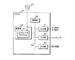
- FIG. 2 is a block diagram showing a main configuration of the microcomputer 27.
- the microcomputer 27 has input units 41 and 42, an output unit 43, a storage unit 44, and a control unit 45. These are connected to the internal bus 46.
- An ON instruction and an OFF instruction are input to the input unit 41.
- the input unit 41 notifies the control unit 45 of the input instruction.
- a high-level voltage and a low-level voltage are input to the input unit 42 from the output terminal of the comparator 25.
- the input unit 42 notifies the input voltage to the control unit 45.
- the output unit 43 outputs a high-level voltage or a low-level voltage to the booster circuit 24.
- the output unit 43 switches the voltage output to the booster circuit 24 to a high-level voltage or a low-level voltage according to an instruction from the control unit 45.
- the storage unit 44 is a nonvolatile memory.
- the storage unit 44 stores a computer program P1.
- the control unit 45 has one or more CPUs (Central Processing Unit). One or a plurality of CPUs included in the control unit 45 execute the computer program P1 to execute a switching process for switching the voltage output to the booster circuit 24 to a high-level voltage or a low-level voltage.
- the computer program P1 is used to cause one or more CPUs of the control unit 45 to execute the switching process.
- the computer program P1 may be stored in the storage medium A1 so as to be readable by one or more CPUs included in the control unit 45.
- the computer program P1 read from the storage medium A1 by a reading device (not shown) is stored in the storage unit 44.
- the storage medium A1 is an optical disk, a flexible disk, a magnetic disk, a magnetic optical disk, a semiconductor memory, or the like.
- the optical disk is a CD (Compact Disc) -ROM (Read Only Memory), a DVD (Digital Versatile Disc) -ROM, or a BD (Blu-ray (registered trademark) Disc).
- the magnetic disk is, for example, a hard disk.
- the computer program P1 may be downloaded from an external device (not shown) connected to a communication network (not shown), and the downloaded computer program P1 may be stored in the storage unit 44.
- FIG. 3 is a flowchart showing the procedure of the switching process.
- the control unit 45 periodically executes the switching process. As described above, when the battery 11 is connected between the positive terminal T1 and the negative terminal T2, power is supplied to the booster circuit 24, the comparator 25, the regulator 26, and the microcomputer 27 regardless of the polarity of the terminal voltage.
- step S1 the control unit 45 determines whether or not the connection of the battery 11 is a normal connection (step S1).
- step S1 when the voltage input from the comparator 25 to the input unit 42 is a high-level voltage, the control unit 45 determines that the connection of the battery 11 is a normal connection.
- the control unit 45 determines that the connection of the battery 11 is not a normal connection, that is, a reverse connection.
- control unit 45 determines that the connection of the battery 11 is not a normal connection (S1: NO)
- the control unit 45 instructs the output unit 43 to switch the voltage output to the booster circuit 24 to a high level voltage (step S2). ).
- the output unit 43 switches the voltage output to the booster circuit 24 to the high level voltage, and the booster circuit 24 applies the boosted voltage to the gate of the semiconductor switch 21.
- the semiconductor switch 21 is turned on.
- the control unit 45 ends the switching process.
- control unit 45 determines whether an ON instruction has been input to the input unit 41 (step S3).
- control unit 45 instructs the output unit 43 to switch the voltage output to the booster circuit 24 to the high-level voltage as in step S2 (S3). Step S4). As a result, the semiconductor switch 21 is turned on.
- control unit 45 determines whether the ON instruction has not been input (S3: NO). If the control unit 45 determines whether the OFF instruction has been input to the input unit 41 (step S5). When determining that the OFF instruction has been input (S5: YES), the control unit 45 instructs the output unit 43 to switch the voltage output to the booster circuit 24 to the low level voltage (step S6). As a result, the output unit 43 switches the voltage output to the booster circuit 24 to the low level voltage, and the booster circuit 24 stops boosting the converted voltage. As a result, the semiconductor switch 21 is turned off.
- the control unit 45 ends the switching process after performing one of steps S4 and S5, or when determining that the OFF instruction has not been input (S5: NO).
- the conversion circuit 23 converts the terminal voltage to a positive voltage regardless of the polarity of the terminal voltage. . Therefore, regardless of the polarity of the terminal voltage, a positive voltage is applied to the booster circuit 24, the comparator 25, the regulator 26, and the microcomputer 27, and power is supplied to these.
- the control unit 45 executes a switching process.
- the switching process when the control unit 45 determines that the connection of the battery 11 is the reverse connection, the booster circuit 24 applies the boosted voltage to the gate of the semiconductor switch 21 and switches the semiconductor switch 21 on.
- the current flows in the order of the negative terminal T2, the load 14, the semiconductor switch 21, the fuse 13, and the positive terminal T1, and no current flows through the parasitic diode 22.
- the output unit 43 changes the voltage output to the booster circuit 24 to high according to the instruction input to the input unit 41. Switch to level voltage or low level voltage.
- the booster circuit 24 applies a boosted voltage to the gate of the semiconductor switch 21 to switch the semiconductor switch 21 ON.
- the semiconductor switch 21 is on, a current flows in the order of the positive terminal T1, the fuse 13, the semiconductor switch 21, the load 14, and the negative terminal T2, and power is supplied to the load 14.
- the booster circuit 24 stops boosting and switches off the semiconductor switch 21. Since the cathode of the parasitic diode 22 is connected to the positive terminal T1, when the semiconductor switch 21 is off, no current flows to the load 14 via the semiconductor switch 21 or the parasitic diode 22, and power is supplied to the load 14. Stops.
- the electric device to which the conversion voltage converted by the conversion circuit 23 is applied is not limited to the booster circuit 24, the comparator 25, the regulator 26, and the microcomputer 27, and is a device that needs to supply power regardless of the polarity of the terminal voltage. Should be fine.
Landscapes
- Engineering & Computer Science (AREA)
- Mechanical Engineering (AREA)
- Power Engineering (AREA)
- Direct Current Feeding And Distribution (AREA)
- Charge And Discharge Circuits For Batteries Or The Like (AREA)
- Dc-Dc Converters (AREA)
Abstract
車両に搭載された給電制御装置(12)では、変換回路(23)は、正極端子(T1)及び負極端子(T2)間に印加される直流電圧の極性に無関係に、所定極性の電圧に変換する。変換回路(23)が変換した電圧に係る電圧は、昇圧回路(24)、コンパレータ(25)、レギュレータ(26)及びマイコン(27)に印加される。
Description
本開示は車載装置に関する。
本出願は、2018年6月28日出願の日本出願第2018-123453号に基づく優先権を主張し、前記日本出願に記載された全ての記載内容を援用するものである。
本出願は、2018年6月28日出願の日本出願第2018-123453号に基づく優先権を主張し、前記日本出願に記載された全ての記載内容を援用するものである。
特許文献1には、直流電源から電力が供給される電気機器を備える車載装置が開示されている。この車載装置では、電源回路にダイオードのカソードが接続されている。
直流電源の正極がダイオードのアノードに接続されている場合、電源回路は、直流電源の出力電圧を降圧し、降圧した電圧を電気機器に印加する。これにより、電気機器に電力が供給され、電気機器が作動する。誤って、直流電源の負極がダイオードのアノードに接続された場合、ダイオードの作用により、電気機器に電力が供給されることはない。
本開示の一態様に係る車載装置は、2つの端子間に直流電圧が印加され、前記2つの端子を介して電気機器に電力が供給される車載装置であって、前記直流電圧の極性に無関係に、前記直流電圧を所定極性の電圧に変換する変換回路を備え、前記変換回路が変換した電圧に係る電圧が前記電気機器に印加される。
[本開示が解決しようとする課題]
特許文献1に記載の車載装置では、誤った直流電源の接続を行った場合、電気機器が作動することはない。しかしながら、直流電源の接続が誤っている場合、即ち、直流電源が接続される2つの端子間に印加される直流電圧の極性が誤っている場合であっても作動しなければならない電気機器が車両に搭載されている可能性がある。
特許文献1に記載の車載装置では、誤った直流電源の接続を行った場合、電気機器が作動することはない。しかしながら、直流電源の接続が誤っている場合、即ち、直流電源が接続される2つの端子間に印加される直流電圧の極性が誤っている場合であっても作動しなければならない電気機器が車両に搭載されている可能性がある。
そこで、2つの端子間に印加される直流電圧の極性に無関係に電気機器に電力を供給することができる車載装置を提供することを目的とする。
[本開示の効果]
本開示によれば、2つの端子間に印加される直流電圧の極性に無関係に電気機器に電力を供給することができる。
本開示によれば、2つの端子間に印加される直流電圧の極性に無関係に電気機器に電力を供給することができる。
[本開示の実施形態の説明]
最初に本開示の実施態様を列挙して説明する。以下に記載する実施形態の少なくとも一部を任意に組み合わせてもよい。
最初に本開示の実施態様を列挙して説明する。以下に記載する実施形態の少なくとも一部を任意に組み合わせてもよい。
(1)本開示の一態様に係る車載装置は、2つの端子間に直流電圧が印加され、前記2つの端子を介して電気機器に電力が供給される車載装置であって、前記直流電圧の極性に無関係に、前記直流電圧を所定極性の電圧に変換する変換回路を備え、前記変換回路が変換した電圧に係る電圧が前記電気機器に印加される。
上記の一態様にあっては、変換回路は、直流電圧の極性に無関係に直流電圧を所定極性の電圧に変換する。このため、2つの端子間に印加される直流電圧の極性に無関係に、所定極性の電圧が電気機器に印加され、電気機器に電力が供給される。
(2)本開示の一態様に係る車載装置は、制御端の電圧が高い程、第1端及び第2端間の抵抗値が小さい半導体スイッチを備え、前記電気機器は、前記変換回路が変換した電圧を昇圧し、昇圧した電圧を前記半導体スイッチの制御端に印加する昇圧回路であり、前記直流電圧は、前記半導体スイッチの前記第1端及び第2端を介して出力される。
上記の一態様にあっては、2つの端子間に印加される直流電圧の極性に無関係に昇圧回路に電力が供給される。昇圧回路は、変換回路が変換した電圧を昇圧し、昇圧した電圧を半導体スイッチの制御端に印加する。これにより、半導体スイッチはオフからオンに切替わる。
(3)本開示の一態様に係る車載装置は、前記変換回路が変換した電圧を降圧し、降圧した電圧を前記電気機器に印加する降圧回路を備える。
上記の一態様にあっては、降圧回路は、変換回路が変換した電圧を降圧し、降圧した電圧を電気機器に印加する。これにより、電気機器に電力が供給される。
(4)本開示の一態様に係る車載装置は、前記変換回路は、アノードが前記2つの端子中の一方の端子に接続される第1ダイオードと、カソードが前記第1ダイオードのカソードに接続され、アノードが前記2つの端子中の他方の端子に接続される第2ダイオードと、カソードが前記一方の端子に接続される第3ダイオードと、アノードが前記第3ダイオードのアノードに接続され、カソードが前記他方の端子に接続される第4ダイオードとを有し、前記変換回路が変換した電圧は、前記第2ダイオードのカソード及び前記第4ダイオードのアノードから出力される。
上記の一態様にあっては、変換回路が電圧を印加する印加対象が第2ダイオードのカソードと、第4ダイオードのアノードとに接続されている。他方の端子の電位を基準とした一方の端子の電圧の極性が正である場合、第1ダイオード、印加対象及び第4ダイオードの順に電流が流れる。他方の端子の電位を基準とした一方の端子の電圧の極性が負である場合、第2ダイオード、印加対象及び第3ダイオードの順に流れる。変換回路が変換した電圧が、第2ダイオードのカソード及び第4ダイオードのアノードから印加対象に出力される。
[本開示の実施形態の詳細]
本開示の実施形態に係る車載装置の具体例を、以下に図面を参照しつつ説明する。なお、本発明はこれらの例示に限定されるものではなく、請求の範囲によって示され、請求の範囲と均等の意味および範囲内でのすべての変更が含まれることが意図される。
本開示の実施形態に係る車載装置の具体例を、以下に図面を参照しつつ説明する。なお、本発明はこれらの例示に限定されるものではなく、請求の範囲によって示され、請求の範囲と均等の意味および範囲内でのすべての変更が含まれることが意図される。
図1は、本実施形態における電源システム1の要部構成を示すブロック図である。電源システム1は、好適に車両に搭載されており、バッテリ11、給電制御装置12、ヒューズ13、負荷14、正極端子T1及び負極端子T2を備える。バッテリ11は、正極端子T1及び負極端子T2間に着脱可能に接続される。バッテリ11が正極端子T1及び負極端子T2間に接続された場合、正極端子T1及び負極端子T2間に直流電圧が印加される。以下では、正極端子T1及び負極端子T2間に印加される直流電圧を端子電圧と記載する。端子電圧は、負極端子T2の電位を基準とした正極端子T1の電圧である。
バッテリ11の正極及び負極夫々が正極端子T1及び負極端子T2に接続された場合、バッテリ11の接続は正常接続であり、端子電圧の極性は正である。バッテリ11の正極及び負極夫々が負極端子T2及び正極端子T1に誤って接続された場合、バッテリ11の接続は逆接続であり、端子電圧の極性は負である。
給電制御装置12は、車載装置であり、半導体スイッチ21、寄生ダイオード22、変換回路23、昇圧回路24、コンパレータ25、レギュレータ26、マイクロコンピュータ(以下、マイコンという)27及び抵抗R1,R2を有する。半導体スイッチ21はNチャネル型のFETである。寄生ダイオード22は、半導体スイッチ21が製造された場合に形成されるダイオードである。コンパレータ25は、電流入力端、電流出力端、プラス端、マイナス端及び電圧出力端を有する。変換回路23は、第1ダイオード31、第2ダイオード32、第3ダイオード33及び第4ダイオード34を有する。
正極端子T1は、ヒューズ13を介して、給電制御装置12の半導体スイッチ21のドレインに接続されている。半導体スイッチ21のソースは負荷14の一端に接続されている。負荷14の他端は負極端子T2に接続されている。
給電制御装置12内では、半導体スイッチ21のドレイン及びソース夫々は、寄生ダイオード22のカソード及びアノードに接続されている。半導体スイッチ21のゲート及びソース間に抵抗R1が接続されている。半導体スイッチ21のゲートは、更に、抵抗R2の一端に接続されている。正極端子T1は、更に、ヒューズ13を介して、変換回路23の第1ダイオード31のアノードに接続されている。変換回路23内では、第1ダイオード31のカソードは、第2ダイオード32のカソードに接続されている。第2ダイオード32のアノードは負極端子T2に接続されている。第2ダイオード32のカソードは、更に、昇圧回路24、コンパレータ25の電流入力端及びレギュレータ26に接続されている。
正極端子T1は、更に、ヒューズ13を介して、変換回路23の第3ダイオード33のカソードに接続されている。変換回路23内では、第3ダイオード33のアノードは、第4ダイオード34のアノードに接続されている。第4ダイオード34のカソードは負極端子T2に接続されている。第4ダイオード34のアノードは、更に、昇圧回路24、コンパレータ25の電流出力端、レギュレータ26及びマイコン27に接続されている。
昇圧回路24は、更に、マイコン27及び抵抗R2の他端に接続されている。コンパレータ25のプラス端は、ヒューズ13を介して、正極端子T1に接続されている。コンパレータ25のマイナス端及び電圧出力端夫々は、負極端子T2及びマイコン27に接続されている。
バッテリ11が正極端子T1及び負極端子T2に接続された場合、変換回路23は、端子電圧を変換し、変換した電圧を昇圧回路24、コンパレータ25及びレギュレータ26に印加する。これにより、昇圧回路24、コンパレータ25及びレギュレータ26に電力が供給される。
以下では、変換回路23が変換した電圧を変換電圧と記載する。変換電圧は、第4ダイオード34のアノードの電位を基準とした第2ダイオード32のカソードの電圧である。変換回路23が変換電圧を印加する3つの印加対象は、昇圧回路24、コンパレータ25及びレギュレータ26である。変換電圧は、変換回路23が変換した電圧であるので、変換回路23が変換した電圧に係る電圧でもある。
バッテリ11の接続が正常接続である場合、即ち、端子電圧の極性が正である場合、電流は、正極端子T1、ヒューズ13、第1ダイオード31、印加対象、第4ダイオード34及び負極端子T2の順に流れる。このとき、変換電圧の極性は正である。
ヒューズ13を流れる電流が所定電流以上となった場合、ヒューズ13は溶断される。
ヒューズ13を流れる電流が所定電流以上となった場合、ヒューズ13は溶断される。
バッテリ11の接続が逆接続である場合、即ち、端子電圧の極性が負である場合、電流は、負極端子T2、第2ダイオード32、印加対象、第3ダイオード33及び正極端子T1の順に流れる。このときも、変換電圧の極性は正である。
以上のように、変換回路23では、端子電圧の極性に無関係に、端子電圧を正の電圧(変換電圧)に変換し、変換電圧は第2ダイオード32のカソード及び第4ダイオード34のアノードから印加対象に出力される。変換電圧は昇圧回路24、コンパレータ25及びレギュレータ26に印加される。端子電圧の極性に無関係に正の電圧が昇圧回路24、コンパレータ25及びレギュレータ26に印加され、正極端子T1及び負極端子T2を介してこれらに電力が供給される。昇圧回路24、コンパレータ25及びレギュレータ26夫々は電気機器として機能する。
変換回路23から昇圧回路24、コンパレータ25及びレギュレータ26に電力が供給されている場合、これらは作動する。変換回路23から昇圧回路24、コンパレータ25及びレギュレータ26への給電が停止した場合、これらは動作を停止する。
半導体スイッチ21について、ソースの電位を基準としたゲートの電圧が高い程、ドレイン及びソース間の抵抗値は小さい。半導体スイッチ21について、ソースの電位を基準としたゲートの電圧が閾値以上である場合、ドレイン及びソース間の抵抗値は小さく、ドレイン及びソースを介して電流を流れることが可能である。このとき、半導体スイッチ21はオンである。
半導体スイッチ21について、ソースの電位を基準としたゲートの電圧が閾値未満である場合、ドレイン及びソース間の抵抗値が大きく、ドレイン及びソースを介して電流を流れることはない。このとき、半導体スイッチ21はオフである。閾値は、一定であり、ゼロVを超えている。半導体スイッチ21のドレイン、ソース及びゲート夫々は、第1端、第2端及び制御端に相当する。
マイコン27は、昇圧回路24にハイレベル電圧又はローレベル電圧を出力している。昇圧回路24は、マイコン27から入力されている電圧がローレベル電圧からハイレベル電圧に切替わった場合、変換電圧を昇圧し、昇圧した電圧を、抵抗R2を介して、半導体スイッチ21のゲートに印加する。以下では、昇圧回路24が昇圧した電圧を昇圧電圧と記載する。昇圧電圧は、第4ダイオード34のアノードの電位を基準とした電圧である。昇圧電圧の極性は正である。
昇圧回路24が昇圧電圧を半導体スイッチ21のゲートに印加した場合、半導体スイッチ21では、バッテリ11の接続、即ち、端子電圧の極性に無関係に、ソースの電位を基準としたゲートの電圧が閾値以上となる。結果、半導体スイッチ21はオンに切替わる。半導体スイッチ21がオンである場合、半導体スイッチ21のドレイン及びソース間の抵抗値は小さい。このため、半導体スイッチ21がオンである場合、電流は、半導体スイッチ21のドレイン及びソースを介して流れ、端子電圧は、半導体スイッチ21のドレイン及びソースを介して出力される。半導体スイッチ21がオンである場合、寄生ダイオード22を介して流れる電流は略ゼロAである。
昇圧回路24は、マイコン27から入力されている電圧がハイレベル電圧からローレベル電圧に切替わった場合、変換電圧の昇圧を停止する。このとき、抵抗R1に電流が流れず、半導体スイッチ21において、ソースの電位を基準としたゲートの電圧は、ゼロVであり、正の閾値未満である。結果、半導体スイッチ21はオフに切替わる。
昇圧回路24が動作を停止している場合、昇圧回路24は昇圧を停止しているため、抵抗R1に電流が流れず、半導体スイッチ21はオフである。
コンパレータ25は、端子電圧がゼロV以上である場合、出力端からハイレベル電圧をマイコン27に出力する。コンパレータ25は、端子電圧がゼロV未満である場合、出力端からローレベル電圧をマイコン27に出力する。
レギュレータ26は、変換回路23が変換した変換電圧を降圧し、降圧した電圧をマイコン27に印加する。以下では、レギュレータ26が降圧した電圧を降圧電圧と記載する。降圧電圧は、第4ダイオード34のアノードの電位を基準とした電圧であり、降圧電圧の極性は正である。降圧電圧は変換回路23が変換した電圧に係る電圧である。レギュレータ26は降圧回路としても機能する。
レギュレータ26が降圧電圧をマイコン27に印加した場合、マイコン27に電力が供給される。マイコン27に電力が供給されている場合、電流は、正極端子T1、ヒューズ13、変換回路23、レギュレータ26、マイコン27、変換回路23及び負極端子T2の順に流れる。
以上のように、降圧電圧がマイコン27に印加され、正極端子T1及び負極端子T2を介してマイコン27に電力が供給される。マイコン27も電気機器として機能する。レギュレータ26からマイコン27に電力が供給されている場合、マイコン27は作動する。レギュレータ26からマイコン27への給電が停止した場合、マイコン27は動作を停止する。
バッテリ11が正極端子T1及び負極端子T2間に接続されている場合、端子電圧の極性に無関係に、レギュレータ26に電力が供給され、レギュレータ26は降圧電圧をマイコン27に印加する。このため、バッテリ11が正極端子T1及び負極端子T2間に接続されている場合、端子電圧の極性に無関係に、マイコン27に電力が供給される。
マイコン27には、半導体スイッチ21のオンを指示するオン指示と、半導体スイッチ21のオフを指示するオフ指示とが入力される。マイコン27は、コンパレータ25から入力された電圧と、入力された指示とに基づいて、昇圧回路24に出力している電圧をハイレベル電圧又はローレベル電圧に切替える。
図2はマイコン27の要部構成を示すブロック図である。マイコン27は、入力部41,42、出力部43、記憶部44及び制御部45を有する。これらは内部バス46に接続されている。
オン指示及びオフ指示が入力部41に入力される。入力部41は、オン指示又はオフ指示が入力された場合、入力された指示を制御部45に通知する。
コンパレータ25の出力端から入力部42にハイレベル電圧及びローレベル電圧が入力される。入力部42は、ハイレベル電圧又はローレベル電圧が入力された場合、入力された電圧を制御部45に通知する。
コンパレータ25の出力端から入力部42にハイレベル電圧及びローレベル電圧が入力される。入力部42は、ハイレベル電圧又はローレベル電圧が入力された場合、入力された電圧を制御部45に通知する。
出力部43は昇圧回路24にハイレベル電圧又はローレベル電圧を出力している。出力部43は、制御部45の指示に従って、昇圧回路24に出力している電圧をハイレベル電圧又はローレベル電圧に切替える。
記憶部44は不揮発性メモリである。記憶部44には、コンピュータプログラムP1が記憶されている。制御部45は、一又は複数のCPU(Central Processing Unit)を有する。制御部45が有する一又は複数のCPUは、コンピュータプログラムP1を実行することによって、昇圧回路24に出力している電圧をハイレベル電圧又はローレベル電圧に切替える切替え処理を実行する。コンピュータプログラムP1は、制御部45が有する一又は複数のCPUに切替え処理を実行させるために用いられる。
なお、コンピュータプログラムP1は、制御部45が有する一又は複数のCPUが読み取り可能に、記憶媒体A1に記憶されていてもよい。この場合、図示しない読み出し装置によって記憶媒体A1から読み出されたコンピュータプログラムP1が記憶部44に記憶される。記憶媒体A1は、光ディスク、フレキシブルディスク、磁気ディスク、磁気光ディスク又は半導体メモリ等である。光ディスクは、CD(Compact Disc)-ROM(Read Only Memory)、DVD(Digital Versatile Disc)-ROM、又は、BD(Blu-ray(登録商標) Disc)等である。磁気ディスクは、例えばハードディスクである。また、図示しない通信網に接続されている図示しない外部装置からコンピュータプログラムP1をダウンロードし、ダウンロードしたコンピュータプログラムP1を記憶部44に記憶してもよい。
図3は、切替え処理の手順を示すフローチャートである。マイコン27に電力が供給されている場合において、制御部45は切替え処理を周期的に実行する。前述したように、バッテリ11が正極端子T1及び負極端子T2間に接続されている場合、端子電圧の極性に無関係に、昇圧回路24、コンパレータ25、レギュレータ26及びマイコン27に電力が供給される。
切替え処理では、まず、制御部45は、バッテリ11の接続が正常接続であるか否かを判定する(ステップS1)。ステップS1では、コンパレータ25から入力部42に入力されている電圧がハイレベル電圧である場合、制御部45は、バッテリ11の接続が正常接続であると判定する。コンパレータ25から入力部42に入力されている電圧がローレベル電圧である場合、制御部45は、バッテリ11の接続が正常接続ではない、即ち、逆接続であると判定する。
制御部45は、バッテリ11の接続が正常接続ではないと判定した場合(S1:NO)、昇圧回路24に出力している電圧のハイレベル電圧への切替えを出力部43に指示する(ステップS2)。これにより、出力部43は、昇圧回路24に出力している電圧をハイレベル電圧に切替え、昇圧回路24は昇圧電圧を半導体スイッチ21のゲートに印加する。結果、半導体スイッチ21はオンに切替わる。
制御部45は、ステップS2を実行した後、切替え処理を終了する。
制御部45は、ステップS2を実行した後、切替え処理を終了する。
制御部45は、バッテリ11の接続が正常接続であると判定した場合(S1:YES)、入力部41にオン指示が入力されたか否かを判定する(ステップS3)。制御部45は、オン指示が入力されたと判定した場合(S3:YES)、ステップS2と同様に、昇圧回路24に出力している電圧のハイレベル電圧への切替えを出力部43に指示する(ステップS4)。これにより、半導体スイッチ21がオンに切替わる。
制御部45は、オン指示が入力されていないと判定した場合(S3:NO)、入力部41にオフ指示が入力されたか否かを判定する(ステップS5)。制御部45は、オフ指示が入力されたと判定した場合(S5:YES)、昇圧回路24に出力している電圧のローレベル電圧への切替えを出力部43に指示する(ステップS6)。これにより、出力部43は、昇圧回路24に出力している電圧をローレベル電圧に切替え、昇圧回路24は変換電圧の昇圧を停止する。結果、半導体スイッチ21はオフに切替わる。
制御部45は、ステップS4,S5の一方を実行した後、又は、オフ指示が入力されていないと判定した場合(S5:NO)、切替え処理を終了する。
以上のように構成された給電制御装置12では、バッテリ11が正極端子T1及び負極端子T2に接続された場合、変換回路23は、端子電圧の極性に無関係に端子電圧を正の電圧に変換する。このため、端子電圧の極性に無関係に、昇圧回路24、コンパレータ25、レギュレータ26及びマイコン27に正の電圧が印加され、これらに電力が供給される。
マイコン27に電力が供給された場合、制御部45は切替え処理を実行する。切替え処理において、バッテリ11の接続が逆接続であると制御部45が判定した場合、昇圧回路24は、昇圧電圧を半導体スイッチ21のゲートに印加し、半導体スイッチ21をオンに切替える。これにより、電流は、負極端子T2、負荷14、半導体スイッチ21、ヒューズ13及び正極端子T1の順に流れ、寄生ダイオード22を電流が流れることはない。
電流が寄生ダイオード22を流れた場合、寄生ダイオード22で大きな電力が消費され、半導体スイッチ21の温度が急速に上昇し、半導体スイッチ21が故障する可能性がある。前述したように、バッテリ11の接続が逆接続である場合、半導体スイッチ21がオンに切替わるので、寄生ダイオード22を電流が流れる時間は短い。結果、半導体スイッチ21の温度が異常な温度となることはなく、半導体スイッチ21が故障する可能性は低い。
切替え処理において、バッテリ11の接続が正常接続であると制御部45が判定した場合、入力部41に入力された指示に応じて、出力部43は、昇圧回路24に出力している電圧をハイレベル電圧又はローレベル電圧に切替える。昇圧回路24は、マイコン27の入力部41にオン指示が入力された場合、昇圧電圧を半導体スイッチ21のゲートに印加し、半導体スイッチ21をオンに切替える。半導体スイッチ21がオンである場合、電流が、正極端子T1、ヒューズ13、半導体スイッチ21、負荷14及び負極端子T2の順に流れ、負荷14に電力が供給される。
昇圧回路24は、マイコン27の入力部41にオフ指示が入力された場合、昇圧を停止し、半導体スイッチ21をオフに切替える。寄生ダイオード22のカソードは正極端子T1に接続されているので、半導体スイッチ21がオフである場合、半導体スイッチ21又は寄生ダイオード22を介して負荷14に電流が流れることはなく、負荷14への給電が停止する。
なお、変換回路23が変換した変換電圧が印加される電気機器は、昇圧回路24、コンパレータ25、レギュレータ26及びマイコン27に限定されず、端子電圧の極性に無関係に電力を供給する必要がある機器であればよい。
開示された本実施形態はすべての点で例示であって、制限的なものではないと考えられるべきである。本発明の範囲は、上述した意味ではなく、請求の範囲によって示され、請求の範囲と均等の意味及び範囲内でのすべての変更が含まれることが意図される。
1 電源システム
11 バッテリ
12 給電制御装置(車載装置)
13 ヒューズ
14 負荷
21 半導体スイッチ
22 寄生ダイオード
23 変換回路
24 昇圧回路(電気機器)
25 コンパレータ(電気機器)
26 レギュレータ(電気機器、降圧回路)
27 マイコン(電気機器)
31 第1ダイオード
32 第2ダイオード
33 第3ダイオード
34 第4ダイオード
41,42 入力部
43 出力部
44 記憶部
45 制御部
46 内部バス
A1 記憶媒体
P1 コンピュータプログラム
R1,R2 抵抗
T1 正極端子
T2 負極端子
11 バッテリ
12 給電制御装置(車載装置)
13 ヒューズ
14 負荷
21 半導体スイッチ
22 寄生ダイオード
23 変換回路
24 昇圧回路(電気機器)
25 コンパレータ(電気機器)
26 レギュレータ(電気機器、降圧回路)
27 マイコン(電気機器)
31 第1ダイオード
32 第2ダイオード
33 第3ダイオード
34 第4ダイオード
41,42 入力部
43 出力部
44 記憶部
45 制御部
46 内部バス
A1 記憶媒体
P1 コンピュータプログラム
R1,R2 抵抗
T1 正極端子
T2 負極端子
Claims (4)
- 2つの端子間に直流電圧が印加され、前記2つの端子を介して電気機器に電力が供給される車載装置であって、
前記直流電圧の極性に無関係に、前記直流電圧を所定極性の電圧に変換する変換回路を備え、
前記変換回路が変換した電圧に係る電圧が前記電気機器に印加される
車載装置。 - 制御端の電圧が高い程、第1端及び第2端間の抵抗値が小さい半導体スイッチを備え、
前記電気機器は、前記変換回路が変換した電圧を昇圧し、昇圧した電圧を前記半導体スイッチの制御端に印加する昇圧回路であり、
前記直流電圧は、前記半導体スイッチの前記第1端及び第2端を介して出力される
請求項1に記載の車載装置。 - 前記変換回路が変換した電圧を降圧し、降圧した電圧を前記電気機器に印加する降圧回路を備える
請求項1に記載の車載装置。 - 前記変換回路は、
アノードが前記2つの端子中の一方の端子に接続される第1ダイオードと、
カソードが前記第1ダイオードのカソードに接続され、アノードが前記2つの端子中の他方の端子に接続される第2ダイオードと、
カソードが前記一方の端子に接続される第3ダイオードと、
アノードが前記第3ダイオードのアノードに接続され、カソードが前記他方の端子に接続される第4ダイオードと
を有し、
前記変換回路が変換した電圧は、前記第2ダイオードのカソード及び前記第4ダイオードのアノードから出力される
請求項1から請求項3のいずれか1つに記載の車載装置。
Applications Claiming Priority (2)
| Application Number | Priority Date | Filing Date | Title |
|---|---|---|---|
| JP2018123453A JP2020005420A (ja) | 2018-06-28 | 2018-06-28 | 車載装置 |
| JP2018-123453 | 2018-06-28 |
Publications (1)
| Publication Number | Publication Date |
|---|---|
| WO2020003985A1 true WO2020003985A1 (ja) | 2020-01-02 |
Family
ID=68986397
Family Applications (1)
| Application Number | Title | Priority Date | Filing Date |
|---|---|---|---|
| PCT/JP2019/022859 Ceased WO2020003985A1 (ja) | 2018-06-28 | 2019-06-10 | 車載装置 |
Country Status (2)
| Country | Link |
|---|---|
| JP (1) | JP2020005420A (ja) |
| WO (1) | WO2020003985A1 (ja) |
Citations (2)
| Publication number | Priority date | Publication date | Assignee | Title |
|---|---|---|---|---|
| JPH09285003A (ja) * | 1996-04-09 | 1997-10-31 | Harness Sogo Gijutsu Kenkyusho:Kk | 車両におけるバッテリー接続回路 |
| JP2011259627A (ja) * | 2010-06-09 | 2011-12-22 | Panasonic Corp | 電源逆接続保護回路 |
-
2018
- 2018-06-28 JP JP2018123453A patent/JP2020005420A/ja active Pending
-
2019
- 2019-06-10 WO PCT/JP2019/022859 patent/WO2020003985A1/ja not_active Ceased
Patent Citations (2)
| Publication number | Priority date | Publication date | Assignee | Title |
|---|---|---|---|---|
| JPH09285003A (ja) * | 1996-04-09 | 1997-10-31 | Harness Sogo Gijutsu Kenkyusho:Kk | 車両におけるバッテリー接続回路 |
| JP2011259627A (ja) * | 2010-06-09 | 2011-12-22 | Panasonic Corp | 電源逆接続保護回路 |
Also Published As
| Publication number | Publication date |
|---|---|
| JP2020005420A (ja) | 2020-01-09 |
Similar Documents
| Publication | Publication Date | Title |
|---|---|---|
| US10654428B2 (en) | Power supply control device | |
| CN110021971B (zh) | 供电控制装置及供电控制方法 | |
| WO2018180753A1 (ja) | 電源装置 | |
| JP7363955B2 (ja) | 給電制御装置、給電制御方法及びコンピュータプログラム | |
| US20240079960A1 (en) | Voltage conversion device | |
| JP6376422B2 (ja) | 充放電装置 | |
| EP3038223A1 (en) | Load driving circuit | |
| WO2017043311A1 (ja) | 車載用電源装置 | |
| US20190165561A1 (en) | Power supply control apparatus, power supply control method, and computer program | |
| WO2020183901A1 (ja) | 通電制御装置 | |
| WO2020022037A1 (ja) | 回路装置 | |
| CN107408828B (zh) | 控制车辆的电路的电力供应的包含电池和相关组件的设备 | |
| JP2020005420A (ja) | 車載装置 | |
| JP2018074874A (ja) | 電子制御装置 | |
| WO2021033630A1 (ja) | スイッチ装置 | |
| CN111247740B (zh) | 输出装置及电源系统 | |
| CN108702015A (zh) | 放电电路以及蓄电装置 | |
| CN116490404A (zh) | 供电控制装置、供电控制方法及计算机程序 | |
| CN116057836A (zh) | 检测电路及供电控制装置 | |
| CN115315870B (zh) | 供电控制装置、检查方法和计算机程序产品 | |
| US11870427B2 (en) | Power supply control device | |
| JP7619210B2 (ja) | 給電制御装置、給電制御方法及びコンピュータプログラム | |
| JP6387498B2 (ja) | 二次電池の充電制御回路 | |
| JP7366319B2 (ja) | 制御装置、電力変換装置および制御方法 | |
| JP2025068767A (ja) | 故障検出装置 |
Legal Events
| Date | Code | Title | Description |
|---|---|---|---|
| 121 | Ep: the epo has been informed by wipo that ep was designated in this application |
Ref document number: 19826476 Country of ref document: EP Kind code of ref document: A1 |
|
| NENP | Non-entry into the national phase |
Ref country code: DE |
|
| 122 | Ep: pct application non-entry in european phase |
Ref document number: 19826476 Country of ref document: EP Kind code of ref document: A1 |