WO2020003930A1 - 車載用の温度検出回路 - Google Patents
車載用の温度検出回路 Download PDFInfo
- Publication number
- WO2020003930A1 WO2020003930A1 PCT/JP2019/022249 JP2019022249W WO2020003930A1 WO 2020003930 A1 WO2020003930 A1 WO 2020003930A1 JP 2019022249 W JP2019022249 W JP 2019022249W WO 2020003930 A1 WO2020003930 A1 WO 2020003930A1
- Authority
- WO
- WIPO (PCT)
- Prior art keywords
- conductive path
- voltage
- bipolar transistor
- electrically connected
- emitter
- Prior art date
- Legal status (The legal status is an assumption and is not a legal conclusion. Google has not performed a legal analysis and makes no representation as to the accuracy of the status listed.)
- Ceased
Links
Images


Classifications
-
- G—PHYSICS
- G01—MEASURING; TESTING
- G01K—MEASURING TEMPERATURE; MEASURING QUANTITY OF HEAT; THERMALLY-SENSITIVE ELEMENTS NOT OTHERWISE PROVIDED FOR
- G01K7/00—Measuring temperature based on the use of electric or magnetic elements directly sensitive to heat ; Power supply therefor, e.g. using thermoelectric elements
- G01K7/16—Measuring temperature based on the use of electric or magnetic elements directly sensitive to heat ; Power supply therefor, e.g. using thermoelectric elements using resistive elements
- G01K7/18—Measuring temperature based on the use of electric or magnetic elements directly sensitive to heat ; Power supply therefor, e.g. using thermoelectric elements using resistive elements the element being a linear resistance, e.g. platinum resistance thermometer
- G01K7/20—Measuring temperature based on the use of electric or magnetic elements directly sensitive to heat ; Power supply therefor, e.g. using thermoelectric elements using resistive elements the element being a linear resistance, e.g. platinum resistance thermometer in a specially-adapted circuit, e.g. bridge circuit
-
- G—PHYSICS
- G01—MEASURING; TESTING
- G01K—MEASURING TEMPERATURE; MEASURING QUANTITY OF HEAT; THERMALLY-SENSITIVE ELEMENTS NOT OTHERWISE PROVIDED FOR
- G01K1/00—Details of thermometers not specially adapted for particular types of thermometer
- G01K1/02—Means for indicating or recording specially adapted for thermometers
- G01K1/026—Means for indicating or recording specially adapted for thermometers arrangements for monitoring a plurality of temperatures, e.g. by multiplexing
-
- G—PHYSICS
- G01—MEASURING; TESTING
- G01K—MEASURING TEMPERATURE; MEASURING QUANTITY OF HEAT; THERMALLY-SENSITIVE ELEMENTS NOT OTHERWISE PROVIDED FOR
- G01K13/00—Thermometers specially adapted for specific purposes
-
- G—PHYSICS
- G01—MEASURING; TESTING
- G01K—MEASURING TEMPERATURE; MEASURING QUANTITY OF HEAT; THERMALLY-SENSITIVE ELEMENTS NOT OTHERWISE PROVIDED FOR
- G01K7/00—Measuring temperature based on the use of electric or magnetic elements directly sensitive to heat ; Power supply therefor, e.g. using thermoelectric elements
- G01K7/16—Measuring temperature based on the use of electric or magnetic elements directly sensitive to heat ; Power supply therefor, e.g. using thermoelectric elements using resistive elements
- G01K7/22—Measuring temperature based on the use of electric or magnetic elements directly sensitive to heat ; Power supply therefor, e.g. using thermoelectric elements using resistive elements the element being a non-linear resistance, e.g. thermistor
- G01K7/24—Measuring temperature based on the use of electric or magnetic elements directly sensitive to heat ; Power supply therefor, e.g. using thermoelectric elements using resistive elements the element being a non-linear resistance, e.g. thermistor in a specially-adapted circuit, e.g. bridge circuit
-
- G—PHYSICS
- G01—MEASURING; TESTING
- G01K—MEASURING TEMPERATURE; MEASURING QUANTITY OF HEAT; THERMALLY-SENSITIVE ELEMENTS NOT OTHERWISE PROVIDED FOR
- G01K7/00—Measuring temperature based on the use of electric or magnetic elements directly sensitive to heat ; Power supply therefor, e.g. using thermoelectric elements
- G01K7/16—Measuring temperature based on the use of electric or magnetic elements directly sensitive to heat ; Power supply therefor, e.g. using thermoelectric elements using resistive elements
Definitions
- the present invention relates to a temperature detection circuit for a vehicle.
- the present invention has been made based on the above-described circumstances, and has as its object to realize a vehicle-mounted temperature detection circuit that can determine the presence or absence of a temperature abnormality for a plurality of semiconductor elements with a simpler configuration. I do.
- the vehicle-mounted temperature detection circuit of the present invention includes: A temperature detection unit including a plurality of individual detection units each including a resistor and a temperature detection element connected in series between a first conductive path to which a predetermined power supply voltage is applied and a reference conductive path; A plurality of bipolar transistors connected to each of the plurality of individual detection units; A second conductive path electrically connected to an emitter of each of the plurality of bipolar transistors; With Each of the bipolar transistors has a base electrically connected to a third conductive path between the resistor and the temperature detection element of the individual detection unit, A voltage reflecting the highest voltage or the lowest voltage among the voltages applied to each of the third conductive paths in the plurality of individual detection units is applied to the second conductive path.
- a voltage based on the temperature detected by the temperature detection element is applied to the third conductive path between the temperature detection element and the resistor. Then, the voltage applied to each third conductive path is applied to the base of the bipolar transistor connected to each third conductive path. Then, a voltage reflecting the highest voltage or the lowest voltage among the voltages applied to the respective third conductive paths in the plurality of individual detection units is applied to the second conductive path. That is, a voltage based on the highest detected temperature or a voltage based on the lowest detected temperature among the detected temperatures detected by the plurality of temperature detecting elements is applied to the second conductive path.
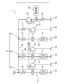
- FIG. 2 is a circuit diagram illustrating a temperature detection circuit for mounting on a vehicle according to the first embodiment.
- FIG. 4 is an explanatory diagram illustrating the operation of the vehicle-mounted temperature detection circuit according to the first embodiment.
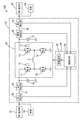
- FIG. 1 is an explanatory diagram illustrating the configuration of a vehicle-mounted power supply system equipped with a vehicle-mounted temperature detection circuit according to a first embodiment.
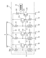
- FIG. 9 is a circuit diagram illustrating a temperature detection circuit for mounting on a vehicle according to a second embodiment.
- FIG. 9 is an explanatory diagram illustrating the operation of the vehicle-mounted temperature detection circuit according to the second embodiment.
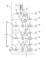
- FIG. 13 is a circuit diagram illustrating a temperature detection circuit for mounting on a vehicle according to a third embodiment.
- each of the plurality of bipolar transistors may be a PNP-type bipolar transistor whose collector is electrically connected to the reference conductive path. Further, a voltage reflecting the lowest voltage among the voltages applied to the respective third conductive paths in the plurality of individual detection units may be applied to the second conductive path.
- the bipolar transistor is a PNP-type bipolar transistor, current can flow from the emitter side to the base side. Further, the respective emitters of the bipolar transistors are connected to the second conductive path so that they have the same potential.
- the base voltage corresponds to a voltage drop between the base and the emitter.
- the voltage to which the predetermined voltage is applied is applied to the second conductive path, and as a result, the base voltage of the other bipolar transistor becomes higher than the voltage lower than the emitter voltage by the predetermined voltage. Therefore, no current flows between the base and the emitter of another bipolar transistor. Accordingly, the voltage of the second conductive path is stabilized at a voltage obtained by adding the predetermined voltage to the lowest voltage among the bases of the respective bipolar transistors. Therefore, according to this configuration, a voltage reflecting the lowest voltage among the voltages applied to the bases of the bipolar transistors can be applied to the second conductive path.
- the bipolar transistor when the bipolar transistor is a PNP type bipolar transistor, the following configuration may be adopted.
- a second resistor having one end electrically connected to the first conductive path and the other end electrically connected to the second conductive path; and a second bipolar transistor including an NPN-type bipolar transistor different from the plurality of bipolar transistors.
- the transistor may include a third resistor having one end electrically connected to the emitter of the second bipolar transistor and the other end electrically connected to the reference conductive path.
- the second bipolar transistor may have a base electrically connected to the second conductive path and a collector electrically connected to the first conductive path.
- a voltage reflecting the voltage of the fourth conductive path between the emitter of the second bipolar transistor and one end of the third resistor may be output.
- the voltage increased between the base and the emitter of the bipolar transistor is canceled between the base and the emitter of the second bipolar transistor.
- the voltage before rising between the base and the emitter of the bipolar transistor that is, the lowest voltage among the voltages applied to the respective bases of the bipolar transistor
- the voltage before rising between the base and the emitter of the bipolar transistor that is, the lowest voltage among the voltages applied to the respective bases of the bipolar transistor
- a voltage reflecting the voltage of the fourth conductive path between the emitter of the second bipolar transistor and one end of the second resistor is output.
- each of the plurality of bipolar transistors may be an NPN-type bipolar transistor whose collector is electrically connected to the first conductive path.
- a plurality of second resistors may be provided in association with each of the plurality of bipolar transistors.
- the second resistor may have one end electrically connected to the emitter of the bipolar transistor associated with the second resistor, and the other end electrically connected to the reference conductive path.
- the second conductive path may be electrically connected to each fourth conductive path connecting between each emitter of each bipolar transistor and one end of each second resistor.
- a voltage reflecting the highest voltage among the voltages applied to the respective third conductive paths in the plurality of individual detection units may be applied to the second conductive path.
- the bipolar transistor When the bipolar transistor is an NPN-type bipolar transistor, current can flow from the base to the emitter. Further, the respective emitters of the bipolar transistors are connected to the second conductive path so that they have the same potential. Therefore, when a current flows from the base to which the highest voltage is applied among the respective bases of the bipolar transistor to the second conductive path (that is, the emitter), a predetermined voltage (a voltage drop between the base and the emitter) decreases from the highest voltage. The corresponding voltage is applied to the second conductive path, so that the base voltage of the other bipolar transistor becomes lower than the voltage obtained by adding the predetermined voltage to the emitter voltage. As a result, no current flows between the base and the emitter of another bipolar transistor.
- a predetermined voltage a voltage drop between the base and the emitter
- the voltage of the second conductive path is stabilized at a voltage lower than the highest voltage among the respective bases of the bipolar transistor by the predetermined voltage. Therefore, according to this configuration, a voltage reflecting the highest voltage among the voltages applied to the respective bases of the bipolar transistor can be applied to the second conductive path.
- the bipolar transistor is an NPN-type bipolar transistor
- a second bipolar transistor comprising a PNP-type bipolar transistor different from the plurality of bipolar transistors, one end of which is electrically connected to the emitter of the second bipolar transistor and the other end of which is electrically connected to the first conductive path; And a third resistor.
- the second bipolar transistor has a base electrically connected to the second conductive path, a collector electrically connected to the reference conductive path, and a second transistor connected between the emitter of the second bipolar transistor and one end of the third resistor.
- a voltage reflecting the voltage of the fifth conductive path may be output.
- the voltage dropped between the base and the emitter of the bipolar transistor is canceled between the base and the emitter of the second bipolar transistor.
- the voltage before dropping between the base and the emitter of the bipolar transistor that is, the highest voltage among the voltages applied to the respective bases of the bipolar transistor
- the voltage before dropping between the base and the emitter of the bipolar transistor is applied to the emitter of the second bipolar transistor.
- a voltage reflecting the voltage of the fifth conductive path between the emitter of the second bipolar transistor and one end of the third resistor is output.
- a temperature detection circuit 1 for mounting on a vehicle shown in FIG. 1 (hereinafter also referred to as a temperature detection circuit 1) individually detects the temperatures of a plurality of semiconductor elements mounted on a vehicle, and based on the detected temperatures, the semiconductor elements. This is to determine the presence or absence of the temperature abnormality.
- the temperature detection circuit 1 mainly includes a temperature detection unit 8, a plurality of bipolar transistors 16, a second conductive path 18, a bipolar transistor 20, a control unit 24, and the like.
- the temperature detector 8 includes a plurality (three in the examples shown in FIGS. 1 and 2) of individual detectors 10.
- Each of the individual detection units 10 is provided between the first conductive path 90 to which a voltage based on the output voltage (Vcc) of the power supply unit is applied and the reference conductive path 92.
- the voltage of the first conductive path 90 that is, the potential difference between the potential of the first conductive path 90 and the potential of the reference conductive path 92 is maintained at a predetermined power supply voltage (Vcc).
- the reference conductive path 92 is a conductive path whose potential is maintained at a predetermined ground potential (for example, 0 V).
- Each of the individual detection units 10 has a configuration in which a first resistor 12 and a temperature detection element 14 are connected in series.
- the temperature detecting element 14 is, for example, an NTC thermistor (Negative ⁇ Temperature ⁇ Coefficient @ Thermistor), and is configured as an element whose resistance decreases as the detection temperature increases. Note that the first resistor 12 corresponds to an example of the resistor of the present invention.
- the bipolar transistor 16 is configured as, for example, a PNP-type bipolar transistor.
- the plurality of bipolar transistors 16 are connected to each of the plurality of individual detection units 10 in association with each other.
- the base of the bipolar transistor 16 is electrically connected to the third conductive path 15 between the first resistor 12 and the temperature detecting element 14 of the individual detecting unit 10 associated with the bipolar transistor 16.
- the bipolar transistor 16 has an emitter electrically connected to the second conductive path 18 and a collector electrically connected to the reference conductive path 92. Note that the bipolar transistor 16 corresponds to an example of the bipolar transistor of the present invention.
- the second conductive path 18 is electrically connected to the respective emitters of the plurality of bipolar transistors 16 and makes the connected emitters the same potential.
- the second conductive path 18 is electrically connected to the first conductive path 90 via the second resistor 17.
- One end of the second resistor 17 is electrically connected to the second conductive path 18, and the other end is electrically connected to the first conductive path 90.
- the bipolar transistor 20 is configured as, for example, an NPN-type bipolar transistor.
- the bipolar transistor 20 has a base connected to the second conductive path 18, a collector connected to the first conductive path 90, and an emitter connected to the control unit 24 and one end of the third resistor 22.
- the other end of the third resistor 22 is connected to the reference conductive path 92.
- the bipolar transistor 20 corresponds to an example of the second bipolar transistor of the present invention.
- the control unit 24 is a unit that determines the presence or absence of a temperature abnormality based on the temperature detected by the temperature detection element 14.
- the control unit 24 includes, for example, a microcomputer and the like, and includes an arithmetic unit such as a CPU, a memory such as a ROM or a RAM, an AD converter, and the like.
- the control unit 24 is electrically connected to the fourth conductive path 23 between the emitter of the bipolar transistor 20 and the third resistor 22.
- the control unit 24 detects a voltage reflecting the voltage applied to the fourth conductive path 23, detects a voltage applied to the emitter of the bipolar transistor 20, and determines whether there is a temperature abnormality based on the detected value. .
- the operation of the temperature detection circuit 1 will be described.
- the temperature detecting element 14 is an NTC thermistor
- the voltage of the third conductive path 15 between the temperature detecting element 14 and the first resistor 12 increases as the temperature detected by the temperature detecting element 14 increases.
- the base of the bipolar transistor 16 is electrically connected to the third conductive path 15, a voltage that decreases as the temperature detected by the temperature detection element 14 increases is applied to the base of the bipolar transistor 16.
- the bipolar transistor 16 is a PNP-type bipolar transistor, a current flows from the emitter side to the base side between the base and the emitter. However, the emitters of the bipolar transistor 16 are electrically connected to each other via the second conductive path 18 and have the same potential. For this reason, in the bipolar transistor 16 having the lowest base voltage, when a current flows from the emitter side to the base side, the voltage of the second conductive path 18 and the emitter of the other bipolar transistor 16 decrease in voltage to the lowest base voltage. It is a voltage to which a corresponding predetermined voltage Vf (for example, 0.6 V) is applied.
- Vf for example, 0.6 V
- the base voltage of the other bipolar transistor 16 becomes higher than a voltage lower than the emitter voltage by a predetermined voltage Vf, so that no current flows between the base and the emitter of the other bipolar transistor 16.
- the voltage of the second conductive path 18 is a voltage obtained by adding the predetermined voltage Vf to the lowest voltage among the voltages applied to each base of the bipolar transistor 16 (the voltage applied to each base of the bipolar transistor 16). (The voltage that reflects the lowest voltage among them).
- the base of the bipolar transistor 20 is electrically connected to the second conductive path 18, and the bipolar transistor 20 is an NPN-type bipolar transistor. Therefore, a voltage lower than the base voltage of the bipolar transistor 20 by a predetermined voltage Vf is applied to the emitter (the fourth conductive path 23) of the bipolar transistor 20.
- Vf a voltage lower than the base voltage of the bipolar transistor 20 by a predetermined voltage Vf is applied to the emitter (the fourth conductive path 23) of the bipolar transistor 20.
- 2.0 V which is 0.6 V lower than the voltage of 2.6 V applied to the second conductive path 18 is applied to the emitter of the bipolar transistor 20 (the fourth conductive path 23). That is, a voltage that cancels the voltage drop between the base and the emitter of the bipolar transistor 16 is applied to the emitter (the fourth conductive path 23) of the bipolar transistor 20.
- a voltage reflecting the voltage of the fourth conductive path 23 is output to the control unit 24.
- the control unit 24 By detecting the voltage of the fourth conductive path 23, the control unit 24 detects the lowest base voltage among the base voltages of the bipolar transistors 16 (that is, the highest detected temperature among the detected temperatures of the plurality of temperature detecting elements 14). ). Therefore, the control unit 24 can determine, for example, whether or not there is a temperature abnormality (whether or not it is overheated) by determining whether or not the detected voltage is lower than a predetermined threshold voltage.
- the on-vehicle power supply system 100 includes a voltage converter 50, a first power supply unit 52, and a second power supply unit 54, and supplies power to on-vehicle loads such as the loads 56 and 58. It is configured as a supplyable system.
- the voltage converter 50 is configured as, for example, a step-up / step-down DCDC converter for use in a vehicle and includes a voltage converter 60.
- the voltage conversion unit 60 includes a primary conductive path 41 to which the high-potential terminal of the first power supply unit 52 and the load 56 are connected, and a second conductive path 41 to which the high-potential terminal of the second power supply unit 54 is connected. It is provided between the secondary side conductive path 42.
- the voltage converter 60 includes switching elements T1, T2, T3, T4 arranged in an H-bridge structure, and an inductor L, and functions as a so-called bidirectional DCDC converter. That is, the function of increasing or decreasing the voltage applied to the primary-side conductive path 41 and outputting the voltage to the secondary-side conductive path 42 and the function of increasing or decreasing the voltage applied to the secondary-side conductive path 42 to increase or decrease the primary-side conductive path It has a function of outputting to the road 41.
- a capacitor 70 is connected to the primary-side conductive path 41, and a capacitor 72 is connected to the secondary-side conductive path 42.
- the voltage converter 50 includes voltage detectors 62 and 64 for detecting the voltage of the primary conductive path 41 and the voltage of the secondary conductive path 42, respectively, and the current of the primary conductive path 41 and the current of the secondary conductive path 42. And current detection units 66 and 68 for respectively detecting The detection values of the voltage detection units 62 and 64 and the detection values of the current detection units 66 and 68 are output to the control unit 24.
- the control unit 24 includes a control circuit 80 (for example, a microcomputer) and a drive circuit 82, and switches the switching elements T1 and T2 based on the detection values of the voltage detection units 62 and 64 or the detection values of the current detection units 66 and 68. , T3, and T4, the voltage conversion unit 60 can be driven to perform a step-up operation or a step-down operation.
- the switching elements T1, T2, T3, and T4 are turned on and off at a high speed when performing the step-up operation or the step-down operation, so that the switching elements T1, T2, T3, and T4 generate heat. For this reason, it is necessary to monitor the temperature around the switching elements T1, T2, T3, T4 so as not to be overheated. Therefore, in the example shown in FIG. 3, the temperature detecting element 14 is provided near the switching elements T1, T2, T3, and T4. Further, in the example shown in FIG. 3, among the four switching elements T1, T2, T3, T4, only some (two in FIG. 3) switching elements are installed. Specifically, one inductor L is provided on each of the primary conductive path 41 and the secondary conductive path 42.
- the temperature detection element 14 When the temperature detection element 14 is provided only for some of the switching elements, it is preferable to provide the temperature detection element 14 for a switching element that easily generates heat. For example, for a switching element that is likely to generate heat as a result of actual operation. It may be installed.
- the voltage based on the temperature detected by the NTC thermistor (temperature detection element 14) in each of the individual detection units 10 is between the temperature detection element 14 and the first resistor 12. Applied to the third conductive path 15. Then, the voltage applied to each third conductive path 15 is applied to the base of a PNP-type bipolar transistor (bipolar transistor 16) connected to each third conductive path 15. The voltage reflecting the lowest voltage (that is, the voltage based on the highest detected temperature) among the voltages applied to the third conductive paths 15 in the plurality of individual detection units 10 is applied to the second conductive path 18. Applied.
- control unit 24 can determine the presence or absence of the overheating state (abnormal temperature) for the plurality of switching elements based on the voltage reflecting the voltage of the second conductive path 18. Therefore, according to the temperature detection circuit 1, it is possible to determine the presence or absence of a temperature abnormality for a plurality of switching elements with a simple configuration.
- the controller 24 outputs a voltage reflecting the voltage of the fourth conductive path 23 between the emitter of the bipolar transistor 20 and one end of the third resistor 22. That is, the control unit 24 can detect, by the bipolar transistor 20, a voltage reflecting a voltage in which an increase due to a voltage drop between the base and the emitter of the bipolar transistor 16 is canceled. For this reason, the control unit 24 does not need to consider the effect of the voltage drop between the base and the emitter of the bipolar transistor 16, and can simplify the process of determining whether or not the overheat condition is present.
- the bipolar transistor is a PNP-type bipolar transistor.
- the bipolar transistor is an NPN-type bipolar transistor.
- the temperature detection circuit 201 mainly includes a temperature detection unit 8, a plurality of bipolar transistors 216, a second conductive path 218, a bipolar transistor 220, a control unit 24, and the like.
- the temperature detector 8 includes a plurality (three in the example shown in FIG. 4.5) of individual detectors 10.
- the individual detection units 10 are provided between the first conductive path 90 and the reference conductive path 92, respectively.
- Each of the individual detection units 10 has a configuration in which a first resistor 12 and a temperature detection element 14 are connected in series.
- the bipolar transistor 216 is configured as, for example, an NPN-type bipolar transistor.
- the plurality of bipolar transistors 216 are connected to each of the plurality of individual detection units 10 in association with each other.
- the base of the bipolar transistor 216 is electrically connected to the third conductive path 15 of the individual detection unit 10 associated with itself.
- Each collector of each bipolar transistor 216 is electrically connected to the first conductive path 90, respectively.
- Each of the plurality of bipolar transistors 216 is provided with a plurality of second resistors 217 in association with each other.
- the second resistor 217 has one end electrically connected to the emitter of the bipolar transistor 216 associated with itself, and the other end electrically connected to the reference conductive path 92.
- a second conductive path 218 is electrically connected to each fourth conductive path 219 connecting between each emitter of each bipolar transistor 216 and one end of each second resistor 217.
- the bipolar transistor 216 corresponds to an example of the bipolar transistor of the present invention.
- the bipolar transistor 220 is configured as a PNP-type bipolar transistor.
- Bipolar transistor 220 has a base electrically connected to second conductive path 218, a collector electrically connected to reference conductive path 92, and an emitter connected to one end of third resistor 222. .
- the other end of the third resistor 222 is electrically connected to the first conductive path 90.
- the control unit 24 is electrically connected to a fifth conductive path 223 between the emitter of the bipolar transistor 220 and the third resistor 222.
- the bipolar transistor 220 corresponds to an example of the second bipolar transistor of the present invention.
- the bipolar transistor 216 is an NPN-type bipolar transistor, a current flows from the base side to the emitter side between the base and the emitter.
- the emitters of the bipolar transistor 216 are connected to each other via the second conductive path 218 and have the same potential. Therefore, when a current flows from the base side to the emitter side in the bipolar transistor 216 having the highest base voltage, the voltage of the second conductive path 218 and the emitter of the other bipolar transistor 216 decrease from the highest base voltage to a voltage drop.
- the voltage is reduced by a corresponding predetermined voltage Vf (for example, 0.6 V).
- the base voltage of the other bipolar transistor 216 becomes lower than the voltage obtained by adding the predetermined voltage Vf to the emitter voltage, so that no current flows between the base and the emitter of the other bipolar transistor 216.
- the voltage of the second conductive path 218 is reduced by a predetermined voltage Vf from the highest voltage among the voltages applied to the respective bases of the bipolar transistors 216 (the voltage of the voltage applied to the respective bases of the bipolar transistors 216). (The voltage that reflects the highest voltage).
- the base of the bipolar transistor 220 is connected to the second conductive path 218, and the bipolar transistor 220 is a PNP-type bipolar transistor. Therefore, a voltage obtained by adding the predetermined voltage Vf from the base voltage of the bipolar transistor 220 is applied to the emitter of the bipolar transistor 220. In the example shown in FIG. 5, 4 V obtained by adding 0.6 V from 3.4 V applied to second conductive path 218 is applied to the emitter of bipolar transistor 220. That is, a voltage that cancels the voltage drop between the base and the emitter of the bipolar transistor 216 is applied to the emitter of the bipolar transistor 220.
- the control unit 24 detects the voltage applied to the emitter of the bipolar transistor 220 to thereby determine the highest base voltage among the base voltages of the bipolar transistors 216 (that is, the highest base voltage among the detected temperatures of the plurality of temperature detecting elements 14). Voltage based on a low detection temperature). Therefore, the control unit 24 can determine whether or not there is a temperature abnormality (whether or not the temperature is low), for example, by determining whether or not the detected voltage is equal to or higher than a predetermined threshold voltage.
- Example 3 In Example 1, the temperature detecting element was an NTC thermistor. On the other hand, in the third embodiment, the temperature detecting element is a PTC thermistor (Positive Temperature Coefficient Thermistor).
- the temperature detection circuit 301 of the third embodiment includes a temperature detection unit 308 instead of the temperature detection unit 8 of the first embodiment, as shown in FIG.
- the temperature detecting section 308 includes a plurality (three in the example shown in FIG. 6) of individual detecting sections 310.
- Each of the individual detection units 310 is provided between the first conductive path 90 and the reference conductive path 92.
- Each of the individual detection units 310 has a configuration in which the first resistor 12 and the temperature detection element 314 are connected in series.
- the temperature detection element 314 is configured as, for example, a PTC thermistor (an element whose resistance increases as the detection temperature increases).
- the arrangement of the first resistor 12 and the temperature detection element 314 is opposite to the arrangement of the first resistor 12 and the temperature detection element 14 in the first embodiment. That is, one end of the temperature detecting element 314 is electrically connected to the first conductive path 90, and the other end of the temperature detecting element 314 is electrically connected to one end of the first resistor 12. The other end of the first resistor 12 is electrically connected to the reference conductive path 92.
- the temperature detection element is changed from the NTC thermistor to the PTC thermistor.
- the temperature detection element 314 and the first resistor 12 are connected.
- the voltage applied to the third conductive path 315 decreases as the temperature detected by the temperature detecting element 314 increases. Therefore, as in the case of the first embodiment, the voltage based on the highest detected temperature is applied to the second conductive path 18, and the voltage that cancels the voltage drop that has risen between the base and the emitter of the bipolar transistor 16 becomes the bipolar transistor. 20 are applied to the emitters.
- a voltage that decreases as the detection temperatures of the plurality of temperature detection elements 14 increase is applied to the bases of the bipolar transistors 16 and 216.
- a voltage that increases as the detection temperatures of the plurality of temperature detection elements 14 increase may be applied to the bases of the bipolar transistors 16 and 216.
- the arrangement of the first resistor 12 and the temperature detection element 14 may be switched while the temperature detection element 14 is an NTC thermistor.
- the temperature detection element 14 may be a PTC thermistor without replacing the arrangement of the first resistor 12 and the temperature detection element 14.
- the control unit 24 detects the voltage applied to the emitters of the bipolar transistors 20 and 220, and determines whether there is a temperature abnormality based on the detected value.
- the control unit 24 may detect the voltage applied to the second conductive paths 18 and 218 and determine whether there is a temperature abnormality based on the detected value. This eliminates the need for the bipolar transistors 20 and 220, thereby reducing the number of components.
- the number of the individual detection units 10 and 310 is three, but may be two or four or more.
Landscapes
- Physics & Mathematics (AREA)
- General Physics & Mathematics (AREA)
- Nonlinear Science (AREA)
- Measuring Temperature Or Quantity Of Heat (AREA)
- Electric Propulsion And Braking For Vehicles (AREA)
Abstract
複数の半導体素子について温度異常の有無をより簡易な構成で判定することを可能とする。 所定の電源電圧が印加される第1導電路(90)と基準導電路(92)との間に第1抵抗器(12)と温度検出素子(14)とが直列に接続されてなる個別検出部(10)を複数備えた温度検出部(8)と、複数の個別検出部(10)のそれぞれに対応付けられて接続される複数のバイポーラトランジスタ(16)と、複数のバイポーラトランジスタ(16)のそれぞれのエミッタに電気的に接続される第2導電路(18)と、を備える。また、バイポーラトランジスタ(16)は、自身に対応付けられた個別検出部(10)の第1抵抗器(12)と温度検出素子(14)との間の第3導電路(15)にベースが電気的に接続されている。複数の個別検出部(10)における各々の第3導電路(15)に印加される各電圧のうち、最も低い電圧を反映した電圧が第2導電路(18)に印加される。
Description
本発明は車載用の温度検出回路に関するものである。
従来、車両等に搭載された複数の半導体素子の温度を個別に検出し、これらの検出した温度に基づいて半導体素子の温度異常の有無を判定する技術が知られている。例えば、特許文献1では、複数のスイッチング素子(半導体素子)の温度を個別に検出する複数の温度検出部を備え、これら温度検出部の各々の検出値を取得し、取得した検出値に基づいて過熱状態(温度異常)の有無を判定する技術が開示されている。
しかし、特許文献1に記載の技術では、温度異常の有無を判定する判定部が、温度検出部の各々の検出値を取得する必要があるので、温度検出部の各々に対応して個別に入力ポートを設けなければならない。このため、構造が複雑になりやすいという問題があった。
本発明は上記した事情に基づいてなされたものであり、複数の半導体素子について温度異常の有無をより簡易な構成で判定することを可能とする車載用の温度検出回路を実現することを目的とする。
本発明の車載用の温度検出回路は、
所定の電源電圧が印加される第1導電路と基準導電路との間に抵抗器と温度検出素子とが直列に接続されてなる個別検出部を複数備えた温度検出部と、
複数の前記個別検出部のそれぞれに接続される複数のバイポーラトランジスタと、
複数の前記バイポーラトランジスタのそれぞれのエミッタに電気的に接続される第2導電路と、
を備え、
各々の前記バイポーラトランジスタは、前記個別検出部の前記抵抗器と前記温度検出素子との間の第3導電路にベースが電気的に接続されており、
複数の前記個別検出部における各々の前記第3導電路に印加される各電圧のうち、最も高い電圧又は最も低い電圧を反映した電圧が前記第2導電路に印加される。
所定の電源電圧が印加される第1導電路と基準導電路との間に抵抗器と温度検出素子とが直列に接続されてなる個別検出部を複数備えた温度検出部と、
複数の前記個別検出部のそれぞれに接続される複数のバイポーラトランジスタと、
複数の前記バイポーラトランジスタのそれぞれのエミッタに電気的に接続される第2導電路と、
を備え、
各々の前記バイポーラトランジスタは、前記個別検出部の前記抵抗器と前記温度検出素子との間の第3導電路にベースが電気的に接続されており、
複数の前記個別検出部における各々の前記第3導電路に印加される各電圧のうち、最も高い電圧又は最も低い電圧を反映した電圧が前記第2導電路に印加される。
本発明に係る車載用の温度検出回路では、それぞれの個別検出部において、温度検出素子の検出温度に基づく電圧が、温度検出素子と抵抗器との間の第3導電路に印加される。そして、それぞれの第3導電路に印加された電圧が、それぞれの第3導電路に接続されたバイポーラトランジスタのベースに印加される。そして、複数の個別検出部における各々の第3導電路に印加される各電圧のうち、最も高い電圧又は最も低い電圧を反映した電圧が第2導電路に印加される。すなわち、複数の温度検出素子が検出した検出温度のうち最も高い検出温度に基づく電圧又は最も低い検出温度に基づく電圧が第2導電路に印加される。このため、第2導電路の電圧に基づき、複数の半導体素子について温度異常の有無を判定することができる。したがって、この温度検出回路によれば、複数の半導体素子について温度異常の有無を簡易な構成で判定することが可能となる。
本発明の車載用の温度検出回路において、複数のバイポーラトランジスタはいずれも、コレクタが基準導電路に電気的に接続されるPNP型のバイポーラトランジスタとしてもよい。また、複数の個別検出部における各々の第3導電路に印加される各電圧のうち、最も低い電圧を反映した電圧が第2導電路に印加されるようにしてもよい。
バイポーラトランジスタをPNP型のバイポーラトランジスタとした場合、エミッタ側からベース側に電流が流れ得る。また、バイポーラトランジスタの各々のエミッタは第2導電路に接続されることで同電位とされる。このため、第2導電路(すなわちエミッタ)からの電流が、バイポーラトランジスタの各々のベースのうち最も低い電圧が印加されるベースに流れると、そのベース電圧にベース-エミッタ間の電圧降下に相当する所定電圧が加わった電圧が第2導電路に印加され、その結果、他のバイポーラトランジスタにおいてベース電圧がエミッタ電圧から上記所定電圧下げた電圧よりも高くなる。このため、他のバイポーラトランジスタのベース-エミッタ間には電流が流れないようになる。これにより、第2導電路の電圧は、バイポーラトランジスタの各々のベースのうち最も低い電圧に上記所定電圧が加わった電圧で安定する。したがって、この構成によれば、バイポーラトランジスタの各々のベースに印加された電圧のうち最も低い電圧を反映した電圧を第2導電路に印加することができる。
バイポーラトランジスタをPNP型のバイポーラトランジスタとした場合、エミッタ側からベース側に電流が流れ得る。また、バイポーラトランジスタの各々のエミッタは第2導電路に接続されることで同電位とされる。このため、第2導電路(すなわちエミッタ)からの電流が、バイポーラトランジスタの各々のベースのうち最も低い電圧が印加されるベースに流れると、そのベース電圧にベース-エミッタ間の電圧降下に相当する所定電圧が加わった電圧が第2導電路に印加され、その結果、他のバイポーラトランジスタにおいてベース電圧がエミッタ電圧から上記所定電圧下げた電圧よりも高くなる。このため、他のバイポーラトランジスタのベース-エミッタ間には電流が流れないようになる。これにより、第2導電路の電圧は、バイポーラトランジスタの各々のベースのうち最も低い電圧に上記所定電圧が加わった電圧で安定する。したがって、この構成によれば、バイポーラトランジスタの各々のベースに印加された電圧のうち最も低い電圧を反映した電圧を第2導電路に印加することができる。
また、バイポーラトランジスタをPNP型のバイポーラトランジスタとした場合に、以下のように構成してもよい。一端が第1導電路に電気的に接続され、他端が第2導電路に電気的に接続される第2抵抗器と、複数のバイポーラトランジスタとは異なるNPN型のバイポーラトランジスタからなる第2バイポーラトランジスタと、一端が第2バイポーラトランジスタのエミッタに電気的に接続され、他端が基準導電路に電気的に接続される第3抵抗器と、を備えるようにしてもよい。第2バイポーラトランジスタは、ベースが第2導電路に電気的に接続され、コレクタが第1導電路に電気的に接続されるようにしてもよい。第2バイポーラトランジスタのエミッタと第3抵抗器の一端との間の第4導電路の電圧を反映した電圧を出力するようにしてもよい。
この構成によれば、バイポーラトランジスタのベース-エミッタ間で上昇した電圧分が、第2バイポーラトランジスタのベース-エミッタ間でキャンセルされる。このため、第2バイポーラトランジスタのエミッタには、バイポーラトランジスタのベース-エミッタ間で上昇する前の電圧(すなわち、バイポーラトランジスタの各々のベースに印加された電圧のうち最も低い電圧)が印加される。そして、第2バイポーラトランジスタのエミッタと第2抵抗器の一端との間の第4導電路の電圧を反映した電圧が出力される。したがって、この出力された電圧に基づき温度異常の有無を判定すれば、バイポーラトランジスタにおけるベース-エミッタ間の電位差を考慮する必要がなくなるので、温度異常の有無を判定する処理を簡素化することができる。
この構成によれば、バイポーラトランジスタのベース-エミッタ間で上昇した電圧分が、第2バイポーラトランジスタのベース-エミッタ間でキャンセルされる。このため、第2バイポーラトランジスタのエミッタには、バイポーラトランジスタのベース-エミッタ間で上昇する前の電圧(すなわち、バイポーラトランジスタの各々のベースに印加された電圧のうち最も低い電圧)が印加される。そして、第2バイポーラトランジスタのエミッタと第2抵抗器の一端との間の第4導電路の電圧を反映した電圧が出力される。したがって、この出力された電圧に基づき温度異常の有無を判定すれば、バイポーラトランジスタにおけるベース-エミッタ間の電位差を考慮する必要がなくなるので、温度異常の有無を判定する処理を簡素化することができる。
また、本発明の車載用の温度検出回路において、複数のバイポーラトランジスタはいずれも、コレクタが第1導電路に電気的に接続されるNPN型のバイポーラトランジスタとしてもよい。複数のバイポーラトランジスタのそれぞれに対応付けて、複数の第2抵抗器がそれぞれ設けられるようにしてもよい。第2抵抗器は、自身に対応付けられたバイポーラトランジスタのエミッタに一端が電気的に接続され、他端が基準導電路に電気的に接続されるようにしてもよい。各々のバイポーラトランジスタの各エミッタと各々の第2抵抗器の各一端との間を接続する各第4導電路に第2導電路が電気的に接続されるようにしてもよい。また、複数の個別検出部における各々の第3導電路に印加される各電圧のうち、最も高い電圧を反映した電圧が第2導電路に印加されるようにしてもよい。
バイポーラトランジスタをNPN型のバイポーラトランジスタとした場合、ベースからエミッタに電流が流れ得る。また、バイポーラトランジスタの各々のエミッタは第2導電路に接続されることで同電位とされる。このため、バイポーラトランジスタの各々のベースのうち最も高い電圧が印加されるベースから第2導電路(すなわちエミッタ)に電流が流れると、その最も高い電圧から所定電圧(ベース-エミッタ間の電圧降下に相当する電圧)下がった電圧が第2導電路に印加されて、他のバイポーラトランジスタにおいてベース電圧がエミッタ電圧に上記所定電圧加えた電圧よりも低くなる。その結果、他のバイポーラトランジスタのベース-エミッタ間には電流が流れなくなる。これにより、第2導電路の電圧は、バイポーラトランジスタの各々のベースのうち最も高い電圧から上記所定電圧下がった電圧で安定する。したがって、この構成によれば、バイポーラトランジスタの各々のベースに印加された電圧のうち最も高い電圧を反映した電圧を第2導電路に印加することができる。
バイポーラトランジスタをNPN型のバイポーラトランジスタとした場合、ベースからエミッタに電流が流れ得る。また、バイポーラトランジスタの各々のエミッタは第2導電路に接続されることで同電位とされる。このため、バイポーラトランジスタの各々のベースのうち最も高い電圧が印加されるベースから第2導電路(すなわちエミッタ)に電流が流れると、その最も高い電圧から所定電圧(ベース-エミッタ間の電圧降下に相当する電圧)下がった電圧が第2導電路に印加されて、他のバイポーラトランジスタにおいてベース電圧がエミッタ電圧に上記所定電圧加えた電圧よりも低くなる。その結果、他のバイポーラトランジスタのベース-エミッタ間には電流が流れなくなる。これにより、第2導電路の電圧は、バイポーラトランジスタの各々のベースのうち最も高い電圧から上記所定電圧下がった電圧で安定する。したがって、この構成によれば、バイポーラトランジスタの各々のベースに印加された電圧のうち最も高い電圧を反映した電圧を第2導電路に印加することができる。
また、バイポーラトランジスタをNPN型のバイポーラトランジスタとした場合に、以下のように構成してもよい。複数の前記バイポーラトランジスタとは異なるPNP型のバイポーラトランジスタからなる第2バイポーラトランジスタと、一端が第2バイポーラトランジスタのエミッタに電気的に接続され、他端が第1導電路に電気的に接続される第3抵抗器と、を備えるようにしてもよい。第2バイポーラトランジスタは、ベースが第2導電路に電気的に接続され、コレクタが基準導電路に電気的に接続されており、第2バイポーラトランジスタのエミッタと第3抵抗器の一端との間の第5導電路の電圧を反映した電圧を出力するようにしてもよい。
この構成によれば、バイポーラトランジスタのベース-エミッタ間で下がった電圧分が、第2バイポーラトランジスタのベース-エミッタ間でキャンセルされる。このため、第2バイポーラトランジスタのエミッタには、バイポーラトランジスタのベース-エミッタ間で低下する前の電圧(すなわち、バイポーラトランジスタの各々のベースに印加された電圧のうち最も高い電圧)が印加される。そして、第2バイポーラトランジスタのエミッタと第3抵抗器の一端との間の第5導電路の電圧を反映した電圧が出力される。したがって、この出力された電圧に基づき温度異常の有無を判定すれば、バイポーラトランジスタにおけるベース-エミッタ間の電位差を考慮する必要がなくなるので、温度異常の有無を判定する処理を簡素化することができる。
この構成によれば、バイポーラトランジスタのベース-エミッタ間で下がった電圧分が、第2バイポーラトランジスタのベース-エミッタ間でキャンセルされる。このため、第2バイポーラトランジスタのエミッタには、バイポーラトランジスタのベース-エミッタ間で低下する前の電圧(すなわち、バイポーラトランジスタの各々のベースに印加された電圧のうち最も高い電圧)が印加される。そして、第2バイポーラトランジスタのエミッタと第3抵抗器の一端との間の第5導電路の電圧を反映した電圧が出力される。したがって、この出力された電圧に基づき温度異常の有無を判定すれば、バイポーラトランジスタにおけるベース-エミッタ間の電位差を考慮する必要がなくなるので、温度異常の有無を判定する処理を簡素化することができる。
<実施例1>
以下、本発明を具体化した実施例1について説明する。
図1に示す車載用の温度検出回路1(以下、温度検出回路1ともいう)は、車両に搭載された複数の半導体素子の温度を個別に検出し、これらの検出した温度に基づいて半導体素子の温度異常の有無を判定するものである。
以下、本発明を具体化した実施例1について説明する。
図1に示す車載用の温度検出回路1(以下、温度検出回路1ともいう)は、車両に搭載された複数の半導体素子の温度を個別に検出し、これらの検出した温度に基づいて半導体素子の温度異常の有無を判定するものである。
温度検出回路1は、主として温度検出部8、複数のバイポーラトランジスタ16、第2導電路18、バイポーラトランジスタ20、制御部24などを備える。
温度検出部8は、複数(図1,2に示す例では3つ)の個別検出部10を備えている。個別検出部10は、各々、電源部の出力電圧(Vcc)に基づく電圧が印加される第1導電路90と基準導電路92との間に設けられている。第1導電路90の電圧、即ち、第1導電路90の電位と基準導電路92の電位との間の電位差は、所定の電源電圧(Vcc)に保たれる。基準導電路92は、電位が所定のグラウンド電位(例えば、0V)に保たれる導電路である。個別検出部10は、各々、第1抵抗器12と温度検出素子14とが直列に接続された構成をなしている。具体的には、第1抵抗器12の一端は、第1導電路90に接続されており、第1抵抗器12の他端は、温度検出素子14の一端に接続されている。温度検出素子14の他端は、基準導電路92に接続されている。温度検出素子14は、例えばNTCサーミスタ(Negative Temperature Coefficient Thermistor)であり、検出温度が高くなるにつれて抵抗が低くなる素子として構成されている。なお、第1抵抗器12が、本発明の抵抗器の一例に相当する。
バイポーラトランジスタ16は、例えばPNP型のバイポーラトランジスタとして構成されている。複数のバイポーラトランジスタ16は、複数の個別検出部10のそれぞれに対応付けられて接続されている。バイポーラトランジスタ16は、自身に対応付けられた個別検出部10の第1抵抗器12と温度検出素子14との間の第3導電路15にベースが電気的に接続されている。また、バイポーラトランジスタ16は、エミッタが第2導電路18に電気的に接続されており、コレクタが基準導電路92に電気的に接続されている。なお、バイポーラトランジスタ16が本発明のバイポーラトランジスタの一例に相当する。
第2導電路18は、複数のバイポーラトランジスタ16のそれぞれのエミッタに電気的に接続されており、接続されたエミッタ同士を同電位にする。第2導電路18は、第2抵抗器17を介して第1導電路90に電気的に接続されている。第2抵抗器17は、一端が第2導電路18に電気的に接続されており、他端が第1導電路90に電気的に接続されている。
バイポーラトランジスタ20は、例えばNPN型のバイポーラトランジスタとして構成されている。バイポーラトランジスタ20は、ベースが第2導電路18に接続されており、コレクタが第1導電路90に接続されており、エミッタが制御部24及び第3抵抗器22の一端に接続されている。第3抵抗器22の他端は基準導電路92に接続されている。なお、バイポーラトランジスタ20が本発明の第2バイポーラトランジスタの一例に相当する。
制御部24は、温度検出素子14の検出温度に基づいて温度異常の有無を判定する部分である。制御部24は、例えばマイクロコンピュータ等を有して構成されており、CPU等の演算装置、ROM又はRAM等のメモリ、AD変換器等を有している。制御部24は、バイポーラトランジスタ20のエミッタと第3抵抗器22との間の第4導電路23に電気的に接続されている。制御部24は、第4導電路23に印加された電圧を反映した電圧を検出し、バイポーラトランジスタ20のエミッタに印加された電圧を検出し、その検出値に基づいて温度異常の有無を判定する。
次に、温度検出回路1の作用について説明する。
上述したように、温度検出素子14はNTCサーミスタであるので、温度検出素子14と第1抵抗器12との間の第3導電路15の電圧は、温度検出素子14の検出温度が高くなるにつれて低くなる。第3導電路15には、バイポーラトランジスタ16のベースが電気的に接続されているので、温度検出素子14の検出温度が高くなるにつれて低くなる電圧が、バイポーラトランジスタ16のベースに印加される。
上述したように、温度検出素子14はNTCサーミスタであるので、温度検出素子14と第1抵抗器12との間の第3導電路15の電圧は、温度検出素子14の検出温度が高くなるにつれて低くなる。第3導電路15には、バイポーラトランジスタ16のベースが電気的に接続されているので、温度検出素子14の検出温度が高くなるにつれて低くなる電圧が、バイポーラトランジスタ16のベースに印加される。
また、バイポーラトランジスタ16はPNP型のバイポーラトランジスタであるので、ベース-エミッタ間においてエミッタ側からベース側に電流が流れる。但し、バイポーラトランジスタ16の各々のエミッタ同士は第2導電路18を介して互いに電気的に接続されて、同電位となる。このため、ベース電圧が最も低いバイポーラトランジスタ16において、エミッタ側からベース側に電流が流れると、第2導電路18の電圧及び他のバイポーラトランジスタ16のエミッタは、その最も低いベース電圧に電圧降下に相当する所定電圧Vf(例えば0.6V)が加わった電圧となる。そして、他のバイポーラトランジスタ16のベース電圧は、エミッタ電圧から所定電圧Vf下げた電圧よりも高くなるので、他のバイポーラトランジスタ16のベース-エミッタ間には電流が流れなくなる。その結果、第2導電路18の電圧は、バイポーラトランジスタ16の各々のベースに印加される電圧のうち最も低い電圧に所定電圧Vfが加わった電圧(バイポーラトランジスタ16の各々のベースに印加される電圧のうち最も低い電圧を反映した電圧)で安定する。
例えば、図2に示すように、3つのバイポーラトランジスタ16のベースに2V,3V,4Vの電圧が印加されたとする。この場合、最も低い電圧2Vがベースに印加されるバイポーラトランジスタ16のベース-エミッタ間に電流が流れると、ベース電圧2Vに0.6Vを加えた2.6Vが第2導電路18に印加される。このとき、他のバイポーラトランジスタ16のベース電圧は、エミッタ電圧(第2導電路18の電圧)2.6Vから0.6V下げた2.0Vよりも高くなるので、他のバイポーラトランジスタ16のベース-エミッタ間には電流が流れなくなる。その結果、第2導電路18の電圧は、2.6Vで安定する。
さらに、第2導電路18にはバイポーラトランジスタ20のベースが電気的に接続されており、バイポーラトランジスタ20はNPN型のバイポーラトランジスタとなっている。このため、バイポーラトランジスタ20のベース電圧から所定電圧Vf低下した電圧が、バイポーラトランジスタ20のエミッタ(第4導電路23)に印加される。図2に示す例では、第2導電路18に印加された電圧2.6Vから0.6V下げた2.0Vが、バイポーラトランジスタ20のエミッタ(第4導電路23)に印加される。すなわち、バイポーラトランジスタ16のベース-エミッタ間における電圧降下分をキャンセルした電圧が、バイポーラトランジスタ20のエミッタ(第4導電路23)に印加されることとなる。そして、第4導電路23の電圧を反映した電圧が制御部24に出力される。
制御部24は、第4導電路23の電圧を検出することで、バイポーラトランジスタ16の各々のベース電圧のうち最も低いベース電圧(すなわち、複数の温度検出素子14の検出温度のうち最も高い検出温度に基づく電圧)を検出することができる。したがって、制御部24は、例えば、検出した電圧が所定の閾値電圧未満であるか否かを判定することによって、温度異常の有無(過熱状態であるか否か)を判定することができる。
次に、この温度検出回路1を搭載した車載用電源システム100について説明する。
車載用電源システム100は、図3に示すように、電圧変換装置50と、第1電源部52と、第2電源部54とを備え、負荷56,58などの車載用負荷に対して電力を供給し得るシステムとして構成されている。
車載用電源システム100は、図3に示すように、電圧変換装置50と、第1電源部52と、第2電源部54とを備え、負荷56,58などの車載用負荷に対して電力を供給し得るシステムとして構成されている。
電圧変換装置50は、例えば車載用の昇降圧型DCDCコンバータとして構成されており、電圧変換部60を備える。電圧変換部60は、第1電源部52の高電位側の端子及び負荷56が接続された一次側導電路41と、第2電源部54の高電位側の端子及び負荷58が接続された二次側導電路42との間に設けられる。
電圧変換部60は、Hブリッジ構造で配置されたスイッチング素子T1,T2,T3,T4と、インダクタLと、を備え、いわゆる双方向型のDCDCコンバータとして機能する。すなわち、一次側導電路41に印加された電圧を昇圧又は降圧して二次側導電路42に出力する機能と、二次側導電路42に印加された電圧を昇圧又は降圧して一次側導電路41に出力する機能を有する。また、一次側導電路41にはコンデンサ70が接続されており、二次側導電路42にはコンデンサ72が接続されている。
電圧変換装置50は、一次側導電路41の電圧及び二次側導電路42の電圧をそれぞれ検出する電圧検出部62,64と、一次側導電路41の電流及び二次側導電路42の電流をそれぞれ検出する電流検出部66,68とを備える。電圧検出部62,64の検出値及び電流検出部66,68の検出値は制御部24に出力される。制御部24は、制御回路80(例えばマイクロコンピュータ)及び駆動回路82を備えており、電圧検出部62,64の検出値又は電流検出部66,68の検出値に基づいて、スイッチング素子T1,T2,T3,T4をオンオフ動作させることにより、電圧変換部60が昇圧動作又は降圧動作を行うように駆動し得る。
この車載用電源システム100では、昇圧動作又は降圧動作を行う際に、スイッチング素子T1,T2,T3,T4を高速でオンオフ動作させるので、スイッチング素子T1,T2,T3,T4が発熱する。このため、スイッチング素子T1,T2,T3,T4の周囲の温度が過熱状態とならないように監視する必要がある。そこで、図3に示す例では、スイッチング素子T1,T2,T3,T4の近傍に温度検出素子14を設置している。また、図3に示す例では、4つのスイッチング素子T1,T2,T3,T4のうち、一部(図3では2つ)のスイッチング素子に対してのみ設置している。具体的には、インダクタLの一次側導電路41側と二次側導電路42側にそれぞれ1つずつ設置している。一部のスイッチング素子に対してのみ温度検出素子14を設置する場合、発熱しやすいスイッチング素子に対して設置することが好ましく、例えば、実際に動作させた結果、発熱しやすかったスイッチング素子に対して設置するようにしてもよい。
以上説明したように、温度検出回路1では、それぞれの個別検出部10において、NTCサーミスタ(温度検出素子14)の検出温度に基づく電圧が、温度検出素子14と第1抵抗器12との間の第3導電路15に印加される。そして、それぞれの第3導電路15に印加された電圧が、それぞれの第3導電路15に接続されたPNP型のバイポーラトランジスタ(バイポーラトランジスタ16)のベースに印加される。そして、複数の個別検出部10における各々の第3導電路15に印加される各電圧のうち、最も低い電圧(すなわち、最も高い検出温度に基づく電圧)を反映した電圧が第2導電路18に印加される。このため、制御部24は、第2導電路18の電圧が反映された電圧に基づき、複数のスイッチング素子について過熱状態(温度異常)の有無を判定することができる。したがって、この温度検出回路1によれば、複数のスイッチング素子について温度異常の有無を簡易な構成で判定することが可能となる。
また、制御部24には、バイポーラトランジスタ20のエミッタと第3抵抗器22の一端との間の第4導電路23の電圧を反映した電圧が出力される。すなわち、制御部24は、バイポーラトランジスタ20によって、バイポーラトランジスタ16のベース-エミッタ間の電圧降下による上昇分がキャンセルされた電圧が反映された電圧を検出し得る。このため、制御部24は、バイポーラトランジスタ16のベース-エミッタ間の電圧降下による影響を考慮する必要がないので、過熱状態であるか否かを判定する処理を簡素化することができる。
<実施例2>
実施例1では、バイポーラトランジスタをPNP型のバイポーラトランジスタとした。これに対して、実施例2では、バイポーラトランジスタをNPN型のバイポーラトランジスタとしている。以下の説明及び図面では、実施例1の温度検出回路1と同様の構成をなす部分については、実施例1の温度検出回路1と同一の符号を付し、詳細な説明は省略する。
実施例1では、バイポーラトランジスタをPNP型のバイポーラトランジスタとした。これに対して、実施例2では、バイポーラトランジスタをNPN型のバイポーラトランジスタとしている。以下の説明及び図面では、実施例1の温度検出回路1と同様の構成をなす部分については、実施例1の温度検出回路1と同一の符号を付し、詳細な説明は省略する。
実施例2の温度検出回路201は、図4に示すように、主として温度検出部8、複数のバイポーラトランジスタ216、第2導電路218、バイポーラトランジスタ220、制御部24などを備える。
温度検出部8は、複数(図4.5に示す例では3つ)の個別検出部10を備えている。個別検出部10は、各々、第1導電路90と基準導電路92との間に設けられている。個別検出部10は、各々、第1抵抗器12と温度検出素子14とが直列に接続された構成をなしている。
バイポーラトランジスタ216は、例えばNPN型のバイポーラトランジスタとして構成されている。複数のバイポーラトランジスタ216は、複数の個別検出部10のそれぞれに対応付けられて接続されている。バイポーラトランジスタ216は、自身に対応付けられた個別検出部10の第3導電路15にベースが電気的に接続されている。各々のバイポーラトランジスタ216の各コレクタはそれぞれ第1導電路90に電気的に接続されている。複数のバイポーラトランジスタ216のそれぞれには、複数の第2抵抗器217がそれぞれ対応付けて設けられている。第2抵抗器217は、自身に対応付けられたバイポーラトランジスタ216のエミッタに一端が電気的に接続されており、他端が基準導電路92に電気的に接続されている。各々のバイポーラトランジスタ216の各エミッタと各々の第2抵抗器217の各一端との間を接続する各第4導電路219に第2導電路218が電気的に接続されている。なお、バイポーラトランジスタ216が本発明のバイポーラトランジスタの一例に相当する。
バイポーラトランジスタ220は、PNP型のバイポーラトランジスタとして構成されている。バイポーラトランジスタ220は、ベースが第2導電路218に電気的に接続されており、コレクタが基準導電路92に電気的に接続されており、エミッタが第3抵抗器222の一端に接続されている。また、第3抵抗器222の他端は第1導電路90に電気的に接続されている。制御部24は、バイポーラトランジスタ220のエミッタと第3抵抗器222との間の第5導電路223に電気的に接続されている。なお、バイポーラトランジスタ220が本発明の第2バイポーラトランジスタの一例に相当する。
次に、温度検出回路201の作用について説明する。
温度検出回路201では、バイポーラトランジスタ216がNPN型のバイポーラトランジスタであるので、ベース-エミッタ間においてベース側からエミッタ側に電流が流れる。但し、バイポーラトランジスタ216の各々のエミッタ同士は第2導電路218を介して互いに接続されて、同電位となる。このため、ベース電圧が最も高いバイポーラトランジスタ216において、ベース側からエミッタ側に電流が流れると、第2導電路218の電圧及び他のバイポーラトランジスタ216のエミッタは、その最も高いベース電圧から電圧降下に相当する所定電圧Vf(例えば0.6V)下がった電圧となる。そして、他のバイポーラトランジスタ216のベース電圧は、エミッタ電圧に所定電圧Vf加えた電圧よりも低くなるので、他のバイポーラトランジスタ216のベース-エミッタ間には電流が流れなくなる。その結果、第2導電路218の電圧は、バイポーラトランジスタ216の各々のベースに印加される電圧のうち最も高い電圧から所定電圧Vf下がった電圧(バイポーラトランジスタ216の各々のベースに印加される電圧のうち最も高い電圧を反映した電圧)で安定する。
温度検出回路201では、バイポーラトランジスタ216がNPN型のバイポーラトランジスタであるので、ベース-エミッタ間においてベース側からエミッタ側に電流が流れる。但し、バイポーラトランジスタ216の各々のエミッタ同士は第2導電路218を介して互いに接続されて、同電位となる。このため、ベース電圧が最も高いバイポーラトランジスタ216において、ベース側からエミッタ側に電流が流れると、第2導電路218の電圧及び他のバイポーラトランジスタ216のエミッタは、その最も高いベース電圧から電圧降下に相当する所定電圧Vf(例えば0.6V)下がった電圧となる。そして、他のバイポーラトランジスタ216のベース電圧は、エミッタ電圧に所定電圧Vf加えた電圧よりも低くなるので、他のバイポーラトランジスタ216のベース-エミッタ間には電流が流れなくなる。その結果、第2導電路218の電圧は、バイポーラトランジスタ216の各々のベースに印加される電圧のうち最も高い電圧から所定電圧Vf下がった電圧(バイポーラトランジスタ216の各々のベースに印加される電圧のうち最も高い電圧を反映した電圧)で安定する。
例えば、図5に示すように、3つのバイポーラトランジスタ216のベースに2V,3V,4Vの電圧が印加されたとする。この場合、最も高い電圧4Vがベースに印加されるバイポーラトランジスタ216のベース-エミッタ間に電流が流れると、ベース電圧4Vから0.6V下がった3.4Vが第2導電路218に印加される。このとき、他のバイポーラトランジスタ216のベース電圧は、エミッタ電圧3.4Vに0.6V加えた4Vよりも低くなるので、他のバイポーラトランジスタ216のベース-エミッタ間には電流が流れなくなる。その結果、第2導電路218の電圧は、3.4Vで安定する。
さらに、第2導電路218にはバイポーラトランジスタ220のベースが接続されており、バイポーラトランジスタ220はPNP型のバイポーラトランジスタとなっている。このため、バイポーラトランジスタ220のベース電圧から所定電圧Vf加わった電圧が、バイポーラトランジスタ220のエミッタに印加される。図5に示す例では、第2導電路218に印加された電圧3.4Vから0.6V加わった4Vが、バイポーラトランジスタ220のエミッタに印加される。すなわち、バイポーラトランジスタ216のベース-エミッタ間における電圧降下分をキャンセルした電圧が、バイポーラトランジスタ220のエミッタに印加されることとなる。
制御部24は、バイポーラトランジスタ220のエミッタに印加された電圧を検出することで、バイポーラトランジスタ216の各々のベース電圧のうち最も高いベース電圧(すなわち、複数の温度検出素子14の検出温度のうち最も低い検出温度に基づく電圧)を検出することができる。したがって、制御部24は、例えば、検出した電圧が所定の閾値電圧以上であるか否かを判定することによって、温度異常の有無(低温状態であるか否か)を判定することができる。
<実施例3>
実施例1では、温度検出素子をNTCサーミスタとした。これに対して、実施例3では、温度検出素子をPTCサーミスタ(Positive Temperature Coefficient Thermistor)としている。
実施例1では、温度検出素子をNTCサーミスタとした。これに対して、実施例3では、温度検出素子をPTCサーミスタ(Positive Temperature Coefficient Thermistor)としている。
実施例3の温度検出回路301は、図6に示すように、実施例1の温度検出部8に代えて、温度検出部308を備えている。温度検出部308は、複数(図6に示す例では3つ)の個別検出部310を備えている。個別検出部310は、各々、第1導電路90と基準導電路92との間に設けられている。個別検出部310は、各々、第1抵抗器12と温度検出素子314とが直列に接続された構成をなしている。
温度検出素子314は、例えばPTCサーミスタ(検出温度が高くなるにつれて抵抗が高くなる素子)として構成されている。第1抵抗器12及び温度検出素子314の並びは、実施例1における第1抵抗器12及び温度検出素子14の並びと反対となっている。すなわち、温度検出素子314の一端は、第1導電路90に電気的に接続されており、温度検出素子314の他端は、第1抵抗器12の一端に電気的に接続されている。第1抵抗器12の他端は、基準導電路92に電気的に接続されている。
このように、実施例3では、温度検出素子をNTCサーミスタからPTCサーミスタに変更しているが、第1抵抗器12に対する並びも変えているので、温度検出素子314と第1抵抗器12との間の第3導電路315に印加される電圧は、実施例1の場合と同様に、温度検出素子314の検出温度が高くなるにつれて低くなる。したがって、実施例1の場合と同様に、最も高い検出温度に基づく電圧が第2導電路18に印加され、バイポーラトランジスタ16のベース-エミッタ間で上昇した電圧降下分をキャンセルした電圧が、バイポーラトランジスタ20のエミッタに印加される。
<他の実施例>
本発明は上記記述及び図面によって説明した実施例に限定されるものではなく、例えば次のような実施例も本発明の技術的範囲に含まれる。
本発明は上記記述及び図面によって説明した実施例に限定されるものではなく、例えば次のような実施例も本発明の技術的範囲に含まれる。
実施例1~3では、複数の温度検出素子14の検出温度が高いほど低くなる電圧が、バイポーラトランジスタ16,216のベースに印加されるようにした。しかし、複数の温度検出素子14の検出温度が高いほど高くなる電圧が、バイポーラトランジスタ16,216のベースに印加されるようにしてもよい。例えば、実施例1の温度検出回路1において、温度検出素子14をNTCサーミスタとしたまま、第1抵抗器12と温度検出素子14の配列を入れ替えるようにしてもよい。また、実施例1の温度検出回路1において、第1抵抗器12と温度検出素子14の配列を入れ替えずに、温度検出素子14をPTCサーミスタとしてもよい。
実施例1~3では、制御部24が、バイポーラトランジスタ20,220のエミッタに印加された電圧を検出し、その検出値に基づいて温度異常の有無を判定するようにした。しかし、制御部24が、第2導電路18,218に印加された電圧を検出し、その検出値に基づいて温度異常の有無を判定するようにしてもよい。こうすれば、バイポーラトランジスタ20,220が不要となるので、部品数を減らすことができる。
実施例1~3では、個別検出部10,310を3つとしたが、2つであってもよいし、4つ以上であってもよい。
1,201,301…車載用の温度検出回路
8,308…温度検出部
10,310…個別検出部
12…第1抵抗器(抵抗器)
14,314…温度検出素子
15,315…第3導電路
16,216…バイポーラトランジスタ
17,217…第2抵抗器
18,218…第2導電路
20,220…バイポーラトランジスタ(第2バイポーラトランジスタ)
22,222…第3抵抗器
23,219…第4導電路
24…制御部
90…第1導電路
92…基準導電路
223…第5導電路
8,308…温度検出部
10,310…個別検出部
12…第1抵抗器(抵抗器)
14,314…温度検出素子
15,315…第3導電路
16,216…バイポーラトランジスタ
17,217…第2抵抗器
18,218…第2導電路
20,220…バイポーラトランジスタ(第2バイポーラトランジスタ)
22,222…第3抵抗器
23,219…第4導電路
24…制御部
90…第1導電路
92…基準導電路
223…第5導電路
Claims (5)
- 所定の電源電圧が印加される第1導電路と基準導電路との間に抵抗器と温度検出素子とが直列に接続されてなる個別検出部を複数備えた温度検出部と、
複数の前記個別検出部のそれぞれに接続される複数のバイポーラトランジスタと、
複数の前記バイポーラトランジスタのそれぞれのエミッタに電気的に接続される第2導電路と、
を備え、
各々の前記バイポーラトランジスタは、前記個別検出部の前記抵抗器と前記温度検出素子との間の第3導電路にベースが電気的に接続されており、
複数の前記個別検出部における各々の前記第3導電路に印加される各電圧のうち、最も高い電圧又は最も低い電圧を反映した電圧が前記第2導電路に印加される車載用の温度検出回路。 - 複数の前記バイポーラトランジスタはいずれも、コレクタが前記基準導電路に電気的に接続されるPNP型のバイポーラトランジスタであり、
複数の前記個別検出部における各々の前記第3導電路に印加される各電圧のうち、最も低い電圧を反映した電圧が前記第2導電路に印加される請求項1に記載の車載用の温度検出回路。 - 一端が前記第1導電路に電気的に接続され、他端が前記第2導電路に電気的に接続される第2抵抗器と、
複数の前記バイポーラトランジスタとは異なるNPN型のバイポーラトランジスタからなる第2バイポーラトランジスタと、
一端が前記第2バイポーラトランジスタのエミッタに電気的に接続され、他端が前記基準導電路に電気的に接続される第3抵抗器と、
を備え、
前記第2バイポーラトランジスタは、ベースが前記第2導電路に電気的に接続され、コレクタが前記第1導電路に電気的に接続されており、
前記第2バイポーラトランジスタのエミッタと前記第3抵抗器の一端との間の第4導電路の電圧を反映した電圧を出力する請求項2に記載の車載用の温度検出回路。 - 複数の前記バイポーラトランジスタはいずれも、コレクタが前記第1導電路に電気的に接続されるNPN型のバイポーラトランジスタであり、
複数の前記バイポーラトランジスタのそれぞれに対応付けて、複数の第2抵抗器がそれぞれ設けられ、
前記第2抵抗器は、自身に対応付けられた前記バイポーラトランジスタのエミッタに一端が電気的に接続され、他端が前記基準導電路に電気的に接続されており、
各々の前記バイポーラトランジスタの各エミッタと各々の前記第2抵抗器の各一端との間を接続する各第4導電路に前記第2導電路が電気的に接続されており、
複数の前記個別検出部における各々の前記第3導電路に印加される各電圧のうち、最も高い電圧を反映した電圧が前記第2導電路に印加される請求項1に記載の車載用の温度検出回路。 - 複数の前記バイポーラトランジスタとは異なるPNP型のバイポーラトランジスタからなる第2バイポーラトランジスタと、
一端が前記第2バイポーラトランジスタのエミッタに電気的に接続され、他端が前記第1導電路に電気的に接続される第3抵抗器と、
を備え、
前記第2バイポーラトランジスタは、ベースが前記第2導電路に電気的に接続され、コレクタが前記基準導電路に電気的に接続されており、
前記第2バイポーラトランジスタのエミッタと前記第3抵抗器の一端との間の第5導電路の電圧を反映した電圧を出力する請求項4に記載の車載用の温度検出回路。
Priority Applications (2)
| Application Number | Priority Date | Filing Date | Title |
|---|---|---|---|
| CN201980040363.9A CN112313489B (zh) | 2018-06-26 | 2019-06-05 | 车载用的温度检测电路 |
| US17/254,933 US11920990B2 (en) | 2018-06-26 | 2019-06-05 | In-vehicle temperature detection circuit |
Applications Claiming Priority (2)
| Application Number | Priority Date | Filing Date | Title |
|---|---|---|---|
| JP2018120792A JP6941280B2 (ja) | 2018-06-26 | 2018-06-26 | 車載用の温度検出回路 |
| JP2018-120792 | 2018-06-26 |
Publications (1)
| Publication Number | Publication Date |
|---|---|
| WO2020003930A1 true WO2020003930A1 (ja) | 2020-01-02 |
Family
ID=68986436
Family Applications (1)
| Application Number | Title | Priority Date | Filing Date |
|---|---|---|---|
| PCT/JP2019/022249 Ceased WO2020003930A1 (ja) | 2018-06-26 | 2019-06-05 | 車載用の温度検出回路 |
Country Status (4)
| Country | Link |
|---|---|
| US (1) | US11920990B2 (ja) |
| JP (1) | JP6941280B2 (ja) |
| CN (1) | CN112313489B (ja) |
| WO (1) | WO2020003930A1 (ja) |
Families Citing this family (1)
| Publication number | Priority date | Publication date | Assignee | Title |
|---|---|---|---|---|
| DE102022122165A1 (de) * | 2022-09-01 | 2024-03-07 | Kiekert Aktiengesellschaft | Elektrische Schaltung zur Überwachung der jeweiligen Temperatur einer Mehrzahl von Ladekontakten eines Ladesteckverbinders |
Citations (2)
| Publication number | Priority date | Publication date | Assignee | Title |
|---|---|---|---|---|
| JPS5044558U (ja) * | 1973-08-23 | 1975-05-06 | ||
| JPS5750632A (en) * | 1980-09-12 | 1982-03-25 | Hitachi Ltd | Temperature measuring device |
Family Cites Families (13)
| Publication number | Priority date | Publication date | Assignee | Title |
|---|---|---|---|---|
| US3219843A (en) * | 1962-10-24 | 1965-11-23 | Ball Brothers Res Corp | Temperature transducer |
| DE1550705B2 (de) * | 1965-06-28 | 1975-05-22 | Caterpillar Tractor Co., (N.D.Ges. D.Staates Kalifornien), San Leandro, Calif. (V.St.A.) | Hydrodynamisch-mechanisches Wechselgetriebe |
| JPS6235268A (ja) * | 1985-08-08 | 1987-02-16 | Mitsubishi Electric Corp | 電流検出回路 |
| JPH04181130A (ja) * | 1990-11-15 | 1992-06-29 | Mitsubishi Electric Corp | 温度検出回路 |
| US5111691A (en) * | 1990-12-20 | 1992-05-12 | Itt Corporation | Conductance/thermal limit control apparatus and method |
| JP3983439B2 (ja) * | 1999-12-07 | 2007-09-26 | 本田技研工業株式会社 | 電気自動車の制御装置 |
| JP4089535B2 (ja) * | 2003-07-31 | 2008-05-28 | 株式会社村田製作所 | 過熱保護回路 |
| JP5144559B2 (ja) * | 2008-08-29 | 2013-02-13 | セイコーインスツル株式会社 | 2端子型半導体温度センサ |
| JP5552813B2 (ja) * | 2010-01-06 | 2014-07-16 | 富士通株式会社 | 電流制限回路及び電子機器 |
| JP5549505B2 (ja) | 2010-09-28 | 2014-07-16 | 日産自動車株式会社 | 温度保護装置、モータ制御装置及び温度保護方法 |
| JP5907236B2 (ja) * | 2013-12-11 | 2016-04-26 | 株式会社デンソー | 温度検出装置 |
| JP6919628B2 (ja) * | 2018-06-25 | 2021-08-18 | 株式会社オートネットワーク技術研究所 | 電流検出回路および電源装置 |
| CN215073069U (zh) * | 2019-12-16 | 2021-12-07 | 嘉兴山蒲照明电器有限公司 | 温度采样装置、温度保护装置以及照明系统 |
-
2018
- 2018-06-26 JP JP2018120792A patent/JP6941280B2/ja active Active
-
2019
- 2019-06-05 US US17/254,933 patent/US11920990B2/en active Active
- 2019-06-05 CN CN201980040363.9A patent/CN112313489B/zh active Active
- 2019-06-05 WO PCT/JP2019/022249 patent/WO2020003930A1/ja not_active Ceased
Patent Citations (2)
| Publication number | Priority date | Publication date | Assignee | Title |
|---|---|---|---|---|
| JPS5044558U (ja) * | 1973-08-23 | 1975-05-06 | ||
| JPS5750632A (en) * | 1980-09-12 | 1982-03-25 | Hitachi Ltd | Temperature measuring device |
Also Published As
| Publication number | Publication date |
|---|---|
| US11920990B2 (en) | 2024-03-05 |
| JP6941280B2 (ja) | 2021-09-29 |
| US20210364367A1 (en) | 2021-11-25 |
| JP2020003257A (ja) | 2020-01-09 |
| CN112313489A (zh) | 2021-02-02 |
| CN112313489B (zh) | 2023-07-25 |
Similar Documents
| Publication | Publication Date | Title |
|---|---|---|
| US8633755B2 (en) | Load driver with constant current variable structure | |
| EP2145508B1 (en) | Led outage detection circuit | |
| JP4398417B2 (ja) | 車両用灯具の点灯制御装置 | |
| US8207675B2 (en) | Vehicle lamp | |
| JP4148827B2 (ja) | 車両用灯具 | |
| JP7227844B2 (ja) | バッテリ監視装置及び電動車両の制御装置 | |
| US20210006241A1 (en) | Control device, control method, and computer program | |
| JP2017034970A (ja) | 点灯回路およびそれを用いた車両用灯具 | |
| CN105306018B (zh) | 施密特触发器电路和电源监视装置 | |
| JP6941280B2 (ja) | 車載用の温度検出回路 | |
| US8704461B2 (en) | Vehicle lighting device | |
| US12556019B2 (en) | Power supply control device having a switch that varies according to an ambient temperature | |
| JP6724726B2 (ja) | 電力供給装置 | |
| JP7127736B2 (ja) | 電流検出装置及び給電制御装置 | |
| JP6919628B2 (ja) | 電流検出回路および電源装置 | |
| JP2013062721A (ja) | 過電流検出装置 | |
| JP2004326497A (ja) | 過熱保護装置 | |
| US12519304B2 (en) | Power supply control device | |
| JP6831052B2 (ja) | 漏れ電流検出装置及び加熱装置 | |
| US8450936B1 (en) | Dual range power supply | |
| JP5989171B1 (ja) | 電流検出回路、及びその回路を備えた車両用電子制御装置 | |
| JP7571443B2 (ja) | 検出回路及び給電制御装置 | |
| JP2015100158A (ja) | Dc−dcコンバータ | |
| JP2003297929A (ja) | 複数の過熱検出回路を有する回路装置 | |
| JP7552471B2 (ja) | ラッチ回路及び給電制御装置 |
Legal Events
| Date | Code | Title | Description |
|---|---|---|---|
| 121 | Ep: the epo has been informed by wipo that ep was designated in this application |
Ref document number: 19826565 Country of ref document: EP Kind code of ref document: A1 |
|
| NENP | Non-entry into the national phase |
Ref country code: DE |
|
| 122 | Ep: pct application non-entry in european phase |
Ref document number: 19826565 Country of ref document: EP Kind code of ref document: A1 |