WO2020003840A1 - 表示装置、表示装置を組み込んだ電子機器、及び、プログラム - Google Patents
表示装置、表示装置を組み込んだ電子機器、及び、プログラム Download PDFInfo
- Publication number
- WO2020003840A1 WO2020003840A1 PCT/JP2019/020783 JP2019020783W WO2020003840A1 WO 2020003840 A1 WO2020003840 A1 WO 2020003840A1 JP 2019020783 W JP2019020783 W JP 2019020783W WO 2020003840 A1 WO2020003840 A1 WO 2020003840A1
- Authority
- WO
- WIPO (PCT)
- Prior art keywords
- liquid crystal
- region
- area
- camera
- pattern
- Prior art date
- Legal status (The legal status is an assumption and is not a legal conclusion. Google has not performed a legal analysis and makes no representation as to the accuracy of the status listed.)
- Ceased
Links
Images









Classifications
-
- G—PHYSICS
- G02—OPTICS
- G02F—OPTICAL DEVICES OR ARRANGEMENTS FOR THE CONTROL OF LIGHT BY MODIFICATION OF THE OPTICAL PROPERTIES OF THE MEDIA OF THE ELEMENTS INVOLVED THEREIN; NON-LINEAR OPTICS; FREQUENCY-CHANGING OF LIGHT; OPTICAL LOGIC ELEMENTS; OPTICAL ANALOGUE/DIGITAL CONVERTERS
- G02F1/00—Devices or arrangements for the control of the intensity, colour, phase, polarisation or direction of light arriving from an independent light source, e.g. switching, gating or modulating; Non-linear optics
- G02F1/01—Devices or arrangements for the control of the intensity, colour, phase, polarisation or direction of light arriving from an independent light source, e.g. switching, gating or modulating; Non-linear optics for the control of the intensity, phase, polarisation or colour
- G02F1/13—Devices or arrangements for the control of the intensity, colour, phase, polarisation or direction of light arriving from an independent light source, e.g. switching, gating or modulating; Non-linear optics for the control of the intensity, phase, polarisation or colour based on liquid crystals, e.g. single liquid crystal display cells
- G02F1/133—Constructional arrangements; Operation of liquid crystal cells; Circuit arrangements
- G02F1/1333—Constructional arrangements; Manufacturing methods
- G02F1/133308—Support structures for LCD panels, e.g. frames or bezels
- G02F1/133314—Back frames
-
- G—PHYSICS
- G02—OPTICS
- G02F—OPTICAL DEVICES OR ARRANGEMENTS FOR THE CONTROL OF LIGHT BY MODIFICATION OF THE OPTICAL PROPERTIES OF THE MEDIA OF THE ELEMENTS INVOLVED THEREIN; NON-LINEAR OPTICS; FREQUENCY-CHANGING OF LIGHT; OPTICAL LOGIC ELEMENTS; OPTICAL ANALOGUE/DIGITAL CONVERTERS
- G02F1/00—Devices or arrangements for the control of the intensity, colour, phase, polarisation or direction of light arriving from an independent light source, e.g. switching, gating or modulating; Non-linear optics
- G02F1/01—Devices or arrangements for the control of the intensity, colour, phase, polarisation or direction of light arriving from an independent light source, e.g. switching, gating or modulating; Non-linear optics for the control of the intensity, phase, polarisation or colour
- G02F1/13—Devices or arrangements for the control of the intensity, colour, phase, polarisation or direction of light arriving from an independent light source, e.g. switching, gating or modulating; Non-linear optics for the control of the intensity, phase, polarisation or colour based on liquid crystals, e.g. single liquid crystal display cells
- G02F1/137—Devices or arrangements for the control of the intensity, colour, phase, polarisation or direction of light arriving from an independent light source, e.g. switching, gating or modulating; Non-linear optics for the control of the intensity, phase, polarisation or colour based on liquid crystals, e.g. single liquid crystal display cells characterised by the electro-optical or magneto-optical effect, e.g. field-induced phase transition, orientation effect, guest-host interaction or dynamic scattering
-
- G—PHYSICS
- G02—OPTICS
- G02B—OPTICAL ELEMENTS, SYSTEMS OR APPARATUS
- G02B6/00—Light guides; Structural details of arrangements comprising light guides and other optical elements, e.g. couplings
- G02B6/0001—Light guides; Structural details of arrangements comprising light guides and other optical elements, e.g. couplings specially adapted for lighting devices or systems
- G02B6/0011—Light guides; Structural details of arrangements comprising light guides and other optical elements, e.g. couplings specially adapted for lighting devices or systems the light guides being planar or of plate-like form
- G02B6/0033—Means for improving the coupling-out of light from the light guide
- G02B6/005—Means for improving the coupling-out of light from the light guide provided by one optical element, or plurality thereof, placed on the light output side of the light guide
- G02B6/0055—Reflecting element, sheet or layer
-
- G—PHYSICS
- G02—OPTICS
- G02F—OPTICAL DEVICES OR ARRANGEMENTS FOR THE CONTROL OF LIGHT BY MODIFICATION OF THE OPTICAL PROPERTIES OF THE MEDIA OF THE ELEMENTS INVOLVED THEREIN; NON-LINEAR OPTICS; FREQUENCY-CHANGING OF LIGHT; OPTICAL LOGIC ELEMENTS; OPTICAL ANALOGUE/DIGITAL CONVERTERS
- G02F1/00—Devices or arrangements for the control of the intensity, colour, phase, polarisation or direction of light arriving from an independent light source, e.g. switching, gating or modulating; Non-linear optics
- G02F1/01—Devices or arrangements for the control of the intensity, colour, phase, polarisation or direction of light arriving from an independent light source, e.g. switching, gating or modulating; Non-linear optics for the control of the intensity, phase, polarisation or colour
- G02F1/13—Devices or arrangements for the control of the intensity, colour, phase, polarisation or direction of light arriving from an independent light source, e.g. switching, gating or modulating; Non-linear optics for the control of the intensity, phase, polarisation or colour based on liquid crystals, e.g. single liquid crystal display cells
- G02F1/133—Constructional arrangements; Operation of liquid crystal cells; Circuit arrangements
- G02F1/1333—Constructional arrangements; Manufacturing methods
- G02F1/133308—Support structures for LCD panels, e.g. frames or bezels
- G02F1/133322—Mechanical guidance or alignment of LCD panel support components
-
- G—PHYSICS
- G02—OPTICS
- G02F—OPTICAL DEVICES OR ARRANGEMENTS FOR THE CONTROL OF LIGHT BY MODIFICATION OF THE OPTICAL PROPERTIES OF THE MEDIA OF THE ELEMENTS INVOLVED THEREIN; NON-LINEAR OPTICS; FREQUENCY-CHANGING OF LIGHT; OPTICAL LOGIC ELEMENTS; OPTICAL ANALOGUE/DIGITAL CONVERTERS
- G02F1/00—Devices or arrangements for the control of the intensity, colour, phase, polarisation or direction of light arriving from an independent light source, e.g. switching, gating or modulating; Non-linear optics
- G02F1/01—Devices or arrangements for the control of the intensity, colour, phase, polarisation or direction of light arriving from an independent light source, e.g. switching, gating or modulating; Non-linear optics for the control of the intensity, phase, polarisation or colour
- G02F1/13—Devices or arrangements for the control of the intensity, colour, phase, polarisation or direction of light arriving from an independent light source, e.g. switching, gating or modulating; Non-linear optics for the control of the intensity, phase, polarisation or colour based on liquid crystals, e.g. single liquid crystal display cells
- G02F1/133—Constructional arrangements; Operation of liquid crystal cells; Circuit arrangements
- G02F1/1333—Constructional arrangements; Manufacturing methods
- G02F1/1335—Structural association of cells with optical devices, e.g. polarisers or reflectors
- G02F1/133528—Polarisers
-
- G—PHYSICS
- G02—OPTICS
- G02F—OPTICAL DEVICES OR ARRANGEMENTS FOR THE CONTROL OF LIGHT BY MODIFICATION OF THE OPTICAL PROPERTIES OF THE MEDIA OF THE ELEMENTS INVOLVED THEREIN; NON-LINEAR OPTICS; FREQUENCY-CHANGING OF LIGHT; OPTICAL LOGIC ELEMENTS; OPTICAL ANALOGUE/DIGITAL CONVERTERS
- G02F1/00—Devices or arrangements for the control of the intensity, colour, phase, polarisation or direction of light arriving from an independent light source, e.g. switching, gating or modulating; Non-linear optics
- G02F1/01—Devices or arrangements for the control of the intensity, colour, phase, polarisation or direction of light arriving from an independent light source, e.g. switching, gating or modulating; Non-linear optics for the control of the intensity, phase, polarisation or colour
- G02F1/13—Devices or arrangements for the control of the intensity, colour, phase, polarisation or direction of light arriving from an independent light source, e.g. switching, gating or modulating; Non-linear optics for the control of the intensity, phase, polarisation or colour based on liquid crystals, e.g. single liquid crystal display cells
- G02F1/133—Constructional arrangements; Operation of liquid crystal cells; Circuit arrangements
- G02F1/1333—Constructional arrangements; Manufacturing methods
- G02F1/1343—Electrodes
-
- G—PHYSICS
- G03—PHOTOGRAPHY; CINEMATOGRAPHY; ANALOGOUS TECHNIQUES USING WAVES OTHER THAN OPTICAL WAVES; ELECTROGRAPHY; HOLOGRAPHY
- G03B—APPARATUS OR ARRANGEMENTS FOR TAKING PHOTOGRAPHS OR FOR PROJECTING OR VIEWING THEM; APPARATUS OR ARRANGEMENTS EMPLOYING ANALOGOUS TECHNIQUES USING WAVES OTHER THAN OPTICAL WAVES; ACCESSORIES THEREFOR
- G03B11/00—Filters or other obturators specially adapted for photographic purposes
-
- G—PHYSICS
- G03—PHOTOGRAPHY; CINEMATOGRAPHY; ANALOGOUS TECHNIQUES USING WAVES OTHER THAN OPTICAL WAVES; ELECTROGRAPHY; HOLOGRAPHY
- G03B—APPARATUS OR ARRANGEMENTS FOR TAKING PHOTOGRAPHS OR FOR PROJECTING OR VIEWING THEM; APPARATUS OR ARRANGEMENTS EMPLOYING ANALOGOUS TECHNIQUES USING WAVES OTHER THAN OPTICAL WAVES; ACCESSORIES THEREFOR
- G03B9/00—Exposure-making shutters; Diaphragms
- G03B9/02—Diaphragms
-
- G—PHYSICS
- G09—EDUCATION; CRYPTOGRAPHY; DISPLAY; ADVERTISING; SEALS
- G09G—ARRANGEMENTS OR CIRCUITS FOR CONTROL OF INDICATING DEVICES USING STATIC MEANS TO PRESENT VARIABLE INFORMATION
- G09G3/00—Control arrangements or circuits, of interest only in connection with visual indicators other than cathode-ray tubes
- G09G3/20—Control arrangements or circuits, of interest only in connection with visual indicators other than cathode-ray tubes for presentation of an assembly of a number of characters, e.g. a page, by composing the assembly by combination of individual elements arranged in a matrix no fixed position being assigned to or needed to be assigned to the individual characters or partial characters
- G09G3/34—Control arrangements or circuits, of interest only in connection with visual indicators other than cathode-ray tubes for presentation of an assembly of a number of characters, e.g. a page, by composing the assembly by combination of individual elements arranged in a matrix no fixed position being assigned to or needed to be assigned to the individual characters or partial characters by control of light from an independent source
- G09G3/36—Control arrangements or circuits, of interest only in connection with visual indicators other than cathode-ray tubes for presentation of an assembly of a number of characters, e.g. a page, by composing the assembly by combination of individual elements arranged in a matrix no fixed position being assigned to or needed to be assigned to the individual characters or partial characters by control of light from an independent source using liquid crystals
-
- H—ELECTRICITY
- H04—ELECTRIC COMMUNICATION TECHNIQUE
- H04N—PICTORIAL COMMUNICATION, e.g. TELEVISION
- H04N23/00—Cameras or camera modules comprising electronic image sensors; Control thereof
- H04N23/57—Mechanical or electrical details of cameras or camera modules specially adapted for being embedded in other devices
-
- G—PHYSICS
- G09—EDUCATION; CRYPTOGRAPHY; DISPLAY; ADVERTISING; SEALS
- G09G—ARRANGEMENTS OR CIRCUITS FOR CONTROL OF INDICATING DEVICES USING STATIC MEANS TO PRESENT VARIABLE INFORMATION
- G09G2360/00—Aspects of the architecture of display systems
- G09G2360/14—Detecting light within display terminals, e.g. using a single or a plurality of photosensors
- G09G2360/145—Detecting light within display terminals, e.g. using a single or a plurality of photosensors the light originating from the display screen
Definitions
- the embodiments of the present invention relate to a display device, an electronic device incorporating the display device, and a program.
- An object of the present embodiment is to provide a display device capable of narrowing a frame, an electronic device incorporating the display device, and a program.
- a camera a first polarizer, a second polarizer, a liquid crystal panel positioned between the first polarizer and the second polarizer, and a controller for controlling the liquid crystal panel;
- the panel has a first area and a second area that are superimposed on the camera, and the controller determines a first aperture mode that transmits light in the first area and the second area, and an amount of light that is transmitted in the first area.
- An electronic device is provided which controls a second aperture mode in which the amount of transmitted light is smaller than the amount of transmitted light in the second region.
- a display device disposed in front of a camera comprising: a first polarizing plate, a second polarizing plate, and a liquid crystal panel located between the first polarizing plate and the second polarizing plate,
- the liquid crystal panel has a first area and a second area overlapping the camera, and transmits light in the first area and the second area in a first aperture mode, and transmits the first area in a second aperture mode.
- the amount of transmitted light is smaller than the amount of transmitted light in the second region.
- a computer controlling a camera and a liquid crystal element having a first area and a second area overlapping the camera, a first aperture mode transmitting light in the first area and the second area; And a second aperture mode for reducing the amount of transmitted light of the second region from the amount of transmitted light of the second region.
- FIG. 1 is an exploded perspective view showing one configuration example of the display device DSP of the present embodiment.
- FIG. 2 is a sectional view including the display device DSP and the camera 1 shown in FIG.
- FIG. 3 is a plan view showing a configuration example of the liquid crystal panel PNL shown in FIG.
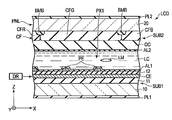
- FIG. 4 is a sectional view of the liquid crystal element LCD including the first pixel PX1 shown in FIG.
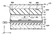
- FIG. 5 is a cross-sectional view of the liquid crystal element LCD including the second pixel PX2 shown in FIG.
- FIG. 6 is a block diagram showing a configuration example for controlling the liquid crystal panel PNL.
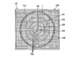
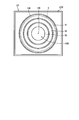
- FIG. 7 is a plan view showing one configuration example of the liquid crystal element LCD superimposed on the camera 1.
- FIG. 1 is an exploded perspective view showing one configuration example of the display device DSP of the present embodiment.
- FIG. 2 is a sectional view including the display device DSP and the camera 1 shown in FIG.
- FIG. 3 is a plan view showing a configuration example of the liquid crystal panel
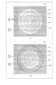
- FIG. 8 is a plan view showing a control example of the liquid crystal element LCD shown in FIG.
- FIG. 9 is a plan view showing another control example of the liquid crystal element LCD shown in FIG.
- FIG. 10 is a flowchart for explaining a control example of the liquid crystal element LCD of the present embodiment.
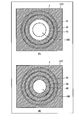
- FIG. 11 is a plan view showing another configuration example of the liquid crystal element LCD superimposed on the camera 1.
- FIG. 12 is a cross-sectional view of the liquid crystal element LCD shown in FIG.
- FIG. 13 is a plan view showing a control example of the liquid crystal element LCD shown in FIG.
- FIG. 14 is a plan view showing another control example of the liquid crystal element LCD shown in FIG.
- FIG. 15 is a diagram illustrating a display example of a pattern displayed outside the camera 1 on the liquid crystal element LCD of the present embodiment.
- FIG. 16 is a flowchart for explaining a control example of the liquid crystal element LCD of the present embodiment.
- FIG. 17 is a diagram illustrating a display example on the display
- FIG. 1 is an exploded perspective view showing one configuration example of the display device DSP of the present embodiment.
- the first direction X, the second direction Y, and the third direction Z are orthogonal to each other, but may intersect at an angle other than 90 degrees.
- the first direction X and the second direction Y correspond to directions parallel to the main surface of the substrate constituting the display device DSP, and the third direction Z corresponds to the thickness direction of the display device DSP.
- the display device DSP includes a first polarizing plate PL1 and a second polarizing plate PL2, a liquid crystal panel PNL, an optical sheet OS, a light guide plate LG, a light source EM, and a reflection sheet RS.
- the reflection sheet RS, the light guide plate LG, the optical sheet OS, the first polarizing plate PL1, the liquid crystal panel PNL, and the second polarizing plate PL2 are arranged in this order along the third direction Z.
- the plurality of light sources EM are arranged at intervals along the first direction X. At least the light source EM and the light guide plate LG constitute a planar light source ALS that illuminates the liquid crystal panel PNL.
- the planar light source ALS may further include an optical sheet OS and a reflection sheet RS.
- the first polarizing plate PL1, the second polarizing plate PL2, and the liquid crystal panel PNL constitute a liquid crystal element LCD having an optical switching function for light traveling in the third direction Z.
- Such a liquid crystal element LCD exhibits a function of transmitting or blocking light for each region in the XY plane defined by the first direction X and the second direction Y.
- the electronic device 100 incorporating such a display device DSP includes the camera 1.
- the liquid crystal panel PNL is formed in a flat plate shape parallel to the XY plane.
- the liquid crystal panel PNL is located between the first polarizing plate PL1 and the second polarizing plate PL2.
- the liquid crystal panel PNL includes a display section DA for displaying an image, and a frame-shaped non-display section NDA surrounding the display section DA.
- the liquid crystal panel PNL overlaps the camera 1 in the third direction Z, and in particular, the display unit DA overlaps the camera 1.
- the liquid crystal panel PNL uses a display mode using a horizontal electric field along the main surface of the substrate and a vertical electric field along a normal to the main surface of the substrate.
- Display mode a display mode using an inclined electric field inclined in an oblique direction with respect to the main surface of the substrate, and further, any of the above-described horizontal electric field, vertical electric field, and a display mode using an appropriately combined inclined electric field A configuration may be provided.
- the substrate main surface is a surface parallel to the XY plane.
- the first polarizing plate PL1 and the second polarizing plate PL2 overlap at least the display section DA with respect to the liquid crystal panel PNL.
- the first polarizing plate PL1 and the second polarizing plate PL2 overlap the camera 1 in the third direction Z.
- the light guide plate LG includes a first side surface SA facing the light source EM, a second side surface SB opposite to the first side surface SA, a main surface SC facing the liquid crystal panel PNL, and a main surface opposite to the main surface SC. SD and a first through hole TH1.
- the first through hole TH1 is located between the first side surface SA and the second side surface SB in the second direction Y, and is closer to the second side surface SB than the first side surface SA.
- the camera 1 overlaps the first through hole TH1 in the third direction Z.
- the plurality of optical sheets OS are located between the light guide plate LG and the liquid crystal panel PNL, and face the main surface SC.
- Each of the optical sheets OS has a second through hole TH2 that overlaps the first through hole TH1.
- the optical sheet OS is, for example, a prism sheet or a diffusion sheet.
- the reflection sheet RS faces the main surface SD. That is, the light guide plate LG is located between the reflection sheet RS and the optical sheet OS.
- the reflection sheet RS has a third through hole TH3 overlapping the first through hole TH1.
- the third through-hole TH3, the first through-hole TH1, and the second through-hole TH2 are arranged in this order along the third direction Z and are provided on the same straight line.
- the reflection sheet RS may be fixed to a frame made of metal, for example. In that case, a through-hole overlapping the first through-hole TH1 may be provided in the frame.
- the light source EM is, for example, a light emitting diode (LED) and emits white illumination light.
- the illumination light emitted from the light source EM enters from the first side surface SA and travels along the direction of the arrow indicating the second direction Y. Then, the illumination light guided by the light guide plate LG is emitted from the main surface SC toward the liquid crystal panel PNL, and illuminates the liquid crystal panel PNL.
- the liquid crystal panel PNL, the first polarizing plate PL1, and the second polarizing plate PL2 display an image in the display section DA by selectively transmitting illumination light.
- FIG. 2 is a cross-sectional view including the display device DSP and the camera 1 shown in FIG.
- the liquid crystal panel PNL includes a first substrate SUB1, a second substrate SUB2, a liquid crystal layer LC, and a seal SE.
- the seal SE is located in the non-display portion NDA, and bonds the first substrate SUB1 and the second substrate SUB2 and seals the liquid crystal layer LC.
- the first substrate SUB1 includes a first insulating substrate 10 and an alignment film AL1.
- the second substrate SUB2 includes a second insulating substrate 20, a color filter CF, a light shielding layer BMA, a transparent layer OC, and an alignment film AL2.
- the first insulating substrate 10 and the second insulating substrate 20 are transparent substrates such as a glass substrate and a flexible resin substrate.
- the alignment films AL1 and AL2 are in contact with the liquid crystal layer LC.
- the color filter CF, the light shielding layer BMA, and the transparent layer OC are located between the second insulating substrate 20 and the liquid crystal layer LC.
- the light shielding layer BMA is located in the non-display area NDA.
- a boundary B between the display section DA and the non-display section NDA corresponds to an inner end of the light shielding layer BMA.
- the seal SE is provided at a position overlapping the light shielding layer BMA.
- the color filter CF includes red, green, and blue color filters.
- the transparent layer OC covers the color filter CF and the light shielding layer BMA.
- the transparent layer OC is, for example, a transparent organic insulating film.
- the display unit DA has an area A1 where the color filters CF are arranged and an area A2 where the color filters CF are not arranged.
- the transparent layer OC is disposed over the region A1 and the region A2, and is in contact with the color filter CF in the region A1, and is in contact with the second insulating substrate 20 in the region A2. Focusing on the positional relationship between the camera 1 and the display unit DA, the camera 1 is superimposed on the area A2. That is, the color filter CF is not superimposed on the camera 1.
- the first polarizing plate PL1 is bonded to the first insulating substrate 10.
- the second polarizing plate PL2 is bonded to the second insulating substrate 20.
- the first polarizing plate PL1 and the second polarizing plate PL2 are arranged over the area A1 and the area A2, and are superimposed on the camera 1.
- the liquid crystal element LCD may include a retardation plate, a scattering layer, an anti-reflection layer, and the like as necessary.
- the second polarizing plate PL2 or the first polarizing plate PL1 may include a super birefringent film.
- a super birefringent film depolarizes transmitted light (natural light) when linearly polarized light is incident, so that even if a subject includes a substance that emits polarized light, it can be photographed without a sense of incongruity.
- a liquid crystal display device or the like is reflected on a subject of the camera 1
- the subject is the first polarizing plate PL1 and the second polarizing plate PL2 and the subject.
- the brightness of the liquid crystal display device of the subject incident on the camera 1 changes depending on the angle relationship with the polarizing plate of the liquid crystal display device, which may cause a sense of incongruity during shooting.
- the second polarizing plate PL2 or the first polarizing plate PL1 with the super-birefringent film, it is possible to suppress a change in brightness that causes a sense of incongruity.
- the film exhibiting super birefringence for example, Cosmoshine (registered trademark) of Toyobo Co., Ltd. is preferably used.
- the term “super-birefringence” means that the in-plane retardation for light in the visible region, for example, 550 nm, is 800 nm or more.
- the first through-hole TH1, the second through-hole TH2, and the third through-hole TH3 overlap with each other to form a space SP opened below the liquid crystal panel PNL.
- the camera 1 is provided in a space SP formed by the first through hole TH1 and the like.
- the camera 1 includes, for example, an optical system 2 including at least one lens, an image sensor (imaging element) 3, and a case 4.
- the case 4 houses the optical system 2 and the image sensor 3.
- the optical system 2 is located between the liquid crystal panel PNL and the image sensor 3, and the camera 1 can receive light via the liquid crystal panel PNL.
- the camera 1 is electrically connected to the wiring board F.
- the camera 1 does not necessarily need to be provided in the first through hole TH1, and may be provided outside the space SP.
- the camera 1 only needs to be provided at a position overlapping the first through hole TH1 in the third direction Z.
- an example has been described in which the camera 1 that overlaps the first through hole TH1 is provided.
- a light receiving element that receives light irradiated through the first through hole TH1 and the optical system 2 and outputs an electric signal is provided. It may overlap with the first through hole TH1.
- the camera 1 is superimposed on the display section DA of the liquid crystal panel PNL. Therefore, there is no need to provide a space for installing the camera 1 in the non-display portion NDA. Therefore, as compared with the case where the camera 1 is superimposed on the non-display portion NDA, or the case where the camera 1 and the liquid crystal panel PNL are arranged side by side in the second direction Y without the camera 1 being superimposed on the display portion DA. Thus, the frame width of the non-display portion NDA can be reduced.
- the color filter CF is provided on the second substrate SUB2, but may be provided on the first substrate SUB1.
- FIG. 3 is a plan view showing a configuration example of the liquid crystal panel PNL shown in FIG.
- the liquid crystal layer LC and the seal SE are indicated by different oblique lines.
- the display section DA is a substantially rectangular area that does not include the notch, and is located inside the area surrounded by the seal SE.
- the area A1 and the area A2 are arranged in the second direction Y.
- the area A1 is an area where the color filters CF are arranged
- the area A2 is an area where the color filters CF are not arranged. That is, the area A2 is a monochrome display area, and corresponds to an area where a stepwise display from white (or transparent) display to black display is possible. That is, in the area A2, halftone (gray) display is also possible.
- the area A1 corresponds to an area where color display is possible.
- the area A2 includes an area overlapping with the camera 1 and extends in the first direction X. Note that the area A2 may be only an area that overlaps with the camera 1, and in this case, the area A1 is extended to an area around the camera 1.
- the liquid crystal panel PNL includes pixels PX arranged in a matrix in the first direction X and the second direction Y in the regions A1 and A2 of the display unit DA.
- the first pixel PX1 included in the area A1 does not overlap with the camera 1.
- the area A2 includes a second pixel PX2 to be superimposed on the camera 1.
- Each pixel PX in the display section DA has the same circuit configuration.
- the outline of the camera 1 is indicated by a dotted line, and the second pixel PX2 superimposed on the camera 1 is indicated.
- the second pixel PX2 overlaps the optical system 2 including the lens of the camera 1 in a plan view.
- the pixel PX overlapping the case 4 of the camera 1 may be included in the second pixel PX2.
- each pixel PX includes a switching element SW, a pixel electrode PE, a common electrode CE, a liquid crystal layer LC, and the like.
- the switching element SW is composed of, for example, a thin film transistor (TFT), and is electrically connected to the scanning line G and the signal line S.
- the pixel electrode PE is electrically connected to the switching element SW.
- Each of the pixel electrodes PE faces the common electrode CE, and drives the liquid crystal layer LC by an electric field generated between the pixel electrode PE and the common electrode CE.
- the capacitor CS is formed, for example, between an electrode having the same potential as the common electrode CE and between an electrode having the same potential as the pixel electrode PE.
- the wiring substrate 5 is electrically connected to the extension Ex of the first substrate SUB1.
- the IC chip 6 is electrically connected to the wiring board 5. Note that the IC chip 6 may be electrically connected to the extension Ex.
- the IC chip 6 includes, for example, a display driver that outputs a signal necessary for image display.
- the wiring board 5 is a bendable flexible printed circuit board.
- FIG. 4 is a cross-sectional view of the liquid crystal element LCD including the first pixel PX1 shown in FIG.
- a liquid crystal element LCD including a liquid crystal panel PNL corresponding to a display mode using a horizontal electric field between the first polarizing plate PL1 and the second polarizing plate PL2 will be described.
- the first substrate SUB1 includes insulating films 11 and 12, a common electrode CE, and a pixel electrode PE between the first insulating substrate 10 and the alignment film AL1.
- the common electrode CE is located on the insulating film 11 and is covered by the insulating film 12.
- the pixel electrode PE is located on the insulating film 12 and is covered by the alignment film AL1.
- the pixel electrode PE is opposed to the common electrode CE via the insulating film 12.
- the common electrode CE and the pixel electrode PE are formed of a transparent conductive material such as indium tin oxide (ITO) or indium zinc oxide (IZO).
- the insulating film 11 includes an inorganic insulating film and an organic insulating film.
- the insulating film 12 is, for example, an inorganic insulating film such as silicon nitride.
- the light shielding layer BMB is formed integrally with the light shielding layer BMA of the non-display portion NDA described with reference to FIG.
- the color filter CF includes a red color filter CFR, a green color filter CFG, and a blue color filter CFB.
- the color filter CFG faces the pixel electrode PE.
- the other color filters CFR and CFB also face other pixel electrodes PE (not shown).
- the driving unit DR that drives the liquid crystal element LCD includes, for example, a scanning line driving circuit electrically connected to the scanning line G and a signal line driving circuit electrically connected to the signal line S illustrated in FIG. Contains.
- the drive section DR outputs a signal necessary for image display to each pixel PX of the display section DA, and controls the transmittance of the liquid crystal element LCD.
- the transmittance of the liquid crystal element LCD is controlled according to the magnitude of the voltage applied to the liquid crystal layer LC. For example, in the off state where no voltage is applied to the liquid crystal layer LC in the first pixel PX1, the liquid crystal molecules LM included in the liquid crystal layer LC are initially aligned in a predetermined direction between the alignment films AL1 and AL2. .
- the liquid crystal element LCD displays black in the first pixel PX1 in the off state.
- the ON state in which a voltage is applied to the liquid crystal layer LC, the liquid crystal molecules LM are oriented in a direction different from the initial orientation direction due to an electric field formed between the pixel electrode PE and the common electrode CE. Is controlled by the electric field. In such an ON state, a part of the light guided to the first pixel PX1 passes through the first polarizing plate PL1 and the second polarizing plate PL2.
- the liquid crystal element LCD displays a color corresponding to the color filter CF in the first pixel PX1 in the ON state.
- the above example corresponds to a so-called normally black mode in which black is displayed in an off state, but a normally white mode in which black is displayed in an on state (white is displayed in an off state) may be applied.
- FIG. 5 is a cross-sectional view of the liquid crystal element LCD including the second pixel PX2 shown in FIG.
- the second pixel PX2 is different from the first pixel PX1 shown in FIG. 4 in that the second substrate SUB2 does not include the color filter CF. That is, the transparent layer OC is in contact with the second insulating substrate 20 immediately above the pixel electrode PE.
- a transparent resin layer may be provided between the transparent layer OC and the second insulating substrate 20.
- the transmittance of the second pixel PX2 of the liquid crystal element LCD is controlled by the driving unit DR, similarly to the first pixel PX1. That is, the liquid crystal element LCD has the minimum transmittance and displays black in the second pixel PX2 in the off state where no voltage is applied to the liquid crystal layer LC, similarly to the first pixel PX1. That is, the liquid crystal element LCD exhibits a light blocking function in the second pixel PX2.
- the voltage is applied to the liquid crystal layer LC, part of the light guided to the second pixel PX2 passes through the first polarizing plate PL1 and the second polarizing plate PL2.
- the liquid crystal element LCD displays white or is in a transparent state when the second pixel PX2 in the on state has the maximum transmittance. Further, as described above, the liquid crystal element LCD is controlled to have an intermediate transmittance between the minimum transmittance and the maximum transmittance, and may display gray. That is, the liquid crystal element LCD exhibits a light transmitting function in the second pixel PX2.
- the light shielding layer BMB is formed in the region A1 and the region A2. However, the width of the light shielding layer BMB in the region A2 may be smaller than the width of the light shielding layer BMB in the region A1. Further, the light shielding layer BMB may not be provided in the region A2.
- the reason why the width of the light-shielding layer BMB is reduced or the light-shielding layer BMB is not provided may be only one of the first direction X and the second direction Y, and is bidirectional in the first direction X and the second direction Y. Is also good.
- FIG. 6 is a block diagram showing an example of a configuration for controlling the liquid crystal panel PNL.
- the electronic device 100 includes a main controller 110, a memory 120, an optical sensor 130, and a mode switch 140, in addition to the camera 1 and the liquid crystal panel PNL.
- the memory 120 stores various data and various programs for controlling the electronic device 100.
- the optical sensor 130 measures the brightness around the electronic device 100, and outputs a measurement result to the main controller 110.
- the optical sensor 130 includes, for example, a light receiving element such as a photodiode or a phototransistor. In one example, the optical sensor 130 is an illuminometer that measures illuminance as brightness.
- the mode switch 140 is a user interface operated by a user, and receives a setting input of a desired mode.
- the main controller 110 implements various functions by a program stored in the memory 120. For example, the main controller 110 controls the driving unit DR of the liquid crystal panel PNL based on a measurement result from the optical sensor 130 or a setting
- FIG. 7 is a plan view showing one configuration example of the liquid crystal element LCD superimposed on the camera 1.
- the liquid crystal element LCD has, for example, four regions A21 to A24 as regions to be superimposed on the camera 1.
- the regions A21 to A23 are each formed in a ring shape.
- the region A24 is formed in a substantially circular shape.
- the area A22 is adjacent to the inside of the area A21
- the area A23 is adjacent to the inside of the area A22
- the area A24 is adjacent to the inside of the area A23.
- the four regions A21 to A24 are formed substantially isotropically about the optical axis OX of the camera 1. Note that the liquid crystal element LCD may be divided into five or more regions or three or less regions as a region to be superimposed on the camera 1.
- the regions A21 to A23 are not limited to a ring shape, and the regions A21 to A24 may have a stripe shape or the like.
- the area A21 of the present invention is made to correspond to the shape of the area with the strongest backlight, and the area A24 is adjusted to the shape of the subject. Shapes are also possible.
- the liquid crystal element LCD has an area A30 outside the camera 1 and surrounding the area A21. In these areas A21 to A24 and area A30, the second pixels PX2 shown in FIG.
- the regions A21 to A23 corresponds to the first region
- at least one of the regions A22 to A24 inside the first region corresponds to the second region
- the region A30 corresponds to the first region. This corresponds to three regions.
- the camera 1 is provided in the first through hole TH1 of the light guide plate LG, and all four regions A21 to A24 overlap the first through hole TH1.
- the region A30 overlaps with the light guide plate LG.
- Such a liquid crystal element LCD can function as a diaphragm for adjusting the amount of light incident on the camera 1 by transmitting or blocking light for each area.
- FIG. 8 is a plan view showing a control example of the liquid crystal element LCD shown in FIG. FIG. 8A is a diagram for explaining the first aperture mode.
- the liquid crystal element LCD in the first aperture mode transmits light in the regions A21 to A24.
- the second pixel PX2 in each of the regions A21 to A24 is in the ON state described with reference to FIG.
- the transmittance of the second pixel PX2 does not need to be the maximum transmittance, but may be an intermediate transmittance. Therefore, when the liquid crystal element LCD is set to the first aperture mode, the light transmitted through the regions A21 to A24 is received by the camera 1.
- the second pixel PX2 in the area A30 is in the off state, and the liquid crystal element LCD blocks light in the area A30.
- the liquid crystal element LCD may transmit light in the region A30.
- the second pixel PX2 that transmits light is represented by white
- the second pixel PX2 that shields light is represented by gray.
- FIG. 8B is a diagram for explaining the second aperture mode.
- the liquid crystal element LCD in the second aperture mode shields light in the region A21 and transmits light in the regions A22 to A24.
- the second pixel PX2 in the region A21 is off, and the second pixels PX2 in each of the regions A22 to A24 are on.
- the second pixel PX2 in the region A30 is also in the off state, and the region A30 is shielded from light. Therefore, when the liquid crystal element LCD is set to the second aperture mode, the light transmitted through the regions A22 to A24 is received by the camera 1.
- the total number of transmissive second pixels PX2 is greater in the second aperture mode than in the first aperture mode. Few. Further, among the areas superimposed on the camera 1, the total area of the light transmitting areas is smaller in the second aperture mode than in the first aperture mode.
- the case where light is shielded in the area A21 has been described as the second aperture mode, but it is sufficient that the transmitted light quantity in the area A21 is smaller than the transmitted light quantity in the areas A22 to A24. In other words, the transmittance of the region A21 only needs to be set lower than the transmittance of the regions A22 to A24.
- FIG. 9 is a plan view showing another control example of the liquid crystal element LCD shown in FIG.
- FIG. 9A is a diagram for explaining the third aperture mode.
- the liquid crystal element LCD in the third aperture mode blocks light in the regions A21 and A22 and transmits light in the regions A23 to A24.
- FIG. 9B is a diagram for explaining the fourth aperture mode.
- the liquid crystal element LCD in the fourth aperture mode blocks light in the regions A21 to A23 and transmits light in the region A24.
- FIG. 10 is a flowchart for explaining a control example of the liquid crystal element LCD of the present embodiment.
- the main controller 110 determines whether or not the brightness of the outside light is equal to or lower than level 1 based on the measurement result by the optical sensor 130 (step ST1).
- the main controller 110 controls the driving unit DR so as to realize the first opening mode shown in FIG. 8A (step ST2).
- the liquid crystal panel PNL is driven by the driving unit DR, and the liquid crystal element LCD transmits light in the areas A21 to A24. Therefore, even in a dark place where the brightness is determined to be level 1 or less, more light can be taken into the camera 1.
- the main controller 110 determines whether the brightness is lower than level 2 (step ST3). Similarly, when the main controller 110 determines that the brightness is equal to or lower than the level 2 (ST3, YES), the main controller 110 controls to realize the second aperture mode shown in FIG. 8B ( (Step ST4) If it is determined that the brightness is equal to or lower than the level 3 (ST5, YES), control is performed so as to realize the third aperture mode shown in FIG. 9A (step ST6). If it is determined that the brightness is higher than level 3 (ST5, NO), control is performed to realize the fourth aperture mode shown in FIG. 9B (step ST7). As described above, in a light place where the brightness is determined to be higher than the level 1, the amount of light to be taken into the camera 1 can be appropriately adjusted according to the brightness.
- the amount of light to be taken into the camera 1 can be adjusted by the liquid crystal element LCD superimposed on the camera 1 in accordance with the surrounding brightness, and the liquid crystal element LCD is sharp even in a bright place or a dark place. You can take pictures.
- the aperture mode is controlled based on the measurement result by the optical sensor 130 .
- the aperture mode may be controlled based on a setting input by the user via the mode switch 140.
- FIG. 11 is a plan view showing another configuration example of the liquid crystal element LCD superimposed on the camera 1.
- the liquid crystal element LCD includes, for example, three electrodes 51 to 53 in a region overlapping with the camera 1.
- Each of the electrodes 51 to 53 is a transparent electrode formed in a ring shape.
- the electrode 52 is adjacent to the inside of the electrode 51
- the electrode 53 is adjacent to the inside of the electrode 52
- the area A50 inside the electrode 53 is formed in a substantially circular shape.
- the three electrodes 51 to 53 are formed substantially isotropically about the optical axis OX of the camera 1.
- the liquid crystal element LCD may include four or more transparent electrodes or two or less transparent electrodes in a region overlapping the camera 1.
- the electrodes 51 to 53 and the region A50 all overlap the first through hole TH1.
- FIG. 11 illustrates only the three electrodes 51 to 53, but a pixel similar to the pixel PX illustrated in FIG. 3 is formed in a region other than the electrodes 51 to 53. Pixels other than 53 are called pixels PX).
- the pixels PX included in the region A2 shown in FIG. 3 may be pixels capable of performing color display except for the electrodes 51 to 53.
- FIG. 12 is a cross-sectional view of the liquid crystal element LCD shown in FIG.
- the first substrate SUB1 includes electrodes 51 to 53 between the first insulating substrate 10 and the alignment film AL1. Each of the electrodes 51 to 53 is electrically connected to the drive unit DR via the switching elements SW1 to SW3.
- the second substrate SUB2 includes an electrode 54 between the second insulating substrate 20 and the alignment film AL2.
- the electrode 54 is a transparent electrode and faces each of the electrodes 51 to 53.
- the electrode 54 is electrically connected to the driving unit DR.
- the liquid crystal layer LC located between the alignment films AL1 and AL2 includes liquid crystal molecules LM that are twist-aligned in an off state where no voltage is applied.
- the state in which the driving unit DR applies a potential different from that of the electrode 54 to each of the electrodes 51 to 53 via the switching elements SW1 to SW corresponds to an ON state in which a voltage is applied to the liquid crystal layer LC.
- the liquid crystal molecules LM are oriented substantially perpendicular to the first substrate SUB1 and the second substrate SUB2.
- the polarization axis AX1 of the first polarizing plate PL1 and the polarization axis AX2 of the second polarizing plate PL2 are orthogonal to each other.
- Such a liquid crystal element LCD transmits light in an off state where no voltage is applied to the liquid crystal layer LC, and blocks light in an on state where a voltage is applied to the liquid crystal layer LC. Further, the liquid crystal element LCD transmits light because no voltage is applied to the liquid crystal layer LC in the region A50.
- the electrodes 51 to 53 are larger than the transparent electrode (pixel electrode) of the pixel PX (area ratio: several times to several tens times). Therefore, when the switching elements SW1 to SW3 are connected to wirings (such as the scanning lines G and the signal lines S illustrated in FIG. 3) that supply signals to the pixels PX, among the signal lines connected to the driving unit DR, the electrodes 51 to SW3 are used.
- a difference occurs in the load (capacity of the signal line) of the driving unit DR between the signal line connected to 53 and the signal line not connected to the electrodes 51 to 53. If there is a difference between the capacitances of the signal lines, a problem such as loss of display uniformity occurs. Therefore, as shown in FIG. 12, a wiring connected to the switching elements SW1 to SW3 supplies a signal to the pixel PX. By forming it in a peripheral region outside the display region separately from the wiring, it is possible to avoid a problem caused by a difference in capacitance of the signal line. Further, as shown in FIG. 12, the switching elements SW1 to SW3 are also formed in the non-display section NDA outside the display section DA so as not to block the light incident on the camera 1.
- the switching elements SW1 to SW3 can be formed not at the non-display portion NDA but at a position overlapping the camera 1 or at the display portion DA. However, in order to reduce light that is blocked, the switching elements SW1 to SW3 are formed at a lower density than the switching elements SW formed in the pixels PX. Since the electrodes 51 to 53 are larger than the pixel electrodes of the pixel PX, the switching elements SW1 to SW3 may be larger (the channel width is longer) than the switching elements SW.
- FIG. 13 is a plan view showing a control example of the liquid crystal element LCD shown in FIG.
- FIG. 13A is a diagram for explaining the first aperture mode.
- the liquid crystal element LCD in the first aperture mode transmits light in a region overlapping with the electrodes 51 to 53 and a region A50.
- no voltage is applied to the liquid crystal layer LC illustrated in FIG. Therefore, when the liquid crystal element LCD is set to the first aperture mode, the camera 1 receives light transmitted through the electrodes 51 to 53 and the area A50.
- FIG. 13B is a diagram for explaining the second aperture mode.
- the liquid crystal element LCD in the second aperture mode blocks light in a region overlapping the electrode 51 and transmits light in a region overlapping the electrodes 52 and 53 and a region A50. In a region overlapping with the electrode 51, a voltage is applied to the liquid crystal layer LC. Therefore, when the liquid crystal element LCD is set to the second aperture mode, light transmitted through the electrodes 52 and 53 and the area A50 is received by the camera 1.
- FIG. 14 is a plan view showing another control example of the liquid crystal element LCD shown in FIG.
- FIG. 14A is a diagram for explaining the third aperture mode.
- the liquid crystal element LCD in the third aperture mode blocks light in a region overlapping the electrodes 51 and 52, and transmits light in a region overlapping the electrode 53 and the region 50.
- FIG. 14B is a diagram for explaining the fourth aperture mode.
- the liquid crystal element LCD in the fourth aperture mode blocks light in a region overlapping the electrodes 51 to 53 and transmits light in a region A50.
- the control example described with reference to FIG. 10 is applicable. Further, the opening mode may be controlled based on a setting input by the user via the mode switch 140. Therefore, the same effect as in the above configuration example can be obtained.
- FIG. 15 is a diagram illustrating a display example of a pattern displayed outside the camera 1 on the liquid crystal element LCD of the present embodiment.
- the various patterns described here are displayed, for example, in an area A30 shown in FIG.
- FIG. 15A shows a first pattern PT1 displayed corresponding to the first opening mode
- FIG. 15B shows a second pattern PT2 displayed corresponding to the second opening mode
- FIG. 15C shows a third pattern PT3 displayed corresponding to the third opening mode
- FIG. 15D shows a fourth pattern PT4 displayed corresponding to the fourth opening mode.
- Each of the first to fourth patterns PT1 to PT4 is an annular pattern.
- the first to fourth patterns PT1 to PT4 are all displayed by a plurality of blades surrounding the camera 1, but are not limited thereto, and may be displayed by a simple donut-shaped annular pattern. May be displayed in a spiral annular pattern, or may be displayed in other patterns.
- Opening patterns AP1 to AP4 are displayed inside each of the first to fourth patterns PT1 to PT4.
- the opening patterns AP1 to AP4 may be displayed in a circular pattern or in a polygonal pattern.
- the area of the opening pattern AP2 is smaller than the area of the opening pattern AP1
- the area of the opening pattern AP3 is smaller than the area of the opening pattern AP2
- the area of the opening pattern AP4 is smaller than the area of the opening pattern AP3.
- the first pattern PT1 is displayed with a different gradation from the inside and outside.
- the first pattern PT1 is displayed in black or gray
- the outside of the first pattern PT1 is displayed in white
- the opening pattern AP1 inside the first pattern PT1 is displayed in white.
- the other second to fourth patterns PT2 to PT4 are displayed in the same manner as the first pattern PT1.
- annular patterns Although four annular patterns are shown here, the present invention is not limited to a mode in which these four annular patterns are displayed in a stepwise manner, and a display mode in which the area of the opening pattern continuously changes is applied. May be done.
- FIG. 16 is a flowchart for explaining a control example of the liquid crystal element LCD of the present embodiment.
- the main controller 110 determines that the brightness of the outside light is equal to or lower than the level 1 based on the measurement result by the optical sensor 130 (ST11, YES)
- the main controller 110 switches the first aperture mode shown in FIG. Control is performed so as to realize (step ST12), and control is performed so as to display the first pattern PT1 and the opening pattern AP1 shown in FIG. 15A (step ST13).
- the main controller 110 controls to realize the second aperture mode shown in FIG.
- step ST15 Further, control is performed so as to display the second pattern PT2 and the opening pattern AP2 shown in FIG. 15B (step ST16). If the main controller 110 determines that the brightness is equal to or lower than the level 3 (ST17, YES), the main controller 110 controls to realize the third aperture mode shown in FIG. 9A (step ST18), Further, control is performed so as to display the third pattern PT3 and the opening pattern AP3 shown in FIG. 15C (step ST19). If the main controller 110 determines that the brightness is higher than the level 3 (ST17, NO), it controls to realize the fourth aperture mode shown in FIG. 9B (step ST20). Control is performed so as to display the fourth pattern PT4 and the opening pattern AP4 shown in FIG. 15D (step ST21).
- the aperture mode when the aperture mode is automatically controlled based on the brightness measured by the optical sensor 130, the user can be visually notified of the set aperture mode. .
- the area of the liquid crystal element LCD superimposed on the camera 1 is small, and it may be difficult to directly view the set aperture mode.
- a pattern corresponding to the opening mode is displayed outside the region overlapping with the camera 1, so that the user can easily recognize the opening mode.
- the same effect can be obtained by displaying a pattern corresponding to the opening mode.
- FIG. 17 is a diagram illustrating a display example on the display device DSP of the present embodiment.
- FIG. 17A corresponds to a display example in a shooting mode in which the camera 1 shoots.
- the shooting mode here is, for example, a mode in which the user of the electronic device 100 shoots himself as a subject.
- an area overlapping with the camera 1 is set to, for example, one of the opening modes shown in FIGS. 8 and 9, and an annular pattern PT corresponding to the opening mode is provided outside the camera 1.
- the opening pattern AP is displayed inside the annular pattern PT.
- the annular pattern PT is displayed, for example, in monochrome.
- FIG. 17B corresponds to a display example when the camera 1 is not used.
- characters such as numerals, characters, symbols, and marks are displayed in monochrome.
- a character can be displayed even at a position where the character is superimposed on the camera 1.
- a still image, a moving image, and the like are displayed in color.
- the color filter CF is arranged in the area A1
- the color filter CF is not arranged in the area A2
- color display may be realized in the area A2 by using a field sequential method. Therefore, even if the color filter CF is not arranged in the area A2, the annular pattern PT can be displayed in color.
- a display device capable of narrowing a frame
- an electronic device incorporating the display device and a program.
- an electronic device capable of taking a clear picture can be provided.
Landscapes
- Physics & Mathematics (AREA)
- Nonlinear Science (AREA)
- General Physics & Mathematics (AREA)
- Chemical & Material Sciences (AREA)
- Optics & Photonics (AREA)
- Crystallography & Structural Chemistry (AREA)
- Mathematical Physics (AREA)
- Engineering & Computer Science (AREA)
- Liquid Crystal (AREA)
- Computer Hardware Design (AREA)
- Theoretical Computer Science (AREA)
- Signal Processing (AREA)
- Multimedia (AREA)
- Exposure Control For Cameras (AREA)
- Shutters For Cameras (AREA)
Abstract
狭額縁化が可能な電子機器を提供する。 カメラと、第1偏光板と、第2偏光板と、前記第1偏光板と前記第2偏光板との間に位置する液晶パネルと、前記液晶パネルを制御するコントローラと、を備え、前記液晶パネルは、前記カメラに重畳する第1領域及び第2領域を有し、前記コントローラは、前記第1領域及び前記第2領域で透光する第1開口モードと、前記第1領域の透過光量を前記第2領域の透過光量よりも低減する第2開口モードと、を制御する、電子機器。
Description
本発明の実施形態は、表示装置、表示装置を組み込んだ電子機器、及び、プログラムに関する。
近年、表示部及びカメラを同一面側に備えたスマートフォン等の電子機器が広く実用化されている。このような電子機器では、カメラが表示部の外側に設けられており、カメラを設置するためのスペースを確保する一方で、表示部の外側の額縁幅を縮小する要望が高まっている。
また、鮮明な写真を撮影可能とすることが要望されている。
また、鮮明な写真を撮影可能とすることが要望されている。
本実施形態の目的は、狭額縁化が可能な表示装置、表示装置を組み込んだ電子機器、及び、プログラムを提供することにある。
本実施形態によれば、
カメラと、第1偏光板と、第2偏光板と、前記第1偏光板と前記第2偏光板との間に位置する液晶パネルと、前記液晶パネルを制御するコントローラと、を備え、前記液晶パネルは、前記カメラに重畳する第1領域及び第2領域を有し、前記コントローラは、前記第1領域及び前記第2領域で透光する第1開口モードと、前記第1領域の透過光量を前記第2領域の透過光量よりも低減する第2開口モードと、を制御する、電子機器が提供される。
本実施形態によれば、
カメラの前方に配置される表示装置であって、第1偏光板と、第2偏光板と、前記第1偏光板と前記第2偏光板との間に位置する液晶パネルと、を備え、前記液晶パネルは、前記カメラに重畳する第1領域及び第2領域を有し、第1開口モードにおいて、前記第1領域及び前記第2領域で透光し、第2開口モードにおいて、前記第1領域の透過光量を前記第2領域の透過光量よりも低減する、表示装置が提供される。
本実施形態によれば、
カメラと、前記カメラに重畳する第1領域及び第2領域を有する液晶素子と、を制御するコンピュータに、前記第1領域及び前記第2領域で透光する第1開口モードと、前記第1領域の透過光量を前記第2領域の透過光量よりも低減する第2開口モードと、を実現させるためのプログラムが提供される。
カメラと、第1偏光板と、第2偏光板と、前記第1偏光板と前記第2偏光板との間に位置する液晶パネルと、前記液晶パネルを制御するコントローラと、を備え、前記液晶パネルは、前記カメラに重畳する第1領域及び第2領域を有し、前記コントローラは、前記第1領域及び前記第2領域で透光する第1開口モードと、前記第1領域の透過光量を前記第2領域の透過光量よりも低減する第2開口モードと、を制御する、電子機器が提供される。
本実施形態によれば、
カメラの前方に配置される表示装置であって、第1偏光板と、第2偏光板と、前記第1偏光板と前記第2偏光板との間に位置する液晶パネルと、を備え、前記液晶パネルは、前記カメラに重畳する第1領域及び第2領域を有し、第1開口モードにおいて、前記第1領域及び前記第2領域で透光し、第2開口モードにおいて、前記第1領域の透過光量を前記第2領域の透過光量よりも低減する、表示装置が提供される。
本実施形態によれば、
カメラと、前記カメラに重畳する第1領域及び第2領域を有する液晶素子と、を制御するコンピュータに、前記第1領域及び前記第2領域で透光する第1開口モードと、前記第1領域の透過光量を前記第2領域の透過光量よりも低減する第2開口モードと、を実現させるためのプログラムが提供される。
以下、本実施形態について、図面を参照しながら説明する。なお、開示はあくまで一例に過ぎず、当業者において、発明の主旨を保っての適宜変更について容易に想到し得るものについては、当然に本発明の範囲に含有されるものである。また、図面は、説明をより明確にするため、実際の態様に比べて、各部の幅、厚さ、形状等について模式的に表される場合があるが、あくまで一例であって、本発明の解釈を限定するものではない。また、本明細書と各図において、既出の図に関して前述したものと同一又は類似した機能を発揮する構成要素には同一の参照符号を付し、重複する詳細な説明を適宜省略することがある。
図1は、本実施形態の表示装置DSPの一構成例を示す分解斜視図である。一例では、第1方向X、第2方向Y、及び、第3方向Zは、互いに直交しているが、90度以外の角度で交差していてもよい。第1方向X及び第2方向Yは、表示装置DSPを構成する基板の主面と平行な方向に相当し、第3方向Zは、表示装置DSPの厚さ方向に相当する。
表示装置DSPは、第1偏光板PL1及び第2偏光板PL2と、液晶パネルPNLと、光学シートOSと、導光板LGと、光源EMと、反射シートRSと、を備えている。反射シートRS、導光板LG、光学シートOS、第1偏光板PL1、液晶パネルPNL、及び、第2偏光板PL2は、この順に第3方向Zに沿って並んでいる。複数の光源EMは、第1方向Xに沿って間隔をおいて並んでいる。少なくとも光源EM及び導光板LGは、液晶パネルPNLを照明する面状光源ALSを構成している。面状光源ALSは、さらに、光学シートOS及び反射シートRSを含んでいてもよい。第1偏光板PL1、第2偏光板PL2、及び、液晶パネルPNLは、第3方向Zに沿って進行する光に対して、光学的なスイッチ機能を備えた液晶素子LCDを構成している。このような液晶素子LCDは、第1方向X及び第2方向Yによって規定されるX-Y平面内の領域毎に、透光または遮光する機能を発揮するものである。
このような表示装置DSPを組み込んだ電子機器100は、カメラ1を備えている。
このような表示装置DSPを組み込んだ電子機器100は、カメラ1を備えている。
液晶パネルPNLは、X-Y平面と平行な平板状に形成されている。液晶パネルPNLは、第1偏光板PL1と第2偏光板PL2との間に位置している。液晶パネルPNLは、画像を表示する表示部DAと、表示部DAを囲む額縁状の非表示部NDAと、を備えている。本実施形態では、液晶パネルPNLが第3方向Zにおいてカメラ1に重畳しており、特に、表示部DAがカメラ1に重畳している。液晶パネルPNLの詳細な構成について、ここでは説明を省略するが、液晶パネルPNLは、基板主面に沿った横電界を利用する表示モード、基板主面の法線に沿った縦電界を利用する表示モード、基板主面に対して斜め方向に傾斜した傾斜電界を利用する表示モード、さらには、上記の横電界、縦電界、及び、傾斜電界を適宜組み合わせて利用する表示モードに対応したいずれの構成を備えていてもよい。ここでの基板主面とは、X-Y平面と平行な面である。
第1偏光板PL1及び第2偏光板PL2は、液晶パネルPNLに対して、少なくとも表示部DAに重畳している。また、第1偏光板PL1及び第2偏光板PL2は、第3方向Zにおいて、カメラ1に重畳している。
導光板LGは、光源EMに対向する第1側面SAと、第1側面SAの反対側の第2側面SBと、液晶パネルPNLに対向する主面SCと、主面SCの反対側の主面SDと、第1貫通孔TH1と、を有している。第1貫通孔TH1は、第2方向Yにおいて、第1側面SAと第2側面SBとの間に位置し、第1側面SAよりも第2側面SBに近接している。カメラ1は、第3方向Zにおいて、第1貫通孔TH1に重畳している。
複数の光学シートOSは、導光板LGと液晶パネルPNLとの間に位置し、主面SCに対向している。光学シートOSの各々は、第1貫通孔TH1に重畳する第2貫通孔TH2を有している。光学シートOSは、例えば、プリズムシートや拡散シートである。
反射シートRSは、主面SDに対向している。つまり、導光板LGは、反射シートRSと光学シートOSとの間に位置している。反射シートRSは、第1貫通孔TH1に重畳する第3貫通孔TH3を有している。第3貫通孔TH3、第1貫通孔TH1、及び、第2貫通孔TH2は、第3方向Zに沿ってこの順に並び、同一直線上に設けられている。反射シートRSは、例えば金属からなるフレームに固定されていてもよい。その場合、フレームにも第1貫通孔TH1に重畳する貫通孔を設けてもよい。
光源EMは、例えば、発光ダイオード(LED)であり、白色の照明光を出射する。光源EMから出射される照明光は、第1側面SAから入射し、第2方向Yを示す矢印の向きに沿って進行する。そして、導光板LGによって導光された照明光は、主面SCから液晶パネルPNLに向かって出射され、液晶パネルPNLを照明する。液晶パネルPNL、第1偏光板PL1、及び、第2偏光板PL2は、表示部DAにおいて、照明光を選択的に透過することで、画像を表示する。
図2は、図1に示した表示装置DSP及びカメラ1を含む断面図である。液晶パネルPNLは、第1基板SUB1と、第2基板SUB2と、液晶層LCと、シールSEと、を備えている。シールSEは、非表示部NDAに位置し、第1基板SUB1と第2基板SUB2とを接着するとともに、液晶層LCを封止している。
以下、第1基板SUB1及び第2基板SUB2の主要部について、簡単に説明する。第1基板SUB1は、第1絶縁基板10と、配向膜AL1と、を備えている。第2基板SUB2は、第2絶縁基板20と、カラーフィルタCFと、遮光層BMAと、透明層OCと、配向膜AL2と、を備えている。
第1絶縁基板10及び第2絶縁基板20は、ガラス基板や可撓性の樹脂基板などの透明基板である。配向膜AL1及びAL2は、液晶層LCに接している。
カラーフィルタCF、遮光層BMA、及び、透明層OCは、第2絶縁基板20と液晶層LCとの間に位置している。
遮光層BMAは、非表示部NDAに位置している。表示部DAと非表示部NDAとの境界Bは、遮光層BMAの内側端に相当する。シールSEは、遮光層BMAと重畳する位置に設けられている。
カラーフィルタCFの詳細については、ここでは省略するが、例えば、カラーフィルタCFは、赤色、緑色、青色のそれぞれのカラーフィルタを備えている。透明層OCは、カラーフィルタCF及び遮光層BMAを覆っている。透明層OCは、例えば、透明な有機絶縁膜である。
第1絶縁基板10及び第2絶縁基板20は、ガラス基板や可撓性の樹脂基板などの透明基板である。配向膜AL1及びAL2は、液晶層LCに接している。
カラーフィルタCF、遮光層BMA、及び、透明層OCは、第2絶縁基板20と液晶層LCとの間に位置している。
遮光層BMAは、非表示部NDAに位置している。表示部DAと非表示部NDAとの境界Bは、遮光層BMAの内側端に相当する。シールSEは、遮光層BMAと重畳する位置に設けられている。
カラーフィルタCFの詳細については、ここでは省略するが、例えば、カラーフィルタCFは、赤色、緑色、青色のそれぞれのカラーフィルタを備えている。透明層OCは、カラーフィルタCF及び遮光層BMAを覆っている。透明層OCは、例えば、透明な有機絶縁膜である。
本実施形態において、表示部DAは、カラーフィルタCFが配置された領域A1と、カラーフィルタCFが配置されていない領域A2と、を有している。透明層OCは、領域A1及び領域A2に亘って配置され、領域A1においてはカラーフィルタCFに接し、領域A2においては第2絶縁基板20に接している。カメラ1と表示部DAとの位置関係に着目すると、カメラ1は、領域A2に重畳している。つまり、カラーフィルタCFは、カメラ1に重畳していない。
第1偏光板PL1は、第1絶縁基板10に接着されている。第2偏光板PL2は、第2絶縁基板20に接着されている。第1偏光板PL1及び第2偏光板PL2は、領域A1及び領域A2に亘って配置され、カメラ1に重畳している。なお、液晶素子LCDは、必要に応じて位相差板、散乱層、反射防止層などを備えていてもよい。
例えば、第2偏光板PL2または第1偏光板PL1に、超複屈折フィルムを備えることも可能である。超複屈折フィルムは、直線偏光が入射したときに透過光を非偏光化(自然光化)することが知られており、被写体に偏光を発するものが含まれていても違和感なく撮影が可能となる。例えば、カメラ1の被写体に液晶表示装置等が映り込んだ場合に、液晶表示装置からは直線偏光が出射されているので、第1偏光板PL1及び第2偏光板PL2と、被写体となっている液晶表示装置の偏光板との角度の関係で、カメラ1に入射する被写体の液晶表示装置の明るさが変化し、撮影時に違和感を生ずるおそれがある。しかしながら、第2偏光板PL2または第1偏光板PL1に超複屈折フィルムを備えることで、違和感を生じさせる明るさの変化を抑えることが可能である。
超複屈折性を示すフィルムとしては、例えば東洋紡(株)のコスモシャイン(登録商標)などが好適に用いられる。ここで超複屈折性とは、可視域、例えば550nmの光に対する面内方向のリタデーションが800nm以上のものを言う。
例えば、第2偏光板PL2または第1偏光板PL1に、超複屈折フィルムを備えることも可能である。超複屈折フィルムは、直線偏光が入射したときに透過光を非偏光化(自然光化)することが知られており、被写体に偏光を発するものが含まれていても違和感なく撮影が可能となる。例えば、カメラ1の被写体に液晶表示装置等が映り込んだ場合に、液晶表示装置からは直線偏光が出射されているので、第1偏光板PL1及び第2偏光板PL2と、被写体となっている液晶表示装置の偏光板との角度の関係で、カメラ1に入射する被写体の液晶表示装置の明るさが変化し、撮影時に違和感を生ずるおそれがある。しかしながら、第2偏光板PL2または第1偏光板PL1に超複屈折フィルムを備えることで、違和感を生じさせる明るさの変化を抑えることが可能である。
超複屈折性を示すフィルムとしては、例えば東洋紡(株)のコスモシャイン(登録商標)などが好適に用いられる。ここで超複屈折性とは、可視域、例えば550nmの光に対する面内方向のリタデーションが800nm以上のものを言う。
第1貫通孔TH1、第2貫通孔TH2、及び、第3貫通孔TH3は、互いに重畳し、液晶パネルPNLの下方に開放されたスペースSPを形成している。カメラ1は、第1貫通孔TH1等によって形成されたスペースSPに設けられている。カメラ1は、例えば、少なくとも1つのレンズを含む光学系2と、イメージセンサ(撮像素子)3と、ケース4と、を備えている。ケース4は、光学系2及びイメージセンサ3を収容している。光学系2は、液晶パネルPNLとイメージセンサ3との間に位置しており、カメラ1は液晶パネルPNLを介して受光可能である。カメラ1は、配線基板Fに電気的に接続されている。なお、カメラ1は、必ずしも第1貫通孔TH1内に設けられる必要はなく、スペースSPの外側に設けられていてもよい。いずれにしても、カメラ1は、第3方向Zにおいて第1貫通孔TH1に重畳する位置に設けられていればよい。本実施形態では、第1貫通孔TH1に重畳するカメラ1を設けた例について説明したが、第1貫通孔TH1及び光学系2を通して照射された光を受光して電気信号を出力する受光素子が第1貫通孔TH1に重畳していてもよい。
本実施形態によれば、カメラ1は、液晶パネルPNLの表示部DAに重畳している。このため、非表示部NDAにカメラ1を設置するためのスペースを設ける必要がない。したがって、カメラ1が非表示部NDAに重畳している場合、あるいは、カメラ1が表示部DAに重畳することなくカメラ1及び液晶パネルPNLが第2方向Yに並んで配置された場合と比較して、非表示部NDAの額縁幅を縮小することができる。
また、カメラ1がカラーフィルタCFに重畳していないため、液晶パネルPNLを介してカメラ1に入射した光は、カラーフィルタCFの影響をほとんど受けない。このため、カラーフィルタCFによる不所望な吸収や色付きを抑制することができる。
なお、図2に示した例では、カラーフィルタCFは、第2基板SUB2に設けられたが、第1基板SUB1に設けられていてもよい。
図3は、図1に示した液晶パネルPNLの一構成例を示す平面図である。図3において、液晶層LC及びシールSEは、異なる斜線で示している。表示部DAは、ノッチ部を含まない略四角形の領域であり、シールSEで囲まれた内側に位置している。
表示部DAにおいて、領域A1及び領域A2は、第2方向Yに沿って並んでいる。図2を参照して説明したように、領域A1はカラーフィルタCFが配置された領域であり、領域A2はカラーフィルタCFが配置されていない領域である。つまり、領域A2は、モノクロ表示領域であり、白(または透明)表示から黒表示までの段階的な表示が可能な領域に相当する。つまり、領域A2では、中間調(グレー)表示も可能である。一方、領域A1は、カラー表示が可能な領域に相当する。図3に示した例では、領域A2は、カメラ1と重畳する領域を含み、第1方向Xに延出している。なお、領域A2は、カメラ1と重畳する領域のみであってもよく、この場合には、領域A1は、カメラ1の周囲の領域まで拡張される。
液晶パネルPNLは、表示部DAの領域A1及び領域A2において、第1方向X及び第2方向Yにマトリクス状に配列された画素PXを備えている。領域A1に含まれる第1画素PX1は、カメラ1に重畳していない。領域A2は、カメラ1に重畳する第2画素PX2を含んでいる。表示部DAにおける各画素PXは、同一の回路構成を有している。
なお、図3において、カメラ1の外形を点線で示し、カメラ1に重畳する第2画素PX2を示している。理想的には第2画素PX2はカメラ1のレンズを含む光学系2と、平面視で重なるものであるが、カメラ1のケース4と重なる画素PXを第2画素PX2に含めてもよい。
図3において拡大して示すように、各画素PXは、スイッチング素子SW、画素電極PE、共通電極CE、液晶層LC等を備えている。スイッチング素子SWは、例えば薄膜トランジスタ(TFT)によって構成され、走査線G及び信号線Sと電気的に接続されている。画素電極PEは、スイッチング素子SWと電気的に接続されている。画素電極PEの各々は、共通電極CEと対向し、画素電極PEと共通電極CEとの間に生じる電界によって液晶層LCを駆動している。容量CSは、例えば、共通電極CEと同電位の電極、及び、画素電極PEと同電位の電極の間に形成される。
配線基板5は、第1基板SUB1の延出部Exに電気的に接続されている。ICチップ6は、配線基板5に電気的に接続されている。なお、ICチップ6は、延出部Exに電気的に接続されていてもよい。ICチップ6は、例えば、画像表示に必要な信号を出力するディスプレイドライバなどを内蔵している。配線基板5は、折り曲げ可能なフレキシブルプリント回路基板である。
図4は、図3に示した第1画素PX1を含む液晶素子LCDの断面図である。ここでは、第1偏光板PL1と第2偏光板PL2との間に、横電界を利用する表示モードに対応した液晶パネルPNLを備えた液晶素子LCDについて説明する。
第1基板SUB1は、第1絶縁基板10と配向膜AL1との間に、絶縁膜11及び12と、共通電極CEと、画素電極PEと、を備えている。なお、図3に示した走査線G、信号線S、及び、スイッチング素子SWは、例えば、第1絶縁基板10と共通電極CEとの間に位置している。共通電極CEは、絶縁膜11の上に位置し、絶縁膜12によって覆われている。画素電極PEは、絶縁膜12の上に位置し、配向膜AL1によって覆われている。画素電極PEは、絶縁膜12を介して、共通電極CEと対向している。共通電極CE及び画素電極PEは、インジウム・ティン・オキサイド(ITO)やインジウム・ジンク・オキサイド(IZO)などの透明な導電材料によって形成されている。絶縁膜11は、詳述しないが、無機絶縁膜及び有機絶縁膜を含んでいる。絶縁膜12は、例えば、シリコン窒化物等の無機絶縁膜である。
第2基板SUB2において、遮光層BMBは、図2を参照して説明した非表示部NDAの遮光層BMAと一体的に形成されている。カラーフィルタCFは、赤色のカラーフィルタCFR、緑色のカラーフィルタCFG、及び、青色のカラーフィルタCFBを含んでいる。カラーフィルタCFGは、画素電極PEと対向している。他のカラーフィルタCFR及びCFBも、それぞれ図示しない他の画素電極PEと対向している。
液晶素子LCDを駆動する駆動部DRは、例えば、図3に示した走査線Gと電気的に接続された走査線駆動回路、及び、信号線Sと電気的に接続された信号線駆動回路を含んでいる。
駆動部DRは、表示部DAの各画素PXに対して、画像表示に必要な信号を出力し、液晶素子LCDの透過率を制御する。液晶素子LCDの透過率は、液晶層LCに印加される電圧の大きさに応じて制御される。
例えば、第1画素PX1において、液晶層LCに電圧が印加されていないオフ状態では、液晶層LCに含まれる液晶分子LMは、配向膜AL1及びAL2の間で所定の方向に初期配向している。このようなオフ状態では、図1に示した光源EMから第1画素PX1に導光された光は、第1偏光板PL1及び第2偏光板PL2によって吸収される。このため、液晶素子LCDは、オフ状態の第1画素PX1において、黒を表示する。
一方、液晶層LCに電圧が印加されたオン状態では、液晶分子LMは、画素電極PEと共通電極CEとの間に形成された電界により初期配向方向とは異なる方向に配向し、その配向方向は電界によって制御される。このようなオン状態では、第1画素PX1に導光された光の一部は、第1偏光板PL1及び第2偏光板PL2を透過する。このため、液晶素子LCDは、オン状態の第1画素PX1において、カラーフィルタCFに応じた色を表示する。
上記の例は、オフ状態で黒を表示する所謂ノーマリーブラックモードに相当するが、オン状態で黒を表示する(オフ状態で白を表示する)ノーマリーホワイトモードが適用されてもよい。
駆動部DRは、表示部DAの各画素PXに対して、画像表示に必要な信号を出力し、液晶素子LCDの透過率を制御する。液晶素子LCDの透過率は、液晶層LCに印加される電圧の大きさに応じて制御される。
例えば、第1画素PX1において、液晶層LCに電圧が印加されていないオフ状態では、液晶層LCに含まれる液晶分子LMは、配向膜AL1及びAL2の間で所定の方向に初期配向している。このようなオフ状態では、図1に示した光源EMから第1画素PX1に導光された光は、第1偏光板PL1及び第2偏光板PL2によって吸収される。このため、液晶素子LCDは、オフ状態の第1画素PX1において、黒を表示する。
一方、液晶層LCに電圧が印加されたオン状態では、液晶分子LMは、画素電極PEと共通電極CEとの間に形成された電界により初期配向方向とは異なる方向に配向し、その配向方向は電界によって制御される。このようなオン状態では、第1画素PX1に導光された光の一部は、第1偏光板PL1及び第2偏光板PL2を透過する。このため、液晶素子LCDは、オン状態の第1画素PX1において、カラーフィルタCFに応じた色を表示する。
上記の例は、オフ状態で黒を表示する所謂ノーマリーブラックモードに相当するが、オン状態で黒を表示する(オフ状態で白を表示する)ノーマリーホワイトモードが適用されてもよい。
図5は、図3に示した第2画素PX2を含む液晶素子LCDの断面図である。第2画素PX2は、図4に示した第1画素PX1と比較して、第2基板SUB2がカラーフィルタCFを備えていない点で相違している。すなわち、透明層OCは、画素電極PEの直上において、第2絶縁基板20に接している。尚、透明層OCの厚みを調整するため、透明層OCと第2絶縁基板20との間に、透明な樹脂層を設けてもよい。
液晶素子LCDの第2画素PX2における透過率は、第1画素PX1と同様に、駆動部DRにより制御される。すなわち、液晶素子LCDは、液晶層LCに電圧が印加されていないオフ状態の第2画素PX2において、第1画素PX1と同様に、最小透過率となり、黒を表示する。つまり、液晶素子LCDは、第2画素PX2において、遮光機能を発揮する。
一方、液晶層LCに電圧が印加されたオン状態では、第2画素PX2に導光された光の一部は、第1偏光板PL1及び第2偏光板PL2を透過する。液晶素子LCDは、オン状態の第2画素PX2において、最大透過率の場合に、白を表示する、あるいは、透明状態となる。また、上記の通り、液晶素子LCDは、最小透過率と最大透過率との間の中間透過率となるように制御され、グレーを表示する場合もありうる。つまり、液晶素子LCDは、第2画素PX2において、透光機能を発揮する。
尚、本実施形態では、領域A1と領域A2とに遮光層BMBが形成されているが、領域A2における遮光層BMBの幅を、領域A1における遮光層BMBの幅よりも狭くしてもよい。更には、領域A2に遮光層BMBを設けなくてもよい。遮光層BMBの幅を狭くする、或いは、遮光層BMBを設けないのは、第1方向X又は第2方向Yの一方だけでもよく、第1方向X及び第2方向Yの双方向であってもよい。
一方、液晶層LCに電圧が印加されたオン状態では、第2画素PX2に導光された光の一部は、第1偏光板PL1及び第2偏光板PL2を透過する。液晶素子LCDは、オン状態の第2画素PX2において、最大透過率の場合に、白を表示する、あるいは、透明状態となる。また、上記の通り、液晶素子LCDは、最小透過率と最大透過率との間の中間透過率となるように制御され、グレーを表示する場合もありうる。つまり、液晶素子LCDは、第2画素PX2において、透光機能を発揮する。
尚、本実施形態では、領域A1と領域A2とに遮光層BMBが形成されているが、領域A2における遮光層BMBの幅を、領域A1における遮光層BMBの幅よりも狭くしてもよい。更には、領域A2に遮光層BMBを設けなくてもよい。遮光層BMBの幅を狭くする、或いは、遮光層BMBを設けないのは、第1方向X又は第2方向Yの一方だけでもよく、第1方向X及び第2方向Yの双方向であってもよい。
図6は、液晶パネルPNLを制御するための一構成例を示すブロック図である。電子機器100は、カメラ1及び液晶パネルPNLの他に、メインコントローラ110と、メモリ120と、光センサ130と、モードスイッチ140と、を備えている。メモリ120は、電子機器100を制御するための各種データ及び各種プログラムを記憶している。光センサ130は、電子機器100の周囲の明るさを計測するものであり、計測結果をメインコントローラ110に出力する。光センサ130は、例えば、フォトダイオードやフォトトランジスタなどの受光素子によって構成されている。一例では、光センサ130は、明るさとして照度を計測する照度計である。モードスイッチ140は、ユーザが操作するユーザインターフェースであり、所望のモードの設定入力を受け付けるものである。メインコントローラ110は、メモリ120に記憶したプログラムにより、各種機能を実現する。例えば、メインコントローラ110は、光センサ130からの計測結果、または、モードスイッチ140を介した設定入力に基づいて、液晶パネルPNLの駆動部DRを制御する。
図7は、カメラ1に重畳する液晶素子LCDの一構成例を示す平面図である。液晶素子LCDは、一例では、カメラ1に重畳する領域として、4つの領域A21乃至A24を有している。領域A21乃至A23は、それぞれ環状に形成されている。領域A24は、ほぼ円形状に形成されている。領域A22は領域A21の内側に隣接し、領域A23は領域A22の内側に隣接し、領域A24は領域A23の内側に隣接している。4つの領域A21乃至A24は、カメラ1の光軸OXを中心としてほぼ等方的に形成される。なお、液晶素子LCDは、カメラ1に重畳する領域として、5つ以上の領域に分割されてもよいし、3つ以下の領域に分割されてもよい。また、環状の例として真円が示されているが、楕円等の真円以外であってもよい。また、領域A21乃至A23は、環状に限定されるものでなく、領域A21乃至A24は、ストライプ状等であってもよい。例えば、逆光での撮影の場合、カメラや画像処理にてある程度の補正が可能であるが、本願発明の領域A21を最も逆光が強い領域の形状に対応させ、領域A24を被写体の形状に合わせた形状とすることも可能である。
また、液晶素子LCDは、カメラ1の外側で領域A21を囲む領域A30を有している。これらの領域A21乃至A24、及び、領域A30には、図5に示した第2画素PX2がマトリクス状に配列されている。図7に示した構成例において、例えば領域A21乃至A23の少なくとも1つが第1領域に相当し、第1領域の内側の領域A22乃至A24の少なくとも1つが第2領域に相当し、領域A30は第3領域に相当する。
カメラ1は、図2を参照して説明したように、導光板LGの第1貫通孔TH1に設けられており、4つの領域A21乃至A24はいずれも第1貫通孔TH1に重畳している。領域A30は、導光板LGに重畳している。
また、液晶素子LCDは、カメラ1の外側で領域A21を囲む領域A30を有している。これらの領域A21乃至A24、及び、領域A30には、図5に示した第2画素PX2がマトリクス状に配列されている。図7に示した構成例において、例えば領域A21乃至A23の少なくとも1つが第1領域に相当し、第1領域の内側の領域A22乃至A24の少なくとも1つが第2領域に相当し、領域A30は第3領域に相当する。
カメラ1は、図2を参照して説明したように、導光板LGの第1貫通孔TH1に設けられており、4つの領域A21乃至A24はいずれも第1貫通孔TH1に重畳している。領域A30は、導光板LGに重畳している。
このような液晶素子LCDは、領域毎に透光または遮光することにより、カメラ1に入射する光量を調整する絞りとして機能することができる。透光する領域の面積が小さいほど、カメラ1に入射する光線が制限され、光学系2における収差の影響を低減することができ、鮮鋭度を向上することができ、さらには、焦点深度を大きくすることもできる。つまり、透光する領域の面積を調整することにより、被写体の明るさ、鮮鋭度、焦点深度などを調整することができる。
図8は、図7に示した液晶素子LCDの制御例を示す平面図である。
図8の(A)は、第1開口モードを説明するための図である。第1開口モードの液晶素子LCDは、領域A21乃至A24で透光する。例えば、領域A21乃至A24の各々の第2画素PX2は、図5を参照して説明したオン状態である。但し、第2画素PX2における透過率は、最大透過率である必要はなく、中間透過率であってもよい。したがって、液晶素子LCDが第1開口モードに設定された場合には、領域A21乃至A24を透過した光がカメラ1で受光される。
図示した例では、領域A30の第2画素PX2はオフ状態であり、液晶素子LCDは領域A30で遮光する。但し、液晶素子LCDは、領域A30で透光してもよい。図において、透光する第2画素PX2は白で表し、遮光する第2画素PX2はグレーで表している。
図8の(A)は、第1開口モードを説明するための図である。第1開口モードの液晶素子LCDは、領域A21乃至A24で透光する。例えば、領域A21乃至A24の各々の第2画素PX2は、図5を参照して説明したオン状態である。但し、第2画素PX2における透過率は、最大透過率である必要はなく、中間透過率であってもよい。したがって、液晶素子LCDが第1開口モードに設定された場合には、領域A21乃至A24を透過した光がカメラ1で受光される。
図示した例では、領域A30の第2画素PX2はオフ状態であり、液晶素子LCDは領域A30で遮光する。但し、液晶素子LCDは、領域A30で透光してもよい。図において、透光する第2画素PX2は白で表し、遮光する第2画素PX2はグレーで表している。
図8の(B)は、第2開口モードを説明するための図である。第2開口モードの液晶素子LCDは、領域A21で遮光するとともに、領域A22乃至A24で透光する。領域A21の第2画素PX2はオフ状態であり、領域A22乃至A24の各々の第2画素PX2はオン状態である。また、領域A30の第2画素PX2もオフ状態であり、領域A30では遮光される。したがって、液晶素子LCDが第2開口モードに設定された場合には、領域A22乃至A24を透過した光がカメラ1で受光される。
第1開口モード及び第2開口モードを比較した場合、カメラ1に重畳する第2画素PX2のうち、透光する第2画素PX2の総数は、第1開口モードよりも第2開口モードの方が少ない。また、カメラ1に重畳する領域のうち、透光する領域の総面積は、第1開口モードよりも第2開口モードの方が少ない。
なお、ここでは、第2開口モードとして、領域A21で遮光する場合について説明したが、領域A21の透過光量が領域A22乃至A24の透過光量よりも低減されていればよい。換言すると、領域A21の透過率は、領域A22乃至A24の透過率よりも低く設定されていればよい。
第1開口モード及び第2開口モードを比較した場合、カメラ1に重畳する第2画素PX2のうち、透光する第2画素PX2の総数は、第1開口モードよりも第2開口モードの方が少ない。また、カメラ1に重畳する領域のうち、透光する領域の総面積は、第1開口モードよりも第2開口モードの方が少ない。
なお、ここでは、第2開口モードとして、領域A21で遮光する場合について説明したが、領域A21の透過光量が領域A22乃至A24の透過光量よりも低減されていればよい。換言すると、領域A21の透過率は、領域A22乃至A24の透過率よりも低く設定されていればよい。
図9は、図7に示した液晶素子LCDの他の制御例を示す平面図である。
図9の(A)は、第3開口モードを説明するための図である。第3開口モードの液晶素子LCDは、領域A21及びA22で遮光するとともに、領域A23乃至A24で透光する。図9の(B)は、第4開口モードを説明するための図である。第4開口モードの液晶素子LCDは、領域A21乃至A23で遮光するとともに、領域A24で透光する。
図9の(A)は、第3開口モードを説明するための図である。第3開口モードの液晶素子LCDは、領域A21及びA22で遮光するとともに、領域A23乃至A24で透光する。図9の(B)は、第4開口モードを説明するための図である。第4開口モードの液晶素子LCDは、領域A21乃至A23で遮光するとともに、領域A24で透光する。
図10は、本実施形態の液晶素子LCDの制御例を説明するためのフローチャートである。ここでは、カメラ1での撮影が実行される際に、図6に示したメインコントローラ110が光センサ130による計測結果に基づいて上記の第1乃至第4開口モードを制御する制御例について説明する。
メインコントローラ110は、光センサ130による計測結果に基づき外光の明るさがレベル1以下であるか否かを判定する(ステップST1)。メインコントローラ110は、レベル1以下であると判定した場合には(ST1,YES)、図8の(A)に示した第1開口モードを実現するように駆動部DRを制御する(ステップST2)。液晶パネルPNLは駆動部DRによって駆動され、液晶素子LCDは領域A21乃至A24で透光する。このため、明るさがレベル1以下と判定される暗所であっても、より多くの光をカメラ1に取り込むことができる。
メインコントローラ110は、光センサ130による計測結果に基づき外光の明るさがレベル1以下であるか否かを判定する(ステップST1)。メインコントローラ110は、レベル1以下であると判定した場合には(ST1,YES)、図8の(A)に示した第1開口モードを実現するように駆動部DRを制御する(ステップST2)。液晶パネルPNLは駆動部DRによって駆動され、液晶素子LCDは領域A21乃至A24で透光する。このため、明るさがレベル1以下と判定される暗所であっても、より多くの光をカメラ1に取り込むことができる。
メインコントローラ110は、明るさがレベル1より高いと判定した場合には(ST1,NO)、明るさがレベル2以下であるか否かを判定する(ステップST3)。以下同様に、メインコントローラ110は、明るさがレベル2以下であると判定した場合には(ST3,YES)、図8の(B)に示した第2開口モードを実現するように制御し(ステップST4)、また、明るさがレベル3以下であると判定した場合には(ST5,YES)、図9の(A)に示した第3開口モードを実現するように制御し(ステップST6)、明るさがレベル3より高いと判定した場合には(ST5,NO)、図9の(B)に示した第4開口モードを実現するように制御する(ステップST7)。このように、明るさがレベル1より高いと判定される明所においては、明るさに応じてカメラ1に取り込む光の量を適宜調整することができる。
このように、本実施形態によれば、カメラ1に重畳した液晶素子LCDにより、周囲の明るさに応じてカメラ1に取り込む光の量を調整することができ、明るい場所でも暗い場所でも鮮明な写真を撮影することができる。
なお、図10においては、光センサ130による測定結果に基づいて開口モードが制御される例について説明したが、ユーザによるモードスイッチ140を介した設定入力に基づいて開口モードが制御されてもよい。
図11は、カメラ1に重畳する液晶素子LCDの他の構成例を示す平面図である。液晶素子LCDは、一例では、カメラ1に重畳する領域において、3つの電極51乃至53を備えている。電極51乃至53は、それぞれ環状に形成された透明電極である。電極52は電極51の内側に隣接し、電極53は電極52の内側に隣接し、電極53の内側の領域A50はほぼ円形状に形成されている。3つの電極51乃至53は、カメラ1の光軸OXを中心としてほぼ等方的に形成される。なお、液晶素子LCDは、カメラ1に重畳する領域において、4つ以上の透明電極を備えていてもよいし、2つ以下の透明電極を備えていてもよい。電極51乃至53、及び、領域A50は、いずれも第1貫通孔TH1に重畳している。
なお、図11では3つの電極51乃至53のみを図示しているが、電極51乃至53以外の領域には、図3に示す画素PXと同様の画素が形成されている(以下、電極51乃至53以外の画素を画素PXと呼ぶ)。また、図11の場合では図3に示す領域A2に含まれる画素PXも電極51乃至53以外は、カラー表示が可能な画素としてもよい。
なお、図11では3つの電極51乃至53のみを図示しているが、電極51乃至53以外の領域には、図3に示す画素PXと同様の画素が形成されている(以下、電極51乃至53以外の画素を画素PXと呼ぶ)。また、図11の場合では図3に示す領域A2に含まれる画素PXも電極51乃至53以外は、カラー表示が可能な画素としてもよい。
図12は、図11に示した液晶素子LCDの断面図である。第1基板SUB1は、第1絶縁基板10と配向膜AL1との間に、電極51乃至53を備えている。電極51乃至53の各々は、スイッチング素子SW1乃至SW3を介して、駆動部DRと電気的に接続されている。第2基板SUB2は、第2絶縁基板20と配向膜AL2との間に、電極54を備えている。電極54は、透明電極であり、電極51乃至53の各々に対向している。電極54は、駆動部DRと電気的に接続されている。配向膜AL1及びAL2の間に位置する液晶層LCは、電圧が印加されていないオフ状態で、ツイスト配向した液晶分子LMを備えている。駆動部DRがスイッチング素子SW1乃至SWを介して電極51乃至53の各々に電極54とは異なる電位を印加した状態は、液晶層LCに電圧が印加されたオン状態に相当する。液晶分子LMは、オン状態では、第1基板SUB1及び第2基板SUB2に対してほぼ垂直に配向する。
第1偏光板PL1の偏光軸AX1、及び、第2偏光板PL2の偏光軸AX2は、互いに直交している。
第1偏光板PL1の偏光軸AX1、及び、第2偏光板PL2の偏光軸AX2は、互いに直交している。
このような液晶素子LCDは、液晶層LCに電圧が印加されていないオフ状態では透光し、液晶層LCに電圧が印加されたオン状態では遮光する。また、液晶素子LCDは、領域A50において、液晶層LCに電圧が印加されないため、透光する。
電極51乃至53は、画素PXの透明電極(画素電極)よりも大きい(面積比:数倍~数十倍)。そのため、スイッチング素子SW1乃至SW3を、画素PXに信号を供給する配線(図3に示す走査線G及び信号線S等)に接続すると、駆動部DRに接続する信号線のうちで、電極51乃至53に接続された信号線と、電極51乃至53に接続されない信号線とで、駆動部DRの負荷(信号線の容量)に差が生じる。信号線の容量に差があると、表示の均一性が損なわれる等の不具合が生じるため、図12に示すように、スイッチング素子SW1乃至SW3に接続される配線を、画素PXに信号を供給する配線とは別に、表示領域の外側の周辺領域に形成することで、信号線の容量の差によって生じる不具合を避けることが可能である。
また、スイッチング素子SW1乃至SW3も図12に示すように、カメラ1に入射する光を遮光しないように、表示部DAの外側の非表示部NDAに形成される。なお、スイッチング素子SW1乃至SW3を非表示部NDAではなく、カメラ1と重畳する位置または表示部DAに形成することも可能である。ただし、遮光される光を低減するため、スイッチング素子SW1乃至SW3は画素PXに形成されるスイッチング素子SWに比較して低密度で形成される。なお、電極51乃至53が、画素PXの画素電極よりも大きいために、スイッチング素子SW1乃至SW3をスイッチング素子SWに比較して大きく(チャネル幅を長く)してもよい。
電極51乃至53は、画素PXの透明電極(画素電極)よりも大きい(面積比:数倍~数十倍)。そのため、スイッチング素子SW1乃至SW3を、画素PXに信号を供給する配線(図3に示す走査線G及び信号線S等)に接続すると、駆動部DRに接続する信号線のうちで、電極51乃至53に接続された信号線と、電極51乃至53に接続されない信号線とで、駆動部DRの負荷(信号線の容量)に差が生じる。信号線の容量に差があると、表示の均一性が損なわれる等の不具合が生じるため、図12に示すように、スイッチング素子SW1乃至SW3に接続される配線を、画素PXに信号を供給する配線とは別に、表示領域の外側の周辺領域に形成することで、信号線の容量の差によって生じる不具合を避けることが可能である。
また、スイッチング素子SW1乃至SW3も図12に示すように、カメラ1に入射する光を遮光しないように、表示部DAの外側の非表示部NDAに形成される。なお、スイッチング素子SW1乃至SW3を非表示部NDAではなく、カメラ1と重畳する位置または表示部DAに形成することも可能である。ただし、遮光される光を低減するため、スイッチング素子SW1乃至SW3は画素PXに形成されるスイッチング素子SWに比較して低密度で形成される。なお、電極51乃至53が、画素PXの画素電極よりも大きいために、スイッチング素子SW1乃至SW3をスイッチング素子SWに比較して大きく(チャネル幅を長く)してもよい。
図13は、図11に示した液晶素子LCDの制御例を示す平面図である。
図13の(A)は、第1開口モードを説明するための図である。第1開口モードの液晶素子LCDは、電極51乃至53に重畳する領域、及び、領域A50で透光する。例えば、電極51乃至53に重畳する領域、及び、領域A50では、図12に示した液晶層LCに電圧が印加されていない。したがって、液晶素子LCDが第1開口モードに設定された場合には、電極51乃至53、及び、領域A50を透過した光がカメラ1で受光される。 図13の(B)は、第2開口モードを説明するための図である。第2開口モードの液晶素子LCDは、電極51に重畳する領域で遮光するとともに、電極52及び53に重畳する領域、及び、領域A50で透光する。電極51に重畳する領域では、液晶層LCに電圧が印加されている。したがって、液晶素子LCDが第2開口モードに設定された場合には、電極52及び53、及び、領域A50を透過した光がカメラ1で受光される。
図13の(A)は、第1開口モードを説明するための図である。第1開口モードの液晶素子LCDは、電極51乃至53に重畳する領域、及び、領域A50で透光する。例えば、電極51乃至53に重畳する領域、及び、領域A50では、図12に示した液晶層LCに電圧が印加されていない。したがって、液晶素子LCDが第1開口モードに設定された場合には、電極51乃至53、及び、領域A50を透過した光がカメラ1で受光される。 図13の(B)は、第2開口モードを説明するための図である。第2開口モードの液晶素子LCDは、電極51に重畳する領域で遮光するとともに、電極52及び53に重畳する領域、及び、領域A50で透光する。電極51に重畳する領域では、液晶層LCに電圧が印加されている。したがって、液晶素子LCDが第2開口モードに設定された場合には、電極52及び53、及び、領域A50を透過した光がカメラ1で受光される。
図14は、図11に示した液晶素子LCDの他の制御例を示す平面図である。
図14の(A)は、第3開口モードを説明するための図である。第3開口モードの液晶素子LCDは、電極51及び52に重畳する領域で遮光するとともに、電極53に重畳する領域、及び、領域50で透光する。図14の(B)は、第4開口モードを説明するための図である。第4開口モードの液晶素子LCDは、電極51乃至53に重畳する領域で遮光するとともに、領域A50で透光する。
図14の(A)は、第3開口モードを説明するための図である。第3開口モードの液晶素子LCDは、電極51及び52に重畳する領域で遮光するとともに、電極53に重畳する領域、及び、領域50で透光する。図14の(B)は、第4開口モードを説明するための図である。第4開口モードの液晶素子LCDは、電極51乃至53に重畳する領域で遮光するとともに、領域A50で透光する。
このような構成例においても、図10を参照して説明した制御例が適用可能である。また、ユーザによるモードスイッチ140を介した設定入力に基づいて開口モードが制御されてもよい。したがって、上記の構成例と同様の効果が得られる。
図15は、本実施形態の液晶素子LCDにおいてカメラ1の外側に表示されるパターンの表示例を示す図である。ここで説明する各種パターンは、例えば、図7に示した領域A30に表示される。
図15の(A)は第1開口モードに対応して表示される第1パターンPT1を示し、図15の(B)は第2開口モードに対応して表示される第2パターンPT2を示し、図15の(C)は第3開口モードに対応して表示される第3パターンPT3を示し、図15の(D)は第4開口モードに対応して表示される第4パターンPT4を示している。第1乃至第4パターンPT1乃至PT4は、いずれも環状パターンである。図示した例では、第1乃至第4パターンPT1乃至PT4は、いずれもカメラ1を囲む複数の羽根で表示されるが、これに限らず、単純なドーナツ形の環状パターンで表示されてもよいし、渦巻き状の環状パターンで表示されてもよし、その他の模様で表示されてもよい。
図15の(A)は第1開口モードに対応して表示される第1パターンPT1を示し、図15の(B)は第2開口モードに対応して表示される第2パターンPT2を示し、図15の(C)は第3開口モードに対応して表示される第3パターンPT3を示し、図15の(D)は第4開口モードに対応して表示される第4パターンPT4を示している。第1乃至第4パターンPT1乃至PT4は、いずれも環状パターンである。図示した例では、第1乃至第4パターンPT1乃至PT4は、いずれもカメラ1を囲む複数の羽根で表示されるが、これに限らず、単純なドーナツ形の環状パターンで表示されてもよいし、渦巻き状の環状パターンで表示されてもよし、その他の模様で表示されてもよい。
第1乃至第4パターンPT1乃至PT4の各々の内側には、開口パターンAP1乃至AP4が表示される。開口パターンAP1乃至AP4は、円形状のパターンで表示されてもよいし、多角形状のパターンで表示されてもよい。開口パターンAP2の面積は開口パターンAP1の面積より小さく、開口パターンAP3の面積は開口パターンAP2の面積より小さく、開口パターンAP4の面積は開口パターンAP3の面積より小さい。
第1パターンPT1は、その内側及び外側とは異なる階調で表示される。例えば、第1パターンPT1は黒あるいはグレーで表示され、第1パターンPT1の外側は白で表示され、第1パターンPT1の内側の開口パターンAP1は白で表示される。他の第2乃至第4パターンPT2乃至PT4も、第1パターンPT1と同様の手法で表示される。
なお、ここでは、4つの環状パターンが図示されているが、これらの4つの環状パターンが段階的に表示される形態に限らず、開口パターンの面積が連続的に変化するような表示形態が適用されてもよい。
図16は、本実施形態の液晶素子LCDの制御例を説明するためのフローチャートである。
メインコントローラ110は、光センサ130による計測結果に基づき外光の明るさがレベル1以下であると判定した場合には(ST11,YES)、図8の(A)に示した第1開口モードを実現するように制御し(ステップST12)、また図15の(A)に示した第1パターンPT1及び開口パターンAP1を表示するように制御する(ステップST13)。
メインコントローラ110は、明るさがレベル2以下であると判定した場合には(ST14,YES)、図8の(B)に示した第2開口モードを実現するように制御し(ステップST15)、また図15の(B)に示した第2パターンPT2及び開口パターンAP2を表示するように制御する(ステップST16)。
メインコントローラ110は、明るさがレベル3以下であると判定した場合には(ST17,YES)、図9の(A)に示した第3開口モードを実現するように制御し(ステップST18)、また図15の(C)に示した第3パターンPT3及び開口パターンAP3を表示するように制御する(ステップST19)。
メインコントローラ110は、明るさがレベル3より高いと判定した場合には(ST17,NO)、図9の(B)に示した第4開口モードを実現するように制御し(ステップST20)、また図15の(D)に示した第4パターンPT4及び開口パターンAP4を表示するように制御する(ステップST21)。
メインコントローラ110は、光センサ130による計測結果に基づき外光の明るさがレベル1以下であると判定した場合には(ST11,YES)、図8の(A)に示した第1開口モードを実現するように制御し(ステップST12)、また図15の(A)に示した第1パターンPT1及び開口パターンAP1を表示するように制御する(ステップST13)。
メインコントローラ110は、明るさがレベル2以下であると判定した場合には(ST14,YES)、図8の(B)に示した第2開口モードを実現するように制御し(ステップST15)、また図15の(B)に示した第2パターンPT2及び開口パターンAP2を表示するように制御する(ステップST16)。
メインコントローラ110は、明るさがレベル3以下であると判定した場合には(ST17,YES)、図9の(A)に示した第3開口モードを実現するように制御し(ステップST18)、また図15の(C)に示した第3パターンPT3及び開口パターンAP3を表示するように制御する(ステップST19)。
メインコントローラ110は、明るさがレベル3より高いと判定した場合には(ST17,NO)、図9の(B)に示した第4開口モードを実現するように制御し(ステップST20)、また図15の(D)に示した第4パターンPT4及び開口パターンAP4を表示するように制御する(ステップST21)。
本実施形態によれば、光センサ130によって計測された明るさに基づいて自動的に開口モードが制御された際に、ユーザに対して、設定された開口モードを視覚的に報知することができる。特に、小型のカメラ1が搭載された電子機器100においては、カメラ1に重畳する液晶素子LCDの面積が小さく、設定された開口モードを直接視認することが困難となりうる。このような場合に、カメラ1に重畳する領域の外側に、開口モードに対応したパターンが表示されることで、ユーザが開口モードを認識しやすくなる。
また、ユーザがモードスイッチ140を介して開口モードを選択した場合であっても、開口モードに対応したパターンが表示されることで、同様の効果が得られる。
また、ユーザがモードスイッチ140を介して開口モードを選択した場合であっても、開口モードに対応したパターンが表示されることで、同様の効果が得られる。
図17は、本実施形態の表示装置DSPにおける表示例を示す図である。図17の(A)は、カメラ1で撮影する撮影モードにおける表示例に相当する。ここでの撮影モードは、例えば、電子機器100のユーザが自身を被写体として撮影するモードである。表示部DAの領域A2において、カメラ1に重畳する領域は、例えば図8及び図9に示したいずれかの開口モードに設定され、カメラ1の外側には、開口モードに対応した環状パターンPTが表示され、環状パターンPTの内側には開口パターンAPが表示される。環状パターンPTは、例えばモノクロ表示される。一方、表示部DAの領域A1には、カメラ1で撮影した被写体が表示される。
図17の(B)は、カメラ1を未使用時の表示例に相当する。領域A2には、数字、文字、記号、マークなどのキャラクタがモノクロ表示される。また、カメラ1に重畳する位置においても、キャラクタの表示が可能である。領域A1には、図示したようなホーム画面の他に、静止画、動画などがカラー表示される。
図17の(B)は、カメラ1を未使用時の表示例に相当する。領域A2には、数字、文字、記号、マークなどのキャラクタがモノクロ表示される。また、カメラ1に重畳する位置においても、キャラクタの表示が可能である。領域A1には、図示したようなホーム画面の他に、静止画、動画などがカラー表示される。
また、上記した実施形態では、光源EMとして白色の発光ダイオード(LED)を使用した例を示したが、赤、青、緑等の異なる発光色の発光ダイオード(LED)を並置して用いても良い。またこの場合は、各色の発光ダイオード(LED)を順次発光させ、これに合わせて各色表示を順次切り替えることで、カラー表示を実現する、所謂フィールドシーケンシャル方式を用いることもできる。これにより、表示部DAの領域A1及びA2共にカラーフィルタCFを配置することなく、いずれの領域もカラー表示を実現することができる。また、領域A1にはカラーフィルタCFが配置される一方で、領域A2にはカラーフィルタCFが配置されず、領域A2においてフィールドシーケンシャル方式を用いてカラー表示を実現してもよい。このため、領域A2にはカラーフィルタCFが配置されなくとも、環状パターンPTをカラー表示することもできる。
以上説明したように、本実施形態によれば、狭額縁化が可能な表示装置、表示装置を組み込んだ電子機器、及び、プログラムを提供することができる。また、鮮明な写真を撮影することが可能な電子機器を提供することができる。
なお、本発明のいくつかの実施形態を説明したが、これらの実施形態は、例として提示したものであり、発明の範囲を限定することは意図していない。これらの新規な実施形態は、その他の様々な形態で実施されることが可能であり、発明の要旨を逸脱しない範囲で、種々の省略、置き換え、変更を行うことができる。これらの実施形態やその変形は、発明の範囲や要旨に含まれるとともに、特許請求の範囲に記載された発明とその均等の範囲に含まれる。
Claims (18)
- カメラと、
第1偏光板と、
第2偏光板と、
前記第1偏光板と前記第2偏光板との間に位置する液晶パネルと、
前記液晶パネルを制御するコントローラと、を備え、
前記液晶パネルは、前記カメラに重畳する第1領域及び第2領域を有し、
前記コントローラは、前記第1領域及び前記第2領域で透光する第1開口モードと、前記第1領域の透過光量を前記第2領域の透過光量よりも低減する第2開口モードと、を制御する、電子機器。 - さらに、明るさを計測する光センサを備え、
前記コントローラは、前記光センサによる計測結果に基づいて、前記第1開口モード及び前記第2開口モードのいずれかを選択する、請求項1に記載の電子機器。 - 前記液晶パネルは、前記カメラの外側で前記第1領域を囲む第3領域を有し、
前記コントローラは、前記第1開口モードに対応して前記第3領域に環状の第1パターンを表示し、前記第2開口モードに対応して前記第3領域に環状の第2パターンを表示するように前記液晶パネルを制御し、
前記第2パターンの内側に表示される開口パターンの面積は、前記第1パターンの内側に表示される開口パターンの面積より小さい、請求項2に記載の電子機器。 - さらに、側面と、前記液晶パネルに対向する主面と、を有する導光板と、
前記側面に対向する光源と、を備え、
前記第3領域は、前記導光板に重畳している、請求項3に記載の電子機器。 - 前記導光板は、第1貫通孔を有し、
前記第1領域及び前記第2領域は、前記第1貫通孔に重畳している、請求項4に記載の電子機器。 - 前記カメラは、前記第1貫通孔に設けられている、請求項5に記載の電子機器。
- さらに、前記導光板と前記液晶パネルとの間に位置する光学シートを備え、
前記光学シートは、前記第1貫通孔に重畳する第2貫通孔を有している、請求項6に記載の電子機器。 - さらに、反射シートを備え、
前記導光板は、前記反射シートと前記光学シートとの間に位置し、
前記反射シートは、前記第1貫通孔に重畳する第3貫通孔を有している、請求項7に記載の電子機器。 - さらに、前記導光板と前記液晶パネルとの間に位置する光学シートを備え、
前記光学シートは、前記第1貫通孔に重畳する第2貫通孔を有している、請求項5に記載の電子機器。 - さらに、反射シートを備え、
前記導光板は、前記反射シートと前記光学シートとの間に位置し、
前記反射シートは、前記第1貫通孔に重畳する第3貫通孔を有している、請求項9に記載の電子機器。 - 前記液晶パネルは、前記カメラの外側で前記第1領域を囲む第3領域を有し、
前記コントローラは、前記第1開口モードに対応して前記第3領域に環状の第1パターンを表示し、前記第2開口モードに対応して前記第3領域に環状の第2パターンを表示するように前記液晶パネルを制御し、
前記第2パターンの内側に表示される開口パターンの面積は、前記第1パターンの内側に表示される開口パターンの面積より小さい、請求項1に記載の電子機器。 - さらに、側面と、前記液晶パネルに対向する主面と、を有する導光板と、
前記側面に対向する光源と、を備え、
前記第3領域は、前記導光板に重畳している、請求項11に記載の電子機器。 - 前記導光板は、第1貫通孔を有し、
前記第1領域及び前記第2領域は、前記第1貫通孔に重畳している、請求項12に記載の電子機器。 - 前記カメラは、前記第1貫通孔に設けられている、請求項13に記載の電子機器。
- カメラの前方に配置される表示装置であって、
第1偏光板と、
第2偏光板と、
前記第1偏光板と前記第2偏光板との間に位置する液晶パネルと、を備え、
前記液晶パネルは、前記カメラに重畳する第1領域及び第2領域を有し、
第1開口モードにおいて、前記第1領域及び前記第2領域で透光し、
第2開口モードにおいて、前記第1領域の透過光量を前記第2領域の透過光量よりも低減する、表示装置。 - 前記液晶パネルは、前記カメラの外側で前記第1領域を囲む第3領域を有し、
前記第1開口モードにおいて、前記第3領域に環状の第1パターンを表示し、
前記第2開口モードにおいて、前記第3領域に環状の第2パターンを表示し、
前記第2パターンの内側に表示される開口パターンの面積は、前記第1パターンの内側に表示される開口パターンの面積より小さい、請求項15に記載の表示装置。 - カメラと、
前記カメラに重畳する第1領域及び第2領域を有する液晶素子と、を制御するコンピュータに、
前記第1領域及び前記第2領域で透光する第1開口モードと、
前記第1領域の透過光量を前記第2領域の透過光量よりも低減する第2開口モードと、 を実現させるためのプログラム。 - 前記第1開口モードにおいて、前記カメラの外側で前記第1領域を囲む第3領域に環状の第1パターンを表示させ、
前記第2開口モードにおいて、前記第3領域に環状の第2パターンを表示させ、
前記第2パターンの内側に表示させる開口パターンの面積は、前記第1パターンの内側に表示させる開口パターンの面積より小さい、請求項17に記載のプログラム。
Priority Applications (5)
| Application Number | Priority Date | Filing Date | Title |
|---|---|---|---|
| DE112019002882.0T DE112019002882B4 (de) | 2018-06-28 | 2019-05-24 | Elektronische Vorrichtung, in die eine Anzeigevorrichtung eingebaut ist, und Programm |
| CN201980042873.XA CN112313567B (zh) | 2018-06-28 | 2019-05-24 | 显示装置、嵌入有显示装置的电子设备以及存储介质 |
| US17/126,475 US11599001B2 (en) | 2018-06-28 | 2020-12-18 | Display device and electronic apparatus incorporating the same |
| US18/148,072 US11914258B2 (en) | 2018-06-28 | 2022-12-29 | Electronic apparatus incorporating a liquid crystal element |
| US18/404,038 US12455482B2 (en) | 2018-06-28 | 2024-01-04 | Electronic apparatus incorporating a liquid crystal element |
Applications Claiming Priority (2)
| Application Number | Priority Date | Filing Date | Title |
|---|---|---|---|
| JP2018123159A JP7160311B2 (ja) | 2018-06-28 | 2018-06-28 | 表示装置及び表示装置を組み込んだ電子機器 |
| JP2018-123159 | 2018-06-28 |
Related Child Applications (1)
| Application Number | Title | Priority Date | Filing Date |
|---|---|---|---|
| US17/126,475 Continuation US11599001B2 (en) | 2018-06-28 | 2020-12-18 | Display device and electronic apparatus incorporating the same |
Publications (1)
| Publication Number | Publication Date |
|---|---|
| WO2020003840A1 true WO2020003840A1 (ja) | 2020-01-02 |
Family
ID=68986411
Family Applications (1)
| Application Number | Title | Priority Date | Filing Date |
|---|---|---|---|
| PCT/JP2019/020783 Ceased WO2020003840A1 (ja) | 2018-06-28 | 2019-05-24 | 表示装置、表示装置を組み込んだ電子機器、及び、プログラム |
Country Status (5)
| Country | Link |
|---|---|
| US (3) | US11599001B2 (ja) |
| JP (1) | JP7160311B2 (ja) |
| CN (1) | CN112313567B (ja) |
| DE (1) | DE112019002882B4 (ja) |
| WO (1) | WO2020003840A1 (ja) |
Cited By (1)
| Publication number | Priority date | Publication date | Assignee | Title |
|---|---|---|---|---|
| CN111367110A (zh) * | 2020-04-20 | 2020-07-03 | 上海中航光电子有限公司 | 一种显示面板及电子设备 |
Families Citing this family (11)
| Publication number | Priority date | Publication date | Assignee | Title |
|---|---|---|---|---|
| JP7160643B2 (ja) | 2018-11-16 | 2022-10-25 | 株式会社ジャパンディスプレイ | 表示装置 |
| JP7229789B2 (ja) * | 2019-01-22 | 2023-02-28 | 株式会社ジャパンディスプレイ | 表示装置、及び、表示装置を組み込んだ電子機器 |
| CN110602407B (zh) * | 2019-09-30 | 2021-03-19 | 维沃移动通信(杭州)有限公司 | 一种拍摄方法及电子设备 |
| CN111240075A (zh) * | 2020-01-16 | 2020-06-05 | 创维液晶器件(深圳)有限公司 | 显示模组、显示屏及电子设备 |
| JP2021117379A (ja) * | 2020-01-27 | 2021-08-10 | 株式会社ジャパンディスプレイ | 電子機器 |
| TWI888470B (zh) * | 2020-02-03 | 2025-07-01 | 日商索尼半導體解決方案公司 | 電子機器 |
| CN111781756A (zh) * | 2020-06-05 | 2020-10-16 | 北京小米移动软件有限公司 | 显示模组及其制作方法、电子设备 |
| CN114428414A (zh) * | 2020-10-29 | 2022-05-03 | 北京小米移动软件有限公司 | 屏幕组件、摄像头系统以及电子设备 |
| CN113189805B (zh) * | 2021-04-28 | 2023-04-07 | 维沃移动通信(杭州)有限公司 | 显示模组、电子设备、拍摄控制方法和拍摄控制装置 |
| JP2024150288A (ja) * | 2023-04-10 | 2024-10-23 | 株式会社ジャパンディスプレイ | カメラ |
| WO2025204120A1 (ja) * | 2024-03-25 | 2025-10-02 | 株式会社ジャパンディスプレイ | カメラ |
Citations (3)
| Publication number | Priority date | Publication date | Assignee | Title |
|---|---|---|---|---|
| JP2014211573A (ja) * | 2013-04-19 | 2014-11-13 | シャープ株式会社 | 撮像装置およびレンズ装置 |
| WO2015022887A1 (ja) * | 2013-08-12 | 2015-02-19 | シャープ株式会社 | 表示装置 |
| WO2017075459A1 (en) * | 2015-10-30 | 2017-05-04 | Essential Products, Inc. | Optical sensors disposed beneath the display of an electronic device |
Family Cites Families (18)
| Publication number | Priority date | Publication date | Assignee | Title |
|---|---|---|---|---|
| JPH0980581A (ja) * | 1995-09-08 | 1997-03-28 | Canon Inc | 電子情報機器及び絞り制御方法 |
| US7750886B2 (en) * | 2004-09-27 | 2010-07-06 | Qualcomm Mems Technologies, Inc. | Methods and devices for lighting displays |
| CN1808222A (zh) * | 2006-01-27 | 2006-07-26 | 上海序参量科技发展有限公司 | 具有摄像功能的显示屏 |
| US9267797B2 (en) * | 2010-06-22 | 2016-02-23 | Ricoh Company, Ltd. | Range-finding device and imaging apparatus |
| JP2012141240A (ja) * | 2011-01-05 | 2012-07-26 | Ricoh Co Ltd | 測距装置、測距方法および撮像装置、撮像方法 |
| JP6220204B2 (ja) * | 2013-09-20 | 2017-10-25 | 株式会社東芝 | 液晶光学素子、画像表示装置、および撮像装置 |
| JP2015129869A (ja) * | 2014-01-08 | 2015-07-16 | コニカミノルタ株式会社 | 撮像光学系、撮像装置及び携帯端末 |
| KR102485165B1 (ko) * | 2015-08-21 | 2023-01-09 | 삼성디스플레이 주식회사 | 표시 장치 및 그 구동 방법 |
| JP2017059898A (ja) | 2015-09-14 | 2017-03-23 | 株式会社東芝 | 撮像素子、撮像装置、カメラ、車、およびモバイル端末 |
| CN105223720A (zh) * | 2015-10-20 | 2016-01-06 | 昆山龙腾光电有限公司 | 便携式电子装置及其整合型面板 |
| CN106855762B (zh) * | 2017-03-10 | 2019-11-19 | 上海中航光电子有限公司 | 一种阵列基板、触控显示面板及触控显示装置 |
| CN107229148B (zh) * | 2017-05-05 | 2021-03-09 | Oppo广东移动通信有限公司 | 显示屏、显示装置及移动终端 |
| JP2019053227A (ja) * | 2017-09-15 | 2019-04-04 | シャープ株式会社 | 撮影装置 |
| CN207264062U (zh) * | 2017-09-26 | 2018-04-20 | 昆山龙腾光电有限公司 | 显示装置 |
| JP2019133097A (ja) * | 2018-02-02 | 2019-08-08 | シャープ株式会社 | 画像表示装置 |
| US10962822B2 (en) * | 2018-06-06 | 2021-03-30 | Viavi Solutions Inc. | Liquid-crystal selectable bandpass filter |
| US10694010B2 (en) * | 2018-07-06 | 2020-06-23 | Apple Inc. | Cover sheet and incorporated lens for a camera of an electronic device |
| CN109239997B (zh) * | 2018-11-27 | 2021-10-19 | 厦门天马微电子有限公司 | 显示面板和显示装置 |
-
2018
- 2018-06-28 JP JP2018123159A patent/JP7160311B2/ja active Active
-
2019
- 2019-05-24 CN CN201980042873.XA patent/CN112313567B/zh active Active
- 2019-05-24 WO PCT/JP2019/020783 patent/WO2020003840A1/ja not_active Ceased
- 2019-05-24 DE DE112019002882.0T patent/DE112019002882B4/de active Active
-
2020
- 2020-12-18 US US17/126,475 patent/US11599001B2/en active Active
-
2022
- 2022-12-29 US US18/148,072 patent/US11914258B2/en active Active
-
2024
- 2024-01-04 US US18/404,038 patent/US12455482B2/en active Active
Patent Citations (3)
| Publication number | Priority date | Publication date | Assignee | Title |
|---|---|---|---|---|
| JP2014211573A (ja) * | 2013-04-19 | 2014-11-13 | シャープ株式会社 | 撮像装置およびレンズ装置 |
| WO2015022887A1 (ja) * | 2013-08-12 | 2015-02-19 | シャープ株式会社 | 表示装置 |
| WO2017075459A1 (en) * | 2015-10-30 | 2017-05-04 | Essential Products, Inc. | Optical sensors disposed beneath the display of an electronic device |
Cited By (1)
| Publication number | Priority date | Publication date | Assignee | Title |
|---|---|---|---|---|
| CN111367110A (zh) * | 2020-04-20 | 2020-07-03 | 上海中航光电子有限公司 | 一种显示面板及电子设备 |
Also Published As
| Publication number | Publication date |
|---|---|
| US20240142840A1 (en) | 2024-05-02 |
| JP2020003648A (ja) | 2020-01-09 |
| DE112019002882T5 (de) | 2021-03-11 |
| US12455482B2 (en) | 2025-10-28 |
| DE112019002882B4 (de) | 2023-06-29 |
| US11599001B2 (en) | 2023-03-07 |
| US11914258B2 (en) | 2024-02-27 |
| US20230137206A1 (en) | 2023-05-04 |
| CN112313567A (zh) | 2021-02-02 |
| US20210141252A1 (en) | 2021-05-13 |
| JP7160311B2 (ja) | 2022-10-25 |
| CN112313567B (zh) | 2024-03-12 |
Similar Documents
| Publication | Publication Date | Title |
|---|---|---|
| JP7160311B2 (ja) | 表示装置及び表示装置を組み込んだ電子機器 | |
| JP7182906B2 (ja) | 表示装置及び電子機器 | |
| US11422298B2 (en) | Electronic device | |
| JP2020013068A (ja) | 表示装置、及び、表示装置を組み込んだ電子機器 | |
| JP7123758B2 (ja) | 電子機器 | |
| US11703722B2 (en) | Electronic device | |
| JP7229789B2 (ja) | 表示装置、及び、表示装置を組み込んだ電子機器 | |
| US11353647B2 (en) | Electronic device | |
| US11874572B2 (en) | Electronic device | |
| CN115616807B (zh) | 显示模组及显示装置 | |
| US11543585B2 (en) | Electronic device comprising illumination device including second light guide formed in an opening | |
| JP7150627B2 (ja) | 電子機器 | |
| JP2021162818A (ja) | 電子機器 | |
| JP2021162817A (ja) | 電子機器 | |
| WO2021220846A1 (ja) | 表示装置 |
Legal Events
| Date | Code | Title | Description |
|---|---|---|---|
| 121 | Ep: the epo has been informed by wipo that ep was designated in this application |
Ref document number: 19825760 Country of ref document: EP Kind code of ref document: A1 |
|
| 122 | Ep: pct application non-entry in european phase |
Ref document number: 19825760 Country of ref document: EP Kind code of ref document: A1 |