WO2020003659A1 - 表示装置 - Google Patents
表示装置 Download PDFInfo
- Publication number
- WO2020003659A1 WO2020003659A1 PCT/JP2019/012572 JP2019012572W WO2020003659A1 WO 2020003659 A1 WO2020003659 A1 WO 2020003659A1 JP 2019012572 W JP2019012572 W JP 2019012572W WO 2020003659 A1 WO2020003659 A1 WO 2020003659A1
- Authority
- WO
- WIPO (PCT)
- Prior art keywords
- film
- region
- alignment film
- display device
- substrate
- Prior art date
- Legal status (The legal status is an assumption and is not a legal conclusion. Google has not performed a legal analysis and makes no representation as to the accuracy of the status listed.)
- Ceased
Links
Images







Classifications
-
- G—PHYSICS
- G02—OPTICS
- G02F—OPTICAL DEVICES OR ARRANGEMENTS FOR THE CONTROL OF LIGHT BY MODIFICATION OF THE OPTICAL PROPERTIES OF THE MEDIA OF THE ELEMENTS INVOLVED THEREIN; NON-LINEAR OPTICS; FREQUENCY-CHANGING OF LIGHT; OPTICAL LOGIC ELEMENTS; OPTICAL ANALOGUE/DIGITAL CONVERTERS
- G02F1/00—Devices or arrangements for the control of the intensity, colour, phase, polarisation or direction of light arriving from an independent light source, e.g. switching, gating or modulating; Non-linear optics
- G02F1/01—Devices or arrangements for the control of the intensity, colour, phase, polarisation or direction of light arriving from an independent light source, e.g. switching, gating or modulating; Non-linear optics for the control of the intensity, phase, polarisation or colour
- G02F1/13—Devices or arrangements for the control of the intensity, colour, phase, polarisation or direction of light arriving from an independent light source, e.g. switching, gating or modulating; Non-linear optics for the control of the intensity, phase, polarisation or colour based on liquid crystals, e.g. single liquid crystal display cells
-
- G—PHYSICS
- G02—OPTICS
- G02F—OPTICAL DEVICES OR ARRANGEMENTS FOR THE CONTROL OF LIGHT BY MODIFICATION OF THE OPTICAL PROPERTIES OF THE MEDIA OF THE ELEMENTS INVOLVED THEREIN; NON-LINEAR OPTICS; FREQUENCY-CHANGING OF LIGHT; OPTICAL LOGIC ELEMENTS; OPTICAL ANALOGUE/DIGITAL CONVERTERS
- G02F1/00—Devices or arrangements for the control of the intensity, colour, phase, polarisation or direction of light arriving from an independent light source, e.g. switching, gating or modulating; Non-linear optics
- G02F1/01—Devices or arrangements for the control of the intensity, colour, phase, polarisation or direction of light arriving from an independent light source, e.g. switching, gating or modulating; Non-linear optics for the control of the intensity, phase, polarisation or colour
- G02F1/13—Devices or arrangements for the control of the intensity, colour, phase, polarisation or direction of light arriving from an independent light source, e.g. switching, gating or modulating; Non-linear optics for the control of the intensity, phase, polarisation or colour based on liquid crystals, e.g. single liquid crystal display cells
- G02F1/133—Constructional arrangements; Operation of liquid crystal cells; Circuit arrangements
- G02F1/1333—Constructional arrangements; Manufacturing methods
-
- G—PHYSICS
- G02—OPTICS
- G02F—OPTICAL DEVICES OR ARRANGEMENTS FOR THE CONTROL OF LIGHT BY MODIFICATION OF THE OPTICAL PROPERTIES OF THE MEDIA OF THE ELEMENTS INVOLVED THEREIN; NON-LINEAR OPTICS; FREQUENCY-CHANGING OF LIGHT; OPTICAL LOGIC ELEMENTS; OPTICAL ANALOGUE/DIGITAL CONVERTERS
- G02F1/00—Devices or arrangements for the control of the intensity, colour, phase, polarisation or direction of light arriving from an independent light source, e.g. switching, gating or modulating; Non-linear optics
- G02F1/01—Devices or arrangements for the control of the intensity, colour, phase, polarisation or direction of light arriving from an independent light source, e.g. switching, gating or modulating; Non-linear optics for the control of the intensity, phase, polarisation or colour
- G02F1/13—Devices or arrangements for the control of the intensity, colour, phase, polarisation or direction of light arriving from an independent light source, e.g. switching, gating or modulating; Non-linear optics for the control of the intensity, phase, polarisation or colour based on liquid crystals, e.g. single liquid crystal display cells
- G02F1/133—Constructional arrangements; Operation of liquid crystal cells; Circuit arrangements
- G02F1/1333—Constructional arrangements; Manufacturing methods
- G02F1/1337—Surface-induced orientation of the liquid crystal molecules, e.g. by alignment layers
-
- G—PHYSICS
- G02—OPTICS
- G02F—OPTICAL DEVICES OR ARRANGEMENTS FOR THE CONTROL OF LIGHT BY MODIFICATION OF THE OPTICAL PROPERTIES OF THE MEDIA OF THE ELEMENTS INVOLVED THEREIN; NON-LINEAR OPTICS; FREQUENCY-CHANGING OF LIGHT; OPTICAL LOGIC ELEMENTS; OPTICAL ANALOGUE/DIGITAL CONVERTERS
- G02F1/00—Devices or arrangements for the control of the intensity, colour, phase, polarisation or direction of light arriving from an independent light source, e.g. switching, gating or modulating; Non-linear optics
- G02F1/01—Devices or arrangements for the control of the intensity, colour, phase, polarisation or direction of light arriving from an independent light source, e.g. switching, gating or modulating; Non-linear optics for the control of the intensity, phase, polarisation or colour
- G02F1/13—Devices or arrangements for the control of the intensity, colour, phase, polarisation or direction of light arriving from an independent light source, e.g. switching, gating or modulating; Non-linear optics for the control of the intensity, phase, polarisation or colour based on liquid crystals, e.g. single liquid crystal display cells
- G02F1/133—Constructional arrangements; Operation of liquid crystal cells; Circuit arrangements
- G02F1/136—Liquid crystal cells structurally associated with a semi-conducting layer or substrate, e.g. cells forming part of an integrated circuit
- G02F1/1362—Active matrix addressed cells
- G02F1/1368—Active matrix addressed cells in which the switching element is a three-electrode device
-
- G—PHYSICS
- G09—EDUCATION; CRYPTOGRAPHY; DISPLAY; ADVERTISING; SEALS
- G09F—DISPLAYING; ADVERTISING; SIGNS; LABELS OR NAME-PLATES; SEALS
- G09F9/00—Indicating arrangements for variable information in which the information is built-up on a support by selection or combination of individual elements
- G09F9/30—Indicating arrangements for variable information in which the information is built-up on a support by selection or combination of individual elements in which the desired character or characters are formed by combining individual elements
Definitions
- the present invention relates to a display device, for example, to a technology effective when applied to a bendable liquid crystal display device.
- Patent Document 1 Japanese Patent Application Laid-Open No. 2017-126061
- a liquid crystal display device has the following problems.
- an alignment film is provided in contact with a liquid crystal layer for the purpose of aligning a liquid crystal for controlling light transmission.
- a part of the alignment film may be partially peeled off due to a force generated at the time of bending. If a part of the peeled alignment film is present in the liquid crystal layer, the alignment of the liquid crystal is disturbed by the peeled part, which causes deterioration in display quality.
- An object of the present invention is to provide a technique for improving the performance of a display device.
- a display device which is one embodiment of the present invention has flexibility, a first substrate having a first region and a second region on a surface, a liquid crystal layer, and an alignment which is in contact with the liquid crystal layer and has photodegradability.
- a membrane The first substrate is bendable in the second region, and the alignment film includes a first film in contact with the liquid crystal layer and including a material having photodegradability. The thickness of the first film in the second region is smaller than the thickness of the first film in the first region.
- a display device which is another embodiment of the present invention has flexibility, a first substrate having a first region and a second region on a surface, a liquid crystal layer, an alignment film in contact with the liquid crystal layer, A first transistor on one substrate; and a first organic film between the first substrate and the alignment film, the first organic film covering the first transistor.
- the first substrate is bendable in the second region, and a thickness of the first organic film in the second region is smaller than a thickness of the first organic film in the first region.
- a display device which is another embodiment of the present invention is flexible, has a first substrate having a first region and a second region on its surface, a liquid crystal layer, and is in contact with the liquid crystal layer and has photodegradability.
- An alignment film The first substrate is bendable in the second region, and the alignment film includes a first alignment film in the first region and a second alignment film in the second region. In a plan view, a first member that separates the first alignment film and the second alignment film is disposed between the first alignment film and the second alignment film.
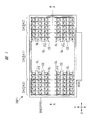
- FIG. 1 is a plan view illustrating an example of a display device according to one embodiment.
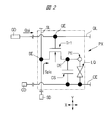
- FIG. 2 is a circuit block diagram illustrating a configuration example of a circuit included in each of a plurality of pixels illustrated in FIG. 1.
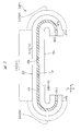
- FIG. 2 is a sectional view taken along line AA in FIG. 1.
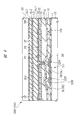
- FIG. 2 is an enlarged sectional view of a part of a display area of FIG. 1.
- FIG. 4 is an explanatory diagram illustrating an example of a relationship between an alignment axis of an alignment film and a polarization axis of ultraviolet light applied to the alignment film.
- FIG. 5 is an enlarged cross-sectional view illustrating a configuration example of an alignment film illustrated in FIG. 4.
- FIG. 5 is an enlarged cross-sectional view illustrating a configuration example of an alignment film illustrated in FIG. 4.
- FIG. 7 is an enlarged cross-sectional view of an alignment film of a display device that is a modification example of FIG.
- FIG. 9 is a perspective view of a display device that is a modification example of FIG. 1.
- FIG. 9 is a plan view when the display device shown in FIG. 8 is expanded.
- FIG. 10 is an enlarged sectional view taken along line AA of FIG. 9.
- FIG. 11 is an enlarged cross-sectional view of a display device that is a modification example of FIG. 10.
- FIG. 12 is an enlarged cross-sectional view of a display device that is a modification example of FIG. 11.
- FIG. 4 is an enlarged cross-sectional view showing, in an enlarged manner, the periphery of a boundary between alignment films separated from each other in a display device that is a modification example of FIG. 3.
- FIG. 14 is an enlarged plan view of the portion shown in FIG. 13 viewed from the display surface side.
- FIG. 14 is an enlarged cross-sectional view of a display device that is a modification example of FIG. 13.
- FIG. 15 is an enlarged plan view of a display device that is a modification example of FIG. 14.
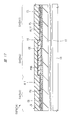
- FIG. 17 is an enlarged sectional view taken along line AA of FIG. 16.
- FIG. 3 is an enlarged plan view of a display device that is a modification example of FIG. 1.
- FIG. 19 is an enlarged sectional view taken along line AA of FIG. 18.
- FIG. 19 is an enlarged plan view of a display device that is a modification example of FIG. 18.
- FIG. 1 is a plan view illustrating an example of the display device of the present embodiment.
- the boundary between the display area DA and the peripheral area PFR in a plan view is indicated by a two-dot chain line.
- a part of a circuit block or a wiring of a circuit included in the display device DSP2 is schematically illustrated by a solid line.
- FIG. 2 is a circuit block diagram illustrating a configuration example of a circuit included in each of the plurality of pixels illustrated in FIG.
- FIG. 3 is a sectional view taken along line AA of FIG.
- FIG. 3 is a cross-sectional view, hatching is omitted except for the liquid crystal layer LQ and the sealing material BND for easy viewing.
- the display device DSP2 which is a liquid crystal display device, includes a substrate 10, a substrate 20, and a liquid crystal layer LQ shown in FIG. It has various components. In FIG. 3, these components are not shown.
- FIG. 4 is an enlarged sectional view of a part of the display area of FIG.
- the substrate SUB1 shown in FIG. 3 includes, in addition to the substrate 10 shown in FIG. 4, a plurality of insulating layers, a pattern of transistors Tr1, wiring, and the like, and an alignment film AF1.
- the substrate SUB2 shown in FIG. 3 includes a color filter CF, a light-shielding film BM, an insulating film OC1, and an alignment film AL2 in addition to the substrate 20 shown in FIG. In FIG. 3, these members included in the substrate SUB1 and the substrate SUB2 are not shown.
- the display device DSP1 of the present embodiment has a display area DA in which an image is formed in accordance with an externally supplied input signal.
- the display area DA is an effective area for displaying an image visually recognized by a viewer.
- the display area DA has an area (first area) DA1, an area (second area) DA2, and an area (third area) DA3.
- the area DA2 and the area DA3 are bendable areas.
- the area DA2 and the area DA3 have a structure that is assumed to be bent during use or while being carried.
- the area DA1 is an area that is not assumed to be bent (in other words, is not bendable).
- the above-described structure that is assumed to be bent means that, in addition to a structure that can be simply bent physically, measures against a problem caused by bending the display area DA are taken. Therefore, for example, the area DA1 may have a structure that can be physically bent. The details of the problem caused by bending the display area DA will be described later.
- the display device DSP1 has a peripheral region PFR around the display region DA in plan view.
- a sealing material BND surrounding the periphery of the display area DA.
- a plurality of wirings connected to a plurality of transistors arranged in the display area DA.
- a plurality of pixels PX are arranged in the display area DA.
- the plurality of pixels PX are arranged in a matrix along the X direction and the Y direction crossing the X direction.
- Each of the pixels PX includes a transistor Tr1 (see FIG. 2) functioning as a pixel selection switch, and a pixel electrode PE (see FIG. 2) connected to the transistor Tr1.
- the display area DA there are a plurality of scanning lines (gate lines) GL extending along the X direction and a plurality of video signal lines (source lines) SL extending along the Y direction.
- the plurality of scanning lines GL are arranged in the X direction
- the plurality of video signal lines SL are arranged in the Y direction.
- there is a common electrode CE is an electrode that supplies a common potential applied to each of the pixels PX, and for example, overlaps with a plurality of pixels PX.
- Each of the plurality of video signal lines SL is connected to the pixel electrode PE via the transistor Tr1, as shown in FIG. Specifically, the video signal line SL is connected to the source electrode SE of the transistor Tr1, and the pixel electrode PE is connected to the drain electrode DE of the transistor Tr1.
- the video signal Spic is supplied to the pixel electrode PE from the video signal line SL.
- the video signal Spic is supplied from the signal line driving circuit SD.
- the video signal line SL in the display area DA is electrically connected to the signal line drive circuit SD via a connection wiring (also referred to as a lead wiring).
- the signal line driving circuit SD supplies the video signal Spic to the pixel electrode PE included in each of the plurality of pixels PX via the video signal line SL.
- the signal line drive circuit SD is arranged outside the display area DA shown in FIG. 1 (for example, in the peripheral area PFR, or in a wiring board or a semiconductor component connected to the substrate SUB1 in the peripheral area PFR).
- Each of the plurality of scanning lines GL drives the transistor Tr1, as shown in FIG. Specifically, a part of the scanning line GL forms a gate electrode GE of the transistor Tr1.
- Each of the plurality of scanning lines GL is drawn out to a peripheral region PFR outside the display region DA, and is connected to a scanning line driving circuit (gate driving circuit) GD shown in FIG.
- the scanning line driving circuit GD is a scanning signal output circuit that outputs a scanning signal Gsi input to the plurality of scanning lines GL.
- the scanning line driving circuit GD is arranged in the peripheral region PFR shown in FIG.
- the transistor Tr1 is a thin film transistor (TFT) that functions as a selection switch for selecting the pixel PX.
- the scanning line GL includes the gate electrode GE of the transistor Tr1.
- the display device DSP1 includes the substrate 10. Further, the display device DSP1 includes a substrate 20 facing the substrate 10 via the liquid crystal layer LQ.
- the substrate 10 has a front surface (main surface, front surface) 10f facing the liquid crystal layer LQ, and a back surface (main surface, back surface) 10b opposite to the front surface 10f.
- the substrate 20 has a back surface (main surface, back surface) 20b facing the liquid crystal layer LQ and a front surface (main surface, front surface) 20f opposite to the back surface 20b.
- the substrate 10 has a region (first region) DA1, a region (second region) DA2, and a region (third region) DA3 on each of the front surface 10f and the back surface 10b.
- the substrate 20 has a region (first region) DA1, a region (second region) DA2, and a region (third region) DA3 on each of the front surface 20f and the rear surface 20b.
- each of the substrate 10 and the substrate 20 can be bent in the region DA2 and the region DA3. Therefore, each of the substrate 10 and the substrate 20 has flexibility at least in the region DA2 and the region DA3. In the case of the present embodiment, the substrate 10 and the substrate 20 have flexibility in the region DA1, the region DA2, and the region DA3. In order to impart flexibility to the substrate 10 and the substrate 20, the substrate 10 and the substrate 20 are made of, for example, a resin material (organic material) containing a polymer such as polyimide, polyamide, polycarbonate, or polyester.
- the circuit component including the transistor Tr1 included in the pixel PX shown in FIG. 2 is formed on the substrate 10 as shown in FIG.
- the display device DSP1 has an insulating film 11 on the front surface 10f of the substrate 10 in the display area DA.
- the insulating film 11 is a base layer of various circuits including a TFT, and is made of, for example, an inorganic insulating material such as silicon nitride (SiN) or silicon oxide (SiO).
- FIG. 4 exemplarily shows one transistor Tr1.
- the transistor Tr1 is a thin film transistor (TFT).
- the transistor Tr1 includes a semiconductor region (semiconductor layer) SCR that forms a channel region, a source region, and a drain region.
- the semiconductor region SCR is made of, for example, polysilicon and is formed on the insulating film 11.
- a conductor pattern CDP connected to the source electrode SE or the drain electrode DE of the transistor Tr1 is formed in the source region and the drain region.
- the conductor pattern CDP is formed by, for example, a sputtering method.
- the semiconductor region SCR is covered with the insulating film 12 which is a gate insulating film.
- the insulating film 12 is made of, for example, silicon oxide, and is deposited on the semiconductor region SCR and the conductor pattern CDP by, for example, chemical vapor deposition (CVD).
- a gate electrode GE is formed on the insulating film 12.
- the gate electrode GE is formed at a position overlapping the channel region of the semiconductor region SCR. In other words, the channel region of the semiconductor region SCR faces each other via the insulating film 12 that is a gate insulating film.
- the gate electrode GE is formed by patterning a metal film formed by a sputtering method or the like.
- a plurality of scanning lines GL shown in FIG. 1 are formed in the same layer as the gate electrode GE.
- the gate electrode GE and the insulating film 12 are covered with the insulating film 13.
- the insulating film 13 is made of, for example, silicon nitride, silicon oxide, or a laminated film thereof.
- the insulating film 13 is formed by, for example, a CVD method.
- a contact hole penetrating the insulating films 12 and 13 in the thickness direction is formed in the insulating films 12 and 13, and the source electrode SE is connected to the conductor pattern CDP on the source region via the contact hole.
- the drain electrode DE is connected to the conductor pattern CDP on the drain region via a contact hole.
- the source electrode SE and the drain electrode DE are formed by, for example, a sputtering method.
- a plurality of video signal lines SL shown in FIG. 1 are formed in the same layer as the source electrode SE and the drain electrode.
- the source electrode SE, the drain electrode DE, and the insulating film 13 are covered with the insulating film 14.
- the insulating film 14 is made of, for example, silicon nitride, silicon oxide, or a stacked film thereof.
- the insulating film 14 is formed by, for example, a CVD method.
- an organic film (planarizing film, organic insulating film) 15 is formed on the insulating film 14.
- the organic film 15 is made of an organic material such as an acrylic resin.
- the thickness of the organic film 15 is larger than the thickness of each of the other insulating films 11, 12, 13, and 14. Further, the organic film 15 covers the transistor Tr1.
- the common electrode CE is formed on the organic film 15.
- a common drive potential corresponding to the plurality of pixels PX (see FIG. 1) is supplied to the common electrode CE.
- the common drive potential is supplied from the common electrode drive circuit CD shown in FIG.
- the common electrode CE is arranged over the entire display area DA.
- the common electrode CE is made of a transparent conductive material such as ITO (Indium Tin Oxide) or IZO (Indium Zinc Oxide).
- the common electrode CE is covered with the insulating film 16.
- the insulating film 16 is made of, for example, silicon nitride, silicon oxide, or a stacked film thereof.
- the insulating film 16 is formed by, for example, a CVD method.
- the pixel electrode PE is formed on the insulating film 16.
- the common electrode CE and the pixel electrode PE are formed in different layers.
- a plurality of common electrodes CE and a plurality of pixel electrodes PE may be formed on the same surface (for example, on the organic film 15), and may be alternately arranged so as to be adjacent to each other.
- the pixel electrode PE is preferably made of, for example, a transparent conductive material such as ITO or IZO or a metal material.
- the pixel electrode PE is connected to the drain electrode DE via a contact hole formed to penetrate the insulating film 16 and the organic film 15.
- the alignment film AL1 is an insulating film having a function of aligning the initial alignment of the liquid crystal molecules included in the liquid crystal layer LQ, and is made of, for example, a polyimide resin.
- the alignment film AL1 is between the substrate 10 and the liquid crystal layer LQ and is in contact with the liquid crystal layer.
- the alignment film AL1 is in contact with the liquid crystal layer LQ. Details of the alignment film AL1 will be described later.
- the display device DSP1 has a light-shielding film BM, a color filter CF, an insulating film OC1, and an alignment film AL2 between the back surface (main surface, surface) 20b of the substrate 20 and the liquid crystal layer LQ.
- the color filter CF is formed on the back surface 20 b side of the substrate 20.
- three color filters CF of red (R), green (G), and blue (B) are periodically arranged.
- a light-shielding film BM is arranged at a boundary between the color filters CF of the respective colors.
- the light shielding film BM is called a black matrix, and is made of, for example, a black resin or a low-reflection metal.
- the light-shielding film BM is formed, for example, in a lattice shape in plan view.
- the insulating film OC1 shown in FIG. 4 covers the color filter CF.
- the insulating film OC1 functions as a protective film for preventing impurities from diffusing from the color filter into the liquid crystal layer.
- the insulating film OC1 is an organic insulating film made of, for example, an acrylic photosensitive resin.
- the alignment film AL2 is disposed on the insulating film OC1.
- the alignment film AL2 is between the substrate 20 and the liquid crystal layer LQ and is in contact with the liquid crystal layer LQ.
- Each of the alignment films AL1 and AL2 is a photo-alignment film that is subjected to an alignment process by irradiating polarized ultraviolet light.
- FIG. 5 is an explanatory diagram illustrating an example of the relationship between the alignment axis of the alignment film and the polarization axis of the ultraviolet light applied to the alignment film.
- the alignment films AL1 and AL2 are films obtained by imidizing polyamic acid or polyamic acid ester.
- the optical alignment treatment on the alignment films AL1 and AL2 is performed by irradiating the alignment films AL1 and AL2 with polarized ultraviolet light having a wavelength of, for example, about 250 nm.
- the alignment film AL1 and the alignment film AL2 the alignment film AL1 formed between the substrate 10 and the liquid crystal layer LQ shown in FIG. The same is true for the alignment film AL2 formed between them.
- the technology described for the alignment film AL1 can be applied to the alignment film AL2.
- the alignment film AL1 has an X-direction alignment axis ALP crossing the Y direction by irradiating the alignment film AL1 with ultraviolet light having the Y-direction polarization axis UVP.
- the alignment film AL1 includes a polyimide PI1 whose main chain direction is randomly arranged in various directions on the XY plane.
- the polyimide PI1 when the alignment film AL1 is irradiated with ultraviolet light having a polarization axis UVP, the polyimide PI1 whose main chain direction is arranged parallel to the polarization axis UVP of the ultraviolet light absorbs a large amount of polarized ultraviolet light, As schematically shown in FIG.
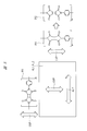
- the cyclobutane ring contained in the polyimide PI1 is cleaved, resulting in a composition PI2 in which the polyimide PI1 is divided.
- the polyimide PI1 arranged so that the main chain direction is orthogonal to the polarization axis UVP of the ultraviolet ray hardly absorbs the ultraviolet ray and is not divided.
- composition PI2 from which the polyimide PI1 is divided does not contribute to the alignment of liquid crystal molecules, and the undivided polyimide PI1 contributes to the alignment of liquid crystal molecules. For this reason, by irradiating an ultraviolet ray having a polarization axis UVP, the polyimide PI1 having a main chain in a direction parallel to the polarization axis UVP is selectively divided, so that a direction orthogonal to the polarization axis UVP is obtained. An alignment film AL1 having an alignment axis ALP is obtained.
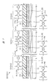
- FIG. 6 is an enlarged sectional view showing a configuration example of the alignment film shown in FIG.
- the boundaries between the films are clearly shown in order to clearly show that the alignment film AL1 has a structure in which films having different component ratios are stacked.
- the boundaries between the films may not always be clear. is there. Further, a film in which both film materials are mixed may exist between the two films.
- the alignment film AL1 of the present embodiment has a film (part) L1A in the region DA1 and a film (part) L1B between the film L1A and the substrate 10. Further, the alignment film AL1 has a film (part) L2A in the region DA2 and a film (part) L2B between the film L2A and the substrate 10.
- the thickness of the film L2A of the alignment film AL1 included in the display device DSP1 is smaller than the thickness of the film L1A. Further, the thickness of the film L2B of the alignment film AL1 is larger than the thickness of the film L1B.
- the thickness of the alignment film AL1 is substantially the same in the region DA1 and the region DA2.
- the thicknesses of the film L1A and the film L1B arranged in the region DA1 are substantially the same (half the thickness of the alignment film AL1).
- the thickness of the film L2A disposed in the region DA2 is smaller than the thickness of the film L2B.
- the thickness of the film L2A is about 25% of the thickness of the film L2B.
- each of the film L1A and the film L2A of the alignment film AL1 contains a photodecomposable material as a main component like the polyimide PI1 shown in FIG.
- the film L2A and the film L2B are made of different materials.
- the film L1A and the film L1B are made of different materials. In the example shown in FIG.
- the material of the film L1A and the film L2A of the alignment film AL1 is a polyimide PIA1 having a 1,3-dimethylcyclobutane skeleton
- the material of the film L1B and the film L2B is a polyimide having a pyromellitic imide skeleton.
- a polyimide PIA1 having a cyclobutane skeleton having a substituent represented by a 1,3-dimethylcyclobutane skeleton is compared with a polyimide having an unsubstituted cyclobutane skeleton like polyimide PI1 shown in FIG.
- the cyclobutane ring is easily cleaved.
- the polyimide PIA1 has a higher decomposition sensitivity to ultraviolet light than the polyimide PI1, so that the alignment characteristics can be easily controlled by the photo-alignment treatment.
- the polyimide PIB shown in FIG. 6 has higher mechanical strength than the polyimide PIA1.
- the films L1B and L2B having high mechanical strength are disposed as the underlayers of the films L1A and L2A having high orientation characteristics and having low mechanical strength. Even when the L2A layer is bent, it is reinforced by the underlying layer.
- a 1,3-dimethylcyclobutane skeleton an example of a cyclobutane skeleton having a substituent.
- the thickness of the film L2A mainly including polyimide PIA1 having low mechanical strength is smaller than the thickness of the film L1A.
- the thickness of the film L2B for reinforcing the strength of the film L2A is larger than the thickness of the film L1B in the region DA1.
- the mechanical strength of the alignment film AL1 including the film L2A and the film L2B is sufficient in the region DA2. Therefore, even when the alignment film AL1 is bent in the region DA2, it is possible to prevent a part of the alignment film AL1 from peeling off.
- the area DA3 is also a bendable area. Therefore, the area DA3 has the same structure as the area DA2. That is, the alignment film AL1 has a film L3A overlapping the region DA3, and a film L3B between the film L3A and the substrate 10.
- the thickness of the film L3A of the alignment film AL1 included in the display device DSP1 is smaller than the thickness of the film L1A. Further, the thickness of the film L3B of the alignment film AL1 is larger than the thickness of the film L1B.
- the thickness of the alignment film AL1 is substantially the same in the region DA1 and the region DA3.
- the thickness of the film L3A disposed in the area DA2 is smaller than the thickness of the film L3B.
- the thickness of the film L3A is about 25% of the thickness of the film L3B. For this reason, even when the area DA3 is bent, it is possible to suppress the display quality of the area DA3 from being deteriorated due to the debris from which the alignment film AL1 has peeled off.
- each material of the film L1B, the film L2B, and the film L3B is a polyimide PIB having a pyromellitic imide skeleton.
- polyimide PIB having a pyromellidimide skeleton since it does not have a cyclobutane ring in the main chain, it is hard to be divided even when irradiated with ultraviolet rays when performing the photo-alignment treatment.
- the polyimide PIB shown in FIG. 6 has higher mechanical strength than the polyimide PIA1. As shown in FIG.
- the films L1B, L2B, and L3B having high mechanical strength are arranged as the underlayers of the films L1A, L2A, and L3A having the high alignment characteristics, so that the film L2A is formed. Even when the film L3A is bent, it is reinforced by the underlayer.
- each of the film L1B, the film L2B, and the film L3B contains a polyimide PIA1 containing a cyclobutane ring.
- a polyimide acid having a cyclobutane ring (in other words, a polyamide material having a cyclobutane ring) is imidized like polyimide PIA1 shown in FIG. It is a polyimide obtained. Therefore, in the film L1A shown in FIG. 6, the mass ratio of the polyimide obtained by imidizing a polyamic acid or a polyamic acid ester containing a cyclobutane ring is preferably 80% or more.
- a structural example of a polyamic acid or polyamic acid ester containing a cyclobutane ring is represented by the following chemical formula (1).
- R 1 is each independently an alkyl group having 1 to 8 carbon atoms and a hydroxyl group (OH).
- Ar is an aromatic compound.
- the polyimide contained in each of the films L1B, L2B, and L3B shown in FIG. 6 is preferably a polyimide obtained by imidizing a polyamic acid containing no cyclobutane ring.
- the film L1B, the film L2B, and the film L3B illustrated in FIG. 6 may each include a polyimide obtained by imidizing a polyamic acid ester containing a cyclobutane ring.
- An example of the structure of a polyamic acid containing no cyclobutane ring is represented by the following chemical formula (2).
- R1 is each independently an alkyl group having 1 to 8 carbon atoms and a hydroxyl group (OH).
- Ar is an aromatic compound.
- the film L1A and the film L1B shown in FIG. 6 have different materials as main components, the components constituting the film L1A by using a highly polar diamine for the Ar portion exemplified in the chemical formula (2). And the components constituting the film L2B can be separated in a self-aligned manner. That is, by using a highly polar diamine for the Ar portion exemplified in the chemical formula (2), the surface energy of the polyamic acid is increased, so that the pixel electrode PE (see FIG. 4) which is a base film of the alignment film AL1 and The affinity for the organic film 15 (see FIG. 4) is increased.
- the polyamic acid containing no cyclobutane ring is attracted near the base film, and the polyamic acid represented by the chemical formula (2) is distributed more in the film L1B than in the film L1A.
- the film L1B contains a large amount of polyimide having no cyclobutane ring in the main chain, such as polyimide PIB shown in FIG.
- a polyimide containing a cyclobutane ring in the main chain such as the polyimide PIA1 shown in FIG. 6, is widely distributed in the film L1A.
- the material of the film L1A of the alignment film AL1 is the same as the material of the film L2A.
- the material of the film L1A of the alignment film AL1 and the material of the film L2A may be different from each other.
- a polyimide PIA2 having an unsubstituted cyclobutane skeleton is used as a main component.
- FIG. 7 is an enlarged sectional view of an alignment film of a display device which is a modification example of FIG.
- the mechanical strength of the film L2A can be increased as compared with the display device DSP1, so that the peeling of the alignment film AL2 can be further suppressed.
- the material of the film L1A of the alignment film AL1 is the same as the material of the film L1B, as in the display device DSP1.
- the material of the film L1A of the alignment film AL1 is different from the material of the film L2A.
- the material of the film L1A of the alignment film AL1 is polyimide PIA1 having a 1,3-dimethylcyclobutane skeleton.
- the material of the film L2A of the alignment film AL1 is polyimide PIA2 having an unsubstituted cyclobutane skeleton.
- the polyimide PIA1 having a 1,3-dimethylcyclobutane skeleton is more prone to cleavage of the cyclobutane ring when irradiated with ultraviolet light than the polyimide PIA2 having an unsubstituted cyclobutane skeleton.
- the polyimide PIA1 has a higher decomposition sensitivity to ultraviolet light than the polyimide PIA2, so that the alignment characteristics can be easily controlled by the photo-alignment treatment.
- the polyimide PIA2 has a lower decomposition sensitivity to ultraviolet light than the polyimide PIA1, so that the film L2A of the alignment film AL1 has higher mechanical strength when bent than the film L1A.
- the film L2A made of the polyimide PIA2 is arranged in the area DA2 where bending is assumed, and the film L1A made of the polyimide PIA1 is arranged in the area DA1 where bending is not assumed.
- the film L1A of the alignment film AL1 disposed in the region DA1 has better alignment characteristics than the film L2A of the alignment film AL1 disposed in the region DA2, display quality can be improved.
- the film L2A having high mechanical strength against bending is arranged in the region DA2, peeling of the alignment film AL1 due to bending can be suppressed. As a result, it is possible to suppress the display quality of the area DA2 from being degraded due to the debris from which the alignment film AL1 has peeled off.
- a step of applying a polyimide raw material liquid to each region in order to make the polyimide contained in the film L1A and the polyimide contained in the film L2A become different types of polyimide, a step of applying a polyimide raw material liquid to each region. In this case, it is preferable to apply a different material to each region. Also, as shown in FIG. 6, even when the thickness of the film L1A and the thickness of the film L2A are made different, it is preferable to apply a polyimide raw material having a different blending ratio for each region in the raw material liquid application stage. .
- a polyimide PIA1 having a 1,3-dimethylcyclobutane skeleton is formed in the region DA1 by imidization treatment (for example, heat treatment at about 230 ° C. or dehydration / reduction treatment using a catalyst).
- imidization treatment for example, heat treatment at about 230 ° C. or dehydration / reduction treatment using a catalyst.
- a coating material containing a polyamic acid to become a polyimide PIB having a pyromellitic imide skeleton is applied.
- the region DA2 and the region DA3 are coated with a polyamic acid that becomes a polyimide PIA2 having an unsubstituted cyclobutane skeleton by imidization treatment and a polyamic acid that becomes a polyimide PIB having a pyromellidimide skeleton by imidization treatment.
- Material is applied. As described above, when applying different coating materials to each region, it is preferable to apply the materials by an inkjet method. Another method for separating the film L1A and the film L2A of the alignment film AL1 will be described later.
- FIG. 8 is a perspective view of a display device which is a modification example of FIG.
- FIG. 9 is a plan view when the display device shown in FIG. 8 is expanded.
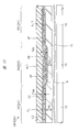
- FIG. 10 is an enlarged sectional view taken along line AA of FIG.
- the size of the display device DSP3 can be reduced by folding the display area DA.
- the display device DSP3 can visually recognize an image on a large screen by expanding the folded display area DA as illustrated in FIG.
- the display area DA is connected to the plurality of pixels PX including the transistor Tr1 (see FIG. 2) and the plurality of pixels PX, similarly to the display device DSP2 illustrated in FIG.
- the scanning lines GL, the video signal lines SL, the common electrodes CE, and the like are arranged.
- the region DA2 since the region DA2 is bent, it is necessary to suppress the peeling of the alignment film AL1 (see FIG. 10) when the region DA2 is bent, as in the case of the display device DSP1 shown in FIG.
- the method described with reference to FIGS. 7 and 6 may be applied, but in this embodiment, another method will be described.
- the display device DSP3 has the organic film 15 between the substrate 10 and the alignment film AL1.
- the organic film 15 is a planarization film that covers the transistor Tr1, as shown in FIG.
- the thickness TH1 of the organic film 15 at a position overlapping the region DA2 is smaller than the thickness TH2 of the organic film 15 at a position overlapping the region DA1.
- the coating liquid that becomes the alignment film AL1 is a liquid material having low viscosity at the stage of coating. Therefore, when the surface to be coated has irregularities, the coating liquid is applied to the concave portions thicker than the convex portions.
- the thickness TH3 of the alignment film AL1 at the position overlapping the region DA2 is larger than the thickness TH4 of the alignment film AL1 at the position overlapping the region DA1.
- the entire alignment film AL1 may be a polyimide having a cyclobutane skeleton, such as the polyimide PIA1 and the polyimide PIA2 shown in FIG.
- the alignment film AL1 of the display device DSP3 is made of a polyamide containing no cyclobutane ring, like the display device DSP1 described with reference to FIG. It is preferable to include a polyimide obtained by imidizing an acid (for example, a polyimide PIB having a pyromellitic imide skeleton shown in FIGS. 6 and 7).
- the alignment film AL1 of the display device DSP3 shown in FIG. 10 has a multi-layer structure at a position overlapping with each of the region DA1 and the region DA2. Comparing the thicknesses of the film L1A (see FIG. 6) and the film L2A (see FIG. 6) in contact with the layer LQ, it is preferable that the thickness of the film L2A of the alignment film AL1 is smaller than the thickness of the film L1A. Thereby, even when the area DA2 is bent, the alignment film AL1 is more difficult to peel off.
- the alignment film AL1 of the display device DSP3 shown in FIG. 10 is made of a polyimide having a dimethylcyclobutane ring such as a polyimide PIA1 having a 1,3-dimethylcyclobutane skeleton in the region DA1. Is preferably arranged, and the polyimide PIA2 having an unsubstituted cyclobutane ring is preferably arranged in the region DA2.
- the application amount per unit area in the region DA2 is changed in the step of applying the coating liquid as the raw material of the alignment film AL1 in the region DA1. Make it larger than the application amount per unit area.
- an alignment film AL1 having a structure in which the thickness TH3 is greater than the thickness TH4 and having different materials in the region DA1 and the region DA2 is obtained.
- the display device DSP3 is the same as the display device DSP1 described with reference to FIGS. 1 to 6 or the display device DSP2 illustrated in FIG. Therefore, duplicate description will be omitted.
- the technology described with reference to FIGS. 8 to 10 for example, the technology for improving the mechanical strength of the bendable area DA2 by reducing the thickness of the organic film 15 is used.
- FIG. 11 is an enlarged sectional view of a display device which is a modification example of FIG.
- the display device DSP4 shown in FIG. 11 has the organic film 15 between the substrate 10 and the alignment film AL1.
- the organic film 15 is a planarization film that covers the transistor Tr1, as shown in FIG.
- the display device DSP4 has an insulating film 16 which is an inorganic film covering the organic film 15.
- the insulating film 16 is an inorganic insulating film provided between the plurality of pixel electrodes PE and the common electrode CE shown in FIG.
- the insulating film 16 has an opening 16H at a position overlapping the region DA2.
- the alignment film AL1 is in contact with the organic film 15 via the opening 16H of the insulating film 16.
- the organic film 15 has higher hydrophobicity than the insulating film 16 which is an inorganic film.
- the distribution of the type of polyimide in the alignment film AL1 can be controlled. For example, when the polyamic acid or polyamic acid ester containing a cyclobutane ring shown in the chemical formula (1) described above is compared with the polyamic acid containing no cyclobutane ring shown in the chemical formula (2), the polyamic acid shown in the chemical formula (2) is compared. Has a higher affinity with the organic film 15.
- the position of the chemical formula (2) becomes closer to the organic film 15.
- the indicated polyamic acid containing no cyclobutane ring is likely to aggregate.
- the polyamic acid containing a cyclobutane ring represented by the chemical formula (1) tends to gather at a position away from the organic film 15, that is, at the front surface AL1f side of the alignment film AL1.
- the organic film 15 and the alignment film AL1 are in contact with each other at a position overlapping the region DA2.
- the alignment film AL1 is more likely to be gathered in the lower film (the film farther from the liquid crystal layer LQ) as the material has a higher affinity for the organic film 15. Therefore, for example, when the alignment film AL1 includes the film L2A and the film L2B as shown in FIG. 6, the film L2B contains more polyimide PIB having a high affinity for the organic film 15, and the film L2A contains the polyimide PIB.
- the amount of polyimide PIA2 having low affinity for is increased.
- FIG. 11 since the pixel PX (see FIG. 1) also exists in the area DA2, the common electrode CE is arranged in the area DA2. However, for example, when the area DA2 is narrow and the pixel PX is not arranged in the area DA2, the common electrode CE may not be arranged.
- the insulating film 16 and the common electrode CE illustrated in FIG. 11 do not exist at a position overlapping the region DA2.
- FIG. 12 is an enlarged sectional view of a display device which is a modification example of FIG. In the case of the display device DSP5, the organic film 15 and the alignment film AL1 are in contact with each other at the entire position overlapping the region DA2.
- the display devices DSP4 and DSP5 are the same as the display device DSP1 described with reference to FIGS. 1 to 6, the display device DSP2 shown in FIG. 7, or the display device DSP3 shown in FIGS. The same is true. Therefore, duplicate description will be omitted.
- the technology described in this embodiment may be applied in combination with the technology described in another embodiment.
- the display device DSP4 is applied to a display device in which the display area DA is folded, similarly to the display device DSP3 illustrated in FIG.
- the present invention may be applied to a display device of a type in which the region adjacent to the region DA1 is bent, like the display device DSP1 shown in FIG.
- FIG. 13 is an enlarged cross-sectional view showing, in an enlarged manner, the vicinity of a boundary between alignment films separated from each other in a display device that is a modification example of FIG.
- FIG. 14 is an enlarged plan view of the portion shown in FIG. 13 viewed from the display surface side.
- FIG. 14 is a plan view, but shows the member SW1 with hatching. Note that the overall structure of the display device DSP6 shown in FIGS. 13 and 14 is the same as the structure of the display device DSP1 shown in FIGS. 1 and 3 or the structure of the display device DSP3 shown in FIGS.
- the display device DSP6 has flexibility, a substrate 10 having a region DA1 and a region DA2 on a front surface (main surface, front surface) 10f, a liquid crystal layer LQ, and an alignment film which is in contact with the liquid crystal layer LQ and has photodegradability.
- AL1 The substrate 10 can be bent in the area DA2.
- the alignment film AL1 includes an alignment film AL11 overlapping the region DA1 and an alignment film AL12 overlapping the region DA2.
- a member SW1 that separates the alignment films AL11 and AL12 from each other is disposed between the alignment films AL11 and AL12 in plan view.
- the member SW1 is a structure made of, for example, an organic material such as a resin, and extends in the Y direction along a boundary between the region DA1 and the region DA2.
- the top (front) SWf of the member SW1 is located at a position higher than the front AL1f of the alignment film AL1 (on the side of the substrate 20 shown in FIG. 3).
- the distance from the substrate 10 to the top SWf of the member SW1 is longer than the distance from the substrate 10 to the front surface AL1f of the alignment film AL1.
- the member SW1 protrudes from the front surface AL1f of the alignment film AL1. Therefore, the member SW1 functions as a separation wall that separates the alignment films AL11 and AL12.
- the materials of the alignment film AL11 and the alignment film AL12 are formed of different materials. Easy to do.
- the member SW1 is formed before applying the material of the alignment film AL1.
- the material of the alignment film AL11 is applied to a position overlapping the region DA1
- the material of the alignment film AL12 is applied to a position overlapping the region DA2.
- the material is heated to about 230 ° C. to perform an imidization process on the raw material of the polyimide.
- a photo-alignment treatment is performed by irradiating the imidized alignment film AL1 with ultraviolet rays.
- the display device DSP6 since the alignment films AL11 and AL12 can be reliably separated from each other, when the constituent materials of the alignment films AL11 and AL12 are different from each other, the boundary between the alignment films AL11 and AL12 is formed. Of the materials can be suppressed.
- the display device DSP1 shown in FIG. 6 or the display device DSP2 shown in FIG. 7 it is necessary to apply different coating materials to the region DA1 and the region DA2. In this case, it is effective to arrange the member SW1 at the boundary between the area DA1 and the area DA2 as in the display device DSP6.
- each of the alignment film AL11, the alignment film AL12, and the member SW1 is formed on the same base film.
- each of the alignment film AL11, the alignment film AL12, and the member SW1 is formed on the insulating film 16 which is an inorganic insulating film.
- the alignment film AL11 and the alignment film AL12 can be reliably separated.
- FIG. 15 is an enlarged sectional view of a display device which is a modification example of FIG.
- the member SW2 shown in FIG. 15 extends in the Y direction along the boundary between the region DA1 and the region DA2, similarly to the member SW1 shown in FIG.
- the member SW2 shown in FIG. 15 has liquid repellency to the varnish material contained in the alignment film AL1.
- the liquid-repellent phenomenon occurs, for example, according to the following principle.
- the raw material of the alignment film AL11 and the raw material of the alignment film AL12 are varnish materials each containing a solvent.
- the member SW2 is formed, for example, by applying a raw material application liquid to a boundary between the region DA1 and the region DA2, and then curing the material by heating.
- the cured member SW2 has poor compatibility (hard to melt) with the solvent containing the varnish material. In this case, at the contact interface between the member SW1 and the alignment film AL1, they are repelled and separated from each other (in other words, liquid-repellent).
- the alignment film AL11 and the alignment film AL12 are separated from each other by utilizing the above-described liquid repellency phenomenon.
- the height of the top SWf is set to be substantially the same as the height of the front surface AL1f of the alignment film AL1. can do. If the height of the top portion SWf can be reduced like the member SW2, it is possible to prevent the alignment film AL1 and the alignment film AL2 (see FIG. 4) from being damaged by contact with the top portion of the member SW2.
- the display devices DSP6 and DSP7 are the same as the display device DSP1 described with reference to FIGS. 1 to 6, the display device DSP2 shown in FIG. 7, or the display device DSP3 shown in FIGS. The same is true. Therefore, duplicate description will be omitted. Note that the technology described in this embodiment may be applied in combination with the technology described in another embodiment.
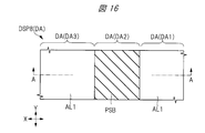
- FIG. 16 is an enlarged plan view of a display device which is a modification example of FIG.
- FIG. 17 is an enlarged sectional view taken along line AA of FIG.
- the overall structure of the display device DSP8 shown in FIGS. 16 and 17 is the same as the structure of the display device DSP3 shown in FIGS. 8 and 9, for example.
- the display device DSP8 has flexibility, is in contact with the substrate 10 having the region DA1, the region DA2, and the region DA3 on the front surface (main surface, front surface) 10f, the liquid crystal layer LQ, and the liquid crystal layer LQ. And an alignment film AL1.
- the substrate 10 can be bent in the area DA2.
- the area DA2 is between the area DA1 and the area DA3.
- the areas DA1 and DA3 are areas that are not assumed to be bent.
- a member PSB projecting from the insulating film 16 which is a base film of the alignment film AL1 toward the liquid crystal layer LQ is arranged in the area DA2. As shown in FIG. 16, the member PSB extends in the Y direction along the extending direction of the area DA2.
- the thickness of the alignment film AL1 on the member PSB is equal to the alignment film AL1 at the position overlapping the regions DA1 and DA3. Thinner than the thickness of. Further, depending on the height of the member PSB, the alignment film AL1 may not be disposed on the member PSB. As described above, when there is almost no alignment film AL1 in the region DA2 which is a bendable region, it is not necessary to consider that the alignment film AL1 is cut off even if the region DA2 is bent.
- the display device DSP8 is similar to the display device DSP1 described with reference to FIGS. 1 to 6, the display device DSP2 shown in FIG. 7, or the display device DSP3 shown in FIGS. Therefore, duplicate description will be omitted. Note that the technology described in this embodiment may be applied in combination with the technology described in another embodiment.
- FIG. 18 is an enlarged plan view of a display device that is a modification example of FIG.
- FIG. 19 is an enlarged sectional view taken along line AA of FIG.
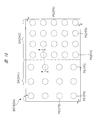
- FIG. 20 is an enlarged plan view of a display device which is a modification example of FIG. 18 and 20, the outline of the top of the spacer member PS2 having a truncated cone shape is indicated by a dotted line.
- the overall structure of the display device DSP9 is, for example, the same as the structure of the display device DSP1 shown in FIGS. 1 and 3 or the structure of the display device DSP3 shown in FIGS.
- the display device DSP9 has a substrate 20 (see FIG. 19) that faces the substrate 10 and is separated from the substrate 10 in the region DA1 and the region DA2. Further, the display device DSP9 has a plurality of spacer members PS arranged between the substrate 10 and the two substrates 20 at each of the position overlapping the area DA1 and the position overlapping the area DA2.
- each of the plurality of spacer members PS is fixed to the substrate 20 side.
- the spacer member PS only needs to be fixed to one of the substrate 10 and the substrate 20, and there are various modified examples other than FIG.
- each of the plurality of spacer members PS may be fixed to the substrate 10 side.
- a plurality of spacer members PS fixed to the substrate 10 and a plurality of spacer members PS fixed to the substrate 20 may be mixed.
- the plurality of spacer members PS include a plurality of spacer members PS1 arranged at a position overlapping the area DA1 and a plurality of spacer members PS2 arranged at a position overlapping the area DA2.
- the spacer member PS is a member that suppresses the thickness of the liquid crystal layer LQ as described above, in other words, the separation distance between the substrate 10 and the substrate 20 from becoming extremely small. Therefore, when an external force is applied to the display device DSP9 and the thickness of the liquid crystal layer LQ is temporarily reduced, the top of the spacer member PS contacts the alignment film AL1. At this time, it is preferable to prevent a part of the alignment film AL1 from peeling off due to the contact with the spacer member PS. In particular, in the area DA2 that is supposed to be bent and used, there is a high possibility that the spacer member PS2 and the alignment film AL2 come into contact with each other.
- the stress generated when each spacer member PS2 comes into contact with the alignment film AL1 is reduced by arranging the spacer members PS2 at high density in the area DA2.
- the arrangement density of the plurality of spacer members PS2 at the position overlapping the area DA2 is higher than the arrangement density of the spacer members PS1 at the position overlapping the area DA1.
- the distance between the adjacent spacer members PS2 is shorter than the distance between the adjacent spacer members PS1.
- the width PSW2 of the top of the spacer member PS2 at the position overlapping the area DA2 is wider than the width PSW1 of the top of the spacer member PS1 at the position overlapping the area DA1. It is different from the display device DSP9 shown. In other words, the area of the top of the spacer member PS2 provided in the display device DSP6 is larger than the area of the top of the spacer member PS1.
- Each of the plurality of spacer members PS has a shape such as a truncated cone or a truncated pyramid.
- the shape of the spacer member PS is a truncated cone.
- the display device DSP9 is the same as any one of the display devices DSP1 to DSP8 described above. Therefore, duplicate description will be omitted. Note that the technology described in this embodiment may be applied in combination with the technology described in another embodiment.
- each of the areas DA2 and DA3 on both sides of the area DA1 is bent so as to be curved, and as shown in FIG.
- An example of a display device that can be folded along has been described.
- a first substrate having flexibility and having a first region, a second region, and a third region on a surface;
- the display device wherein a spacer member protruding from a base film of the alignment film toward the first liquid crystal layer is arranged in the second region.
- the present invention is applicable to a display device and an electronic device in which the display device is incorporated.
Landscapes
- Physics & Mathematics (AREA)
- Nonlinear Science (AREA)
- General Physics & Mathematics (AREA)
- Crystallography & Structural Chemistry (AREA)
- Optics & Photonics (AREA)
- Chemical & Material Sciences (AREA)
- Liquid Crystal (AREA)
- Mathematical Physics (AREA)
- Engineering & Computer Science (AREA)
- Theoretical Computer Science (AREA)
- Spectroscopy & Molecular Physics (AREA)
- Microelectronics & Electronic Packaging (AREA)
- Devices For Indicating Variable Information By Combining Individual Elements (AREA)
Abstract
表示装置は、可撓性を有し、表面に領域(DA1)および領域(DA2)を有する基板(10)と、液晶層(LQ)と、液晶層(LQ)に接し、配向膜と、を備える。基板(10)は、領域DA2で折り曲げ可能であり、配向膜(AL1)は、液晶層(LQ)に接し、光分解性がある材料を含む膜(L1A)、膜(L2A)と、膜(L1A)、(L2A)と基板(10)との間にある膜(L1B)、(L2B)と、を有する。配向膜(AL1)は、領域(DA2)と重なる領域にある膜(L2A)の厚さは、領域(DA1)と重なる位置にある膜(L1A)の厚さより薄い。
Description
本発明は、表示装置に関し、例えば、折り曲げが可能な液晶表示装置に適用して有効な技術に関する。
表示装置の態様として、折り曲げ可能な表示装置が検討されている(特開2017-126061公報(特許文献1)参照)。
本願発明者は、折り曲げることが可能な表示装置の技術開発を行っている。折り曲げ可能な表示装置のうち、液晶表示装置の場合、以下の課題があることが判った。液晶表示装置の場合、光の透過を制御する液晶を配向する目的で、液晶層に接する配向膜を備える。折り曲げ可能な領域に配向膜がある場合、折り曲げた時に生じる力に起因して、配向膜の一部が部分的に剥離する場合がある。剥離した配向膜の一部が液晶層中にあると、この剥離した部分により液晶の配向が乱され、表示品質が低下する原因になる。
本発明の目的は、表示装置の性能を向上させる技術を提供することにある。
本発明の一態様である表示装置は、可撓性を有し、表面に第1領域および第2領域を有する第1基板と、液晶層と、前記液晶層に接し、光分解性がある配向膜と、を備える。前記第1基板は、前記第2領域で折り曲げ可能であり、前記配向膜は、前記液晶層に接し、光分解性を備える材料を含む第1膜を含む。前記第2領域にある前記第1膜の厚さは、前記第1領域にある前記第1膜の厚さより薄い。
本発明の別の態様である表示装置は、可撓性を有し、表面に第1領域および第2領域を有する第1基板と、液晶層と、前記液晶層に接する配向膜と、前記第1基板上にある第1トランジスタと、前記第1基板と前記配向膜との間にあり、前記第1トランジスタを覆う第1有機膜と、を備える。前記第1基板は、前記第2領域で折り曲げ可能であり、前記第2領域にある前記第1有機膜の厚さは、前記第1領域にある前記第1有機膜の厚さより薄い。
本発明の別の態様である表示装置は、可撓性を有し、表面に第1領域および第2領域を有する第1基板と、液晶層と、前記液晶層に接し、光分解性がある配向膜と、を備える。前記第1基板は、前記第2領域で折り曲げ可能であり、前記配向膜は、前記第1領域にある第1配向膜と、前記第2領域にある第2配向膜と、を含む。平面視において、前記第1配向膜と前記第2配向膜との間には、前記第1配向膜と前記第2配向膜とを分離する第1部材が配置される。
以下に、本発明の各実施の形態について、図面を参照しつつ説明する。なお、開示はあくまで一例にすぎず、当業者において、発明の主旨を保っての適宜変更について容易に想到し得るものについては、当然に本発明の範囲に含有されるものである。また、図面は説明をより明確にするため、実際の態様に比べ、各部の幅、厚さ、形状等について模式的に表される場合があるが、あくまで一例であって、本発明の解釈を限定するものではない。また、本明細書と各図において、既出の図に関して前述したものと同様の要素には、同一または関連する符号を付して、詳細な説明を適宜省略することがある。
(実施の形態1)
<表示装置の構成>
まず、表示装置の構成について説明する。図1は、本実施の形態の表示装置の一例を示す平面図である。図1では、平面視における表示領域DAと周辺領域PFRの境界を二点鎖線で示している。また、図1では、表示装置DSP2が備える回路の回路ブロックや配線の一部を実線で模式的に示している。図2は、図1に示す複数の画素のそれぞれが備える回路の構成例を示す回路ブロック図である。図3は、図1のA-A線に沿った断面図である。図3は断面図であるが、見易さのため、液晶層LQおよびシール材BNDを除き、ハッチングは省略されている。また、液晶表示装置である表示装置DSP2は、図1に示す基板10、基板20および液晶層LQの他、例えば、偏光板や光源(バックライト)、あるいは基板10に接続される配線基板など、種々の部品を備えている。図3では、これらの部品は図示を省略している。また、図4は、図1の表示領域の一部分の拡大断面図である。
<表示装置の構成>
まず、表示装置の構成について説明する。図1は、本実施の形態の表示装置の一例を示す平面図である。図1では、平面視における表示領域DAと周辺領域PFRの境界を二点鎖線で示している。また、図1では、表示装置DSP2が備える回路の回路ブロックや配線の一部を実線で模式的に示している。図2は、図1に示す複数の画素のそれぞれが備える回路の構成例を示す回路ブロック図である。図3は、図1のA-A線に沿った断面図である。図3は断面図であるが、見易さのため、液晶層LQおよびシール材BNDを除き、ハッチングは省略されている。また、液晶表示装置である表示装置DSP2は、図1に示す基板10、基板20および液晶層LQの他、例えば、偏光板や光源(バックライト)、あるいは基板10に接続される配線基板など、種々の部品を備えている。図3では、これらの部品は図示を省略している。また、図4は、図1の表示領域の一部分の拡大断面図である。
図3に示す基板SUB1は、図4に示す基板10の他、複数層の絶縁層や、トランジスタTr1、配線などのパターン、および配向膜AF1を含む。また、図3に示す基板SUB2は、図4に示す基板20の他、カラーフィルタCF、遮光膜BM,絶縁膜OC1、および配向膜AL2を含む。図3では、基板SUB1および基板SUB2に含まれるこれらの部材は図示を省略している。
図1に示すように、本実施の形態の表示装置DSP1は、外部から供給される入力信号に応じて画像が形成される表示領域DAを有する。表示領域DAは、観者が視認する画像を表示する有効領域である。本実施の形態の場合、表示領域DAは、領域(第1領域)DA1、領域(第2領域)DA2、および領域(第3領域)DA3を有している。表示領域DAのうち、領域DA2および領域DA3は、折り曲げ可能な領域である。言い換えれば、領域DA2および領域DA3は、使用中または携帯中に折り曲げられることが想定された構造になっている。表示領域DAのうち、領域DA1は、折り曲げることが想定されていない(言い換えれば折り曲げ可能ではない)領域である。上記した折り曲げることが想定された構造とは、単に物理的に折り曲げ可能な構造になっていることに加え、表示領域DAを折り曲げることによる課題に対する対策が施されていることを指す。したがって、例えば、領域DA1が、物理的に折り曲げ可能な構造になっている場合もある。表示領域DAを折り曲げることによる課題の詳細は後述する。
また、表示装置DSP1は、平面視において、表示領域DAの周囲にある周辺領域PFRを有する。周辺領域PFRには、表示領域DAの周囲を囲むシール材BNDがある。また周辺領域PFRには、表示領域DA内に配列される複数のトランジスタに接続される複数の配線がある。
表示領域DAには、複数の画素PXが配列されている。複数の画素PXは、X方向およびX方向に交差するY方向に沿って、行列状に配列されている。複数の画素PXのそれぞれは、画素選択スイッチとして機能するトランジスタTr1(図2参照)と、トランジスタTr1に接続される画素電極PE(図2参照)と、を有する。また、表示領域DAには、X方向に沿って延びる複数の走査線(ゲート線)GL、およびY方向に沿って延びる複数の映像信号線(ソース線)SLがある。図1に示す例では、複数の走査線GLは、X方向に配列され、複数の映像信号線SLはY方向に配列される。また、表示領域DAには、共通電極CEがある。共通電極CEは、画素PXのそれぞれに印加される共通の電位を供給する電極であって、例えば、複数の画素PXに重畳している。
複数の映像信号線SLの各々は、図2に示すように、トランジスタTr1を介して画素電極PEに接続される。詳しくは、映像信号線SLは、トランジスタTr1のソース電極SEに接続され、画素電極PEは、トランジスタTr1のドレイン電極DEに接続される。トランジスタTr1がオンになっている時、画素電極PEには、映像信号線SLから映像信号Spicが供給される。映像信号Spicは、信号線駆動回路SDから供給される。表示領域DA内の映像信号線SLは、接続配線(引き出し配線とも呼ぶ)を介して信号線駆動回路SDと電気的に接続される。信号線駆動回路SDは、映像信号線SLを介して複数の画素PXのそれぞれが備える画素電極PEに映像信号Spicを供給する。信号線駆動回路SDは、図1に示す表示領域DAの外側(例えば周辺領域PFR、あるいは周辺領域PFRにおいて基板SUB1に接続される配線基板や半導体部品)に配置される。
複数の走査線GLの各々は、図2に示すように、トランジスタTr1を駆動する。詳しくは、走査線GLの一部分は、トランジスタTr1のゲート電極GEを構成する。複数の走査線GLのそれぞれは、表示領域DAの外側の周辺領域PFRに引き出され、図2に示す走査線駆動回路(ゲート駆動回路)GDに接続される。走査線駆動回路GDは、複数の走査線GLに入力される走査信号Gsiを出力する走査信号出力回路である。走査線駆動回路GDは、図1に示す周辺領域PFRに配置される。トランジスタTr1は、画素PXを選択する選択スイッチとして機能する、薄膜トランジスタ(Thin Film Transistor:TFT)である。また、走査線GLは、トランジスタTr1のゲート電極GEを含んでいる。
表示装置DSP1は、基板10を備える。また、表示装置DSP1は、液晶層LQを介して基板10と対向する基板20を備える。基板10は、液晶層LQと対向する前面(主面、表面)10f、および前面10fの反対側の背面(主面、裏面)10bを有する。また、基板20は、液晶層LQと対向する背面(主面、裏面)20b、および背面20bの反対側の前面(主面、表面)20fを有する。基板10は、前面10fおよび背面10bのそれぞれにおいて、領域(第1領域)DA1、領域(第2領域)DA2、および領域(第3領域)DA3を有している。また、基板20は、前面20fおよび背面20bのそれぞれにおいて、領域(第1領域)DA1、領域(第2領域)DA2、および領域(第3領域)DA3を有している。
基板10および基板20のそれぞれは、領域DA2および領域DA3において、折り曲げ可能である。このため、基板10および基板20のそれぞれは、少なくとも領域DA2および領域DA3では可撓性を有する。本実施の形態の場合、基板10および基板20は、領域DA1、領域DA2、および領域DA3において可撓性を有する。基板10および基板20に可撓性を付与するため、基板10および基板20は、例えば、ポリイミドやポリアミド、ポリカルボナート、あるいは、ポリエステルなどのポリマーを含む樹脂材料(有機材料)から成る。
図2に示す画素PXを構成するトランジスタTr1を含む回路部品は、図4に示すように基板10上に形成されている。表示装置DSP1は、表示領域DAにおいて、基板10の前面10f上にある絶縁膜11を有する。絶縁膜11は、TFTを含む各種回路の下地層であって、例えば、窒化珪素(SiN)や酸化珪素(SiO)などの無機絶縁材料からなる。
また、下地層である絶縁膜11上には、TFTであるトランジスタTr1が形成されている。図4では、1個のトランジスタTr1を例示的に示している。トランジスタTr1は薄膜トランジスタ(Thin Film Transistor:TFT)である。トランジスタTr1は、チャネル領域、ソース領域、およびドレイン領域を構成する半導体領域(半導体層)SCRを備える。半導体領域SCRは、例えばポリシリコンから成り、絶縁膜11上に形成されている。半導体領域SCRのうち、ソース領域およびドレイン領域には、トランジスタTr1のソース電極SEまたはドレイン電極DEに接続される導体パターンCDPが形成されている。導体パターンCDPは、例えばスパッタ法により形成される。
半導体領域SCRは、ゲート絶縁膜である絶縁膜12に覆われる。絶縁膜12は、例えば酸化珪素から成り、一例として、化学蒸着(chemical vapor deposition:CVD)により半導体領域SCRおよび導体パターンCDP上に堆積される。また、絶縁膜12上には、ゲート電極GEが形成されている。ゲート電極GEは、半導体領域SCRのチャネル領域と重畳する位置に形成されている。言い換えれば、半導体領域SCRのチャネル領域とは、ゲート絶縁膜である絶縁膜12を介して互いに対向する。ゲート電極GEはスパッタ法等で形成した金属膜をパターニングすることにより形成される。また、図示は省略したが、ゲート電極GEと同層には、図1に示す複数の走査線GLが形成される。
ゲート電極GEおよび絶縁膜12は、絶縁膜13に覆われる。絶縁膜13は例えば、窒化珪素、酸化珪素、あるいはこれらの積層膜から成る。絶縁膜13は例えばCVD法により形成される。絶縁膜13上には、金属膜であるソース電極SEおよびドレイン電極DEがある。絶縁膜12および絶縁膜13には、絶縁膜12、13を厚さ方向に貫通するコンタクトホールが形成され、ソース電極SEはコンタクトホールを介してソース領域上の導体パターンCDPに接続されている。また、ドレイン電極DEはコンタクトホールを介してドレイン領域上の導体パターンCDPに接続されている。ソース電極SEおよびドレイン電極DEは、例えばスパッタ法により形成される。また、ソース電極SEおよびドレイン電極と同層には、図1に示す複数の映像信号線SLが形成される。
ソース電極SE、ドレイン電極DE、および絶縁膜13は、絶縁膜14に覆われる。絶縁膜14は例えば、窒化珪素、酸化珪素、あるいはこれらの積層膜から成る。絶縁膜14は例えばCVD法により形成される。
また、絶縁膜14上には、有機膜(平坦化膜、有機絶縁膜)15が形成されている。有機膜15は、例えばアクリル樹脂等の有機材料から成る。有機膜15の厚さは、他の絶縁膜11、12、13、および14のそれぞれの厚さより厚い。また、有機膜15は、トランジスタTr1を覆っている。
有機膜15上には、共通電極CEが形成される。表示装置DSP1が画像を表示する表示期間において、共通電極CEには、複数の画素PX(図1参照)に対応する共通の駆動電位が供給される。共通の駆動電位は、図2に示す共通電極駆動回路CDから供給される。共通電極CEは、表示領域DAの全体に配置される。共通電極CEは、ITO(Indium tin oxide)またはIZO(Indium Zinc Oxide)などの透明導電材料から成る。共通電極CEは、絶縁膜16に覆われる。絶縁膜16は例えば、窒化珪素、酸化珪素、あるいはこれらの積層膜から成る。絶縁膜16は例えばCVD法により形成される。
図4に示す例では、画素電極PEは絶縁膜16上に形成される。図4に示す例では、共通電極CEと画素電極PEとは互いに異なる層に形成されている。ただし変形例としては、複数の共通電極CEと複数の画素電極PEとが同一面(例えば有機膜15上)に形成され、互いに隣り合うように交互に配列されていても良い。画素電極PEは、例えば、ITOまたはIZOなどの透明な導電材料または金属材料が好ましい。画素電極PEは、絶縁膜16および有機膜15を貫通するように形成されたコンタクトホールを介してドレイン電極DEに接続される。
表示期間において、画素電極PEおよび共通電極CEに、互いに異なる電位が供給されると、画素電極PEと共通電極CEとを結ぶ電気力線が発生する。液晶層LQにある液晶分子は、このときに生じる電界により回転する。
また、複数の画素電極PEのそれぞれは、配向膜AL1に覆われる。配向膜AL1は液晶層LQに含まれる液晶分子の初期配向を揃える機能を備える絶縁膜であって、例えばポリイミド樹脂から成る。配向膜AL1は、基板10と液晶層LQとの間にあり、かつ液晶層に接する。また、配向膜AL1は、液晶層LQに接する。配向膜AL1の詳細は後述する。
また、表示装置DSP1は、基板20の背面(主面、面)20bと液晶層LQとの間に、遮光膜BMと、カラーフィルタCFと、絶縁膜OC1と、配向膜AL2と、を有する。
カラーフィルタCFは、基板20の背面20b側に形成される。カラーフィルタCFは、赤(R)、緑(G)、青(B)の3色のカラーフィルタCFが周期的に配列される。
また、各色のカラーフィルタCFの境界には、遮光膜BMが配置される。遮光膜BMはブラックマトリクスと呼ばれ、例えば黒色の樹脂や、低反射性の金属から成る。遮光膜BMは、平面視において、例えば格子状に形成される。
また、図4に示す絶縁膜OC1は、カラーフィルタCFを覆っている。絶縁膜OC1は、カラーフィルタから液晶層に対して不純物が拡散するのを防止する保護膜として機能する。絶縁膜OC1は、例えばアクリル系の感光性樹脂等から成る、有機絶縁膜である。また、絶縁膜OC1上には、配向膜AL2が配置される。配向膜AL2は、基板20と液晶層LQとの間にあり、かつ、液晶層LQに接する。配向膜AL1および配向膜AL2のそれぞれは、偏光紫外線を照射することにより配向処理される、光配向膜である。
<配向膜>
次に、図4に示す配向膜の詳細な構造について説明する。図5は、配向膜の配向軸と、配向膜に照射する紫外線の偏光軸との関係の例を示す説明図である。配向膜AL1および配向膜AL2は、ポリアミド酸あるいはポリアミド酸エステルをイミド化した膜である。配向膜AL1、AL2に対する光配向処理は、例えば250nm程度の波長を持つ偏光紫外線を、配向膜AL1、AL2に照射することにより行われる。以下、配向膜AL1および配向膜AL2の例として、図4に示す基板10と液晶層LQとの間に形成された配向膜AL1を代表例として取り上げて説明するが、基板20と液晶層LQとの間に形成された配向膜AL2も同様である。以下で説明する各実施の形態において、配向膜AL1について説明する技術を配向膜AL2に適用することができる。
次に、図4に示す配向膜の詳細な構造について説明する。図5は、配向膜の配向軸と、配向膜に照射する紫外線の偏光軸との関係の例を示す説明図である。配向膜AL1および配向膜AL2は、ポリアミド酸あるいはポリアミド酸エステルをイミド化した膜である。配向膜AL1、AL2に対する光配向処理は、例えば250nm程度の波長を持つ偏光紫外線を、配向膜AL1、AL2に照射することにより行われる。以下、配向膜AL1および配向膜AL2の例として、図4に示す基板10と液晶層LQとの間に形成された配向膜AL1を代表例として取り上げて説明するが、基板20と液晶層LQとの間に形成された配向膜AL2も同様である。以下で説明する各実施の形態において、配向膜AL1について説明する技術を配向膜AL2に適用することができる。
図5に示す例では、Y方向の偏光軸UVPを持つ紫外線が配向膜AL1に照射されることにより、配向膜AL1はY方向に交差するX方向の配向軸ALPを持つ。光配向処理を行う前の配向膜AL1は、主鎖方向が、X-Y平面において様々な方向にランダムに配列されるポリイミドPI1を備える。光配向処理において、配向膜AL1に偏光軸UVPを備える紫外線を照射すると、主鎖方向が紫外線の偏光軸UVPに対して平行に配列されているポリイミドPI1は、偏光紫外線を多く吸収することにより、図5に模式的に示すように、ポリイミドPI1に含まれるシクロブタン環が開裂し、ポリイミドPI1が分断された組成物PI2になる。一方、主鎖方向が紫外線の偏光軸UVPに対して直交するように配列されているポリイミドPI1は、紫外線を殆ど吸収せず、分断されない。
ポリイミドPI1が分断された組成物PI2は、液晶分子の配向に寄与せず、分断されていないポリイミドPI1は、液晶分子の配向に寄与する。このため、偏光軸UVPを備える紫外線を照射することにより、偏光軸UVPに対して平行な方向に主鎖を持つポリイミドPI1が選択的に分断されることにより、偏光軸UVPに対して直交する方向に配向軸ALPを備える配向膜AL1が得られる。
配向膜AL1が折り曲げられない状態で使用される場合、配向膜AL1に組成物PI2が含まれていても特に問題は生じない。ところが、本実施の形態のように、表示領域DAの一部の領域を折り曲げて使用する場合、配向膜AL1の機械的強度が弱い事による課題が生じることが判った。すなわち、組成物PI2を含む配向膜AL1が折り曲げられることにより、折り曲げられた部分において、配向膜AL1の一部分が本体から剥離する。配向膜AL1の一部分が剥離すると、図4に示す液晶層LQにおける液晶分子の配向が、剥離した屑によって阻害される。この結果、液晶分子の配向が阻害された箇所が微小な輝点として視認されると、表示品質が低下する原因になる。
そこで、本願発明者は、折り曲げ可能な領域において、配向膜AL1の剥離を抑制できる技術について検討を行った。詳しくは、図1に示す領域DA2および領域DA3に配置される配向膜AL1の機械的強度が、領域DA1に配置される配向膜AL1の機械的強度よりも、強くなるような構成にする方法について検討を行った。図6は、図4に示す配向膜の構成例を示す拡大断面図である。なお、図6では、配向膜AL1が異なる成分割合の膜が積層された構造であることを明示するため、各膜の境界を明示しているが、各膜の境界が必ずしも明確ではない場合もある。また、二つの膜の間に、両者の膜材料が混合した膜が存在する場合もあり得る。
図6に示すように本実施の形態の配向膜AL1は、領域DA1の膜(部分)L1Aと、膜L1Aと基板10との間にある膜(部分)L1Bとを有する。また、配向膜AL1は、領域DA2の膜(部分)L2Aと、膜L2Aと基板10との間にある膜(部分)L2Bとを有する。表示装置DSP1が備える配向膜AL1の膜L2Aの厚さは、膜L1Aの厚さより薄い。また、配向膜AL1の膜L2Bの厚さは、膜L1Bの厚さより厚い。配向膜AL1の厚さは、領域DA1と領域DA2とでほぼ同じである。領域DA1に配置される膜L1Aと膜L1Bのそれぞれの厚さは同程度(配向膜AL1の厚さの半分)である。一方、領域DA2に配置される膜L2Aの厚さは、膜L2Bの厚さより薄い。例えば、図6に示す例では、膜L2Aの厚さは、膜L2Bの厚さの25%程度である。
表示装置DSP1の場合、配向膜AL1の膜L1Aおよび膜L2Aのそれぞれは、図5に示すポリイミドPI1のように光分解性の材料を主成分として含んでいる。また、表示装置DSP1の場合、膜L2Aと膜L2Bとが互いに異なる材料から成る。同様に、膜L1Aと膜L1Bとが互いに異なる材料から成る。図6に示す例では、配向膜AL1の膜L1Aおよび膜L2Aの材料は、1,3-ジメチルシクロブタン骨格を有するポリイミドPIA1であり、膜L1Bおよび膜L2Bの材料は、ピロメリットイミド骨格を有するポリイミドPIBである。
1,3-ジメチルシクロブタン骨格を代表とする置換基を有するシクロブタン骨格を有するポリイミドPIA1は、図5に示すポリイミドPI1のように、無置換のシクロブタン骨格を有するポリイミドと比較して紫外線を照射した時にシクロブタン環が開裂し易い。言い換えれば、ポリイミドPIA1は、ポリイミドPI1と比較して紫外線に対する分解感度が高いので、光配向処理により配向特性を制御し易い。一方、ピロメリッドイミド骨格を有するポリイミドPIBの場合、主鎖にシクロブタン環を有していないので、光配向処理を行う際に、紫外線が照射されても、分断され難い。言い換えれば、図6に示すポリイミドPIBは、ポリイミドPIA1と比較して、機械的強度が強い。図6に示すように、高い配向特性を備え、かつ、機械的強度が弱い膜L1Aおよび膜L2Aの下地層として、機械的強度が強い膜L1B、および膜L2Bが配置されていることで、膜L2A層が折り曲げられた場合でも、下地層により補強される。なお、シクロブタン環の置換基はメチル基に限定されず、フッ素原子、塩素原子、臭素原子、フェニル基、炭素数1~6のアルキル基、炭素数1~6のアルコキシ基、ビニル基(-(CH2)m-CH=CH2,m=0,1,2)又はアセチル基(-(CH2)m-C≡CH,m=0,1,2)でも良い。なお、以下置換基を有するシクロブタン骨格として、1,3-ジメチルシクロブタン骨格を例に用いて実施形態を説明する。
表示装置DSP1の場合、折り曲げることが想定された領域である領域DA2において、機械的強度が弱いポリイミドPIA1を主成分として備える膜L2Aの厚さが、膜L1Aの厚さより薄い。また、配向膜AL1のうち、領域DA2では、膜L2Aの強度を補強する膜L2Bの厚さが領域DA1の膜L1Bの厚さより厚い。この場合、膜L2Aと膜L2Bとを合わせた配向膜AL1の機械的強度としては、領域DA2において十分となる。したがって、領域DA2において配向膜AL1が折り曲げられた場合でも、配向膜AL1の一部分が剥離することを抑制できる。
本実施の形態の場合、領域DA3も折り曲げ可能な領域である。このため、領域DA3は領域DA2と同様な構造になっている。すなわち、配向膜AL1は、領域DA3と重なる膜L3Aと、膜L3Aと基板10との間にある膜L3Bとを有する。表示装置DSP1が備える配向膜AL1の膜L3Aの厚さは、膜L1Aの厚さより薄い。また、配向膜AL1の膜L3Bの厚さは、膜L1Bの厚さより厚い。配向膜AL1の厚さは、領域DA1と領域DA3とでほぼ同じである。領域DA2に配置される膜L3Aの厚さは、膜L3Bの厚さより薄い。例えば、図6に示す例では、膜L3Aの厚さは、膜L3Bの厚さの25%程度である。このため、領域DA3を折り曲げた場合でも、配向膜AL1が剥離した屑により領域DA3の表示品質が低下することを抑制できる。
図6に示す例では、膜L1B、膜L2B、および膜L3Bのそれぞれの材料は、ピロメリットイミド骨格を有するポリイミドPIBである。ピロメリッドイミド骨格を有するポリイミドPIBの場合、主鎖にシクロブタン環を有していないので、光配向処理を行う際に、紫外線が照射されても、分断され難い。言い換えれば、図6に示すポリイミドPIBは、ポリイミドPIA1と比較して、機械的強度が強い。図6に示すように、高い配向特性を備える膜L1A、膜L2A、および膜L3Aの下地層として、機械的強度が強い膜L1B、膜L2B、および膜L3Bが配置されていることで、膜L2Aや膜L3Aが折り曲げられた場合でも、下地層により補強される。
なお、図6に示す膜L1Aと膜L1Bとの境界、膜L2Aと膜L2Bとの境界、および膜L3Aと膜L3Bとの境界は明確でなくても良い。各膜同士の主成分が異なっている点が重要である。各膜の境界周辺には、ポリイミドPIBとポリイミドPIA1(またはポリイミドPIA2)が混在している。また、膜L1B、膜L2B、および膜L3Bのそれぞれに、シクロブタン環を含むポリイミドPIA1が含まれている場合がある。
紫外線に対する分解感度が高く、光配向処理により高い配向特性を示す材料は、例えば図6に示すポリイミドPIA1のように、シクロブタン環を含むポリアミド酸(言い換えれば、シクロブタン環を含むポリアミド材料)をイミド化したポリイミドである。したがって、図6に示す膜L1Aには、シクロブタン環を含むポリアミド酸またはポリアミド酸エステルをイミド化したポリイミドの質量割合が80%以上であることが好ましい。シクロブタン環を含むポリアミド酸またはポリアミド酸エステルの構造例は、以下の化学式(1)で表される。

化学式(1)において、R1は、それぞれ独立に炭素数1~8のアルキル基、ヒドロキシル基(OH)、である。R2は、それぞれ独立に水素原子、フッ素原子、塩素原子、臭素原子、フェニル基、炭素数1~6のアルキル基、炭素数1~6のアルコキシ基、ビニル基(-(CH2)m-CH=CH2,m=0,1,2)又はアセチル基(-(CH2)m-C≡CH,m=0,1,2)である。Arは芳香族化合物である。
また、図6に示す膜L1B、膜L2B、および膜L3Bのそれぞれに多く含まれるポリイミドは、シクロブタン環を含まないポリアミド酸をイミド化したポリイミドであることが好ましい。ただし、図6に示す膜L1B、膜L2B、および膜L3Bのそれぞれにシクロブタン環を含むポリアミド酸エステルをイミド化したポリイミドが含まれている場合もある。シクロブタン環を含まないポリアミド酸の構造例は、以下の化学式(2)で表される。
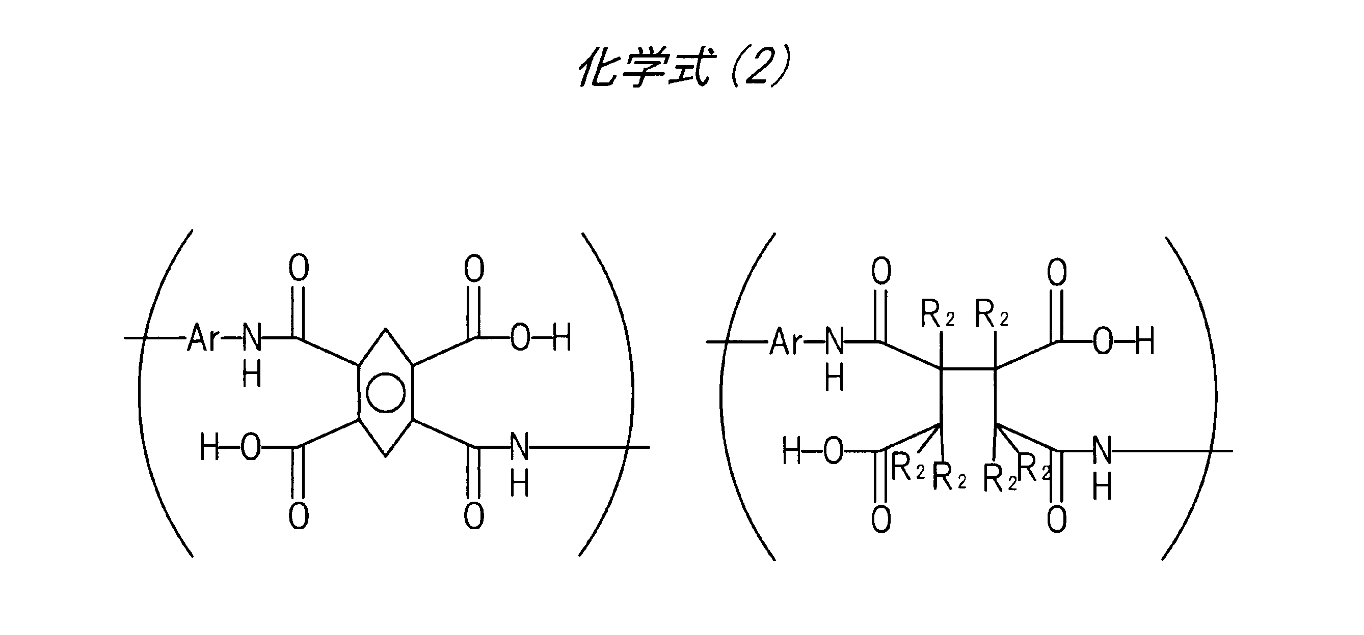
化学式(2)において、R1は、それぞれ独立に炭素数1~8のアルキル基、ヒドロキシル基(OH)、である。R2は、それぞれ独立に水素原子、フッ素原子、塩素原子、臭素原子、フェニル基、炭素数1~6のアルキル基、炭素数1~6のアルコキシ基、ビニル基(-(CH2)m-CH=CH2,m=0,1,2)又はアセチル基(-(CH2)m-C≡CH,m=0,1,2)である。Arは芳香族化合物である。
図6に示す、膜L1Aと膜L1Bとは、互いに異なる材料を主成分とするが、化学式(2)で例示するArの部分に極性の高いジアミンを使用することで、膜L1Aを構成する成分と膜L2Bを構成する成分とを自己整合的に分離することができる。すなわち、化学式(2)で例示するArの部分に極性の高いジアミンを使用することで、ポリアミド酸の表面エネルギーが大きくなるので、配向膜AL1の下地膜である画素電極PE(図4参照)や有機膜15(図4参照)に対する親和性が高くなる。この結果、シクロブタン環を含まないポリアミド酸が下地膜の近くに引き寄せられることになり、膜L1Bには、膜L1Aよりも化学式(2)で示すポリアミド酸が多く分布する。この状態で、イミド化処理を行うと、例えば図6に示すポリイミドPIBのように、主鎖にシクロブタン環を含まないポリイミドが膜L1Bに多く含まれる。一方、図6に示すポリイミドPIA1のように、主鎖にシクロブタン環を含むポリイミドは、膜L1Aに多く分布する。
上記では、図6に示す、膜L1Aと膜L1Bとに含まれるポリイミドの分布について説明したが、膜L2Aと膜L2Bとに含まれるポリイミドの分布、および膜L3Aと膜L3Bとに含まれるポリイミドの分布についても同様である。
図6に示すように、表示装置DSP1の場合、配向膜AL1の膜L1Aの材料は、膜L2Aの材料と同じである。ただし、変形例として配向膜AL1の膜L1Aの材料と膜L2Aの材料とが互いに異なっていても良い。例えば、図7に示す表示装置DSP2の場合、膜L2Aの材料として無置換のシクロブタン骨格を有するポリイミドPIA2を主成分として有する。図7は、図6に対する変形例である表示装置の配向膜の拡大断面図である。
表示装置DSP2の場合、表示装置DSP1と比較して、膜L2Aの機械的強度を強化できるので、配向膜AL2の剥離をさらに抑制できる。一方、領域DA2の配向特性を向上させる観点からは、表示装置DSP1のように、配向膜AL1の膜L1Aの材料が、膜L1Bの材料と同じであることが好ましい。配向膜AL1の膜L1Aの材料は、膜L2Aの材料と異なる。例えば、図7に示す例では、配向膜AL1の膜L1Aの材料は、1,3-ジメチルシクロブタン骨格を有するポリイミドPIA1である。また、配向膜AL1の膜L2Aの材料は、無置換のシクロブタン骨格を有するポリイミドPIA2である。
1,3-ジメチルシクロブタン骨格を有するポリイミドPIA1は、無置換のシクロブタン骨格を有するポリイミドPIA2と比較して紫外線を照射した時にシクロブタン環が開裂し易い。言い換えれば、ポリイミドPIA1は、ポリイミドPIA2と比較して紫外線に対する分解感度が高いので、光配向処理により配向特性を制御し易い。一方、ポリイミドPIA2は、ポリイミドPIA1と比較して紫外線に対する分解感度が低いので、配向膜AL1の膜L2Aは、膜L1Aと比較して、折り曲げられた時の機械的強度が強い。
表示装置DSP2の場合、折り曲げることが想定される領域DA2に、ポリイミドPIA2から成る膜L2Aが配置され、折り曲げることが想定されていない領域DA1には、ポリイミドPIA1から成る膜L1Aが配置される。この場合、領域DA1に配置される配向膜AL1の膜L1Aは、領域DA2に配置される配向膜AL1の膜L2Aよりも良好な配向特性が得られるので、表示品質を向上させることができる。一方、領域DA2には、折り曲げに対する機械的強度が強い膜L2Aが配置されるので、折り曲げることによる配向膜AL1の剥離を抑制できる。この結果、配向膜AL1が剥離した屑により領域DA2の表示品質が低下することを抑制できる。
ところで、図7に示すように、膜L1Aに含まれるポリイミドと、膜L2Aに含まれるポリイミドとが互いに異なる種類のポリイミドになるようにするためには、各領域にポリイミドの原料液を塗布する段階において、領域毎に異なる材料を塗布することが好ましい。また、図6に示すように、膜L1Aの厚さと膜L2Aの厚さが異なるようにする場合にも、原料液の塗布段階で、領域毎に配合割合の異なるポリイミド原料を塗布することが好ましい。例えば、表示装置DSP2の製造工程において、領域DA1には、イミド化処理(例えば230℃程度の加熱処理、または触媒を用いた脱水・還化処理)により1,3-ジメチルシクロブタン骨格を有するポリイミドPIA1になるポリアミド酸、およびイミド化処理により、ピロメリッドイミド骨格を有するポリイミドPIBになるポリアミド酸を含む塗布材料が塗布される。また、領域DA2および領域DA3には、イミド化処理により無置換のシクロブタン骨格を有するポリイミドPIA2になるポリアミド酸、およびイミド化処理により、ピロメリッドイミド骨格を有するポリイミドPIBになるポリアミド酸を含む塗布材料が塗布される。上記のように、領域毎に互いに異なる塗布材料を塗布する場合、インクジェット方式により材料を塗布することが好ましい。配向膜AL1の膜L1Aと膜L2Aとを分離する他の方法については、後述する。
(実施の形態2)
図8および図9に示す表示装置DSP3の場合、表示領域DAは、折り曲げることが想定されていない複数の領域DA1を有し、隣り合う領域DA1の間に、折り曲げ可能な領域DA2を備えている。図8は、図1に対する変形例である表示装置の斜視図である。図9は、図8に示す表示装置を広げた時の平面図である。図10は、図9のA-A線に沿った拡大断面図である。
図8および図9に示す表示装置DSP3の場合、表示領域DAは、折り曲げることが想定されていない複数の領域DA1を有し、隣り合う領域DA1の間に、折り曲げ可能な領域DA2を備えている。図8は、図1に対する変形例である表示装置の斜視図である。図9は、図8に示す表示装置を広げた時の平面図である。図10は、図9のA-A線に沿った拡大断面図である。
表示装置DSP3の場合、図8に示すように、表示領域DAを折り畳むことで携帯時のサイズを低減できる。また、表示装置DSP3は、図9に示すように折り畳まれた表示領域DAを広げることで、大画面で映像を視認することができる。なお、図9では図示を省略したが、表示領域DAには、図1に示す表示装置DSP2と同様に、トランジスタTr1(図2参照)を備える複数の画素PX、複数の画素PXに接続される走査線GL、映像信号線SL、共通電極CEなどが配置されている。
表示装置DSP3において、領域DA2は折り曲げられるので、図6に示す表示装置DSP1の場合と同様に、領域DA2が折り曲げられた時に、配向膜AL1(図10参照)の剥離を抑制する必要がある。領域DA2にある配向膜AL1の剥離を抑制する方法として、図7や図6を用いて説明した方法を適用する場合もあるが、本実施の形態では、他の方法について説明する。
図10に示すように、表示装置DSP3は、基板10と配向膜AL1との間にある有機膜15を有する。有機膜15は、図4に示すように、トランジスタTr1を覆う平坦化膜である。表示装置DSP3の場合、領域DA2と重なる位置にある有機膜15の厚さTH1は、領域DA1と重なる位置にある有機膜15の厚さTH2より薄い。配向膜AL1になる塗布液は、塗布する段階では、粘度の低い液状の材料である。このため、被塗布面に凹凸がある場合には、塗布液は凸部よりも凹部に厚く塗布される。この結果、図10に示すように、領域DA2と重なる位置にある配向膜AL1の厚さTH3は、領域DA1と重なる位置にある配向膜AL1の厚さTH4より厚い。
光配向処理を行う場合、紫外線は配向膜AL1の前面AL1f(言い換えれば液晶層LQと接する面)側から照射される。このため、配向膜AL1の厚さが厚くなれば、前面AL1fの反対側の背面までは、紫外線が到達し難い。このため、領域DA2と重なる位置において、配向膜AL1の背面側は、紫外線によって分断されていないポリイミドが多く残る。この結果、領域DA2と重なる位置において、配向膜AL1の強度を強くすることができる。この方法の場合、例えば配向膜AL1の全体が、図7に示すポリイミドPIA1やポリイミドPIA2のように、シクロブタン骨格を有するポリイミドであっても良い。
ただし、領域DA2と重なる位置において、配向膜AL1の強度を強くする観点からは、表示装置DSP3の配向膜AL1は、図6を用いて説明した表示装置DSP1と同様に、シクロブタン環を含まないポリアミド酸をイミド化したポリイミド(例えば図6や図7に示すピロメリットイミド骨格を有するポリイミドPIB)が含まれていることが好ましい。
また、図6に示す表示装置DSP1の場合と同様に、図10に示す表示装置DSP3の配向膜AL1は、領域DA1および領域DA2のそれぞれと重なる位置において、複数膜の構造となっており、液晶層LQに接する膜L1A(図6参照)と膜L2A(図6参照)との厚さを比較すると、配向膜AL1の膜L2Aの厚さは、膜L1Aの厚さより薄いことが好ましい。これにより、領域DA2が折り曲げられた場合でも、配向膜AL1がさらに剥離し難くなる。
また、図7に示す表示装置DSP2の場合と同様に、図10に示す表示装置DSP3の配向膜AL1は、領域DA1に1,3-ジメチルシクロブタン骨格を有するポリイミドPIA1など、ジメチルシクロブタン環を有するポリイミドが多く配置され、領域DA2に無置換のシクロブタン環を有するポリイミドPIA2が多く配置されることが好ましい。表示装置DSP3において、領域DA1と領域DA2とで配向膜の構成材料を異ならせる場合、配向膜AL1の原料となる塗布液を塗布する工程において、領域DA2における単位面積当たりの塗布量を領域DA1における単位面積当たりの塗布量よりも多くする。これにより、図10に示すように、厚さTH3が厚さTH4よりも厚い構造を備え、かつ、領域DA1と領域DA2とで互いに異なる材料から成る配向膜AL1が得られる。
上記した相違点を除き、表示装置DSP3は、図1~図6を用いて説明した表示装置DSP1、または図7に示す表示装置DSP2と同様である。したがって、重複する説明は省略する。なお、本実施の形態の変形例として、図8~図10を用いて説明した技術、例えば、有機膜15の厚さを薄くすることにより折り曲げ可能な領域DA2の機械的強度を向上させる技術を、図1に示す表示装置DSP2や図6に示す表示装置DSP1に適用することができる。
(実施の形態3)
本実施の形態では、配向膜AL1に疎水性の高い膜を接触させることにより、配向膜AL1におけるポリイミドの種類の分布を制御する態様について説明する。図11は、図10に対する変形例である表示装置の拡大断面図である。
本実施の形態では、配向膜AL1に疎水性の高い膜を接触させることにより、配向膜AL1におけるポリイミドの種類の分布を制御する態様について説明する。図11は、図10に対する変形例である表示装置の拡大断面図である。
図11に示す表示装置DSP4は、基板10と配向膜AL1との間にある有機膜15を有する。有機膜15は、図4に示すように、トランジスタTr1を覆う平坦化膜である。また、表示装置DSP4は、有機膜15を覆う無機膜である絶縁膜16を有する。絶縁膜16は、図4に示す複数の画素電極PEと共通電極CEとの間に設けられる無機絶縁膜である。絶縁膜16は、領域DA2と重なる位置に開口部16Hを備える。配向膜AL1は、絶縁膜16の開口部16Hを介して有機膜15に接する。
有機膜15は無機膜である絶縁膜16と比較して疎水性が高い特性を備える。疎水性が高い材料からなる有機膜15と配向膜AL1とが接触する構造の場合、配向膜AL1におけるポリイミドの種類の分布を制御することができる。例えば、既に説明した化学式(1)に示したシクロブタン環を含むポリアミド酸またはポリアミド酸エステルと、化学式(2)に示したシクロブタン環を含まないポリアミド酸を比較すると、化学式(2)に示すポリアミド酸の方が、有機膜15との親和性が高い。このため、これらの化合物と溶媒とが混在する塗布液の状態において、塗布液の一部が疎水性の高い有機膜15に接していると、有機膜15に近い位置に、化学式(2)に示したシクロブタン環を含まないポリアミド酸が集合し易い。この場合、化学式(1)に示すシクロブタン環を含むポリアミド酸は、有機膜15から離れた位置、すなわち、配向膜AL1の前面AL1f側に集まり易い。
本実施の形態によれば、領域DA2と重なる位置において、有機膜15と配向膜AL1とが接触する。このため、配向膜AL1は、領域DA2と重なる位置において、有機膜15との親和性が高い材料ほど下膜(液晶層LQから遠い膜)に集まり易い。したがって、例えば図6に示すように配向膜AL1が膜L2Aと膜L2Bとを備える場合、膜L2Bには、有機膜15に対する親和性の高いポリイミドPIBが多くなり、膜L2Aには、有機膜15に対する親和性の低いポリイミドPIA2が多くなる。
なお、図11に示す例の場合、領域DA2にも画素PX(図1参照)が存在するので、領域DA2には共通電極CEが配置される。ただし、例えば、領域DA2が狭く、領域DA2に画素PXが配置されない場合には、共通電極CEが配置されていなくても良い。例えば図12に示す表示装置DSP5の場合、領域DA2と重なる位置には、図11に示す絶縁膜16および共通電極CEが存在しない。図12は、図11に対する変形例である表示装置の拡大断面図である。表示装置DSP5の場合、領域DA2と重なる位置の全体において、有機膜15と配向膜AL1とが接触する。したがって、図11に示す例と比較して、有機膜15に対する親和性の高い材料が有機膜15側にさらに集まり易い。この結果、膜L2Aには、有機膜15に対する親和性の低いポリイミドPIA1(図6参照)が多くなる。
上記した相違点を除き、表示装置DSP4および表示装置DSP5は、図1~図6を用いて説明した表示装置DSP1、図7に示す表示装置DSP2、または図8~図10に示す表示装置DSP3と同様である。したがって、重複する説明は省略する。なお、本実施の形態で説明した技術を他の実施の形態で説明した技術と組み合わせて適用しても良い。例えば、表示装置DSP4は、図8に示す表示装置DSP3と同様に、表示領域DAを折り畳む方式の表示装置に適用した場合を例示的に取り上げた。ただし、図3に示す表示装置DSP1のように、領域DA1の両隣の領域が折れ曲がるタイプの表示装置に適用しても良い。
(実施の形態4)
本実施の形態では、例えば、図6に示す領域DA1と領域DA2との間に部材が設けられ、この部材により領域DA1の配向膜AL1と領域DA1の配向膜AL1とを分離する実施態様について説明する。図13は、図3に対する変形例である表示装置において、互いに分離された配向膜の境界周辺を拡大して示す拡大断面図である。図14は、図13に示す部分を表示面側から視た拡大平面図である。図14は平面図であるが、部材SW1にハッチングを付して示している。なお、図13および図14に示す表示装置DSP6の全体構造は、例えば図1や図3に示す表示装置DSP1の構造、あるいは、図8や図9に示す表示装置DSP3の構造と同様である。
本実施の形態では、例えば、図6に示す領域DA1と領域DA2との間に部材が設けられ、この部材により領域DA1の配向膜AL1と領域DA1の配向膜AL1とを分離する実施態様について説明する。図13は、図3に対する変形例である表示装置において、互いに分離された配向膜の境界周辺を拡大して示す拡大断面図である。図14は、図13に示す部分を表示面側から視た拡大平面図である。図14は平面図であるが、部材SW1にハッチングを付して示している。なお、図13および図14に示す表示装置DSP6の全体構造は、例えば図1や図3に示す表示装置DSP1の構造、あるいは、図8や図9に示す表示装置DSP3の構造と同様である。
表示装置DSP6は、可撓性を有し、前面(主面、表面)10fに領域DA1および領域DA2を有する基板10と、液晶層LQと、液晶層LQに接し、光分解性がある配向膜AL1と、を備える。基板10は、領域DA2において折り曲げ可能である。配向膜AL1は、領域DA1と重なる配向膜AL11と、領域DA2と重なる配向膜AL12と、を含む。また、図14に示すように、平面視において、配向膜AL11と配向膜AL12との間には、配向膜AL11と配向膜AL12とを分離する部材SW1が配置される。
部材SW1は、例えば樹脂などの有機材料からなる構造物であって、領域DA1と領域DA2の境界に沿って、Y方向に延びる。部材SW1の頂部(前面)SWfは、配向膜AL1の前面AL1fより高い位置(図3に示す基板20側)にある。言い換えれば、基板10から部材SW1の頂部SWfまでの距離は、基板10から配向膜AL1の前面AL1fまでの距離より長い。さらに言い換えれば、部材SW1は、配向膜AL1の前面AL1fから突出している。このため、部材SW1は、配向膜AL11と配向膜AL12とを分離する分離壁として機能する。
部材SW1のように、領域DA1と領域DA2との境界に、配向膜AL1を分離する分離壁として機能する部材を配置することにより、配向膜AL11と、配向膜AL12との材料を異なる材料で形成し易い。例えば、表示装置DSP6の製造方法では、配向膜AL1の材料を塗布する前に、部材SW1を形成する。その後、領域DA1と重なる位置に配向膜AL11の材料を塗布し、領域DA2と重なる位置に配向膜AL12の材料を塗布する。その後、塗布材料に含まれる溶媒を除去する乾燥処理を施した後、230℃程度に加熱して、ポリイミドの原料に対してイミド化処理を行う。その後、イミド化された配向膜AL1に紫外線を照射することにより、光配向処理を施す。表示装置DSP6の場合、配向膜AL11と配向膜AL12とを確実に分離できるので、配向膜AL11と配向膜AL12との構成材料が互いに異なる場合に、配向膜AL11と配向膜AL12との境界部分での材料の混合を抑制できる。例えば図6に示す表示装置DSP1や図7に示す表示装置DSP2の場合、領域DA1と領域DA2にそれぞれ異なる塗布材料を塗布する必要がある。この場合に表示装置DSP6のように、領域DA1と領域DA2との境界に部材SW1を配置する方法が有効である。
また、図13に示すように、配向膜AL11、配向膜AL12、および部材SW1のそれぞれは、同一の下地膜上に形成されている。図13に示す例の場合、配向膜AL11、配向膜AL12、および部材SW1のそれぞれは、無機絶縁膜である絶縁膜16上に形成されている。このように、配向膜AL11、配向膜AL12、および部材SW1のそれぞれが同一の下地膜上に形成されている場合、配向膜AL11と配向膜AL12とを確実に分離することができる。
ところで、図13に示す例では、配向膜AL11と配向膜AL12とを分離する分離壁の例として、配向膜AL1の前面AL1fから突出する部材SW1を取り上げて説明した。ただし、配向膜AL11と配向膜AL12との間に配置される分離壁の例には種々の変形例がある。例えば、図15に示す表示装置DSP7の場合、配向膜AL11と配向膜AL12とを分離する部材SW2の頂部SWfは、配向膜AL1の前面AL1fと連なっている。言い換えれば、部材SW2の頂部SWfと配向膜AL1の前面AL1fとは、互いに同程度の高さに位置している。図15は、図13に対する変形例である表示装置の拡大断面図である。なお、図示は省略するが、図15に示す部材SW2は、図14に示す部材SW1と同様に、領域DA1と領域DA2との境界に沿ってY方向に延びる。
図15に示す部材SW2は、配向膜AL1に含まれるワニス材料に対する撥液性を備える。撥液現象は例えば以下の原理により発生する。配向膜AL11の原料および配向膜AL12の原料は、それぞれ溶媒を含むワニス材料である。部材SW2は、例えば、原料塗布液を領域DA1と領域DA2との境界に塗布した後、加熱することで硬化させることにより形成される。硬化後の部材SW2は、このワニス材料を含む溶媒に対して、相溶性が悪い(溶け難い)特性を備える。この場合、部材SW1と配向膜AL1との接触界面では、両者が互いに反発して分離する(言い換えれば撥液する)。
表示装置DSP7の場合、上記した撥液現象を利用することにより、配向膜AL11と配向膜AL12とが分離される。この場合、図13に示す部材SW1のように部材SW1の高さ(厚さ)を高く(厚く)する必要が無いので、頂部SWfの高さを配向膜AL1の前面AL1fの高さと同程度にすることができる。部材SW2のように頂部SWfの高さを低くできれば、部材SW2の頂部と接触することにより、配向膜AL1や配向膜AL2(図4参照)が損傷することを抑制できる。
上記した相違点を除き、表示装置DSP6および表示装置DSP7は、図1~図6を用いて説明した表示装置DSP1、図7に示す表示装置DSP2、または図8~図10に示す表示装置DSP3と同様である。したがって、重複する説明は省略する。なお、本実施の形態で説明した技術を他の実施の形態で説明した技術と組み合わせて適用しても良い。
(実施の形態5)
本実施の形態では、例えば、折り曲げ可能な領域に配向膜の下地膜から突出する部材(スペーサ部材)が設けられ、部材上の配向膜の厚さが薄くなる、あるいは部材上には配向膜が配置されない実施態様について説明する。図16は、図14に対する変形例である表示装置の拡大平面図である。図17は、図16のA-A線に沿った拡大断面図である。なお、図16および図17に示す表示装置DSP8の全体構造は、例えば図8や図9に示す表示装置DSP3の構造と同様である。
本実施の形態では、例えば、折り曲げ可能な領域に配向膜の下地膜から突出する部材(スペーサ部材)が設けられ、部材上の配向膜の厚さが薄くなる、あるいは部材上には配向膜が配置されない実施態様について説明する。図16は、図14に対する変形例である表示装置の拡大平面図である。図17は、図16のA-A線に沿った拡大断面図である。なお、図16および図17に示す表示装置DSP8の全体構造は、例えば図8や図9に示す表示装置DSP3の構造と同様である。
表示装置DSP8は、可撓性を有し、前面(主面、表面)10fに領域DA1、領域DA2、および領域DA3を有する基板10と、液晶層LQと、液晶層LQに接し、光分解性がある配向膜AL1と、を備える。基板10は、領域DA2において折り曲げ可能である。領域DA2は、領域DA1と領域DA3との間にある。領域DA1および領域DA3は、折り曲げることを想定していない領域である。図17に示す例では、領域DA2には、配向膜AL1の下地膜である絶縁膜16から液晶層LQの方向に向かって突出する部材PSBが配置される。図16に示すように、部材PSBは、領域DA2の延在方向に沿って、Y方向に延びる。
表示装置DSP8の場合、領域DA2に部材PSBが設けられているので、部材PSB上、すなわち、領域DA2と重なる位置における配向膜AL1の厚さが、領域DA1および領域DA3と重なる位置における配向膜AL1の厚さより薄い。また、部材PSBの高さによっては、部材PSB上には配向膜AL1が配置されない場合もある。このように、折り曲げ可能な領域である領域DA2において、配向膜AL1が殆ど無い場合、領域DA2を折り曲げたとしても、配向膜AL1が削られることを考慮する必要が無い。したがって、配向膜AL1が削れた屑により液晶層LQの液晶分子の配向が阻害されることを抑制できる。また、領域DA2の曲げ方向が予め想定されている場合には、図17に示すように部材PSBの頂部に複数の溝が形成されていることが好ましい。これにより、領域DA2で折り曲げることが容易になる。
上記した相違点を除き、表示装置DSP8は、図1~図6を用いて説明した表示装置DSP1、図7に示す表示装置DSP2、または図8~図10に示す表示装置DSP3と同様である。したがって、重複する説明は省略する。なお、本実施の形態で説明した技術を他の実施の形態で説明した技術と組み合わせて適用しても良い。
(実施の形態6)
本実施の形態では、折り曲げ可能な領域において、配向膜AL1に加わる物理的なストレスを低減することにより、折り曲げ可能な領域における配向膜AL1の剥離を抑制する態様について説明する。図18は、図1に対する変形例である表示装置の拡大平面図である。図19は、図18のA-A線に沿った拡大断面図である。また、図20は、図18に対する変形例である表示装置の拡大平面図である。図18および図20では、円錐台形を成すスペーサ部材PS2の頂部の輪郭を点線で示している。表示装置DSP9の全体構造は、例えば図1や図3に示す表示装置DSP1の構造、あるいは、図8や図9に示す表示装置DSP3の構造と同様である。
本実施の形態では、折り曲げ可能な領域において、配向膜AL1に加わる物理的なストレスを低減することにより、折り曲げ可能な領域における配向膜AL1の剥離を抑制する態様について説明する。図18は、図1に対する変形例である表示装置の拡大平面図である。図19は、図18のA-A線に沿った拡大断面図である。また、図20は、図18に対する変形例である表示装置の拡大平面図である。図18および図20では、円錐台形を成すスペーサ部材PS2の頂部の輪郭を点線で示している。表示装置DSP9の全体構造は、例えば図1や図3に示す表示装置DSP1の構造、あるいは、図8や図9に示す表示装置DSP3の構造と同様である。
表示装置DSP9は、領域DA1および領域DA2において、基板10と対向し、かつ基板10と離間する基板20(図19参照)を有する。また、表示装置DSP9は、領域DA1と重なる位置、および領域DA2と重なる位置のそれぞれにおいて、基板10と2基板20との間に配置される複数のスペーサ部材PSを有する。
液晶表示装置の場合、液晶層LQの厚さが極端に小さくなると、表示品質が低下するので、表示装置DSP9のように、基板10と基板20との間に、液晶層LQの厚さを維持する複数のスペーサ部材PSが配置されていることが好ましい。図19に示す例では、複数のスペーサ部材PSのそれぞれは、基板20側に固定されている。ただし、スペーサ部材PSが、基板10および基板20のうちいずれかに固定されていれば良く、図19の他、種々の変形例がある。例えば、複数のスペーサ部材PSのそれぞれが基板10側に固定されていても良い。あるいは、基板10側に固定される複数のスペーサ部材PSと、基板20側に固定される複数のスペーサ部材PSとが混在していても良い。
複数のスペーサ部材PSには、領域DA1と重なる位置に配置される複数のスペーサ部材PS1と、領域DA2と重なる位置に配置される複数のスペーサ部材PS2と、を含む。スペーサ部材PSは、上記したように液晶層LQの厚さ、別の表現をすれば、基板10と基板20との離間距離が極端に小さくなることを抑制する部材である。このため、表示装置DSP9に外力が印加され、液晶層LQの厚さが一時的に薄くなった場合、スペーサ部材PSの頂部が配向膜AL1に接触する。この時、スペーサ部材PS接触したことにより、配向膜AL1の一部分が剥離することを抑制することが好ましい。特に、折り曲げて使用することが想定されている領域DA2では、スペーサ部材PS2と配向膜AL2とが接触する可能性が高い。
そこで、表示装置DSP9の場合、領域DA2にスペーサ部材PS2を高密度で配置することにより、各スペーサ部材PS2が配向膜AL1に接触した時に生じる応力を低減している。図18に示すように、表示装置DSP9の場合、領域DA2と重なる位置にある複数のスペーサ部材PS2の配置密度は、領域DA1と重なる位置にあるスペーサ部材PS1の配置密度よりも高い。言い換えれば、平面視において、隣り合うスペーサ部材PS2の離間距離は、隣り合うスペーサ部材PS1の離間距離より短い。この場合、領域DA2を折り曲げた時に、スペーサ部材PS2と配向膜AL1とが接触するが、配向膜AL2に局所的に印加される力は小さくなるので、配向膜AL1がスペーサ部材PS2に削られて剥離が生じることを抑制できる。
また、スペーサ部材PS2により、配向膜AL1が削られることを抑制する観点から、図20に示す表示装置DSP6のように、複数のスペーサ部材PS2の頂部の面積を大きくすることが好ましい。図20に示す表示装置DSP6の場合、DA2領域と重なる位置にあるスペーサ部材PS2の頂部の幅PSW2が、領域DA1と重なる位置にあるスペーサ部材PS1の頂部の幅PSW1より広い点で、図18に示す表示装置DSP9と相違する。言い換えれば、表示装置DSP6が備えるスペーサ部材PS2の頂部の面積は、スペーサ部材PS1の頂部の面積より大きい。
複数のスペーサ部材PSのそれぞれは、円錐台、あるいは角錐台などの形状を備える。図18および図20に示す例では、スペーサ部材PSの形状は、円錐台である。スペーサ部材PSと配向膜AL1とが接触する場合、円錐台や角錐台を成すスペーサ部材PSの頂部が配向膜AL1と接触する。
複数のスペーサ部材PS2のそれぞれの頂部の面積が大きい場合、スペーサ部材PS2の頂部と配向膜AL1との接触面積が大きくなる。この結果、配向膜AL1の一部に集中的な力が印加されることを抑制できるので、配向膜AL1がスペーサ部材PS2に削られて剥離が生じることを抑制できる。
上記した相違点を除き、表示装置DSP9は、上述した表示装置DSP1~表示装置DSP8のいずれかと同様である。したがって、重複する説明は省略する。なお、本実施の形態で説明した技術を他の実施の形態で説明した技術と組み合わせて適用しても良い。
上記の通り説明した技術は、既に説明した種々の変形例の他、さらに別の変形例に適用可能である。例えば上記では、図3に示すように、表示領域DAのうち、領域DA1の両隣にある領域DA2、DA3のそれぞれが湾曲するように折り曲げられる例、および、図8に示すように、領域DA2に沿って折り畳むことが可能な表示装置の例を取り上げて説明した。折り曲げの方法および、折り曲げ可能な領域のレイアウトには上記の他、種々の変形例がある。
図16および図17を用いて説明した表示装置DSP8の構造は以下のように表現できる。
可撓性を有し、表面に第1領域、第2領域、および第3領域を有する第1基板と、
液晶層と、
前記液晶層に接し、光分解性がある配向膜と、
を備え、
前記第1基板は、前記第2領域で折り曲げ可能であり、
前記第2領域は、前記第1領域と前記第3領域との間にあり、
前記第2領域には、前記配向膜の下地膜から前記第1液晶層の方向に向かって突出するスペーサ部材が配置される、表示装置。
液晶層と、
前記液晶層に接し、光分解性がある配向膜と、
を備え、
前記第1基板は、前記第2領域で折り曲げ可能であり、
前記第2領域は、前記第1領域と前記第3領域との間にあり、
前記第2領域には、前記配向膜の下地膜から前記第1液晶層の方向に向かって突出するスペーサ部材が配置される、表示装置。
本発明の思想の範疇において、当業者であれば、各種の変更例及び修正例に想到し得るものであり、それら変更例及び修正例についても本発明の範囲に属するものと了解される。例えば、前述の各実施形態に対して、当業者が適宜、構成要素の追加、削除若しくは設計変更を行ったもの、または、工程の追加、省略若しくは条件変更を行ったものも、本発明の要旨を備えている限り、本発明の範囲に含まれる。
本発明は、表示装置や表示装置が組み込まれた電子機器に利用可能である。
10,20 基板
10b,20b 背面(主面、裏面)
10f,20f 前面(主面、表面)
11,12,13,14,16,OC1 絶縁膜
15 有機膜(平坦化膜、有機絶縁膜)
16H 開口部
AL1,AL11,AL12,AL2 配向膜
AL1f 前面
ALP 配向軸
BM 遮光膜
BND シール材
CD 共通電極駆動回路
CDP 導体パターン
CE 共通電極
CF カラーフィルタ
DA 表示領域
DA1 領域(第1領域)
DA2 領域(第2領域)
DA3 領域(第3領域)
DE ドレイン電極
DSP1,DSP2,DSP3,DSP4,DSP5,DSP6,DSP7,DSP8 表示装置
GD 走査線駆動回路(ゲート駆動回路)
GE ゲート電極
GL 走査線(ゲート線)
Gsi 走査信号
L1A,L1B,L2A,L2B,L3A,L3B 層(部分)
LQ 液晶層
PE 画素電極
PFR 周辺領域
PI1,PIA1,PIA2,PIB ポリイミド
PI2 組成物
PS,PS1,PS2 スペーサ部材
PX 画素
SCR 半導体領域(半導体層)
SD 信号線駆動回路
SE ソース電極
SL 映像信号線(ソース線)
Spic 映像信号
PSB,SW1,SW2 部材
PSW1,PSW2 幅
SUB1,SUB2 基板
SWf 頂部(前面)
Tr1 トランジスタ
UVP 偏光軸
10b,20b 背面(主面、裏面)
10f,20f 前面(主面、表面)
11,12,13,14,16,OC1 絶縁膜
15 有機膜(平坦化膜、有機絶縁膜)
16H 開口部
AL1,AL11,AL12,AL2 配向膜
AL1f 前面
ALP 配向軸
BM 遮光膜
BND シール材
CD 共通電極駆動回路
CDP 導体パターン
CE 共通電極
CF カラーフィルタ
DA 表示領域
DA1 領域(第1領域)
DA2 領域(第2領域)
DA3 領域(第3領域)
DE ドレイン電極
DSP1,DSP2,DSP3,DSP4,DSP5,DSP6,DSP7,DSP8 表示装置
GD 走査線駆動回路(ゲート駆動回路)
GE ゲート電極
GL 走査線(ゲート線)
Gsi 走査信号
L1A,L1B,L2A,L2B,L3A,L3B 層(部分)
LQ 液晶層
PE 画素電極
PFR 周辺領域
PI1,PIA1,PIA2,PIB ポリイミド
PI2 組成物
PS,PS1,PS2 スペーサ部材
PX 画素
SCR 半導体領域(半導体層)
SD 信号線駆動回路
SE ソース電極
SL 映像信号線(ソース線)
Spic 映像信号
PSB,SW1,SW2 部材
PSW1,PSW2 幅
SUB1,SUB2 基板
SWf 頂部(前面)
Tr1 トランジスタ
UVP 偏光軸
Claims (13)
- 可撓性を有し、表面に第1領域および第2領域を有する第1基板と、
液晶層と、
前記液晶層に接し、光分解性がある配向膜と、
を備え、
前記第1基板は、前記第2領域で折り曲げ可能であり、
前記配向膜は、前記液晶層に接し、光分解性を備える材料を含む第1膜を含み、
前記第2領域にある前記第1膜の厚さは、前記第1領域にある前記第1膜の厚さより薄い、表示装置。 - 前記第1基板上にある第1トランジスタと、
前記第1基板と前記配向膜との間にあり、前記第1トランジスタを覆う第1有機膜と、
をさらに備え、
前記第2領域にある前記第1有機膜の厚さは、前記第1領域にある前記第1有機膜の厚さより薄い、請求項1に記載の表示装置。 - 前記配向膜は、前記第1膜と前記第1基板との間にある第2膜をさらに有し、
前記第2領域にある前記第2膜の厚さは、前記第1領域にある前記第2膜の厚さより厚い、請求項1または2に記載の表示装置。 - 可撓性を有し、表面に第1領域および第2領域を有する第1基板と、
液晶層と、
前記液晶層に接する配向膜と、
前記第1基板上にある第1トランジスタと、
前記第1基板と前記配向膜との間にあり、前記第1トランジスタを覆う第1有機膜と、
を備え、
前記第1基板は、前記第2領域で折り曲げ可能であり、
前記第2領域にある前記第1有機膜の厚さは、前記第1領域にある前記第1有機膜の厚さより薄い、表示装置。 - 前記第1有機膜は、前記配向膜と接する、請求項4に記載の表示装置。
- 前記第1有機膜を覆う第1無機膜、をさらに備え、
前記第1無機膜は、前記第2領域に開口部を備え、
前記配向膜は前記第2領域において、前記第1無機膜の開口部を介して前記第1有機膜に接する、請求項2または5に記載の表示装置。 - 可撓性を有し、表面に第1領域および第2領域を有する第1基板と、
液晶層と、
前記液晶層に接し、光分解性がある配向膜と、
を備え、
前記第1基板は、前記第2領域で折り曲げ可能であり、
前記配向膜は、前記第1領域と重なる位置にある第1配向膜と、前記第2領域と重なる位置にある第2配向膜と、を含み、
平面視において、前記第1配向膜と前記第2配向膜との間には、前記第1配向膜と前記第2配向膜とを分離する第1部材が配置される、表示装置。 - 前記第1部材は、前記配向膜を形成するためのワニス材料に対する撥液性を備える、請求項7に記載の表示装置。
- 前記第1配向膜、前記第2配向膜、および前記第1部材のそれぞれは、同一の下地膜上に形成される、請求項7または8に記載の表示装置。
- 前記第1領域および前記第2領域において、前記第1基板と対向し、かつ前記第1基板と離間する第2基板と、
前記第1領域と重なる位置、および前記第2領域と重なる位置のそれぞれにおいて、前記第1基板と前記第2基板との間に配置される複数のスペーサ部材と、
をさらに備え、
前記第2領域と重なる位置にある第2スペーサ部材の配置密度は、前記第1領域と重なる位置にある第1スペーサ部材の配置密度よりも高い、請求項5,7,および8 のいずれか1項に記載の表示装置。 - 前記第1領域および前記第2領域において、前記第1基板と対向し、かつ前記第1基板と離間する第2基板と、
前記第1領域と重なる位置、および前記第2領域と重なる位置のそれぞれにおいて、前記第1基板と前記第2基板との間に配置される複数のスペーサ部材と、
をさらに備え、
前記第2領域と重なる位置にある第2スペーサ部材の頂部の幅は、前記第1領域と重なる位置にある第1スペーサ部材の頂部の幅より広い、請求項1,2,4,5,7,および8 のいずれか1項に記載の表示装置。 - 前記配向膜は、前記液晶層に接し、光分解性を備える材料を含む第1膜と、前記第1膜と前記第1基板との間にある第2膜と、を有し、
前記第1膜は、シクロブタン環を有するポリイミド材料を含む、請求項1,2,4,5,7,および8 のいずれか1項に記載の表示装置。 - 前記第2膜は、ピロメリットイミド骨格を有するポリイミド材料を含む、請求項12に記載の表示装置。
Applications Claiming Priority (2)
| Application Number | Priority Date | Filing Date | Title |
|---|---|---|---|
| JP2018120465A JP7158914B2 (ja) | 2018-06-26 | 2018-06-26 | 表示装置 |
| JP2018-120465 | 2018-06-26 |
Publications (1)
| Publication Number | Publication Date |
|---|---|
| WO2020003659A1 true WO2020003659A1 (ja) | 2020-01-02 |
Family
ID=68986953
Family Applications (1)
| Application Number | Title | Priority Date | Filing Date |
|---|---|---|---|
| PCT/JP2019/012572 Ceased WO2020003659A1 (ja) | 2018-06-26 | 2019-03-25 | 表示装置 |
Country Status (2)
| Country | Link |
|---|---|
| JP (1) | JP7158914B2 (ja) |
| WO (1) | WO2020003659A1 (ja) |
Citations (3)
| Publication number | Priority date | Publication date | Assignee | Title |
|---|---|---|---|---|
| JP2009115933A (ja) * | 2007-11-05 | 2009-05-28 | Mitsubishi Electric Corp | 液晶表示装置及びその製造方法 |
| WO2015122032A1 (ja) * | 2014-02-14 | 2015-08-20 | 旭化成イーマテリアルズ株式会社 | ポリイミド前駆体及びそれを含有する樹脂組成物 |
| JP2018049193A (ja) * | 2016-09-23 | 2018-03-29 | 株式会社ジャパンディスプレイ | 表示装置 |
Family Cites Families (1)
| Publication number | Priority date | Publication date | Assignee | Title |
|---|---|---|---|---|
| US10211416B2 (en) | 2016-12-28 | 2019-02-19 | Shanghai Tianma AM-OLED Co., Ltd. | Flexible display panel, fabrication method, and flexible display apparatus |
-
2018
- 2018-06-26 JP JP2018120465A patent/JP7158914B2/ja active Active
-
2019
- 2019-03-25 WO PCT/JP2019/012572 patent/WO2020003659A1/ja not_active Ceased
Patent Citations (3)
| Publication number | Priority date | Publication date | Assignee | Title |
|---|---|---|---|---|
| JP2009115933A (ja) * | 2007-11-05 | 2009-05-28 | Mitsubishi Electric Corp | 液晶表示装置及びその製造方法 |
| WO2015122032A1 (ja) * | 2014-02-14 | 2015-08-20 | 旭化成イーマテリアルズ株式会社 | ポリイミド前駆体及びそれを含有する樹脂組成物 |
| JP2018049193A (ja) * | 2016-09-23 | 2018-03-29 | 株式会社ジャパンディスプレイ | 表示装置 |
Also Published As
| Publication number | Publication date |
|---|---|
| JP2020003549A (ja) | 2020-01-09 |
| JP7158914B2 (ja) | 2022-10-24 |
Similar Documents
| Publication | Publication Date | Title |
|---|---|---|
| JP5285729B2 (ja) | 液晶表示装置 | |
| CN103091914B (zh) | 边缘场切换液晶显示器装置及其制造方法 | |
| KR101350709B1 (ko) | 표시패널 및 표시기판의 제조 방법 | |
| KR101182229B1 (ko) | 액정 표시 패널 및 그의 형성 방법 | |
| JP6522182B1 (ja) | 液晶表示装置 | |
| CN1991541A (zh) | 液晶显示器件及其制造方法 | |
| CN1716015A (zh) | 防止像素区外的区域漏光的cot液晶显示器及其制造法 | |
| CN1577015A (zh) | 共平面开关型液晶显示装置及其制造方法 | |
| JP5806383B2 (ja) | 液晶表示装置 | |
| CN108508661B (zh) | 液晶显示面板及液晶显示装置 | |
| WO2012165221A1 (ja) | 液晶表示装置およびその製造方法 | |
| US10649253B2 (en) | Display panel and manufacturing method of display panel | |
| JP7261595B2 (ja) | 表示装置 | |
| JP2015141299A (ja) | 液晶表示装置 | |
| JP7158914B2 (ja) | 表示装置 | |
| US11474387B2 (en) | Display apparatus | |
| US20140063394A1 (en) | Liquid crystal display device and method of manufacturing the same | |
| JP2013134317A (ja) | 液晶表示装置 | |
| WO2019187452A1 (ja) | 電気光学装置 | |
| JP2020126109A (ja) | 電気光学装置 | |
| KR101881119B1 (ko) | 액정표시장치용 어레이 기판 | |
| KR20120132853A (ko) | 박막 트랜지스터 기판 및 이의 제조 방법 | |
| KR20130020067A (ko) | 표시장치 및 그 제조방법 | |
| JP2008046631A (ja) | Lcdパネルの半透過型画素構造とその製造方法 | |
| CN210401940U (zh) | 显示装置 |
Legal Events
| Date | Code | Title | Description |
|---|---|---|---|
| 121 | Ep: the epo has been informed by wipo that ep was designated in this application |
Ref document number: 19826891 Country of ref document: EP Kind code of ref document: A1 |
|
| NENP | Non-entry into the national phase |
Ref country code: DE |
|
| 122 | Ep: pct application non-entry in european phase |
Ref document number: 19826891 Country of ref document: EP Kind code of ref document: A1 |