WO2019239693A1 - 固体撮像装置及び電子機器 - Google Patents
固体撮像装置及び電子機器 Download PDFInfo
- Publication number
- WO2019239693A1 WO2019239693A1 PCT/JP2019/015164 JP2019015164W WO2019239693A1 WO 2019239693 A1 WO2019239693 A1 WO 2019239693A1 JP 2019015164 W JP2019015164 W JP 2019015164W WO 2019239693 A1 WO2019239693 A1 WO 2019239693A1
- Authority
- WO
- WIPO (PCT)
- Prior art keywords
- solid
- state imaging
- imaging device
- lens group
- light guide
- Prior art date
- Legal status (The legal status is an assumption and is not a legal conclusion. Google has not performed a legal analysis and makes no representation as to the accuracy of the status listed.)
- Ceased
Links
Images








Classifications
-
- G—PHYSICS
- G02—OPTICS
- G02B—OPTICAL ELEMENTS, SYSTEMS OR APPARATUS
- G02B13/00—Optical objectives specially designed for the purposes specified below
-
- H—ELECTRICITY
- H04—ELECTRIC COMMUNICATION TECHNIQUE
- H04N—PICTORIAL COMMUNICATION, e.g. TELEVISION
- H04N25/00—Circuitry of solid-state image sensors [SSIS]; Control thereof
- H04N25/70—SSIS architectures; Circuits associated therewith
-
- H—ELECTRICITY
- H10—SEMICONDUCTOR DEVICES; ELECTRIC SOLID-STATE DEVICES NOT OTHERWISE PROVIDED FOR
- H10F—INORGANIC SEMICONDUCTOR DEVICES SENSITIVE TO INFRARED RADIATION, LIGHT, ELECTROMAGNETIC RADIATION OF SHORTER WAVELENGTH OR CORPUSCULAR RADIATION
- H10F39/00—Integrated devices, or assemblies of multiple devices, comprising at least one element covered by group H10F30/00, e.g. radiation detectors comprising photodiode arrays
- H10F39/10—Integrated devices
- H10F39/12—Image sensors
Definitions
- the present disclosure relates to a solid-state imaging device and an electronic apparatus.
- an imaging lens objective lens
- a plurality of solid-state imaging elements are arranged close to each other in a matrix on one imaging element plane.
- the solid-state imaging device can obtain an image of a subject by combining the imaging information acquired by each of the plurality of solid-state imaging elements into one.
- each solid-state imaging element is required to detect incident light from a predetermined range without overlapping each other, and obtain imaging information related to the detected incident light.
- Each pixel including the image sensor preferably has a narrow angle of view that does not overlap each other.
- Patent Document 1 two pinholes are provided between the microlens and the solid-state imaging device, and in the following Patent Document 2, one pinhole is provided. Is provided.
- Patent Documents 1 and 2 by limiting the range of incident light that can be detected by each solid-state imaging device by the pinhole, the angle of view of each pixel is avoided from overlapping each other.
- the present disclosure proposes a new and improved solid-state imaging device and electronic apparatus that can increase the use efficiency of incident light while avoiding overlapping of the angle of view of adjacent pixels.
- the image sensor includes a plurality of pixels arranged in a matrix on the image sensor surface, each pixel including at least one solid-state image sensor and at least one solid-state image sensor provided on the subject side.
- a light guide unit, and the light guide unit has a first transparent body and a positive optical power from the subject side toward the solid-state image sensor side along the light guide direction of the light guide unit.
- a solid-state imaging device that sequentially includes a first lens group having a light-shielding part having an opening, and a second lens group having a positive optical power.
- an electronic apparatus including a solid-state imaging device having a plurality of pixels arranged in a matrix on the imaging element surface, wherein each pixel includes at least one solid-state imaging element and the solid state At least one light guide provided on the subject side of the image sensor, and the light guide from the subject side toward the solid-state image sensor side along the light guide direction of the light guide.
- an electronic device that sequentially includes a first transparent body, a first lens group having a positive optical power, a light-shielding portion having an opening, and a second lens group having a positive optical power Is done.
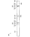
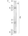
- FIG. 2 is a schematic diagram of a pixel 10 according to the first embodiment of the present disclosure.
- FIG. FIG. 2 is a schematic diagram illustrating the progress of incident light in the light guide unit 200 illustrated in FIG. 1.
- 1 is a schematic cross-sectional view of a solid-state imaging device 1 according to a first embodiment of the present disclosure.
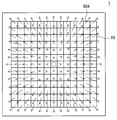
- 2 is a schematic plan view of the solid-state imaging device 1 according to the first embodiment of the present disclosure.
- FIG. It is a mimetic diagram of the section of solid imaging device 1a concerning a 2nd embodiment of this indication. It is a mimetic diagram of the section of solid imaging device 1b concerning a 3rd embodiment of this indication. It is a mimetic diagram of the section of solid imaging device 1c concerning a 4th embodiment of this indication.
- a plurality of components having substantially the same or similar functional configuration may be distinguished by adding different numbers after the same reference numerals. However, when it is not necessary to particularly distinguish each of a plurality of constituent elements having substantially the same or similar functional configuration, only the same reference numerals are given.
- similar components in different embodiments may be distinguished by attaching different alphabets after the same reference numerals. However, if it is not necessary to distinguish each similar component, only the same reference numerals are given.
- positive power and negative power used for a lens means the strength of bending a light beam by the lens, for example, adjusting the refractive index and curvature of the lens. Thus, the power changes. Further, in the following description, “positive power” of the lens power means the strength of bending in the light condensing direction (inside the lens), while “negative power” means light. This means the strength to bend in the direction of divergence (outside of the lens).
- the chief ray means incident light that passes through the center of the optical system (pixel 10 described later).
- the upper ray means incident light that passes through an edge located above the central axis of the optical system and forms an image on the solid-state imaging device, and the lower ray is lower than the central axis of the optical system. It means incident light that passes through the lower edge and forms an image on the solid-state imaging device.
- angle of view means a range (angle) of an image detected by each pixel 10.
- FIG. 11 is a schematic diagram of the pixel 20 according to the comparative example.
- the comparative example means a configuration of a solid-state imaging device that the inventor has studied before making embodiments of the present disclosure, and specifically, a configuration that is not a Kepler type optical system. Means.
- a solid-state imaging device using a microlens having a planar size of the same level as the unit pixel of the solid-state imaging device instead of the imaging lens (objective lens) for example, in Patent Documents 1 and 2 above, Mention may be made of the disclosed apparatus.
- a plurality of solid-state imaging elements are arranged close to each other in a matrix on one imaging element plane.
- the solid-state imaging device can obtain an image of a subject by combining the imaging information acquired by each of the plurality of solid-state imaging elements into one.
- the solid-state imaging device is required to detect incident light from a narrow predetermined range from the subject side and obtain imaging information related to the detected incident light without the solid-state imaging elements overlapping each other. Therefore, each pixel including each solid-state imaging device is configured to have a narrow angle of view that does not overlap each other.
- the solid-state imaging device according to the comparative example has a plurality of pixels 20 close to each other as shown in FIG.
- Each pixel 20 includes solid-state imaging devices 300a and 300b and a light guide unit 202 that guides light from the subject side to each solid-state imaging device 300a and 300b.
- the left side is the subject side.
- the solid-state imaging device 300a includes not only incident light 600a indicated by a solid line (shown by three lines of a principal ray and an upper ray and a lower ray sandwiching the principal ray), but also a two-dot broken line.
- the incident light 600b (shown by three lines of a principal ray and an upper ray and a lower ray sandwiching the principal ray) is also detected.
- the incident light 600b has a chief ray inclined about 5 degrees with respect to the chief ray of the incident light 600a.
- the incident light 600a reaches the solid-state image sensor 300a without protruding from the light guide unit 202 of the solid-state image sensor 300a.
- the incident light 600b passes through the light guide unit 202 of the solid-state imaging device 300b in which the lower light beam approaches, and reaches the solid-state imaging device 300a.
- the lower ray of the incident light 600b is incident light that should be detected by the adjacent solid-state imaging device 300b. In this way, when the solid-state image sensor 300a detects incident light that should be detected by the solid-state image sensor 300b that is originally close, a part of the imaging information of the incident light detected by the solid-state image sensors 300a and 300b. Duplicate.
- the present inventor has eagerly studied whether it is possible to increase the use efficiency of incident light while avoiding overlapping of the angle of view of adjacent pixels.
- the inventor uses a Kepler type optical system that forms an image once before imaging with the solid-state imaging device in the light guide unit that guides light to the solid-state imaging device. Inspired independently.
- the incident light 600a and the incident light 600b are the image sensor surface 502 of the solid-state image sensor 300a.
- the image is formed at.
- the light is shielded at the above-mentioned image forming portion where the overlap between the incident light 600a and the incident light 600b is small. It is preferable.
- FIG. 11 As can be seen from FIG.
- the incident light 600a and the incident light 600b are also close to each other in the vicinity of the image sensor surface 502. overlapping. Therefore, when trying to block the lower ray of the incident light 600b on the image sensor surface 502, there is a possibility that at least a part of the incident light 600a that should be detected by the solid-state image sensor 300a is blocked.
- the present inventor shields incident light 600a that should be originally detected by the solid-state imaging device 300a by providing a light shielding portion 240 (see FIG. 1) at a position where an image is formed in front.
- the original idea was that the lower light ray of the incident light 600b could be shielded.
- the present inventor uses the Kepler type optical system based on the above-mentioned unique idea, thereby avoiding overlapping of the angle of view of the adjacent pixels 20 and originally detecting the incident light 600a to be detected by the solid-state imaging device 300a. Therefore, a solid-state imaging device capable of increasing the utilization efficiency of the incident light 600a has been conceived.
- the present inventor is a solid-state imaging device using a microlens having a plane size of the same level as a unit pixel of a solid-state imaging device and having a total length of 3 mm or less without using an imaging lens (objective lens).
- the present invention has led to the creation of an embodiment relating to a solid-state imaging device that can increase the efficiency of use of incident light while avoiding overlapping of the angle of view of the pixels to be performed. Details of the embodiments according to the present disclosure will be sequentially described below.
- FIG. 1 is a schematic diagram of a pixel 10 according to the present embodiment
- FIG. 2 is a schematic diagram illustrating the progress of incident light in the light guide unit 200 shown in FIG.
- FIG. 3 is a schematic cross-sectional view of the solid-state imaging device 1 according to the present embodiment
- FIG. 4 is a schematic plan view of the solid-state imaging device 1 according to the present embodiment. 1 to 3, the left side in the figure is the subject side.
- the solid-state imaging device 1 is a device that detects visible light from the subject side and images the subject.
- a plurality of unit cells are arranged in a two-dimensional lattice shape (matrix shape) on the imaging element surface (image surface) of the solid-state imaging device 1.
- the unit cell is a unit constituting the solid-state imaging device 1 and is referred to as a pixel 10 in the following description, and generates pixel data in captured image data.
- Each pixel 10 includes at least one solid-state image sensor 300 and at least one light guide 200 provided on the subject side of the solid-state image sensor 300, as shown in FIG.
- the solid-state imaging device 300 is, for example, a CCD (Charge Coupled Device) image sensor or a CMOS (Complementary Metal-Oxide-Semiconductor) image sensor, and generates an analog electrical signal by photoelectrically converting the received light.
- the generated electrical signal is converted into digital pixel data in the captured image data using a processing circuit or the like.
- the light guide unit 200 provided on the subject side of the solid-state image sensor 300 can guide light to the solid-state image sensor 300.
- the light guide direction of the light guide unit 200 is a direction from left to right in FIG. 1, that is, a direction in which the light guide unit 200 guides incident light to the solid-state imaging device 300.
- the “length” is a length along the light guide direction unless otherwise specified.
- the light guide unit 200 includes a transparent body (first transparent body) 210 and a lens group having positive optical power from the subject side toward the solid-state imaging device 300 side. It includes a (first lens group) 220, a light shielding unit 240, and a lens group (second lens group) 250 having a positive optical power.
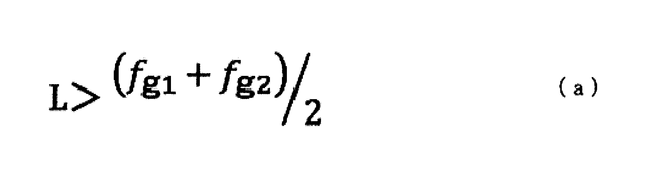
- the light guide unit 200 forms a Kepler type optical system that once focuses between the lens group 220 and the lens group 250 (see FIG. 2). Accordingly, the distance L between the lens group 220 and the lens group 250 is required to be larger than the sum of the focal length fg 1 of the lens group 220 and the focal length fg 2 of the lens group 250.
- the subject-side transparent body 210 has negative power.
- the image by the lens group 220 is formed at a position that is shorter than the focal length fg 1 .
- the focal length fg 2 of the lens group 250 is limited by the plane size of the pixel 10
- the focal length fg 1 of the lens group 220 is not subject to such limitation, and is assumed to be long. Is done. Therefore, in the present embodiment, in consideration of the above, the focal length fg 1 of the lens group 220 so as to form a Keplerian optical system that once focuses between the lens group 220 and the lens group 250. It is preferable that the focal length fg 2 of the lens group 250 and the distance L between the lens group 220 and the lens group 250 satisfy the following conditional expression (a).
- the light-shielding part 240 which shields the light which has the opening part 240a which overlaps with the focus located between the lens group 220 and the lens group 250 is provided.
- the angle range of incident light incident on the pixel 10 positioned at the center of the imaging element surface (image plane) is derived so as to satisfy the following conditional expression (b). It is preferable to configure the optical unit 200.
- the range of the angle ⁇ formed by the upper ray and the lower ray incident on the pixel 10 located at the center of the imaging element surface is expressed by the following conditional expression (b) Is preferably satisfied.
- conditional expression (b) the condensing direction is a negative value, and the divergence direction is a positive value.
- each pixel 10 is required to be adjusted to have a predetermined angle of view that does not overlap with the adjacent pixel 10. And in order to avoid the above duplication, it is preferable that angle (theta) which an upper ray and a lower ray make is 10 degrees or less, for example.
- the subject is used in close proximity to the solid-state imaging device 1.
- the angle ⁇ formed by the upper light beam and the lower light beam is a condensing direction, that is, a negative value.
- a cover glass 400 see FIG. 3
- a protective film is provided to protect the light guide unit 200. Therefore, the length of the light guide unit 200 may be shorter than the distance from the subject to the light guide unit 200.
- the range of the angle ⁇ formed by the upper ray and the lower ray incident on the pixel 10 located at the center of the image sensor surface is more preferably ⁇ 2 ° ⁇ ⁇ ⁇ 2 °.
- the focal length fg 2 of the lens group 250 satisfies the following conditional expression (c).
- the plurality of pixels 10 are assumed to have a size of several mm or less and about 0.6 ⁇ m or more. Therefore, it is assumed that the focal length fg 2 of the lens group 250 is larger than 0.0005 mm because it is limited by the size of the pixel 10. Further, in the solid-state imaging device 1 according to the present embodiment, the length of the light guide unit 200 is assumed to be 3 mm or less considering that the light guide unit 200 is included in the pixel 10. Therefore, in the present embodiment, the focal length fg 2 of the lens group 250 is required to be less than 3 mm.
- the focal length fg 2 of the lens group 250 is more preferably 1 mm> fg 2 > 0.0003 mm.
- the operation of the light guide unit 200 according to the present embodiment that is, how light travels in the light guide unit 200 will be described with reference to FIG.
- the illustration of the light shielding portion 240 is omitted for the sake of clarity.
- FIG. 2 shows two incident lights 600a and 600b. Specifically, as the incident light 600 a, an upper ray and a lower ray centered on the principal ray are illustrated along with a principal ray perpendicular to the imaging element surface of the solid-state imaging device 300. Further, as the incident light 600b, an upper ray and a lower ray centered on the principal ray are shown together with a principal ray inclined about 5 degrees with respect to the principal ray of the incident light 600a. Note that the lower light beam of the incident light 600b protrudes from the light guide unit 200, and therefore should be detected by the adjacent solid-state imaging device 300, in other words, incident light to be shielded.
- the incident light 600 a and the incident light 600 b are formed at the imaging position 500.
- the imaging position 500 the imaging of the incident light 600a and the imaging of the incident light 600b can be separated by about 2.3 ⁇ m.
- the image formation of the incident light 600a and the image formation of the incident light 600b are separated by only about 0.6 ⁇ m.
- the image of the incident light 600a and the image of the incident light 600b are very close to each other, and the incident light 600a and the incident light 600b overlap each other. Therefore, if the incident light 600b is to be shielded on the image sensor surface 502, at least a part of the incident light 600a that should be detected by the solid-state image sensor 300 may be shielded. In such a case, the incident light 600a may be shielded. The use efficiency will be reduced. Although it is conceivable to block the incident light 600b on the subject side (left side of the pixel 10), since the incident light 600a and the incident light 600b overlap each other also on the subject side, at least one of the incident light 600a. There is a risk of shading the part.
- the imaging of the incident light 600a and the imaging of the incident light 600b are sufficiently separated. Therefore, by providing the light shielding portion 240 at the imaging position 500, the incident light 600b can be shielded without shielding the incident light 600a that should be detected by the solid-state imaging device 300. That is, according to the present embodiment, in the solid-state imaging device 1 that uses a microlens having a plane size of the same level as the unit pixel of the solid-state imaging device without using the imaging lens, overlapping of the angle of view of the adjacent pixels 10 is avoided. However, the utilization efficiency of the incident light 600a can be improved.
- the light guide unit 200 includes a transparent body 210.
- the transparent body 210 is, for example, a transparent body having a d-line refractive index of 1.55 and a length of 50 ⁇ m.
- the lens group 220 includes a microlens (first microlens) 222 having a convex shape toward the solid-state imaging device 300 side and a microlens (second microlens) having a convex shape toward the subject side. , And a transparent body (fourth transparent body) 224 provided with the microlens 222 and the microlens 226 therebetween.
- the microlens 222 is, for example, a lens material having a d-line refractive index of 1.9 and a thickness of 5 ⁇ m, and the curvature of the lens is ⁇ 15 ⁇ m.
- the microlens 226 is, for example, a 1 ⁇ m-thick lens material having a d-line refractive index of 1.9, and the lens curvature is 15 ⁇ m.
- the transparent body 224 is, for example, a 3 ⁇ m thick transparent body having a d-line refractive index of 1.48. Note that the microlenses 222 and 226 may be realized by a diffraction element or the like.
- the light guide unit 200 includes a transparent body (second transparent body) 230 between the lens group 220 and the lens group 250.
- the transparent body 230 is a transparent body having a d-line refractive index of 1.55 and a length of 70 ⁇ m, for example.
- the transparent body 230 is provided with the above-described light shielding portion 240.
- the light shielding part 240 is an opening light shielding body having an opening 240a in the center as described above.
- the lens group 250 includes a microlens (fourth microlens) 252 having a convex shape toward the solid-state imaging device 300 side and a microlens having a convex shape toward the object side (fourth microlens).
- the microlens 252 is, for example, a 1 ⁇ m-thick lens material having a d-line refractive index of 1.9, and the lens curvature is ⁇ 7 ⁇ m.
- the microlens 256 is, for example, a 1 ⁇ m-thick lens material having a d-line refractive index of 1.9, and the lens curvature is 7 ⁇ m.
- the transparent body 254 is a 2 ⁇ m-thick transparent body having a d-line refractive index of 1.48, for example. Note that the microlenses 252 and 256 may be realized by a diffraction element or the like.
- the light guide unit 200 further includes a transparent body (third transparent body) 260 between the lens group 250 and the solid-state imaging device 300.
- the transparent body 260 is, for example, a transparent body having a d-line refractive index of 1.55 and a length of 17 ⁇ m.
- lens material and the transparent body described above can be formed of SiO2, SiN, glass, or the like.
- the light guide unit 200 is preferably filled with a transparent medium other than air from the transparent body 210 on the subject side to the solid-state imaging device 300.
- FIG. 3 Details of the solid-state imaging device 1 configured by arranging a plurality of such pixels 10 will be described with reference to FIGS.
- a plurality of pixels 10 are arranged, and a cover glass 400 is provided on the subject side of the plurality of pixels 10.
- the cover glass 400 is provided on the subject-side surface of the transparent body 210 in common with the plurality of pixels 10.
- the cover glass 400 is made of a glass material having a d-line refractive index of 1.55 and a thickness of 45 ⁇ m, for example.
- the transparent body 210 mentioned above consists of two transparent bodies 210b and 210c.
- the transparent body 210b is, for example, a transparent body having a d-line refractive index of 1.55 and a thickness of 5 ⁇ m
- the transparent body 210c has a role of refracting a principal ray of 5 ⁇ m with a d-line refractive index of 1.9. It is a transparent body.
- the other elements of the light guide unit 200 are the same as those of the light guide unit 200 of FIG. 1 described above, and thus the description thereof is omitted here.
- each pixel 10 is arranged in the vertical direction, and in each pixel 10, the optical axis passing through the center of the field angle is the angle of view of the pixel 10 located at the center of the image sensor surface 502.
- the optical axis passing through the center is perpendicular to the image pickup element surface
- the solid-state imaging device 1 by tilting as described above, it is possible to configure the solid-state imaging device 1 having a desired angle of view for the plurality of pixels 10 as a whole.
- the length of one side of the imaging element surface 502 on which the plurality of solid-state imaging elements 300 are arranged is about 152.2 ⁇ m.
- the surface of the transparent body 210c that refracts the principal ray is -41 °, -41 °, -41 °, -34.
- Each transparent body 210c is inclined so that 5 °, ⁇ 25.5 °, ⁇ 12.75 °, 0 °, 12.75 °, 25.5 °, 34.5 °, 41, 41 °, and 41 ° are inclined. It is preferable to be provided.
- incident light is decentered upward by 4.8 ⁇ m by the microlens 222 of the lens group 220 of the uppermost pixel 10 in FIG. 3, and the lens of the second pixel 10 from the upper side in FIG.
- Incident light is decentered upward by 2.4 ⁇ m by the micro lens 222 of the group 220.
- the incident light is decentered 2.4 ⁇ m downward by the micro lens 222 of the lens group 220 of the second pixel 10 from the bottom in FIG. 3, and the micro lens 222 of the lens group 220 of the bottom pixel 10 in FIG.
- Incident light is decentered 8 ⁇ m downward.
- the solid-state imaging device 1 having a desired angle of view can be configured with the plurality of pixels 10 as a whole. That is, the solid-state imaging device 1 according to the present embodiment can function as an imaging device (camera) having a predetermined angle of view even without an imaging lens (objective lens).
- each transparent body 210c is provided such that the subject-side surface of the transparent body 210c has a different angle with respect to the image sensor surface 502 for each pixel 10.
- each microlens 222 has a surface on the solid-state imaging device 300 side of the microlens 222 that has a different angle with respect to the imaging device surface 502 for each pixel 10. It is provided as follows. Specifically, in this embodiment, for each position of the pixel 10, the object-side surface of the transparent body 210 c and the surface of the microlens 222 on the solid-state imaging device 300 side are sequentially inclined to refract incident light.
- the incident light is refracted on differently inclined surfaces, so that the angles of chief rays are different from one another for each pixel 10, and the solid-state imaging device 1 having a desired angle of view is configured for the plurality of pixels 10 as a whole. be able to.
- the surface of the transparent body 210c and the microlens 222 has a different angle with respect to the imaging element surface 502 for each predetermined number of pixels 10 instead of for each pixel 10. May be provided.
- incident light may not be refracted depending on the angle of the surface, but may be refracted using, for example, a difference in refractive index between the transparent bodies 210b and 210c.
- the incident light forms an image once between the lens group 220 and the lens group 250 and forms an image again on the image sensor surface 502 of the solid-state image sensor 300.
- one pixel 10 has an optical axis perpendicular to the imaging element surface 502 of the solid-state imaging element 300 included in the pixel 10 between at least the surface of the lens group 250 on the solid-state imaging element 300 side and the solid-state imaging element 300. Have in.
- FIG. 4 shows the solid-state imaging device 1 in which 13 pixels 10 are arranged in the vertical direction and the horizontal direction.
- the number and arrangement of the pixels 10 are shown in FIG. It is not limited to the form shown and can be selected as appropriate.
- the pixel 10 has been described as having one solid-state imaging device 300 and one light guide unit 200. However, in the present embodiment, the present invention is not limited to this.
- the pixel 10 may include a plurality of solid-state imaging devices 300 and a light guide unit 200. In this case, the plurality of solid-state imaging devices 300 in one pixel 10 have a common principal ray.
- the adjacent pixels 10 can be further increased while avoiding overlapping of the angle of view.
- an imaging lens object lens
- it is difficult to use a general imaging lens and it is possible to manufacture a solid-state imaging device that detects infrared light at low cost. It becomes.
- the solid-state imaging device 1 having no chromatic aberration can be provided.
- this embodiment is applied to the solid-state imaging device 1 that simultaneously detects infrared light and visible light, it is possible to suppress the occurrence of a focus difference between infrared light and visible light.
- the solid-state imaging device 1 according to this embodiment described above does not have an imaging lens, it can be manufactured by a semiconductor manufacturing process. As a result, according to this embodiment, an increase in manufacturing cost can be suppressed.
- FIG. 5 is a schematic diagram of a cross section of the solid-state imaging device 1a according to the present embodiment.
- the lens groups 220 and 250 and two microlenses 222, 226, 252, and 256 are included, respectively.
- one microlens 222a and 256a is included, respectively.
- the micro lens 222a corresponds to the micro lens 222 of the lens group 220 according to the first embodiment
- the micro lens 256a corresponds to the micro lens 256 of the lens group 250 according to the first embodiment.
- the light guide unit 200a is common between the microlens 222a and the microlens 256a, as in the first embodiment, in common with the first embodiment.
- the micro lenses 222a and 256a may be realized by a diffractive element or the like, as in the first embodiment.
- FIG. 6 is a schematic cross-sectional view of the solid-state imaging device 1b according to this embodiment.
- the light guide 200 is protected using the cover glass 400.
- the cover glass 400 may not be provided, the incident light is directly incident on the light guide unit 200 from the air, and the incident light is refracted by the transparent body 210 or the like. You may let them.
- the points other than those described above are the same as those in the first embodiment, and the light guide unit 200 is focused between the lens group 220 and the lens group 250 as in the first embodiment. It becomes a Kepler type optical system.
- action of the light guide part 200 in this embodiment is the same as that of 1st Embodiment, detailed description is abbreviate
- FIG. 7A is a schematic cross-sectional view of the solid-state imaging device 1c according to the present embodiment.
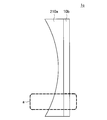
- 7B is an enlarged view of a region a in FIG. 7A
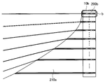
- FIG. 7C is an enlarged view of a region b in FIG. 7B.
- the solid-state imaging device 1b has a plurality of transparent bodies 210 that serve to refract chief rays incident directly from air.
- the solid-state imaging device 1c has one lens having a continuous concave surface, in which a plurality of transparent bodies 210 are integrated.
- a lens having a concave surface is provided as the transparent body 210a common to the plurality of pixels 10c.
- FIG. 7B which is an enlarged view of the region a in FIG. 7A, a plurality of pixels 10b are arranged, and the transparent body 210a common to the plurality of pixels 10b receives the chief ray of each pixel 10b.
- a concave surface is provided on the object side so as to be sequentially refracted.
- the transparent body 210a is a transparent body having a curvature radius of 4.1 mm.
- the solid-state imaging device 1c is arranged on a plane having a maximum radius of 2 mm within a range of 2.4 mm ⁇ 3.2 mm in length and width. 400 ⁇ 533 solid-state imaging devices 300 are arranged. Furthermore, each pixel 10b has a light guide portion 200b as shown in FIG. 7C, which is an enlarged view of the region b in FIG. 7B. In the fourth embodiment, the points other than those described above are the same as those in the first embodiment, and the light guide unit 200b is focused between the lens group 220 and the lens group 250, as in the first embodiment. It becomes a Kepler type optical system.
- the solid-state imaging device 1 according to each embodiment of the present disclosure described above can be applied to electronic devices such as a fingerprint authentication device 700, a face / iris authentication device 710, and a research observation device.
- An application example of the solid-state imaging device 1 according to the present embodiment will be described with reference to FIGS. 8 to 10.
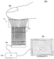
- FIG. 8 is a schematic diagram of a fingerprint authentication apparatus 700 according to this embodiment
- FIG. 9 is a schematic diagram of a face authentication apparatus 710 according to this embodiment.
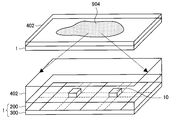
- FIG. 10 is an explanatory diagram for explaining a method of using the solid-state imaging device 1 according to the present embodiment, and in detail, an explanation explaining a case where the solid-state imaging device 1 is applied to a research observation apparatus.
- FIG. 8 is a schematic diagram of a fingerprint authentication apparatus 700 according to this embodiment
- FIG. 9 is a schematic diagram of a face authentication apparatus 710 according to this embodiment
- FIG. 10 is an explanatory diagram for explaining a method of using the solid-state imaging device 1 according to the
- the fingerprint authentication device 700 is a device that performs fingerprint authentication, and includes the solid-state imaging device 1 according to the present embodiment as a fingerprint sensor unit that detects a fingerprint. Furthermore, the fingerprint authentication device 700 includes a processing unit 702 and a display unit 704.
- the processing unit 702 is a device that authenticates a fingerprint detected by the solid-state imaging device 1 and is realized by, for example, a personal computer.
- the display unit 704 is a device that displays a fingerprint or an authentication result detected by the solid-state imaging device 1. For example, a CRT (Cathode Ray Tube) display device, a liquid crystal display (LCD) device, an OLED (Organic Light Emitting Diode). ) Realized by a device or the like.
- CTR Cathode Ray Tube
- LCD liquid crystal display
- OLED Organic Light Emitting Diode
- the solid-state imaging device 1 images the fingerprint of the finger 900 according to control from the processing unit 702 and transmits image data to the processing unit 702 via the signal line 706. Then, the processing unit 702 compares the received image data with registration information, which is a fingerprint image registered in the processing unit 702 in advance, and determines the success or failure of the authentication. Then, the processing unit 702 outputs an authentication result and a captured fingerprint image to the display unit 704.
- the fingerprint authentication apparatus 700 can be an apparatus that authenticates a user's veins as well as fingerprint authentication.
- the face authentication device 710 is a device that performs face authentication, and includes the solid-state imaging device 1 according to the present embodiment as an imaging unit that images a face. Further, the face authentication device 710 includes a processing unit 702 and a display unit 704, similarly to the above-described fingerprint authentication device 700.
- the processing unit 702 is a device that performs authentication on the face image captured by the solid-state imaging device 1, and is realized by, for example, a personal computer.
- the display unit 704 is a device that displays a face image captured by the solid-state imaging device 1 and an authentication result, and is realized by, for example, a CRT display device.
- the operation of the face authentication device 710 is substantially the same as that of the above-described fingerprint authentication device 700, and thus detailed description thereof is omitted here.
- the face authentication apparatus 700 can be an apparatus that authenticates not only a face but also an iris.
- the solid-state imaging device 1 can image a subject close to the solid-state imaging device 1, such as a fingerprint of a finger 900. Therefore, according to the present embodiment, for example, it is possible to provide the solid-state imaging device 1 that is an authentication device that simultaneously performs fingerprint authentication / iris authentication / vein authentication and face authentication.
- the solid-state imaging device 1 is applied to a research observation apparatus for a sample 904 such as a cell
- the solid-state imaging device 1 according to the present embodiment can be applied to an apparatus that observes a sample 904 such as a cell mounted on a cover glass 402 from a close position.
- the solid-state imaging device 1 according to the present embodiment can be disposed so as to be in contact with the cover glass 402 on which the sample 904 is mounted.
- the solid-state imaging device 1 arranged in this way can function like a microscope having no objective lens, and can observe the sample 904 in detail with a simple configuration.
- the solid-state imaging device 1 can function as a research or medical observation device such as a lensless microscope for discriminating, selecting, and separating cells and viruses.
- the cover glass 402 is not limited to a glass material, and may be a PET (Poly-Ethylene Terephthalate) resin or the like as long as it is a transparent member.
- an optical member such as a band pass filter may be provided before and after the cover glass 400 or between various microlenses.
- the solid-state imaging device 1 according to the present embodiment is not limited to being applied to the above-described fingerprint authentication device 700, face authentication device 710, and research observation device.
- the solid-state imaging device 1 according to this embodiment includes a vein authentication device for performing vein authentication, an iris authentication device for performing iris authentication, a lensless microscope for distinguishing and separating cells, viruses, and the like.
- the present invention can be applied to various electronic devices such as research or medical observation devices, various inspection devices used for inspection of semiconductor devices and glass, and contact-type copying machines.
- FIG. 12A is a schematic cross-sectional view of the solid-state imaging device 1d according to the present embodiment.
- FIG. 12B is an enlarged view of a region c in FIG. 12A.
- a biconcave lens 404 (a lens whose both surfaces are concave) is used instead of the cover glass 400.
- the pixel 10b is arranged with a space (a space filled with air) separated from the biconcave lens 404.
- the pixel 10 b includes a light guide unit 200 c that does not have a transparent body 210 and a solid-state imaging device 300.
- a plurality of pixels 10d are arranged, and a biconcave lens 404 is provided on the subject side of the plurality of pixels 10b.
- the biconcave lens 404 is a lens having negative power.
- precise alignment is unnecessary, and light is effectively condensed on the pixel 10b without significantly bending the light. be able to.
- the biconcave lens 404 is a lens having a spherical surface with a radius of curvature of ⁇ 9 mm, a center thickness of the lens of 0.33 mm, and a radius of curvature of 3.47 mm, and is a plastic biconcave lens equivalent to ZEONEX z300r of ZEON Corporation. be able to.
- the biconcave lens 404 may be a diffraction grating instead of a lens having negative power.
- the pixel 10b is arranged at a distance of 0.71 mm from the pixel side center of the biconcave lens 404.
- the optical axis passing through the center of the angle of view is an image of the pixel 10b located at the center of the image sensor surface 502.
- the optical axis passing through the center of the corner in the order from the top in FIG. 12B, ⁇ 29.5 °, ⁇ 22.5 °, ⁇ 17.1 °, ⁇ 12.3 °, -7.9 °, -3.9 °, 0 °, 3.9 °, 7.9 °, 12.3 °, 17.1 °, 22.5 °, 29.5 ° It is like that.
- the solid-state imaging device 1d by tilting as described above, it is possible to configure the solid-state imaging device 1d having a desired angle of view for the plurality of pixels 10b as a whole.
- the length of one side of the imaging element surface 502 on which the plurality of solid-state imaging elements 300 are arranged is about 1.122 mm.
- the plane of the solid-state imaging device 1d according to the present embodiment is the same as the plane of the first solid-state imaging device 1 described with reference to FIG. 4, here, the solid-state imaging device 1d according to the present embodiment. The description of the plane is omitted.
- the pixel 10b will be described with reference to FIG. 1.
- the light guide unit 200c that does not have the transparent body 210 and the solid-state imaging. Device 300 is formed.
- the light guide unit 200c includes a lens group 220 having a positive optical power, a light shielding unit 240, and a lens group 250 having a positive optical power from the subject side toward the solid-state imaging device 300 side. Including.
- the lens group 220 includes a microlens 222 having a convex shape toward the solid-state imaging device 300 side, a microlens 226 having a convex shape toward the subject side, and a microlens. 222 and a transparent body 224 provided between the microlens 226.
- the microlens 222 is, for example, a lens material having a d-line refractive index of 1.9 and a thickness of 5 ⁇ m, and the curvature of the lens is ⁇ 15 ⁇ m.
- the microlens 226 is, for example, a 1 ⁇ m-thick lens material having a d-line refractive index of 1.9, and the lens curvature is 15 ⁇ m.
- the transparent body 224 is, for example, a 3 ⁇ m thick transparent body having a d-line refractive index of 1.48. Note that the microlenses 222 and 226 may be realized by a diffraction element or the like.
- the light guide unit 200 c includes a transparent body 230 between the lens group 220 and the lens group 250.
- the transparent body 230 is, for example, a transparent body having a d-line refractive index of 1.55 and a length of 50 ⁇ m.
- the transparent body 230 is provided with the above-described light shielding portion 240.
- the light shielding part 240 is an opening light shielding body having an opening 240a in the center as described above.
- the lens group 250 includes a microlens 252 having a convex shape toward the solid-state imaging device 300 side, a microlens 256 having a convex shape toward the subject side, and the microlens 252 and the microlens 256.
- the microlens 252 is, for example, a 1 ⁇ m-thick lens material having a d-line refractive index of 1.9, and the curvature of the lens is ⁇ 6 ⁇ m.
- the microlens 256 is, for example, a 1 ⁇ m-thick lens material having a d-line refractive index of 1.9, and the lens curvature is 6 ⁇ m.
- the transparent body 254 is a 2 ⁇ m-thick transparent body having a d-line refractive index of 1.48, for example. Note that the microlenses 252 and 256 may be realized by a diffraction element or the like.
- the light guide unit 200 c further includes a transparent body 260 between the lens group 250 and the solid-state imaging device 300.
- the transparent body 260 is, for example, a transparent body having a d-line refractive index of 1.55 and a length of 20.1 ⁇ m.
- the use of the biconcave lens 404 having such a negative power eliminates the need for precise alignment and effectively eliminates the light from being bent greatly. It is possible to collect light.
- a solid-state imaging device 1d according to a seventh embodiment of the present disclosure which is a modification of the biconcave lens 404, will be described with reference to FIGS. 12A and 12B.
- a biconcave lens 404 different from that in the sixth embodiment is used, but the pixel 10b is common to the sixth embodiment.
- a plurality of pixels 10d are arranged, and a biconcave lens 404 is provided on the subject side of the plurality of pixels 10b.
- the biconcave lens 404 is a lens having negative power. Also in the present embodiment, by using the biconcave lens 404 having such a negative power, precise alignment is unnecessary, and light is effectively condensed on the pixel 10b without significantly bending the light. Can do.
- the biconcave lens 404 is a lens having a spherical surface with a radius of curvature of ⁇ 13.2 mm, a center thickness of the lens of 0.33 mm, and a radius of curvature of 5 mm. it can.
- the pixel 10b is arranged at a distance of 0.5 mm from the center of the biconcave lens 404 on the pixel side.
- the optical axis passing through the center of the angle of view is an image of the pixel 10b located at the center of the image sensor surface 502.
- the optical axis passing through the center of the corner in the order from the top in FIG. 12B, ⁇ 38.3 °, ⁇ 29.5 °, ⁇ 22.8 °, ⁇ 16.7 °, -10.8 °, -5.3 °, 0 °, 5.3 °, 10.8 °, 16.7 °, 22.8 °, 29.8 °, 38.3 ° It is like that.
- the solid-state imaging device 1d by tilting as described above, it is possible to configure the solid-state imaging device 1d having a desired angle of view for the plurality of pixels 10b as a whole.
- the length of one side of the imaging element surface 502 on which the plurality of solid-state imaging elements 300 are arranged is about 0.912 mm.
- the plane of the solid-state imaging device 1d according to the present embodiment is the same as the plane of the first solid-state imaging device 1 described with reference to FIG. The description of the plane is omitted.
- the use of the biconcave lens 404 having such a negative power eliminates the need for precise alignment and effectively eliminates the light from being bent greatly. It is possible to collect light.
- the lens having negative power on the subject side is not limited to being realized by one lens, and may be realized by two or more lenses, and is particularly limited. It is not a thing.
- FIG. 13 is a schematic diagram of a pixel 10c according to the present embodiment.
- the lens groups 220 and 250 of the light guide unit 200 are realized by two microlenses, but the light guide unit 200d of the pixel 10c of the present embodiment.
- a single microlens 228 and 258 may be used instead of the lens groups 220 and 250.
- one of the lens groups 220 and 250 of the light guide unit 200 may be realized by two microlenses, and the other may be realized by one microlens. It may be realized with a microlens and is not particularly limited.
- FIG. 14 is a schematic diagram of the fingerprint authentication device 700a according to the present embodiment
- the solid-state imaging device 1e using the pixel 10c can be applied to the fingerprint authentication device 700a.
- the cover glass 400 is illustrated as being present between the solid-state imaging device 1e and the finger 900, but in the present embodiment, the configuration example illustrated in FIG. It is not limited.
- the lens biconcave lens 404 having negative power on the object side in the sixth and seventh embodiments described above may be used. It may be configured to directly contact the finger 900 without going through the lens 400 or the lens having negative power on the subject side.
- the following effects can be obtained by using the solid-state imaging device 1 or the electronic apparatus according to the embodiment of the present disclosure. Needless to say, the effects produced by using the solid-state imaging device 1 or the electronic apparatus according to the present embodiment are not limited to the examples shown below.
- incident light is used in a solid-state imaging device that uses a microlens having a planar size of the same level as a unit pixel of a solid-state imaging device and having a total length of 1 mm or less without using an imaging lens (objective lens). Can be used more efficiently.
- an imaging lens since an imaging lens is not used, a solid-state imaging device having no chromatic aberration can be provided.
- a solid-state imaging device can be manufactured by a semiconductor manufacturing process, it is possible to manufacture a solid-state imaging device and an electronic apparatus including the solid-state imaging device with reduced manufacturing costs.
- (5) it is possible to image a subject close to the subject, and thus it is possible to image a subject on a cover glass of a solid-state imaging device or a cover glass provided in proximity to the solid-state imaging device. It is. Therefore, according to the embodiment of the present disclosure, for example, it is possible to provide a solid-state imaging device of an authentication device that performs fingerprint authentication / iris authentication / vein authentication and face authentication at the same time.
- a lensless microscope that can be used for cell selection, virus discrimination, and the like.
- the above-described solid-state imaging device 300 can be a CCD (image sensor or CMOS image sensor).
- Each pixel is At least one solid-state imaging device; At least one light guide provided on the subject side of the solid-state imaging device; Have The light guide unit is directed from the subject side toward the solid-state image sensor side along the light guide direction of the light guide unit.
- the light guide is a Keplerian optical system that focuses between the first lens group and the second lens group; The opening of the light shielding portion is provided so as to overlap the focal point;
- the focal length fg 1 of the first lens group, the focal length fg 2 of the second lens group, and the distance L between the first lens group and the second lens group satisfy the following conditions:
- the range of the angle ⁇ formed by the upper ray and the lower ray incident on the pixel located at the center of the imaging element surface satisfies the following conditional expression (b), and is a solid-state imaging device according to (3) above.
- the conditional expression (b) the light collection direction is a negative value, and the divergence direction is a positive value.
- the solid-state imaging device includes a first microlens having a convex shape toward the solid-state image sensor side.
- the solid-state imaging device according to any one of (1) to (5) above.
- the solid-state imaging device according to (6), wherein a surface of the first microlens on the solid-state imaging device side has a different angle with respect to the imaging device surface for each pixel.
- the first lens group is directed from the subject side toward the solid-state image sensor side along the light guide direction of the light guide unit.
- the first lens group includes: A fourth transparent body provided between the first microlens and the second microlens; The solid-state imaging device according to (8) above.
- the solid-state imaging device according to (10), wherein the plurality of first transparent bodies are integral lenses.
- the solid-state imaging device (13) The solid-state imaging device according to (1), wherein the first transparent body is a lens having negative optical power. (14) The said lens is a solid-state imaging device as described in said (13) which is a biconcave lens whose both surfaces are concave. (15) The solid-state imaging device according to (14), wherein a space filled with air exists between the lens and the first lens group. (16) The second lens group includes a third microlens having a convex shape toward the subject side. The solid-state imaging device according to any one of (1) to (12) above.
- the second lens group from the subject side toward the solid-state imaging device side along the light guide direction of the light guide unit, A fourth microlens having a convex shape toward the solid-state image sensor side; The third microlens; Sequentially The solid-state imaging device according to (16) above.
- the second lens group includes: A fifth transparent body provided between the fourth microlens and the third microlens; The solid-state imaging device according to (17) above.
- An electronic apparatus including a solid-state imaging device having a plurality of pixels arranged in a matrix on an imaging element surface, Each pixel is At least one solid-state imaging device; At least one light guide provided on the subject side of the solid-state imaging device; Have The light guide unit is directed from the subject side toward the solid-state image sensor side along the light guide direction of the light guide unit.
- Solid-state imaging device 10 10a, 10b, 10c, 20 pixels 200, 200a, 200b, 200c, 202
Landscapes
- Physics & Mathematics (AREA)
- Engineering & Computer Science (AREA)
- Multimedia (AREA)
- Signal Processing (AREA)
- General Physics & Mathematics (AREA)
- Optics & Photonics (AREA)
- Solid State Image Pick-Up Elements (AREA)
- Transforming Light Signals Into Electric Signals (AREA)
Abstract
【課題】近接する固体撮像素子間での入射光の重複を避けつつ、入射光の利用効率を高めることが可能な固体撮像装置及び電子機器を提供する。 【解決手段】撮像素子面上にマトリックス状に配置された複数の画素を備え、前記各画素は、少なくとも1つの固体撮像素子と、前記固体撮像素子の被写体側に設けられた少なくとも1つの導光部と、を有し、前記導光部は、当該導光部の導光方向に沿って前記被写体側から前記固体撮像素子側に向かって、第1の透明体と、正の光学的パワーを持つ第1のレンズ群と、開口部を持つ遮光部と、正の光学的パワーを持つ第2のレンズ群と、を順次含む、固体撮像装置を提供する。
Description
本開示は、固体撮像装置及び電子機器に関する。
撮像レンズ(対物レンズ)の代わりに、固体撮像素子の単位画素と同レベルの平面サイズを持つ、全長が3mm以下のマイクロレンズを用いる固体撮像装置としては、例えば、下記特許文献1及び2に開示された装置を挙げることができる。ところで、上述のような固体撮像装置においては、1つの撮像素子平面に複数の固体撮像素子がマトリックス状に近接して配置されている。当該固体撮像装置は、上述の複数の固体撮像素子のそれぞれが取得した撮像情報を1つに合成することにより被写体の像を得ることができる。従って、当該固体撮像装置においては、各固体撮像素子が互いに重複することなく、所定の範囲からの入射光を検出し、検出した入射光に係る撮像情報を得ることが求められることから、各固体撮像素子を含む各画素は、互いに重複しない狭い画角を持つことが好ましい。
そこで、上述のような重複を避けるため、下記特許文献1においては、マイクロレンズと固体撮像素子との間に2つのピンホールを設けており、また、下記特許文献2においては、1つのピンホールを設けている。下記特許文献1及び2においては、上記ピンホールにより各固体撮像素子が検出することができる入射光の範囲を制限することにより、各画素の画角が互いに重複することを避けている。
しかしながら、上記特許文献1及び2に開示の固体撮像装置においては、ピンホールによって、各固体撮像素子が検出することができる入射光の範囲を制限していることから、入射光の利用効率が低いといえる。
そこで、本開示では、近接する画素の画角の重複を避けつつ、入射光の利用効率を高めることが可能な、新規且つ改良された固体撮像装置及び電子機器を提案する。
本開示によれば、撮像素子面上にマトリックス状に配置された複数の画素を備え、前記各画素は、少なくとも1つの固体撮像素子と、前記固体撮像素子の被写体側に設けられた少なくとも1つの導光部とを有し、前記導光部は、当該導光部の導光方向に沿って前記被写体側から前記固体撮像素子側に向かって、第1の透明体と、正の光学的パワーを持つ第1のレンズ群と、開口部を持つ遮光部と、正の光学的パワーを持つ第2のレンズ群と、を順次含む、固体撮像装置が提供される。
さらに、本開示によれば、撮像素子面上にマトリックス状に配置された複数の画素を有する固体撮像装置を備える電子機器であって、前記各画素は、少なくとも1つの固体撮像素子と、前記固体撮像素子の被写体側に設けられた少なくとも1つの導光部とを有し、前記導光部は、当該導光部の導光方向に沿って前記被写体側から前記固体撮像素子側に向かって、第1の透明体と、正の光学的パワーを持つ第1のレンズ群と、開口部を持つ遮光部と、正の光学的パワーを持つ第2のレンズ群とを順次含む、電子機器が提供される。
以上説明したように本開示によれば、近接する画素の画角の重複を避けつつ、入射光の利用効率を高めることができる。
なお、上記の効果は必ずしも限定的なものではなく、上記の効果とともに、または上記の効果に代えて、本明細書に示されたいずれかの効果、または本明細書から把握され得る他の効果が奏されてもよい。
以下に添付図面を参照しながら、本開示の好適な実施の形態について詳細に説明する。なお、本明細書及び図面において、実質的に同一の機能構成を有する構成要素については、同一の符号を付することにより重複説明を省略する。
また、本明細書及び図面において、実質的に同一又は類似の機能構成を有する複数の構成要素を、同一の符号の後に異なる数字を付して区別する場合がある。ただし、実質的に同一又は類似の機能構成を有する複数の構成要素の各々を特に区別する必要がない場合、同一符号のみを付する。また、異なる実施形態の類似する構成要素については、同一の符号の後に異なるアルファベットを付して区別する場合がある。ただし、類似する構成要素の各々を特に区別する必要がない場合、同一符号のみを付する。
また、以下の説明で参照される図面は、本開示の一実施形態の説明とその理解を促すための図面であり、わかりやすくするために、図中に示される形状や寸法、比などは実際と異なる場合がある。さらに、図中に示される各要素は、以下の説明と公知の技術を参酌して適宜、設計変更することができる。
なお、以下の説明において、レンズについて用いられる「正のパワー」及び「負のパワー」とは、レンズによって光線を曲げる強さのことを意味し、例えば、レンズの屈折率や曲率を調整することにより、上記パワーは変化する。また、以下の説明において、レンズのパワーのうち「正のパワー」とは、光を集光する方向(レンズの内側)に曲げる強さを意味し、一方、「負のパワー」とは、光を発散する方向(レンズの外側)に曲げる強さを意味する。
また、以下の説明において、主光線とは、光学系(後述する画素10)の中心を通過する入射光を意味する。さらに、上光線とは、上記光学系の中心軸よりも上側に位置する縁を通過し、固体撮像素子で結像する入射光を意味し、下光線とは、上記光学系の中心軸よりも下側に位置する縁を通過し、固体撮像素子で結像する入射光を意味する。
また、以下の説明において、「画角」とは、各画素10が検出する画像の範囲(角度)のことを意味する。
なお、説明は以下の順序で行うものとする。
1.本発明者が本開示に係る実施形態を創作するに至った背景
2.第1の実施形態
3.第2の実施形態
4.第3の実施形態
5.第4の実施形態
6.第5の実施形態
7.第6の実施形態
8.第7の実施形態
9.第8の実施形態
10.まとめ
11.補足
1.本発明者が本開示に係る実施形態を創作するに至った背景
2.第1の実施形態
3.第2の実施形態
4.第3の実施形態
5.第4の実施形態
6.第5の実施形態
7.第6の実施形態
8.第7の実施形態
9.第8の実施形態
10.まとめ
11.補足
<<1. 本発明者が本開示に係る実施形態を創作するに至った背景>>
次に、本開示に係る各実施形態の詳細を説明する前に、本発明者が本開示に係る実施形態を創作するに至った背景について、図11を参照して説明する。なお、図11は、比較例に係る画素20の模式図である。ここで、比較例とは、本発明者が本開示の実施形態をなす前に、検討を重ねていた固体撮像装置の構成のことを意味し、詳細には、ケプラー型光学系でない構成のことを意味する。
次に、本開示に係る各実施形態の詳細を説明する前に、本発明者が本開示に係る実施形態を創作するに至った背景について、図11を参照して説明する。なお、図11は、比較例に係る画素20の模式図である。ここで、比較例とは、本発明者が本開示の実施形態をなす前に、検討を重ねていた固体撮像装置の構成のことを意味し、詳細には、ケプラー型光学系でない構成のことを意味する。
先に説明したように、撮像レンズ(対物レンズ)の代わりに、固体撮像素子の単位画素と同レベルの平面サイズを持つマイクロレンズを用いる固体撮像装置としては、例えば、上記特許文献1及び2に開示された装置を挙げることができる。ところで、上述のような固体撮像装置においては、1つの撮像素子平面に複数の固体撮像素子がマトリックス状に近接して配置されている。当該固体撮像装置は、上述の複数の固体撮像素子のそれぞれが取得した撮像情報を1つに合成することにより被写体の像を得ることができる。従って、当該固体撮像装置においては、各固体撮像素子が互いに重複することなく、被写体側からの狭い所定の範囲からの入射光を検出し、検出した入射光に係る撮像情報を得ることが求められることから、各固体撮像素子を含む各画素は、互いに重複しない狭い画角を持つように構成される。
詳細には、比較例に係る固体撮像装置は、図11の示すような、互いに近接する複数の画素20を有するものとする。各画素20は、固体撮像素子300a、300bと、被写体側からの光を各固体撮像素子300a、300bに導く導光部202とを有するものとする。なお、図11においては、左側が被写体側となる。
図11においては、固体撮像素子300aは、実線で示される入射光600a(主光線と、主光線を挟む上光線及び下光線との3つの線で示されている)だけでなく、2点破線で示される入射光600b(主光線と、主光線を挟む上光線及び下光線との3つの線で示されている)も検出している。なお、入射光600bは、入射光600aの主光線に対して5度程度傾いた主光線を持つものと仮定している。
このような場合、具体的には、入射光600aは、固体撮像素子300aの導光部202からはみ出すことなく、固体撮像素子300aへ到達する。一方、入射光600bについては、その下光線が近接する固体撮像素子300bの導光部202を通過し、固体撮像素子300aへ到達する。この入射光600bの下光線は、本来、近接する固体撮像素子300bで検出すべき入射光である。このように本来近接した固体撮像素子300bが検出すべき入射光を、固体撮像素子300aが検出してしまった場合、固体撮像素子300a、300bが検出した入射光の撮像情報は、その一部が重複する。その結果、このような場合、固体撮像素子300a、300bのそれぞれが取得した撮像情報を1つに合成しても、被写体の実像とは異なる誤った像を得てしまうこととなる。従って、このようなことを避けるために、固体撮像素子300aに入射する入射光600bの下光線を遮光し、各固体撮像素子300a、300bに係る画素20が重複することのない所定の画角を持つように調整することが求められる。
そこで、上記特許文献1及び2に開示された固体撮像装置においては、ピンホールを用いることで多方向から各固体撮像素子に入射する入射光を制限し、各画素が重複することのない所定の画角を持つように調整している。しかしながら、上記特許文献1及び2に開示の固体撮像装置においては、ピンホールによって、各固体撮像素子が検出することができる入射光の範囲を制限していることから、入射光の利用効率が低い。
そこで、このような状況を鑑みて、本発明者は、近接する画素の画角の重複を避けつつ、入射光の利用効率を高めることができないかと鋭意検討を行った。そして、このような検討の中で、本発明者は、固体撮像素子へと光を導く導光部において、固体撮像素子で結像する前に、一度結像するケプラー型光学系を利用することを独自に着想した。
詳細には、ケプラー型光学系ではない比較例においては、本発明者の検討によれば、図11に示すように、入射光600aと入射光600bとは、固体撮像素子300aの撮像素子面502において結像する。固体撮像素子300aに入射する入射光600bの下光線を、ピンホール等を用いて遮光しようとする場合には、入射光600aと入射光600bとの重なりが少ない上記結像の箇所で遮光を行うことが好ましい。しかしながら、図11からわかるように、入射光600a及び入射光600bの結ぶ結像の位置は非常に近接していることから、撮像素子面502の近傍においても入射光600aと入射光600bとが互いに重なっている。従って、撮像素子面502において入射光600bの下光線を遮光しようとする場合には、本来固体撮像素子300aで検出すべき入射光600aの少なくとも一部を遮光してしまう恐れがある。
一方、本発明者の検討によれば、ケプラー型光学系を利用して固体撮像素子300で結像する前に、手前で一度結像させるようにした場合には、詳細は後述するが(図2 矢印参照)、手前での入射光600a、600bの結像の位置は、上述の比較例よりも離すことが可能であることが分かった。このような独自の知見を踏まえて、本発明者は、手前で結像する箇所に遮光部240(図1 参照)を設けることにより、本来固体撮像素子300aで検出すべき入射光600aを遮光することなく、入射光600bの下光線を遮光できることを独自に着想した。
すなわち、本発明者は、上述の独自の着想に基づき、ケプラー型光学系を利用することにより、近接する画素20の画角の重複を避けつつ、本来固体撮像素子300aで検出すべき入射光600aを遮光することないことから、入射光600aの利用効率を高めることができる固体撮像装置を想到したのである。言い換えると、本発明者は、撮像レンズ(対物レンズ)を用いず、固体撮像素子の単位画素と同レベルの平面サイズを持つ、全長が3mm以下のマイクロレンズを用いる固体撮像装置であって、近接する画素の画角の重複を避けつつ、入射光の利用効率を高めることができる固体撮像装置に係る実施形態を創作するに至った。以下に、本開示に係る実施形態の詳細について順次説明する。
<<2. 第1の実施形態>>
まずは、本開示の第1の実施形態に係る固体撮像装置1を図1から図4を参照して説明する。図1は、本実施形態に係る画素10の模式図であり、図2は、図1に示される導光部200における入射光の進行を図示した模式図である。また、図3は、本実施形態に係る固体撮像装置1の断面の模式図であり、図4は、本実施形態に係る固体撮像装置1の平面の模式図である。なお、図1から図3においては、図中左側が被写体側となる。
まずは、本開示の第1の実施形態に係る固体撮像装置1を図1から図4を参照して説明する。図1は、本実施形態に係る画素10の模式図であり、図2は、図1に示される導光部200における入射光の進行を図示した模式図である。また、図3は、本実施形態に係る固体撮像装置1の断面の模式図であり、図4は、本実施形態に係る固体撮像装置1の平面の模式図である。なお、図1から図3においては、図中左側が被写体側となる。
詳細には、固体撮像装置1は、被写体側からの可視光を検出して、被写体を撮像する装置である。当該固体撮像装置1の撮像素子面(像面)には、二次元格子状(マトリックス状)に複数の単位セルが配置されている。当該単位セルは、固体撮像装置1を構成する単位であり、以下の説明においては、画素10と呼び、撮像画像データにおける画素データをそれぞれ生成する。また、各画素10は、図1に示すように、少なくとも1つの固体撮像素子300と、固体撮像素子300の被写体側に設けられた少なくとも1つの導光部200とを有する。
固体撮像素子300は、例えば、CCD(Charge Coupled Device)イメージセンサ又はCMOS(Complementary Metal‐Oxide‐Semiconductor)イメージセンサであり、受光した光を光電変換してアナログの電気信号を生成するものである。生成した電気信号は、処理回路等を用いて、撮像画像データにおけるデジタルの画素データに変換される。
また、固体撮像素子300の被写体側に設けられた導光部200は、光を固体撮像素子300へ導くことができる。なお、以下の説明においては、導光部200の導光方向とは、図1中の左から右へ向かう方向、すなわち、導光部200が入射光を固体撮像素子300へ導く方向であるものとする。また、以下の説明において「長さ」とは、特段のことわりが無い限りには、導光方向に沿った長さであるものとする。
詳細には、導光部200は、図1に示すように、被写体側から固体撮像素子300側に向かって、透明体(第1の透明体)210と、正の光学的パワーを持つレンズ群(第1のレンズ群)220と、遮光部240と、正の光学的パワーを持つレンズ群(第2のレンズ群)250とを含む。本実施形態においては、導光部200は、レンズ群220とレンズ群250との間で、一度焦点を結ぶケプラー型光学系をなす(図2 参照)。従って、レンズ群220とレンズ群250との間の距離Lは、レンズ群220の焦点距離fg1及びレンズ群250の焦点距離fg2の和よりも大きいことが求められる。
さらに、被写体側の透明体210が負のパワーを持つことも想定される。そのような場合、レンズ群220による像は、焦点距離fg1よりも短い距離の位置に結ばれることとなる。加えて、レンズ群250の焦点距離fg2は、画素10の平面サイズによる制限を受けるが、レンズ群220の焦点距離fg1は、このような制限を受けることがないことから、長いことも想定される。そこで、本実施形態においては、上述のことを踏まえた上で、レンズ群220とレンズ群250との間で一度焦点を結ぶケプラー型光学系をなすように、レンズ群220の焦点距離fg1、レンズ群250の焦点距離fg2、及び、レンズ群220とレンズ群250との距離Lが、下記の条件式(a)を満足することが好ましい。
そして、本実施形態においては、図1に示すように、レンズ群220とレンズ群250との間に位置する焦点と重なる開口部240aを有する、光を遮光する遮光部240が設けられている。
また、本実施形態に係る固体撮像装置1においては、撮像素子面(像面)の中心に位置する画素10に入射する入射光の角度の範囲が以下の条件式(b)を満たすように導光部200を構成することが好ましい。詳細には、本実施形態に係る固体撮像装置1においては、撮像素子面の中心に位置する画素10に入射する上光線と下光線とがなす角度θの範囲は、下記の条件式(b)を満足することが好ましい。なお、条件式(b)においては、集光方向を負の値とし、発散方向を正の値としている。
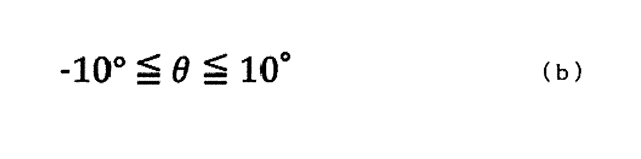
より具体的には、先に説明したように、固体撮像装置1においては、各画素10は、近接する画素10と重複することのない所定の画角を持つように調整することが求められる。そして、上述のような重複を避けるためには、上光線と下光線とがなす角度θは、例えば、10°以下であることが好ましい。
また、被写体を固体撮像装置1に近接させて使用する場合も想定される。非常に被写体を近接させた場合、上光線と下光線とがなす角度θは、集光方向、すなわち負の値となる。さらに、被写体を固体撮像装置1に近接させて使用する場合、導光部200を保護するために、カバーガラス400(図3 参照)や保護膜を設けることが想定される。従って、被写体から導光部200までの距離よりも、導光部200の長さが短くなる可能性がある。加えて、パワーが強いマイクロレンズを製造することは難しい。そこで、本実施形態においては、上述のことを踏まえた上で、カバーガラス400等を形成するガラスの光学特性を考慮すると、上光線と下光線とがなす角度θは、例えば、-10°以上であることが好ましい。
さらに、本実施形態においては、撮像素子面の中心に位置する画素10に入射する上光線と下光線とがなす角度θの範囲は、-2°≦θ≦2°であることがより好ましい。
さらに、本実施形態においては、レンズ群250の焦点距離fg2が、下記の条件式(c)を満足することが好ましい。
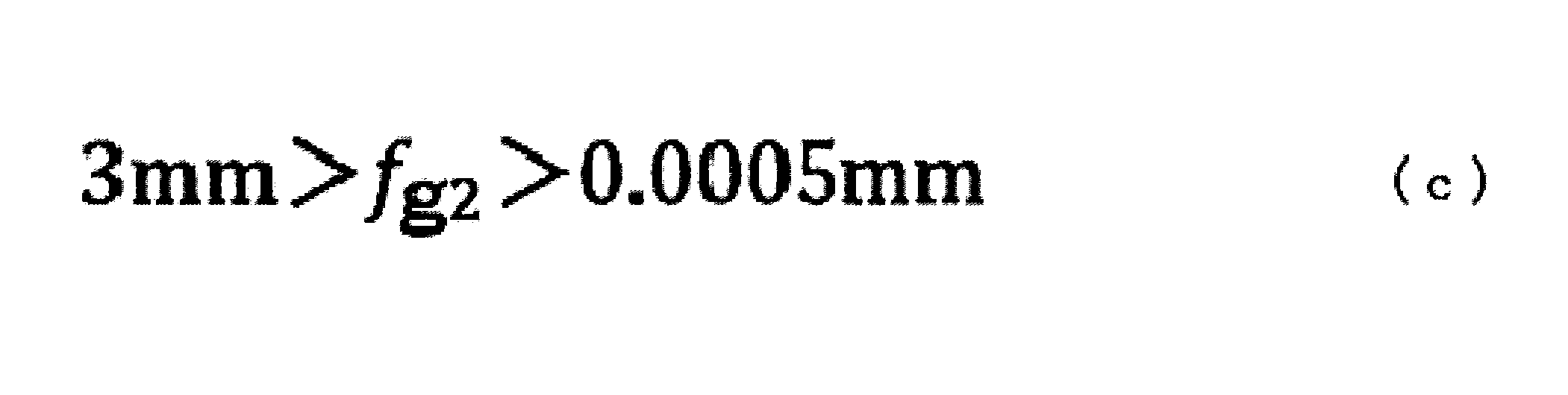
具体的には、本実施形態に係る固体撮像装置1においては、複数の画素10は、数mm以下、0.6μm程度以上のサイズであると想定される。従って、このような画素10のサイズによる制限を受けることから、レンズ群250の焦点距離fg2は、0.0005mmよりも大きくなることと想定される。また、本実施形態に係る固体撮像装置1においては、導光部200の長さは、当該導光部200が画素10に含まれることを考慮すると、3mm以下となると想定される。従って、本実施形態においては、レンズ群250の焦点距離fg2は、3mm未満であることが求められる。
さらに、本実施形態においては、レンズ群250の焦点距離fg2は、1mm>fg2>0.0003mmであることがより好ましい。
次に、このような本実施形態に係る導光部200の作用、すなわち、導光部200における光の進み方を、図2を参照して説明する。なお、図2においては、わかりやすくするために遮光部240の図示を省略している。
図2には、2つの入射光600a、600bが図示されている。詳細には、入射光600aとして、固体撮像素子300の撮像素子面に垂直な主光線とともに、当該主光線を中心とした上光線と下光線とが図示されている。また、入射光600bとして、入射光600aの主光線に対して5度程度傾いた主光線とともに、当該主光線を中心とした上光線と下光線とが図示されている。なお、入射光600bの下光線は、導光部200からはみ出ていることから、隣接する固体撮像素子300で検出されるべきであり、言い換えると、遮光すべき入射光であるものとする。
図2に示すように、本実施形態においては、レンズ群220とレンズ群250との間で一度焦点を結ぶケプラー型光学系であることから、入射光600aと入射光600bとは結像位置500において、結像する。本発明者の検討によれば、結像位置500において、入射光600aの結像と入射光600bの結像とは、2.3μm程度離すことができる。一方、図2に示すように、再度結像する撮像素子面502では、入射光600aの結像と入射光600bの結像とは、0.6μm程度しか離れていない。
詳細には、撮像素子面502においては、入射光600aの結像と入射光600bの結像とは非常に近接しており、入射光600aと入射光600bとが互いに重なっている。従って、撮像素子面502において入射光600bを遮光しようとした場合、本来固体撮像素子300で検出すべき入射光600aの少なくとも一部を遮光してしまう恐れがあり、このような場合、入射光600aの利用効率を低下させることとなる。また、被写体側(画素10の左側)で入射光600bを遮光することも考えられるが、被写体側においても、入射光600aと入射光600bとが互いに重なっていることから、入射光600aの少なくとも一部を遮光してしまう恐れがある。
一方、本実施形態においては、結像位置500においては、入射光600aの結像と入射光600bの結像とは十分に離れている。従って、結像位置500に、遮光部240を設けることにより、本来固体撮像素子300で検出すべき入射光600aを遮光することなく、入射光600bを遮光することができる。すなわち、本実施形態によれば、撮像レンズを用いず、固体撮像素子の単位画素と同レベルの平面サイズを持つマイクロレンズを用いる固体撮像装置1において、近接する画素10の画角の重複を避けつつ、入射光600aの利用効率を高めることができる。
より具体的には、図1に示すように、導光部200は、透明体210を有する。当該透明体210は、例えば、d線屈折率1.55の長さ50μmの透明体である。
レンズ群220は、図1に示すように、固体撮像素子300側に向かって凸形状を持つマイクロレンズ(第1のマイクロレンズ)222と、被写体側に向かって凸形状を持つマイクロレンズ(第2のマイクロレンズ)226と、マイクロレンズ222とマイクロレンズ226とを間に設けられた透明体(第4の透明体)224とを含む。より具体的には、マイクロレンズ222は、例えば、d線屈折率1.9の5μm厚のレンズ材であり、レンズの曲率が-15μmである。マイクロレンズ226は、例えば、d線屈折率1.9の1μm厚のレンズ材であり、レンズの曲率が15μmである。また、透明体224は、例えば、d線屈折率1.48の3μm厚の透明体である。なお、マイクロレンズ222、226は、回折素子等で実現してもよい。
また、導光部200は、レンズ群220とレンズ群250との間に、透明体(第2の透明体)230を含む。具体的には、透明体230は、例えば、d線屈折率1.55の長さ70μmの透明体である。また、透明体230には、上述の遮光部240が設けられている。当該遮光部240は、先に説明したように中央に開口部240aを持つ開口遮光体である。
さらに、レンズ群250は、図1に示すように、固体撮像素子300側に向かって凸形状を持つマイクロレンズ(第4のマイクロレンズ)252と、被写体側に向かって凸形状を持つマイクロレンズ(第3のマイクロレンズ)256と、マイクロレンズ252とマイクロレンズ256とを間に設けられた透明体(第5の透明体)254とを含む。より具体的には、マイクロレンズ252は、例えば、d線屈折率1.9の1μm厚のレンズ材であり、レンズの曲率が-7μmである。マイクロレンズ256は、例えば、d線屈折率1.9の1μm厚のレンズ材であり、レンズの曲率が7μmである。また、透明体254は、例えば、d線屈折率1.48の2μm厚の透明体である。なお、マイクロレンズ252、256は、回折素子等で実現してもよい。
さらに、導光部200は、レンズ群250と固体撮像素子300との間に、透明体(第3の透明体)260をさらに有する。具体的には、透明体260は、例えば、d線屈折率1.55の長さ17μmの透明体である。
なお、上述したレンズ材及び透明体は、SiO2、SiN、ガラス等により形成することができる。
すなわち、本実施形態においては、導光部200は、被写体側の透明体210から固体撮像素子300に至るまで、空気以外の透明な媒質で埋められていることが好ましい。
このような画素10を複数並べて構成した固体撮像装置1の詳細を図3及び図4を参照して説明する。図3に示すように、複数の画素10が並べられ、複数の画素10の被写体側の上には、カバーガラス400が設けられている。言い換えると、カバーガラス400は、複数の画素10に共通して、透明体210の被写体側の面上に設けられる。また、当該カバーガラス400は、例えば、d線屈折率1.55で45μm厚のガラス材からなる。
また、図3においては、上述した透明体210は、2つの透明体210b、210cからなる。詳細には、透明体210bは、例えば、d線屈折率1.55で5μm厚の透明体であり、透明体210cは、d線屈折率1.9で5μmの主光線を屈折させる役割を持つ透明体である。なお、導光部200の他の要素については、上述した図1の導光部200と同様であるため、ここでは説明を省略する。
図3においては、例えば縦方向に13個の画素10が並べられ、各画素10においては、画角の中心を通過する光軸が、撮像素子面502の中心に位置する画素10の画角の中心を通過する光軸(当該光軸は、撮像素子面に垂直)に対して、図中上から順に、-31.3°、-25.1°、-19.8°、-14.8°、-9.9°、-4.6°、0°、4.9°、9.9°、14.8°、19.8°、25.1°、31.3°傾くようになっている。本実施形態においては、上述のように傾けることで、複数の画素10の全体で所望の画角を有する固体撮像装置1を構成することができる。なお、例えば、複数の固体撮像素子300が並べられた撮像素子面502の1辺の長さは、約152.2μmとなる。
そこで、本実施形態においては、図3に示すように、主光線を屈折させる役割の透明体210cの表面が、図中上から順に、-41°、-41°、-41°、-34.5°、-25.5°、-12.75°、0°、12.75°、25.5°、34.5°、41、41°、41°傾けられるように、各透明体210cが設けられることが好ましい。さらに、本実施形態においては、図3中一番上の画素10のレンズ群220のマイクロレンズ222により、4.8μm上方に入射光を偏心させ、図3中上から2番目の画素10のレンズ群220のマイクロレンズ222により2.4μm上方に入射光を偏心させる。図3中下から2番目の画素10のレンズ群220のマイクロレンズ222により2.4μm下方に入射光を偏心させ、図3中一番下の画素10のレンズ群220のマイクロレンズ222により4.8μm下方に入射光を偏心させる。その結果、本実施形態によれば、複数の画素10の全体で、所望の画角を有する固体撮像装置1を構成することができる。すなわち、本実施形態に係る固体撮像装置1は、撮像レンズ(対物レンズ)を有していなくても、所定の画角を有する撮像装置(カメラ)として機能することができる。
すなわち、本実施形態においては、各透明体210cは、当該透明体210cの被写体側の面が、画素10ごとに、撮像素子面502に対して異なる角度を持つように設けられる。また、本実施形態においては、本実施形態においては、各マイクロレンズ222は、当該マイクロレンズ222の固体撮像素子300側の面が、画素10ごとに、撮像素子面502に対して異なる角度を持つように設けられる。具体的には、本実施形態においては、画素10の位置毎に、透明体210cの被写体側の面及びマイクロレンズ222の固体撮像素子300側の面を順次傾けて入射光を屈折させる。そして、入射光が異なる傾きの面で屈折することにより、画素10毎に主光線の角度が互いに異なるようになり、複数の画素10の全体で所望の画角を有する固体撮像装置1を構成することができる。なお、本実施形態においては、1つの画素10毎にではなく、所定の数の画素10毎に、当該透明体210c及びマイクロレンズ222の面が、撮像素子面502に対して異なる角度を持つように設けられてもよい。また、本実施形態においては、面の角度によって入射光を屈折させるのではなく、例えば、透明体210b、210cの屈折率の違いを利用して、屈折させてもよい。
本実施形態においては、先に説明したように、入射光は、レンズ群220とレンズ群250との間で一度結像し、再度、固体撮像素子300の撮像素子面502で結像する。また、1つの画素10は、当該画素10の有する固体撮像素子300の撮像素子面502に垂直な光軸を、少なくとも、レンズ群250の固体撮像素子300側の面から固体撮像素子300までの間において有している。
次に、図4を参照して、本実施形態に係る固体撮像装置1の平面構成を説明する。図4においては、小さな矩形が個々の画素10を示し、矢印504が、画角の中心を通過する光軸の方向を示している。図4においては、縦方向及び横方向に沿って13個ずつの画素10が並ぶ固体撮像装置1が示されているが、本実施形態においては、画素10の数や配置については、図4に示される形態に限定されるものではなく、適宜選択することができる。
なお、上述の説明においては、画素10は、1つの固体撮像素子300と1つの導光部200とを有するものして説明したが、本実施形態においては、これに限定されるものではなく、画素10は、複数の固体撮像素子300と導光部200とを有していてもよい。この場合、1つの画素10内の複数の固体撮像素子300は、共通する主光線を持つこととなる。
以上のように、本実施形態によれば、撮像レンズ(対物レンズ)の代わりに、固体撮像素子の単位画素と同レベルの平面サイズを持つマイクロレンズを用いる固体撮像装置1において、近接する画素10の画角の重複を避けつつ、入射光の利用効率をより高めることができる。
また、本実施形態によれば、撮像レンズ(対物レンズ)を用いないことから、一般的な撮像レンズを使用することが難しい、赤外光を検出する固体撮像装置を安価に製造することが可能となる。さらに、本実施形態によれば、撮像レンズを用いないことから、色収差がない固体撮像装置1を提供することができる。例えば、本実施形態を赤外光と可視光とを同時に検出する固体撮像装置1に適用した場合、赤外光と可視光とにフォーカス差が生じることを抑えることができる。
また、上述した本実施形態に係る固体撮像装置1は、撮像レンズを有していないことから、半導体製造工程によって製造することが可能である。その結果、本実施形態によれば、製造コストの増加を抑えることができる。
<<3. 第2の実施形態>>
次に、本開示の第2の実施形態に係る固体撮像装置1aを、図5を参照して説明する。図5は、本実施形態に係る固体撮像装置1aの断面の模式図である。
次に、本開示の第2の実施形態に係る固体撮像装置1aを、図5を参照して説明する。図5は、本実施形態に係る固体撮像装置1aの断面の模式図である。
上述した第1の実施形態においては、レンズ群220、250とともに、それぞれ2つのマイクロレンズ222、226、252、256が含まれていた。一方、本実施形態においては、図5に示すように、第1の実施形態に係るレンズ群220、250の代わりに、それぞれ1つのマイクロレンズ222a、256aが含まれている。詳細には、マイクロレンズ222aは、第1の実施形態に係るレンズ群220のマイクロレンズ222に相当し、マイクロレンズ256aは、第1の実施形態に係るレンズ群250のマイクロレンズ256に相当する。第2の実施形態においては、上述以外の点では、第1の実施形態と共通し、導光部200aは、第1の実施形態と同様に、マイクロレンズ222aとマイクロレンズ256aとの間で焦点を結ぶケプラー型光学系となる。なお、本実施形態における導光部200aの作用は、第1の実施形態と同様であるため、ここでは詳細な説明を省略する。なお、マイクロレンズ222a、256aは、第1の実施形態と同様に、回折素子等で実現してもよい。
<<4. 第3の実施形態>>
次に、本開示の第3の実施形態に係る固体撮像装置1bを、図6を参照して説明する。図6は、本実施形態に係る固体撮像装置1bの断面の模式図である。
次に、本開示の第3の実施形態に係る固体撮像装置1bを、図6を参照して説明する。図6は、本実施形態に係る固体撮像装置1bの断面の模式図である。
上述した第1の実施形態においては、カバーガラス400を用いて導光部200を保護するようにしていた。一方、本実施形態においては、図6に示すように、カバーガラス400が設けられていなくてもよく、空気から直接導光部200へ入射光が入射し、透明体210等によって入射光を屈折させてもよい。第3の実施形態においては、上述以外の点では、第1の実施形態と共通し、導光部200は、第1の実施形態と同様に、レンズ群220とレンズ群250との間で焦点を結ぶケプラー型光学系となる。なお、本実施形態における導光部200の作用は、第1の実施形態と同様であるため、ここでは詳細な説明を省略する。
<<5. 第4の実施形態>>
さらに、本開示の第4の実施形態に係る固体撮像装置1cを、図7Aから図7Cを参照して説明する。図7Aは、本実施形態に係る固体撮像装置1cの断面の模式図である。また、図7Bは、図7Aの領域aの拡大図であり、図7Cは、図7Bの領域bの拡大図である。
さらに、本開示の第4の実施形態に係る固体撮像装置1cを、図7Aから図7Cを参照して説明する。図7Aは、本実施形態に係る固体撮像装置1cの断面の模式図である。また、図7Bは、図7Aの領域aの拡大図であり、図7Cは、図7Bの領域bの拡大図である。
上述した第3の実施形態においては、固体撮像装置1bは、空気から直接入射した主光線を屈折させる役割の複数の透明体210を持っていた。一方、本実施形態においては、固体撮像装置1cは、複数の透明体210を一体とした、連続した凹面を持つ1つのレンズを持つ。
図7Aに示すように、本実施形態においては、複数の画素10cに共通する透明体210aとして、凹面(凹型形状)を持つレンズが設けられている。詳細には、図7Aの領域aの拡大図である図7Bに示すように、複数の画素10bが並べられており、複数の画素10bに共通する透明体210aは、各画素10bの主光線を順次屈折させるように被写体側に凹面を有する。本実施形態においては、当該透明体210aは、曲率半径4.1mmの透明体であり、例えば、固体撮像装置1cは、縦横2.4mm×3.2mmの範囲内の最大半径2mmの平面に、400個×533個並べられた固体撮像素子300を有する。さらに、各画素10bは、図7Bの領域bの拡大図である図7Cに示すように、導光部200bを有する。第4の実施形態においては、上述以外の点では、第1の実施形態と共通し、導光部200bは、第1の実施形態と同様に、レンズ群220とレンズ群250との間で焦点を結ぶケプラー型光学系となる。なお、本実施形態における導光部200bの作用は、第1の実施形態と同様であるため、ここでは詳細な説明を省略する。本実施形態によれば、このような構成により、例えば、最大全画角40°を持つ21.3万画素の固体撮像装置1cを形成することができる。
<<6. 第5の実施形態>>
上述した本開示の各実施形態に係る固体撮像装置1は、指紋認証装置700、顔/虹彩認証装置710、研究用観察装置等の電子機器に適用されることができる。そこで、図8から図10を参照して、本実施形態に係る固体撮像装置1の適用例について説明する。図8は、本実施形態に係る指紋認証装置700の模式図であり、図9は、本実施形態に係る顔認証装置710の模式図である。さらに、図10は、本実施形態に係る固体撮像装置1の使用方法を説明するための説明図であって、詳細には、固体撮像装置1を研究用観察装置に適用した場合を説明する説明図である。
上述した本開示の各実施形態に係る固体撮像装置1は、指紋認証装置700、顔/虹彩認証装置710、研究用観察装置等の電子機器に適用されることができる。そこで、図8から図10を参照して、本実施形態に係る固体撮像装置1の適用例について説明する。図8は、本実施形態に係る指紋認証装置700の模式図であり、図9は、本実施形態に係る顔認証装置710の模式図である。さらに、図10は、本実施形態に係る固体撮像装置1の使用方法を説明するための説明図であって、詳細には、固体撮像装置1を研究用観察装置に適用した場合を説明する説明図である。
まず、図8を参照して、本実施形態に係る指紋認証装置700を説明する。当該指紋認証装置700は、指紋認証を行う装置であり、指紋を検出する指紋センサ部として、本実施形態に係る固体撮像装置1を含む。さらに、指紋認証装置700は、処理部702や表示部704を含む。処理部702は、固体撮像装置1によって検出された指紋に対して認証を行う装置であり、例えば、パーソナルコンピュータによって実現される。また、表示部704は、固体撮像装置1によって検出された指紋や認証結果を表示する装置であり、例えば、CRT(Cathode Ray Tube)ディスプレイ装置、液晶ディスプレイ(LCD)装置、OLED(Organic Light Emitting Diode)装置等により実現される。
詳細には、固体撮像装置1は、処理部702からの制御に従って、手指900の指紋を撮像し、画像データを、信号線706を介して処理部702へ送信する。そして、処理部702は、受信した画像データと、予め処理部702に登録された、指紋の画像である登録情報とを比較して、認証の成否を判定する。そして、処理部702は、認証結果や撮像した指紋の画像を表示部704に出力する。
なお、上記指紋認証装置700は、指紋の認証だけでなく、ユーザの静脈を認証する装置であることもできる。
次に、図9を参照して、本実施形態に係る顔認証装置710を説明する。当該顔認証装置710は、顔認証を行う装置であり、顔を撮像する撮像部として、本実施形態に係る固体撮像装置1を含む。さらに、顔認証装置710は、上述の指紋認証装置700と同様に、処理部702や表示部704を含む。処理部702は、固体撮像装置1によって撮像された顔画像に対して認証を行う装置であり、例えば、パーソナルコンピュータによって実現される。また、表示部704は、固体撮像装置1によって撮像された顔画像や認証結果を表示する装置であり、例えば、CRTディスプレイ装置等により実現される。なお、顔認証装置710の動作は、上述した指紋認証装置700とほぼ同様であるため、ここでは詳細な説明を省略する。また、上記顔認証装置700は、顔の認証だけでなく、虹彩を認証する装置であることもできる。
なお、本実施形態に係る固体撮像装置1は、手指900の指紋等のような、固体撮像装置1に近接する被写体を撮像することが可能である。従って、本実施形態によれば、例えば、指紋認証/虹彩認証/静脈認証と顔認証とを同時に行う認証装置の固体撮像装置1を提供することが可能となる。
さらに、図10を参照して、固体撮像装置1を細胞等の試料904の研究用観察装置に適用した場合を説明する。詳細には、本実施形態に係る固体撮像装置1は、カバーガラス402に搭載した細胞等の試料904を近接した位置から観察する装置に適用することができる。図10に示すように、本実施形態に係る固体撮像装置1は、試料904を搭載するカバーガラス402と接するように配置することができる。このように配置された固体撮像装置1は、対物レンズを有しない顕微鏡のように機能することができ、簡単な構成ながら、試料904を詳細に観察することができる。言い換えると、例えば、上記固体撮像装置1は、細胞やウイルス等を判別、選別、分離するためのレンズレス顕微鏡等の研究用又は医療用観察装置として機能することができる。なお、当該カバーガラス402は、ガラス材に限定されるものではなく、透明な部材であれば、PET(Poly-Ethylene Terephthalate)樹脂等であってもよい。
また、本実施形態においては、カバーガラス400の前後や、各種のマイクロレンズの間、近傍等に、バンドパスフィルタ等の光学部材が設けられていてもよい。
なお、本実施形態に係る固体撮像装置1は、上述の指紋認証装置700、顔認証装置710、研究用観察装置に適用されることに限定されるものではない。例えば、本実施形態に係る固体撮像装置1は、静脈認証を行うための静脈認証装置、虹彩認証を行うための虹彩認証装置や、細胞やウイルス等を判別、分離するためのレンズレス顕微鏡等の研究用又は医療用観察装置、半導体装置やガラスの検査に用いる各種の検査装置、接触型複写機等の様々な電子機器に適用されることができる。
<<7.第6の実施形態>>
次に、本開示の第6の実施形態に係る固体撮像装置1dを、図1、及び、図12A、図12Bを参照して説明する。図12Aは、本実施形態に係る固体撮像装置1dの断面の模式図である。また、図12Bは、図12Aの領域cの拡大図である。本実施形態においては、上述した第1の実施形態と異なり、カバーガラス400の代わりに、両凹レンズ404(両面が凹面であるレンズ)が用いられる。さらに、本実施形態においては、両凹レンズ404から空間(空気で満たされた空間)を隔てて、画素10bが配置される。また、本実施形態においては、画素10bは、図1で示される第1の実施形態の画素10と異なり、透明体210を有しない導光部200cと、固体撮像素子300とからなる。
次に、本開示の第6の実施形態に係る固体撮像装置1dを、図1、及び、図12A、図12Bを参照して説明する。図12Aは、本実施形態に係る固体撮像装置1dの断面の模式図である。また、図12Bは、図12Aの領域cの拡大図である。本実施形態においては、上述した第1の実施形態と異なり、カバーガラス400の代わりに、両凹レンズ404(両面が凹面であるレンズ)が用いられる。さらに、本実施形態においては、両凹レンズ404から空間(空気で満たされた空間)を隔てて、画素10bが配置される。また、本実施形態においては、画素10bは、図1で示される第1の実施形態の画素10と異なり、透明体210を有しない導光部200cと、固体撮像素子300とからなる。
本実施形態においては、図12Aに示すように、画素10dが複数並べられ、複数の画素10bの被写体側の上には、両凹レンズ404が設けられている。両凹レンズ404は、すなわち、負のパワーを持つレンズである。本実施形態においては、このような負のパワーを持つ両凹レンズ404を用いることにより、精密な位置合わせを不要にし、且つ、光を大幅に曲げることなく効果的に画素10bに光を集光することができる。具体的には、両凹レンズ404は、曲率半径-9mmの球面、レンズの中心厚み0.33mm、曲率半径3.47mmであるレンズであり、ゼオン社のゼオネックスz300r相当のプラスチック製の両凹レンズであることができる。なお、本実施形態においては、両凹レンズ404は、負のパワーを持つレンズの代わりに回折格子であってもよい。また、本実施形態においては、両凹レンズ404の画素側の中心から0.71mm離隔して、画素10bが配置される。
図12Bに示すように、例えば縦方向に13個の画素10bが並べられ、各画素10bにおいては、画角の中心を通過する光軸が、撮像素子面502の中心に位置する画素10bの画角の中心を通過する光軸(当該光軸は、撮像素子面に垂直)に対して、図12B中上から順に、-29.5°、-22.5°、-17.1°、-12.3°、-7.9°、-3.9°、0°、3.9°、7.9°、12.3°、17.1°、22.5°、29.5°傾くようになっている。本実施形態においては、上述のように傾けることで、複数の画素10bの全体で所望の画角を有する固体撮像装置1dを構成することができる。なお、例えば、複数の固体撮像素子300が並べられた撮像素子面502の1辺の長さは、約1.122mmとなる。なお、本実施形態に係る固体撮像装置1dの平面は、図4を参照して説明した第1の固体撮像装置1の平面と同様であるため、ここでは、本実施形態に係る固体撮像装置1dの平面の説明を省略する。
また、本実施形態に係る画素10bを、図1を参照して説明すると、図1で示される第1の実施形態の画素10と異なり、透明体210を有しない導光部200cと、固体撮像素子300とからなる。具体的には、導光部200cは、被写体側から固体撮像素子300側に向かって、正の光学的パワーを持つレンズ群220と、遮光部240と、正の光学的パワーを持つレンズ群250とを含む。
より具体的には、本実施形態においては、レンズ群220は、固体撮像素子300側に向かって凸形状を持つマイクロレンズ222と、被写体側に向かって凸形状を持つマイクロレンズ226と、マイクロレンズ222とマイクロレンズ226とを間に設けられた透明体224とを含む。より具体的には、マイクロレンズ222は、例えば、d線屈折率1.9の5μm厚のレンズ材であり、レンズの曲率が-15μmである。マイクロレンズ226は、例えば、d線屈折率1.9の1μm厚のレンズ材であり、レンズの曲率が15μmである。また、透明体224は、例えば、d線屈折率1.48の3μm厚の透明体である。なお、マイクロレンズ222、226は、回折素子等で実現してもよい。
また、導光部200cは、レンズ群220とレンズ群250との間に、透明体230を含む。具体的には、透明体230は、例えば、d線屈折率1.55の長さ50μmの透明体である。また、透明体230には、上述の遮光部240が設けられている。当該遮光部240は、先に説明したように中央に開口部240aを持つ開口遮光体である。
さらに、レンズ群250は、固体撮像素子300側に向かって凸形状を持つマイクロレンズ252と、被写体側に向かって凸形状を持つマイクロレンズ256と、マイクロレンズ252とマイクロレンズ256とを間に設けられた透明体254とを含む。より具体的には、マイクロレンズ252は、例えば、d線屈折率1.9の1μm厚のレンズ材であり、レンズの曲率が-6μmである。マイクロレンズ256は、例えば、d線屈折率1.9の1μm厚のレンズ材であり、レンズの曲率が6μmである。また、透明体254は、例えば、d線屈折率1.48の2μm厚の透明体である。なお、マイクロレンズ252、256は、回折素子等で実現してもよい。
さらに、導光部200cは、レンズ群250と固体撮像素子300との間に、透明体260をさらに有する。具体的には、透明体260は、例えば、d線屈折率1.55の長さ20.1μmの透明体である。
以上のように、本実施形態によれば、このような負のパワーを持つ両凹レンズ404を用いることにより、精密な位置合わせを不要にし、且つ、光を大幅に曲げることなく効果的に画素10bに光を集光することができる。
<<8.第7の実施形態>>
次に、両凹レンズ404の変形例である、本開示の第7の実施形態に係る固体撮像装置1dを、図12A及び図12Bを参照して説明する。本実施形態においては、上述した第6の実施形態と異なる両凹レンズ404を用いるものの、画素10bについては、第6の実施形態と共通する。
次に、両凹レンズ404の変形例である、本開示の第7の実施形態に係る固体撮像装置1dを、図12A及び図12Bを参照して説明する。本実施形態においては、上述した第6の実施形態と異なる両凹レンズ404を用いるものの、画素10bについては、第6の実施形態と共通する。
本実施形態においては、図12Aに示すように、画素10dが複数並べられ、複数の画素10bの被写体側の上には、両凹レンズ404が設けられている。両凹レンズ404は、すなわち、負のパワーを持つレンズである。本実施形態においても、このような負のパワーを持つ両凹レンズ404を用いることにより、精密な位置合わせを不要にし、光を大幅に曲げることなく、効果的に画素10bに光を集光することができる。具体的には、両凹レンズ404は、曲率半径-13.2mmの球面、レンズの中心厚み0.33mm、曲率半径5mmであるレンズであり、HOYA社のTAFD55相当の両凹ガラスレンズであることができる。また、本実施形態においては、両凹レンズ404の画素側の中心から0.5mm離隔して、画素10bが配置される。
図12Bに示すように、例えば縦方向に13個の画素10bが並べられ、各画素10bにおいては、画角の中心を通過する光軸が、撮像素子面502の中心に位置する画素10bの画角の中心を通過する光軸(当該光軸は、撮像素子面に垂直)に対して、図12B中上から順に、-38.3°、-29.5°、-22.8°、-16.7°、-10.8°、-5.3°、0°、5.3°、10.8°、16.7°、22.8°、29.8°、38.3°傾くようになっている。本実施形態においては、上述のように傾けることで、複数の画素10bの全体で所望の画角を有する固体撮像装置1dを構成することができる。なお、例えば、複数の固体撮像素子300が並べられた撮像素子面502の1辺の長さは、約0.912mmとなる。なお、本実施形態に係る固体撮像装置1dの平面は、図4を参照して説明した第1の固体撮像装置1の平面と同様であるため、ここでは、本実施形態に係る固体撮像装置1dの平面の説明を省略する。
以上のように、本実施形態によれば、このような負のパワーを持つ両凹レンズ404を用いることにより、精密な位置合わせを不要にし、且つ、光を大幅に曲げることなく効果的に画素10bに光を集光することができる。
なお、上述した第6及び第7の実施形態においては、両凹レンズ404、すなわち、被写体側の負のパワーを持つレンズを1枚のレンズで実現するものとして説明した。しかしながら、これら実施形態においては、被写体側の負のパワーを持つレンズを1枚のレンズで実現することに限定されるものではなく、2枚以上のレンズで実現してもよく、特に限定されるものではない。
<<9.第8の実施形態>>
また、本発明の実施形態においては、画素の構成を変形することもできる。例えば、画素10の変形例を、図13を参照して、本発明の第8の実施形態として説明する。図13は、本実施形態に係る画素10cの模式図である。
また、本発明の実施形態においては、画素の構成を変形することもできる。例えば、画素10の変形例を、図13を参照して、本発明の第8の実施形態として説明する。図13は、本実施形態に係る画素10cの模式図である。
図13に示すように、上述した第1の実施形態においては、導光部200のレンズ群220、250を2枚のマイクロレンズによって実現したが、本実施形態の画素10cの有する導光部200dにおいては、レンズ群220、250の代わりに、1枚のマイクロレンズ228、258で実現してもよい。本実施形態においては、このような構成を採用することにより、部品点数を減らし、固体撮像装置1eの製造コストの増加を抑えることができる。
なお、本実施形態においては、導光部200のレンズ群220、250の一方を2枚のマイクロレンズによって実現し、他方を1枚のマイクロレンズで実現してもよく、また、3枚以上のマイクロレンズで実現してもよく、特に限定されるものではない。
また、本実施形態に係る指紋認証装置700aの模式図である図14に示すように、画素10cを用いた固体撮像装置1eは、指紋認証装置700aに適用することが可能である。なお、図14では、固体撮像装置1eと手指900との間には、カバーガラス400が存在するものものとして図示しているが、本実施形態のおいては、図14に示される構成例に限定されるものではない。本実施形態においては、例えば、カバーガラス400の代わりに、上述した第6及び第7の実施形態の被写体側の負のパワーを持つレンズ(両凹レンズ404)を用いてもよく、また、カバーガラス400や被写体側の負のパワーを持つレンズを介さずに直接手指900と接するような構成としてもよい。
以上のように、本実施形態によれば、部品点数を減らし、固体撮像装置1eの製造コストの増加を抑えることができる。
<<10. まとめ>>
以上のように、本開示の実施形態によれば、近接する画素10の画角の重複を避けつつ、入射光の利用効率を高めることができる。
以上のように、本開示の実施形態によれば、近接する画素10の画角の重複を避けつつ、入射光の利用効率を高めることができる。
さらに、本開示の実施形態に係る固体撮像装置1又は電子機器が用いられることによって、例えば下記に示す効果が奏される。なお、本実施形態に係る固体撮像装置1又は電子機器が用いられることにより奏される効果が、下記に示す例に限られないことは、言うまでもない。
(1)
本開示の実施形態によれば、撮像レンズ(対物レンズ)を用いず、固体撮像素子の単位画素と同レベルの平面サイズを持つ、全長が1mm以下のマイクロレンズを用いる固体撮像装置において、入射光の利用効率をより高めることができる。
(2)
本開示の実施形態によれば、一般的な撮像レンズを使用することが難しい、赤外光を検出する固体撮像装置を安価に製造することが可能となる。
(3)
本開示の実施形態によれば、撮像レンズを用いないことから、色収差がない固体撮像装置を提供することができる。
(4)
本開示の実施形態によれば、半導体製造工程によって固体撮像装置を製造することが可能であることから、製造コストを抑えた固体撮像装置及びこれを含む電子機器の製造が可能となる。
(5)
本開示の実施形態によれば、近接した被写体の撮像が可能であることから、固体撮像装置のカバーガラス又は当該固体撮像装置に近接して設けられたカバーガラス上の被写体を撮像することが可能である。従って、本開示の実施形態によれば、例えば、指紋認証/虹彩認証/静脈認証と顔認証とを同時に行う認証装置の固体撮像装置を提供することが可能となる。
(6)
本開示の実施形態によれば、例えば、細胞の選別や、ウイルスの判別等に用いることができるレンズレス顕微鏡を提供することが可能となる。
本開示の実施形態によれば、撮像レンズ(対物レンズ)を用いず、固体撮像素子の単位画素と同レベルの平面サイズを持つ、全長が1mm以下のマイクロレンズを用いる固体撮像装置において、入射光の利用効率をより高めることができる。
(2)
本開示の実施形態によれば、一般的な撮像レンズを使用することが難しい、赤外光を検出する固体撮像装置を安価に製造することが可能となる。
(3)
本開示の実施形態によれば、撮像レンズを用いないことから、色収差がない固体撮像装置を提供することができる。
(4)
本開示の実施形態によれば、半導体製造工程によって固体撮像装置を製造することが可能であることから、製造コストを抑えた固体撮像装置及びこれを含む電子機器の製造が可能となる。
(5)
本開示の実施形態によれば、近接した被写体の撮像が可能であることから、固体撮像装置のカバーガラス又は当該固体撮像装置に近接して設けられたカバーガラス上の被写体を撮像することが可能である。従って、本開示の実施形態によれば、例えば、指紋認証/虹彩認証/静脈認証と顔認証とを同時に行う認証装置の固体撮像装置を提供することが可能となる。
(6)
本開示の実施形態によれば、例えば、細胞の選別や、ウイルスの判別等に用いることができるレンズレス顕微鏡を提供することが可能となる。
なお、本開示の実施形態においては、上述の固体撮像素子300は、CCD(イメージセンサ又はCMOSイメージセンサであることができる。
<<11. 補足>>
以上、添付図面を参照しながら本開示の好適な実施形態について詳細に説明したが、本開示の技術的範囲はかかる例に限定されない。本開示の技術分野における通常の知識を有する者であれば、特許請求の範囲に記載された技術的思想の範疇内において、各種の変更例または修正例に想到し得ることは明らかであり、これらについても、当然に本開示の技術的範囲に属するものと了解される。
以上、添付図面を参照しながら本開示の好適な実施形態について詳細に説明したが、本開示の技術的範囲はかかる例に限定されない。本開示の技術分野における通常の知識を有する者であれば、特許請求の範囲に記載された技術的思想の範疇内において、各種の変更例または修正例に想到し得ることは明らかであり、これらについても、当然に本開示の技術的範囲に属するものと了解される。
また、本明細書に記載された効果は、あくまで説明的または例示的なものであって限定的ではない。つまり、本開示に係る技術は、上記の効果とともに、または上記の効果に代えて、本明細書の記載から当業者には明らかな他の効果を奏しうる。
なお、以下のような構成も本開示の技術的範囲に属する。
(1)
撮像素子面上にマトリックス状に配置された複数の画素を備え、
前記各画素は、
少なくとも1つの固体撮像素子と、
前記固体撮像素子の被写体側に設けられた少なくとも1つの導光部と、
を有し、
前記導光部は、当該導光部の導光方向に沿って前記被写体側から前記固体撮像素子側に向かって、
第1の透明体と、
正の光学的パワーを持つ第1のレンズ群と、
開口部を持つ遮光部と、
正の光学的パワーを持つ第2のレンズ群と、
を順次含む、
固体撮像装置。
(2)
前記導光部は、前記第1のレンズ群と前記第2のレンズ群との間で焦点を結ぶケプラー型光学系であり、
前記遮光部の前記開口部は、前記焦点と重なるように設けられる、
上記(1)に記載の固体撮像装置。
(3)
前記第1のレンズ群の焦点距離fg1、前記第2のレンズ群の焦点距離fg2、及び、前記第1のレンズ群と前記第2のレンズ群との間の距離Lが、下記の条件式(a)を満足する、上記(2)に記載の固体撮像装置。

(4)
前記撮像素子面の中心に位置する前記画素に入射する上光線と下光線とがなす角度θの範囲は、下記の条件式(b)を満足する、上記(3)に記載の固体撮像装置。

上記条件式(b)においては、集光方向を負の値とし、発散方向を正の値とする。
(5)
前記第2のレンズ群の焦点距離fg2が、下記の条件式(c)を満足する、上記(3)又は(4)に記載の固体撮像装置。

(6)
前記第1のレンズ群は、前記固体撮像素子側に向かって凸形状を持つ第1のマイクロレンズを含む、
上記(1)~(5)のいずれか1つに記載の固体撮像装置。
(7)
前記第1のマイクロレンズの前記固体撮像素子側の面は、前記画素ごとに、前記撮像素子面に対して異なる角度を持つ、上記(6)に記載の固体撮像装置。
(8)
前記第1のレンズ群は、前記導光部の前記導光方向に沿って前記被写体側から前記固体撮像素子側に向かって、
前記第1のマイクロレンズと、
前記被写体側に向かって凸形状を持つ第2のマイクロレンズと、
を順次含む、
上記(6)又は(7)に記載の固体撮像装置。
(9)
前記第1のレンズ群は、
前記第1のマイクロレンズと前記第2のマイクロレンズとの間に設けられた第4の透明体をさらに含む、
上記(8)に記載の固体撮像装置。
(10)
前記第1の透明体の前記被写体側の面は、前記画素ごとに、前記撮像素子面に対して異なる角度を持つ、上記(1)~(9)のいずれか1つに記載の固体撮像装置。
(11)
複数の前記第1の透明体は、一体のレンズである、上記(10)に記載の固体撮像装置。
(12)
前記レンズは前記被写体側の面が凹型形状を持つ、上記(11)に記載の固体撮像装置。
(13)
前記第1の透明体は、負の光学的パワーを持つレンズである、上記(1)に記載の固体撮像装置。
(14)
前記レンズは、両面が凹面である両凹レンズである、上記(13)に記載の固体撮像装置。
(15)
前記レンズと第1のレンズ群との間には、空気で満たされた空間が存在する、上記(14)に記載の固体撮像装置。
(16)
前記第2のレンズ群は、前記被写体側に向かって凸形状を持つ第3のマイクロレンズを含む、
上記(1)~(12)のいずれか1つに記載の固体撮像装置。
(17)
前記第2のレンズ群は、前記導光部の前記導光方向に沿って前記被写体側から前記固体撮像素子側に向かって、
前記固体撮像素子側に向かって凸形状を持つ第4のマイクロレンズと、
前記第3のマイクロレンズと、
を順次含む、
上記(16)に記載の固体撮像装置。
(18)
前記第2のレンズ群は、
前記第4のマイクロレンズと前記第3のマイクロレンズとを間に設けられた第5の透明体をさらに含む、
上記(17)に記載の固体撮像装置。
(19)
前記複数の画素に共通して、複数の前記第1の透明体の前記被写体側の面上に設けられたカバーガラスをさらに備える、上記(1)~(12)のいずれか1つに記載の固体撮像装置。
(20)
前記導光部は、前記第1のレンズ群と前記2のレンズ群との間に、第2の透明体をさらに含む、上記(1)~(12)のいずれか1つに記載の固体撮像装置。
(21)
前記導光部は、前記2のレンズ群と前記固体撮像素子との間に、第3の透明体をさらに含む、上記(1)~(12)のいずれか1つに記載の固体撮像装置。
(22)
撮像素子面上にマトリックス状に配置された複数の画素を有する固体撮像装置を備える電子機器であって、
前記各画素は、
少なくとも1つの固体撮像素子と、
前記固体撮像素子の被写体側に設けられた少なくとも1つの導光部と、
を有し、
前記導光部は、当該導光部の導光方向に沿って前記被写体側から前記固体撮像素子側に向かって、
第1の透明体と、
正の光学的パワーを持つ第1のレンズ群と、
開口部を持つ遮光部と、
正の光学的パワーを持つ第2のレンズ群と、
を順次含む、
電子機器。
(1)
撮像素子面上にマトリックス状に配置された複数の画素を備え、
前記各画素は、
少なくとも1つの固体撮像素子と、
前記固体撮像素子の被写体側に設けられた少なくとも1つの導光部と、
を有し、
前記導光部は、当該導光部の導光方向に沿って前記被写体側から前記固体撮像素子側に向かって、
第1の透明体と、
正の光学的パワーを持つ第1のレンズ群と、
開口部を持つ遮光部と、
正の光学的パワーを持つ第2のレンズ群と、
を順次含む、
固体撮像装置。
(2)
前記導光部は、前記第1のレンズ群と前記第2のレンズ群との間で焦点を結ぶケプラー型光学系であり、
前記遮光部の前記開口部は、前記焦点と重なるように設けられる、
上記(1)に記載の固体撮像装置。
(3)
前記第1のレンズ群の焦点距離fg1、前記第2のレンズ群の焦点距離fg2、及び、前記第1のレンズ群と前記第2のレンズ群との間の距離Lが、下記の条件式(a)を満足する、上記(2)に記載の固体撮像装置。
前記撮像素子面の中心に位置する前記画素に入射する上光線と下光線とがなす角度θの範囲は、下記の条件式(b)を満足する、上記(3)に記載の固体撮像装置。
(5)
前記第2のレンズ群の焦点距離fg2が、下記の条件式(c)を満足する、上記(3)又は(4)に記載の固体撮像装置。
前記第1のレンズ群は、前記固体撮像素子側に向かって凸形状を持つ第1のマイクロレンズを含む、
上記(1)~(5)のいずれか1つに記載の固体撮像装置。
(7)
前記第1のマイクロレンズの前記固体撮像素子側の面は、前記画素ごとに、前記撮像素子面に対して異なる角度を持つ、上記(6)に記載の固体撮像装置。
(8)
前記第1のレンズ群は、前記導光部の前記導光方向に沿って前記被写体側から前記固体撮像素子側に向かって、
前記第1のマイクロレンズと、
前記被写体側に向かって凸形状を持つ第2のマイクロレンズと、
を順次含む、
上記(6)又は(7)に記載の固体撮像装置。
(9)
前記第1のレンズ群は、
前記第1のマイクロレンズと前記第2のマイクロレンズとの間に設けられた第4の透明体をさらに含む、
上記(8)に記載の固体撮像装置。
(10)
前記第1の透明体の前記被写体側の面は、前記画素ごとに、前記撮像素子面に対して異なる角度を持つ、上記(1)~(9)のいずれか1つに記載の固体撮像装置。
(11)
複数の前記第1の透明体は、一体のレンズである、上記(10)に記載の固体撮像装置。
(12)
前記レンズは前記被写体側の面が凹型形状を持つ、上記(11)に記載の固体撮像装置。
(13)
前記第1の透明体は、負の光学的パワーを持つレンズである、上記(1)に記載の固体撮像装置。
(14)
前記レンズは、両面が凹面である両凹レンズである、上記(13)に記載の固体撮像装置。
(15)
前記レンズと第1のレンズ群との間には、空気で満たされた空間が存在する、上記(14)に記載の固体撮像装置。
(16)
前記第2のレンズ群は、前記被写体側に向かって凸形状を持つ第3のマイクロレンズを含む、
上記(1)~(12)のいずれか1つに記載の固体撮像装置。
(17)
前記第2のレンズ群は、前記導光部の前記導光方向に沿って前記被写体側から前記固体撮像素子側に向かって、
前記固体撮像素子側に向かって凸形状を持つ第4のマイクロレンズと、
前記第3のマイクロレンズと、
を順次含む、
上記(16)に記載の固体撮像装置。
(18)
前記第2のレンズ群は、
前記第4のマイクロレンズと前記第3のマイクロレンズとを間に設けられた第5の透明体をさらに含む、
上記(17)に記載の固体撮像装置。
(19)
前記複数の画素に共通して、複数の前記第1の透明体の前記被写体側の面上に設けられたカバーガラスをさらに備える、上記(1)~(12)のいずれか1つに記載の固体撮像装置。
(20)
前記導光部は、前記第1のレンズ群と前記2のレンズ群との間に、第2の透明体をさらに含む、上記(1)~(12)のいずれか1つに記載の固体撮像装置。
(21)
前記導光部は、前記2のレンズ群と前記固体撮像素子との間に、第3の透明体をさらに含む、上記(1)~(12)のいずれか1つに記載の固体撮像装置。
(22)
撮像素子面上にマトリックス状に配置された複数の画素を有する固体撮像装置を備える電子機器であって、
前記各画素は、
少なくとも1つの固体撮像素子と、
前記固体撮像素子の被写体側に設けられた少なくとも1つの導光部と、
を有し、
前記導光部は、当該導光部の導光方向に沿って前記被写体側から前記固体撮像素子側に向かって、
第1の透明体と、
正の光学的パワーを持つ第1のレンズ群と、
開口部を持つ遮光部と、
正の光学的パワーを持つ第2のレンズ群と、
を順次含む、
電子機器。
1、1a、1b、1c、1d、1e 固体撮像装置
10、10a、10b、10c、20 画素
200、200a、200b、200c、202 導光部
210、210a、210b、210c、224、230、254、260 透明体
220、250 レンズ群
222、222a、226、228、252、256、256a、258 マイクロレンズ
240 遮光部
240a 開口部
300、300a、300b 固体撮像素子
400、402 カバーガラス
404 両凹レンズ
500 結像位置
502 撮像素子面
504 矢印
600a、600b 入射光
700、700a 指紋認識装置
702 処理部
704 表示部
706 信号線
710 顔認証装置
900 手指
902 顔
904 試料
a、b、c、d 領域
10、10a、10b、10c、20 画素
200、200a、200b、200c、202 導光部
210、210a、210b、210c、224、230、254、260 透明体
220、250 レンズ群
222、222a、226、228、252、256、256a、258 マイクロレンズ
240 遮光部
240a 開口部
300、300a、300b 固体撮像素子
400、402 カバーガラス
404 両凹レンズ
500 結像位置
502 撮像素子面
504 矢印
600a、600b 入射光
700、700a 指紋認識装置
702 処理部
704 表示部
706 信号線
710 顔認証装置
900 手指
902 顔
904 試料
a、b、c、d 領域
Claims (19)
- 撮像素子面上にマトリックス状に配置された複数の画素を備え、
前記各画素は、
少なくとも1つの固体撮像素子と、
前記固体撮像素子の被写体側に設けられた少なくとも1つの導光部と、
を有し、
前記導光部は、当該導光部の導光方向に沿って前記被写体側から前記固体撮像素子側に向かって、
第1の透明体と、
正の光学的パワーを持つ第1のレンズ群と、
開口部を持つ遮光部と、
正の光学的パワーを持つ第2のレンズ群と、
を順次含む、
固体撮像装置。 - 前記導光部は、前記第1のレンズ群と前記第2のレンズ群との間で焦点を結ぶケプラー型光学系であり、
前記遮光部の前記開口部は、前記焦点と重なるように設けられる、
請求項1に記載の固体撮像装置。 - 前記第1のレンズ群の焦点距離fg1、前記第2のレンズ群の焦点距離fg2、及び、前記第1のレンズ群と前記第2のレンズ群との間の距離Lが、下記の条件式(a)を満足する、請求項2に記載の固体撮像装置。

- 前記撮像素子面の中心に位置する前記画素に入射する上光線と下光線とがなす角度θの範囲は、下記の条件式(b)を満足する、請求項3に記載の固体撮像装置。

- 前記第2のレンズ群の焦点距離fg2が、下記の条件式(c)を満足する、請求項3に記載の固体撮像装置。

- 前記第1のレンズ群は、前記固体撮像素子側に向かって凸形状を持つ第1のマイクロレンズを含む、
請求項1に記載の固体撮像装置。 - 前記第1のマイクロレンズの前記固体撮像素子側の面は、前記画素ごとに、前記撮像素子面に対して異なる角度を持つ、請求項6に記載の固体撮像装置。
- 前記第1のレンズ群は、前記導光部の前記導光方向に沿って前記被写体側から前記固体撮像素子側に向かって、
前記第1のマイクロレンズと、
前記被写体側に向かって凸形状を持つ第2のマイクロレンズと、
を順次含む、
請求項6に記載の固体撮像装置。 - 前記第1のレンズ群は、
前記第1のマイクロレンズと前記第2のマイクロレンズとの間に設けられた第4の透明体をさらに含む、
請求項8に記載の固体撮像装置。 - 前記第1の透明体の前記被写体側の面は、前記画素ごとに、前記撮像素子面に対して異なる角度を持つ、請求項1に記載の固体撮像装置。
- 複数の前記第1の透明体は、一体のレンズである、請求項10に記載の固体撮像装置。
- 前記レンズは前記被写体側の面が凹型形状を持つ、請求項11に記載の固体撮像装置。
- 前記第1の透明体は、負の光学的パワーを持つレンズである、請求項1に記載の固体撮像装置。
- 前記レンズは、両面が凹面である両凹レンズである、請求項13に記載の固体撮像装置。
- 前記レンズと第1のレンズ群との間には、空気で満たされた空間が存在する、請求項14に記載の固体撮像装置。
- 前記第2のレンズ群は、前記被写体側に向かって凸形状を持つ第3のマイクロレンズを含む、
請求項1に記載の固体撮像装置。 - 前記第2のレンズ群は、前記導光部の前記導光方向に沿って前記被写体側から前記固体撮像素子側に向かって、
前記固体撮像素子側に向かって凸形状を持つ第4のマイクロレンズと、
前記第3のマイクロレンズと、
を順次含む、
請求項16に記載の固体撮像装置。 - 前記第2のレンズ群は、
前記第4のマイクロレンズと前記第3のマイクロレンズとを間に設けられた第5の透明体をさらに含む、
請求項17に記載の固体撮像装置。 - 撮像素子面上にマトリックス状に配置された複数の画素を有する固体撮像装置を備える電子機器であって、
前記各画素は、
少なくとも1つの固体撮像素子と、
前記固体撮像素子の被写体側に設けられた少なくとも1つの導光部と、
を有し、
前記導光部は、当該導光部の導光方向に沿って前記被写体側から前記固体撮像素子側に向かって、
第1の透明体と、
正の光学的パワーを持つ第1のレンズ群と、
開口部を持つ遮光部と、
正の光学的パワーを持つ第2のレンズ群と、
を順次含む、
電子機器。
Priority Applications (2)
| Application Number | Priority Date | Filing Date | Title |
|---|---|---|---|
| CN201980038254.3A CN112262476B (zh) | 2018-06-15 | 2019-04-05 | 固态摄像装置和电子设备 |
| US16/973,023 US20210249457A1 (en) | 2018-06-15 | 2019-04-05 | Solid-state imaging apparatus and electronic device |
Applications Claiming Priority (4)
| Application Number | Priority Date | Filing Date | Title |
|---|---|---|---|
| JP2018114443 | 2018-06-15 | ||
| JP2018-114443 | 2018-06-15 | ||
| JP2019-018034 | 2019-02-04 | ||
| JP2019018034A JP7246948B2 (ja) | 2018-06-15 | 2019-02-04 | 固体撮像装置及び電子機器 |
Publications (1)
| Publication Number | Publication Date |
|---|---|
| WO2019239693A1 true WO2019239693A1 (ja) | 2019-12-19 |
Family
ID=68842079
Family Applications (1)
| Application Number | Title | Priority Date | Filing Date |
|---|---|---|---|
| PCT/JP2019/015164 Ceased WO2019239693A1 (ja) | 2018-06-15 | 2019-04-05 | 固体撮像装置及び電子機器 |
Country Status (1)
| Country | Link |
|---|---|
| WO (1) | WO2019239693A1 (ja) |
Cited By (2)
| Publication number | Priority date | Publication date | Assignee | Title |
|---|---|---|---|---|
| WO2023112479A1 (ja) * | 2021-12-14 | 2023-06-22 | ソニーセミコンダクタソリューションズ株式会社 | 受光装置および電子機器 |
| US20240014238A1 (en) * | 2020-10-15 | 2024-01-11 | Sony Semiconductor Solutions Corporation | Light receiving apparatus and electronic appliance |
Citations (5)
| Publication number | Priority date | Publication date | Assignee | Title |
|---|---|---|---|---|
| JP2003241057A (ja) * | 2002-02-22 | 2003-08-27 | Nippon Hoso Kyokai <Nhk> | 望遠用ズームレンズの位置制御装置およびこれを備えた望遠カメラ装置 |
| JP2006032713A (ja) * | 2004-07-16 | 2006-02-02 | Canon Inc | 固体撮像素子 |
| JP2006134911A (ja) * | 2004-11-02 | 2006-05-25 | Sony Corp | 固体撮像装置及びその製造方法 |
| JP2016149515A (ja) * | 2015-02-12 | 2016-08-18 | オプティツ インコーポレイテッド | 非平面光インタフェースを備えた裏面照明式イメージセンサ |
| US20170214861A1 (en) * | 2015-05-22 | 2017-07-27 | Massachusetts Institute Of Technology | Rapid and precise optically multiplexed imaging |
-
2019
- 2019-04-05 WO PCT/JP2019/015164 patent/WO2019239693A1/ja not_active Ceased
Patent Citations (5)
| Publication number | Priority date | Publication date | Assignee | Title |
|---|---|---|---|---|
| JP2003241057A (ja) * | 2002-02-22 | 2003-08-27 | Nippon Hoso Kyokai <Nhk> | 望遠用ズームレンズの位置制御装置およびこれを備えた望遠カメラ装置 |
| JP2006032713A (ja) * | 2004-07-16 | 2006-02-02 | Canon Inc | 固体撮像素子 |
| JP2006134911A (ja) * | 2004-11-02 | 2006-05-25 | Sony Corp | 固体撮像装置及びその製造方法 |
| JP2016149515A (ja) * | 2015-02-12 | 2016-08-18 | オプティツ インコーポレイテッド | 非平面光インタフェースを備えた裏面照明式イメージセンサ |
| US20170214861A1 (en) * | 2015-05-22 | 2017-07-27 | Massachusetts Institute Of Technology | Rapid and precise optically multiplexed imaging |
Cited By (3)
| Publication number | Priority date | Publication date | Assignee | Title |
|---|---|---|---|---|
| US20240014238A1 (en) * | 2020-10-15 | 2024-01-11 | Sony Semiconductor Solutions Corporation | Light receiving apparatus and electronic appliance |
| EP4231062A4 (en) * | 2020-10-15 | 2024-04-03 | Sony Semiconductor Solutions Corporation | LIGHT RECEIVING APPARATUS AND ELECTRONIC DEVICE |
| WO2023112479A1 (ja) * | 2021-12-14 | 2023-06-22 | ソニーセミコンダクタソリューションズ株式会社 | 受光装置および電子機器 |
Similar Documents
| Publication | Publication Date | Title |
|---|---|---|
| JP5312774B2 (ja) | 薄型認証センサ | |
| KR101199297B1 (ko) | 촬상 모듈, 결상 렌즈, 및 코드 판독 방법 | |
| KR101946261B1 (ko) | 촬상 광학계 | |
| TWI494636B (zh) | 可攜式電子裝置與其光學成像鏡頭 | |
| US20250067962A1 (en) | Optical imaging system | |
| CN102902949A (zh) | 摄像装置、生物体认证装置、电子设备 | |
| JP6827173B2 (ja) | レンズ系および該レンズ系を含むカメラシステム | |
| CN106062611A (zh) | 摄像镜头及其模组和终端 | |
| TW201504676A (zh) | 變焦鏡頭 | |
| JP2016058451A (ja) | センサおよびカメラ | |
| CN114399797A (zh) | 光学指纹辨识系统 | |
| US11151375B2 (en) | Lens module and iris recognition camera module comprising same, and iris recognition camera system and terminal comprising same | |
| KR20200026694A (ko) | 광각 이미징 렌즈 | |
| CN109975959A (zh) | 取像用光学镜片组、取像装置及电子装置 | |
| JP2009282180A (ja) | 観察光学系及びそれを用いた撮像装置 | |
| JP7246948B2 (ja) | 固体撮像装置及び電子機器 | |
| TWM510465U (zh) | 光學攝像鏡頭 | |
| US20240014238A1 (en) | Light receiving apparatus and electronic appliance | |
| TWI494588B (zh) | 可攜式電子裝置與其光學成像鏡頭 | |
| KR20160071304A (ko) | 전장이 짧은 홍채인식용 광학계 | |
| JPWO2017217053A1 (ja) | 画像撮像装置およびフィルタ | |
| JP2010072032A (ja) | 撮像レンズ及びカメラモジュール | |
| CN111868600A (zh) | 成像光学系统及成像设备 | |
| TWI766583B (zh) | 生物特徵感測裝置以及生物特徵感測群體 | |
| KR20190014053A (ko) | 촬상 광학계 |
Legal Events
| Date | Code | Title | Description |
|---|---|---|---|
| 121 | Ep: the epo has been informed by wipo that ep was designated in this application |
Ref document number: 19818713 Country of ref document: EP Kind code of ref document: A1 |
|
| NENP | Non-entry into the national phase |
Ref country code: DE |
|
| 122 | Ep: pct application non-entry in european phase |
Ref document number: 19818713 Country of ref document: EP Kind code of ref document: A1 |