WO2019230967A1 - 導電膜形成方法、および配線基板の製造方法 - Google Patents
導電膜形成方法、および配線基板の製造方法 Download PDFInfo
- Publication number
- WO2019230967A1 WO2019230967A1 PCT/JP2019/021818 JP2019021818W WO2019230967A1 WO 2019230967 A1 WO2019230967 A1 WO 2019230967A1 JP 2019021818 W JP2019021818 W JP 2019021818W WO 2019230967 A1 WO2019230967 A1 WO 2019230967A1
- Authority
- WO
- WIPO (PCT)
- Prior art keywords
- conductive film
- alloy
- plasma
- forming
- pressure
- Prior art date
- Legal status (The legal status is an assumption and is not a legal conclusion. Google has not performed a legal analysis and makes no representation as to the accuracy of the status listed.)
- Ceased
Links
Images



Classifications
-
- C—CHEMISTRY; METALLURGY
- C23—COATING METALLIC MATERIAL; COATING MATERIAL WITH METALLIC MATERIAL; CHEMICAL SURFACE TREATMENT; DIFFUSION TREATMENT OF METALLIC MATERIAL; COATING BY VACUUM EVAPORATION, BY SPUTTERING, BY ION IMPLANTATION OR BY CHEMICAL VAPOUR DEPOSITION, IN GENERAL; INHIBITING CORROSION OF METALLIC MATERIAL OR INCRUSTATION IN GENERAL
- C23C—COATING METALLIC MATERIAL; COATING MATERIAL WITH METALLIC MATERIAL; SURFACE TREATMENT OF METALLIC MATERIAL BY DIFFUSION INTO THE SURFACE, BY CHEMICAL CONVERSION OR SUBSTITUTION; COATING BY VACUUM EVAPORATION, BY SPUTTERING, BY ION IMPLANTATION OR BY CHEMICAL VAPOUR DEPOSITION, IN GENERAL
- C23C14/00—Coating by vacuum evaporation, by sputtering or by ion implantation of the coating forming material
- C23C14/02—Pretreatment of the material to be coated
-
- C—CHEMISTRY; METALLURGY
- C23—COATING METALLIC MATERIAL; COATING MATERIAL WITH METALLIC MATERIAL; CHEMICAL SURFACE TREATMENT; DIFFUSION TREATMENT OF METALLIC MATERIAL; COATING BY VACUUM EVAPORATION, BY SPUTTERING, BY ION IMPLANTATION OR BY CHEMICAL VAPOUR DEPOSITION, IN GENERAL; INHIBITING CORROSION OF METALLIC MATERIAL OR INCRUSTATION IN GENERAL
- C23C—COATING METALLIC MATERIAL; COATING MATERIAL WITH METALLIC MATERIAL; SURFACE TREATMENT OF METALLIC MATERIAL BY DIFFUSION INTO THE SURFACE, BY CHEMICAL CONVERSION OR SUBSTITUTION; COATING BY VACUUM EVAPORATION, BY SPUTTERING, BY ION IMPLANTATION OR BY CHEMICAL VAPOUR DEPOSITION, IN GENERAL
- C23C14/00—Coating by vacuum evaporation, by sputtering or by ion implantation of the coating forming material
- C23C14/06—Coating by vacuum evaporation, by sputtering or by ion implantation of the coating forming material characterised by the coating material
- C23C14/14—Metallic material, boron or silicon
-
- C—CHEMISTRY; METALLURGY
- C23—COATING METALLIC MATERIAL; COATING MATERIAL WITH METALLIC MATERIAL; CHEMICAL SURFACE TREATMENT; DIFFUSION TREATMENT OF METALLIC MATERIAL; COATING BY VACUUM EVAPORATION, BY SPUTTERING, BY ION IMPLANTATION OR BY CHEMICAL VAPOUR DEPOSITION, IN GENERAL; INHIBITING CORROSION OF METALLIC MATERIAL OR INCRUSTATION IN GENERAL
- C23C—COATING METALLIC MATERIAL; COATING MATERIAL WITH METALLIC MATERIAL; SURFACE TREATMENT OF METALLIC MATERIAL BY DIFFUSION INTO THE SURFACE, BY CHEMICAL CONVERSION OR SUBSTITUTION; COATING BY VACUUM EVAPORATION, BY SPUTTERING, BY ION IMPLANTATION OR BY CHEMICAL VAPOUR DEPOSITION, IN GENERAL
- C23C14/00—Coating by vacuum evaporation, by sputtering or by ion implantation of the coating forming material
- C23C14/22—Coating by vacuum evaporation, by sputtering or by ion implantation of the coating forming material characterised by the process of coating
- C23C14/34—Sputtering
-
- H—ELECTRICITY
- H05—ELECTRIC TECHNIQUES NOT OTHERWISE PROVIDED FOR
- H05K—PRINTED CIRCUITS; CASINGS OR CONSTRUCTIONAL DETAILS OF ELECTRIC APPARATUS; MANUFACTURE OF ASSEMBLAGES OF ELECTRICAL COMPONENTS
- H05K3/00—Apparatus or processes for manufacturing printed circuits
- H05K3/10—Apparatus or processes for manufacturing printed circuits in which conductive material is applied to the insulating support in such a manner as to form the desired conductive pattern
- H05K3/14—Apparatus or processes for manufacturing printed circuits in which conductive material is applied to the insulating support in such a manner as to form the desired conductive pattern using spraying techniques to apply the conductive material, e.g. vapour evaporation
- H05K3/16—Apparatus or processes for manufacturing printed circuits in which conductive material is applied to the insulating support in such a manner as to form the desired conductive pattern using spraying techniques to apply the conductive material, e.g. vapour evaporation by cathodic sputtering
Definitions
- the present invention relates to a method for forming a conductive film and a method for manufacturing a wiring board.
- a thin conductive layer called a seed layer is formed on the surface of the insulator by electroless plating, and this seed layer is used as a seed. Electroplating a metal over the layer is performed.
- a method of forming a seed layer on the surface of an insulator it is known to form a minute irregularity on the surface of the insulator by etching or the like, and then add a catalyst such as palladium to the electroless plating. (Patent Document 1).
- Patent Document 2 A method and a film forming apparatus have also been proposed (Patent Document 2).
- the plasma treatment is performed using a reactive gas that is converted into plasma by applying a high voltage between two electrodes filled with the reactive gas to perform discharge.
- a reactive gas that is converted into plasma by applying a high voltage between two electrodes filled with the reactive gas to perform discharge.
- the processing object itself or a metal holding mechanism that holds the processing object may be used as one of the two electrodes.
- Patent Document 3 also proposes a plasma generator that disposes a processing object outside two electrodes for discharge.
- the film forming method and the film forming apparatus disclosed in Patent Document 2 form a compound layer having good adhesion with a resin and a metal on the surface of the resin by plasma. It is difficult to apply to inorganic materials such as glass having different properties. Furthermore, there is a problem that inorganic materials such as glass are vulnerable to abrupt or local temperature changes caused by plasma irradiation.
- the plasma processing apparatus disclosed in Patent Document 3 can suppress the temperature rise of the object to be processed, but performs processing by placing the object to be processed under atmospheric pressure. Is difficult to do.
- the conductive film forming method provides a high-density plasma electrode including a high-density plasma electrode and a counter electrode disposed opposite to the high-density plasma electrode. Disposing a processing object at a position away from the plasma electrode on the side opposite to the counter electrode, depressurizing the pressure-resistant chamber, supplying a reactive gas to the plasma generation source to form a plasma state, At least one of the surfaces of the processing object is exposed without exposing the processing object to the reaction gas that has been made highly reactive in the plasma generation source, and exposing the processing object exposed to the reaction gas to the atmosphere.
- a method for manufacturing a wiring board according to a second aspect includes preparing a substrate and forming a conductive film on the substrate by the conductive film forming method according to the first aspect.
- the present invention it is possible to realize a high-throughput conductive film forming method and a wiring board manufacturing method for forming a film having high adhesion to an inorganic material such as glass.
- FIG. 1 is a diagram for explaining an outline of a method for forming a conductive film, and is a diagram for explaining a previous stage of a process.
- FIG. 2 is a diagram for explaining the outline of the method for forming a conductive film, and is a diagram for explaining the middle stage of the process.
- FIG. 3 is a diagram for explaining the outline of the method for forming a conductive film, and is a diagram for explaining the latter stage of the process.
- FIG. 4 is a view showing a plasma processing step and an apparatus used in the film forming step in the conductive film forming method of the present invention.
- FIG. 5 is a view showing a hollow cathode in the apparatus of FIG. 4.
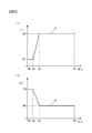
- FIG. 6 is a diagram showing a change over time in the pressure of the reaction gas and the electric power to be input in the plasma processing step.
- FIG. 6A is a diagram showing the change over time in the pressure of the reaction gas
- FIG. 6B is a diagram showing the change over time in the electric power supplied to the plasma generator.
- FIG. 7 is a diagram for explaining the formation of the metal oxide film 56 in the heat treatment.
- FIG. 1 is a diagram for explaining a plasma processing step and a seed layer deposition processing step for a processing object 50 containing an inorganic material such as glass.
- the processing object 50 is, for example, a substrate made of alkali-free glass, soda glass, or quartz glass, and a plurality of through holes 50h that connect the front surface 50c and the back surface 50d are formed. Note that at least a part of the through hole 50h may be a non-through hole that is formed only on the front surface 50c or the back surface 50d and does not penetrate the front surface 50c and the back surface 50d. A groove may be formed on the front surface 50c or the back surface 50d.
- the oxygen radical (O *) is irradiated not only on the front surface 50c and the back surface 50d of the processing object 50 but also on the inner surface of the through hole 50h, and activates these portions.
- a metal such as copper (Cu) is applied to the front surface 50c of the processing object 50 by a film forming method such as sputtering. Form a film. Details of the film forming method at this time will be described later. As will be described later, after the plasma processing shown in FIG. 1B is completed, the film-forming process shown in FIG. 1C is performed on the processing object 50 without being exposed to the atmosphere. As will be described later, in this film forming step, a metal film can also be formed on the inner surface of the through-hole 50 h formed in the processing object 50.
- the processing object 50 is inverted, and a metal such as copper (Cu) is formed on the back surface 50d of the processing object 50 and the inner surface of the through hole 50h, as shown in FIG.
- a metal such as copper (Cu)
- the processing order of the front surface 50c and the back surface 50d in the plasma processing and the film forming processing may be opposite to the order described above.
- seed layers are processed on the front surface 50c, the back surface 50d, and the inner side surfaces of the through holes 50h of the processing object 50. It is formed with high adhesion to the object 50. Further, the seed layers (metal films 51c and 51d) are also in close contact with the processing object 50 on the inner surfaces of the above-described non-through holes and grooves formed on the front surface 50c or the back surface 50d of the processing object 50. It is formed with sex.
- the state of the processing object 50 and the seed layers 51c and 51d shown in FIG. 1 (e) is referred to as a processing object 60 with a seed layer.
- the thickness of the metal film of the seed layers 51c and 51d is preferably about 100 nm to 1000 nm. If the thickness is less than 100 nm, the electrical resistance may be high and the function as a seed layer may not be sufficiently obtained. If the thickness is greater than 1000 nm, it takes time to form a film, resulting in an increase in manufacturing cost.
- the diameter of the through hole 50h is 20 ⁇ m to 50 ⁇ m in the vicinity of the front surface 50c and the back surface 50d, and 15 ⁇ m to 20 ⁇ m in the intermediate portion between the front surface 50c and the back surface 50d. That is, it is preferable that the inner diameter is large near the front surface 50c and the back surface 50d, and the inner diameter is relatively small inside.
- the seed layer (metal films 51c and 51d) is formed on all of the front surface 50c, the back surface 50d, and the inner surface of the through hole 50h of the processing object 50.
- the present invention is not limited to this. is not.
- the seed layers 51c and 51d can be formed in addition to the masked portions.
- the material of the seed layers 51c and 51d to be formed is not limited to copper, but may be an alloy containing copper, another metal such as nickel, aluminum, chromium, or an alloy containing them.
- FIG. 2A is a diagram showing the electrolytic plating process.
- the processing object 60 with the seed layer is immersed in the electrolytic solution 46 of the electrolytic plating apparatus 45, and the surface of the seed layers 51 c and 51 d has a power supply.
- the conducting wire 49a connected to 47 is connected.
- a counter electrode 48 is installed in the electrolytic solution 46, and a conductive wire 49 b connected to a power source 47 is connected to the counter electrode 48.
- the electrolytic solution 46 contains copper ions, and copper is deposited on the surfaces of the seed layers 51c and 51d of the processing object 60 with the seed layer by applying a potential lower than the conductive wire 49b to the conductive wire 49a by a predetermined potential difference. Then, electrolytic plating is performed.
- the counter electrode 48 a copper plate is used as an example. Since the electrolytic solution 46 penetrates into the through hole 50h and the seed layer is formed on the inner surface of the through hole 50h, copper is also plated inside the through hole 50h. Similarly, copper is also plated inside the non-through holes and grooves formed in the front surface 50c or the back surface 50d of the processing object 50 described above. In the plating process, the surface of the seed layers 51c and 51d can be partially plated by masking part of the surfaces of the seed layers 51c and 51d in advance.
- FIG. 2B shows the intermediate product 70 after the plating process.
- Copper plating films (metal films) 52c and 52d are applied to at least a part of the front surface 50c and the back surface 50d of the processing object 50, and copper 52e is plated on at least a part of the plurality of through holes 50h. Filled.
- the seed layers 51c and 51d are not shown.
- this plating process can also be performed not only by the above-mentioned electroplating but by electroless plating. Or it can also carry out by dry film-forming processes, such as vapor deposition, instead of plating.
- FIG. 3A shows a state where the intermediate product 70 is heat-treated.
- the heat treatment furnace 61 includes heaters 63 a and 63 b therein, and the heaters 63 a and 63 b are heated by electric power from the heating power source 62.
- the intermediate product 70 is heated and heat-treated by the heat from the heaters 63a and 63b.
- the surface of the object to be processed 50, the seed layers 51c and 51d, and the metal films 52c and 52d are bonded more firmly, and a strong conductive film with low electrical resistance is formed.
- an inert gas such as nitrogen may be supplied from the pipe 64 to the heat treatment furnace 61 in order to prevent thermal oxidation of the metal films 52c and 52d and the seed layers 51c and 51d.
- the gas in the heat treatment furnace 61 is exhausted from the pipe 65.
- This heat treatment is preferably performed for about 10 seconds to 24 hours at a temperature of 100 ° C. or higher up to the melting point of the object 50, the seed layers 51c and 51d, or the metal films 52c and 52d.
- a temperature of 100 ° C. or higher up to the melting point of the object 50, the seed layers 51c and 51d, or the metal films 52c and 52d When the temperature is lower than 100 ° C. or the processing time is shorter than 10 seconds, the bonding of the surface of the processing object 50, the seed layers 51 c and 51 d, and the metal films 52 c and 52 d does not proceed sufficiently, and the conductive material has strong and low resistance. It is difficult to obtain a film. Further, if the temperature is higher than the melting point of each constituent material, the processing object 50, the seed layers 51c and 51d and the metal films 52c and 52d may be deformed or damaged. Further, if the treatment time is longer than 24 hours, the productivity as a method for forming a conductive film may be reduced.
- the conductive film forming method of the embodiment is completed.
- the heating by this heat processing is set to the temperature increase rate of the grade which the process target object 50 containing inorganic materials, such as glass, does not deform
- the conductive film formed by the above-described method has strong adhesion with the processing object 50 made of an inorganic material such as glass, and the adhesion strength is about 5 N / cm or more as an example.
- the process target object 50 By patterning and removing a part of the conductive film (metal films 52c and 52d) from the process target object 50 on which the conductive films (metal films 52c and 52d) are formed by the above method, the process target object is obtained.
- 50 can be a wiring board having conductive films (metal films 52c and 52d) that remain without being removed as wiring layers.
- FIG. 3B is a diagram showing patterning on the conductive film (metal films 52c and 52d) of the intermediate product 70 after the heat treatment.
- a resist pattern 53 in which a desired pattern is formed by a lithography process is formed on the metal film 52c.
- the metal film 52c is etched into the wiring 54c shown in FIG. 3C by etching the metal film 52c using the resist pattern 53 as an etching mask.
- the wiring board 90 manufactured according to the present embodiment can be used as a wiring board for high-density mounting of semiconductor integrated circuits, for example, as an interposer.
- FIG. 4 shows a film forming apparatus used for the plasma processing step and the film forming step of the present embodiment.
- the film forming apparatus 100 includes a pressure resistant chamber 1 having a pressure resistant structure.
- the pressure resistant chamber 1 includes a plasma processing chamber 2 and a film forming processing chamber 3 separated by a partition wall 4.
- the partition 4 is provided with an opening 5 that connects the plasma processing chamber 2 and the film formation processing chamber 3, and the opening 5 can be opened and closed by an opening / closing door 6.
- the opening 5 and the open / close door 6 constitute an open / close configuration that opens and closes between the plasma processing chamber 2 and the film forming chamber 3.
- the film forming apparatus 100 further includes a control device 7.
- a plasma generation source having a high-density plasma electrode 12 and a counter electrode 14, and a frame portion 13 that holds the high-density plasma electrode 12 and the counter electrode 14 and forms a sealed space 22 therebetween. 15 is provided.
- a hollow cathode 12 can be used as an example of the high density plasma electrode 12.
- a first holding mechanism 23 is provided for holding the plasma processing object 50 a.
- a first decompression pump 25 is connected to the plasma processing chamber 2 via a decompression pipe 26, and the interior of the plasma processing chamber 2 is defined by the first decompression pump 25 and the decompression pipe 26 as a decompression mechanism. The pressure can be reduced.
- the first decompression pump 25 is controlled by a control signal S3 from the control device 7.
- FIG. 5 is a diagram showing the hollow cathode 12 viewed from the processing object 50a side in FIG.
- the hollow cathode 12 has a flat plate 12b made of a conductor such as metal, like a normal hollow cathode, and a number of hollow portions (through holes) 12a are formed in the plane.
- the hollow portions 12a are arranged on the square lattice and the centers of the squares constituting the square lattice, but the arrangement of the hollow portions 12a may be arbitrary.
- the hollow cathode 12 is connected to a plasma power source 19 through a power supply line 20.
- the plasma power source 19 for example, a power source that generates an AC voltage (mainly a negative voltage) at an RF frequency (eg, 13.56 MHz) is employed.
- the counter electrode 14 is grounded by a ground wiring 21.
- the film forming apparatus 100 includes a reaction gas supply pipe 16 connected to the sealed space 22, a reaction gas supply device 17 connected to the reaction gas supply pipe 16 extending outside the pressure-resistant chamber 1, and a reaction And a control valve 18 for controlling the pressure in the sealed space 22 by adjusting the flow rate of the reaction gas supplied from the gas supplier 17. Adjustment of the opening degree of the control valve 18 is controlled by a control signal S ⁇ b> 1 from the control device 7.
- the control valve 18 is provided in the reaction gas supplier 17.
- the reaction gas supplier 17 is supplied with, for example, a reaction gas via a factory pipe 28, but may be supplied from a gas cylinder.
- the film forming chamber 3 inside the pressure-resistant chamber 1 is provided with a second holding mechanism 35 for holding the object to be processed 50b, and a sputter electrode 33 composed of the electrode portion 31 and the target material 32.
- a sputter electrode 33 composed of the electrode portion 31 and the target material 32.
- the target material 32 copper is used as an example.
- the target material 32 aluminum, another metal, or an alloy containing the above metal can also be used.
- the sputter electrode 33 is connected to a sputtering power supply 34.
- the power supply 34 for sputtering can supply power of 10 kW or more, more desirably 30 kW or more, to the sputtering electrode 33.
- the sputtering power supply 34 is controlled by a control signal S 5 from the control device 7.
- the sputter electrode 33 or its electrode part 31 can also be interpreted as a film forming source for supplying a film material to be formed on the processing object 50b.
- a second decompression pump 36 is connected to the film formation processing chamber 3 via a decompression pipe 37, and the inside of the film formation treatment chamber 3 is connected by the second decompression pump 36 and the decompression pipe 37 as a decompression mechanism.
- the pressure can be reduced.
- the second decompression pump 36 is controlled by a control signal S4 from the control device 7.
- the film forming apparatus 100 further includes an inert gas supply pipe 41 that supplies an inert gas such as argon into the film forming chamber 3, an inert gas supply unit 38 connected to the inert gas supply pipe 41, And a control valve 39 for controlling the pressure in the film forming process chamber 3 by adjusting the flow rate of the inert gas supplied from the inert gas supply unit 38.
- an inert gas supply pipe 41 that supplies an inert gas such as argon into the film forming chamber 3
- an inert gas supply unit 38 connected to the inert gas supply pipe 41
- a control valve 39 for controlling the pressure in the film forming process
- the control valve 39 is provided in the inert gas supply unit 38.
- the adjustment of the opening degree of the control valve 39 is controlled by a control signal S6 from the control device 7.
- the inert gas supply unit 38 is supplied with an inert gas through, for example, a factory pipe 40, but may be supplied from a gas cylinder.
- the plasma processing step in the embodiment of the conductive film forming method will be described.
- the processing object 50a on which the conductive film is to be formed is carried into the plasma processing chamber 2 by a carrying mechanism (not shown) and held in the first holding mechanism 23. That is, the processing object 50a is disposed at a position away from the above-described plasma generation source 15 installed in the plasma processing chamber 2 in the pressure resistant chamber 1 by a distance d from the hollow cathode 12 to the side opposite to the counter electrode 14. Is done.
- the open / close door 6 between the plasma processing chamber 2 and the film forming processing chamber 3 is closed.
- the inside of the plasma processing chamber 2 is depressurized by a first depressurization pump 25 and a depressurization pipe 26 as a depressurization mechanism.
- the first pressure reducing pump 25 is controlled by a control signal S3 from the control device 7.
- the pressure reduction in the plasma processing chamber 2 is more than the arrangement of the processing object described above. Will be done before.
- the control device 7 sends a control signal S 1 to the control valve 18, thereby supplying a reaction gas having a predetermined pressure from the reaction gas supplier 17 to the sealed space 22 in the plasma generation source 15 through the reaction gas supply pipe 16.
- a reaction gas having a predetermined pressure For example, oxygen is used as the reaction gas, but nitrogen can also be used.
- the control device 7 sends a control signal S2 to the plasma power source 19, whereby the hollow cathode 12 is supplied to the hollow cathode 12 via the power supply line 20 by the plasma power source 19 through an AC / DC voltage (for example, 13.56 MHz). Mainly negative voltage) is applied.
- the counter electrode 14 is set to the ground potential by the ground wiring 21. As a result, a discharge is generated between the hollow cathode 12 and the counter electrode 14, and electrons generated by the discharge turn the reaction gas into plasma.
- the first holding mechanism 23 that holds the processing object 50 a is also set to the ground potential by the ground wiring 24.
- the distance d between the processing object 50a and the first holding mechanism 23 and the hollow cathode 12 is longer than the distance between the hollow cathode 12 and the counter electrode 14, the processing object 50a and the first holding mechanism 23 and the hollow
- the electric field between the cathode 12 is weak. Therefore, since most of the electrons discharged from the hollow cathode 12 flow into the counter electrode 14, the collision of the electrons with the object to be processed 50 a and the first holding mechanism 23 and heating them are hardly suppressed.
- the plasma generated by the plasma generation source 15 passes through the hollow portion 12a of the hollow cathode 12 and is emitted to the outside of the plasma generation source 15. Then, the plasma drifts in the plasma processing chamber 2 from the right to the left in FIG. 4 by the distance d and reaches the processing object 50a.
- the plasma generation is particularly likely to occur in the hollow portion 12 a provided in the hollow cathode 12.
- the plasma is hot at the stage of being emitted from the plasma generation source 15, the thermal energy is lost due to collision with the reaction gas existing in the plasma processing chamber 2 while drifting in the plasma processing chamber 2.
- the temperature of the plasma is lowered.
- a part of the plasma is changed from the plasma (charged state) to the activated state (radical state) due to collision with the reaction gas. Therefore, the processing object 50a is exposed not only to the reactive gas plasma but also to the activated (radical) reactive gas.
- the reaction gas in the plasma state and the reaction gas in the activated state (radical state) are referred to as a highly reactive reaction gas.
- activating the surface of the processing object 50a with a reactive gas in a plasma state or a reactive gas in a radical state is called plasma processing.
- the effect that the temperature of the plasma is lowered and the reaction gas in the radical state also reaches when the object 50a reaches the object 50a is that the object 50a is moved from the hollow cathode 12 to the side opposite to the counter electrode 14. This is because it is provided at a distant position.
- the processing object 50a and the counter electrode 14 sandwich the hollow cathode 12 so that the distance d between the hollow cathode 12 and the processing object 50a is set longer than the distance between the hollow cathode 12 and the counter electrode 14. Has been placed.
- the concentration of the highly reactive reaction gas that reaches the processing object 50a may be reduced.
- the plasma generated in the plasma generation source 15 since the space between the plasma generation source 15 and the processing object 50a is depressurized, the plasma generated in the plasma generation source 15 generates more gas molecules (reactive gas) than necessary. Can be prevented from lowering the concentration of the highly reactive gas.
- the surface of the object 50a to be processed is activated by the plasma treatment, and the bondability with the metal atom is improved.
- the hydrophilicity of the surface of the glass constituting the object to be processed 50a is increased by plasma treatment (electrical polarity is increased), thereby improving the bondability with metal atoms.
- FIG. 6A is a diagram showing the time change of the pressure P of the reaction gas in the plasma generation source 15, and FIG. 6B is a diagram showing the time change of the electric power E applied to the hollow cathode 12. .
- the control device 7 adjusts the opening of the control valve 18 provided in the reaction gas supply 17 by the control signal S1, and the reaction in the plasma generation source 15 is performed.
- the gas pressure is set to be the first pressure P1.
- the control device 7 adjusts the plasma power supply 19 based on the control signal S ⁇ b> 2 and applies the power of the first output E ⁇ b> 1 to the hollow cathode 12. As a result, a discharge is generated between the hollow cathode 12 and the counter electrode 14, and a first plasma state is formed in the plasma generation source 15.
- the first pressure P1 and the first output E1 are set to conditions that can form plasma efficiently in accordance with the shape of the hollow cathode 12 to be used (diameter in the hollow portion 12a). In other words, it can be said that it is preferable to set the shape or the like of the hollow cathode 12 to be used in such a condition that plasma can be efficiently formed according to the first pressure P1 and the first output E1.
- the control device 7 opens (increases) the opening of the control valve 18 so that the pressure P of the reactive gas in the plasma generation source 15 is set to the first plasma state.
- a control signal S1 is sent to set the second pressure P2 higher than the pressure P1.
- the control device 7 sends a control signal S2 for reducing the power E applied to the hollow cathode 12 to the plasma power source 19 to a second output E2 lower than the first output E1.
- the pressure P of the reaction gas in the plasma generation source 15 becomes the second pressure P2, and the power applied to the hollow cathode 12 is set to the second output E2.
- the plasma generation source 15 No new plasma is formed inside.
- the discharge can be continued even under a high second pressure P2, and a high-density second plasma state is formed. be able to.
- Plasma treatment By exposing the object 50a to the highly reactive reaction gas composed of the reaction gas in the plasma state and the reaction gas in the activated state (radical state) generated in the first plasma state and the second plasma state. Then, plasma processing of the processing object 50a is performed. At time t3, the control device 7 stops the supply of the reactive gas into the plasma generation source 15 or reduces the supply amount, stops the application of power to the hollow cathode 12, and ends the plasma processing.
- both the front surface 50c and the back surface 50d of the processing object 50a are plasma-processed. Therefore, between the time t2 and the time t3, the front surface 50c and the back surface 50d of the processing object 50a are reversed by the first holding mechanism 23.
- the front surface 50c and the back surface 50d of the processing object 50a are reversed by the first holding mechanism 23.
- the process from time t1 to time t3 may be performed again.
- said 1st pressure P1 is a pressure of 0.1 Pa or more and 50 Pa or less, for example.
- said pressure is lower than 0.1 Pa, the initial plasma concentration becomes thin, and it becomes difficult to maintain a stable discharge.
- the pressure is higher than 50 Pa, it is difficult to discharge.
- said 2nd pressure P2 is a pressure of 1 Pa or more and 100 Pa or less, for example.
- the pressure is lower than 1 Pa, the plasma concentration becomes thin and it becomes difficult to exhibit high processing capability.
- the pressure is higher than 100 Pa, it is difficult to maintain the discharge.
- the 1st output E1 which is the electric power applied to the hollow cathode 12 at the time of formation of a 1st plasma state is 2 W / cm ⁇ 2 > or more and 5 W / cm ⁇ 2 > or less per unit area of the hollow cathode 12. If the first output E1 is smaller than 2 W / cm 2 , it is difficult to generate plasma by generating discharge in the plasma generation source 15. On the other hand, if the first output E1 is greater than 5 W / cm 2 , abnormal discharge may occur in the plasma generation source 15.
- the second output E2 which is the power applied to the hollow cathode 12 when the second plasma state is formed, is preferably 0.5 W / cm 2 or more and 2 W / cm 2 or less per unit area of the hollow cathode 12. . If the second output E2 is smaller than 0.5 W / cm 2 , it becomes difficult to maintain discharge and plasma formation in the plasma generation source 15. On the other hand, if the first output E1 is greater than 2 W / cm 2 , abnormal discharge may occur in the plasma generation source 15.
- the distance d from the hollow cathode 12 to the object to be treated 50a is preferably 50 mm or more and 300 mm or less. If the distance d is shorter than 50 mm, the processing object 50a may be heated to a high temperature. If the distance d is longer than 300 mm, the plasma concentration becomes thin and it becomes difficult to exhibit high processing capability.
- the duration of the second plasma state (time from time t2 to time t3) is preferably 10 times or more of the duration of the first plasma state (time from time t0 to time t1). Since the second plasma state can generate a highly reactive gas having a higher concentration than the first plasma state, the second plasma state can be generated more efficiently, that is, productivity. High film formation method can be realized.
- the processing object 50a for which the plasma processing has been completed is not exposed to the atmosphere from the first holding mechanism 23 in the plasma processing chamber 2 by the transfer mechanism 30 provided in the plasma processing chamber 2.
- the second holding mechanism 35 is conveyed.
- the controller 7 sends a control signal S4 to the second decompression pump 36 to decompress the interior of the film forming process chamber 3.
- the door 6 is opened during the conveyance, and the door 6 is closed after the conveyance is completed.
- the processing object 50a is held by the second holding mechanism 35 in the film formation processing chamber 3.
- the processing object 50a that is transported and held by the second holding mechanism 35 in the film formation processing chamber 3 is referred to as a processing object 50b.
- the inert gas in the vicinity of the sputtering electrode 33 in the film forming chamber 3 is ionized, accelerated by the electric field of the sputtering electrode 33 and collides with the target material 32, and atoms of copper or other metal constituting the target material 32. Is discharged into the film forming chamber 3 and is deposited on the processing object 50b.
- a metal atom is formed on the surface of the processing object 50b activated by the above-described plasma treatment while the activated portion is not inactivated by water vapor or oxygen in the atmosphere. Therefore, a metal film having a high binding property to the processing object 50b, that is, a high adhesion property is formed.
- the film is generally formed by reducing the pressure in the sputtering apparatus to about 0.1 Pa. If the pressure in the sputtering apparatus is higher than this, it is difficult to remove impurities such as water remaining in the sputtering apparatus or discharged from the object to be processed. As a result, impurities are mixed into the film and the quality of the film is deteriorated. It is because it falls.
- the pressure in the film forming chamber 3 is set to about 0.5 Pa to 10 Pa.
- the metal atoms ejected from the target material 32 can be collided with the inert gas molecules in the film forming chamber 3 at a high frequency, and the straightness of the metal atoms is reduced, that is, the progress of the metal atoms.
- the direction can be diffused. Accordingly, a uniform film can be formed even on the processing object 50b having an uneven shape.
- a metal film can be formed also on the inner surface of the through hole 50h shown in FIGS. 1 (c) and 1 (d).
- the pressure in the film formation chamber 3 is 0.5 Pa or less, it is difficult to sufficiently scatter metal atoms when being released from the target material 32.
- the pressure is about 10 Pa or more, the concentration of impurities in the film formation chamber 3 May increase and the quality of the film may deteriorate.
- the pressure in the film forming chamber 3 is set higher than the conventional pressure (about 0.5 Pa to 10 Pa), there is a concern that impurities are mixed into the film to be formed.
- mixing of impurities is prevented by applying high power of 10 kW or more, more desirably 30 kW or more, to the sputter electrode 33.
- the power supplied to the sputter electrode 33 When the power supplied to the sputter electrode 33 is large, the amount of metal atoms such as copper released from the target material 32 is increased and the movement of the metal atoms compared to the case where normal power is supplied. Energy also increases. As a result, in this embodiment, the purity of the film formed on the processing object 50b is improved by reducing the concentration of impurities in the film formation processing chamber 3 relative to the concentration of metal atoms. Furthermore, since the kinetic energy of the metal atom that collides with the object to be processed 50b is large, the molecules constituting the object to be processed 50b and the metal atom are stably bonded, and thus the film having higher adhesion to the object to be processed 50b. Can be formed.
- the film forming process is performed on both the front surface 50c and the back surface 50d of the processing object 50a.
- the front surface 50c and the back surface 50d of the processing object 50a are reversed by the second holding mechanism 35, and the processing object is processed. This is also performed on the rear surface 50d of 50a.
- the object to be processed 50b after film formation is unloaded from the film formation chamber 3 by an unillustrated unloading mechanism.
- the unloading mechanism (not shown) preferably has a load lock chamber.
- the open / close door 6 between the plasma processing chamber 2 and the film forming processing chamber 3 is closed.
- the plasma processing and the film forming process are respectively performed in the plasma processing chamber 2 and the film forming processing chamber 3 which are both in the pressure-resistant chamber 1 and partitioned by the partition wall 4.
- the place where each process is performed is not limited to this.
- plasma processing and film formation processing may be performed in the pressure resistant chamber 1 without the partition 4.
- the plasma treatment and the film formation treatment can be performed in separate pressure resistant chambers.
- the pressure is reduced between the plasma processing chamber 2 and the film-forming processing chamber 3. It is desirable to provide a transfer path that can replace the gas with an inert gas.
- the pressure in each processing chamber can be controlled independently.
- the plasma treatment and the film formation treatment can be performed in parallel, and the conductive film can be formed with higher processing ability.
- the mutual contamination between the plasma treatment and the film formation treatment can be minimized, the quality of the film to be formed can be further improved.
- the film formation is performed by sputtering.
- the present invention is not limited to this, and the film formation can also be performed using vapor deposition or CVD.
- the metal materials to be formed include copper, nickel, chromium, platinum, gold, palladium, titanium, chromium alloy, stainless steel alloy, aluminum, aluminum alloy, nickel alloy, titanium alloy, copper alloy, tantalum, tantalum alloy, silver At least one of silver alloy, tin, tin alloy, gold, gold alloy, platinum alloy, palladium alloy, silicon, silicon alloy, cobalt, cobalt alloy, niobium, niobium alloy, indium, indium alloy, tungsten, tungsten alloy Metal materials can be used.
- FIG. 7 is a diagram for explaining the formation of the metal oxide film 56 in the heat treatment.
- 7A shows a state before the heat treatment of the seed layer 51c and the copper plating film (metal film) 52c formed on the front surface of the intermediate product 70
- FIG. 7B shows the state after the heat treatment.
- a boundary layer 55a is formed that includes a deformed material that has undergone alteration such as oxidation due to the above-described plasma treatment.
- Deformants that have undergone alteration such as oxidation by plasma treatment include oxides of the composition of the object to be treated 50 and molecular structures constituting the composition of the object to be treated 50 partially cut by the plasma treatment. Some (eg functional groups) are also included.
- the processing object 50 on which the seed layer 51c and the metal film 52c are formed is heat-treated (annealed)
- oxygen contained in the boundary layer 55a reacts with metal atoms in the seed layer 51c by heat.
- a metal oxide layer 56 mainly composed of a metal oxide constituting the seed layer 51c is formed.
- the metal oxide layer 56 is also referred to as a first layer 56.
- a part of oxygen contained in the boundary layer 55a is lost from the boundary layer 55a by reaction with the metal atoms in the seed layer 51c, so that the thickness of the boundary layer 55a is reduced by the heat treatment.
- the boundary layer 55 after the heat treatment is also referred to as a second layer 55.
- the adhesion of the seed layer 51c to the object to be processed 50 is such that the seed layer 51c causes the first layer 56 and the second layer 55 to adhere to a state before the heat treatment in which the seed layer 51c is bonded only through the boundary layer 55a.
- the state after the heat treatment that is joined via is stronger. For this reason, the contact
- the change before and after the heat treatment of the seed layer 51d formed on the back surface 50d of the intermediate product 70 is the same as that of the seed layer 51c formed on the front surface 50c.
- the materials constituting the seed layers 51c and 51d are as follows: A metal having high reactivity with oxygen is preferable.
- the seed layers 51c and 51d are made of copper, nickel, chromium, titanium, chromium alloy, stainless steel alloy, aluminum, aluminum alloy, titanium alloy, copper alloy, tantalum, tantalum alloy, tin, tin alloy, silicon, silicon alloy, It is preferable to form a film using a metal material containing at least one of niobium, niobium alloy, indium, indium alloy, tungsten, and tungsten alloy.
- the thickness T53 of the first layer 56 is more preferably 0.5 nm or more.
- the thickness T56 of the first layer 56 is more preferably 5 nm or less.
- the thickness T55 of the second layer 55 is more preferably 2 nm or more.
- the thickness T55 of the second layer 55 is more preferably 5 nm or less.
- a product in which the first layer 56 is formed between the processing object 50 and the seed layers 51c and 51d by heat treatment is referred to as an intermediate product 71 with a first layer.
- the conductive film can be patterned on the intermediate product 71 with the first layer.
- a plasma generation source including a high-density plasma electrode 12 and a counter electrode 14 disposed facing the high-density plasma electrode 12 installed in the pressure-resistant chamber 1.
- the processing object 50 is disposed at a position away from the high-density plasma electrode 12 on the side opposite to the counter electrode 14, the pressure inside the pressure-resistant chamber 1 is reduced, and a reactive gas is supplied to the plasma generation source 15.
- Forming the plasma state exposing the processing object 50a to the reactive gas made highly reactive in the plasma generation source 15, and exposing the processing object 50 exposed to the reaction gas to the atmosphere without exposing it to the atmosphere.
- the seed layers 51c and 51d are formed on at least a part of the surface of the substrate, and the electroless plating is applied on at least a part of the surface of the seed layers 51c and 51d formed on the processing target 50.
- the surface of the processing object 50 can be activated while preventing the processing object 50 from being rapidly or locally heated.
- seed layers 51 c and 51 d having high adhesion to the processing object 50 can be formed on the surface of the processing object 50. Further, the heat treatment after the formation of the metal films 52c and 52d can further improve the adhesion between the processing object 50, the seed layers 51c and 51d, and the metal films 52c and 52d, and the conductive layer has high adhesion and is difficult to peel off. Can be formed.
- plasma with higher density can be formed, the processing time of the plasma processing can be shortened, and the processing capability can be further improved.
- the seed layer can also be formed by sputtering with a power of 10 kW or more applied to the sputtering electrode. As a result, a high-quality conductive layer with less impurities can be formed.
- a uniform conductive layer is formed even on the processing object 50 having a concavo-convex shape by performing sputtering at an atmospheric pressure in the pressure resistant chamber of 0.5 Pa or more and 10 Pa or less. Can do.
- the seed layers 51c and 51d are made of copper, nickel, chromium, titanium, chromium alloy, stainless steel alloy, aluminum, aluminum alloy, nickel alloy, titanium alloy, copper alloy, tantalum, tantalum alloy, tin, tin alloy, silicon,
- a metal material including at least one of silicon alloy, niobium, niobium alloy, indium, indium alloy, tungsten, and tungsten alloy
- the seed layers 51c and 51d and the object to be processed 50 are formed in the heat treatment.
- an oxide layer (first layer 56) of a metal material can be formed. Thereby, the adhesiveness between seed layer 51c, 51d and the process target object 50 can be improved further.
- the embodiment of the above-described method for manufacturing a wiring board includes preparing a substrate and forming a conductive film on the substrate by the embodiment of the conductive film forming method. With such a configuration, it is possible to realize a wiring substrate having a wiring layer having high adhesion to a substrate made of an inorganic material such as glass.
- 100 film forming apparatus, 1: pressure-resistant chamber, 2: plasma processing chamber, 3: film forming processing chamber, 7: control device, 12: high-density plasma electrode (hollow cathode), 14: counter electrode, 15: plasma generation source, 16: reactive gas supply pipe, 17: reactive gas supplier, 18: control valve, 19: plasma power source, 23: first holding mechanism, 25: first decompression pump, 33: plasma electrode, 34: power source for sputtering, 35: second holding mechanism, 36: second decompression pump, 45: electrolytic plating apparatus, 61: heat treatment furnace, 50, 50a, 50b: treatment object, 51c, 51d: seed layer, 52c, 52d: metal film, 70 : Intermediate product, 90: Wiring board
Landscapes
- Chemical & Material Sciences (AREA)
- Engineering & Computer Science (AREA)
- Organic Chemistry (AREA)
- Materials Engineering (AREA)
- Mechanical Engineering (AREA)
- Metallurgy (AREA)
- Chemical Kinetics & Catalysis (AREA)
- Manufacturing & Machinery (AREA)
- Microelectronics & Electronic Packaging (AREA)
- Physical Vapour Deposition (AREA)
- Electrodes Of Semiconductors (AREA)
- Internal Circuitry In Semiconductor Integrated Circuit Devices (AREA)
- Manufacturing Of Printed Wiring (AREA)
Abstract
導電膜形成方法は、耐圧チャンバ内に設置されている高密度プラズマ発生源から離れた位置に処理対象物を配置すること、耐圧チャンバ内を減圧すること、プラズマ発生源に反応ガスを供給してプラズマ状態を形成すること、処理対象物をプラズマ発生源において高反応性化された反応ガスに晒すこと、反応ガスに晒した処理対象物を大気に晒すことなく処理対象物の表面の一部にシード層を成膜すること、処理対象物に成膜されたシード層の表面の一部に、無電解めっき、電解めっき、またはドライ成膜プロセスにより金属膜を形成すること、シード層および金属膜が形成された処理対象物を熱処理すること、とを含む。
Description
本発明は、導電膜形成方法、および配線基板の製造方法に関する。
ガラスなどの無機材料からなる絶縁体の表面に金属めっきにより導電膜を形成するために、絶縁体の表面に無電解めっきによりシード層と呼ばれる薄い導電層を形成し、このシード層を電極としてシード層の上に金属を電解めっきすることが行われている。
絶縁体の表面へのシード層の形成方法として、絶縁体の表面にエッチング処理等で微小な凹凸を形成し、そこにパラジウム等の触媒を添加したうえで、無電解めっきを行うことが知られている(特許文献1)。
一方、樹脂に対して金属膜を成膜する際に、プラズマ処理により樹脂の表面に金属との密着性を高めるための化合物層を形成し、その化合物層の上に金属膜を形成する成膜方法および成膜装置も提案されている(特許文献2)。
絶縁体の表面へのシード層の形成方法として、絶縁体の表面にエッチング処理等で微小な凹凸を形成し、そこにパラジウム等の触媒を添加したうえで、無電解めっきを行うことが知られている(特許文献1)。
一方、樹脂に対して金属膜を成膜する際に、プラズマ処理により樹脂の表面に金属との密着性を高めるための化合物層を形成し、その化合物層の上に金属膜を形成する成膜方法および成膜装置も提案されている(特許文献2)。
一般に、プラズマ処理は、反応ガスを満たした2つの電極間に高電圧を印加して放電を行うことによりプラズマ化した反応ガスを用いて行う。従来においては、2つの電極間に処理対象物を配置し、電極間の放電により生じたプラズマを処理対象物に照射することが一般的である。処理対象物自体または処理対象物を保持する金属製の保持機構を、2つの電極のうち一方として使用する場合もある。
特許文献3には、放電のための2つの電極の外部に処理対象物を配置するプラズマ発生装置も提案されている。
特許文献3には、放電のための2つの電極の外部に処理対象物を配置するプラズマ発生装置も提案されている。
導電膜の形成に使用する従来のめっき方法においては、絶縁体の基材とめっき膜との密着性が十分でなく、剥離が生じ易いという課題がある。
また、特許文献2に開示されるような成膜方法および成膜装置は、プラズマにより樹脂の表面に樹脂および金属との密着性が良好な化合物層を形成するものであり、樹脂とは化学的な性質が異なるガラス等の無機材料に対して適用することは困難である。さらに、ガラス等の無機材料はプラズマの照射による急激または局所的な温度変化に弱いという問題もある。
一方、特許文献3に開示されるプラズマ処理装置は、処理対象物の温度上昇を押さえることはできるが、処理対象物を大気圧下に配置して処理を行うものであり、高処理能力の処理を行うことは困難である。
また、特許文献2に開示されるような成膜方法および成膜装置は、プラズマにより樹脂の表面に樹脂および金属との密着性が良好な化合物層を形成するものであり、樹脂とは化学的な性質が異なるガラス等の無機材料に対して適用することは困難である。さらに、ガラス等の無機材料はプラズマの照射による急激または局所的な温度変化に弱いという問題もある。
一方、特許文献3に開示されるプラズマ処理装置は、処理対象物の温度上昇を押さえることはできるが、処理対象物を大気圧下に配置して処理を行うものであり、高処理能力の処理を行うことは困難である。
第1の態様の導電膜形成方法は、耐圧チャンバ内に設置されている、高密度プラズマ電極および前記高密度プラズマ電極に対向して配置されている対極を含むプラズマ発生源に対し、前記高密度プラズマ電極から前記対極とは反対側に離れた位置に、処理対象物を配置すること、前記耐圧チャンバ内を減圧すること、前記プラズマ発生源に反応ガスを供給してプラズマ状態を形成すること、前記処理対象物を、前記プラズマ発生源において高反応性化された前記反応ガスに晒すこと、前記反応ガスに晒した前記処理対象物を大気に晒すことなく、前記処理対象物の表面の少なくとも一部にシード層を成膜すること、前記処理対象物に成膜された前記シード層の表面の少なくとも一部に、電解めっき、無電解めっき、またはドライ成膜プロセスにより金属膜を形成すること、前記シード層および前記金属膜が形成された前記処理対象物を熱処理すること、とを含む。
第2の態様の配線基板の製造方法は、基板を用意すること、前記基板に第1の態様の導電膜形成方法により導電膜を形成すること、とを含む。
第2の態様の配線基板の製造方法は、基板を用意すること、前記基板に第1の態様の導電膜形成方法により導電膜を形成すること、とを含む。
本発明によれば、ガラス等の無機材料に対して密着性の高い膜を形成する高処理能力の導電膜形成方法および配線基板の製造方法を実現できる。
(導電膜形成方法の実施形態の概要)
図1から図3を参照して、実施形態の導電膜形成方法の概要を説明する。
図1は、ガラス等の無機材料を含む処理対象物50に対する、プラズマ処理工程およびシード層の成膜処理工程を説明する図である。
図1から図3を参照して、実施形態の導電膜形成方法の概要を説明する。
図1は、ガラス等の無機材料を含む処理対象物50に対する、プラズマ処理工程およびシード層の成膜処理工程を説明する図である。
始めに、図1(a)に示すとおり、処理対象物50のおもて面50cに対して酸素ラジカル(O*)および酸素プラズマ等を用いたプラズマ処理を行なう。プラズマ処理の詳細については、後述する。
処理対象物50は、一例として無アルカリガラス、ソーダガラス、または石英ガラスからなる基板であり、おもて面50cと裏面50dをつなぐ貫通孔50hが複数形成されている。
なお、貫通孔50hの少なくとも一部は、おもて面50cまたは裏面50dのみに形成され、おもて面50cと裏面50dを貫通しない非貫通孔であっても良い。また、おもて面50cまたは裏面50dに、溝が形成されていても良い。
次に、処理対象物50を反転させ、図4(b)に示すとおり、裏面50dをプラズマ処理する。酸素ラジカル(O*)は、処理対象物50のおもて面50cおよび裏面50dのみでなく、貫通孔50hの内側面にも照射され、これらの部分を活性化する。
処理対象物50は、一例として無アルカリガラス、ソーダガラス、または石英ガラスからなる基板であり、おもて面50cと裏面50dをつなぐ貫通孔50hが複数形成されている。
なお、貫通孔50hの少なくとも一部は、おもて面50cまたは裏面50dのみに形成され、おもて面50cと裏面50dを貫通しない非貫通孔であっても良い。また、おもて面50cまたは裏面50dに、溝が形成されていても良い。
次に、処理対象物50を反転させ、図4(b)に示すとおり、裏面50dをプラズマ処理する。酸素ラジカル(O*)は、処理対象物50のおもて面50cおよび裏面50dのみでなく、貫通孔50hの内側面にも照射され、これらの部分を活性化する。
処理対象物50へのプラズマ処理の終了後に、図1(c)に示すとおり、処理対象物50のおもて面50cに対して、スパッタリング等の成膜方法により銅(Cu)等の金属を成膜する。この際の成膜方法についても詳細は後述する。後述するとおり、図1(b)に示すプラズマ処理の終了後、処理対象物50は、大気に晒されることなく、図1(c)に示す成膜処理が行われる。
後述するとおり、この成膜工程においては、処理対象物50に形成されている貫通孔50hの内側面にも、金属を成膜することができる。
後述するとおり、この成膜工程においては、処理対象物50に形成されている貫通孔50hの内側面にも、金属を成膜することができる。
次に、処理対象物50を反転させ、図1(d)に示すとおり、処理対象物50の裏面50dおよび貫通孔50hの内側面に、銅(Cu)等の金属を成膜する。
プラズマ処理および成膜処理における、おもて面50cと裏面50dの処理順は、それぞれ上述の順とは逆であっても良い。
プラズマ処理および成膜処理における、おもて面50cと裏面50dの処理順は、それぞれ上述の順とは逆であっても良い。
以上の工程により、図1(e)に示すとおり、処理対象物50のおもて面50c、裏面50d、および貫通孔50hの内側面には、シード層(金属膜51c、51d)が処理対象物50と高い密着性をもって形成される。また、処理対象物50のおもて面50cまたは裏面50dに形成されている上述の非貫通孔および溝の内側面にも、シード層(金属膜51c、51d)が処理対象物50と高い密着性をもって形成される。図1(e)に示す処理対象物50およびシード層51c、51dの状態を、シード層付処理対象物60と呼ぶ。
シード層51c、51dの金属膜の厚さは、100nmから1000nm程度であることが好ましい。100nmより薄い場合には電気抵抗が大きくシード層としての機能が十分に得られない恐れがあり、1000nmより厚い場合には成膜に時間を要し、製造コストが上昇する問題がある。
また、貫通孔50hの直径は、おもて面50cおよび裏面50d付近において20μmから50μmとし、おもて面50cと裏面50dとの中間部分においては、15μmから20μmとする。すなわち、おもて面50cおよび裏面50d付近では内径が大きく、内部では内径を相対的に小さくすることが好ましい。
また、貫通孔50hの直径は、おもて面50cおよび裏面50d付近において20μmから50μmとし、おもて面50cと裏面50dとの中間部分においては、15μmから20μmとする。すなわち、おもて面50cおよび裏面50d付近では内径が大きく、内部では内径を相対的に小さくすることが好ましい。
なお、上記では処理対象物50のおもて面50c、裏面50d、および貫通孔50hの内側面の全ての部分にシード層(金属膜51c、51d)を形成しているが、これに限るわけではない。例えば、成膜処理に先立って、処理対象物50の表面(おもて面50c、裏面50d)の一部をマスキングすることで、マスキングした部分以外にシード層51c、51dを形成することもできる。
また、形成するシード層51c、51dの材料としては、銅に限らず、銅を含む合金や、ニッケル、アルミニウム、クロム等の他の金属およびそれらを含む合金であっても良い。
また、形成するシード層51c、51dの材料としては、銅に限らず、銅を含む合金や、ニッケル、アルミニウム、クロム等の他の金属およびそれらを含む合金であっても良い。
次に、シード層51c、51dの形成されたシード層付処理対象物60の表面の少なくとも一部に、電解めっきによりさらに銅等の金属の膜を形成する。
図2(a)は、この電解めっきの工程を表す図であり、シード層付処理対象物60は電解めっき装置45の電解液46中に浸され、シード層51c、51dの表面には、電源47に接続されている導線49aが接続されている。電解液46中には、対向電極48が設置されており、対向電極48には、電源47に接続されている導線49bが接続されている。
図2(a)は、この電解めっきの工程を表す図であり、シード層付処理対象物60は電解めっき装置45の電解液46中に浸され、シード層51c、51dの表面には、電源47に接続されている導線49aが接続されている。電解液46中には、対向電極48が設置されており、対向電極48には、電源47に接続されている導線49bが接続されている。
電解液46は一例として銅イオンを含み、導線49aに導線49bよりも所定の電位差だけ低い電位を印加することにより、シード層付処理対象物60のシード層51c、51dの表面に銅が析出して、電解めっきが行われる。対向電極48としては、一例として銅板を使用する。電解液46は貫通孔50hの内部にも浸透し、また貫通孔50hの内側面にもシード層が形成されているので、貫通孔50hの内部にも銅がめっきされる。同様に、上述の処理対象物50のおもて面50cまたは裏面50dに形成されている非貫通孔および溝の内部にも、銅がめっきされる。
なお、めっき工程に際しても、事前にシード層51c、51dの表面の一部をマスクキングすることにより、シード層51c、51dの表面に部分的にめっきを施すこともできる。
なお、めっき工程に際しても、事前にシード層51c、51dの表面の一部をマスクキングすることにより、シード層51c、51dの表面に部分的にめっきを施すこともできる。
図2(b)に、めっき工程が終了した中間製品70を示す。
処理対象物50のおもて面50c、裏面50dの少なくとも一部には、銅めっき膜(金属膜)52c、52dが施され、複数の貫通孔50hの少なくとも一部にもめっきにより銅52eが充填されている。なお、図2(b)では、シード層51c、51dは図示を省略している。
なお、このめっき工程は、上述の電解めっきに限らず、無電解めっきにより行うこともできる。あるいは、めっきでなく、蒸着等のドライ成膜プロセスにより行うこともできる。
処理対象物50のおもて面50c、裏面50dの少なくとも一部には、銅めっき膜(金属膜)52c、52dが施され、複数の貫通孔50hの少なくとも一部にもめっきにより銅52eが充填されている。なお、図2(b)では、シード層51c、51dは図示を省略している。
なお、このめっき工程は、上述の電解めっきに限らず、無電解めっきにより行うこともできる。あるいは、めっきでなく、蒸着等のドライ成膜プロセスにより行うこともできる。
次に、金属膜52c、52dの形成された中間製品70に対して、熱処理(アニール)を行う。
図3(a)は、中間製品70を熱処理している状態を示す。
熱処理炉61は、その内部にヒータ63a、63bを備え、ヒータ63a、63bは加熱電源62からの電力により加熱される。ヒータ63a、63bからの熱により、中間製品70は加熱され、熱処理される。
図3(a)は、中間製品70を熱処理している状態を示す。
熱処理炉61は、その内部にヒータ63a、63bを備え、ヒータ63a、63bは加熱電源62からの電力により加熱される。ヒータ63a、63bからの熱により、中間製品70は加熱され、熱処理される。
この熱処理により、処理対象物50の表面、シード層51c、51d、および金属膜52c、52dは、一層強固に結合され、丈夫で剥離しにくく、かつ電気抵抗の低い導電膜が形成される。
熱処理に際し、金属膜52c、52dおよびシード層51c、51dの熱酸化を防止するために、熱処理炉61に対して配管64から窒素等の不活性ガスを供給しても良い。熱処理炉61内の気体は、配管65から排気される。
熱処理に際し、金属膜52c、52dおよびシード層51c、51dの熱酸化を防止するために、熱処理炉61に対して配管64から窒素等の不活性ガスを供給しても良い。熱処理炉61内の気体は、配管65から排気される。
この熱処理は、100℃以上であって処理対象物50、シード層51c、51d、または金属膜52c、52dの融点までの温度において、10秒から24時間程度行うことが好ましい。温度が100℃より低い、または処理時間が10秒より短いと、処理対象物50の表面、シード層51c、51d、および金属膜52c、52dの結合が十分に進まず、強固で低抵抗の導電膜を得難い。また温度が各構成材料の融点より高いと処理対象物50、シード層51c、51dおよび金属膜52c、52dが変形または破損する恐れがある。また、処理時間が24時間より長いと、導電膜形成方法としての生産性が低下する恐れがある。
この熱処理により、実施形態の導電膜形成方法は完了する。
なお、この熱処理による加熱は、ガラス等の無機材料を含む処理対象物50が変形および破損しない程度の温度上昇速度に設定する。
上述の方法により形成された導電膜は、ガラスなどの無機材料からなる処理対象物50との間で強固な密着性を有し、その密着強度は、一例として5N/cm程度以上となる。
なお、この熱処理による加熱は、ガラス等の無機材料を含む処理対象物50が変形および破損しない程度の温度上昇速度に設定する。
上述の方法により形成された導電膜は、ガラスなどの無機材料からなる処理対象物50との間で強固な密着性を有し、その密着強度は、一例として5N/cm程度以上となる。
(配線基板の製造方法の実施形態の概要)
上記の方法により導電膜(金属膜52c、52d)が形成された処理対象物50に対して、その導電膜(金属膜52c、52d)の一部をパターニングして除去することにより、処理対象物50を、除去されずに残留した導電膜(金属膜52c、52d)を配線層として有する配線基板とすることができる。
上記の方法により導電膜(金属膜52c、52d)が形成された処理対象物50に対して、その導電膜(金属膜52c、52d)の一部をパターニングして除去することにより、処理対象物50を、除去されずに残留した導電膜(金属膜52c、52d)を配線層として有する配線基板とすることができる。
図3(b)は、熱処理後の中間製品70の導電膜(金属膜52c、52d)に対するパターニングを示す図である。金属膜52cの上には、リソグラフィ工程により所望のパターンが形成されたレジストパターン53が形成されている。そして、このレジストパターン53をエッチングマスクとして、金属膜52cをエッチングすることにより、金属膜52cは、図3(c)に示す配線54cにパターニングされる。
不図示ではあるが、図3(b)の金属膜52dに対しても、同様のパターニングが行われ、図3(c)に示す配線54dが形成される。
これにより、図3(c)に示すとおり、配線基板90が完成する。
本実施形態により製造された配線基板90は、例えば、インターポーザとして、半導体集積回路の高密度実装のための配線基板として使用することができる。
これにより、図3(c)に示すとおり、配線基板90が完成する。
本実施形態により製造された配線基板90は、例えば、インターポーザとして、半導体集積回路の高密度実装のための配線基板として使用することができる。
(プラズマ処理工程およびスパッタ成膜工程)
以下、図4から図6を参照して、本実施形態のうちの、プラズマ処理工程と成膜工程について説明する。
以下、図4から図6を参照して、本実施形態のうちの、プラズマ処理工程と成膜工程について説明する。
(プラズマ処理工程およびスパッタ成膜工程で用いる装置)
図4は、本実施形態のプラズマ処理工程と成膜工程に使用する成膜装置を示す。
成膜装置100は耐圧構造の耐圧チャンバ1を備え、耐圧チャンバ1の内部には、隔壁4により隔てられたプラズマ処理室2および成膜処理室3を備えている。隔壁4には、プラズマ処理室2および成膜処理室3をつなぐ開口部5が設けられ、開口部5は、開閉扉6により開閉可能となっている。開口部5と開閉扉6は、プラズマ処理室2と成膜処理室3との間を開閉する開閉機構成を構成している。
成膜装置100はさらに制御装置7を備えている。
図4は、本実施形態のプラズマ処理工程と成膜工程に使用する成膜装置を示す。
成膜装置100は耐圧構造の耐圧チャンバ1を備え、耐圧チャンバ1の内部には、隔壁4により隔てられたプラズマ処理室2および成膜処理室3を備えている。隔壁4には、プラズマ処理室2および成膜処理室3をつなぐ開口部5が設けられ、開口部5は、開閉扉6により開閉可能となっている。開口部5と開閉扉6は、プラズマ処理室2と成膜処理室3との間を開閉する開閉機構成を構成している。
成膜装置100はさらに制御装置7を備えている。
プラズマ処理室2内には、高密度プラズマ電極12、および対極14と、高密度プラズマ電極12と対極14を保持し、それらの間に密閉空間22を形成する枠部13とを有するプラズマ発生源15が備えられている。
高密度プラズマ電極12として、一例として、ホローカソード12を用いることができる。
高密度プラズマ電極12として、一例として、ホローカソード12を用いることができる。
プラズマ処理室2内のプラズマ発生源15とは反対側には、プラズマ処理の処理対象物50aを保持するための第1保持機構23が設けられている。
また、プラズマ処理室2には、減圧用配管26を介して第1減圧ポンプ25が接続されており、減圧機構としての第1減圧ポンプ25および減圧用配管26により、プラズマ処理室2の内部を減圧することができる。
第1減圧ポンプ25は、制御装置7からの制御信号S3によって制御される。
また、プラズマ処理室2には、減圧用配管26を介して第1減圧ポンプ25が接続されており、減圧機構としての第1減圧ポンプ25および減圧用配管26により、プラズマ処理室2の内部を減圧することができる。
第1減圧ポンプ25は、制御装置7からの制御信号S3によって制御される。
図5は、図4中の処理対象物50aの側から見たホローカソード12を示す図である。
ホローカソード12は、通常のホローカソードと同様に、金属等の導体からなる平板12bを有し、その面内には、多数の中空部(貫通孔)12aが形成されている。図5では、中空部12aは、正方格子上およびそれを構成する各正方形の中心上に配置されるものとしたが、中空部12aの配列は任意で良い。
ホローカソード12は電力供給線20を介してプラズマ用電源19と接続されている。プラズマ用電源19は、たとえば、RF周波数(例えば13.56MHz)の交流電圧(主に負電圧)を発生するものが採用される。一方、対極14は接地配線21により接地されている。
ホローカソード12は、通常のホローカソードと同様に、金属等の導体からなる平板12bを有し、その面内には、多数の中空部(貫通孔)12aが形成されている。図5では、中空部12aは、正方格子上およびそれを構成する各正方形の中心上に配置されるものとしたが、中空部12aの配列は任意で良い。
ホローカソード12は電力供給線20を介してプラズマ用電源19と接続されている。プラズマ用電源19は、たとえば、RF周波数(例えば13.56MHz)の交流電圧(主に負電圧)を発生するものが採用される。一方、対極14は接地配線21により接地されている。
成膜装置100は、上記密閉空間22に接続された反応ガス供給管16と、耐圧チャンバ1の外側に延在している反応ガス供給管16に接続されている反応ガス供給器17と、反応ガス供給器17から供給される反応ガスの流量を調節して密閉空間22内の圧力を制御する制御弁18とをさらに備えている。制御弁18の開度の調整は、制御装置7からの制御信号S1によって制御される。図4の例では、制御弁18は反応ガス供給器17に設けられている。反応ガス供給器17には、例えば工場配管28を介して反応ガスが供給されるが、ガスボンベから供給されるものとしても良い。
耐圧チャンバ1の内部の成膜処理室3には、処理対象物50bを保持するための第2保持機構35、および電極部31とターゲット材料32とからなるスパッタ電極33が備えられている。ターゲット材料32としては、一例として銅が使用される。ターゲット材料32としては、アルミニウムや他の金属や上記の金属を含む合金を用いることもできる。スパッタ電極33は、スパッタ用電源34に接続されている。
スパッタ用電源34は、スパッタ電極33に対し10kW以上、さらに望ましくは30kW以上の電力を投入することができる。スパッタ用電源34は、制御装置7からの制御信号S5によって制御される。
スパッタ電極33またはその電極部31は、処理対象物50b上に成膜する膜の材料を供給する成膜源と解釈することもできる。
スパッタ電極33またはその電極部31は、処理対象物50b上に成膜する膜の材料を供給する成膜源と解釈することもできる。
成膜処理室3には、減圧用配管37を介して第2減圧ポンプ36が接続されており、減圧機構としての第2減圧ポンプ36および減圧用配管37により、成膜処理室3の内部を減圧することができる。第2減圧ポンプ36は、制御装置7からの制御信号S4によって制御される。
成膜装置100はさらに、成膜処理室3内にアルゴン等の不活性ガスを供給する不活性ガス供給管41と、不活性ガス供給管41に接続されている不活性ガス供給器38と、不活性ガス供給器38から供給される不活性ガスの流量を調節して成膜処理室3内の圧力を制御する制御弁39とを備えている。図4の例では、制御弁39は不活性ガス供給器38に設けられている。制御弁39の開度の調整は、制御装置7からの制御信号S6によって制御される。不活性ガス供給器38には、例えば工場配管40を介して不活性ガスが供給されるが、ガスボンベから供給されるものとしても良い。
成膜装置100はさらに、成膜処理室3内にアルゴン等の不活性ガスを供給する不活性ガス供給管41と、不活性ガス供給管41に接続されている不活性ガス供給器38と、不活性ガス供給器38から供給される不活性ガスの流量を調節して成膜処理室3内の圧力を制御する制御弁39とを備えている。図4の例では、制御弁39は不活性ガス供給器38に設けられている。制御弁39の開度の調整は、制御装置7からの制御信号S6によって制御される。不活性ガス供給器38には、例えば工場配管40を介して不活性ガスが供給されるが、ガスボンベから供給されるものとしても良い。
(プラズマ処理工程)
以下、図4および図6を参照して導電膜形成方法の実施形態のうちのプラズマ処理工程について説明する。
プラズマ処理を行う際には、導電膜を形成すべき処理対象物50aは不図示の搬入機構によりプラズマ処理室2内に搬入されて第1保持機構23に保持される。すなわち、処理対象物50aは、耐圧チャンバ1内のプラズマ処理室2に設置されている上述のプラズマ発生源15に対し、ホローカソード12から対極14とは反対側に距離dだけ離れた位置に配置される。
プラズマ処理室2内に処理対象物50aを搬入する際には、プラズマ処理室2と成膜処理室3の間の開閉扉6は閉じておく。
以下、図4および図6を参照して導電膜形成方法の実施形態のうちのプラズマ処理工程について説明する。
プラズマ処理を行う際には、導電膜を形成すべき処理対象物50aは不図示の搬入機構によりプラズマ処理室2内に搬入されて第1保持機構23に保持される。すなわち、処理対象物50aは、耐圧チャンバ1内のプラズマ処理室2に設置されている上述のプラズマ発生源15に対し、ホローカソード12から対極14とは反対側に距離dだけ離れた位置に配置される。
プラズマ処理室2内に処理対象物50aを搬入する際には、プラズマ処理室2と成膜処理室3の間の開閉扉6は閉じておく。
プラズマ処理室2内を、減圧機構としての第1減圧ポンプ25および減圧用配管26により、減圧する。このとき、第1減圧ポンプ25は制御装置7からの制御信号S3により制御される。
なお、プラズマ処理室2に、上述のように不図示のロードロック室および搬入機構が設けられている場合には、このプラズマ処理室2内の減圧は、上述の処理対象物の配置よりも、前に行われることになる。
なお、プラズマ処理室2に、上述のように不図示のロードロック室および搬入機構が設けられている場合には、このプラズマ処理室2内の減圧は、上述の処理対象物の配置よりも、前に行われることになる。
(プラズマの形成方法)
プラズマ発生源15におけるプラズマの形成方法について説明する。制御装置7が制御弁18に制御信号S1を送ることにより、反応ガス供給器17から反応ガス供給管16を介してプラズマ発生源15内の密閉空間22に所定の圧力の反応ガスを供給する。反応ガスとして、例えば酸素を使用するが、窒素を使用することもできる。そして、制御装置7がプラズマ用電源19に制御信号S2を送ることにより、ホローカソード12にはプラズマ用電源19により電力供給線20を介してRF周波数(例えば13.56MHz)の交流直流の電圧(主に負電圧)が印加される。一方、対極14は接地配線21により接地電位とされている。これにより、ホローカソード12と対極14の間で放電を発生させ、放電により生じた電子が反応ガスをプラズマ化する。
プラズマ発生源15におけるプラズマの形成方法について説明する。制御装置7が制御弁18に制御信号S1を送ることにより、反応ガス供給器17から反応ガス供給管16を介してプラズマ発生源15内の密閉空間22に所定の圧力の反応ガスを供給する。反応ガスとして、例えば酸素を使用するが、窒素を使用することもできる。そして、制御装置7がプラズマ用電源19に制御信号S2を送ることにより、ホローカソード12にはプラズマ用電源19により電力供給線20を介してRF周波数(例えば13.56MHz)の交流直流の電圧(主に負電圧)が印加される。一方、対極14は接地配線21により接地電位とされている。これにより、ホローカソード12と対極14の間で放電を発生させ、放電により生じた電子が反応ガスをプラズマ化する。
処理対象物50aを保持する第1保持機構23も、接地配線24により接地電位とされる。ただし、ホローカソード12と対極14の間の距離に比べて、処理対象物50aおよび第1保持機構23とホローカソード12との距離dは長いため、処理対象物50aおよび第1保持機構23とホローカソード12との間の電場は弱い。よって、ホローカソード12から放電される電子のほとんどは対極14に流れ込むため、処理対象物50aおよび第1保持機構23に電子が衝突してこれを加熱することは、ほとんど抑えられている。
プラズマ発生源15で発生したプラズマは、ホローカソード12の中空部12aを通って、プラズマ発生源15の外部に放出される。そして、プラズマは、プラズマ処理室2内を図4中で右から左に距離dだけドリフトして、処理対象物50aに達する。
なお、従来のホローカソードと同様に、本実施形態においても、プラズマ化は特にホローカソード12に設けられた中空部12a内で発生しやすい。
なお、従来のホローカソードと同様に、本実施形態においても、プラズマ化は特にホローカソード12に設けられた中空部12a内で発生しやすい。
プラズマ発生源15から放出された段階ではプラズマは高温であるが、プラズマ処理室2内をドリフト中に、プラズマ処理室2内に存在する反応ガスとの衝突などにより熱エネルギーを失うため、処理対象物50aに達した時点ではプラズマの温度は低下している。
また、反応ガスとの衝突などにより、プラズマの一部は、プラズマ(帯電状態)から活性化状態(ラジカル状態)に変化している。よって、処理対象物50aは、反応ガスのプラズマのみではなく、活性化状態(ラジカル状態)の反応ガスにも晒されることになる。本明細書では、プラズマ状態の反応ガスと、活性化状態(ラジカル状態)の反応ガスを、高反応性化された反応ガスと呼ぶ。また、プラズマ状態の反応ガスまたはラジカル状態の反応ガスにより、処理対象物50aの表面を活性化することをプラズマ処理と呼ぶ。
また、反応ガスとの衝突などにより、プラズマの一部は、プラズマ(帯電状態)から活性化状態(ラジカル状態)に変化している。よって、処理対象物50aは、反応ガスのプラズマのみではなく、活性化状態(ラジカル状態)の反応ガスにも晒されることになる。本明細書では、プラズマ状態の反応ガスと、活性化状態(ラジカル状態)の反応ガスを、高反応性化された反応ガスと呼ぶ。また、プラズマ状態の反応ガスまたはラジカル状態の反応ガスにより、処理対象物50aの表面を活性化することをプラズマ処理と呼ぶ。
このように、処理対象物50aに到達する際にはプラズマの温度が低下し、ラジカル状態の反応ガスも到達するという効果は、処理対象物50aが、ホローカソード12から対極14とは反対側に離れた位置に設けられていることによるものである。換言すると、ホローカソード12と処理対象物50aとの距離dが、ホローカソード12と対極14との距離よりも長く設定されるように、ホローカソード12を挟んで処理対象物50aと対極14とが配置されている。
ところで、プラズマ発生源15と処理対象物50aの距離を離すことにより、処理対象物50aに到達する高反応性化された反応ガスの濃度が低下してしまう恐れがある。
しかし、成膜装置100に設けられたプラズマ処理装置では、プラズマ発生源15と処理対象物50aの間の空間を減圧するため、プラズマ発生源15で発生したプラズマが必要以上に気体分子(反応ガスの分子)と衝突することを防ぎ、高反応性化された反応ガスの濃度の低下を防止できる。
しかし、成膜装置100に設けられたプラズマ処理装置では、プラズマ発生源15と処理対象物50aの間の空間を減圧するため、プラズマ発生源15で発生したプラズマが必要以上に気体分子(反応ガスの分子)と衝突することを防ぎ、高反応性化された反応ガスの濃度の低下を防止できる。
プラズマ処理により、処理対象物50aの表面自体が活性化され、金属原子との結合性が向上する。一例として、プラズマ処理により処理対象物50aを構成するガラスの表面の親水性が高まる(電気的な極性が高まる)ことにより、金属原子との結合性が向上する。
(第1プラズマ状態の形成)
図6(a)は、プラズマ発生源15内の反応ガスの圧力Pの時間変化を示す図であり、図6(b)は、ホローカソード12に印加する電力Eの時間変化を示す図である。
図6(a)は、プラズマ発生源15内の反応ガスの圧力Pの時間変化を示す図であり、図6(b)は、ホローカソード12に印加する電力Eの時間変化を示す図である。
第1プラズマ状態の形成開始時(時刻t0)に、制御装置7は、制御信号S1により反応ガス供給器17内に設けられた制御弁18の開度を調整し、プラズマ発生源15内の反応ガスの圧力を第1圧力P1になるように設定する。制御装置7は、制御信号S2によりプラズマ用電源19を調整し、ホローカソード12に第1出力E1の電力を印加する。これにより、ホローカソード12と対極14の間に放電が発生し、プラズマ発生源15に第1プラズマ状態が形成される。
この第1圧力P1および第1出力E1は、使用するホローカソード12の形状等(中空部12a中の直径等)に応じて、効率良くプラズマを形成できる条件に設定することが望ましい。これは、言い換えると、使用するホローカソード12の形状等を、この第1圧力P1および第1出力E1に応じて効率良くプラズマを形成できる条件に設定しておくことが好ましいとも言える。
(第2プラズマ状態の形成)
上述のように第1プラズマ状態が形成された後、時刻t1において制御装置7は制御弁18に、開度を開き(大きくし)プラズマ発生源15内の反応ガスの圧力Pを上述の第1圧力P1より高い第2圧力P2に設定する制御信号S1を送る。同時に、制御装置7は、プラズマ用電源19にホローカソード12に印加する電力Eを、上述の第1出力E1より低い第2出力E2に低下させる制御信号S2を送る。
上述のように第1プラズマ状態が形成された後、時刻t1において制御装置7は制御弁18に、開度を開き(大きくし)プラズマ発生源15内の反応ガスの圧力Pを上述の第1圧力P1より高い第2圧力P2に設定する制御信号S1を送る。同時に、制御装置7は、プラズマ用電源19にホローカソード12に印加する電力Eを、上述の第1出力E1より低い第2出力E2に低下させる制御信号S2を送る。
これにより、時刻t2において、プラズマ発生源15内の反応ガスの圧力Pは第2圧力P2となり、ホローカソード12に印加する電力は第2出力E2に設定される。
なお、プラズマ発生源15内にプラズマが形成されていない状態では、この第2圧力P2および第2出力E2の条件では、第2圧力P2が高過ぎるために放電が発生せず、プラズマ発生源15内に新たにプラズマが形成されることはない。しかし、既に第1プラズマ状態が形成されており、プラズマ発生源15内にプラズマおよび電子が存在するため、高い第2圧力P2の下でも放電を持続でき、高密度の第2プラズマ状態を形成することができる。
なお、プラズマ発生源15内にプラズマが形成されていない状態では、この第2圧力P2および第2出力E2の条件では、第2圧力P2が高過ぎるために放電が発生せず、プラズマ発生源15内に新たにプラズマが形成されることはない。しかし、既に第1プラズマ状態が形成されており、プラズマ発生源15内にプラズマおよび電子が存在するため、高い第2圧力P2の下でも放電を持続でき、高密度の第2プラズマ状態を形成することができる。
(プラズマ処理)
上記の第1プラズマ状態および第2プラズマ状態で生成されたプラズマ状態の反応ガスおよび活性化状態(ラジカル状態)の反応ガスからなる高反応性化された反応ガスに処理対象物50aを晒すことにより、処理対象物50aのプラズマ処理を行う。
そして、時刻t3において制御装置7は、プラズマ発生源15内への反応ガスの供給を停止または供給量の削減を行うとともに、ホローカソード12への電力の印加を中止し、プラズマ処理を終了する。
上記の第1プラズマ状態および第2プラズマ状態で生成されたプラズマ状態の反応ガスおよび活性化状態(ラジカル状態)の反応ガスからなる高反応性化された反応ガスに処理対象物50aを晒すことにより、処理対象物50aのプラズマ処理を行う。
そして、時刻t3において制御装置7は、プラズマ発生源15内への反応ガスの供給を停止または供給量の削減を行うとともに、ホローカソード12への電力の印加を中止し、プラズマ処理を終了する。
本実施形態においては、図1(a)および図1(b)に示したとおり、処理対象物50aのおもて面50cおよび裏面50dの双方をプラズマ処理する。従って、時刻t2と時刻t3の間に、第1保持機構23により処理対象物50aのおもて面50cと裏面50dとを反転させる。
あるいは、おもて面50cに対して、上述の時刻t1から時刻t3までの処理を行った後に、第1保持機構23により処理対象物50aのおもて面50cと裏面50dとを反転させ、再度、時刻t1から時刻t3までの処理を行っても良い。
あるいは、おもて面50cに対して、上述の時刻t1から時刻t3までの処理を行った後に、第1保持機構23により処理対象物50aのおもて面50cと裏面50dとを反転させ、再度、時刻t1から時刻t3までの処理を行っても良い。
なお、上記の第1圧力P1は、例えば、0.1Pa以上、50Pa以下の圧力であることが好ましい。0.1Paより低圧であると、初期のプラズマの濃度が薄くなり、安定した放電を維持することが難しくなる。一方、50Paより高圧であると、放電を行うことが難しくなる。
また、上記の第2圧力P2は、例えば、1Pa以上、100Pa以下の圧力であることが好ましい。1Paより低圧であると、プラズマの濃度が薄くなり高い処理能力を発揮することが難しくなる。一方、100Paより高圧であると、放電を維持することが難しくなる。
また、上記の第2圧力P2は、例えば、1Pa以上、100Pa以下の圧力であることが好ましい。1Paより低圧であると、プラズマの濃度が薄くなり高い処理能力を発揮することが難しくなる。一方、100Paより高圧であると、放電を維持することが難しくなる。
なお、第1プラズマ状態の形成時にホローカソード12に印加する電力である第1出力E1は、ホローカソード12の単位面積当たり、2W/cm2以上、5W/cm2以下であることが好ましい。
第1出力E1が2W/cm2より小さいと、プラズマ発生源15内で放電を発生させプラズマを形成することが困難になる。一方、第1出力E1が5W/cm2より大きいと、プラズマ発生源15内で異常放電が発生する恐れがある。
第1出力E1が2W/cm2より小さいと、プラズマ発生源15内で放電を発生させプラズマを形成することが困難になる。一方、第1出力E1が5W/cm2より大きいと、プラズマ発生源15内で異常放電が発生する恐れがある。
また、第2プラズマ状態の形成時にホローカソード12に印加する電力である第2出力E2は、ホローカソード12の単位面積当たり、0.5W/cm2以上、2W/cm2以下であることが好ましい。
第2出力E2が0.5W/cm2より小さいと、プラズマ発生源15内での放電およびプラズマ形成を維持することが困難になる。一方、第1出力E1が2W/cm2より大きいと、プラズマ発生源15内で異常放電が発生する恐れがある。
第2出力E2が0.5W/cm2より小さいと、プラズマ発生源15内での放電およびプラズマ形成を維持することが困難になる。一方、第1出力E1が2W/cm2より大きいと、プラズマ発生源15内で異常放電が発生する恐れがある。
なお、上記のプラズマ処理において、ホローカソード12から処理対象物50aまでの距離dは、50mm以上、300mm以下であることが好ましい。この距離dが、50mmより短いと処理対象物50aが高温化してしまう恐れがあり、300mmより長いとプラズマの濃度が薄くなり高い処理能力を発揮することが難しくなる。
なお、第2プラズマ状態の継続時間(時刻t2から時刻t3までの時間)は、第1プラズマ状態の継続時間(時刻t0から時刻t1までの時間)の、10倍以上であることが好ましい。
第2プラズマ状態は、第1プラズマ状態よりも、高い濃度の高反応性化された反応ガスを生成することができるので、第2プラズマ状態を長くすることで、より効率の良い、すなわち生産性の高い成膜方法を実現できる。
第2プラズマ状態は、第1プラズマ状態よりも、高い濃度の高反応性化された反応ガスを生成することができるので、第2プラズマ状態を長くすることで、より効率の良い、すなわち生産性の高い成膜方法を実現できる。
(処理対象物の搬送)
プラズマ処理が終了した処理対象物50aは、プラズマ処理室2内に設けられている搬送機構30によりプラズマ処理室2内の第1保持機構23から、大気に晒されることなく成膜処理室3内の第2保持機構35に搬送される。この搬送に先立って、制御装置7が第2減圧ポンプ36に制御信号S4を送ることにより成膜処理室3内を減圧しておく。この搬送時には開閉扉6は開かれ、この搬送の終了後には開閉扉6は閉じられる。
処理対象物50aは、成膜処理室3内の第2保持機構35に保持される。搬送され、成膜処理室3内の第2保持機構35に保持された処理対象物50aを、処理対象物50bと呼ぶ。
プラズマ処理が終了した処理対象物50aは、プラズマ処理室2内に設けられている搬送機構30によりプラズマ処理室2内の第1保持機構23から、大気に晒されることなく成膜処理室3内の第2保持機構35に搬送される。この搬送に先立って、制御装置7が第2減圧ポンプ36に制御信号S4を送ることにより成膜処理室3内を減圧しておく。この搬送時には開閉扉6は開かれ、この搬送の終了後には開閉扉6は閉じられる。
処理対象物50aは、成膜処理室3内の第2保持機構35に保持される。搬送され、成膜処理室3内の第2保持機構35に保持された処理対象物50aを、処理対象物50bと呼ぶ。
(スパッタ成膜工程)
不活性ガス供給器38から不活性ガス供給管41を介して成膜処理室3内にアルゴン等の不活性ガスを供給するとともに、スパッタ用電源34からスパッタ電極33に電力を供給することで、処理対象物50bに対する成膜(スパッタリング)を行う。
スパッタリングに際して、スパッタ用電源34からスパッタ電極33に10kW以上、より好ましくは30kW以上の電力が供給される。この電力により成膜処理室3内のスパッタ電極33近傍の不活性ガスがイオン化され、スパッタ電極33の電場により加速されターゲット材料32に衝突し、ターゲット材料32を構成する銅または他の金属の原子が成膜処理室3内に放出され、処理対象物50b上に堆積する。
不活性ガス供給器38から不活性ガス供給管41を介して成膜処理室3内にアルゴン等の不活性ガスを供給するとともに、スパッタ用電源34からスパッタ電極33に電力を供給することで、処理対象物50bに対する成膜(スパッタリング)を行う。
スパッタリングに際して、スパッタ用電源34からスパッタ電極33に10kW以上、より好ましくは30kW以上の電力が供給される。この電力により成膜処理室3内のスパッタ電極33近傍の不活性ガスがイオン化され、スパッタ電極33の電場により加速されターゲット材料32に衝突し、ターゲット材料32を構成する銅または他の金属の原子が成膜処理室3内に放出され、処理対象物50b上に堆積する。
すなわち、上述のプラズマ処理により活性化されている処理対象物50bの表面に対し、その活性化された部分が大気中の水蒸気や酸素等により不活性化されることがないまま金属原子が成膜されるため、処理対象物50bとの結合性の高い、すなわち密着性の高い金属膜が成膜される。
従来のスパッタ処理においては、成膜する膜の純度を高めるために、スパッタ装置内の圧力を0.1Pa程度に減圧して成膜を行うのが一般的である。スパッタ装置内の圧力がこれより高いと、スパッタ装置内に残留する、あるいは処理対象物から放出される水等の不純物の除去が困難であり、その結果、不純物が膜に混入し膜の品質が低下するためである。
しかし、このような低圧下においては、ターゲット材料32から射出された金属原子の大部分は、成膜処理室3内の不活性ガスの分子に衝突して散乱されることなく、直進性を保ったまま処理対象物50bに照射されしまう。このため、従来のスパッタ処理においては、処理対象物に凹凸形状があると、その凹凸形状の側面部分には十分な金属原子が照射されないため、凹凸形状を有する処理対象物に均一な成膜を行うことは困難であった。
本例のスパッタ処理においては、成膜処理室3内の圧力を、0.5Paから10Pa程度に設定する。これにより、ターゲット材料32から射出された金属原子を成膜処理室3内の不活性ガスの分子に高頻度で衝突させることができ、金属原子の直進性を低下させる、すなわち、金属原子の進行方向を拡散させることができる。従って、凹凸形状を有する処理対象物50bに対しても、均一な膜を成膜することができる。これにより、図1(c)、図1(d)に示した貫通孔50hの内側面に対しても、金属膜を形成することができる。
成膜処理室3内の圧力が0.5Pa以下では、ターゲット材料32から放出される際の金属原子を十分に散乱させることが難しく、10Pa程度以上では、成膜処理室3内の不純物の濃度が高くなり膜の質が低下する恐れがある。
成膜処理室3内の圧力が0.5Pa以下では、ターゲット材料32から放出される際の金属原子を十分に散乱させることが難しく、10Pa程度以上では、成膜処理室3内の不純物の濃度が高くなり膜の質が低下する恐れがある。
成膜処理室3内の圧力を従来の圧力より高く(0.5Paから10Pa程度)設定すると、成膜される膜への不純物の混入が懸念される。しかし、本例においては、上述のとおり、スパッタ電極33に対し10kW以上、さらに望ましくは30kW以上の大電力を投入することで、不純物の混入を防止している。
スパッタ電極33投入される電力が大電力であると、通常の電力が投入される場合に比べて、ターゲット材料32から放出される銅等の金属原子の量が増大するとともに、金属原子の持つ運動エネルギーも増大する。この結果、本実施形態では、成膜処理室3内の不純物の濃度が金属原子の濃度に対して相対的に低下することで、処理対象物50bに成膜される膜の純度が向上する。さらに、処理対象物50bに衝突する金属原子の運動エネルギーが大きいことにより、処理対象物50bを構成する分子と金属原子とが安定的に結合するため、処理対象物50bに対する密着性がさらに高い膜を成膜することができる。
本実施形態においては、図1(c)および図1(d)に示したとおり、処理対象物50aのおもて面50cおよび裏面50dの双方に対して成膜処理を行う。上述のスパッタ処理は、処理対象物50aのおもて面50cに対して行った後に、第2保持機構35により処理対象物50aのおもて面50cと裏面50dとを反転させ、処理対象物50aの裏面50dに対しても行う。
成膜が終了した処理対象物50bは不図示の搬出機構により成膜処理室3から搬出される。不図示の搬出機構は、ロードロック室を有するものであることが好ましい。処理対象物50bの搬出時には、プラズマ処理室2と成膜処理室3の間の開閉扉6は閉じておく。
なお、上記の実施形態においては、共に耐圧チャンバ1内にあって隔壁4で仕切られているプラズマ処理室2および成膜処理室3において、それぞれプラズマ処理と成膜処理(スパッタリング)を行うとしたが、各処理を行う場所はこれに限られるものではない。
なお、上記の実施形態においては、共に耐圧チャンバ1内にあって隔壁4で仕切られているプラズマ処理室2および成膜処理室3において、それぞれプラズマ処理と成膜処理(スパッタリング)を行うとしたが、各処理を行う場所はこれに限られるものではない。
例えば、隔壁4のない耐圧チャンバ1内でプラズマ処理と成膜処理を行っても良い。
あるいは、プラズマ処理と成膜処理とを別々の耐圧チャンバ内で行うこともできる。この場合には、プラズマ処理室2でプラズマ処理した処理対象物50aを、大気に晒すことなく成膜処理室3に搬送するために、プラズマ処理室2と成膜処理室3の間に、減圧可能または不活性ガスにガス置換可能な搬送路を設けることが望ましい。
あるいは、プラズマ処理と成膜処理とを別々の耐圧チャンバ内で行うこともできる。この場合には、プラズマ処理室2でプラズマ処理した処理対象物50aを、大気に晒すことなく成膜処理室3に搬送するために、プラズマ処理室2と成膜処理室3の間に、減圧可能または不活性ガスにガス置換可能な搬送路を設けることが望ましい。
別々の耐圧チャンバ内で、あるいは隔壁4を設けた耐圧チャンバ1内で、プラズマ処理室と成膜処理を行う場合には、それぞれの処理室内の圧力を独立して制御することができる点で好ましい。また、プラズマ処理と成膜処理を並列して行うことが可能となり、より高い処理能力をもって導電膜を形成することができる。
また、プラズマ処理と成膜処理との間の相互のコンタミネーションを最小限とすることができるので、成膜される膜の品質を一層向上することができる。
また、プラズマ処理と成膜処理との間の相互のコンタミネーションを最小限とすることができるので、成膜される膜の品質を一層向上することができる。
上記の実施形態においては、成膜はスパッタリングにより行うものとしたが、これに限らず、蒸着やCVD等を用いて成膜を行うこともできる。
また、成膜する金属材料としては、銅、ニッケル、クロム、白金、金、パラジウム、チタン、クロム合金、ステンレス合金、アルミニウム、アルミニウム合金、ニッケル合金、チタン合金、銅合金、タンタル、タンタル合金、銀、銀合金、錫、錫合金、金、金合金、プラチナ合金、パラジウム合金、シリコン、シリコン合金、コバルト、コバルト合金、ニオブ、ニオブ合金、インジウム、インジウム合金、タングステン、タングステン合金、の少なくとも1つを含む金属材料を用いることができる。
また、成膜する金属材料としては、銅、ニッケル、クロム、白金、金、パラジウム、チタン、クロム合金、ステンレス合金、アルミニウム、アルミニウム合金、ニッケル合金、チタン合金、銅合金、タンタル、タンタル合金、銀、銀合金、錫、錫合金、金、金合金、プラチナ合金、パラジウム合金、シリコン、シリコン合金、コバルト、コバルト合金、ニオブ、ニオブ合金、インジウム、インジウム合金、タングステン、タングステン合金、の少なくとも1つを含む金属材料を用いることができる。
ところで、上述の熱処理においては、シード層51c、51dと処理対象物50との界面に存在する酸素が、熱処理の熱によりシード層51c、51dを構成する金属と反応し、金属酸化膜を形成する場合がある。
図7は、熱処理における金属酸化膜56の形成を説明する図である。図7(a)は中間製品70のおもて面に形成されたシード層51c、および銅めっき膜(金属膜)52cの熱処理前の状態を示し、図7(b)は熱処理後の状態を示す、部分拡大図である。
図7は、熱処理における金属酸化膜56の形成を説明する図である。図7(a)は中間製品70のおもて面に形成されたシード層51c、および銅めっき膜(金属膜)52cの熱処理前の状態を示し、図7(b)は熱処理後の状態を示す、部分拡大図である。
図7(a)に示す熱処理前には、処理対象物50とシード層51cの間には、シード層を構成する金属の酸化物、処理対象物50の組成物、および処理対象物50の組成物が上述のプラズマ処理により酸化等の変質を受けた変形物を含む境界層55aが形成されている。プラズマ処理により酸化等の変質を受けた変形物には、処理対象物50の組成物の酸化物や、プラズマ処理により部分的に切断された、処理対象物50の組成物を構成する分子構造の一部(例えば官能基)も含まれる。
この状態から、シード層51cおよび金属膜52cの形成された処理対象物50を熱処理(アニール)すると、境界層55a中に含まれていた酸素が、熱によりシード層51c中の金属原子と反応する。その結果、境界層55aとシード層51cの間に、シード層51cを構成する金属の酸化物を主成分とする、金属酸化物層56が形成される。以下、この金属酸化物層56を、第1層56とも呼ぶ。
一方、境界層55aに含まれていた酸素の一部は、シード層51c中の金属原子と反応により境界層55aから失われるため、境界層55aの厚さは熱処理により減少する。以下、熱処理後の境界層55を、第2層55とも呼ぶ。
一方、境界層55aに含まれていた酸素の一部は、シード層51c中の金属原子と反応により境界層55aから失われるため、境界層55aの厚さは熱処理により減少する。以下、熱処理後の境界層55を、第2層55とも呼ぶ。
処理対象物50に対するシード層51cの密着力は、シード層51cが境界層55aのみを介して接合している熱処理前の状態よりも、シード層51cが、第1層56および第2層55を介して接合している熱処理後の状態の方が強くなる。このため、熱処理により、シード層51cの処理対象物50に対する密着力を、さらに高めることができる。
なお、中間製品70の裏面50dに形成されたシード層51dの熱処理の前後での変化も、上述のおもて面50cに形成されたシード層51cの場合と同様である。
なお、中間製品70の裏面50dに形成されたシード層51dの熱処理の前後での変化も、上述のおもて面50cに形成されたシード層51cの場合と同様である。
境界層55aとシード層51c、51dの間に第1層56を形成し、処理対象物50に対するシード層51c、51dの密着力をさらに高めるためには、シード層51c、51dを構成する材料は、酸素との反応性の高い金属であることが好ましい。
一例として、シード層51c、51dは、銅、ニッケル、クロム、チタン、クロム合金、ステンレス合金、アルミニウム、アルミニウム合金、チタン合金、銅合金、タンタル、タンタル合金、錫、錫合金、シリコン、シリコン合金、ニオブ、ニオブ合金、インジウム、インジウム合金、タングステン、タングステン合金、の少なくとも1つを含む金属材料で成膜することが好ましい。
一例として、シード層51c、51dは、銅、ニッケル、クロム、チタン、クロム合金、ステンレス合金、アルミニウム、アルミニウム合金、チタン合金、銅合金、タンタル、タンタル合金、錫、錫合金、シリコン、シリコン合金、ニオブ、ニオブ合金、インジウム、インジウム合金、タングステン、タングステン合金、の少なくとも1つを含む金属材料で成膜することが好ましい。
強力な密着力を得るためには、第1層56の厚さT53は、0.5nm以上であることがさらに好ましい。一方、熱処理に要する時間を考慮すると、第1層56の厚さT56は、5nm以下であることがさらに好ましい。
また、強力な密着力を得るためには、第2層55の厚さT55は、2nm以上であることがさらに好ましい。一方、プラズマ処理に要する時間を考慮すると、第2層55の厚さT55は、5nm以下であることがさらに好ましい。
また、強力な密着力を得るためには、第2層55の厚さT55は、2nm以上であることがさらに好ましい。一方、プラズマ処理に要する時間を考慮すると、第2層55の厚さT55は、5nm以下であることがさらに好ましい。
熱処理により、処理対象物50とシード層51c、51dの間に第1層56が形成されたものを、第1層付中間製品71と呼ぶ。第1層付中間製品71に対して、上述の導電膜のパターニングを行うこともできる。
(導電膜形成方法の実施形態の効果)
(1)以上の導電膜形成方法の実施形態は、耐圧チャンバ1内に設置されている、高密度プラズマ電極12および高密度プラズマ電極12に対向して配置されている対極14を含むプラズマ発生源15に対し、高密度プラズマ電極12から対極14とは反対側に離れた位置に、処理対象物50を配置すること、耐圧チャンバ1内を減圧すること、プラズマ発生源15に反応ガスを供給してプラズマ状態を形成すること、処理対象物50aをプラズマ発生源15において高反応性化された反応ガスに晒すこと、反応ガスに晒した処理対象物50を大気に晒すことなく、処理対象物50の表面の少なくとも一部にシード層51c、51dを成膜すること、処理対象物50に成膜されたシード層51c、51dの表面の少なくとも一部に、無電解めっき、電解めっき、またはドライ成膜プロセスにより金属膜52c、52dを形成すること、シード層51c、51dおよび金属膜52c、52dが形成された処理対象物(中間製品)70を熱処理すること、とを含む。
このような構成としたので、成膜の前処理として行なうプラズマ処理においては処理対象物50が急激に、または局所的に高温化することを防止しつつその表面を活性化することができ、成膜処理においては、処理対象物50の表面に処理対象物50との密着性の高いシード層51c、51dを形成することができる。そして、金属膜52c、52d形成後の熱処理により、処理対象物50とシード層51c、51dと金属膜52c、52dとの密着性をさらに向上することができ、密着性が高く剥離しにくい導電層を形成することができる。
(1)以上の導電膜形成方法の実施形態は、耐圧チャンバ1内に設置されている、高密度プラズマ電極12および高密度プラズマ電極12に対向して配置されている対極14を含むプラズマ発生源15に対し、高密度プラズマ電極12から対極14とは反対側に離れた位置に、処理対象物50を配置すること、耐圧チャンバ1内を減圧すること、プラズマ発生源15に反応ガスを供給してプラズマ状態を形成すること、処理対象物50aをプラズマ発生源15において高反応性化された反応ガスに晒すこと、反応ガスに晒した処理対象物50を大気に晒すことなく、処理対象物50の表面の少なくとも一部にシード層51c、51dを成膜すること、処理対象物50に成膜されたシード層51c、51dの表面の少なくとも一部に、無電解めっき、電解めっき、またはドライ成膜プロセスにより金属膜52c、52dを形成すること、シード層51c、51dおよび金属膜52c、52dが形成された処理対象物(中間製品)70を熱処理すること、とを含む。
このような構成としたので、成膜の前処理として行なうプラズマ処理においては処理対象物50が急激に、または局所的に高温化することを防止しつつその表面を活性化することができ、成膜処理においては、処理対象物50の表面に処理対象物50との密着性の高いシード層51c、51dを形成することができる。そして、金属膜52c、52d形成後の熱処理により、処理対象物50とシード層51c、51dと金属膜52c、52dとの密着性をさらに向上することができ、密着性が高く剥離しにくい導電層を形成することができる。
(2)処理対象物としてガラスを用いることができる。従来の成膜方法では、ガラスに対して密着性の高い金属膜を形成することは困難であったが、本実施形態においては、プラズマ処理等によりガラス表面への金属の密着性を向上させることができる。
(3)反応ガスとして酸素、アルゴン、ヘリウム、水素、フッ素、またはアミンを含有する化合物の少なくとも1つを含むガスを用いることにより、プラズマ処理により処理対象物50の表面を一層活性化し、より密着性の高い導電層を形成することができる。
(4)プラズマ発生源15におけるプラズマ状態の形成に、プラズマ発生源15に第1圧力の反応ガスを供給し第1出力の電力を印加して第1プラズマ状態を形成すること、第1プラズマ状態が形成されたプラズマ発生源15に、第1圧力より高い第2圧力の反応ガスを供給し第1出力の電力より低い第2出力の電力を印加して第2プラズマ状態を形成すること、とを含ませることで、より高い密度のプラズマを形成し、プラズマ処理の処理時間を短縮し、処理能力を一層向上することができる。
(3)反応ガスとして酸素、アルゴン、ヘリウム、水素、フッ素、またはアミンを含有する化合物の少なくとも1つを含むガスを用いることにより、プラズマ処理により処理対象物50の表面を一層活性化し、より密着性の高い導電層を形成することができる。
(4)プラズマ発生源15におけるプラズマ状態の形成に、プラズマ発生源15に第1圧力の反応ガスを供給し第1出力の電力を印加して第1プラズマ状態を形成すること、第1プラズマ状態が形成されたプラズマ発生源15に、第1圧力より高い第2圧力の反応ガスを供給し第1出力の電力より低い第2出力の電力を印加して第2プラズマ状態を形成すること、とを含ませることで、より高い密度のプラズマを形成し、プラズマ処理の処理時間を短縮し、処理能力を一層向上することができる。
(5)シード層の成膜は、スパッタ電極に10kW以上の電力を投入してスパッタリングにより行うこともできる。これにより、不純物の混入が少なく質の良い導電層を形成することができる。
(6)(5)において、スパッタリングを、耐圧チャンバ内の気圧を0.5Pa以上、10Pa以下として行うことにより、凹凸形状を有する処理対象物50に対しても、均一な導電層を形成することができる。
(6)(5)において、スパッタリングを、耐圧チャンバ内の気圧を0.5Pa以上、10Pa以下として行うことにより、凹凸形状を有する処理対象物50に対しても、均一な導電層を形成することができる。
(7)シード層51c、51dを、銅、ニッケル、クロム、チタン、クロム合金、ステンレス合金、アルミニウム、アルミニウム合金、ニッケル合金、チタン合金、銅合金、タンタル、タンタル合金、錫、錫合金、シリコン、シリコン合金、ニオブ、ニオブ合金、インジウム、インジウム合金、タングステン、タングステン合金、の少なくとも1つを含む金属材料で成膜することにより、上記熱処理において、シード層51c、51dと処理対象物50との間に金属材料の酸化物層(第1層56)を形成することができる。これにより、シード層51c、51dと処理対象物50との間の密着性を、より一層高めることができる。
(配線基板の製造方法の実施形態の効果)
(8)以上の配線基板の製造方法の実施形態は、基板を用意すること、基板に、導電膜形成方法の実施形態により導電膜を形成すること、とを含む。
このような構成により、ガラス等の無機材料からなる基板に対して密着性の高い配線層を有する配線基板を実現することができる。
(8)以上の配線基板の製造方法の実施形態は、基板を用意すること、基板に、導電膜形成方法の実施形態により導電膜を形成すること、とを含む。
このような構成により、ガラス等の無機材料からなる基板に対して密着性の高い配線層を有する配線基板を実現することができる。
上記では、種々の実施形態および変形例を説明したが、本発明はこれらの内容に限定されるものではない。また、各実施形態および変形例は、それぞれ単独で適用しても良いし、組み合わせて用いても良い。本発明の技術的思想の範囲内で考えられるその他の態様も本発明の範囲内に含まれる。
次の優先権基礎出願の開示内容は引用文としてここに組み込まれる。
日本国特許出願2018年第106445号(2018年6月1日出願)
日本国特許出願2018年第167359号(2018年9月6日出願)
日本国特許出願2018年第106445号(2018年6月1日出願)
日本国特許出願2018年第167359号(2018年9月6日出願)
100:成膜装置、1:耐圧チャンバ、2:プラズマ処理室、3:成膜処理室、7:制御装置、12:高密度プラズマ電極(ホローカソード)、14:対極、15:プラズマ発生源、16:反応ガス供給管、17:反応ガス供給器、18:制御弁、19:プラズマ用電源、23:第1保持機構、25:第1減圧ポンプ、33:プラズマ電極、34:スパッタ用電源、35:第2保持機構、36:第2減圧ポンプ、45:電解めっき装置、61:熱処理炉、50,50a,50b:処理対象物、51c,51d:シード層、52c,52d:金属膜、70:中間製品、90:配線基板
Claims (19)
- 耐圧チャンバ内に設置されている、高密度プラズマ電極および前記高密度プラズマ電極に対向して配置されている対極を含むプラズマ発生源に対し、前記高密度プラズマ電極から前記対極とは反対側に離れた位置に、処理対象物を配置すること、
前記耐圧チャンバ内を減圧すること、
前記プラズマ発生源に反応ガスを供給してプラズマ状態を形成すること、
前記処理対象物を、前記プラズマ発生源において高反応性化された前記反応ガスに晒すこと、
前記反応ガスに晒した前記処理対象物を大気に晒すことなく、前記処理対象物の表面の少なくとも一部にシード層を成膜すること、
前記処理対象物に成膜された前記シード層の表面の少なくとも一部に、無電解めっき、電解めっき、またはドライ成膜プロセスにより金属膜を形成すること、
前記シード層および前記金属膜が形成された前記処理対象物を熱処理すること、とを含む、導電膜形成方法。 - 請求項1に記載の導電膜形成方法において、
前記処理対象物はガラスである、導電膜形成方法。 - 請求項1に記載の導電膜形成方法において、
前記反応ガスは酸素、アルゴン、ヘリウム、水素、フッ素、またはアミンを含有する化合物の少なくとも1つを含むガスであるである、導電膜形成方法。 - 請求項1に記載の導電膜形成方法において、
前記プラズマ発生源における前記プラズマ状態の形成は、
前記プラズマ発生源に、第1圧力の反応ガスを供給し、第1出力の電力を印加して、第1プラズマ状態を形成すること、
前記第1プラズマ状態が形成された前記プラズマ発生源に、前記第1圧力より高い第2圧力の反応ガスを供給し、前記第1出力の電力より低い第2出力の電力を印加して、第2プラズマ状態を形成すること、を含む、導電膜形成方法。 - 請求項4に記載の導電膜形成方法において、
前記第1圧力は、0.1Pa以上、50Pa以下の圧力であり、
前記第2圧力は、1Pa以上、100Pa以下の圧力である、導電膜形成方法。 - 請求項4に記載の導電膜形成方法において、
前記高密度プラズマ電極は、ホローカソードであり、
前記第1出力は、ホローカソードの単位面積当たり、2から5W/cm2であり、
前記第2出力は、ホローカソードの単位面積当たり、0.5から2W/cm2である導電膜形成方法。 - 請求項4に記載の導電膜形成方法において、
前記第2プラズマ状態の継続時間は、前記第1プラズマ状態の継続時間の10倍以上である、導電膜形成方法。 - 請求項1に記載の導電膜形成方法において、
前記高密度プラズマ電極から前記処理対象物までの距離は、50mm以上、300mm以下である、導電膜形成方法。 - 請求項1に記載の導電膜形成方法において、
前記処理対象物を前記反応ガスに晒すことと、前記処理対象物に成膜することとを、前記耐圧チャンバ内の異なる処理室で行う、導電膜形成方法。 - 請求項1に記載の導電膜形成方法において、
前記シード層の前記成膜は、スパッタリングにより行う、導電膜形成方法。 - 請求項10に記載の導電膜形成方法において、
前記スパッタリングは、スパッタ電極に10kW以上の電力を投入して行う、導電膜形成方法。 - 請求項10に記載の導電膜形成方法において、
前記スパッタリングは、前記耐圧チャンバ内の気圧を0.5Pa以上、10Pa以下として行う、導電膜形成方法。 - 請求項1から請求項12までのいずれか一項に記載の導電膜形成方法において、
前記シード層は、銅、ニッケル、クロム、白金、金、パラジウム、チタン、クロム合金、ステンレス合金、アルミニウム、アルミニウム合金、ニッケル合金、チタン合金、銅合金、タンタル、タンタル合金、銀、銀合金、錫、錫合金、金、金合金、プラチナ合金、パラジウム合金、シリコン、シリコン合金、コバルト、コバルト合金、ニオブ、ニオブ合金、インジウム、インジウム合金、タングステン、タングステン合金、の少なくとも1つを含む金属材料で成膜する、導電膜形成方法。 - 請求項1から請求項12までのいずれか一項に記載の導電膜形成方法において、
前記シード層は、銅、ニッケル、クロム、チタン、クロム合金、ステンレス合金、アルミニウム、アルミニウム合金、ニッケル合金、チタン合金、銅合金、タンタル、タンタル合金、錫、錫合金、シリコン、シリコン合金、ニオブ、ニオブ合金、インジウム、インジウム合金、タングステン、タングステン合金、の少なくとも1つを含む金属材料で成膜するとともに、
前記熱処理において、前記シード層と前記処理対象物との間に前記金属材料の酸化物層を形成する、導電膜形成方法。 - 請求項1から請求項12までのいずれか一項に記載の導電膜形成方法において、
前記シード層の厚さが1nm以上、1000nm以下である、導電膜形成方法。 - 請求項1から請求項12までのいずれか一項に記載の導電膜形成方法において、
前記熱処理を100℃から、前記処理対象物、前記シード層、または前記金属膜の融点までの間の温度で行う、導電膜形成方法。 - 請求項1から請求項12までのいずれか一項に記載の導電膜形成方法において、
前記熱処理の処理時間が10秒以上、24時間以下である、導電膜形成方法。 - 基板を用意すること、
前記基板に、請求項1から請求項17のいずれか一項に記載の導電膜形成方法により、導電膜を形成すること、とを含む、配線基板の製造方法。 - 請求項18に記載の配線基板の製造方法において、
前記基板には貫通孔、非貫通孔、および溝の少なくとも1つが設けられているとともに、
前記導電膜の形成において、前記貫通孔、前記非貫通孔または前記溝の少なくとも一部の内部に導電材料を充填する、配線基板の製造方法。
Priority Applications (2)
| Application Number | Priority Date | Filing Date | Title |
|---|---|---|---|
| CN201980035587.0A CN112292473A (zh) | 2018-06-01 | 2019-05-31 | 导电膜形成方法、以及配线基板的制造方法 |
| JP2020522639A JP7146213B2 (ja) | 2018-06-01 | 2019-05-31 | 導電膜形成方法、および配線基板の製造方法 |
Applications Claiming Priority (4)
| Application Number | Priority Date | Filing Date | Title |
|---|---|---|---|
| JP2018106445 | 2018-06-01 | ||
| JP2018-106445 | 2018-06-01 | ||
| JP2018167359 | 2018-09-06 | ||
| JP2018-167359 | 2018-09-06 |
Publications (1)
| Publication Number | Publication Date |
|---|---|
| WO2019230967A1 true WO2019230967A1 (ja) | 2019-12-05 |
Family
ID=68697555
Family Applications (1)
| Application Number | Title | Priority Date | Filing Date |
|---|---|---|---|
| PCT/JP2019/021818 Ceased WO2019230967A1 (ja) | 2018-06-01 | 2019-05-31 | 導電膜形成方法、および配線基板の製造方法 |
Country Status (4)
| Country | Link |
|---|---|
| JP (1) | JP7146213B2 (ja) |
| CN (1) | CN112292473A (ja) |
| TW (1) | TWI727332B (ja) |
| WO (1) | WO2019230967A1 (ja) |
Cited By (2)
| Publication number | Priority date | Publication date | Assignee | Title |
|---|---|---|---|---|
| JPWO2021171551A1 (ja) * | 2020-02-28 | 2021-09-02 | ||
| JP2023010093A (ja) * | 2021-07-09 | 2023-01-20 | 江東電気株式会社 | 銅皮膜の密着性を向上させる熱処理方法及びガラス回路基板 |
Citations (4)
| Publication number | Priority date | Publication date | Assignee | Title |
|---|---|---|---|---|
| JPS4922346A (ja) * | 1972-06-21 | 1974-02-27 | ||
| JPH093220A (ja) * | 1995-04-21 | 1997-01-07 | Nippondenso Co Ltd | 表面改質装置及び有機物質表面への薄膜形成方法及び薄膜形成物 |
| WO2013008344A1 (ja) * | 2011-07-14 | 2013-01-17 | 株式会社島津製作所 | プラズマ処理装置 |
| JP2015040324A (ja) * | 2013-08-21 | 2015-03-02 | 住友金属鉱山株式会社 | 樹脂フィルムの表面処理方法及びこれを含んだ銅張積層板の製造方法 |
Family Cites Families (11)
| Publication number | Priority date | Publication date | Assignee | Title |
|---|---|---|---|---|
| US6387805B2 (en) * | 1997-05-08 | 2002-05-14 | Applied Materials, Inc. | Copper alloy seed layer for copper metallization |
| JP3187011B2 (ja) * | 1998-08-31 | 2001-07-11 | 日本電気株式会社 | 半導体装置の製造方法 |
| JP2002026492A (ja) * | 2000-06-30 | 2002-01-25 | Hitachi Ltd | 電子回路基板およびその製造方法 |
| CN1329979C (zh) * | 2002-12-26 | 2007-08-01 | 三井金属矿业株式会社 | 电子部件封装用薄膜载带及其制造方法 |
| TW200704794A (en) * | 2005-03-18 | 2007-02-01 | Applied Materials Inc | Process for electroless copper deposition |
| EP2239765B1 (en) * | 2007-12-17 | 2013-03-20 | Nippon Mining & Metals Co., Ltd. | Substrate and method for manufacturing the same |
| JP2011032508A (ja) * | 2009-07-30 | 2011-02-17 | Tohoku Univ | 配線基板プラズマ処理装置及び配線基板の製造方法 |
| CN102668028B (zh) * | 2009-11-28 | 2015-09-02 | 株式会社半导体能源研究所 | 层叠的氧化物材料、半导体器件、以及用于制造该半导体器件的方法 |
| JP5392215B2 (ja) * | 2010-09-28 | 2014-01-22 | 東京エレクトロン株式会社 | 成膜方法及び成膜装置 |
| US9768060B2 (en) * | 2014-10-29 | 2017-09-19 | Applied Materials, Inc. | Systems and methods for electrochemical deposition on a workpiece including removing contamination from seed layer surface prior to ECD |
| JP7031181B2 (ja) * | 2016-09-13 | 2022-03-08 | 東ソー株式会社 | 窒化ガリウム系膜ならびにその製造方法 |
-
2019
- 2019-05-31 WO PCT/JP2019/021818 patent/WO2019230967A1/ja not_active Ceased
- 2019-05-31 JP JP2020522639A patent/JP7146213B2/ja active Active
- 2019-05-31 TW TW108119090A patent/TWI727332B/zh active
- 2019-05-31 CN CN201980035587.0A patent/CN112292473A/zh active Pending
Patent Citations (4)
| Publication number | Priority date | Publication date | Assignee | Title |
|---|---|---|---|---|
| JPS4922346A (ja) * | 1972-06-21 | 1974-02-27 | ||
| JPH093220A (ja) * | 1995-04-21 | 1997-01-07 | Nippondenso Co Ltd | 表面改質装置及び有機物質表面への薄膜形成方法及び薄膜形成物 |
| WO2013008344A1 (ja) * | 2011-07-14 | 2013-01-17 | 株式会社島津製作所 | プラズマ処理装置 |
| JP2015040324A (ja) * | 2013-08-21 | 2015-03-02 | 住友金属鉱山株式会社 | 樹脂フィルムの表面処理方法及びこれを含んだ銅張積層板の製造方法 |
Cited By (4)
| Publication number | Priority date | Publication date | Assignee | Title |
|---|---|---|---|---|
| JPWO2021171551A1 (ja) * | 2020-02-28 | 2021-09-02 | ||
| CN114929926A (zh) * | 2020-02-28 | 2022-08-19 | 株式会社岛津制作所 | 带金属膜的物体 |
| JP2023010093A (ja) * | 2021-07-09 | 2023-01-20 | 江東電気株式会社 | 銅皮膜の密着性を向上させる熱処理方法及びガラス回路基板 |
| JP7663940B2 (ja) | 2021-07-09 | 2025-04-17 | 江東電気株式会社 | 銅皮膜の密着性を向上させる熱処理方法及びガラス回路基板 |
Also Published As
| Publication number | Publication date |
|---|---|
| CN112292473A (zh) | 2021-01-29 |
| JPWO2019230967A1 (ja) | 2021-10-21 |
| TWI727332B (zh) | 2021-05-11 |
| TW202003882A (zh) | 2020-01-16 |
| JP7146213B2 (ja) | 2022-10-04 |
Similar Documents
| Publication | Publication Date | Title |
|---|---|---|
| CN105873371B (zh) | 基板及其制造方法 | |
| JP7270974B2 (ja) | 樹脂表面親水化方法、プラズマ処理装置、および積層体の製造方法 | |
| JP2020514554A (ja) | プラズマリアクタ及びプラズマリアクタでのダイヤモンドライクカーボンの堆積又は処理 | |
| EP2200073A1 (en) | Method for forming silicide and apparatus for forming the silicide | |
| CN101299910A (zh) | 用于在塑料基材上进行沉积的装置和方法 | |
| WO2011013525A1 (ja) | プラズマ処理装置及びプリント配線基板の製造方法 | |
| US20080248215A1 (en) | Device and a process for depositing a metal layer on a plastic substrate | |
| CN108781500A (zh) | 等离子体生成装置 | |
| JP7146213B2 (ja) | 導電膜形成方法、および配線基板の製造方法 | |
| TW200847422A (en) | Method of cleaning a patterning device, method of depositing a layer system on a substrate, system for cleaning a patterning device, and coating system for depositing a layer system on a substrate | |
| KR20180071747A (ko) | 반도체 제조용 부품, 복합체 코팅층을 포함하는 반도체 제조용 부품 및 그 제조방법 | |
| KR20080099418A (ko) | 마그네트론 롤 스퍼터링을 이용한 유연성 폴리머 기판상의금속박막 증착방법 | |
| CN115427606A (zh) | 成膜设备、成膜设备的控制设备以及成膜方法 | |
| KR20210118157A (ko) | 성막 장치 및 성막 방법 | |
| TWI765565B (zh) | 帶金屬膜的物體 | |
| JP2022030210A (ja) | 導電膜形成方法、および配線基板の製造方法 | |
| TWI808539B (zh) | 樹脂薄片表面處理方法及樹脂薄片表面處理裝置 | |
| KR19980070035A (ko) | 집적회로용 배리어막을 작성하는 스퍼터링장치 | |
| JP2012132053A (ja) | スパッタリング装置およびスパッタリング方法 | |
| KR20080090265A (ko) | 플라스틱 기판을 피착시키기 위한 디바이스 및 공정 | |
| US20240105425A1 (en) | Substrate processing apparatus and method of processing substrate by using the same | |
| JPH02164784A (ja) | セラミック回路基板の製造方法 | |
| JP2004165363A (ja) | スミアの除去方法 | |
| JP2023083281A (ja) | 積層体 | |
| JPH01273668A (ja) | 通電加熱部材 |
Legal Events
| Date | Code | Title | Description |
|---|---|---|---|
| 121 | Ep: the epo has been informed by wipo that ep was designated in this application |
Ref document number: 19811850 Country of ref document: EP Kind code of ref document: A1 |
|
| ENP | Entry into the national phase |
Ref document number: 2020522639 Country of ref document: JP Kind code of ref document: A |
|
| NENP | Non-entry into the national phase |
Ref country code: DE |
|
| 122 | Ep: pct application non-entry in european phase |
Ref document number: 19811850 Country of ref document: EP Kind code of ref document: A1 |