WO2019220544A1 - パワーデバイス駆動装置及びその製造方法 - Google Patents
パワーデバイス駆動装置及びその製造方法 Download PDFInfo
- Publication number
- WO2019220544A1 WO2019220544A1 PCT/JP2018/018787 JP2018018787W WO2019220544A1 WO 2019220544 A1 WO2019220544 A1 WO 2019220544A1 JP 2018018787 W JP2018018787 W JP 2018018787W WO 2019220544 A1 WO2019220544 A1 WO 2019220544A1
- Authority
- WO
- WIPO (PCT)
- Prior art keywords
- control signal
- power supply
- power device
- output voltage
- voltage
- Prior art date
- Legal status (The legal status is an assumption and is not a legal conclusion. Google has not performed a legal analysis and makes no representation as to the accuracy of the status listed.)
- Ceased
Links
Images



Classifications
-
- H—ELECTRICITY
- H02—GENERATION; CONVERSION OR DISTRIBUTION OF ELECTRIC POWER
- H02M—APPARATUS FOR CONVERSION BETWEEN AC AND AC, BETWEEN AC AND DC, OR BETWEEN DC AND DC, AND FOR USE WITH MAINS OR SIMILAR POWER SUPPLY SYSTEMS; CONVERSION OF DC OR AC INPUT POWER INTO SURGE OUTPUT POWER; CONTROL OR REGULATION THEREOF
- H02M3/00—Conversion of DC power input into DC power output
- H02M3/22—Conversion of DC power input into DC power output with intermediate conversion into AC
- H02M3/24—Conversion of DC power input into DC power output with intermediate conversion into AC by static converters
- H02M3/28—Conversion of DC power input into DC power output with intermediate conversion into AC by static converters using discharge tubes with control electrode or semiconductor devices with control electrode to produce the intermediate AC
- H02M3/325—Conversion of DC power input into DC power output with intermediate conversion into AC by static converters using discharge tubes with control electrode or semiconductor devices with control electrode to produce the intermediate AC using devices of a triode or a transistor type requiring continuous application of a control signal
- H02M3/335—Conversion of DC power input into DC power output with intermediate conversion into AC by static converters using discharge tubes with control electrode or semiconductor devices with control electrode to produce the intermediate AC using devices of a triode or a transistor type requiring continuous application of a control signal using semiconductor devices only
- H02M3/33507—Conversion of DC power input into DC power output with intermediate conversion into AC by static converters using discharge tubes with control electrode or semiconductor devices with control electrode to produce the intermediate AC using devices of a triode or a transistor type requiring continuous application of a control signal using semiconductor devices only with automatic control of the output voltage or current, e.g. flyback converters
- H02M3/33523—Conversion of DC power input into DC power output with intermediate conversion into AC by static converters using discharge tubes with control electrode or semiconductor devices with control electrode to produce the intermediate AC using devices of a triode or a transistor type requiring continuous application of a control signal using semiconductor devices only with automatic control of the output voltage or current, e.g. flyback converters with galvanic isolation between input and output of both the power stage and the feedback loop
-
- H—ELECTRICITY
- H02—GENERATION; CONVERSION OR DISTRIBUTION OF ELECTRIC POWER
- H02M—APPARATUS FOR CONVERSION BETWEEN AC AND AC, BETWEEN AC AND DC, OR BETWEEN DC AND DC, AND FOR USE WITH MAINS OR SIMILAR POWER SUPPLY SYSTEMS; CONVERSION OF DC OR AC INPUT POWER INTO SURGE OUTPUT POWER; CONTROL OR REGULATION THEREOF
- H02M1/00—Details of apparatus for conversion
- H02M1/08—Circuits specially adapted for the generation of control voltages for semiconductor devices incorporated in static converters
-
- H—ELECTRICITY
- H02—GENERATION; CONVERSION OR DISTRIBUTION OF ELECTRIC POWER
- H02M—APPARATUS FOR CONVERSION BETWEEN AC AND AC, BETWEEN AC AND DC, OR BETWEEN DC AND DC, AND FOR USE WITH MAINS OR SIMILAR POWER SUPPLY SYSTEMS; CONVERSION OF DC OR AC INPUT POWER INTO SURGE OUTPUT POWER; CONTROL OR REGULATION THEREOF
- H02M1/00—Details of apparatus for conversion
- H02M1/0003—Details of control, feedback or regulation circuits
- H02M1/0006—Arrangements for supplying an adequate voltage to the control circuit of converters
-
- H—ELECTRICITY
- H02—GENERATION; CONVERSION OR DISTRIBUTION OF ELECTRIC POWER
- H02M—APPARATUS FOR CONVERSION BETWEEN AC AND AC, BETWEEN AC AND DC, OR BETWEEN DC AND DC, AND FOR USE WITH MAINS OR SIMILAR POWER SUPPLY SYSTEMS; CONVERSION OF DC OR AC INPUT POWER INTO SURGE OUTPUT POWER; CONTROL OR REGULATION THEREOF
- H02M1/00—Details of apparatus for conversion
- H02M1/0003—Details of control, feedback or regulation circuits
- H02M1/0016—Control circuits providing compensation of output voltage deviations using feedforward of disturbance parameters
- H02M1/0022—Control circuits providing compensation of output voltage deviations using feedforward of disturbance parameters the disturbance parameters being input voltage fluctuations
Definitions
- the present invention relates to a power device driving apparatus and a manufacturing method thereof.
- Power devices are required to have higher functionality, higher accuracy, and higher density. Even in an IPM in which a power device and a control board are integrated, it is necessary to further increase the density of the control board as the density of the power device increases. As a means for increasing the density of the control board, integration of taking discrete parts into an ASIC or a microcomputer can be mentioned. There is means for integrating and enhancing the functions of a power supply device by taking a dedicated power supply IC into a microcomputer and consolidating it into a digital power supply (see, for example, Patent Document 1).
- a photocoupler or a transformer auxiliary winding is used to feed back the secondary output voltage. Since such a peripheral circuit is required, there is a problem that the cost increases.
- the present invention has been made to solve the above-described problems, and an object of the present invention is to obtain a power device driving apparatus and a manufacturing method thereof that can prevent an increase in cost.
- the power device driving apparatus includes a control unit that generates a control signal, a switching element that generates a primary side input voltage from a power supply voltage by switching according to the control signal, and the primary side input voltage.
- a power supply voltage that includes a transformer for converting to a secondary output voltage and a drive circuit for driving a power device in accordance with the secondary output voltage, wherein the control unit obtains a desired secondary output voltage
- a table summarizing the correspondence between the set values of the control signals, and referring to the table, the control signal having the set values corresponding to the power supply voltage is generated.
- a control signal having a set value corresponding to the power supply voltage is generated with reference to a table that summarizes the correspondence relationship between the power supply voltage and the set value of the control signal so that a desired secondary output voltage can be obtained. Then, the primary input voltage of the transformer is generated from the power supply voltage according to the control signal. This eliminates the need for a peripheral circuit that feeds back the secondary output voltage of the transformer, thereby preventing an increase in cost.
- FIG. 1 is a circuit diagram illustrating a power device driving apparatus according to Embodiment 1.
- FIG. 3 is a diagram illustrating a table according to Embodiment 1.
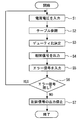
- FIG. 3 is a flowchart illustrating an operation of a control unit according to the first embodiment.
- 6 is a circuit diagram showing a power device driving apparatus according to Embodiment 2.
- FIG. It is a figure which shows the table which concerns on Embodiment 2.
- a power device driving apparatus will be described with reference to the drawings.
- the same or corresponding components are denoted by the same reference numerals, and repeated description may be omitted.
- FIG. 1 is a circuit diagram showing a power device driving apparatus according to the first embodiment.
- the primary coil of the transformer 1 and the switching element 2 are connected in series between the power supply terminal and the ground terminal.
- a capacitor 3 is connected in parallel to the primary coil of the transformer 1.
- the control unit 4 inputs a power supply voltage and generates a control signal.
- the control signal output from the control unit 4 is input to the gate of the switching element 2.
- the switching element 2 switches according to the control signal and generates a primary side input voltage of the transformer 1 from the power supply voltage.
- the transformer 1 converts the primary side input voltage into the secondary side output voltage.
- the capacitor 5 is connected in parallel to the secondary coil of the transformer 1.
- the secondary output voltage of the transformer 1 is input to the drive circuit 7 via the diode 6.
- the drive circuit 7 drives the power device 8 according to the secondary side output voltage.
- the power device 8 is an IGBT or a power MOS transistor.
- An error signal is output from the drive circuit 7 when an abnormality such as a secondary output short circuit occurs. This error signal is input to the control unit 4 on the primary side through an insulating element 9 such as a photocoupler.
- the control unit 4 has a table that summarizes the correspondence between the power supply voltage and the set value of the control signal so that a desired secondary output voltage can be obtained.
- the control signal is a pulse width modulation (Pulse Width Modulation) signal.
- the set value of the control signal is the duty ratio of the pulse width modulation signal.
- FIG. 2 is a diagram illustrating a table according to the first embodiment.
- the control unit 4 generates a control signal having a duty ratio corresponding to the power supply voltage with reference to the table of FIG. Thereby, a desired secondary output voltage can be obtained.
- the control unit 4 is realized by a CPU that executes a program stored in a memory or a processing circuit such as a system LSI. A plurality of processing circuits may cooperate to execute the above function.
- FIG. 3 is a flowchart showing the operation of the control unit according to the first embodiment.
- the control unit 4 inputs a power supply voltage (step S1).
- the control unit 4 refers to the table (step S2), determines the duty ratio of the control signal corresponding to the power supply voltage (step S3), and outputs a control signal having the duty ratio (step S4).
- the controller 4 inputs an error signal transmitted from the secondary side to the primary side every time the duty ratio of the control signal is determined (step S5).
- the control unit 4 determines whether or not there is an error signal (step S6), and stops the output of the control signal when the error signal is transmitted to protect the power device driving device (step S7).
- the setting corresponding to the power supply voltage is referred to by referring to the table that summarizes the correspondence between the power supply voltage and the set value of the control signal so that a desired secondary output voltage can be obtained.
- a control signal having a value is generated, and a primary side input voltage of the transformer 1 is generated from the power supply voltage in accordance with the control signal. This eliminates the need for a peripheral circuit that feeds back the secondary output voltage of the transformer 1, thereby preventing an increase in cost. In addition, since the feedback processing time does not occur, the responsiveness is improved.
- the major fluctuation factors of the secondary side output voltage are the power supply voltage and the driving load of the power device 8.
- the fluctuation range of the power supply voltage is about 8 to 16 V, and there is no sudden fluctuation of the power supply voltage. Therefore, even the control by the table as in this embodiment can cope with the fluctuation of the power supply voltage. Further, by setting the output voltage higher in advance in consideration of the output voltage drop during driving of the power device, it is possible to cope with fluctuations with respect to the power device driving load.
- FIG. FIG. 4 is a circuit diagram showing a power device driving apparatus according to the second embodiment.
- the carrier frequency that is the driving load information of the power device 8 is also input.
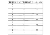
- FIG. 5 is a diagram illustrating a table according to the second embodiment. The table summarizes the power supply voltage, the carrier frequency of the power device, and the duty ratio of the control signal so that a desired secondary output voltage can be obtained.
- the control unit 4 generates a control signal having a duty ratio corresponding to the power supply voltage and the carrier frequency of the power device with reference to the table of FIG. This can cope with output load fluctuations. Other configurations and effects are the same as those of the first embodiment.
- Embodiments 1 and 2 are set based on the experimental results. However, in the inspection process when manufacturing the power device, the secondary output voltage is monitored while changing the power supply voltage input to the control unit 4, and the table is set so that the secondary output voltage becomes a desired voltage. May be. Thereby, the characteristic variation of a structural member can be canceled and a more accurate power supply device can be realized.
- the power device 8 is not limited to being formed of silicon, and may be formed of a wide band gap semiconductor having a larger band gap than silicon.
- the wide band gap semiconductor is, for example, silicon carbide, a gallium nitride-based material, or diamond. Since the power device 8 formed of such a wide band gap semiconductor has high withstand voltage and allowable current density, it can be miniaturized. By using the miniaturized power device 8, a semiconductor module incorporating the power device 8 can be miniaturized. Moreover, since the heat resistance of the power device 8 is high, the heat dissipating fins of the heat sink can be reduced in size, and the water cooling part can be cooled in the air, so that the semiconductor module can be further reduced in size. In addition, since the power device 8 has low power loss and high efficiency, the semiconductor module can be highly efficient.
Landscapes
- Engineering & Computer Science (AREA)
- Power Engineering (AREA)
- Dc-Dc Converters (AREA)
Abstract
制御部(4)が制御信号を生成する。スイッチング素子(2)が制御信号に応じてスイッチングして電源電圧から1次側入力電圧を生成する。トランス(1)が1次側入力電圧を2次側出力電圧に変換する。駆動回路(7)が2次側出力電圧に応じてパワーデバイス(8)を駆動する。制御部(4)は、所望の2次側出力電圧が得られるような電源電圧と制御信号の設定値の対応関係をまとめたテーブルを有し、テーブルを参照して電源電圧に対応する設定値を持った制御信号を生成する。
Description
本発明は、パワーデバイス駆動装置及びその製造方法に関する。
パワーデバイスに対して高機能化・高精度化・高密度化が要求されている。パワーデバイスと制御基板が一体となったIPMにおいても、パワーデバイスの高密度化に伴い、制御基板の更なる高密度化が必要となっている。制御基板の高密度化の手段として、ディスクリート部品をASIC又はマイコンに取り込む集約化が挙げられる。専用の電源用ICをマイコンに取り込んで集約化してデジタル電源化することで電源装置の集約化・高機能化を図る手段がある(例えば、特許文献1参照)。
従来の絶縁型のデジタル電源装置では、2次側出力電圧をフィードバックするためにフォトカプラ又はトランス補助巻線を用いていた。このような周辺回路が必要となるため、コストが増加するという問題があった。
本発明は、上述のような課題を解決するためになされたもので、その目的はコストの増加を防ぐことができるパワーデバイス駆動装置及びその製造方法を得るものである。
本発明に係るパワーデバイス駆動装置は、制御信号を生成する制御部と、前記制御信号に応じてスイッチングして電源電圧から1次側入力電圧を生成するスイッチング素子と、前記1次側入力電圧を2次側出力電圧に変換するトランスと、前記2次側出力電圧に応じてパワーデバイスを駆動する駆動回路とを備え、前記制御部は、所望の2次側出力電圧が得られるような電源電圧と制御信号の設定値の対応関係をまとめたテーブルを有し、前記テーブルを参照して前記電源電圧に対応する設定値を持った前記制御信号を生成することを特徴とする。
本発明では、所望の2次側出力電圧が得られるような電源電圧と制御信号の設定値の対応関係をまとめたテーブルを参照して、電源電圧に対応する設定値を持った制御信号を生成し、この制御信号に応じて電源電圧からトランスの1次側入力電圧を生成する。これにより、トランスの2次側出力電圧をフィードバックする周辺回路が不要となるため、コストの増加を防ぐことができる。
実施の形態に係るパワーデバイス駆動装置について図面を参照して説明する。同じ又は対応する構成要素には同じ符号を付し、説明の繰り返しを省略する場合がある。
実施の形態1.
図1は、実施の形態1に係るパワーデバイス駆動装置を示す回路図である。電源端子と接地端子の間にトランス1の1次側コイルとスイッチング素子2が直列に接続されている。コンデンサ3がトランス1の1次側コイルに並列に接続されている。
図1は、実施の形態1に係るパワーデバイス駆動装置を示す回路図である。電源端子と接地端子の間にトランス1の1次側コイルとスイッチング素子2が直列に接続されている。コンデンサ3がトランス1の1次側コイルに並列に接続されている。
制御部4は、電源電圧を入力して制御信号を生成する。制御部4が出力した制御信号はスイッチング素子2のゲートに入力される。スイッチング素子2は制御信号に応じてスイッチングして電源電圧からトランス1の1次側入力電圧を生成する。トランス1は1次側入力電圧を2次側出力電圧に変換する。
コンデンサ5がトランス1の2次側コイルに並列に接続されている。トランス1の2次側出力電圧はダイオード6を介して駆動回路7に入力される。駆動回路7は2次側出力電圧に応じてパワーデバイス8を駆動する。パワーデバイス8はIGBT又はパワーMOSトランジスタ等である。2次側出力短絡等の異常時に駆動回路7からエラー信号が出力される。このエラー信号は、フォトカプラ等の絶縁素子9を介して1次側の制御部4に入力される。
制御部4は、所望の2次側出力電圧が得られるような電源電圧と制御信号の設定値の対応関係をまとめたテーブルを有する。制御信号はパルス幅変調(Pulse Width Modulation)信号である。制御信号の設定値はパルス幅変調信号のデューティ比である。図2は、実施の形態1に係るテーブルを示す図である。制御部4は、図2のテーブルを参照して電源電圧に対応するデューティ比を持った制御信号を生成する。これにより、所望の2次側出力電圧を得ることができる。なお、制御部4は、メモリに記憶されたプログラムを実行するCPU、又はシステムLSI等の処理回路により実現される。また、複数の処理回路が連携して上記の機能を実行してもよい。
図3は、実施の形態1に係る制御部の動作を示すフローチャートである。まず、制御部4は電源電圧を入力する(ステップS1)。次に、制御部4はテーブルを参照し(ステップS2)、電源電圧に対応する制御信号のデューティ比を決定し(ステップS3)、そのデューティ比を持つ制御信号を出力する(ステップS4)。次に、制御部4は、制御信号のデューティ比の決定毎に、2次側から1次側に伝達されているエラー信号を入力する(ステップS5)。制御部4は、エラー信号の有無を判定し(ステップS6)、エラー信号が伝達された異常時に制御信号の出力を停止してパワーデバイス駆動装置を保護する(ステップS7)。
以上説明したように、本実施の形態では、所望の2次側出力電圧が得られるような電源電圧と制御信号の設定値の対応関係をまとめたテーブルを参照して、電源電圧に対応する設定値を持った制御信号を生成し、この制御信号に応じて電源電圧からトランス1の1次側入力電圧を生成する。これにより、トランス1の2次側出力電圧をフィードバックする周辺回路が不要となるため、コストの増加を防ぐことができる。また、フィードバック処理時間が発生しない分、応答性も改善される。
パワーデバイス駆動装置において、2次側出力電圧の大きな変動要因は電源電圧とパワーデバイス8の駆動負荷である。とりわけ車載用駆動電源となると電源電圧の変動幅は8~16V程度であり、電源電圧の急激な変動はない。従って、本実施の形態のようなテーブルによる制御でも、電源電圧の変動にも対応できる。また、パワーデバイス駆動時の出力電圧低下分を考慮し予め高めに出力電圧を設定することで、パワーデバイス駆動負荷に対する変動にも対応できる。
実施の形態2.
図4は、実施の形態2に係るパワーデバイス駆動装置を示す回路図である。実施の形態1では制御部4に電源電圧のみ入力していたが、本実施の形態ではパワーデバイス8の駆動負荷情報であるキャリア周波数も入力する。図5は、実施の形態2に係るテーブルを示す図である。テーブルは、所望の2次側出力電圧が得られるような電源電圧とパワーデバイスのキャリア周波数と制御信号のデューティ比をまとめたものである。制御部4は、図5のテーブルを参照して電源電圧とパワーデバイスのキャリア周波数に対応するディーティ比を持った制御信号を生成する。これにより出力負荷変動にも対応できる。その他の構成及び効果は実施の形態1と同様である。
図4は、実施の形態2に係るパワーデバイス駆動装置を示す回路図である。実施の形態1では制御部4に電源電圧のみ入力していたが、本実施の形態ではパワーデバイス8の駆動負荷情報であるキャリア周波数も入力する。図5は、実施の形態2に係るテーブルを示す図である。テーブルは、所望の2次側出力電圧が得られるような電源電圧とパワーデバイスのキャリア周波数と制御信号のデューティ比をまとめたものである。制御部4は、図5のテーブルを参照して電源電圧とパワーデバイスのキャリア周波数に対応するディーティ比を持った制御信号を生成する。これにより出力負荷変動にも対応できる。その他の構成及び効果は実施の形態1と同様である。
実施の形態1,2のテーブルは実験結果に基づいて設定される。ただし、パワーデバイス装置製造時の検査工程において、制御部4に入力する電源電圧を変化させながら2次側出力電圧をモニタして2次側出力電圧が所望の電圧となるようにテーブルを設定してもよい。これにより、構成部材の特性変動をキャンセルすることができ、より精度の高い電源装置を実現できる。
なお、パワーデバイス8は、珪素によって形成されたものに限らず、珪素に比べてバンドギャップが大きいワイドバンドギャップ半導体によって形成されたものでもよい。ワイドバンドギャップ半導体は、例えば、炭化珪素、窒化ガリウム系材料、又はダイヤモンドである。このようなワイドバンドギャップ半導体によって形成されたパワーデバイス8は、耐電圧性や許容電流密度が高いため、小型化できる。この小型化されたパワーデバイス8を用いることで、このパワーデバイス8を組み込んだ半導体モジュールも小型化できる。また、パワーデバイス8の耐熱性が高いため、ヒートシンクの放熱フィンを小型化でき、水冷部を空冷化できるので、半導体モジュールを更に小型化できる。また、パワーデバイス8の電力損失が低く高効率であるため、半導体モジュールを高効率化できる。
1 トランス、2 スイッチング素子、4 制御部、7 駆動回路、8 パワーデバイス
Claims (5)
- 制御信号を生成する制御部と、
前記制御信号に応じてスイッチングして電源電圧から1次側入力電圧を生成するスイッチング素子と、
前記1次側入力電圧を2次側出力電圧に変換するトランスと、
前記2次側出力電圧に応じてパワーデバイスを駆動する駆動回路とを備え、
前記制御部は、所望の2次側出力電圧が得られるような電源電圧と制御信号の設定値の対応関係をまとめたテーブルを有し、前記テーブルを参照して前記電源電圧に対応する設定値を持った前記制御信号を生成することを特徴とするパワーデバイス駆動装置。 - 前記制御部は前記2次側出力電圧をフィードバックすることなく前記制御信号を生成することを特徴とする請求項1に記載のパワーデバイス駆動装置。
- 前記制御信号はパルス幅変調信号であり、
前記テーブルは、所望の2次側出力電圧が得られるような電源電圧と制御信号のデューティ比の対応関係をまとめたものであることを特徴とする請求項1又は2に記載のパワーデバイス駆動装置。 - 前記テーブルは、所望の2次側出力電圧が得られるような電源電圧とパワーデバイスの駆動負荷情報と制御信号の設定値の対応関係をまとめたものであり、
前記制御部は、前記テーブルを参照して前記電源電圧と前記パワーデバイスの駆動負荷情報に対応する設定値を持った前記制御信号を生成することを特徴とする請求項1~3の何れか1項に記載のパワーデバイス駆動装置。 - 請求項1~4の何れか1項に記載のパワーデバイス駆動装置を製造する方法であって、
前記制御部に入力する前記電源電圧を変化させながら前記2次側出力電圧をモニタして前記2次側出力電圧が所望の電圧となるように前記テーブルを設定することを特徴とするパワーデバイス駆動装置の製造方法。
Priority Applications (5)
| Application Number | Priority Date | Filing Date | Title |
|---|---|---|---|
| JP2020518859A JP6977876B2 (ja) | 2018-05-15 | 2018-05-15 | パワーデバイス駆動装置及びその製造方法 |
| CN201880093310.9A CN112088481B (zh) | 2018-05-15 | 2018-05-15 | 功率器件驱动装置及其制造方法 |
| US16/959,343 US11563380B2 (en) | 2018-05-15 | 2018-05-15 | Power device drive apparatus and method for manufacturing the same |
| DE112018007618.0T DE112018007618T5 (de) | 2018-05-15 | 2018-05-15 | Leistungsvorrichtungstreibergerät und Verfahren zu dessen Herstellung |
| PCT/JP2018/018787 WO2019220544A1 (ja) | 2018-05-15 | 2018-05-15 | パワーデバイス駆動装置及びその製造方法 |
Applications Claiming Priority (1)
| Application Number | Priority Date | Filing Date | Title |
|---|---|---|---|
| PCT/JP2018/018787 WO2019220544A1 (ja) | 2018-05-15 | 2018-05-15 | パワーデバイス駆動装置及びその製造方法 |
Publications (1)
| Publication Number | Publication Date |
|---|---|
| WO2019220544A1 true WO2019220544A1 (ja) | 2019-11-21 |
Family
ID=68539689
Family Applications (1)
| Application Number | Title | Priority Date | Filing Date |
|---|---|---|---|
| PCT/JP2018/018787 Ceased WO2019220544A1 (ja) | 2018-05-15 | 2018-05-15 | パワーデバイス駆動装置及びその製造方法 |
Country Status (5)
| Country | Link |
|---|---|
| US (1) | US11563380B2 (ja) |
| JP (1) | JP6977876B2 (ja) |
| CN (1) | CN112088481B (ja) |
| DE (1) | DE112018007618T5 (ja) |
| WO (1) | WO2019220544A1 (ja) |
Citations (3)
| Publication number | Priority date | Publication date | Assignee | Title |
|---|---|---|---|---|
| JPH11113252A (ja) * | 1997-10-02 | 1999-04-23 | Fujitsu Ltd | スイッチング電源装置 |
| JPH11136938A (ja) * | 1997-10-31 | 1999-05-21 | Fujitsu Denso Ltd | Dc/dcコンバータ |
| WO2015181919A1 (ja) * | 2014-05-28 | 2015-12-03 | 富士電機株式会社 | 充電器 |
Family Cites Families (11)
| Publication number | Priority date | Publication date | Assignee | Title |
|---|---|---|---|---|
| DK3589081T3 (da) | 2004-03-15 | 2024-03-18 | Signify North America Corp | Effektstyringfremgangsmåder og -apparat |
| JPWO2006101135A1 (ja) * | 2005-03-22 | 2008-09-04 | 沖パワーテック株式会社 | スイッチング電源回路 |
| JP2007288979A (ja) * | 2006-04-19 | 2007-11-01 | Toyota Industries Corp | 直流電源装置 |
| DE102006030655A1 (de) * | 2006-04-21 | 2007-10-25 | Tridonicatco Gmbh & Co. Kg | Notlichtgerät zum Betreiben einer Lichtquelle, insbesondere einer LED |
| JP2009195095A (ja) | 2008-02-14 | 2009-08-27 | Matsuda Micronics Corp | 入力電圧アダプティブ方式電源装置 |
| US8847568B2 (en) * | 2008-09-29 | 2014-09-30 | Infineon Technologies Ag | Sample-point adjustment in a switching converter |
| CN101645658B (zh) * | 2009-05-27 | 2013-09-18 | 北京中星微电子有限公司 | 反激式电源转换器及反激式电源转换器的环路控制方法 |
| US8362756B2 (en) * | 2010-12-21 | 2013-01-29 | Exar Corporation | Digital boost feedback voltage controller for switch-mode power supplies using pulse-frequency modulation |
| JP2013046438A (ja) * | 2011-08-22 | 2013-03-04 | Omron Automotive Electronics Co Ltd | Dc−dcコンバータ |
| WO2015022097A1 (de) * | 2013-08-15 | 2015-02-19 | Conti Temic Microelectronic Gmbh | Kennlinienbasierte vorsteuerung von eingangsspannungs- und ausgangsstromänderungen in einem schaltnetzteil |
| CN109995254B (zh) * | 2017-12-29 | 2020-12-29 | 东南大学 | 一种提高同步整流原边反馈反激式电源动态性能的方法 |
-
2018
- 2018-05-15 CN CN201880093310.9A patent/CN112088481B/zh active Active
- 2018-05-15 US US16/959,343 patent/US11563380B2/en active Active
- 2018-05-15 DE DE112018007618.0T patent/DE112018007618T5/de active Pending
- 2018-05-15 WO PCT/JP2018/018787 patent/WO2019220544A1/ja not_active Ceased
- 2018-05-15 JP JP2020518859A patent/JP6977876B2/ja active Active
Patent Citations (3)
| Publication number | Priority date | Publication date | Assignee | Title |
|---|---|---|---|---|
| JPH11113252A (ja) * | 1997-10-02 | 1999-04-23 | Fujitsu Ltd | スイッチング電源装置 |
| JPH11136938A (ja) * | 1997-10-31 | 1999-05-21 | Fujitsu Denso Ltd | Dc/dcコンバータ |
| WO2015181919A1 (ja) * | 2014-05-28 | 2015-12-03 | 富士電機株式会社 | 充電器 |
Also Published As
| Publication number | Publication date |
|---|---|
| DE112018007618T5 (de) | 2021-01-28 |
| JP6977876B2 (ja) | 2021-12-08 |
| US11563380B2 (en) | 2023-01-24 |
| US20200358362A1 (en) | 2020-11-12 |
| CN112088481B (zh) | 2024-06-14 |
| JPWO2019220544A1 (ja) | 2021-02-12 |
| CN112088481A (zh) | 2020-12-15 |
Similar Documents
| Publication | Publication Date | Title |
|---|---|---|
| JP6184137B2 (ja) | 電力管理チップ及びそれを備える電力管理装置 | |
| US11626790B2 (en) | Power conversion device minimizing footprint | |
| US3124697A (en) | Voltage regulating arrangement | |
| JP6977876B2 (ja) | パワーデバイス駆動装置及びその製造方法 | |
| JP6729474B2 (ja) | 半導体装置 | |
| JP2016213659A (ja) | 半導体スイッチ回路 | |
| WO2019054051A1 (ja) | ゲート駆動回路、および、パワースイッチングシステム | |
| JP6504250B2 (ja) | 制御回路 | |
| US10630279B2 (en) | Power semiconductor device | |
| US20160261203A1 (en) | Insulated synchronous rectification dc/dc converter | |
| US20230070322A1 (en) | Semiconductor device | |
| JP5950961B2 (ja) | ゲート駆動回路 | |
| US20210391802A1 (en) | Dc-dc converter | |
| SK1262023A3 (sk) | Zapojenie budiaceho obvodu pre sériové zapojenie tranzistorového modulu | |
| US20130293002A1 (en) | Device comprising an electronic component with high switching speed | |
| CN109983699B (zh) | 栅极驱动电路 | |
| SK10055Y1 (sk) | Zapojenie budiaceho obvodu pre sériové zapojenie tranzistorového modulu | |
| US12512834B2 (en) | Semiconductor device | |
| WO2025204075A1 (ja) | 電源装置 | |
| JPWO2019073506A1 (ja) | 半導体装置、及び、電力変換装置 | |
| CN119447131A (zh) | 异构芯片及设备 | |
| TWM643423U (zh) | 氮化鎵高電子遷移率電晶體開關晶片 | |
| CN121036539A (zh) | 一种单芯片准关断模式dc/dc降压转换器及其转换方法 | |
| JP2024031344A (ja) | 電源装置 | |
| JP2003274661A (ja) | スイッチング電源回路 |
Legal Events
| Date | Code | Title | Description |
|---|---|---|---|
| 121 | Ep: the epo has been informed by wipo that ep was designated in this application |
Ref document number: 18918978 Country of ref document: EP Kind code of ref document: A1 |
|
| ENP | Entry into the national phase |
Ref document number: 2020518859 Country of ref document: JP Kind code of ref document: A |
|
| 122 | Ep: pct application non-entry in european phase |
Ref document number: 18918978 Country of ref document: EP Kind code of ref document: A1 |