WO2019218447A1 - 一种基于记忆二极管的三态内容寻址存储器 - Google Patents
一种基于记忆二极管的三态内容寻址存储器 Download PDFInfo
- Publication number
- WO2019218447A1 WO2019218447A1 PCT/CN2018/095745 CN2018095745W WO2019218447A1 WO 2019218447 A1 WO2019218447 A1 WO 2019218447A1 CN 2018095745 W CN2018095745 W CN 2018095745W WO 2019218447 A1 WO2019218447 A1 WO 2019218447A1
- Authority
- WO
- WIPO (PCT)
- Prior art keywords
- memory
- state
- diode
- memory diode
- kernel
- Prior art date
- Legal status (The legal status is an assumption and is not a legal conclusion. Google has not performed a legal analysis and makes no representation as to the accuracy of the status listed.)
- Ceased
Links
Images


Classifications
-
- H—ELECTRICITY
- H10—SEMICONDUCTOR DEVICES; ELECTRIC SOLID-STATE DEVICES NOT OTHERWISE PROVIDED FOR
- H10N—ELECTRIC SOLID-STATE DEVICES NOT OTHERWISE PROVIDED FOR
- H10N70/00—Solid-state devices having no potential barriers, and specially adapted for rectifying, amplifying, oscillating or switching
- H10N70/20—Multistable switching devices, e.g. memristors
-
- G—PHYSICS
- G11—INFORMATION STORAGE
- G11C—STATIC STORES
- G11C15/00—Digital stores in which information comprising one or more characteristic parts is written into the store and in which information is read-out by searching for one or more of these characteristic parts, i.e. associative or content-addressed stores
- G11C15/04—Digital stores in which information comprising one or more characteristic parts is written into the store and in which information is read-out by searching for one or more of these characteristic parts, i.e. associative or content-addressed stores using semiconductor elements
- G11C15/046—Digital stores in which information comprising one or more characteristic parts is written into the store and in which information is read-out by searching for one or more of these characteristic parts, i.e. associative or content-addressed stores using semiconductor elements using non-volatile storage elements
-
- G—PHYSICS
- G11—INFORMATION STORAGE
- G11C—STATIC STORES
- G11C15/00—Digital stores in which information comprising one or more characteristic parts is written into the store and in which information is read-out by searching for one or more of these characteristic parts, i.e. associative or content-addressed stores
- G11C15/04—Digital stores in which information comprising one or more characteristic parts is written into the store and in which information is read-out by searching for one or more of these characteristic parts, i.e. associative or content-addressed stores using semiconductor elements
-
- H—ELECTRICITY
- H10—SEMICONDUCTOR DEVICES; ELECTRIC SOLID-STATE DEVICES NOT OTHERWISE PROVIDED FOR
- H10N—ELECTRIC SOLID-STATE DEVICES NOT OTHERWISE PROVIDED FOR
- H10N70/00—Solid-state devices having no potential barriers, and specially adapted for rectifying, amplifying, oscillating or switching
- H10N70/011—Manufacture or treatment of multistable switching devices
- H10N70/061—Shaping switching materials
- H10N70/066—Shaping switching materials by filling of openings, e.g. damascene method
-
- H—ELECTRICITY
- H10—SEMICONDUCTOR DEVICES; ELECTRIC SOLID-STATE DEVICES NOT OTHERWISE PROVIDED FOR
- H10N—ELECTRIC SOLID-STATE DEVICES NOT OTHERWISE PROVIDED FOR
- H10N70/00—Solid-state devices having no potential barriers, and specially adapted for rectifying, amplifying, oscillating or switching
- H10N70/801—Constructional details of multistable switching devices
- H10N70/821—Device geometry
- H10N70/826—Device geometry adapted for essentially vertical current flow, e.g. sandwich or pillar type devices
-
- H—ELECTRICITY
- H10—SEMICONDUCTOR DEVICES; ELECTRIC SOLID-STATE DEVICES NOT OTHERWISE PROVIDED FOR
- H10N—ELECTRIC SOLID-STATE DEVICES NOT OTHERWISE PROVIDED FOR
- H10N70/00—Solid-state devices having no potential barriers, and specially adapted for rectifying, amplifying, oscillating or switching
- H10N70/801—Constructional details of multistable switching devices
- H10N70/881—Switching materials
- H10N70/883—Oxides or nitrides
- H10N70/8833—Binary metal oxides, e.g. TaOx
Definitions
- the invention belongs to the field of semiconductors and integrated circuits, and in particular relates to a high-density, low-power tristate content addressable memory based on a memory diode.
- TCAM Ternary Content Addressable Memory
- MRAM magnetic memory
- PCM phase change memory
- the object of the present invention is to provide a tri-state content-addressable memory based on a memory diode, which reduces the chip size and reduces power consumption, and is compatible with a standard CMOS process, in view of the deficiencies of the existing three-state content addressable memory.
- a memory diode which is sequentially stacked from bottom to top by a bottom electrode, an isolation layer, a memory layer and a top electrode;
- the memory layer is made of yttrium oxide and oxidized Aluminum and yttrium oxide are stacked in order from bottom to top;
- the material of the bottom electrode is ruthenium.
- the material of the isolation layer includes, but is not limited to, silicon oxide;
- the top electrode may be formed by stacking titanium nitride and nickel metal.
- the memory diode has its bottom electrode grounded, and a corresponding voltage is applied to its top electrode, thereby realizing the conversion of the memory diode between the off state and the on state.
- the memory diode in the off state suddenly decreases in resistance after applying the negative voltage.
- This process is called SET, and the memory diode is turned from the off state to the on state, which can be regarded as a diode device; the memory diode in the on state is applied. After the forward voltage, the resistance suddenly increases. This process is called RESET.
- RESET The memory diode turns from the on state to the off state, which can be regarded as a resistor with high resistance.
- a memory diode-based three-state content addressable memory comprising a plurality of core units having the functions of storing data, erasing data and comparing data;
- the kernel units are arranged in an array, and all kernel units in units of rows are connected to the same matching line, and all kernel units in column units are connected to the same pair of complementary search signal lines;
- the core unit includes a first memory diode and a second memory diode; the top electrodes of the first memory diode and the second memory diode are respectively connected to a pair of complementary search signal lines, and the bottom electrodes of the first memory diode and the second memory diode Connect the same match line.
- the matching line material is ⁇ , and is used for generating a voltage signal after the search signal is compared with the stored data;
- the search signal line is a metal line connected to the top electrode of the diode, for inputting the search signal and for the memory A signal that is stored in the diode for erasing data.
- the first memory diode and the second memory diode in the core unit cooperate to store three logic states of [0], [1], and [don't care]: when the first memory diode When the second memory diode is in the off state, the core unit stores the data bit [0]; when the first memory diode is in the off state and the second memory diode is in the on state, the core unit stores the data bit [1] When the first memory diode and the second memory diode are both in an off state, the core unit is in a [don't care] state.
- the kernel unit when the kernel unit stores the data bits in accordance with the search signal, it is a match.
- the match line When all kernel units on the same match line are in a match state, the match line outputs [0]; when the kernel When the unit storage data bit is inconsistent with the search signal, it is a mismatch. When one or more core units on the same match line are mismatched, the match line outputs [1].
- the present invention can greatly reduce the size of the tri-state content addressed memory chip.
- the present invention can reduce power consumption.
- the present invention has a simple structure, which simplifies the preparation process and reduces the manufacturing cost.
- the present invention is compatible with standard CMOS processes and is suitable for currently rapidly developing semiconductor integrated circuits.
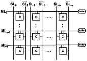
- FIG. 1 is a schematic structural diagram of a tri-state content addressing memory based on a memory diode according to the present invention
- FIG. 2 is a schematic structural view of a memory diode according to the present invention.
- FIG. 3 is a current-voltage characteristic diagram of a memory diode in the present invention.
- FIG. 4 is a circuit diagram of a core unit in the present invention.
- FIG. 5 is a schematic diagram of four data matching result circuits obtained according to an embodiment of the present invention.
- Figure 6 is a result of matching obtained in accordance with an embodiment of the present invention.
- FIG. 1 is a schematic structural diagram of a three-state content addressable memory based on a memory diode according to the present invention.
- the tri-state content addressable memory includes a plurality of core units (C) having functions of storing data, erasing data, and comparing data; the core units (C) are arranged in an array, and all kernel units in units of rows are connected to the same matching line. (ML), all kernel units in columns are connected to the same pair of complementary search signal lines A total of m bits are stored on the same match line (ML), and each search signal contains m bits.
- the n match lines indicate that the three-state content addressed memory stores a total of n words.
- the memory diode is formed by sequentially stacking a bottom electrode, an isolation layer, a memory layer and a top electrode from bottom to top; the memory layer is formed by stacking yttrium oxide, aluminum oxide and yttrium oxide from bottom to top; the material of the bottom electrode Why?
- the material of the isolation layer includes, but is not limited to, silicon oxide; the top electrode may be formed by stacking titanium nitride and nickel metal.
- a preparation method of the memory diode is given below, including the following steps:
- Figure 3 is a graph showing current-voltage characteristics of a memory diode in accordance with the present invention.
- the memory diode In the working state, the memory diode has its bottom electrode grounded, and a corresponding voltage is applied to the top electrode, thereby realizing the conversion between the memory diode in the off state (I, IV state in the figure) and the on state (II, III state in the figure).
- the memory diode in the off state suddenly decreases in resistance after applying a negative voltage.
- This process is called SET, and the memory diode is turned from the off state to the on state, which can be regarded as a diode device; the memory diode in the on state is After the forward voltage is applied, the resistance suddenly increases.
- RESET RESET.
- the memory diode turns from the on state to the off state, which can be regarded as a resistor with a high resistance value.
- the current of the III state is more than 2 times larger than the current of the II state; and when the same read voltage is applied to the open and closed memory diodes respectively, The state current is more than 2 times larger than the off-state current.
- Each core unit includes a first memory diode and a second memory diode.
- the top electrodes of the first memory diode and the second memory diode are respectively connected to a pair of complementary search signal lines, and the bottom electrodes of the first memory diode and the second memory diode are connected to the same matching line.
- the material of the matching line is ⁇
- the search signal line is a metal line connected to the top electrode of the diode.
- FIG. 5 is a schematic diagram of four data matching result circuits obtained according to an embodiment of the present invention.
- the first memory diode and the second memory diode in the core unit cooperate to store three logic states [0], [1], and [don't care]: when the first memory diode is in an on state, When the memory diode is in the off state, the core unit stores the data bit [0]; when the first memory diode is in the off state and the second memory diode is in the on state, the core unit stores the data bit [1]; when the first memory When the diode and the second memory diode are both off, the core unit is in a [don't care] state.
- the match line When the kernel unit stores the data bits in accordance with the search signal, it is a match. When all kernel units on the same match line are in a match state, the match line outputs [0]; when the kernel unit stores data When the bit is inconsistent with the search signal, it is a mismatch. When one or more core units on the same match line are mismatched, the match line outputs [1].
- the 101 core unit is in a mismatch state, the core unit stores the data bit [0], the search signal is [1], and the current flows smoothly through the open state memory diode in the core unit, so that the matching line (ML 0 The voltage rises, the output [1]; the 102 core unit is in a match state, the core unit stores the data bit [0], and the seek signal is [0].
- the open state memory diode in the core unit has a diode characteristic, The mismatch current caused by the 101 core unit does not flow from the open state memory diode, thereby maintaining the voltage of the same match line (ML 0 ); the 103 core unit is in a match state, and the core unit stores the data bit [1], The search signal is [1], which does not affect the match line (ML 1 ) voltage; the 104 core unit is in a match state, the kernel unit stores [don't care], and the search signal is [1], which does not affect Match line (ML 1 ) voltage, output [0].
- Figure 6 is a result of matching obtained in accordance with an embodiment of the present invention.
- the three-state content addressing memory stores a total of eight words, which are represented by hexadecimal numbers as FF, 00, A5, 5A, AX, X5, FX, and X0, respectively.
- the lookup signal is expressed in hexadecimal as FF. It can be seen from the table that when the search signal and the stored data match each other, the output voltage on the corresponding matching line is very low, and when the search signal and the stored data are mismatched, the output voltage on the corresponding matching line is relatively high.
Landscapes
- Engineering & Computer Science (AREA)
- Manufacturing & Machinery (AREA)
- Semiconductor Memories (AREA)
Abstract
本发明公开了一种基于记忆二极管的三态内容寻址存储器,包括若干兼具存储数据、擦写数据和比较数据功能的内核单元;内核单元呈阵列排列,以行为单位的所有内核单元连接同一匹配线,以列为单位的所有内核单元连接同一对互补搜寻信号线;内核单元包括两个记忆二极管;第一记忆二极管和第二记忆二极管的顶电极分别接一对互补搜寻信号线,第一记忆二极管和第二记忆二极管的底电极连接同一匹配线。本发明可以大大缩小三态内容寻址存储器芯片尺寸,减小功耗;本发明三态内容寻址存储器结构简单,有效简化制备工艺并且降低制备成本;本发明提出并实现了与标准CMOS工艺兼容性的记忆二极管,适合于当前快速发展的集成电路技术。
Description
本发明属于半导体与集成电路领域,具体涉及一种基于记忆二极管的高密度、低功耗三态内容寻址存储器。
三态内容寻址存储器(Ternary Content Addressable memory,TCAM)具有并行多数据查找的功能,应用范围广泛,如参数曲线提取(parameter curve extraction)、霍夫变换(Hough transformation)、霍夫曼编码/译码(Huffman coding/decoding)等,主要的商业用途是在网络路由器中对IP数据包进行分类和转发。
当前对三态内容寻址存储器的设计中大家最关注的是芯片尺寸和功耗问题。虽然目前基于磁性存储器(MRAM)、相变存储器(PCM)的非易失内容存储器单元已经实现,但是其结构复杂,且制备工艺与标准CMOS工艺并不能完全兼容。
发明内容
本发明的目的在于针对现有三态内容寻址存储器的不足,提供一种基于记忆二极管的三态内容寻址存储器,减小芯片尺寸,降低功耗,与标准CMOS工艺良好兼容。
本发明的目的是通过以下技术方案来实现的:一种记忆二极管,该记忆二极管由底电极、隔离层、记忆层、顶电极从下至上依次堆叠而成;所述记忆层由氧化锗、氧化铝、氧化铪从下至上依次堆叠而成;所述底电极的材料为锗。所述隔离层的材料包括但不限于氧化硅;所述顶电极可以由氮化钛和金属镍堆叠而成。
进一步地,记忆二极管在工作状态中其底电极接地,在其顶电极施加相应电压,从而实现记忆二极管在关态与开态之间的转化。
进一步地,处于关态的记忆二极管在施加负向电压后电阻突然减小,这个过程称为SET,记忆二极管由关态转为开态,可视作二极管器件;处于开态的记忆二极管在施加正向电压后电阻突然增大,这个过程称为RESET,记忆二极管由开态转为关态,可视作具有高阻值的电阻。
一种基于记忆二极管的三态内容寻址存储器,该三态内容寻址存储器包括若干兼具存储数据、擦写数据和比较数据功能的内核单元;
所述内核单元呈阵列排列,以行为单位的所有内核单元连接同一匹配线,以列为单位的所有内核单元连接同一对互补搜寻信号线;
所述内核单元包括第一记忆二极管和第二记忆二极管;所述第一记忆二极管和第二记忆二极管的顶电极分别接一对互补搜寻信号线,第一记忆二极管和第二记忆二极管的底电极连接同一匹配线。
进一步地,所述匹配线材料为锗,用于产生搜寻信号与存储数据进行比较后的电压信号;所述搜寻信号线为与二极管的顶电极连接的金属线,用于输入搜寻信号以及对记忆二极管内存储数据进行擦写的信号。
进一步地,所述内核单元中的第一记忆二极管和第二记忆二极管相互配合以存储[0]、[1]及[不理会(don’t care)]三种逻辑状态:当第一记忆二极管处于开态,第二记忆二极管处于关态时,该内核单元存储数据位[0];当第一记忆二极管处于关态,第二记忆二极管处于开态时,该内核单元存储数据位[1];当第一记忆二极管和第二记忆二极管都处于关态时,该内核单元为[不理会(don’t care)]状态。
进一步地,当内核单元存储数据位与搜寻信号一致时,为匹配状态(match),当同一条匹配线上的所有内核单元均为匹配状态(match)时,匹配线输出[0];当内核单元存储数据位与搜寻信号不一致时,为失配状态(mismatch),当同一条匹配线上具有一个及以上的内核单元为失配状态(mismatch)时,匹配线输出[1]。
本发明的有益技术效果是:第一,本发明可以大大缩小三态内容寻址存储器芯片尺寸。第二,本发明可以减小功耗。第三,本发明结构简单,有效简化制备工艺并且降低制备成本。第四,本发明与标准CMOS工艺兼容性良好,适合当前快速发展的半导体集成电路。
图1为本发明基于记忆二极管的三态内容寻址存储器的结构示意图;
图2为本发明中记忆二极管的结构示意图;
图3为本发明中记忆二极管的电流-电压特性图;
图4为本发明中内核单元的电路示意图;
图5为按照本发明实施例所得的四种数据匹配结果电路示意图;
图6为按照本发明实施例所得的匹配结果。
下面介绍的是本发明的多个可能实施例中的一些,旨在提供对本发明的基本了解,并不旨在确认本发明的关键或决定性的要素或限定所要保护的范围。容易理解,根据本发明的技术方案,在不变更本发明的实质精神下,本领域的一般技术人员可以提出可相互替换的其他实现方式。因此,以下具体实施方式以及附图仅是对本发明的技术方案的示例性说明,而不应当视为本发明的全部或者是为对本发明技术方案的限定或限制。
图1为本发明基于记忆二极管的三态内容寻址存储器的结构示意图。该三态内容寻址存储器包括若干兼具存储数据、擦写数据和比较数据功能的内核单元(C);所述内核单元(C)呈阵列排列,以行为单位的所有内核单元连接同一匹配线(ML),以列为单位的所有内核单元连接同一对互补搜寻信号线
 同一条匹配线(ML)上共存储m个比特位,每一查找信号中包含m个比特位。n条匹配线表示此三态内容寻址存储器共存储n个字。
图2为本发明中记忆二极管的结构示意图。该记忆二极管由底电极、隔离层、记忆层、顶电极从下至上依次堆叠而成;所述记忆层由氧化锗、氧化铝、氧化铪从下至上依次堆叠而成;所述底电极的材料为锗。所述隔离层的材料包括但不限于氧化硅;所述顶电极可以由氮化钛和金属镍堆叠而成。以下给出记忆二极管的一种制备方法,包括以下步骤:
a)提供一锗衬底,于所述锗衬底表面形成隔离层;
b)在形成的隔离层上进行光刻,并通过化学湿法刻蚀方法刻蚀,直至锗衬底的上表面;
c)于所述刻蚀后的锗衬底上形成记忆层氧化锗/氧化铝/氧化铪结构;
d)于所述记忆层上形成顶电极氮化钛/镍。
图3为按照本发明中记忆二极管的电流-电压特性图。该记忆二极管在工作状态中其底电极接地,在其顶电极施加相应电压,从而实现记忆二极管在关态(图中Ⅰ、Ⅳ状态)与开态(图中Ⅱ、Ⅲ状态)之间的转化,具体为:处于关态的记忆二极管在施加负向电压后电阻突然减小,这个过程称为SET,记忆二极管由关态转为开态,可视作二极管器件;处于开态的记忆二极管在施加正向电压后电阻突然增大,这个过程称为RESET,记忆二极管由开态转为关态,可视作具有高阻值的电阻。
在处于开态的记忆二极管上施加幅值相同的读电压时,Ⅲ状态的电流比Ⅱ状态的电流大2倍以上;而分别在开态与关态的记忆二极管上施加相同读电压时, 开态电流比关态电流大2倍以上。
图4为本发明中内核单元的电路示意图。每个内核单元包括第一记忆二极管和第二记忆二极管。第一记忆二极管和第二记忆二极管的顶电极分别接一对互补搜寻信号线,第一记忆二极管和第二记忆二极管的底电极连接同一匹配线。所述匹配线的材料为锗,所述搜寻信号线为与二极管的顶电极连接的金属线。
图5为按照本发明实施例所得的四种数据匹配结果电路示意图。内核单元中的第一记忆二极管和第二记忆二极管相互配合以存储[0]、[1]及[不理会(don’t care)]三种逻辑状态:当第一记忆二极管处于开态,第二记忆二极管处于关态时,该内核单元存储数据位[0];当第一记忆二极管处于关态,第二记忆二极管处于开态时,该内核单元存储数据位[1];当第一记忆二极管和第二记忆二极管都处于关态时,该内核单元为[不理会(don’t care)]状态。
当内核单元存储数据位与搜寻信号一致时,为匹配状态(match),当同一条匹配线上的所有内核单元均为匹配状态(match)时,匹配线输出[0];当内核单元存储数据位与搜寻信号不一致时,为失配状态(mismatch),当同一条匹配线上具有一个及以上的内核单元为失配状态(mismatch)时,匹配线输出[1]。
如图5,101内核单元处于失配状态(mismatch),内核单元存储数据位[0],搜寻信号为[1],电流顺利流经内核单元内的开态记忆二极管,使得匹配线(ML
0)的电压升高,输出[1];102内核单元处于匹配状态(match),内核单元存储数据位[0],搜寻信号为[0],由于该内核单元中开态记忆二极管具有二极管特性,101内核单元造成的失配电流并不能从此开态记忆二极管流过,从而保持同一匹配线(ML
0)的电压;103内核单元处于匹配状态(match),内核单元存储数据位[1],搜寻信号为[1],不影响匹配线(ML
1)电压;104内核单元处于匹配状态(match),内核单元存储[不理会(don’t care)],搜寻信号为[1],不影响匹配线(ML
1)电压,输出[0]。
图6为按照本发明实施例所得的匹配结果。此实施例中三态内容寻址存储器共存储了8个字,以十六进制分别表示为FF、00、A5、5A、AX、X5、FX、X0。查找信号以十六进制表示为FF。由此表可看出,当查找信号与存储数据相互匹配时,相应匹配线上输出电压很低,而当查找信号与存储数据失配时,相应匹配线上输出电压相对很高。
Claims (7)
- 一种记忆二极管,其特征在于,该记忆二极管由底电极、隔离层、记忆层、顶电极从下至上依次堆叠而成;所述记忆层由氧化锗、氧化铝、氧化铪从下至上依次堆叠而成;所述底电极的材料为锗。
- 根据权利要求1所述的记忆二极管,其特征在于,记忆二极管在工作状态中其底电极接地,在其顶电极施加相应电压,从而实现记忆二极管在关态与开态之间的转化。
- 根据权利要求2所述的记忆二极管,其特征在于,处于关态的记忆二极管在施加负向电压后电阻突然减小,这个过程称为SET,记忆二极管由关态转为开态,可视作二极管器件;处于开态的记忆二极管在施加正向电压后电阻突然增大,这个过程称为RESET,记忆二极管由开态转为关态,可视作具有高阻值的电阻。
- 一种基于记忆二极管的三态内容寻址存储器,其特征在于,该三态内容寻址存储器包括若干兼具存储数据、擦写数据和比较数据功能的内核单元;所述内核单元呈阵列排列,以行为单位的所有内核单元连接同一匹配线,以列为单位的所有内核单元连接同一对互补搜寻信号线;所述内核单元包括第一记忆二极管和第二记忆二极管;所述第一记忆二极管和第二记忆二极管的顶电极分别接一对互补搜寻信号线,第一记忆二极管和第二记忆二极管的底电极连接同一匹配线。
- 根据权利要求4所述的基于记忆二极管的三态内容寻址存储器,其特征在于,所述匹配线的材料为锗,所述搜寻信号线为与记忆二极管的顶电极连接的金属线。
- 根据权利要求4所述的基于记忆二极管的三态内容寻址存储器,其特征在于,所述内核单元中的第一记忆二极管和第二记忆二极管相互配合以存储[0]、[1]及[不理会(don’t care)]三种逻辑状态:当第一记忆二极管处于开态,第二记忆二极管处于关态时,该内核单元存储数据位[0];当第一记忆二极管处于关态,第二记忆二极管处于开态时,该内核单元存储数据位[1];当第一记忆二极管和第二记忆二极管都处于关态时,该内核单元为[不理会(don’t care)]状态。
- 根据权利要求6所述的基于记忆二极管的三态内容寻址存储器,其特征在于,当内核单元存储数据位与搜寻信号一致时,为匹配状态(match),当同一条匹配线上的所有内核单元均为匹配状态(match)时,匹配线输出[0];当内 核单元存储数据位与搜寻信号不一致时,为失配状态(mismatch),当同一条匹配线上具有一个及以上的内核单元为失配状态(mismatch)时,匹配线输出[1]。
Priority Applications (3)
| Application Number | Priority Date | Filing Date | Title |
|---|---|---|---|
| JP2019538661A JP6751478B2 (ja) | 2018-05-14 | 2018-07-16 | メモリダイオードに基づく三値連想メモリ |
| US17/049,585 US11328774B2 (en) | 2018-05-14 | 2018-07-16 | Ternary content addressable memory based on memory diode |
| US17/704,041 US11848052B2 (en) | 2018-05-14 | 2022-03-25 | Ternary content addressable memory based on memory diode |
Applications Claiming Priority (2)
| Application Number | Priority Date | Filing Date | Title |
|---|---|---|---|
| CN201810458536.6A CN108615812B (zh) | 2018-05-14 | 2018-05-14 | 一种基于记忆二极管的三态内容寻址存储器 |
| CN201810458536.6 | 2018-05-14 |
Related Child Applications (2)
| Application Number | Title | Priority Date | Filing Date |
|---|---|---|---|
| US17/049,585 A-371-Of-International US11328774B2 (en) | 2018-05-14 | 2018-07-16 | Ternary content addressable memory based on memory diode |
| US17/704,041 Division US11848052B2 (en) | 2018-05-14 | 2022-03-25 | Ternary content addressable memory based on memory diode |
Publications (1)
| Publication Number | Publication Date |
|---|---|
| WO2019218447A1 true WO2019218447A1 (zh) | 2019-11-21 |
Family
ID=63663179
Family Applications (1)
| Application Number | Title | Priority Date | Filing Date |
|---|---|---|---|
| PCT/CN2018/095745 Ceased WO2019218447A1 (zh) | 2018-05-14 | 2018-07-16 | 一种基于记忆二极管的三态内容寻址存储器 |
Country Status (4)
| Country | Link |
|---|---|
| US (2) | US11328774B2 (zh) |
| JP (1) | JP6751478B2 (zh) |
| CN (1) | CN108615812B (zh) |
| WO (1) | WO2019218447A1 (zh) |
Families Citing this family (4)
| Publication number | Priority date | Publication date | Assignee | Title |
|---|---|---|---|---|
| US11379279B2 (en) * | 2018-06-28 | 2022-07-05 | Juniper Networks, Inc. | Netlink asynchronous notifications for native and third party application in distributed network systems |
| CN111210860B (zh) * | 2019-12-31 | 2022-03-18 | 浙江大学 | 一种基于3d mos器件的三态内容可寻址存储器 |
| US12112792B2 (en) * | 2021-08-10 | 2024-10-08 | Micron Technology, Inc. | Memory device for wafer-on-wafer formed memory and logic |
| CN116913340B (zh) * | 2023-08-08 | 2025-10-14 | 浙江大学 | 一种或非逻辑式的存内逻辑计算系统及计算方法 |
Citations (5)
| Publication number | Priority date | Publication date | Assignee | Title |
|---|---|---|---|---|
| CN104752608A (zh) * | 2013-12-26 | 2015-07-01 | 北京有色金属研究总院 | 一种忆阻器及其制备方法 |
| CN106206944A (zh) * | 2016-09-29 | 2016-12-07 | 南京大学 | 一种纳米薄膜忆阻器及其制备方法 |
| CN106654009A (zh) * | 2016-12-19 | 2017-05-10 | 中国科学院宁波材料技术与工程研究所 | 一种忆阻器及其应用 |
| US9847132B1 (en) * | 2016-07-28 | 2017-12-19 | Hewlett Packard Enterprise Development Lp | Ternary content addressable memories |
| CN107945830A (zh) * | 2016-10-12 | 2018-04-20 | 复旦大学 | 一种非易失三态内容寻址存储器及其寻址方法 |
Family Cites Families (20)
| Publication number | Priority date | Publication date | Assignee | Title |
|---|---|---|---|---|
| US6879532B1 (en) * | 2002-04-10 | 2005-04-12 | Integrated Device Technology, Inc. | Content addressable and random access memory devices having high-speed sense amplifiers therein with low power consumption requirements |
| US7379317B2 (en) * | 2004-12-23 | 2008-05-27 | Spansion Llc | Method of programming, reading and erasing memory-diode in a memory-diode array |
| US7450416B1 (en) * | 2004-12-23 | 2008-11-11 | Spansion Llc | Utilization of memory-diode which may have each of a plurality of different memory states |
| CN101887748A (zh) * | 2009-05-13 | 2010-11-17 | 苏州全芯科技有限公司 | 一种带影子非挥发存储器的cam/tcam |
| US8274065B2 (en) * | 2009-10-19 | 2012-09-25 | Macronix International Co., Ltd. | Memory and method of fabricating the same |
| JP5186634B2 (ja) | 2010-06-29 | 2013-04-17 | シャープ株式会社 | 不揮発性半導体記憶装置 |
| CN102610748B (zh) * | 2011-01-25 | 2014-02-12 | 中国科学院微电子研究所 | 非挥发性存储单元及存储器 |
| TWI570891B (zh) * | 2011-05-17 | 2017-02-11 | 半導體能源研究所股份有限公司 | 半導體裝置 |
| US8908407B1 (en) * | 2011-07-30 | 2014-12-09 | Rambus Inc. | Content addressable memory (“CAM”) |
| US8791444B2 (en) * | 2011-11-23 | 2014-07-29 | National Chiao Tung University | Resistive random access memory (RRAM) using stacked dielectrics and method for manufacturing the same |
| JP2013157469A (ja) * | 2012-01-30 | 2013-08-15 | Sharp Corp | 可変抵抗素子、及び、不揮発性半導体記憶装置 |
| EP2626861B1 (en) * | 2012-02-13 | 2015-01-07 | Crocus Technology S.A. | High speed magnetic random access memory-based ternary CAM |
| JP6179818B2 (ja) * | 2012-09-06 | 2017-08-16 | 日本電気株式会社 | 不揮発性連想メモリ |
| JP6044931B2 (ja) * | 2012-12-11 | 2016-12-14 | 国立大学法人東京農工大学 | 半導体メモリ装置およびその製造方法 |
| JP2015018591A (ja) * | 2013-07-12 | 2015-01-29 | 株式会社東芝 | 不揮発性半導体記憶装置 |
| JP6261041B2 (ja) * | 2014-03-25 | 2018-01-17 | 国立大学法人東北大学 | 不揮発性連想メモリセル及び不揮発性連想メモリ |
| US9306160B2 (en) * | 2014-06-19 | 2016-04-05 | Macronix International Co., Ltd. | Memory device having oxygen control layers and manufacturing method of same |
| WO2016007035A1 (en) * | 2014-07-07 | 2016-01-14 | Nokia Technologies Oy | Sensing device and method of production thereof |
| CN107919155A (zh) * | 2016-10-11 | 2018-04-17 | 复旦大学 | 一种非易失三态内容寻址存储器及其寻址方法 |
| US10453862B1 (en) * | 2018-03-28 | 2019-10-22 | Sandisk Technologies Llc | Ferroelectric non-volatile memory |
-
2018
- 2018-05-14 CN CN201810458536.6A patent/CN108615812B/zh active Active
- 2018-07-16 JP JP2019538661A patent/JP6751478B2/ja active Active
- 2018-07-16 WO PCT/CN2018/095745 patent/WO2019218447A1/zh not_active Ceased
- 2018-07-16 US US17/049,585 patent/US11328774B2/en active Active
-
2022
- 2022-03-25 US US17/704,041 patent/US11848052B2/en active Active
Patent Citations (5)
| Publication number | Priority date | Publication date | Assignee | Title |
|---|---|---|---|---|
| CN104752608A (zh) * | 2013-12-26 | 2015-07-01 | 北京有色金属研究总院 | 一种忆阻器及其制备方法 |
| US9847132B1 (en) * | 2016-07-28 | 2017-12-19 | Hewlett Packard Enterprise Development Lp | Ternary content addressable memories |
| CN106206944A (zh) * | 2016-09-29 | 2016-12-07 | 南京大学 | 一种纳米薄膜忆阻器及其制备方法 |
| CN107945830A (zh) * | 2016-10-12 | 2018-04-20 | 复旦大学 | 一种非易失三态内容寻址存储器及其寻址方法 |
| CN106654009A (zh) * | 2016-12-19 | 2017-05-10 | 中国科学院宁波材料技术与工程研究所 | 一种忆阻器及其应用 |
Also Published As
| Publication number | Publication date |
|---|---|
| JP2020524356A (ja) | 2020-08-13 |
| CN108615812A (zh) | 2018-10-02 |
| CN108615812B (zh) | 2020-02-07 |
| US11848052B2 (en) | 2023-12-19 |
| JP6751478B2 (ja) | 2020-09-02 |
| US11328774B2 (en) | 2022-05-10 |
| US20220215882A1 (en) | 2022-07-07 |
| US20210241831A1 (en) | 2021-08-05 |
Similar Documents
| Publication | Publication Date | Title |
|---|---|---|
| US11848052B2 (en) | Ternary content addressable memory based on memory diode | |
| Shum et al. | CMOS-embedded STT-MRAM arrays in 2x nm nodes for GP-MCU applications | |
| CN111312747B (zh) | 一种阻变存储器单元及制备方法 | |
| KR20100014982A (ko) | 개선된 고용량 저비용 다중-상태 자기 메모리 | |
| US20160064453A1 (en) | Self-rectifying rram cell structure and rram 3d crossbar array architecture | |
| CN111210860B (zh) | 一种基于3d mos器件的三态内容可寻址存储器 | |
| US11171650B2 (en) | Reversible logic circuit and operation method thereof | |
| US9214230B2 (en) | Resistive random access memory cell structure with reduced programming voltage | |
| WO2025246700A1 (zh) | 数据处理装置、电子装置和数据处理装置的制备方法 | |
| Wang et al. | A highly compact nonvolatile ternary content addressable memory (TCAM) with ultralow power and 200-ps search operation | |
| Lu et al. | A 129.83 TOPS/W area efficient digital SOT/STT MRAM-based computing-in-memory for advanced edge AI chips | |
| TWI493548B (zh) | 可組態邏輯區塊及其操作方法 | |
| DeSalvo et al. | Emerging resistive memories for low power embedded applications and neuromorphic systems | |
| CN114139644B (zh) | 数据处理装置及方法和数据处理装置的制造方法 | |
| CN112908368B (zh) | 基于单片三维异质集成的三态内容寻址存储器 | |
| CN112002362B (zh) | 对称型存储单元及bnn电路 | |
| CN106374034A (zh) | 一种可重构的磁逻辑器件及其制备方法 | |
| TW202542907A (zh) | 記憶體裝置、人工智慧系統、記憶體單元,與製造記憶體裝置的方法 | |
| CN107845398A (zh) | 一种使用杂交mos管的mram芯片 | |
| CN103680596B (zh) | 半导体存储器阵列及其访问方法 | |
| WO2024179045A1 (zh) | 晶体管和存储阵列 | |
| CN114420184A (zh) | 一种一次可编程只读存储器及其写入方法、读出方法 | |
| CN116406221A (zh) | 一种基于双层磁性隧道结的多态磁存储器 | |
| Vicuña et al. | Dmtj-based non-volatile ternary content addressable memory for energy-efficient high-performance systems | |
| CN115273938A (zh) | 三态内容寻址存储单元以及三态内容寻址存储器 |
Legal Events
| Date | Code | Title | Description |
|---|---|---|---|
| ENP | Entry into the national phase |
Ref document number: 2019538661 Country of ref document: JP Kind code of ref document: A |
|
| 121 | Ep: the epo has been informed by wipo that ep was designated in this application |
Ref document number: 18918771 Country of ref document: EP Kind code of ref document: A1 |
|
| NENP | Non-entry into the national phase |
Ref country code: DE |
|
| 122 | Ep: pct application non-entry in european phase |
Ref document number: 18918771 Country of ref document: EP Kind code of ref document: A1 |