WO2019215537A1 - 表示パネル、表示装置、入出力装置、情報処理装置 - Google Patents
表示パネル、表示装置、入出力装置、情報処理装置 Download PDFInfo
- Publication number
- WO2019215537A1 WO2019215537A1 PCT/IB2019/053472 IB2019053472W WO2019215537A1 WO 2019215537 A1 WO2019215537 A1 WO 2019215537A1 IB 2019053472 W IB2019053472 W IB 2019053472W WO 2019215537 A1 WO2019215537 A1 WO 2019215537A1
- Authority
- WO
- WIPO (PCT)
- Prior art keywords
- information
- display
- input
- display panel
- film
- Prior art date
- Legal status (The legal status is an assumption and is not a legal conclusion. Google has not performed a legal analysis and makes no representation as to the accuracy of the status listed.)
- Ceased
Links
Images








Classifications
-
- H—ELECTRICITY
- H10—SEMICONDUCTOR DEVICES; ELECTRIC SOLID-STATE DEVICES NOT OTHERWISE PROVIDED FOR
- H10W—GENERIC PACKAGES, INTERCONNECTIONS, CONNECTORS OR OTHER CONSTRUCTIONAL DETAILS OF DEVICES COVERED BY CLASS H10
- H10W90/00—Package configurations
-
- G—PHYSICS
- G09—EDUCATION; CRYPTOGRAPHY; DISPLAY; ADVERTISING; SEALS
- G09F—DISPLAYING; ADVERTISING; SIGNS; LABELS OR NAME-PLATES; SEALS
- G09F9/00—Indicating arrangements for variable information in which the information is built-up on a support by selection or combination of individual elements
-
- G—PHYSICS
- G09—EDUCATION; CRYPTOGRAPHY; DISPLAY; ADVERTISING; SEALS
- G09F—DISPLAYING; ADVERTISING; SIGNS; LABELS OR NAME-PLATES; SEALS
- G09F9/00—Indicating arrangements for variable information in which the information is built-up on a support by selection or combination of individual elements
- G09F9/30—Indicating arrangements for variable information in which the information is built-up on a support by selection or combination of individual elements in which the desired character or characters are formed by combining individual elements
-
- G—PHYSICS
- G09—EDUCATION; CRYPTOGRAPHY; DISPLAY; ADVERTISING; SEALS
- G09F—DISPLAYING; ADVERTISING; SIGNS; LABELS OR NAME-PLATES; SEALS
- G09F9/00—Indicating arrangements for variable information in which the information is built-up on a support by selection or combination of individual elements
- G09F9/30—Indicating arrangements for variable information in which the information is built-up on a support by selection or combination of individual elements in which the desired character or characters are formed by combining individual elements
- G09F9/33—Indicating arrangements for variable information in which the information is built-up on a support by selection or combination of individual elements in which the desired character or characters are formed by combining individual elements being semiconductor devices, e.g. diodes
-
- H—ELECTRICITY
- H05—ELECTRIC TECHNIQUES NOT OTHERWISE PROVIDED FOR
- H05B—ELECTRIC HEATING; ELECTRIC LIGHT SOURCES NOT OTHERWISE PROVIDED FOR; CIRCUIT ARRANGEMENTS FOR ELECTRIC LIGHT SOURCES, IN GENERAL
- H05B33/00—Electroluminescent light sources
- H05B33/02—Details
- H05B33/06—Electrode terminals
-
- H—ELECTRICITY
- H05—ELECTRIC TECHNIQUES NOT OTHERWISE PROVIDED FOR
- H05B—ELECTRIC HEATING; ELECTRIC LIGHT SOURCES NOT OTHERWISE PROVIDED FOR; CIRCUIT ARRANGEMENTS FOR ELECTRIC LIGHT SOURCES, IN GENERAL
- H05B33/00—Electroluminescent light sources
- H05B33/12—Light sources with substantially two-dimensional [2D] radiating surfaces
-
- H—ELECTRICITY
- H05—ELECTRIC TECHNIQUES NOT OTHERWISE PROVIDED FOR
- H05B—ELECTRIC HEATING; ELECTRIC LIGHT SOURCES NOT OTHERWISE PROVIDED FOR; CIRCUIT ARRANGEMENTS FOR ELECTRIC LIGHT SOURCES, IN GENERAL
- H05B33/00—Electroluminescent light sources
- H05B33/12—Light sources with substantially two-dimensional [2D] radiating surfaces
- H05B33/14—Light sources with substantially two-dimensional [2D] radiating surfaces characterised by the chemical or physical composition or the arrangement of the electroluminescent material, or by the simultaneous addition of the electroluminescent material in or onto the light source
-
- H—ELECTRICITY
- H05—ELECTRIC TECHNIQUES NOT OTHERWISE PROVIDED FOR
- H05B—ELECTRIC HEATING; ELECTRIC LIGHT SOURCES NOT OTHERWISE PROVIDED FOR; CIRCUIT ARRANGEMENTS FOR ELECTRIC LIGHT SOURCES, IN GENERAL
- H05B33/00—Electroluminescent light sources
- H05B33/12—Light sources with substantially two-dimensional [2D] radiating surfaces
- H05B33/22—Light sources with substantially two-dimensional [2D] radiating surfaces characterised by the chemical or physical composition or the arrangement of auxiliary dielectric or reflective layers
-
- H—ELECTRICITY
- H10—SEMICONDUCTOR DEVICES; ELECTRIC SOLID-STATE DEVICES NOT OTHERWISE PROVIDED FOR
- H10H—INORGANIC LIGHT-EMITTING SEMICONDUCTOR DEVICES HAVING POTENTIAL BARRIERS
- H10H20/00—Individual inorganic light-emitting semiconductor devices having potential barriers, e.g. light-emitting diodes [LED]
- H10H20/80—Constructional details
- H10H20/85—Packages
- H10H20/857—Interconnections, e.g. lead-frames, bond wires or solder balls
-
- H—ELECTRICITY
- H10—SEMICONDUCTOR DEVICES; ELECTRIC SOLID-STATE DEVICES NOT OTHERWISE PROVIDED FOR
- H10H—INORGANIC LIGHT-EMITTING SEMICONDUCTOR DEVICES HAVING POTENTIAL BARRIERS
- H10H20/00—Individual inorganic light-emitting semiconductor devices having potential barriers, e.g. light-emitting diodes [LED]
- H10H20/80—Constructional details
- H10H20/85—Packages
- H10H20/858—Means for heat extraction or cooling
- H10H20/8581—Means for heat extraction or cooling characterised by their material
-
- H—ELECTRICITY
- H10—SEMICONDUCTOR DEVICES; ELECTRIC SOLID-STATE DEVICES NOT OTHERWISE PROVIDED FOR
- H10H—INORGANIC LIGHT-EMITTING SEMICONDUCTOR DEVICES HAVING POTENTIAL BARRIERS
- H10H20/00—Individual inorganic light-emitting semiconductor devices having potential barriers, e.g. light-emitting diodes [LED]
- H10H20/80—Constructional details
- H10H20/85—Packages
- H10H20/858—Means for heat extraction or cooling
- H10H20/8582—Means for heat extraction or cooling characterised by their shape
-
- H—ELECTRICITY
- H10—SEMICONDUCTOR DEVICES; ELECTRIC SOLID-STATE DEVICES NOT OTHERWISE PROVIDED FOR
- H10H—INORGANIC LIGHT-EMITTING SEMICONDUCTOR DEVICES HAVING POTENTIAL BARRIERS
- H10H20/00—Individual inorganic light-emitting semiconductor devices having potential barriers, e.g. light-emitting diodes [LED]
- H10H20/80—Constructional details
- H10H20/85—Packages
- H10H20/858—Means for heat extraction or cooling
- H10H20/8585—Means for heat extraction or cooling being an interconnection
-
- G—PHYSICS
- G09—EDUCATION; CRYPTOGRAPHY; DISPLAY; ADVERTISING; SEALS
- G09G—ARRANGEMENTS OR CIRCUITS FOR CONTROL OF INDICATING DEVICES USING STATIC MEANS TO PRESENT VARIABLE INFORMATION
- G09G3/00—Control arrangements or circuits, of interest only in connection with visual indicators other than cathode-ray tubes
- G09G3/20—Control arrangements or circuits, of interest only in connection with visual indicators other than cathode-ray tubes for presentation of an assembly of a number of characters, e.g. a page, by composing the assembly by combination of individual elements arranged in a matrix no fixed position being assigned to or needed to be assigned to the individual characters or partial characters
- G09G3/22—Control arrangements or circuits, of interest only in connection with visual indicators other than cathode-ray tubes for presentation of an assembly of a number of characters, e.g. a page, by composing the assembly by combination of individual elements arranged in a matrix no fixed position being assigned to or needed to be assigned to the individual characters or partial characters using controlled light sources
- G09G3/30—Control arrangements or circuits, of interest only in connection with visual indicators other than cathode-ray tubes for presentation of an assembly of a number of characters, e.g. a page, by composing the assembly by combination of individual elements arranged in a matrix no fixed position being assigned to or needed to be assigned to the individual characters or partial characters using controlled light sources using electroluminescent panels
- G09G3/32—Control arrangements or circuits, of interest only in connection with visual indicators other than cathode-ray tubes for presentation of an assembly of a number of characters, e.g. a page, by composing the assembly by combination of individual elements arranged in a matrix no fixed position being assigned to or needed to be assigned to the individual characters or partial characters using controlled light sources using electroluminescent panels semiconductive, e.g. using light-emitting diodes [LED]
-
- H—ELECTRICITY
- H10—SEMICONDUCTOR DEVICES; ELECTRIC SOLID-STATE DEVICES NOT OTHERWISE PROVIDED FOR
- H10H—INORGANIC LIGHT-EMITTING SEMICONDUCTOR DEVICES HAVING POTENTIAL BARRIERS
- H10H29/00—Integrated devices, or assemblies of multiple devices, comprising at least one light-emitting semiconductor element covered by group H10H20/00
- H10H29/10—Integrated devices comprising at least one light-emitting semiconductor component covered by group H10H20/00
Definitions
- One embodiment of the present invention relates to a display panel, a display device, an input / output device, or an information processing device.
- one embodiment of the present invention is not limited to the above technical field.
- the technical field of one embodiment of the invention disclosed in this specification and the like relates to an object, a method, or a manufacturing method.
- one embodiment of the present invention relates to a process, a machine, a manufacture, or a composition (composition of matter). Therefore, as a technical field of one embodiment of the present invention disclosed more specifically in this specification, a semiconductor device, a display device, a light-emitting device, a power storage device, a memory device, a driving method thereof, or a manufacturing method thereof, Can be cited as an example.
- a display panel having pixels is known in which a pixel includes a functional layer, a first display element, and a second display element (Patent Document 1).
- the functional layer includes a pixel circuit, and the functional layer includes a region sandwiched between the first display element and the second display element.
- the pixel circuit is electrically connected to the first display element and the second display element.
- the first display element includes a reflective film, the first display element has a function of controlling the intensity of light reflected by the reflective film, and the reflective film has a shape that does not block the light emitted by the second display element. .
- the second display element includes, for example, a light emitting element such as a light emitting diode, and the second display element uses the second display element in a part of a range where the display using the first display element can be visually recognized. It arrange
- An object of one embodiment of the present invention is to provide a novel display panel that is highly convenient or reliable. Another object is to provide a novel display device that is highly convenient or reliable. Another object is to provide a novel input / output device that is highly convenient or reliable. Another object is to provide a novel information processing device that is highly convenient or reliable.
- One embodiment of the present invention is a display panel including a pixel, a functional layer, and a heat dissipation member.
- the pixel includes a display element and a pixel circuit.
- the pixel circuit is electrically connected to the display element.
- the functional layer includes a pixel circuit, a terminal, and an intermediate film.
- the terminal is connected to the display element.
- the intermediate film includes an opening, and the heat dissipation member is connected to the terminal at the opening.
- a heat radiating member and a display element can be connected. Or the heat which a display element emits can be transmitted to a heat radiating member. Alternatively, the display element can be cooled using a heat dissipation member. Or the temperature rise of a display element can be suppressed. Or the fall of the brightness
- One embodiment of the present invention is the above display panel in which the display element is a micro LED.
- One embodiment of the present invention is the above display panel in which the functional layer includes a thermally conductive film.
- the thermally conductive film is connected to the terminal, and the thermally conductive film overlaps the opening.
- the intermediate film includes a first surface, and the first surface includes a first region.
- the first region is located at the periphery of the opening, and the first region is in contact with the thermally conductive film.
- the heat which a display element emits can be transmitted to a heat conductive film.
- the heat which a display element emits can be transmitted to a heat radiating member.
- diffusion of impurities that impair reliability from the outside to the pixel can be suppressed using a thermally conductive film or an intermediate film.
- diffusion of impurities that impair reliability to the pixel circuit or diffusion to the display element can be suppressed.
- a novel display panel that is highly convenient or reliable can be provided.
- One embodiment of the present invention is the above display panel in which the thermally conductive film includes titanium and the first region includes silicon, oxygen, and fluorine.
- One embodiment of the present invention is the above display panel in which the thermally conductive film includes tungsten and the first region includes silicon, oxygen, and nitrogen.
- One embodiment of the present invention is the above display panel in which the intermediate film includes the second region.
- the second region is in intimate contact with the other components of the functional layer with a force greater than the adhesion force to the thermally conductive film in the first region.
- strength of the opening part with respect to external force can be raised. Or it can be made hard to break. Diffusion of impurities that impair reliability from the outside to the pixel can be suppressed by using a heat conductive film or an intermediate film. Alternatively, diffusion of impurities that impair reliability to the pixel circuit or the display element can be suppressed. As a result, a novel display panel that is highly convenient or reliable can be provided.
- One embodiment of the present invention is the above display panel having a display region.
- the display area includes a group of pixels, another group of pixels, scanning lines, and signal lines.
- the group of pixels includes pixels, and the group of pixels is arranged in the row direction.
- Another group of pixels includes pixels, and the other group of pixels is arranged in a column direction intersecting with the row direction.
- the scan line G2 (i) is electrically connected to a group of pixels.
- the signal line S2 (i) is electrically connected to another group of pixels.
- image information can be supplied to a plurality of pixels.
- image information can be displayed.
- a novel display panel that is highly convenient or reliable can be provided.
- One embodiment of the present invention includes the display panel and a control unit.
- the control unit is supplied with image information and control information, and the control unit generates information based on the image information.
- the control unit generates a control signal based on the control information, and the control unit supplies the information and the control signal.
- the display panel is supplied with information and control signals.
- the display panel includes a drive circuit, and the drive circuit operates based on a control signal.
- the pixels are displayed based on the information.
- One embodiment of the present invention is an input / output device including an input portion and a display portion.
- the display unit includes the display panel, and the input unit includes a detection area.
- the input unit detects an object close to the detection area, and the detection area includes an area overlapping with the pixel.
- position information can be input using a finger or the like that is brought close to the display portion as a pointer.
- the position information can be associated with image information displayed on the display unit.
- One embodiment of the present invention is an information processing device including an arithmetic device and an input / output device.
- the arithmetic device is supplied with input information or detection information, and the arithmetic device generates control information and image information based on the input information or detection information.
- the arithmetic device also supplies control information and image information.
- the input / output device supplies input information and detection information.
- the input / output device is supplied with control information and image information.
- the input / output device includes a display unit, an input unit, and a detection unit.
- the display unit includes the display panel described above, and the display unit displays image information based on the control information.
- the input unit generates input information
- the detection unit generates detection information
- control information can be generated based on input information or detection information.
- image information can be displayed based on input information or detection information.
- a novel information processing apparatus that is highly convenient or reliable can be provided.
- One embodiment of the present invention includes one or more of a keyboard, a hardware button, a pointing device, a touch sensor, an illuminance sensor, an imaging device, a voice input device, a line-of-sight input device, and a posture detection device, And an information processing apparatus including a display panel.
- image information or control information can be generated by the arithmetic device.
- a novel information processing apparatus that is highly convenient or reliable can be provided.
- the terms “source” and “drain” of a transistor interchange with each other depending on the polarity of the transistor or the level of potential applied to each terminal.
- a terminal to which a low potential is applied is called a source
- a terminal to which a high potential is applied is called a drain
- a terminal to which a high potential is applied is called a source.
- the connection relationship between transistors may be described on the assumption that the source and the drain are fixed. However, the names of the source and the drain are actually switched according to the above-described potential relationship. .
- the source of a transistor means a source region that is part of a semiconductor film functioning as an active layer or a source electrode connected to the semiconductor film.
- a drain of a transistor means a drain region that is part of the semiconductor film or a drain electrode connected to the semiconductor film.
- the gate means a gate electrode.
- the state where the transistors are connected in series means, for example, a state where only one of the source and the drain of the first transistor is connected to only one of the source and the drain of the second transistor.
- the state where the transistors are connected in parallel means that one of the source and the drain of the first transistor is connected to one of the source and the drain of the second transistor, and the other of the source and the drain of the first transistor is connected. It means a state of being connected to the other of the source and the drain of the second transistor.
- connection means an electrical connection, and corresponds to a state where current, voltage, or potential can be supplied or transmitted. Therefore, the connected state does not necessarily indicate a directly connected state, and a wiring, a resistor, a diode, a transistor, or the like is provided so that current, voltage, or potential can be supplied or transmitted.
- the state of being indirectly connected through a circuit element is also included in the category.
- connection includes a case where one conductive film has functions of a plurality of components.
- one of a first electrode and a second electrode of a transistor refers to a source electrode, and the other refers to a drain electrode.
- a novel display panel that is highly convenient or reliable can be provided.
- a novel display device that is highly convenient or reliable can be provided.
- a novel input / output device that is highly convenient or reliable can be provided.
- a novel information processing device that is highly convenient or reliable can be provided.
- a novel display panel, a novel display device, a novel input / output device, a novel information processing device, or a novel semiconductor device can be provided.
- FIG. 4A and 4B illustrate a structure of a display panel according to Embodiment.
- 10A and 10B are a cross-sectional view and a circuit diagram illustrating a structure of a display panel according to an embodiment.
- 4 is a cross-sectional view illustrating a structure of a display panel according to Embodiment.
- FIG. 4 is a cross-sectional view illustrating a structure of a display panel according to Embodiment.
- FIG. 4 is a cross-sectional view illustrating a structure of a display panel according to Embodiment.
- FIG. 4A and 4B illustrate a structure of a display panel according to Embodiment.
- 8A and 8B illustrate a structure of a display device according to an embodiment.
- FIG. 6 illustrates a structure of an input / output device according to an embodiment.
- 2A and 2B illustrate a structure of an information processing device according to an embodiment.
- FIG. 6 illustrates a structure of an information processing device according to an embodiment.
- FIG. 6 illustrates an information processing device according to an embodiment.
- FIG. 6 illustrates an information processing device according to an embodiment.
- the display panel of one embodiment of the present invention includes a pixel, a functional layer, and a heat dissipation member.
- the pixel includes a display element and a pixel circuit, and the pixel circuit is electrically connected to the display element.
- the functional layer includes a pixel circuit, a terminal, and an intermediate film, and the terminal is connected to the display element.
- the intermediate film includes an opening, and the heat dissipation member is connected to the terminal at the opening.
- a heat radiating member and a display element can be connected.
- the heat which a display element emits can be transmitted to a heat radiating member.
- the display element can be cooled using a heat dissipation member.
- the current luminance characteristics of the display element can be stabilized.
- the reliability of the display element can be increased. As a result, a novel display panel that is highly convenient or reliable can be provided.
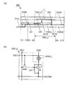
- FIG. 1 illustrates a structure of a display panel of one embodiment of the present invention.
- FIG. 1A is a top view of a display panel of one embodiment of the present invention
- FIG. 1B is a top view illustrating part of FIG.
- FIG. 2 illustrates a structure of a display panel of one embodiment of the present invention.
- 2A is a cross-sectional view taken along cutting lines X1-X2, X3-X4, and X9-X10 in FIG. 1A and pixels.
- FIG. 3 illustrates a structure of a display panel of one embodiment of the present invention.
- 3A is a cross-sectional view of the pixel in FIG. 1A
- FIG. 3B is a cross-sectional view illustrating part of FIG. 3A.
- FIG. 4 illustrates a structure of a display panel of one embodiment of the present invention.
- 4A is a cross-sectional view taken along cutting lines X1-X2 and X3-X4 in FIG. 1A
- FIG. 4B is a cross-sectional view illustrating part of FIG. 4A.
- FIG. 5 illustrates a structure of a display panel of one embodiment of the present invention.
- 5A is a cross-sectional view illustrating part of FIG. 3A
- FIG. 5B is a cross-sectional view illustrating part of FIG.
- a variable having an integer value of 1 or more may be used for the sign.
- (p) including a variable p that takes an integer value of 1 or more may be used as a part of a code that identifies any of the maximum p components.
- a variable m that takes an integer value of 1 or more and (m, n) including a variable n may be used as part of a code that identifies any of the maximum m ⁇ n components.
- a display panel 700 described in this embodiment includes a pixel 702 (i, j), a functional layer 520, and a heat dissipation member 510HS (see FIGS. 1A and 2A).
- the display panel 700 includes a flexible printed circuit board FPC1.
- the pixel 702 (i, j) includes a display element 650 (i, j) and a pixel circuit 530 (i, j).
- the pixel circuit 530 (i, j) is electrically connected to the display element 650 (i, j) (see FIGS. 2A and 2B).
- the pixel circuit 530 (i, j) is electrically connected to the scan line G2 (i) (see FIG. 2B).
- the functional layer 520 includes a pixel circuit 530 (i, j), a terminal 544, and an intermediate film 501B (see FIGS. 2A and 3A).
- the terminal 544 is connected to the display element 650 (i, j) (see FIG. 3A).
- the terminal 544 and the display element 650 (i, j) can be thermally connected using the bonding layer 544B in contact with the terminal 544 and the display element 650 (i, j).
- a material having a thermal conductivity of 0.5 W / m ⁇ K or more, preferably 1 W / m ⁇ K or more, more preferably 5 W / m ⁇ K or more can be used for the bonding layer 544B.
- the display element 650 (i, j) and the terminal 544 can be thermally connected to each other by using solder or a conductive paste for the bonding layer 544B.
- the bonding layer 541 (i, j) B that electrically connects the display element 650 (i, j) and the terminal 541 (i, j) the display element 650 (i, j) and the terminal are formed.
- a bonding layer 544B that thermally connects 544 can be formed.
- the intermediate film 501B includes an opening 591D.
- an opening 591A and an opening 591C are provided.
- a film with a thickness of 50 nm to 600 nm, preferably 50 nm to 200 nm can be used for the intermediate film 501B.
- a film containing silicon, oxygen, and nitrogen with a thickness of 200 nm can be used for the intermediate film 501B.
- Heat dissipation member 510HS is connected to terminal 544 at opening 591D.
- a material having a thermal conductivity of 1 W / m ⁇ K or more, preferably 10 W / m ⁇ K or more, more preferably 100 W / m ⁇ K or more can be used for the heat dissipation member 510HS.
- metal or ceramics can be used for the heat dissipation member 510HS.
- a metal such as copper or aluminum, or a ceramic such as aluminum nitride or silicon carbide can be used.
- the surface area on the side not in contact with the bonding layer 505 is made larger than the surface area on the side in contact with the bonding layer 505.
- heat can be discharged from the side not in contact with the bonding layer 505.
- heat may be exhausted to the atmosphere, and the heat radiating member 510HS may be cooled using a refrigerant.
- junction Layer 505 The bonding layer 505 is sandwiched between the terminal 544 and the heat dissipation member 510HS. Thereby, the terminal 544 and the heat radiating member 510HS can be thermally connected.
- an epoxy resin an acrylic resin, a silicone resin, a phenol resin, a polyimide resin, an imide resin, a PVC (polyvinyl chloride) resin, a PVB (polyvinyl butyral) resin, an EVA (ethylene vinyl acetate) resin, or the like is used as the bonding layer 505.
- an epoxy resin an acrylic resin, a silicone resin, a phenol resin, a polyimide resin, an imide resin, a PVC (polyvinyl chloride) resin, a PVB (polyvinyl butyral) resin, an EVA (ethylene vinyl acetate) resin, or the like is used as the bonding layer 505.
- PVC polyvinyl chloride
- PVB polyvinyl butyral
- EVA ethylene vinyl acetate
- a composition including a resin and particles having a spherical shape, a columnar shape, a filler shape, or the like can be used for the bonding layer 505.
- a composition including a resin and particles of a material having a higher thermal conductivity than the resin can be used for the bonding layer 505.
- a composition including metal particles or ceramic particles can be used for the bonding layer 505.
- a composition containing metal particles such as silver, copper, and aluminum and ceramic particles such as alumina, aluminum nitride, silicon carbide, and graphite can be used for the bonding layer 505.
- a composition containing particles at a volume filling rate of 40% or more, preferably 60% or more, more preferably 70% or more can be used for the bonding layer 505.
- the thermal conductivity of the bonding layer 505 can be increased.
- a material having a thermal conductivity of 0.5 W / m ⁇ K or more, preferably 1 W / m ⁇ K or more, more preferably 5 W / m ⁇ K or more can be used for the bonding layer 505.
- the heat radiating member 510HS and the display element 650 (i, j) can be connected.
- the heat generated by the display element 650 (i, j) can be transmitted to the heat dissipation member 510HS.
- the display element 650 (i, j) can be cooled using the heat dissipation member 510HS.
- the temperature increase of the display element 650 (i, j) can be suppressed.
- luminance accompanying a temperature rise can be suppressed.
- the reliability of the display element 650 (i, j) can be increased. As a result, a novel display panel that is highly convenient or reliable can be provided.
- the functional layer 520 includes a thermally conductive film 519B (1) (see FIGS. 5A and 5B).
- the thermally conductive film 519B (1) is thermally connected to the terminal 544, and the thermally conductive film 519B (1) overlaps with the opening 591D.
- the heat conductive film 519B (2) may be sandwiched between the heat conductive film 519B (1) and the terminal 544.
- the intermediate film 501B includes a surface 501B (1). Note that the surface 501B (1) faces the surface 501B (2), and the surface 501B (1) is located on the pixel circuit 530 (i, j) side from the surface 501B (2) (FIG. 3A and FIG. 3). 5 (A)).
- the surface 501B (1) includes a region 501B (11).
- the region 501B (11) is located at the periphery of the opening 591D, and the region 501B (11) is in contact with the thermally conductive film 519B (1). Note that the film 519B (1) is exposed in the opening 591D and thermally connects the heat dissipation member 510HS and the film 519B (1) through the bonding layer 505.
- the opening 591D includes a side end 501B (3), and the side end 501B (3) is in contact with the film 519B (1) (see FIG. 5B).
- heat generated by the display element 650 (i, j) can be transmitted to the thermally conductive film 519B (1).
- the heat generated by the display element 650 (i, j) can be transmitted to the heat radiating member 510HS.
- diffusion of impurities that impair reliability from the outside to the pixel 702 (i, j) can be suppressed by using the heat conductive film 519B (1) or the intermediate film.
- diffusion of impurities that impair reliability to the pixel circuit 530 (i, j) or diffusion to the display element 650 (i, j) can be suppressed.
- a novel display panel that is highly convenient or reliable can be provided.
- the film of the heat conductive film 519B (1) contains titanium, and the region 501B (11) contains silicon, oxygen, and fluorine.
- the thermally conductive film 519B (1) includes tungsten, and the region 501B (11) includes silicon, oxygen, and nitrogen.
- the intermediate film 501B includes a region 501B (12).
- the region 501B (12) is in close contact with another structure of the functional layer 520 with a force larger than the adhesion force of the region 501B (11) to the film 519B (1).
- the insulating film 501C is in close contact with the region 501B (12) of the intermediate film 501B (see FIG. 5A).
- the force with which the region 501B (12) is in close contact with the insulating film 501C is larger than the force with which the region 501B (11) is in close contact with the film 519B (1).
- the adhesion strength of the region 501B (12) and the adhesion strength of the region 501B (11) are compared. Specifically, the pressure of the indenter required for damaging the region 501B (11) is lower than the pressure of the indenter required for damaging the region 501B (12). For example, the indenter is moved from the region 501B (12) toward the region 501B (11) to compare the ease of damage.
- strength of the opening part 591D with respect to external force can be raised. Or it can be made hard to break. Diffusion of impurities that impair reliability from the outside to the pixel 702 (i, j) can be suppressed by using the heat conductive film 519B (1) or the intermediate film. Alternatively, diffusion of impurities that impair reliability to the pixel circuit 530 (i, j) or the display element 650 (i, j) can be suppressed. As a result, a novel display panel that is highly convenient or reliable can be provided.
- ⁇ Configuration of Pixel Circuit 530 (i, j) For example, a switch, a transistor, a diode, a resistor, an inductor, a capacitor, or the like can be used for the pixel circuit 530 (i, j).
- the pixel circuit 530 (i, j) includes a switch SW2, a transistor M, and a capacitor C21.
- a transistor can be used for the switch SW2.
- a bottom-gate transistor, a top-gate transistor, or the like can be used for the pixel circuit 530 (i, j).
- the transistor includes a semiconductor film 508, a conductive film 504, a conductive film 512A, and a conductive film 512B (see FIG. 3B).
- the semiconductor film 508 includes a region 508A electrically connected to the conductive film 512A and a region 508B electrically connected to the conductive film 512B.
- the semiconductor film 508 includes a region 508C between the region 508A and the region 508B.
- the conductive film 504 includes a region overlapping with the region 508C, and the conductive film 504 functions as a gate electrode.
- the insulating film 506 includes a region sandwiched between the semiconductor film 508 and the conductive film 504.
- the insulating film 506 has a function of a gate insulating film.
- the conductive film 512A has one of a source electrode function and a drain electrode function, and the conductive film 512B has another function of the source electrode and the drain electrode.
- the conductive film 524 can be used for a transistor.
- the conductive film 524 includes a region in which the semiconductor film 508 is sandwiched between the conductive film 504 and the conductive film 504.
- the conductive film 524 has a function of a second gate electrode.
- the conductive film 524 can be electrically connected to the conductive film 504. Note that the conductive film 524 can be used for the scan line G2 (i).
- Transistor M ⁇ Configuration Example 1 of Transistor M ⁇
- the same structure as the transistor used for the switch SW2 can be used for the transistor M.
- a semiconductor film that can be formed in the same process as the semiconductor film included in the transistor used for the switch SW2 can be used for the transistor M.
- the conductive films 512C and 512D can be used for the transistor M.
- Configuration Example 1 of Semiconductor Film 508 For example, a semiconductor containing a Group 14 element can be used for the semiconductor film 508. Specifically, a semiconductor containing silicon can be used for the semiconductor film 508.
- Hydroated amorphous silicon can be used for the semiconductor film 508.
- microcrystalline silicon or the like can be used for the semiconductor film 508. Accordingly, for example, a display panel with less display unevenness than a display panel using polysilicon as the semiconductor film 508 can be provided. Alternatively, the display panel can be easily increased in size.
- polysilicon can be used for the semiconductor film 508. Accordingly, for example, the field-effect mobility of the transistor can be higher than that of a transistor using hydrogenated amorphous silicon for the semiconductor film 508. Alternatively, for example, the driving ability can be increased as compared with a transistor using hydrogenated amorphous silicon for the semiconductor film 508. Alternatively, for example, the aperture ratio of the pixel can be improved over a transistor using hydrogenated amorphous silicon for the semiconductor film 508.
- the reliability of the transistor can be higher than that of a transistor using hydrogenated amorphous silicon for the semiconductor film 508.
- the temperature required for manufacturing the transistor can be lower than that of a transistor using single crystal silicon, for example.
- the semiconductor film used for the transistor of the driver circuit can be formed in the same process as the semiconductor film used for the transistor of the pixel circuit.
- the driver circuit can be formed over the same substrate as the pixel circuit. Alternatively, the number of parts included in the electronic device can be reduced.
- single crystal silicon can be used for the semiconductor film. Accordingly, for example, the definition can be increased as compared with a display panel using hydrogenated amorphous silicon for the semiconductor film 508. Alternatively, for example, a display panel with less display unevenness can be provided than a display panel using polysilicon as the semiconductor film 508. Or, for example, smart glasses or head mounted displays can be provided.
- a metal oxide can be used for the semiconductor film 508. Accordingly, as compared with a pixel circuit using a transistor using amorphous silicon as a semiconductor film, the time during which the pixel circuit can hold an image signal can be lengthened. Specifically, the selection signal can be supplied at a frequency of less than 30 Hz, preferably less than 1 Hz, more preferably less than once per minute while suppressing the occurrence of flicker. As a result, fatigue accumulated in the user of the information processing apparatus can be reduced. In addition, power consumption associated with driving can be reduced.
- a transistor including an oxide semiconductor can be used.
- an oxide semiconductor containing indium or an oxide semiconductor containing indium, gallium, and zinc can be used for the semiconductor film.
- a transistor whose leakage current in an off state is smaller than that of a transistor using amorphous silicon as a semiconductor film can be used.
- a transistor in which an oxide semiconductor is used for a semiconductor film can be used.
- a 25-nm-thick film containing indium, gallium, and zinc can be used for the semiconductor film 508.
- a conductive film in which a 10-nm-thick film containing tantalum and nitrogen and a 300-nm-thick film containing copper are stacked can be used for the conductive film 504.
- the film containing copper includes a region between which the film containing tantalum and nitrogen is sandwiched between the film containing copper.
- a stacked film in which a 400-nm-thick film containing silicon and nitrogen and a 200-nm-thick film containing silicon, oxygen, and nitrogen are stacked can be used for the insulating film 506.
- the film containing silicon and nitrogen includes a region between the semiconductor film 508 and the film containing silicon, oxygen, and nitrogen.
- the film containing tungsten includes a region in contact with the semiconductor film 508.
- a bottom-gate transistor production line using amorphous silicon as a semiconductor can be easily modified to a bottom-gate transistor production line using an oxide semiconductor as a semiconductor.
- a top-gate transistor production line using polysilicon as a semiconductor can be easily modified to a top-gate transistor production line using an oxide semiconductor as a semiconductor. Both modifications can make effective use of existing production lines.
- a compound semiconductor can be used for a semiconductor of a transistor.
- a semiconductor containing gallium arsenide can be used.
- an organic semiconductor can be used for a semiconductor of a transistor.
- an organic semiconductor containing polyacenes or graphene can be used for the semiconductor film.
- the functional layer 520 includes an insulating film 521, an insulating film 518, an insulating film 516, an insulating film 506, an insulating film 501C, and the like (see FIG. 3A).
- the insulating film 521 includes a region sandwiched between the display element 650 (i, j) and the insulating film 501C.
- the insulating film 518 includes a region sandwiched between the insulating film 521 and the insulating film 501C.
- the insulating film 516 includes a region sandwiched between the insulating film 518 and the insulating film 501C.
- the insulating film 506 includes a region sandwiched between the insulating film 516 and the insulating film 501C.
- Insulating film 521 For example, an insulating inorganic material, an insulating organic material, or an insulating composite material containing an inorganic material and an organic material can be used for the insulating film 521.
- the insulating film 521 can be formed using an inorganic oxide film, an inorganic nitride film, an inorganic oxynitride film, or the like, or a stacked material in which a plurality selected from these is stacked.
- the insulating film 521 can be a silicon oxide film, a silicon nitride film, a silicon oxynitride film, an aluminum oxide film, or the like, or a film including a stacked material in which a plurality of layers selected from these is stacked.
- the silicon nitride film is a dense film and has an excellent function of suppressing impurity diffusion.
- the insulating film 521 can planarize steps resulting from various structures overlapping with the insulating film 521, for example.
- polyimide has characteristics superior to other organic materials in characteristics such as thermal stability, insulation, toughness, low dielectric constant, low thermal expansion coefficient, and chemical resistance. Thereby, polyimide can be suitably used for the insulating film 521 and the like.
- a film formed using a photosensitive material can be used for the insulating film 521.
- a film formed using photosensitive polyimide, photosensitive acrylic resin, or the like can be used for the insulating film 521.
- Insulating film 518 For example, a material that can be used for the insulating film 521 can be used for the insulating film 518.
- a material having a function of suppressing diffusion of oxygen, hydrogen, water, alkali metal, alkaline earth metal, or the like can be used for the insulating film 518.
- a nitride insulating film can be used for the insulating film 518.
- silicon nitride, silicon nitride oxide, aluminum nitride, aluminum nitride oxide, or the like can be used for the insulating film 518. Thereby, diffusion of impurities into the semiconductor film of the transistor can be suppressed.
- Insulating film 516 For example, a material that can be used for the insulating film 521 can be used for the insulating film 516.
- the insulating film 516A and the insulating film 516B can be used for the insulating film 516.
- a film whose manufacturing method is different from that of the insulating film 518 can be used for the insulating film 516.
- Insulating film 506 For example, a material that can be used for the insulating film 521 can be used for the insulating film 506 or the insulating film 501D.
- a film including a lanthanum oxide film, a cerium oxide film, or a neodymium oxide film can be used for the insulating film 506.
- the insulating film 501D includes a region sandwiched between the insulating film 501C and the insulating film 516 (see FIG. 3B).
- a material that can be used for the insulating film 506 can be used for the insulating film 501D.
- a material that can be used for the insulating film 521 can be used for the insulating film 501C.
- a material containing silicon and oxygen can be used for the insulating film 501C.
- the display panel 700 includes a base material 770 and a sealing material 705 (see FIG. 3A).
- Substrate 770 A material having a light-transmitting property can be used for the base material 770.
- a flexible material can be used for the base material 770.
- a flexible display panel can be provided.
- a material having a thickness of 0.7 mm or less and a thickness of 0.1 mm or more can be used.
- a material polished to a thickness of about 0.1 mm can be used. Thereby, a weight can be reduced.
- glass substrates of 6th generation (1500 mm ⁇ 1850 mm), 7th generation (1870 mm ⁇ 2200 mm), 8th generation (2200 mm ⁇ 2400 mm), 9th generation (2400 mm ⁇ 2800 mm), 10th generation (2950 mm ⁇ 3400 mm), etc. can be used for the substrate 770.
- a large display device can be manufactured.
- An organic material, an inorganic material, or a composite material such as an organic material and an inorganic material can be used for the base material 770.
- inorganic materials such as glass, ceramics, and metal can be used.
- alkali-free glass, soda-lime glass, potash glass, crystal glass, aluminosilicate glass, tempered glass, chemically tempered glass, quartz, sapphire, or the like can be used for the base material 770.
- aluminosilicate glass, tempered glass, chemically tempered glass, sapphire, or the like can be suitably used for the base material 770 disposed on the side closer to the user of the display panel. Thereby, it is possible to prevent the display panel from being damaged or damaged due to use.
- an inorganic oxide film, an inorganic nitride film, an inorganic oxynitride film, or the like can be used.
- a silicon oxide film, a silicon nitride film, a silicon oxynitride film, an aluminum oxide film, or the like can be used.
- Stainless steel, aluminum, or the like can be used for the base material 770.
- a single crystal semiconductor substrate made of silicon or silicon carbide, a polycrystalline semiconductor substrate, a compound semiconductor substrate such as silicon germanium, an SOI substrate, or the like can be used for the base material 770.
- a semiconductor element can be formed on the base material 770.
- an organic material such as a resin, a resin film, or plastic can be used for the base 770.
- a material including polyester, polyolefin, polyamide (nylon, aramid, or the like), polyimide, polycarbonate, polyurethane, an acrylic resin, an epoxy resin-containing resin, or a resin having a siloxane bond can be used for the base material 770.
- a resin film, a resin plate, or a laminated material containing these materials can be used. Thereby, a weight can be reduced. Or, for example, it is possible to reduce the frequency of occurrence of breakage due to dropping.
- PET polyethylene terephthalate
- PEN polyethylene naphthalate
- PES polyethersulfone
- COP cycloolefin polymer
- COC cycloolefin copolymer
- a composite material in which a film such as a metal plate, a thin glass plate, or an inorganic material and a resin film are bonded to each other can be used for the base material 770.
- a composite material in which a fibrous or particulate metal, glass, inorganic material, or the like is dispersed in a resin can be used for the base material 770.
- a composite material in which a fibrous or particulate resin, an organic material, or the like is dispersed in an inorganic material can be used for the base material 770.
- a single layer material or a material in which a plurality of layers are stacked can be used for the base material 770.
- a material in which an insulating film or the like is stacked can be used.
- a material in which one or a plurality of films selected from a silicon oxide layer, a silicon nitride layer, a silicon oxynitride layer, or the like is stacked can be used.
- diffusion of impurities contained in the base material can be prevented.
- diffusion of impurities contained in glass or resin can be prevented.
- diffusion of impurities that permeate the resin can be prevented.
- paper, wood, or the like can be used for the base material 770.
- a material having heat resistance high enough to withstand heat treatment in the manufacturing process can be used for the base material 770.
- a material having heat resistance to heat applied during a manufacturing process for directly forming a transistor, a capacitor, or the like can be used for the base material 770.
- an insulating film, a transistor, a capacitor, or the like is formed over a process substrate that is resistant to heat applied during the manufacturing process, and the formed insulating film, transistor, capacitor, or the like is transferred to the base material 770, for example.
- the method can be used. Accordingly, for example, an insulating film, a transistor, a capacitor, or the like can be formed over a flexible substrate.
- the sealing material 705 includes a region sandwiched between the functional layer 520 and the base material 770 and has a function of bonding the functional layer 520 and the base material 770 together.
- An inorganic material, an organic material, a composite material of an inorganic material and an organic material, or the like can be used for the sealant 705.
- an organic material such as a heat-meltable resin or a curable resin can be used for the sealing material 705.
- an organic material such as a reactive curable adhesive, a photocurable adhesive, a thermosetting adhesive, and / or an anaerobic adhesive can be used for the sealant 705.
- an adhesive including epoxy resin, acrylic resin, silicone resin, phenol resin, polyimide resin, imide resin, PVC (polyvinyl chloride) resin, PVB (polyvinyl butyral) resin, EVA (ethylene vinyl acetate) resin, etc. Can be used for the sealant 705.
- the display panel 700 includes a functional film 770P (see FIG. 3A). In addition, a light shielding film BM is provided.
- the functional film 770P includes a region overlapping with the display element 650 (i, j).
- an antireflection film for example, an antireflection film, a polarizing film, a retardation film, a light diffusion film, a light collecting film, or the like can be used for the functional film 770P.
- an antireflection film having a thickness of 1 ⁇ m or less can be used for the functional film 770P.
- a multilayer film in which three or more dielectric layers, preferably five or more layers, more preferably 15 or more layers are stacked can be used for the functional film 770P. Thereby, a reflectance can be suppressed to 0.5% or less, preferably 0.08% or less.
- a circularly polarizing film can be used for the functional film 770P.
- antistatic film that suppresses adhesion of dust
- water-repellent film that makes it difficult to adhere dirt
- antireflection film anti-reflection film
- non-glossy film anti-glare film
- scratches caused by use A hard coat film or the like that suppresses the above can be used for the functional film 770P.
- the display element 650 (i, j) has a function of emitting light.
- a light-emitting diode, an organic electroluminescence element, an inorganic electroluminescence element, a QDLED (Quantum Dot LED), or the like can be used for the display element 650 (i, j).
- a light-emitting diode having a horizontal structure or a light-emitting diode having a vertical structure can be used for the display element 650 (i, j).
- a micro LED can be used for the display element 650 (i, j).
- area of the region for emitting light 1 mm 2 or less, preferably 10000 2 or less, more preferably 3000 .mu.m 2 or less, more preferably used in view the micro LED device 650 (i, j) is 700 .mu.m 2 or less be able to.
- the display element 650 includes, for example, a P-type cladding layer, an N-type cladding layer, and a light-emitting layer, and the light-emitting layer includes a region sandwiched between the P-type cladding layer and the N-type cladding layer.
- a stack material laminated to emit blue light, a laminate material laminated to emit green light, a laminate material laminated to emit red light, or the like is used as the display element 650 ( i, j).
- a gallium / phosphorus compound, a gallium / arsenic compound, a gallium / aluminum / arsenic compound, an aluminum / gallium / indium / phosphorus compound, an indium / gallium nitride compound, or the like is used for the display element 650 (i, j). Can do.
- the color conversion layer can be used for the display element 650 (i, j).
- the color conversion layer has a function of absorbing the color of light emitted from the light emitting layer and emitting light of different colors.
- the color conversion layer has a function of absorbing blue light emitted from the light emitting layer and emitting yellow light. Thereby, the yellow light emitted from the color conversion layer and the blue light transmitted through the color conversion layer can be mixed. As a result, white light can be obtained.
- the color conversion layer has a function of absorbing near-ultraviolet light emitted from the light-emitting layer and emitting red light, green light, and blue light.
- a light emitting layer that emits near-ultraviolet light can be used for the display element 650 (i, j).
- the near ultraviolet light can be turned into white light.
- near-ultraviolet light can be made light with excellent color rendering properties.
- a phosphor can be used for the color conversion layer.
- quantum dots can be used for the color conversion layer. When a quantum dot is used for the color conversion layer, light of a bright color with a narrow half width can be emitted.
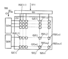
- FIG. 6 illustrates a structure of a display panel of one embodiment of the present invention.
- a display panel 700 described in this embodiment includes a display region 231 (see FIG. 6).
- the display region 231 includes a group of pixels 702 (i, 1) to 702 (i, n), another group of pixels 702 (1, j) to 702 (m, j), and a scanning line G2 (i ) And a signal line S2 (j) (see FIG. 6).
- i is an integer of 1 to m
- j is an integer of 1 to n
- m and n are integers of 1 or more.
- the display region 231 includes a conductive film VCOM2 and a conductive film ANO.
- the group of pixels 702 (i, 1) to 702 (i, n) are arranged in the row direction (the direction indicated by the arrow R1 in the figure), and the group of pixels 702 (i, 1) to 702 (i, n n) includes pixel 702 (i, j).
- Another group of pixels 702 (1, j) to 702 (m, j) is arranged in a column direction (direction indicated by an arrow C1 in the drawing) intersecting the row direction, and another group of pixels 702 (1 , J) through pixel 702 (m, j) include pixel 702 (i, j).
- the scan line G2 (i) is electrically connected to a group of the pixels 702 (i, 1) to 702 (i, n) arranged in the row direction.
- the signal line S2 (j) is electrically connected to another group of the pixels 702 (1, j) to 702 (m, j) arranged in the column direction.
- image information can be supplied to a plurality of pixels.
- a novel display panel that is highly convenient or reliable can be provided.
- the display area 231 includes 600 or more pixels per inch.
- the display area 231 includes a plurality of pixels in a matrix.
- the display area 231 includes 7600 or more pixels in the row direction, and the display area 231 includes 4300 or more pixels in the column direction. Specifically, 7680 pixels are provided in the row direction, and 4320 pixels are provided in the column direction.
- the display area 231 includes a plurality of pixels.
- the plurality of pixels have a function of displaying colors having different hues.
- hue colors that cannot be displayed by the pixels can be displayed by additive color mixing.
- each pixel can be referred to as a sub-pixel.
- a plurality of sub-pixels can be referred to as a pixel.
- the pixel 702 (i, j) can be rephrased as a sub-pixel, and the pixel 702 (i, j), the pixel 702 (i, j + 1), and the pixel 702 (i, j + 2) are combined into a pixel 703 ( i, k) (see FIG. 1C).
- a set of a subpixel that displays blue, a subpixel that displays green, and a subpixel that displays red can be used for the pixel 703 (i, k).
- a sub-pixel for displaying cyan, a sub-pixel for displaying magenta, and a sub-pixel for displaying yellow can be used as a set for the pixel 703 (i, k).
- a sub-pixel displaying white or the like can be used for the pixel in addition to the above set.
- the display region 231 includes a pixel 702 (i, j), a pixel 702 (i, j + 1), and a pixel 702 (i, j + 2) (see FIG. 1C).
- the pixel 702 (i, j) displays a color having a chromaticity x in the CIE 1931 chromaticity coordinates of greater than 0.680 and less than or equal to 0.720, and a chromaticity y of 0.260 to 0.320.
- the pixel 702 (i, j + 1) displays a color having a chromaticity x in the CIE 1931 chromaticity coordinates of 0.130 or more and 0.250 or less, and a chromaticity y of greater than 0.710 and 0.810 or less.
- the pixel 702 (i, j + 2) displays a color having a chromaticity x of 0.120 to 0.170 and a chromaticity y of 0.020 to less than 0.060 in the CIE 1931 chromaticity coordinates.
- the pixel 702 (i, j), the pixel 702 (i, j + 1), and the pixel 702 (i, j + 2) are represented by BT.
- the area ratio to the 2020 color gamut is 80% or more, or the coverage ratio to the color gamut is 75% or more.
- the area ratio is 90% or more, or the coverage is 85% or more.
- a display panel 700 described in this embodiment includes one or a plurality of driving circuits.
- a drive circuit GD and a drive circuit SD can be provided (see FIG. 6).
- Drive circuit GDA, drive circuit GDB can be used for the drive circuit GD.
- the drive circuit GDA and the drive circuit GDB have a function of supplying a selection signal based on the control information.
- a function of supplying a selection signal to one scanning line at a frequency of 30 Hz or more, preferably 60 Hz or more based on the control information is provided. Thereby, a moving image can be displayed smoothly.
- a function of supplying a selection signal to one scan line at a frequency of less than 30 Hz, preferably less than 1 Hz, more preferably less than once per minute based on the control information is provided. Thereby, a still image in which flicker is suppressed can be displayed.
- the frequency with which the drive circuit GDA supplies the selection signal and the frequency with which the drive circuit GDB supplies the selection signal can be made different.
- the selection signal can be supplied to another region displaying the moving image at a frequency higher than the frequency of supplying the selection signal to one region displaying the still image.
- the frame frequency can be made variable.
- display can be performed at a frame frequency of 1 Hz to 120 Hz.
- display can be performed at a frame frequency of 120 Hz using a progressive method.
- a bottom-gate transistor, a top-gate transistor, or the like can be used for the driver circuit GD.
- the transistor MD can be used for the drive circuit GD (see FIG. 4).
- a semiconductor film used for a transistor of the driver circuit GD can be formed in a step of forming a semiconductor film used for a transistor of the pixel circuit 530 (i, j).
- the drive circuit SD has a function of generating an image signal based on the information V11 and a function of supplying the image signal to a pixel circuit that is electrically connected to one display element (see FIG. 6).
- various sequential circuits such as a shift register can be used for the drive circuit SD.
- an integrated circuit formed on a silicon substrate can be used for the drive circuit SD.
- the integrated circuit can be connected to a terminal by using a COG (Chip on glass) method or a COF (Chip on Film) method.
- a COG Chip on glass
- COF Chip on Film
- an integrated circuit can be connected to a terminal using an anisotropic conductive film.
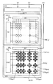
- FIG. 7 illustrates a structure of a display device of one embodiment of the present invention.
- FIG. 7A is a block diagram of a display device of one embodiment of the present invention
- FIGS. 7B-1 to 7B-3 are projections illustrating the appearance of the display device of one embodiment of the present invention.
- FIG. 7A is a block diagram of a display device of one embodiment of the present invention
- FIGS. 7B-1 to 7B-3 are projections illustrating the appearance of the display device of one embodiment of the present invention.
- FIG. 7A is a block diagram of a display device of one embodiment of the present invention
- FIGS. 7B-1 to 7B-3 are projections illustrating the appearance of the display device of one embodiment of the present invention.
- the display device described in this embodiment includes a control portion 238 and a display panel 700 (see FIG. 7A).
- the control unit 238 is supplied with the image information V1 and the control information CI.
- a clock signal or a timing signal can be used for the control information CI.
- the control unit 238 generates information V11 based on the image information V1, and generates a control signal SP based on the control information CI. In addition, the control unit 238 supplies information V11 and a control signal SP.
- the information V11 includes a gradation of 8 bits or more, preferably 12 bits or more.
- a clock signal or a start pulse of a shift register used for the driver circuit can be used for the control signal SP.
- control unit 238 includes a control circuit 233, an expansion circuit 234, and an image processing circuit 235.
- the expansion circuit 234 has a function of expanding the image information V1 supplied in a compressed state.
- the decompression circuit 234 includes a storage unit.
- the storage unit has a function of storing, for example, decompressed image information.
- the image processing circuit 235 includes a storage area, for example.
- the storage area has a function of storing information included in the image information V1, for example.
- the image processing circuit 235 includes, for example, a function of correcting the image information V1 based on a predetermined characteristic curve to generate information V11 and a function of supplying information V11.
- the display panel 700 is supplied with information V11 and a control signal SP.
- the display panel 700 includes a drive circuit GD.
- the display panel 700 described in Embodiment 1 or 2 can be used.
- control circuit 233 can be used for the display panel 700.
- a driver circuit can be used for the display panel 700.
- Control circuit 233 has a function of generating and supplying the control signal SP.
- a clock signal or a timing signal can be used as the control signal SP.
- a timing controller can be used for the control circuit 233.
- control circuit 233 formed over a rigid substrate can be used for the display panel 700.
- control circuit 233 and the control unit 238 formed on the rigid board can be electrically connected using a flexible printed board.
- the drive circuit GD operates based on the control signal SP.
- the drive circuit GDA (1), the drive circuit GDA (2), the drive circuit GDB (1), and the drive circuit GDB (2) are supplied with the control signal SP and have a function of supplying a selection signal.
- SDA (1), SDA (2), SDB (1), SDB (2), SDC (1), and SDC (2) are supplied with control signal SP and information V11, and supply an image signal. it can.
- control signal SP By using the control signal SP, the operations of the plurality of drive circuits can be synchronized.
- a novel display device that is highly convenient or reliable can be provided.
- a television receiving system see FIG. 7B-1
- a video monitor see FIG. 7B-2
- a notebook computer see FIG. 7B-3
- FIG. 8 is a block diagram illustrating a structure of the input / output device of one embodiment of the present invention.
- the input / output device described in this embodiment includes an input unit 240 and a display unit 230 (see FIG. 8).
- the display unit 230 includes a display panel.
- the display panel 700 described in Embodiment 1 or 2 can be used for the display portion 230.
- a structure including the input portion 240 and the display portion 230 can be referred to as an input / output panel 700TP.
- the input unit 240 includes a detection area 241.
- the input unit 240 has a function of detecting an object close to the detection area 241.
- the detection region 241 includes a region overlapping with the pixel 702 (i, j).
- position information can be input using a finger or the like that is brought close to the display portion as a pointer.
- the position information can be associated with image information displayed on the display unit.
- the input unit 240 includes an oscillation circuit OSC and a detection circuit DC (see FIG. 8). In addition, a conductive film CL (g) and a conductive film ML (h) are provided.
- the detection area 241 includes, for example, one or a plurality of detection elements.
- the detection region 241 includes a group of detection elements 775 (g, 1) to detection elements 775 (g, q) and another group of detection elements 775 (1, h) to detection elements 775 (p, h).
- g is an integer of 1 to p
- h is an integer of 1 to q
- p and q are integers of 1 or more.
- the group of sensing elements 775 (g, 1) to 775 (g, q) includes the sensing elements 775 (g, h) and are arranged in the row direction (direction indicated by an arrow R2 in the drawing).
- the direction indicated by arrow R2 may be the same as or different from the direction indicated by arrow R1.
- another group of the detection elements 775 (1, h) to 775 (p, h) includes the detection elements 775 (g, h), and the column direction (in the drawing, indicated by an arrow C2) that intersects the row direction. (Direction shown).
- the detection element has a function of detecting an adjacent pointer.
- a finger or a stylus pen can be used as the pointer.
- a metal piece or a coil can be used for the stylus pen.
- a capacitive proximity sensor an electromagnetic induction proximity sensor, an optical proximity sensor, a resistive proximity sensor, or the like can be used as the detection element.
- a plurality of types of sensing elements can also be used in combination.
- a detection element that detects a finger and a detection element that detects a stylus pen can be used in combination.
- the type of the pointer can be determined.
- different instructions can be associated with the detection information based on the determined type of pointer. Specifically, when it is determined that a finger is used as the pointer, the detection information can be associated with the gesture. Alternatively, when it is determined that the stylus pen is used as the pointer, the detection information can be associated with the drawing process.
- a finger can be detected by using a capacitive or optical proximity sensor.
- the stylus pen can be detected using an electromagnetic induction type or optical type proximity sensor.
- FIG. 9A is a block diagram illustrating a structure of an information processing device of one embodiment of the present invention.
- FIG. 9B and FIG. 9C are projection views for explaining an example of the appearance of the information processing apparatus.
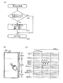
- FIG. 10 is a flowchart illustrating a program according to one embodiment of the present invention.
- FIG. 10A is a flowchart illustrating main processing of a program according to one embodiment of the present invention
- FIG. 10B is a flowchart illustrating interrupt processing.
- FIG. 11 is a diagram illustrating a program according to one embodiment of the present invention.
- FIG. 11A is a flowchart illustrating a program interrupt process according to one embodiment of the present invention.
- FIG. 11B is a schematic diagram illustrating the operation of the information processing device, and
- FIG. 11C is a timing chart illustrating the operation of the information processing device of one embodiment of the present invention.
- the information processing device described in this embodiment includes an arithmetic device 210 and an input / output device 220 (see FIG. 9A). Note that the input / output device is electrically connected to the arithmetic device 210. Further, the information processing device 200 can include a housing (see FIG. 9B or FIG. 9C).
- the arithmetic unit 210 is supplied with the input information II or the detection information DS.
- the arithmetic unit 210 generates control information CI and image information V1 based on the input information II or detection information DS, and supplies the control information CI and image information V1.
- the calculation device 210 includes a calculation unit 211 and a storage unit 212.
- the arithmetic unit 210 includes a transmission path 214 and an input / output interface 215.
- the transmission path 214 is electrically connected to the calculation unit 211, the storage unit 212, and the input / output interface 215.
- the calculation unit 211 has a function of executing a program, for example.
- Storage unit 212 has a function of storing, for example, a program executed by the calculation unit 211, initial information, setting information, or an image.
- a hard disk a flash memory, a memory including a transistor including an oxide semiconductor, or the like can be used.
- the input / output interface 215 includes a terminal or a wiring, and has a function of supplying information and receiving information.
- the transmission line 214 can be electrically connected.
- the input / output device 220 can be electrically connected.
- the transmission path 214 includes wiring, supplies information, and has a function of being supplied with information.
- the input / output interface 215 can be electrically connected. Further, it can be electrically connected to the calculation unit 211, the storage unit 212, or the input / output interface 215.
- the input / output device 220 supplies input information II and detection information DS.
- the input / output device 220 is supplied with the control information CI and the image information V1 (see FIG. 9A).
- a keyboard scan code, position information, button operation information, audio information, or image information can be used as the input information II.
- illuminance information such as an environment in which the information processing apparatus 200 is used, posture information, acceleration information, azimuth information, pressure information, temperature information, or humidity information can be used as the detection information DS.
- a signal for controlling the luminance for displaying the image information V1 a signal for controlling the saturation, and a signal for controlling the hue can be used as the control information CI.
- a signal that changes the display of a part of the image information V1 can be used for the control information CI.
- the input / output device 220 includes a display unit 230, an input unit 240, and a detection unit 250.
- the input / output device described in Embodiment 4 can be used.
- the display unit 230 displays the image information V1 based on the control information CI.
- the display unit 230 includes a control unit 238, a drive circuit GD, a drive circuit SD, and a display panel 700 (see FIG. 7).
- a control unit 238, a drive circuit GD, a drive circuit SD, and a display panel 700 see FIG. 7.
- the display device described in Embodiment 3 can be used for the display portion 230.
- the input unit 240 generates input information II.
- the input unit 240 has a function of supplying the position information P1.
- a human interface or the like can be used for the input unit 240 (see FIG. 9A).
- a keyboard, a mouse, a touch sensor, a microphone, a camera, or the like can be used for the input unit 240.
- a touch sensor including a region overlapping with the display portion 230 can be used.
- an input / output device including a touch sensor including a display unit 230 and a region overlapping with the display unit 230 can be referred to as a touch panel or a touch screen.
- the user can make various gestures (tap, drag, swipe, pinch in, etc.) using a finger touching the touch panel as a pointer.
- various gestures tap, drag, swipe, pinch in, etc.
- the computing device 210 may analyze information such as the position or locus of a finger that touches the touch panel, and a predetermined gesture may be supplied when the analysis result satisfies a predetermined condition. Accordingly, the user can supply a predetermined operation command associated with the predetermined gesture in advance using the gesture.
- the user can supply a “scroll command” for changing the display position of the image information using a gesture for moving a finger that touches the touch panel along the touch panel.
- the detection unit 250 generates detection information DS.
- the detection unit 250 has a function of detecting illuminance of an environment where the information processing apparatus 200 is used, and a function of supplying illuminance information.
- the detection unit 250 has a function of detecting surrounding conditions and supplying detection information. Specifically, illuminance information, posture information, acceleration information, azimuth information, pressure information, temperature information, humidity information, or the like can be supplied.
- a light detector for example, a light detector, an attitude detector, an acceleration sensor, an orientation sensor, a GPS (Global positioning System) signal receiving circuit, a pressure sensor, a temperature sensor, a humidity sensor, a camera, or the like can be used for the detection unit 250.
- a GPS Global positioning System
- the communication unit 290 has a function of supplying information to the network and acquiring information from the network.
- the housing has a function of housing the input / output device 220 or the arithmetic device 210.
- the housing has a function of supporting the display unit 230 or the arithmetic device 210.
- control information can be generated based on input information or detection information.
- image information can be displayed based on input information or detection information.
- the information processing apparatus can operate by grasping the intensity of light received by the housing of the information processing apparatus in an environment where the information processing apparatus is used.
- the user of the information processing apparatus can select a display method.
- a touch panel in which a touch sensor is superimposed on a display panel is not only a display unit but also an input unit.
- the arithmetic device 210 includes an artificial intelligence unit 213 (see FIG. 9A).
- the artificial intelligence unit 213 generates control information CI based on the input information II or the detection information DS.
- the artificial intelligence unit 213 can perform natural language processing on the input information II and extract one feature from the entire input information II. For example, the artificial intelligence unit 213 can infer and characterize emotions and the like included in the input information II. In addition, it is possible to infer a color, pattern, or typeface that is empirically felt to be suitable for the feature. In addition, the artificial intelligence unit 213 can generate information for designating a character color, a pattern or a typeface, and information for designating a background color or a pattern, and use them for the control information CI.
- the artificial intelligence unit 213 can perform natural language processing on the input information II and extract some words included in the input information II. For example, the artificial intelligence unit 213 can extract grammatical errors, factual misconceptions, or expressions including emotions. In addition, the artificial intelligence unit 213 can generate information for displaying the extracted part in a color, pattern, or typeface that is different from the other part, and can use it for the control information CI.
- the artificial intelligence unit 213 can perform image processing on the input information II and extract one feature from the input information II. For example, the artificial intelligence unit 213 can infer and characterize the age when the input information II was photographed, indoor or outdoor, day or night, and the like. Further, it is possible to infer a color tone that is empirically felt to be suitable for the feature, and to generate control information CI for using the color tone for display. Specifically, information that specifies a color (for example, full color, black and white, brown, or the like) that is used for expression of shading can be used as the control information CI.
- a color for example, full color, black and white, brown, or the like
- the artificial intelligence unit 213 can perform image processing on the input information II and extract a part of the image included in the input information II. For example, it is possible to generate control information CI that displays a boundary between a part of the extracted image and another part. Specifically, it is possible to generate control information CI that displays a rectangle surrounding a part of the extracted image.
- the artificial intelligence unit 213 can generate an inference using the detection information DS.
- the control information CI can be generated based on the inference RI so that the user of the information processing apparatus 200 feels comfortable.
- the artificial intelligence unit 213 can generate the control information CI for adjusting the display brightness so that the brightness of the display is felt comfortable based on the illuminance of the environment and the like.
- the artificial intelligence unit 213 can generate the control information CI for adjusting the volume so that the size is felt comfortable based on environmental noise and the like.
- a clock signal or timing signal supplied to the control unit 238 included in the display unit 230 can be used for the control information CI.
- a clock signal or a timing signal supplied to the control unit included in the input unit 240 can be used for the control information CI.
- program The program of one embodiment of the present invention includes the following steps (see FIG. 10A).
- predetermined image information to be displayed at startup a predetermined mode for displaying the image information, and information for specifying a predetermined display method for displaying the image information are acquired from the storage unit 212.
- one still image information or other moving image information can be used as predetermined image information.
- the first mode or the second mode can be used as a predetermined mode.
- interrupt processing is permitted (see FIGS. 10A and S2).
- an arithmetic unit that is permitted to perform interrupt processing can perform interrupt processing in parallel with main processing.
- the arithmetic unit that has returned to the main process from the interrupt process can reflect the result obtained by the interrupt process to the main process.
- the arithmetic unit performs interrupt processing, and when returning from the interrupt processing, the counter may be set to a value other than the initial value. As a result, interrupt processing can always be performed after the program is started.
- the image information is displayed using a predetermined mode or a predetermined display method selected in the first step or the interruption process (see FIGS. 10A and S3).
- the predetermined mode specifies a mode for displaying information
- the predetermined display method specifies a method for displaying image information. Further, for example, it can be used as information for displaying the image information V1.
- one method for displaying the image information V1 can be associated with the first mode.
- another method for displaying the image information V1 can be associated with the second mode. Thereby, a display method can be selected based on the selected mode.
- a method of supplying a selection signal to one scanning line at a frequency of 30 Hz or more, preferably 60 Hz or more, and displaying based on the selection signal can be associated with the first mode.
- the selection signal when the selection signal is supplied at a frequency of 30 Hz or higher, preferably 60 Hz or higher, the motion of the moving image can be displayed smoothly.
- an image when an image is updated at a frequency of 30 Hz or higher, preferably 60 Hz or higher, an image that changes so as to smoothly follow the user's operation can be displayed on the information processing apparatus 200 being operated by the user.
- Second mode a method for supplying a selection signal to one scanning line at a frequency of less than 30 Hz, preferably less than 1 Hz, more preferably less than once per minute, and performing display based on the selection signal, Can be associated with a mode.
- the selection signal is supplied at a frequency of less than 30 Hz, preferably less than 1 Hz, more preferably less than once per minute, a display in which flicker or flicker is suppressed can be displayed. In addition, power consumption can be reduced.
- the display can be updated at a frequency of once per second or a frequency of once per minute.
- the light-emitting element when a light-emitting element is used as a display element, the light-emitting element can emit light in a pulse shape to display image information.
- the organic EL element can emit light in a pulse shape, and the afterglow can be used for display. Since the organic EL element has excellent frequency characteristics, there are cases where the time for driving the light emitting element can be shortened and the power consumption can be reduced. Alternatively, heat generation is suppressed, so that deterioration of the light-emitting element can be reduced in some cases.
- an end command supplied in the interrupt process may be used for determination.
- the interrupt process includes the following sixth to eighth steps (see FIG. 10B).
- the detection unit 250 is used to detect the illuminance of the environment in which the information processing apparatus 200 is used (see FIGS. 10B and S6). Note that the color temperature or chromaticity of the ambient light may be detected instead of the illuminance of the environment.
- a display method is determined based on the detected illuminance information (see FIGS. 10B and S7). For example, the display brightness is determined not to be too dark or too bright.
- the display color may be adjusted.
- FIG. 11A is a flowchart illustrating a program of one embodiment of the present invention.
- FIG. 11A is a flowchart for explaining an interrupt process different from the interrupt process shown in FIG.
- the configuration example 3 of the information processing device is different from the interrupt processing described with reference to FIG. 10B in that the interrupt processing includes a step of changing the mode based on the supplied predetermined event.
- the interrupt processing includes a step of changing the mode based on the supplied predetermined event.
- the interrupt process includes the following sixth to eighth steps (see FIG. 11A).
- the process proceeds to the seventh step, and if the predetermined event is not supplied, the process proceeds to the eighth step (see FIGS. 11A and U6). ).
- the predetermined period can be a period of 5 seconds or less, 1 second or less, or 0.5 seconds or less, preferably 0.1 seconds or less and longer than 0 seconds.
- the mode is changed (see FIGS. 11A and U7). Specifically, when the first mode is selected, the second mode is selected, and when the second mode is selected, the first mode is selected.
- the display mode can be changed for some areas of the display unit 230. Specifically, the display mode can be changed for a region where one driver circuit of the display portion 230 including the driver circuit GDA, the driver circuit GDB, and the driver circuit GDC supplies a selection signal (see FIG. 11B). ).
- the display mode of the area where the drive circuit GDB supplies the selection signal may be changed.
- the frequency of the selection signal supplied by the drive circuit GDB can be changed according to a “tap” event supplied to the touch panel using a finger or the like.
- Signal GCLK is a clock signal for controlling the operation of drive circuit GDB
- signal PWC1 and signal PWC2 are pulse width control signals for controlling the operation of drive circuit GDB.
- the drive circuit GDB supplies a selection signal to the scanning lines G2 (m + 1) to G2 (2m) based on the signal GCLK, the signal PWC1, the signal PWC2, and the like.
- the drive circuit GDB and the drive circuit GDC can supply the selection signal without supplying the selection signal.
- the display of the region where the drive circuit GDB supplies the selection signal can be updated without changing the display of the region where the drive circuit GDA and the drive circuit GDC supply the selection signal.
- power consumed by the driver circuit can be suppressed.
- Predetermined event For example, an event such as “click” or “drag” supplied using a pointing device such as a mouse, an event such as “tap”, “drag” or “swipe” supplied to a touch panel using a finger or the like as a pointer Can be used.
- an event such as “click” or “drag” supplied using a pointing device such as a mouse
- an event such as “tap”, “drag” or “swipe” supplied to a touch panel using a finger or the like as a pointer Can be used.
- an argument of a command associated with a predetermined event can be given using the position of the slide bar pointed to by the pointer, the swipe speed, the drag speed, or the like.
- the information detected by the detection unit 250 can be compared with a preset threshold value, and the comparison result can be used as an event.
- a pressure-sensitive detector or the like that contacts a button or the like that can be pushed into the housing can be used for the detection unit 250.
- an end instruction can be associated with a predetermined event.
- a “page turning command” for switching display from one displayed image information to another image information can be associated with a predetermined event.
- an argument that determines a page turning speed used when executing the “page turning instruction” can be given using a predetermined event.
- a “scroll command” for moving the display position of a part of one image information displayed and displaying another part continuous to the part can be associated with a predetermined event. It should be noted that an argument for determining the speed of moving the display used when executing the “scroll command” can be given using a predetermined event.
- a command for setting a display method or a command for generating image information can be associated with a predetermined event.
- An argument that determines the brightness of the image to be generated can be associated with a predetermined event.
- an argument for determining the brightness of the image to be generated may be determined based on the brightness of the environment detected by the detection unit 250.
- a command for acquiring information distributed using a push-type service using the communication unit 290 can be associated with a predetermined event.
- FIG. 12A is a block diagram of the information processing apparatus
- FIGS. 12B to 12E are perspective views illustrating the configuration of the information processing apparatus
- 13A to 13E are perspective views illustrating the configuration of the information processing apparatus.
- An information processing device 5200B described in this embodiment includes an arithmetic device 5210 and an input / output device 5220 (see FIG. 12A).
- the arithmetic device 5210 has a function of supplying operation information and a function of supplying image information based on the operation information.
- the input / output device 5220 includes a display unit 5230, an input unit 5240, a detection unit 5250, and a communication unit 5290, and has a function of supplying operation information and a function of supplying image information.
- the input / output device 5220 has a function of supplying detection information, a function of supplying communication information, and a function of supplying communication information.
- the input unit 5240 has a function of supplying operation information.
- the input unit 5240 supplies operation information based on the operation of the user of the information processing apparatus 5200B.
- a keyboard a keyboard, hardware buttons, a pointing device, a touch sensor, an illuminance sensor, an imaging device, a voice input device, a line-of-sight input device, a posture detection device, or the like can be used for the input unit 5240.
- the display unit 5230 has a function of displaying a display panel and image information.
- the display panel described in Embodiment 1 or 2 can be used for the display portion 5230.
- the detection unit 5250 has a function of supplying detection information. For example, it has a function of detecting the surrounding environment where the information processing apparatus is used and supplying it as detection information.
- an illuminance sensor an imaging device, a posture detection device, a pressure sensor, a human sensor, or the like can be used for the detection unit 5250.
- the communication unit 5290 has a function for supplying communication information and a function for supplying communication information. For example, a function of connecting to another electronic device or a communication network by wireless communication or wired communication is provided. Specifically, it has functions such as wireless local area communication, telephone communication, and short-range wireless communication.
- an outer shape along a cylindrical column or the like can be applied to the display portion 5230 (see FIG. 12B).
- it has a function of changing the display method according to the illuminance of the usage environment. It also has a function of detecting the presence of a person and changing the display content. Thereby, it can install in the pillar of a building, for example.
- an advertisement or a guide can be displayed. Alternatively, it can be used for digital signage and the like.
- a function of generating image information based on a locus of a pointer used by the user is provided (see FIG. 12C).
- a display panel having a diagonal line length of 20 inches or more, preferably 40 inches or more, more preferably 55 inches or more can be used.
- a plurality of display panels can be arranged and used for one display area.
- a plurality of display panels can be arranged and used for a multi-screen. Thereby, it can use for an electronic blackboard, an electronic bulletin board, an electronic signboard, etc., for example.
- Configuration Example 3 of Information Processing Apparatus For example, a function of changing a display method according to the illuminance of the usage environment is provided (see FIG. 12D). Thereby, for example, the power consumption of the smart watch can be reduced. Alternatively, for example, an image can be displayed on the smart watch so that the image can be suitably used even in an environment with strong outside light such as outdoors on a sunny day.
- the display portion 5230 includes, for example, a curved surface that bends gently along the side surface of the housing (see FIG. 12E).
- the display unit 5230 includes a display panel, and the display panel has a function of displaying on the front surface, the side surface, and the upper surface, for example. Thereby, for example, image information can be displayed not only on the front surface of the mobile phone but also on the side surface and the upper surface.
- ⁇ Configuration Example 5 of Information Processing Apparatus For example, a function of changing a display method according to the illuminance of the usage environment is provided (see FIG. 13A). Thereby, the power consumption of a smart phone can be reduced. Alternatively, for example, an image can be displayed on a smartphone so that it can be suitably used even in an environment with strong external light such as outdoors on a sunny day.
- Configuration Example of Information Processing Apparatus 6. For example, a function of changing a display method according to the illuminance of the usage environment is provided (see FIG. 13B). Thereby, an image can be displayed on the television system so that it can be suitably used even when it is exposed to strong external light that is inserted indoors on a sunny day.
- Configuration Example 7 of Information Processing Apparatus For example, a function of changing a display method according to the illuminance of the usage environment is provided (see FIG. 13C). Thereby, for example, an image can be displayed on a tablet computer so that it can be suitably used even in an environment with strong external light such as outdoors on a sunny day.
- ⁇ Configuration Example of Information Processing Apparatus 8. For example, a function of changing a display method according to the illuminance of the usage environment is provided (see FIG. 13D). Thereby, for example, the subject can be displayed on the digital camera so that it can be viewed properly even in an environment with strong external light such as outdoors on a sunny day.
- Configuration Example 9 of Information Processing Apparatus For example, a function of changing a display method according to the illuminance of the usage environment is provided (see FIG. 13E). Thereby, for example, an image can be displayed on a personal computer so that it can be suitably used even in an environment with strong external light such as outdoors on a sunny day.
- X and Y are assumed to be objects (for example, devices, elements, circuits, wirings, electrodes, terminals, conductive films, layers, etc.).
- an element that enables electrical connection between X and Y for example, a switch, a transistor, a capacitor, an inductor, a resistor, a diode, a display, etc.
- Element, light emitting element, load, etc. are not connected between X and Y, and elements (for example, switches, transistors, capacitive elements, inductors) that enable electrical connection between X and Y X and Y are connected without passing through a resistor element, a diode, a display element, a light emitting element, a load, or the like.
- an element for example, a switch, a transistor, a capacitive element, an inductor, a resistance element, a diode, a display, etc.
- the switch has a function of controlling on / off. That is, the switch is in a conductive state (on state) or a non-conductive state (off state), and has a function of controlling whether or not to pass a current. Alternatively, the switch has a function of selecting and switching a path through which a current flows.
- the case where X and Y are electrically connected includes the case where X and Y are directly connected.
- a circuit for example, a logic circuit (an inverter, a NAND circuit, a NOR circuit, etc.) that enables a functional connection between X and Y, signal conversion, etc.
- Circuit (DA conversion circuit, AD conversion circuit, gamma correction circuit, etc.), potential level conversion circuit (power supply circuit (boost circuit, step-down circuit, etc.), level shifter circuit that changes signal potential level, etc.), voltage source, current source, switching Circuit, amplifier circuit (circuit that can increase signal amplitude or current amount, operational amplifier, differential amplifier circuit, source follower circuit, buffer circuit, etc.), signal generation circuit, memory circuit, control circuit, etc.)
- a circuit for example, a logic circuit (an inverter, a NAND circuit, a NOR circuit, etc.) that enables a functional connection between X and Y, signal conversion, etc.
- Circuit (DA conversion circuit, AD conversion circuit, gamma correction circuit, etc.), potential level conversion circuit (power supply circuit (boost circuit, step-down
- X and Y are functionally connected.
- the case where X and Y are functionally connected includes the case where X and Y are directly connected and the case where X and Y are electrically connected.
- the source (or the first terminal) of the transistor is electrically connected to X through (or not through) Z1, and the drain (or the second terminal or the like) of the transistor is connected to Z2.
- Y is electrically connected, or the source (or the first terminal, etc.) of the transistor is directly connected to a part of Z1, and another part of Z1 Is directly connected to X, and the drain (or second terminal, etc.) of the transistor is directly connected to a part of Z2, and another part of Z2 is directly connected to Y.
- X and Y, and the source (or the first terminal or the like) and the drain (or the second terminal or the like) of the transistor are electrically connected to each other.
- the drain of the transistor (or the second terminal, etc.) and the Y are electrically connected in this order.
- the source (or the first terminal or the like) of the transistor is electrically connected to X
- the drain (or the second terminal or the like) of the transistor is electrically connected to Y
- X or the source ( Or the first terminal or the like, the drain of the transistor (or the second terminal, or the like) and Y are electrically connected in this order.
- X is electrically connected to Y through the source (or the first terminal) and the drain (or the second terminal) of the transistor, and X is the source of the transistor (or the first terminal). Terminal, etc.), the drain of the transistor (or the second terminal, etc.), and Y are provided in this connection order.
- Terminal, etc.), the drain of the transistor (or the second terminal, etc.), and Y are provided in this connection order.
- a source (or a first terminal or the like of a transistor) is electrically connected to X through at least a first connection path, and the first connection path is The second connection path does not have a second connection path, and the second connection path includes a transistor source (or first terminal or the like) and a transistor drain (or second terminal or the like) through the transistor.
- the first connection path is a path through Z1
- the drain (or the second terminal, etc.) of the transistor is electrically connected to Y through at least the third connection path.
- the third connection path is connected and does not have the second connection path, and the third connection path is a path through Z2.
- the source (or the first terminal or the like) of the transistor is electrically connected to X via Z1 by at least a first connection path, and the first connection path is a second connection path.
- the second connection path has a connection path through the transistor, and the drain (or the second terminal, etc.) of the transistor is at least connected to Z2 by the third connection path.
- Y, and the third connection path does not have the second connection path.
- the source of the transistor (or the first terminal or the like) is electrically connected to X through Z1 by at least a first electrical path, and the first electrical path is a second electrical path Does not have an electrical path, and the second electrical path is an electrical path from the source (or first terminal or the like) of the transistor to the drain (or second terminal or the like) of the transistor;
- the drain (or the second terminal or the like) of the transistor is electrically connected to Y through Z2 by at least a third electrical path, and the third electrical path is a fourth electrical path.
- the fourth electrical path is an electrical path from the drain (or second terminal or the like) of the transistor to the source (or first terminal or the like) of the transistor.
- X, Y, Z1, and Z2 are assumed to be objects (for example, devices, elements, circuits, wirings, electrodes, terminals, conductive films, layers, and the like).
- the term “electrically connected” in this specification includes in its category such a case where one conductive film has functions of a plurality of components.
- ANO conductive film, C21: capacitive element, DS: detection information, G2: scanning line, GCLK: signal, CI: control information, II: input information, P1: position information, PWC1: signal, PWC2: signal, S2: signal Line, SP: control signal, SW2: switch, V1: image information, V11: information, VCOM2: conductive film, 200: information processing device, 210: arithmetic device, 211: arithmetic unit, 212: storage unit, 213: artificial intelligence , 214: transmission path, 215: input / output interface, 220: input / output device, 230: display unit, 231: display area, 233: control circuit, 234: expansion circuit, 235: image processing circuit, 238: control unit, 240: input unit, 241: detection region, 250: detection unit, 290: communication unit, 501B (3): side end, 501B: intermediate film, 501B (1): surface, 501B (2 : Surface, 501B (11)
Landscapes
- Engineering & Computer Science (AREA)
- Theoretical Computer Science (AREA)
- Physics & Mathematics (AREA)
- General Physics & Mathematics (AREA)
- Computer Hardware Design (AREA)
- Devices For Indicating Variable Information By Combining Individual Elements (AREA)
- Electroluminescent Light Sources (AREA)
- Led Device Packages (AREA)
- Control Of El Displays (AREA)
- Human Computer Interaction (AREA)
- General Engineering & Computer Science (AREA)
- Geometry (AREA)
- Microelectronics & Electronic Packaging (AREA)
- Thin Film Transistor (AREA)
Abstract
Description
本実施の形態では、本発明の一態様の表示パネルの構成について、図1乃至図5を参照しながら説明する。
本実施の形態で説明する表示パネル700は、画素702(i,j)と、機能層520と、放熱部材510HSと、を有する(図1(A)および図2(A)参照)。また、表示パネル700はフレキシブルプリント基板FPC1を備える。
画素702(i,j)は、表示素子650(i,j)および画素回路530(i,j)を含む。
機能層520は、画素回路530(i,j)、端子544および中間膜501Bを含む(図2(A)および図3(A)参照)。
端子544は、表示素子650(i,j)と接続される(図3(A)参照)。
中間膜501Bは、開口部591Dを備える。また、開口部591Aおよび開口部591Cを備える。
放熱部材510HSは、開口部591Dにおいて、端子544と接続される。
接合層505は、端子544および放熱部材510HSの間に挟まれる。これにより、端子544および放熱部材510HSを熱的に接続することができる。
機能層520は、熱伝導性の膜519B(1)を備える(図5(A)および図5(B)参照)。
熱伝導性の膜519B(1)は端子544と熱的に接続され、熱伝導性の膜519B(1)は開口部591Dと重なる。なお、熱伝導性の膜519B(1)および端子544の間に、例えば、熱伝導性の膜519B(2)を挟んでもよい。
中間膜501Bは、面501B(1)を備える。なお、面501B(1)は面501B(2)に対向し、面501B(1)は面501B(2)より画素回路530(i,j)の側に位置する(図3(A)および図5(A)参照)。
熱伝導性の膜519B(1)の膜はチタンを含み、領域501B(11)はシリコン、酸素およびフッ素を含む。
熱伝導性の膜519B(1)はタングステンを含み、領域501B(11)はシリコン、酸素および窒素を含む。
中間膜501Bは領域501B(12)を備える。領域501B(12)は、領域501B(11)の膜519B(1)に対する密着力より大きな力で、機能層520の他の構成と密着する。
例えば、絶縁膜501Cは中間膜501Bの領域501B(12)と密着する(図5(A)参照)。具体的には、領域501B(12)が絶縁膜501Cと密着する力は、領域501B(11)が膜519B(1)と密着する力より大きい。
例えば、スイッチ、トランジスタ、ダイオード、抵抗素子、インダクタまたは容量素子等を画素回路530(i,j)に用いることができる。
トランジスタは、半導体膜508、導電膜504、導電膜512Aおよび導電膜512Bを備える(図3(B)参照)。
例えば、スイッチSW2に用いるトランジスタと同一の構成を、トランジスタMに用いることができる。また、スイッチSW2に用いるトランジスタが備える半導体膜と同一の工程で形成することができる半導体膜を、トランジスタMに用いることができる。また、導電膜512Cおよび512DをトランジスタMに用いることができる。
例えば、14族の元素を含む半導体を半導体膜508に用いることができる。具体的には、シリコンを含む半導体を半導体膜508に用いることができる。
例えば、水素化アモルファスシリコンを半導体膜508に用いることができる。または、微結晶シリコンなどを半導体膜508に用いることができる。これにより、例えば、ポリシリコンを半導体膜508に用いる表示パネルより、表示ムラが少ない表示パネルを提供することができる。または、表示パネルの大型化が容易である。
例えば、ポリシリコンを半導体膜508に用いることができる。これにより、例えば、水素化アモルファスシリコンを半導体膜508に用いるトランジスタより、トランジスタの電界効果移動度を高くすることができる。または、例えば、水素化アモルファスシリコンを半導体膜508に用いるトランジスタより、駆動能力を高めることができる。または、例えば、水素化アモルファスシリコンを半導体膜508に用いるトランジスタより、画素の開口率を向上することができる。
例えば、単結晶シリコンを半導体膜に用いることができる。これにより、例えば、水素化アモルファスシリコンを半導体膜508に用いる表示パネルより、精細度を高めることができる。または、例えば、ポリシリコンを半導体膜508に用いる表示パネルより、表示ムラが少ない表示パネルを提供することができる。または、例えば、スマートグラスまたはヘッドマウントディスプレイを提供することができる。
例えば、金属酸化物を半導体膜508に用いることができる。これにより、アモルファスシリコンを半導体膜に用いたトランジスタを利用する画素回路と比較して、画素回路が画像信号を保持することができる時間を長くすることができる。具体的には、フリッカーの発生を抑制しながら、選択信号を30Hz未満、好ましくは1Hz未満、より好ましくは一分に一回未満の頻度で供給することができる。その結果、情報処理装置の使用者に蓄積する疲労を低減することができる。また、駆動に伴う消費電力を低減することができる。
例えば、化合物半導体をトランジスタの半導体に用いることができる。具体的には、ガリウムヒ素を含む半導体を用いることができる。
また、機能層520は、絶縁膜521、絶縁膜518、絶縁膜516、絶縁膜506および絶縁膜501C等を備える(図3(A)参照)。
例えば、絶縁性の無機材料、絶縁性の有機材料または無機材料と有機材料を含む絶縁性の複合材料を、絶縁膜521に用いることができる。
例えば、絶縁膜521に用いることができる材料を絶縁膜518に用いることができる。
例えば、絶縁膜521に用いることができる材料を絶縁膜516に用いることができる。また、絶縁膜516Aおよび絶縁膜516Bを絶縁膜516に用いることができる。
例えば、絶縁膜521に用いることができる材料を絶縁膜506または絶縁膜501Dに用いることができる。
絶縁膜501Dは、絶縁膜501Cおよび絶縁膜516の間に挟まれる領域を備える(図3(B)参照)。
例えば、絶縁膜521に用いることができる材料を絶縁膜501Cに用いることができる。具体的には、シリコンおよび酸素を含む材料を絶縁膜501Cに用いることができる。これにより、画素回路または表示素子等への不純物の拡散を抑制することができる。
また、表示パネル700は、基材770および封止材705を備える(図3(A)参照)。
透光性を備える材料を、基材770に用いることができる。
封止材705は、機能層520および基材770の間に挟まれる領域を備え、機能層520および基材770を貼り合わせる機能を備える。
表示パネル700は、機能膜770Pを有する(図3(A)参照)。また、遮光膜BMを備える。
機能膜770Pは、表示素子650(i,j)と重なる領域を備える。
表示素子650(i,j)は、光を射出する機能を備える。例えば、発光ダイオード、有機エレクトロルミネッセンス素子、無機エレクトロルミネッセンス素子またはQDLED(Quantum Dot LED)等を、表示素子650(i,j)に用いることができる。
色変換層を表示素子650(i,j)に用いることができる。色変換層は発光層が射出する光の色を吸収し、異なる色の光を放出する機能を備える。
本実施の形態では、本発明の一態様の表示パネルの構成について、図1、図4および図6を参照しながら説明する。
本実施の形態で説明する表示パネル700は、表示領域231を有する(図6参照)。
表示領域231は、一群の画素702(i,1)乃至画素702(i,n)と、他の一群の画素702(1,j)乃至画素702(m,j)と、走査線G2(i)と、信号線S2(j)と、を有する(図6参照)。なお、iは1以上m以下の整数であり、jは1以上n以下の整数であり、mおよびnは1以上の整数である。
表示領域231は、1インチあたり600個以上の画素を備える。
表示領域231は、複数の画素を行列状に備える。例えば、表示領域231は、7600個以上の画素を行方向に備え、表示領域231は4300個以上の画素を列方向に備える。具体的には、7680個の画素を行方向に備え、4320個の画素を列方向に備える。
表示領域231は、複数の画素を備える。当該複数の画素は、色相が互いに異なる色を表示する機能を備える。または、当該複数の画素を用いて、各々その画素では表示できない色相の色を、加法混色により表示することができる。
表示領域231は、画素702(i,j)、画素702(i,j+1)および画素702(i,j+2)を備える(図1(C)参照)。
本実施の形態で説明する表示パネル700は、単数または複数の駆動回路を備える。例えば、駆動回路GDおよび駆動回路SDを備えることができる(図6参照)。
駆動回路GDAおよび駆動回路GDBを駆動回路GDに用いることができる。例えば、駆動回路GDAおよび駆動回路GDBは、制御情報に基づいて選択信号を供給する機能を有する。
駆動回路SDは、情報V11に基づいて画像信号を生成する機能と、当該画像信号を一の表示素子と電気的に接続される画素回路に供給する機能を備える(図6参照)。
本実施の形態では、本発明の一態様の表示装置の構成について、図7を参照しながら説明する。
本実施の形態で説明する表示装置は、制御部238と、表示パネル700とを有する(図7(A)参照)。
制御部238は、画像情報V1および制御情報CIを供給される。例えば、クロック信号またはタイミング信号などを制御情報CIに用いることができる。
伸張回路234は、圧縮された状態で供給される画像情報V1を伸張する機能を備える。伸張回路234は、記憶部を備える。記憶部は、例えば伸張された画像情報を記憶する機能を備える。
画像処理回路235は、例えば、記憶領域を備える。記憶領域は、例えば、画像情報V1に含まれる情報を記憶する機能を備える。
表示パネル700は情報V11および制御信号SPを供給される。また、表示パネル700は駆動回路GDを備える。例えば、実施の形態1または実施の形態2において説明する表示パネル700を用いることができる。
制御回路233は制御信号SPを生成し、供給する機能を備える。例えば、クロック信号またはタイミング信号などを制御信号SPに用いることができる。具体的には、タイミングコントローラを制御回路233に用いることができる。
駆動回路GDは制御信号SPに基づいて動作する。
画素702(i,j)は、情報V11に基づいて表示する。
本実施の形態では、本発明の一態様の入出力装置の構成について、図8を参照しながら説明する。
本実施の形態で説明する入出力装置は、入力部240と、表示部230と、を有する(図8参照)。
表示部230は表示パネルを備える。例えば、実施の形態1または実施の形態2に記載の表示パネル700を表示部230に用いることができる。なお、入力部240および表示部230を有する構成を入出力パネル700TPということができる。
入力部240は検知領域241を備える。入力部240は検知領域241に近接するものを検知する機能を備える。
入力部240は発振回路OSCおよび検知回路DCを備える(図8参照)。また、導電膜CL(g)および導電膜ML(h)を備える。
検知領域241は、例えば、単数または複数の検知素子を備える。
検知素子は近接するポインタを検知する機能を備える。例えば、指やスタイラスペン等をポインタに用いることができる。例えば、金属片またはコイル等を、スタイラスペンに用いることができる。
本実施の形態では、本発明の一態様の情報処理装置の構成について、図9乃至図11を参照しながら説明する。
本実施の形態で説明する情報処理装置は、演算装置210と、入出力装置220と、を有する(図9(A)参照)。なお、入出力装置は、演算装置210と電気的に接続される。また、情報処理装置200は筐体を備えることができる(図9(B)または図9(C)参照)。
演算装置210は入力情報IIまたは検知情報DSを供給される。演算装置210は入力情報IIまたは検知情報DSに基づいて、制御情報CIおよび画像情報V1を生成し、制御情報CIおよび画像情報V1を供給する。
演算部211は、例えばプログラムを実行する機能を備える。
記憶部212は、例えば演算部211が実行するプログラム、初期情報、設定情報または画像等を記憶する機能を有する。
入出力インターフェース215は端子または配線を備え、情報を供給し、情報を供給される機能を備える。例えば、伝送路214と電気的に接続することができる。また、入出力装置220と電気的に接続することができる。
入出力装置220は、入力情報IIおよび検知情報DSを供給する。入出力装置220は、制御情報CIおよび画像情報V1を供給される(図9(A)参照)。
表示部230は制御情報CIに基づいて、画像情報V1を表示する。
入力部240は入力情報IIを生成する。例えば、入力部240は、位置情報P1を供給する機能を備える。
検知部250は検知情報DSを生成する。例えば、検知部250は、情報処理装置200が使用される環境の照度を検出する機能を備え、照度情報を供給する機能を備える。
通信部290は、ネットワークに情報を供給し、ネットワークから情報を取得する機能を備える。
なお、筐体は入出力装置220または演算装置210を収納する機能を備える。または、筐体は表示部230または演算装置210を支持する機能を備える。
演算装置210は人工知能部213を備える(図9(A)参照)。人工知能部213は、入力情報IIまたは検知情報DSに基づいて、制御情報CIを生成する。
具体的には、人工知能部213は入力情報IIを自然言語処理して、入力情報II全体から1つの特徴を抽出することができる。例えば、人工知能部213は、入力情報IIに込められた感情等を推論し特徴にすることができる。また、当該特徴に好適であると経験的に感じられる色彩、模様または書体等を推論することができる。また、人工知能部213は、文字の色、模様または書体を指定する情報、背景の色または模様を指定する情報を生成し、制御情報CIに用いることができる。
具体的には、人工知能部213は入力情報IIを画像処理して、入力情報IIから1つの特徴を抽出することができる。例えば、人工知能部213は、入力情報IIが撮影された年代、屋内または屋外、昼または夜等を推論し特徴にすることができる。また、当該特徴に好適であると経験的に感じられる色調を推論し、当該色調を表示に用いるための制御情報CIを生成することができる。具体的には、濃淡の表現に用いる色(例えば、フルカラー、白黒または茶褐色等)を指定する情報を制御情報CIに用いることができる。
具体的には、人工知能部213は検知情報DSを用いて、推論を生成することができる。または、推論RIに基づいて、情報処理装置200の使用者が快適であると感じられるように制御情報CIを生成することができる。
本発明の一態様の情報処理装置の別の構成について、図10(A)および図10(B)を参照しながら説明する。
本発明の一態様のプログラムは、下記のステップを有する(図10(A)参照)。
第1のステップにおいて、設定を初期化する(図10(A)(S1)参照)。
第2のステップにおいて、割り込み処理を許可する(図10(A)(S2)参照)。なお、割り込み処理が許可された演算装置は、主の処理と並行して割り込み処理を行うことができる。割り込み処理から主の処理に復帰した演算装置は、割り込み処理をして得た結果を主の処理に反映することができる。
第3のステップにおいて、第1のステップまたは割り込み処理において選択された、所定のモードまたは所定の表示方法を用いて画像情報を表示する(図10(A)(S3)参照)。なお、所定のモードは情報を表示するモードを特定し、所定の表示方法は画像情報を表示する方法を特定する。また、例えば、画像情報V1を表示する情報に用いることができる。
具体的には、30Hz以上、好ましくは60Hz以上の頻度で一の走査線に選択信号を供給し、選択信号に基づいて表示をする方法を、第1のモードに関連付けることができる。
具体的には、30Hz未満、好ましくは1Hz未満、より好ましくは一分に一回未満の頻度で一の走査線に選択信号を供給し、選択信号に基づいて表示をする方法を、第2のモードに関連付けることができる。
第4のステップにおいて、終了命令が供給された場合は第5のステップに進み、終了命令が供給されなかった場合は第3のステップに進むように選択する(図10(A)(S4)参照)。
第5のステップにおいて、終了する(図10(A)(S5)参照)。
割り込み処理は以下の第6のステップ乃至第8のステップを備える(図10(B)参照)。
第6のステップにおいて、例えば、検知部250を用いて、情報処理装置200が使用される環境の照度を検出する(図10(B)(S6)参照)。なお、環境の照度に代えて環境光の色温度や色度を検出してもよい。
第7のステップにおいて、検出した照度情報に基づいて表示方法を決定する(図10(B)(S7)参照)。例えば、表示の明るさを暗すぎないように、または明るすぎないように決定する。
第8のステップにおいて、割り込み処理を終了する(図10(B)(S8)参照)。
本発明の一態様の情報処理装置の別の構成について、図11を参照しながら説明する。
割り込み処理は以下の第6のステップ乃至第8のステップを備える(図11(A)参照)。
第6のステップにおいて、所定のイベントが供給された場合は、第7のステップに進み、所定のイベントが供給されなかった場合は、第8のステップに進む(図11(A)(U6)参照)。例えば、所定の期間に所定のイベントが供給されたか否かを条件に用いることができる。具体的には、5秒以下、1秒以下または0.5秒以下好ましくは0.1秒以下であって0秒より長い期間を所定の期間とすることができる。
第7のステップにおいて、モードを変更する(図11(A)(U7)参照)。具体的には、第1のモードを選択していた場合は、第2のモードを選択し、第2のモードを選択していた場合は、第1のモードを選択する。
第8のステップにおいて、割り込み処理を終了する(図11(A)(U8)参照)。なお、主の処理を実行している期間に割り込み処理を繰り返し実行してもよい。
例えば、マウス等のポインティング装置を用いて供給する、「クリック」や「ドラッグ」等のイベント、指等をポインタに用いてタッチパネルに供給する、「タップ」、「ドラッグ」または「スワイプ」等のイベントを用いることができる。
例えば、終了命令を、所定のイベントに関連付けることができる。
本実施の形態では、本発明の一態様の情報処理装置の構成について、図12および図13を参照しながら説明する。
本実施の形態で説明する情報処理装置5200Bは、演算装置5210と、入出力装置5220と、を有する(図12(A)参照)。
例えば、円筒状の柱などに沿った外形を表示部5230に適用することができる(図12(B)参照)。また、使用環境の照度に応じて、表示方法を変更する機能を備える。また、人の存在を検知して、表示内容を変更する機能を備える。これにより、例えば、建物の柱に設置することができる。または、広告または案内等を表示することができる。または、デジタル・サイネージ等に用いることができる。
例えば、使用者が使用するポインタの軌跡に基づいて画像情報を生成する機能を備える(図12(C)参照)。具体的には、対角線の長さが20インチ以上、好ましくは40インチ以上、より好ましくは55インチ以上の表示パネルを用いることができる。または、複数の表示パネルを並べて1つの表示領域に用いることができる。または、複数の表示パネルを並べてマルチスクリーンに用いることができる。これにより、例えば、電子黒板、電子掲示板、電子看板等に用いることができる。
例えば、使用環境の照度に応じて、表示方法を変更する機能を備える(図12(D)参照)。これにより、例えば、スマートウオッチの消費電力を低減することができる。または、例えば、晴天の屋外等の外光の強い環境においても好適に使用できるように、画像をスマートウオッチに表示することができる。
表示部5230は、例えば、筐体の側面に沿って緩やかに曲がる曲面を備える(図12(E)参照)。または、表示部5230は表示パネルを備え、表示パネルは、例えば、前面、側面および上面に表示する機能を備える。これにより、例えば、携帯電話の前面だけでなく、側面および上面に画像情報を表示することができる。
例えば、使用環境の照度に応じて、表示方法を変更する機能を備える(図13(A)参照)。これにより、スマートフォンの消費電力を低減することができる。または、例えば、晴天の屋外等の外光の強い環境においても好適に使用できるように、画像をスマートフォンに表示することができる。
例えば、使用環境の照度に応じて、表示方法を変更する機能を備える(図13(B)参照)。これにより、晴天の日に屋内に差し込む強い外光が当たっても好適に使用できるように、映像をテレビジョンシステムに表示することができる。
例えば、使用環境の照度に応じて、表示方法を変更する機能を備える(図13(C)参照)。これにより、例えば、晴天の屋外等の外光の強い環境においても好適に使用できるように、画像をタブレットコンピュータに表示することができる。
例えば、使用環境の照度に応じて、表示方法を変更する機能を備える(図13(D)参照)。これにより、例えば、晴天の屋外等の外光の強い環境においても好適に閲覧できるように、被写体をデジタルカメラに表示することができる。
例えば、使用環境の照度に応じて、表示方法を変更する機能を備える(図13(E)参照)。これにより、例えば、晴天の屋外等の外光の強い環境においても好適に使用できるように、画像をパーソナルコンピュータに表示することができる。
Claims (11)
- 表示素子と、機能層と、放熱部材と、を有し、
前記機能層は、画素回路、端子および中間膜を含み、
前記画素回路は、前記表示素子と電気的に接続され、
前記端子は、前記表示素子と接続され、
前記中間膜は、開口部を備え、
前記放熱部材は、前記開口部において、前記端子と接続され、
前記表示素子は、マイクロLEDである、表示パネル。 - 表示素子と、機能層と、放熱部材と、を有し、
前記機能層は、画素回路、端子および中間膜を含み、
前記画素回路は、前記表示素子と電気的に接続され、
前記端子は、前記表示素子と接続され、
前記中間膜は、開口部を備え、
前記放熱部材は、前記開口部において、前記端子と接続される、表示パネル。 - 前記機能層は、熱伝導性の膜を備え、
前記熱伝導性の膜は、前記端子と接続され、
前記熱伝導性の膜は、前記開口部と重なり、
前記中間膜は、第1の面を備え、
前記第1の面は、第1の領域を備え、
前記第1の領域は、前記開口部の周縁に位置し、
前記第1の領域は、前記熱伝導性の膜と接する、請求項1または請求項2に記載の表示パネル。 - 前記熱伝導性の膜は、チタンを含み、
前記第1の領域は、シリコン、酸素およびフッ素を含む、請求項3に記載の表示パネル。 - 前記熱伝導性の膜は、タングステンを含み、
前記第1の領域は、シリコン、酸素および窒素を含む、請求項3に記載の表示パネル。 - 前記中間膜は、第2の領域を備え、
前記第2の領域は、前記第1の領域の前記熱伝導性の膜に対する密着力より大きな力で、前記機能層の他の構成と密着する、請求項1乃至請求項5のいずれか一に記載の表示パネル。 - 表示領域を有し、
前記表示領域は、行列状に複数の画素と、走査線および信号線を備え、
前記複数の画素は、画素を含み、
前記画素は前記画素回路及び前記表示素子を含み、
前記走査線は、前記画素と電気的に接続され、
前記信号線は、前記画素と電気的に接続される、請求項1乃至請求項5のいずれか一に記載の表示パネル。 - 請求項1乃至請求項5のいずれか一に記載の表示パネルと、制御部と、を有し、
前記制御部は、画像情報および制御情報を供給され、
前記制御部は、前記画像情報に基づいて情報を生成し、
前記制御部は、前記制御情報にもとづいて制御信号を生成し、
前記制御部は、前記情報および制御信号を供給し、
前記表示パネルは、前記情報および前記制御信号を供給され、
前記表示パネルは、駆動回路を備え、
前記駆動回路は、前記制御信号に基づいて動作し、
前記画素は、前記情報に基づいて色を表示する、表示装置。 - 入力部と、表示部と、を有し、
前記表示部は、請求項1乃至請求項5のいずれか一に記載の表示パネルを備え、
前記入力部は、検知領域を備え、
前記入力部は、前記検知領域に近接するものを検知し、
前記検知領域は、前記画素と重なる領域を備える入出力装置。 - 演算装置と、入出力装置と、を有し、
前記演算装置は、入力情報または検知情報を供給され、
前記演算装置は、入力情報または検知情報に基づいて、制御情報および画像情報を生成し、
前記演算装置は、制御情報および画像情報を供給し、
前記入出力装置は、前記入力情報および前記検知情報を供給し、
前記入出力装置は、前記制御情報および前記画像情報を供給され、
前記入出力装置は、表示部、入力部および検知部を備え、
前記表示部は、請求項1乃至請求項5のいずれか一に記載の表示パネルを備え、
前記表示部は、前記制御情報に基づいて、前記画像を表示し、
前記入力部は、前記入力情報を生成し、
前記検知部は、前記検知情報を生成する、情報処理装置。 - キーボード、ハードウェアボタン、ポインティングデバイス、タッチセンサ、照度センサ、撮像装置、音声入力装置、視線入力装置、姿勢検出装置、のうち一以上と、請求項1乃至請求項5のいずれか一に記載の表示パネルと、を含む、情報処理装置。
Priority Applications (9)
| Application Number | Priority Date | Filing Date | Title |
|---|---|---|---|
| US17/049,044 US20210050500A1 (en) | 2018-05-11 | 2019-04-29 | Display panel, display device, input/output device, and data processing device |
| JP2020517624A JP7256179B2 (ja) | 2018-05-11 | 2019-04-29 | 表示パネル |
| KR1020207034289A KR102934080B1 (ko) | 2018-05-11 | 2019-04-29 | 표시 패널, 표시 장치, 입출력 장치, 정보 처리 장치 |
| CN201980029708.0A CN112074893B (zh) | 2018-05-11 | 2019-04-29 | 显示面板、显示装置、输入输出装置及数据处理装置 |
| KR1020267005939A KR20260046172A (ko) | 2018-05-11 | 2019-04-29 | 표시 패널, 표시 장치, 입출력 장치, 정보 처리 장치 |
| JP2023054919A JP2023080135A (ja) | 2018-05-11 | 2023-03-30 | 表示パネル |
| JP2024113406A JP2024137974A (ja) | 2018-05-11 | 2024-07-16 | 表示パネル |
| US19/191,254 US20250273641A1 (en) | 2018-05-11 | 2025-04-28 | Display panel, display device, input/output device, and data processing device |
| JP2025154653A JP2026001026A (ja) | 2018-05-11 | 2025-09-18 | 表示パネル |
Applications Claiming Priority (2)
| Application Number | Priority Date | Filing Date | Title |
|---|---|---|---|
| JP2018-091820 | 2018-05-11 | ||
| JP2018091820 | 2018-05-11 |
Related Child Applications (2)
| Application Number | Title | Priority Date | Filing Date |
|---|---|---|---|
| US17/049,044 A-371-Of-International US20210050500A1 (en) | 2018-05-11 | 2019-04-29 | Display panel, display device, input/output device, and data processing device |
| US19/191,254 Continuation US20250273641A1 (en) | 2018-05-11 | 2025-04-28 | Display panel, display device, input/output device, and data processing device |
Publications (1)
| Publication Number | Publication Date |
|---|---|
| WO2019215537A1 true WO2019215537A1 (ja) | 2019-11-14 |
Family
ID=68467741
Family Applications (1)
| Application Number | Title | Priority Date | Filing Date |
|---|---|---|---|
| PCT/IB2019/053472 Ceased WO2019215537A1 (ja) | 2018-05-11 | 2019-04-29 | 表示パネル、表示装置、入出力装置、情報処理装置 |
Country Status (5)
| Country | Link |
|---|---|
| US (2) | US20210050500A1 (ja) |
| JP (4) | JP7256179B2 (ja) |
| KR (2) | KR20260046172A (ja) |
| CN (1) | CN112074893B (ja) |
| WO (1) | WO2019215537A1 (ja) |
Cited By (5)
| Publication number | Priority date | Publication date | Assignee | Title |
|---|---|---|---|---|
| JP2021089425A (ja) * | 2019-11-21 | 2021-06-10 | 株式会社半導体エネルギー研究所 | 機能パネル、表示装置、入出力装置、情報処理装置 |
| CN113066800A (zh) * | 2021-03-17 | 2021-07-02 | 京东方科技集团股份有限公司 | 一种驱动背板、显示面板及显示装置 |
| JP2022162871A (ja) * | 2021-04-13 | 2022-10-25 | 日東電工株式会社 | 保護部材および有機エレクトロルミネセンス表示装置 |
| JPWO2023286434A1 (ja) * | 2021-07-12 | 2023-01-19 | ||
| JP2024096773A (ja) * | 2021-10-22 | 2024-07-17 | 隆達電子股▲ふん▼有限公司 | マイクロ発光ダイオードパッケージ構造 |
Families Citing this family (3)
| Publication number | Priority date | Publication date | Assignee | Title |
|---|---|---|---|---|
| WO2019215537A1 (ja) * | 2018-05-11 | 2019-11-14 | 株式会社半導体エネルギー研究所 | 表示パネル、表示装置、入出力装置、情報処理装置 |
| US11710760B2 (en) | 2019-06-21 | 2023-07-25 | Semiconductor Energy Laboratory Co., Ltd. | Display device, display module, electronic device, and manufacturing method of display device |
| KR20220104165A (ko) | 2019-11-21 | 2022-07-26 | 가부시키가이샤 한도오따이 에네루기 켄큐쇼 | 표시 장치, 표시 모듈, 전자 기기, 및 표시 장치의 제작 방법 |
Citations (4)
| Publication number | Priority date | Publication date | Assignee | Title |
|---|---|---|---|---|
| JP2006190851A (ja) * | 2005-01-07 | 2006-07-20 | Sony Corp | 集積型発光ダイオード、集積型発光ダイオードの製造方法、微小発光ダイオード、発光ダイオードディスプレイおよび発光ダイオード照明装置 |
| JP2014107242A (ja) * | 2012-11-29 | 2014-06-09 | Japan Display Inc | Oled表示パネル |
| US20170294565A1 (en) * | 2016-04-11 | 2017-10-12 | Samsung Display Co., Ltd. | Display apparatus |
| JP2018060184A (ja) * | 2016-09-30 | 2018-04-12 | 株式会社半導体エネルギー研究所 | 表示パネル、表示装置、入出力装置、情報処理装置 |
Family Cites Families (24)
| Publication number | Priority date | Publication date | Assignee | Title |
|---|---|---|---|---|
| US5971566A (en) * | 1996-07-23 | 1999-10-26 | Matsushita Electric Industrial Co., Ltd. | Plasma display device and its manufacturing method |
| JPH10123964A (ja) * | 1996-08-30 | 1998-05-15 | Sony Corp | 液晶表示装置 |
| US7248235B2 (en) * | 2001-09-14 | 2007-07-24 | Sharp Kabushiki Kaisha | Display, method of manufacturing the same, and method of driving the same |
| JP2004279577A (ja) * | 2003-03-13 | 2004-10-07 | Olympus Corp | 反射傘及び反射傘とトリガー用リード線との取り付け方法 |
| KR20050039206A (ko) * | 2003-10-24 | 2005-04-29 | 삼성에스디아이 주식회사 | 플라즈마 디스플레이 장치 |
| JP4899651B2 (ja) * | 2006-06-07 | 2012-03-21 | ソニー株式会社 | 発光ダイオード点灯回路、照明装置及び液晶表示装置 |
| JP5352967B2 (ja) * | 2006-11-17 | 2013-11-27 | 株式会社リコー | 多層配線構造の製造方法及び多層配線構造 |
| US20120274542A1 (en) * | 2011-04-26 | 2012-11-01 | Semiconductor Energy Laboratory Co., Ltd. | Display device |
| CN103123952B (zh) * | 2012-11-28 | 2015-12-09 | 镇江博昊科技有限公司 | 一种三维高导热石墨复合材料及其制作方法 |
| JP6305759B2 (ja) * | 2013-12-26 | 2018-04-04 | 株式会社ジャパンディスプレイ | 表示装置 |
| KR20160065556A (ko) * | 2014-12-01 | 2016-06-09 | 삼성전자주식회사 | 디스플레이 구동 집적 회로 및 이를 포함하는 디스플레이 장치 |
| KR20160114511A (ko) * | 2015-03-24 | 2016-10-05 | 가부시키가이샤 한도오따이 에네루기 켄큐쇼 | 반도체 장치의 제작 방법 |
| US10545526B2 (en) * | 2015-06-25 | 2020-01-28 | Semiconductor Energy Laboratory Co., Ltd. | Circuit, driving method thereof, and semiconductor device |
| US10978489B2 (en) * | 2015-07-24 | 2021-04-13 | Semiconductor Energy Laboratory Co., Ltd. | Semiconductor device, display panel, method for manufacturing semiconductor device, method for manufacturing display panel, and information processing device |
| TWI730975B (zh) * | 2015-08-19 | 2021-06-21 | 日商半導體能源研究所股份有限公司 | 資訊處理裝置 |
| JP6627447B2 (ja) * | 2015-11-19 | 2020-01-08 | 三菱電機株式会社 | 液晶表示装置 |
| CN105810717B (zh) * | 2016-04-05 | 2019-09-17 | 上海天马微电子有限公司 | 柔性oled显示面板和柔性oled显示装置 |
| US10483285B2 (en) * | 2016-06-01 | 2019-11-19 | Innolux Corporation | Element substrate and display device |
| JP2017227829A (ja) * | 2016-06-24 | 2017-12-28 | 株式会社半導体エネルギー研究所 | 表示パネル、表示装置、入出力装置、情報処理装置 |
| KR102089340B1 (ko) * | 2016-08-31 | 2020-03-16 | 엘지디스플레이 주식회사 | 터치 센서를 가지는 유기 발광 표시 장치 및 그 제조 방법 |
| US10157572B2 (en) * | 2016-11-01 | 2018-12-18 | Innolux Corporation | Pixel driver circuitry for a display device |
| US10021762B1 (en) * | 2017-06-30 | 2018-07-10 | Innolux Corporation | Display device |
| CN107705713B (zh) * | 2017-10-13 | 2019-12-27 | 上海天马微电子有限公司 | 一种显示面板和显示装置 |
| WO2019215537A1 (ja) * | 2018-05-11 | 2019-11-14 | 株式会社半導体エネルギー研究所 | 表示パネル、表示装置、入出力装置、情報処理装置 |
-
2019
- 2019-04-29 WO PCT/IB2019/053472 patent/WO2019215537A1/ja not_active Ceased
- 2019-04-29 US US17/049,044 patent/US20210050500A1/en not_active Abandoned
- 2019-04-29 CN CN201980029708.0A patent/CN112074893B/zh active Active
- 2019-04-29 JP JP2020517624A patent/JP7256179B2/ja active Active
- 2019-04-29 KR KR1020267005939A patent/KR20260046172A/ko active Pending
- 2019-04-29 KR KR1020207034289A patent/KR102934080B1/ko active Active
-
2023
- 2023-03-30 JP JP2023054919A patent/JP2023080135A/ja not_active Withdrawn
-
2024
- 2024-07-16 JP JP2024113406A patent/JP2024137974A/ja not_active Withdrawn
-
2025
- 2025-04-28 US US19/191,254 patent/US20250273641A1/en active Pending
- 2025-09-18 JP JP2025154653A patent/JP2026001026A/ja active Pending
Patent Citations (4)
| Publication number | Priority date | Publication date | Assignee | Title |
|---|---|---|---|---|
| JP2006190851A (ja) * | 2005-01-07 | 2006-07-20 | Sony Corp | 集積型発光ダイオード、集積型発光ダイオードの製造方法、微小発光ダイオード、発光ダイオードディスプレイおよび発光ダイオード照明装置 |
| JP2014107242A (ja) * | 2012-11-29 | 2014-06-09 | Japan Display Inc | Oled表示パネル |
| US20170294565A1 (en) * | 2016-04-11 | 2017-10-12 | Samsung Display Co., Ltd. | Display apparatus |
| JP2018060184A (ja) * | 2016-09-30 | 2018-04-12 | 株式会社半導体エネルギー研究所 | 表示パネル、表示装置、入出力装置、情報処理装置 |
Cited By (10)
| Publication number | Priority date | Publication date | Assignee | Title |
|---|---|---|---|---|
| JP2021089425A (ja) * | 2019-11-21 | 2021-06-10 | 株式会社半導体エネルギー研究所 | 機能パネル、表示装置、入出力装置、情報処理装置 |
| JP7676131B2 (ja) | 2019-11-21 | 2025-05-14 | 株式会社半導体エネルギー研究所 | 機能パネル、表示装置、入出力装置、情報処理装置 |
| CN113066800A (zh) * | 2021-03-17 | 2021-07-02 | 京东方科技集团股份有限公司 | 一种驱动背板、显示面板及显示装置 |
| CN113066800B (zh) * | 2021-03-17 | 2022-07-19 | 京东方科技集团股份有限公司 | 一种驱动背板、显示面板及显示装置 |
| JP2022162871A (ja) * | 2021-04-13 | 2022-10-25 | 日東電工株式会社 | 保護部材および有機エレクトロルミネセンス表示装置 |
| JP7722837B2 (ja) | 2021-04-13 | 2025-08-13 | 日東電工株式会社 | 保護部材および有機エレクトロルミネセンス表示装置 |
| JPWO2023286434A1 (ja) * | 2021-07-12 | 2023-01-19 | ||
| JP7573754B2 (ja) | 2021-07-12 | 2024-10-25 | 株式会社ジャパンディスプレイ | 表示装置 |
| JP2024096773A (ja) * | 2021-10-22 | 2024-07-17 | 隆達電子股▲ふん▼有限公司 | マイクロ発光ダイオードパッケージ構造 |
| JP7814437B2 (ja) | 2021-10-22 | 2026-02-16 | 隆達電子股▲ふん▼有限公司 | マイクロ発光ダイオードパッケージ構造 |
Also Published As
| Publication number | Publication date |
|---|---|
| JP7256179B2 (ja) | 2023-04-11 |
| JPWO2019215537A1 (ja) | 2021-07-08 |
| KR20260046172A (ko) | 2026-04-06 |
| KR20210006923A (ko) | 2021-01-19 |
| JP2026001026A (ja) | 2026-01-06 |
| US20210050500A1 (en) | 2021-02-18 |
| JP2023080135A (ja) | 2023-06-08 |
| KR102934080B1 (ko) | 2026-03-06 |
| US20250273641A1 (en) | 2025-08-28 |
| CN112074893B (zh) | 2023-09-26 |
| CN112074893A (zh) | 2020-12-11 |
| JP2024137974A (ja) | 2024-10-07 |
Similar Documents
| Publication | Publication Date | Title |
|---|---|---|
| JP7767661B2 (ja) | 表示パネル | |
| JP7256179B2 (ja) | 表示パネル | |
| US12317723B2 (en) | Display panel, display device, input/output device, and data processing device | |
| JP2022169661A (ja) | 表示装置 | |
| JP2024032708A (ja) | 表示装置 | |
| JPWO2019150210A1 (ja) | 表示パネル、表示装置、入出力装置、情報処理装置 | |
| JP7293190B2 (ja) | 半導体装置 |
Legal Events
| Date | Code | Title | Description |
|---|---|---|---|
| 121 | Ep: the epo has been informed by wipo that ep was designated in this application |
Ref document number: 19800218 Country of ref document: EP Kind code of ref document: A1 |
|
| WWE | Wipo information: entry into national phase |
Ref document number: 2020517624 Country of ref document: JP |
|
| NENP | Non-entry into the national phase |
Ref country code: DE |
|
| ENP | Entry into the national phase |
Ref document number: 20207034289 Country of ref document: KR Kind code of ref document: A |
|
| 122 | Ep: pct application non-entry in european phase |
Ref document number: 19800218 Country of ref document: EP Kind code of ref document: A1 |