WO2019208477A1 - α線測定装置 - Google Patents
α線測定装置 Download PDFInfo
- Publication number
- WO2019208477A1 WO2019208477A1 PCT/JP2019/016962 JP2019016962W WO2019208477A1 WO 2019208477 A1 WO2019208477 A1 WO 2019208477A1 JP 2019016962 W JP2019016962 W JP 2019016962W WO 2019208477 A1 WO2019208477 A1 WO 2019208477A1
- Authority
- WO
- WIPO (PCT)
- Prior art keywords
- cathode
- wire
- anode
- measuring apparatus
- less
- Prior art date
- Legal status (The legal status is an assumption and is not a legal conclusion. Google has not performed a legal analysis and makes no representation as to the accuracy of the status listed.)
- Ceased
Links
Images
Classifications
-
- G—PHYSICS
- G01—MEASURING; TESTING
- G01T—MEASUREMENT OF NUCLEAR OR X-RADIATION
- G01T1/00—Measuring X-radiation, gamma radiation, corpuscular radiation, or cosmic radiation
- G01T1/16—Measuring radiation intensity
-
- G—PHYSICS
- G01—MEASURING; TESTING
- G01T—MEASUREMENT OF NUCLEAR OR X-RADIATION
- G01T1/00—Measuring X-radiation, gamma radiation, corpuscular radiation, or cosmic radiation
- G01T1/16—Measuring radiation intensity
- G01T1/185—Measuring radiation intensity with ionisation chamber arrangements
-
- H—ELECTRICITY
- H01—ELECTRIC ELEMENTS
- H01J—ELECTRIC DISCHARGE TUBES OR DISCHARGE LAMPS
- H01J47/00—Tubes for determining the presence, intensity, density or energy of radiation or particles
- H01J47/06—Proportional counter tubes
Definitions
- the present invention relates to an ⁇ ray measuring apparatus belonging to a 2 ⁇ -type gas flow proportional counter that measures ⁇ rays by applying a high voltage while flowing a gas using a planar cathode.
- the semiconductor element is irradiated with ⁇ rays emitted from a bonding material for bonding a semiconductor element constituting an electronic circuit to a circuit board. Is known to malfunction. Therefore, in order to actually bond the semiconductor element to the circuit board, it is necessary to verify in advance that the semiconductor bonding material has a desired ⁇ -ray emission amount.
- a sample to be measured is placed in a box-type container in which a planar cathode, a linear anode and a cathode are arranged, and a gas is allowed to flow between the cathode and the anode.
- a 2 ⁇ -type gas flow proportional counter that applies a high voltage and measures ⁇ rays using the ionization action of gas.
- the 2 ⁇ gas flow counter disclosed in Patent Document 1 has a configuration in which a cathode plate, a multi-wire anode, a multi-wire cathode, and a sample stage are arranged from the top in a box-shaped container having a gas introduction outlet. ing.
- the cathode plate, the anode, and the lower multi-wire cathode are all made of a conductive material having a low ⁇ -ray emitting element content.
- the cathode plate a plastic plate on which a metal such as ultra-high purity copper or aluminum is vapor-deposited, an ultra-high purity metal plating plate, or the like is used.
- As the anode a fine wire such as stainless steel or copper having a wire diameter of 10 to 200 ⁇ m is used. It is used.
- the distance between the fine wires of the anode is set to 2 to 3 mm, and the distance between the anode and each cathode is set to a range of 1 to 2 cm.
- the lower multi-wire cathode is made of the same material as the anode having a wire diameter of 50 to 100 ⁇ m, and the line spacing is set to 5 to 20 mm.
- the distance between the sample measurement surface and the lower multi-wire cathode is 3 to 6 mm.
- a certain amount of ⁇ -ray emission of various materials can be measured by an ⁇ -ray measuring apparatus using a 2 ⁇ gas flow counter disclosed in Patent Document 1.
- a semiconductor bonding material that has a very small amount of ⁇ -ray emission.
- an apparatus that can measure a low ⁇ -ray emission amount of, for example, 0.001 cph / cm 2 or less.
- it is difficult to measure and verify a low ⁇ -ray emission amount of 0.001 cph / cm 2 or less with high reliability, and even if it can be measured, a measurement time of, for example, 100 hours or more is required.
- the present invention has been made in view of such circumstances, and an object of the present invention is to provide an ⁇ -ray measuring apparatus capable of measuring a low ⁇ -ray emission amount of, for example, 0.001 cph / cm 2 or less with high reliability in a short time.
- An ⁇ -ray measuring apparatus includes a box-shaped container having a gas inlet and a gas outlet, a cathode film provided inside the box-shaped container, and the cathode film in parallel and spaced apart from each other.
- a plurality of anode wires that are arranged in parallel and spaced apart and are electrically connected to each other and having a diameter of 30 ⁇ m or less, and the anode wires are arranged in parallel and spaced apart from each other.
- a plurality of cathode wires electrically connected to the cathode film and having a diameter of 30 ⁇ m or less.
- the counting efficiency of ⁇ rays changes according to the applied voltage, and in the relationship between the applied voltage and the radiation counting efficiency, there is a region called a plateau where there is little change in the counting efficiency within a specific voltage range and is almost constant. .
- the applied voltage at the time of ⁇ -ray measurement is preferably set to the lowest voltage in this plateau region.
- the inventors of the present invention have found that the plateau region shifts to the low voltage side by reducing the diameter of the anode wire and the diameter of the cathode wire to 30 ⁇ m or less. Thereby, it is possible to measure ⁇ -rays with a lower applied voltage without reducing the counting efficiency, reduce the background, and measure a sample with a low ⁇ -ray emission amount in a short time.
- the plateau region does not sufficiently shift to the low voltage side, so it is difficult to measure a sample having a low ⁇ -ray emission amount in a short time due to the influence of the background.
- the lower limit of the diameter of the anode wire and the diameter of the cathode wire is preferably 2 ⁇ m.
- the anode wire and the cathode wire have the same diameter. Thereby, the interval of the electric field formed between both poles becomes uniform, and the counting efficiency is stabilized.
- the separation distance between the cathode film and the anode wire and the separation distance between the anode wire and the cathode wire are both 3 mm or more and less than 10 mm.
- the distance between the anode wire and the cathode wire is more preferably 3 mm or more and 9 mm or less.
- the distance between the lines of the anode wire is 10 mm or more and less than 20 mm, and the distance between the lines of the cathode wire is 5 mm or more and 10 mm or less.
- the anode wire if the distance between each line is less than 10 mm, the electric fields may interfere with each other and the background may increase. If the distance is 20 mm or more, the interval between the electric fields formed by the anode wire increases, and the counting efficiency decreases. There is a fear. When the counting efficiency decreases, it is necessary to increase the applied voltage. In this case, the background increases and the target performance cannot be obtained.
- the cathode wire As for the cathode wire, if the distance between each line is less than 5 mm, the background of the measuring apparatus may be increased, and if it exceeds 10 mm, the distance between the lines may be too wide to reduce the counting efficiency.
- the distance between the anode wires is more preferably 10 mm or more and 19 mm or less, and the distance between the cathode wires is more preferably 5 mm or more and 9 mm or less.
- Yet another embodiment of the ⁇ -ray measuring apparatus is that a plurality of support rods made of an insulating material and an ⁇ -ray emitting element content of less than 1 ppb are provided between the inner surface of the box-shaped container and each anode wire. And a supporting conductor fixed to both ends of each anode wire and each support rod, and holding the anode wire and electrically joining the anode wires to each other.
- the support rod includes a rod-shaped inner insulating portion that partially penetrates the hole formed in the cathode film and is exposed in the box-shaped container, and the inner insulating portion that is exposed in the box-shaped container. And an insulating covering portion for covering.
- the outer peripheral surface of the inner insulating portion When penetrating through the hole in the cathode membrane, the outer peripheral surface of the inner insulating portion may come into contact with the cathode membrane and part of the cathode membrane (powder etc.) may adhere, so the part exposed in the box-shaped container is covered with insulation By covering with the portion, the insulation is improved, the formation of the conductive path (conduction path) on the surface of the support bar is prevented, and the noise is reduced.
- Still another embodiment of the ⁇ -ray measuring device includes a conductive bonding material that fixes a bonding portion between each anode wire and each support conductor.
- each anode wire is thin, it is possible to prevent deformation, breakage, etc. of the anode wire by joining the joint portion with the support lead wire with a conductive joining material, and orderly arranging them with appropriate tension applied. Can do.
- the gas inlet and the gas outlet are formed in a side plate portion between the cathode wire and the bottom surface of the box-type container.
- the flow of gas in the box-shaped container accompanying the gas flow does not act on the cathode wire or the anode wire so that the thin anode wire and the cathode wire can be prevented from being shaken or bent, and the measurement accuracy can be improved. .
- the diameter of the anode wire and the cathode wire is reduced to 30 ⁇ m or less, so that ⁇ rays can be measured at a lower applied voltage without lowering the counting efficiency, the background is reduced, and low ⁇ ray emission is achieved.
- a quantity of sample can be measured in a short time.
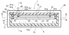
- FIG. 2 is a cross-sectional view taken along line AA in FIG.
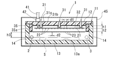
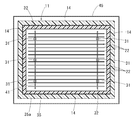
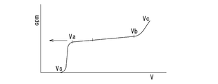
- FIG. 3 is a cross-sectional view taken along the line BB in FIG. 1. It is a graph which shows the relationship between an applied voltage and counting efficiency.
- the ⁇ -ray measuring apparatus 1 of the embodiment includes a box-shaped container 11 having a gas inlet 2 and a gas outlet 3, and an inner surface (ceiling) of the top plate portion 12 of the box-shaped container 11.
- the box-shaped container 11 is formed in a rectangular parallelepiped shape having a bottom plate portion 13, side plate portions 14 surrounding the four sides, and a top plate portion 12.
- the baseplate part 13, each side-plate part 14, and the top-plate part 12 are formed with synthetic resins, such as an acrylic resin.
- a cathode film 21 is formed on the entire inner surface (ceiling surface) of the top plate portion 12 by sputtering or the like.
- a plurality of anode wires 22 are provided in parallel with the cathode film 21.
- a plurality of support rods 31 penetrating both side portions of the top plate portion 12 (cathode film 21) are arranged side by side along the side portion of the top plate portion 12. It has been.
- the support conductors 32 are fixed in parallel to each other along the respective ends of the two rows of support rods 31 (lower ends in FIGS. 1 and 2).
- the support rods 32 are provided in two rows, two support conductors 32 are arranged, one for each row of the support rods.
- An anode wire 22 is provided so as to bridge between the support conducting wires 32.
- each anode wire 22 is held by each supporting conductor 32 by fixing both ends to each supporting conductor 32.
- Each support conducting wire 32 is made of a conductive material having an ⁇ -ray emitting element content of less than 1 ppb, and electrically connects the anode wires 22 to each other.
- Each support bar 31 includes a bar body (inner insulating part) 31 a that penetrates the top plate 12 and the cathode film 21 of the box-shaped container 11, and a portion that penetrates the top plate 12 and is exposed in the box-shaped container 11. It is comprised by the insulation coating part 31b formed so that it might cover.
- the support conducting wire 32 is fixed to the insulating coating portion 31b.
- each support rod 31 includes a rod body 31 a that partially penetrates the hole formed in the cathode membrane 21 and is partially exposed in the box-shaped container 11, and a portion of the rod body 31 a that is exposed in the box-shaped container 11. And an insulating coating 31b for covering.
- the anode wires 22 are provided between the support conductors 32 at the tips of the support rods 31 in parallel to each other along the direction orthogonal to the support conductors 32 and at a constant interval. Are arranged so as to form a parallel plane. Thereby, an electric field of a wide area can be formed.
- the support conducting wire 32 and the anode wire 22 are electrically and mechanically joined by a conductive joining material (not shown) of any one of Ag, Ni, Cu, Al, and Au.
- a conductive joining material (not shown) of any one of Ag, Ni, Cu, Al, and Au.
- the conductive bonding material is specifically formed by applying and solidifying a silver paste made of silver-based powder and resin.
- the joint between the support lead wire 32 and the anode wire 22 is further reinforced by attaching an adhesive such as an epoxy resin.
- an adhesive such as an epoxy resin.
- a structure in which the support conducting wire 32 and the anode wire 22 are directly attached and screwed a structure in which the metal wire is caulked with a metal fitting, or the like may be employed.
- a cable 41 for connecting to an external power source is connected to the anode wire 22 and the cathode film 21.
- the cable 41 is, for example, a coaxial cable, and has an internal conductor 41 a and an external conductor 41 b insulated from the internal conductor 41 a, and is fixed to the top plate portion 12 of the box-shaped container 11 by a connector 42.
- the internal conductor 41 a is electrically connected to the support conductor 32 via the connector 42
- the external conductor 41 b is electrically connected to the cathode film 21 via the connector 42.
- the cathode wire 23 is fixed to a rectangular frame member 35 provided inside the box-shaped container 11.
- the frame member 35 is made of a synthetic resin such as an acrylic resin.
- a conductive film 35 a made of a conductive material is formed on the entire surface of the frame member 35 by sputtering or the like, and the side plate portions 14 are joined to the cathode film 21 of the top plate 12. It is fixed to the inner surface.
- a plurality of cathode wires 23 are provided in parallel to each other at the lower ends of two sides opposed to each other by 180 ° in a state of being bridged therebetween. Since these cathode wires 23 are arranged at the lower end of the frame member 35, these cathode wires 23 are also arranged in a planar shape extending between the lower ends of the frame member 35.
- the cathode wire 23 and the conductive film 35a of the frame member 35 is used for joining the anode wire 22 and the support conducting wire 32. It is electrically and mechanically joined by the same silver-based joining material as that used. Since the cathode wire 23 is bonded to the conductive film 35a of the frame member 35 and the conductive film 35a is bonded to the cathode film 21 of the top plate portion 12, the cathode wire 23 and the cathode film 21 are electrically connected.
- the anode wires 22 are arranged in parallel to the cathode film 21 at a predetermined interval and in parallel to each other, and the cathode wires 23 are also parallel to the surface formed by the anode wires 22. Are arranged in parallel with each other at regular intervals. Each anode wire 22 and each cathode wire 23 are also arranged in parallel to each other.
- the cathode film 21, each anode wire 22, and each cathode wire 23 are all made of a conductive material having a low ⁇ -ray emitting element content.
- a conductive material having a low ⁇ -ray emitting element content For example, copper or aluminum is used as the cathode film 21, and a high purity (5N) tungsten wire is used as the anode wire 22 and the cathode wire 23.
- 5N high purity
- a conductive material is used.
- a high purity (5N) copper wire having a diameter of 1 mm or more and 10 mm or less is used for the support conducting wire 32.
- the thickness of the cathode film 21 is preferably 100 nm or more and 200 nm or less.
- the diameters of the anode wire 22 and the cathode wire 23 are both 30 ⁇ m or less, preferably 1 ⁇ m or more, more preferably 2 ⁇ m or more, and even more preferably 10 ⁇ m or more.
- the distance (interline distance) d1 between the anode wires 22 is preferably 10 mm or more and less than 20 mm, and more preferably 10 mm or more and 19 mm or less.
- the distance (interline distance) d2 between the cathode wires 23 is preferably 5 mm or more and 10 mm or less, and more preferably 5 mm or more and 9 mm or less.
- the plane formed by the anode wire 22 and the cathode film 21 face each other with an area of about 1000 cm 2 . 100 cm 2 or more 1000 cm 2 may be facing in the following areas.
- the distance h1 between the plane formed by the anode wire 22 and the cathode film 21 and the distance h2 between the plane formed by the anode wire 22 and the plane formed by the cathode wire 23 are 3 mm, respectively. It is set to be less than 10 mm and more preferably 3 mm or more and 9 mm or less. In the present embodiment, the separation distance h1 and the separation distance h2 are the same, but may be different.
- FIGS. 1 to 3 are partially exaggerated for convenience of explanation, and do not faithfully reflect actual dimensional relationships.
- Each anode wire 22 and each cathode wire 23 are suspended in a state where a tension of 1 ⁇ 10 ⁇ 2 N or more and 5 ⁇ 10 ⁇ 2 N or less (for example, 4 ⁇ 10 ⁇ 2 N) is applied.
- the upper surface of the bottom plate portion 13 of the box-shaped container 11 serves as a sample holding surface 13a for placing the sample S to be subjected to ⁇ -ray measurement.
- the sample holding surface 13a is arranged below each cathode wire 23 arranged in a plane and in parallel with the surface formed by each cathode wire 23.
- the distance h3 between the upper surface of the sample S placed on the sample holding surface 13a and the cathode wire 23 is set to 1 mm or more and 3 mm or less.
- the sample S is fixed to the sample holding surface 13a by appropriate fixing means as necessary.
- the sample S is, for example, a metal plate, a resin plate, a metal powder, a resin powder, or the like.
- the gas inlet 2 is provided on one side of the two side plate portions 14 facing both ends of the anode wire 22 and the cathode wire 23, and the gas outlet 3 is provided on the other side. ing.
- the gas inlet 2 and the gas outlet 3 are provided in the lower part of the side plate part 14 so as to be separated from the cathode wire 23, and gas flows from one corner of the box-shaped container 11 toward a diagonal corner.
- an acrylic resin having a surface resistivity of 1.0 ⁇ 10 15 ⁇ or more and 1.0 ⁇ 10 16 ⁇ or less is applied to the top plate portion 12, the bottom plate portion 13, the side plate portion 14, and the support rod 31 constituting the box-shaped container 11.
- synthetic resins such as polycarbonate are used.
- the insulating coating part 31b covering the bar body 31a is formed of, for example, an epoxy resin, and an insulating solder resist repair material is applied to the surface thereof.
- a metal case 45 is provided so as to cover the entire box-shaped container 11 and is grounded.
- the sample S to be measured is placed on the sample holding surface 13a of the bottom plate portion 13 in the box-shaped container 11, and argon (Ar) and methane (CH 4 ) are placed.
- a mixed gas is introduced from the gas inlet 2, a high voltage is applied between the cathode membrane 21 and the cathode wire 23 and the anode wire 22 from an external power source, and ⁇ rays emitted from the sample S are generated based on JEDEC STANDARD JESD 221. Can be measured.
- an external power supply it is preferable to use an external power supply with reduced noise.
- noise can be reduced by shielding the internal circuit board of the external power source, installing a filter such as a ferrite core in the power supply unit of the external power source, or adding an earth line of the external power source.
- the gas flow rate is appropriate from 300ml / min to 400ml / min.
- the anode wire 22 and the cathode wire 23 are as thin as 30 ⁇ m or less, ⁇ -ray can be measured without lowering the counting efficiency even at a relatively low voltage.
- FIG. 4 is a graph showing a general relationship between the applied voltage (V) and the counting efficiency (cpm: count / min), and there is a plateau region where the counting efficiency hardly changes even if the voltage changes. Indicates.
- V applied voltage
- cpm count / min
- the voltage is usually applied at the lowest voltage Va in the plateau region.
- the diameters of the anode wire 22 and the cathode wire 23 are reduced to 30 ⁇ m or less.
- a low ⁇ -ray emission amount of 0.001 cph / cm 2 or less can be measured with high reliability in a short time.
- the cathode membrane 21 is disposed on the top plate portion 12 of the box-shaped container 11, the anode wire 22 and the cathode wire 23 are sequentially disposed below the cathode film 21, and the sample holding surface 13 a is disposed on the bottom plate portion 13.
- the cathode membrane 21 may be disposed on the bottom plate portion 13, and the anode wire 22 and the cathode wire 23 may be sequentially disposed above the cathode membrane 21, and the sample holding surface may be formed on the top plate portion 12.
- the support rod 31 that supports the anode wire 22 is provided so as to penetrate the cathode film 21, but it does not necessarily have to penetrate the cathode film 21.
- the support wire 32 may be disposed between the side plate portions 14 of the box-shaped container 11 so that the anode wire 22 is supported by the support wire 32.
- the conductive film 35a covering the entire surface of the frame member 35 that supports the cathode wire 23 is provided and the conductive film 35a is joined to the cathode film 21, but the cathode wire 23 and the cathode film 21 are electrically connected.
- the configuration is not limited to this embodiment as long as the configuration is in the state (the same potential).
- ⁇ -rays were measured under the following various conditions.
- Anode wire 22 diameter ( ⁇ m) -Diameter of cathode wire 23 ( ⁇ m) The separation distance h1 (mm) between the anode wire 22 and the cathode membrane 21 -Distance h2 (mm) between the anode wire 22 and the cathode wire 23 ⁇ Distance between anode wires 22 d1 (mm) -Distance d2 (mm) between cathode wires 23
- the sample S to be measured uses a rolled plate of tin (Sn), and the ⁇ ray emission amount is about 0.001 cph / cm 2 .
- the measurement conditions were a measurement area of 1000 cm 2 , a gas flow rate of 400 ml / min, a counting efficiency of 80% or more, and a measurement time of 100 hours or more.
- Alpha rays can be measured at a lower applied voltage without lowering the counting efficiency, the background can be reduced, and a sample with a low alpha ray emission can be measured in a short time.
Landscapes
- Physics & Mathematics (AREA)
- Health & Medical Sciences (AREA)
- Life Sciences & Earth Sciences (AREA)
- General Physics & Mathematics (AREA)
- High Energy & Nuclear Physics (AREA)
- Molecular Biology (AREA)
- Spectroscopy & Molecular Physics (AREA)
- Measurement Of Radiation (AREA)
- Electron Tubes For Measurement (AREA)
Abstract
ガス流入口及びガス排出口を有する箱型容器と、前記箱型容器の内側に設けられたカソード膜と、該カソード膜と間隔をおいて平行に並べられ、相互に電気的に接続され、直径が1μm以上30μm以下である複数本のアノードワイヤと、前記アノードワイヤと間隔をおいて平行に並べられ、前記カソード膜と電気的に接続され直径が1μm以上30μm以下である複数本のカソードワイヤとを備えるα線測定装置。
Description
本発明は、面状の陰極を用い、ガスを流しながら高電圧を印加してα線を計測する2π型ガスフロー比例計数管に属するα線測定装置に関する。
本願は、2018年4月26日に出願された特願2018-085861号に基づき優先権を主張し、その内容をここに援用する。
本願は、2018年4月26日に出願された特願2018-085861号に基づき優先権を主張し、その内容をここに援用する。
情報機器の高度化に伴い様々な分野に高精度の電子回路が適用されている。この結果、電子回路におけるソフトエラーの発生頻度は、自動車分野においては安全性に、情報通信分野では情報の伝達品質に大きな影響を及ぼす。ソフトエラーの発生頻度を増加させる原因はいくつか存在するが、中でも電子回路を構成する半導体素子を回路基板に接合する接合材から放出されるα線が半導体素子に照射されることで、半導体素子が誤動作することが知られている。このため、実際に半導体素子を回路基板に接合するには、半導体接合材料が所望のα線放出量であることを事前に検証する必要がある。
このα線を計測する装置の一種に、面状の陰極と、線状の陽極及び陰極とを配置した箱型容器内に測定対象試料を配置し、ガスを流しながら陰極と陽極との間に高電圧を印加して、気体の電離作用を利用してα線を計測する2π型ガスフロー比例計数管がある。
例えば、特許文献1に開示の2πガスフロー計数管は、ガス導入出口を有する箱型容器内に、上部より陰極板、多線式陽極、多線式陰極及び試料台が配置された構成とされている。この場合、陰極板、陽極、下部の多線式陰極はいずれもα線放射元素含有量の少ない導電性材料からなる。陰極板には、超高純度の銅、アルミニウム等の金属を蒸着したプラスチック板、超高純度金属メッキ板などが用いられ、陽極としては、線径10~200μmのステンレススチール、銅等の細線が用いられている。
陽極の各細線間の間隔は2~3mm、陽極と各陰極との間隔は1~2cmの範囲に設定される。また、下部の多線式陰極としては、線径50~100μmの陽極と同一材料のものが用いられ、線間隔が5~20mmとすることにより、計数効率が良いと記載されている。試料測定面と下部の多線式陰極との間隔は3~6mmであるとされている。
特許文献1に開示の2πガスフロー計数管を用いたα線測定装置により、各種材料のある程度のα線放出量を計測できる。しかしながら、近年では、α線放出量が極めて少ない半導体接合材料が求められており、このため、例えば、0.001cph/cm2以下の低α線放出量を計測できる装置が求められている。特許文献1開示の装置では、0.001cph/cm2以下の低α線放出量を高い信頼性をもって測定検証することは難しく、測定できるとしても、例えば100時間以上もの測定時間を要する。
本発明は、このような事情に鑑みてなされたもので、例えば0.001cph/cm2以下の低α線放出量を短時間で高い信頼性をもって計測できるα線測定装置を提供することを目的とする。
本発明のα線測定装置は、ガス流入口及びガス排出口を有する箱型容器と、前記箱型容器の内側に設けられたカソード膜と、該カソード膜と間隔をおいて平行にかつ相互に平行に間隔をおいて並べられ、相互に電気的に接続され、直径が30μm以下である複数本のアノードワイヤと、前記アノードワイヤと間隔をおいて平行にかつ相互に平行に間隔をおいて並べられ、前記カソード膜と電気的に接続され、直径が30μm以下である複数本のカソードワイヤとを備える。
α線の計数効率は印加電圧に応じて変化し、印加電圧と放射線の計数効率との関係においては、特定の電圧の範囲で計数効率の変化が少なくほぼ一定となるプラトーと呼ばれる領域が存在する。通常、α線測定時の印加電圧はこのプラトー領域の最低電圧に設定するとよい。一方、微量のα線を短時間で測定するためには、測定装置のバックグランドレベルを低くする必要があるが、このバックグランドレベルを下げるためには、印加電圧を低くする必要がある。しかしながら、プラトー領域の最低電圧からさらに電圧を下げてしまうと、計数効率も低下してしまう。
これに対して、本発明の発明者らは、アノードワイヤの直径及びカソードワイヤの直径をいずれも30μm以下と細くすることによりプラトー領域が低電圧側にシフトすることを発見した。これにより、計数効率を下げることなく、より低い印加電圧にてα線を測定でき、バックグランドも低減し、低α線放出量の試料を短時間で測定することができる。各直径が30μmを超えると、プラトー領域が低電圧側に十分にシフトしないため、バックグランドの影響により低α線放出量の試料を短時間で測定することが難しい。
アノードワイヤの直径及びカソードワイヤの直径の下限値はいずれも好ましくは2μmである。
α線測定装置の一つの実施態様は、前記アノードワイヤと前記カソードワイヤとの直径が同じであることが好ましい。これにより、両極間に形成される電場の間隔が均一になり、計数効率が安定する。
α線測定装置の他の一つの実施態様は、前記カソード膜と前記アノードワイヤとの離間距離、及び前記アノードワイヤと前記カソードワイヤとの離間距離は、いずれも3mm以上10mm未満である。
これらの離間距離が3mm未満では、バックグランドが上昇して低電圧での測定が困難になるおそれがあるとともに、電極間が接近するため測定装置の組み立ても難しくなる。離間距離が10mm以上であると、ノイズが発生し易くなり、それに伴ってバックグランドも上昇するおそれがある。これらアノードワイヤとカソードワイヤとの離間距離は3mm以上9mm以下がより好ましい。
α線測定装置のさらに別の一つの実施態様は、前記アノードワイヤの各線間距離は10mm以上20mm未満であり、前記カソードワイヤの各線間距離は5mm以上10mm以下である。
アノードワイヤについては、各線間距離が10mm未満では電場同士が干渉してバックグラウンドが上昇するおそれがあり、20mm以上であるとアノードワイヤによって形成される電場の間隔が大きくなり、計数効率が低下するおそれがある。計数効率が低下すると、印加電圧を上昇させる必要があるが、その場合、バックグランドが上昇し、目的の性能が出せなくなる。
カソードワイヤも、各線間距離が5mm未満では測定装置のバックグランドが上昇するおそれがあり、10mmを超えると線間が広すぎて計数効率が低下するおそれがある。
アノードワイヤの線間距離は10mm以上19mm以下がより好ましく、カソードワイヤの線間距離は5mm以上9mm以下がより好ましい。
α線測定装置のさらに別の一つの実施態様は、前記箱型容器の内面と各前記アノードワイヤとの間に、絶縁材料からなる複数の支持棒と、α線放射元素の含有量が1ppb未満の導電性材料からなり、各前記アノードワイヤの両端部および各前記支持棒に固定され、前記アノードワイヤを保持するとともに各前記アノードワイヤ同士を電気的に接合する支持導線と、が設けられており、前記支持棒は、前記カソード膜に形成された孔を貫通して前記箱型容器内に一部分が露出する棒状の内側絶縁部と、前記箱型容器内に露出する部分の前記内側絶縁部を覆う絶縁被覆部とを有する。
カソード膜の孔に貫通させる際に内側絶縁部の外周面がカソード膜に接触してカソード膜の一部(粉等)が付着するおそれがあるので、箱形容器内に露出する部分を絶縁被覆部により覆うことにより、絶縁性を高めて支持棒表面での導電性通路(導通経路)の形成を防止し、ノイズを低減している。
α線測定装置のさらに別の一つの実施態様は、各前記アノードワイヤと各前記支持導線との接合部を固定する導電性接合材を備える。
各アノードワイヤが細いので、支持導線との接合部を導電性接合材により接合することで、アノードワイヤの変形、破断等を防止することができ、適切な張力を付与した状態で整然と配置することができる。
α線測定装置のさらに別の一つの実施態様は、前記ガス流入口及びガス排出口は、前記箱型容器の前記カソードワイヤと底面との間の側板部に形成されている。
ガスの流れに伴う箱型容器内の気体の流動がカソードワイヤやアノードワイヤに大きく作用しないようにして、細いアノードワイヤ及びカソードワイヤの振れや撓み等を防止し、測定精度を向上させることができる。
本発明によれば、アノードワイヤ及びカソードワイヤの直径を30μm以下と細くしたので、計数効率を下げることなく、より低い印加電圧にてα線を測定でき、バックグランドも低減し、低α線放出量の試料を短時間で測定することができる。
以下、本発明の実施形態を、図面を参照しながら説明する。実施形態のα線測定装置1は、図1~図3に示すように、ガス流入口2及びガス排出口3を有する箱型容器11と、箱型容器11の天板部12の内面(天井面)に形成されたカソード膜21と、カソード膜21と間隔をおいて平行にかつ相互に平行に間隔をおいて並べられ、相互に電気的に接続された複数本のアノードワイヤ22と、アノードワイヤ22と間隔をおいて平行にかつ相互に平行に間隔をおいて並べられ、カソード膜21と電気的に接続された複数本のカソードワイヤ23とを備えている。
箱型容器11は、底板部13、四方を囲む各側板部14、天板部12を有する直方体状に形成されている。この箱型容器11は、底板部13、各側板部14、天板部12はアクリル樹脂等の合成樹脂により形成されている。天板部12の内面(天井面)には、スパッタリング等によってカソード膜21が全面に形成されている。
このカソード膜21と平行に、複数本のアノードワイヤ22が設けられている。これらアノードワイヤ22を支持するために、天板部12(カソード膜21)の両側部を貫通する複数の支持棒31が、天板部12の側部に沿って2列をなすように並べて設けられている。これら2列の支持棒31の先端(図1,2の下端)に、各列に沿って支持導線32が相互に平行に固着されている。
図3に示すように、支持導線32は、支持棒31が2列に設けられることから、支持棒の列ごとに1本ずつ、合計2本配置されている。この支持導線32間を架け渡すようにアノードワイヤ22が設けられている。
換言すると、箱型容器11の内面と各アノードワイヤ22との間に、絶縁材料からなる複数の支持棒31と、各支持棒31に固定された複数(本実施形態では2本)の支持導線32とが備えられている。各アノードワイヤ22は、両端が各支持導線32に固定されることにより、各支持導線32に保持されている。各支持導線32は、α線放射元素の含有量が1ppb未満の導電性材料からなり、各アノードワイヤ22同士を電気的に接続している。
各支持棒31は、箱型容器11の天板部12およびカソード膜21を貫通する棒本体(内側絶縁部)31aと、天板部12を貫通して箱型容器11内に露出する部分を覆うように形成された絶縁被覆部31bとにより構成される。支持導線32は、その絶縁被覆部31bに固定される。
換言すると、各支持棒31は、カソード膜21に形成された孔を貫通して箱形容器11内に一部分が露出する棒本体31aと、箱型容器11内に露出する部分の棒本体31aを覆う絶縁被覆部31bとを有する。棒本体31aが絶縁被覆部31bによって覆われることにより、棒本体31aが貫通しているカソード膜21と絶縁被覆部31bに固定されている各支持導線32とが確実に絶縁される。
各アノードワイヤ22は、これら支持棒31先端の支持導線32の間に、支持導線32に直交する方向に沿って相互に平行に、かつ一定間隔で設けられることにより、カソード膜21と一定の間隔をおく平行な面状をなすように配置される。これにより、広い面積の電場を形成できる。
支持導線32とアノードワイヤ22との間は、Ag、Ni,Cu,Al,Auのいずれかの系の導電性接合材(図示略)によって電気的、機械的に接合されている。導電性接合材は、例えば、銀系接合材の場合には、具体的には、銀系粉末と樹脂等からなる銀ペーストを塗布して固化することにより形成される。支持導線32とアノードワイヤ22との接合部は、さらにエポキシ樹脂等の接着剤を付着させて補強される。なお、支持導線32とアノードワイヤ22との接合は、直接くくりつけてねじ止めする構造や、金具でかしめる構造等を採用してもよい。
図2,3に示すように、これらアノードワイヤ22及びカソード膜21に、外部の電源(図示略)と接続するためのケーブル41が接続されている。ケーブル41は例えば同軸ケーブルであり、内部導線41aと、内部導線41aから絶縁された外部導線41bとを有し、箱型容器11の天板部12にコネクタ42によって固定される。内部導線41aはコネクタ42を介して支持導線32に電気的に接続され、外部導線41bはコネクタ42を介してカソード膜21に電気的に接続される。
カソードワイヤ23は、箱型容器11の内側に設けた矩形の枠部材35に固定されている。枠部材35は、アクリル樹脂等の合成樹脂からなり、その表面の全面にスパッタリング等によって導電材料からなる導電膜35aが形成され、天板部12のカソード膜21に接合した状態で各側板部14の内面に固定されている。この枠部材35において180°対向する二辺の下端に、これらの間に架け渡された状態で複数本のカソードワイヤ23が相互に平行に設けられている。これらカソードワイヤ23が枠部材35の下端に並べられるため、これらカソードワイヤ23も枠部材35の下端間にまたがる面状に配置される。
これらカソードワイヤ23と枠部材35の導電膜35aとの間、及び枠部材35の導電膜35aと天板部12のカソード膜21との間は、アノードワイヤ22と支持導線32との接合に用いたものと同様の銀系接合材によって電気的、機械的に接合されている。カソードワイヤ23が枠部材35の導電膜35aに接合され、導電膜35aが天板部12のカソード膜21に接合しているので、カソードワイヤ23とカソード膜21とは電気的に接続される。
前述したように、各アノードワイヤ22はカソード膜21に対して平行に一定の間隔をおいてかつ相互に平行に配置され、各カソードワイヤ23も各アノードワイヤ22により形成される面に対して平行に一定の間隔をおいてかつ相互に平行に配置される。各アノードワイヤ22と各カソードワイヤ23とも相互に平行に配置される。
カソード膜21、各アノードワイヤ22及び各カソードワイヤ23は、いずれもα線放射元素含有量の少ない導電材料からなる。例えば、カソード膜21としては銅又はアルミニウムが用いられ、アノードワイヤ22及びカソードワイヤ23としては高純度(5N)のタングステン線が用いられる。例えばタングステン線を使用する場合、強度が高いので直径10μm以下でも切れにくい。
支持導線32や枠部材35表面の導電膜35aも、ウラン、トリウム、鉛等のα線放射元素の含有量が合計で1ppb未満である銅、銅合金、アルミニウム、、アルミニウム合金、タングステン、タングステン合金といった導電材料が用いられる。例えば、支持導線32は直径1mm以上10mm以下の高純度(5N)の銅線が用いられる。
カソード膜21の厚みは100nm以上200nm以下が好ましい。アノードワイヤ22及びカソードワイヤ23の直径はいずれも30μm以下であり、好ましくは1μm以上、より好ましくは2μm以上、さらに好ましくは10μm以上である。アノードワイヤ22どうしの間隔(線間距離)d1は10mm以上20mm未満が好ましく、10mm以上19mm以下がより好ましい。カソードワイヤ23どうしの間隔(線間距離)d2は5mm以上10mm以下が好ましく、5mm以上9mm以下がより好ましい。
アノードワイヤ22により形成される平面とカソード膜21とは、約1000cm2の面積で対向する。100cm2以上1000cm2以下の面積で対向するとよい。これらアノードワイヤ22により形成される平面とカソード膜21との離間距離h1、及び、アノードワイヤ22により形成される平面とカソードワイヤ23により形成される平面との面間の離間距離h2は、それぞれ3mm以上10mm未満に設定され、3mm以上9mm以下がより好ましい。本実施形態では離間距離h1と離間距離h2とは同一であるが、異なっていてもよい。
なお、図1~図3は、説明の便宜のため、部分的に誇張した寸法関係に設定しており、実際の寸法関係を忠実に反映したものではない。
各アノードワイヤ22及び各カソードワイヤ23は、それぞれ1×10⁻²N以上5×10⁻²N以下(例えば4×10⁻²N)の張力が付与された状態に懸架される。
箱型容器11の底板部13の上面は、α線測定対象となる試料Sを載置するための試料保持面13aとなっている。試料保持面13aは、面状に配置されている各カソードワイヤ23の下方に、各カソードワイヤ23が構成する面と平行に配置される。この試料保持面13aに載置される試料Sの上面とカソードワイヤ23との離間距離h3は、1mm以上3mm以下に設定される。試料Sは、必要に応じて適宜の固定手段によって試料保持面13aに固定される。試料Sは、例えば、金属板や樹脂板、金属粉末や樹脂粉末等である。
箱型容器11の4つの側板部14のうち、アノードワイヤ22やカソードワイヤ23の両端が対向している2つの側板部14の一方にガス流入口2、他方にガス排出口3がそれぞれ設けられている。ガス流入口2とガス排出口3は、カソードワイヤ23から離間するように側板部14の下部に設けられ、箱型容器11の1つの隅部から対角上の隅部に向けてガスが流れるように配置されている。ガス流入口2とガス排出口3を上述のように設けることで、ガスの流入に伴う箱型容器11内の気体の流動が、カソードワイヤ23やアノードワイヤ22に大きく作用しないようにして、細いアノードワイヤ22及びカソードワイヤ23の振れや撓み等を防止し、測定精度を向上させることができる。
箱型容器11を構成する天板部12、底板部13、側板部14、および支持棒31には、表面抵抗率が1.0×10¹⁵Ω以上1.0×10¹⁶Ω以下のアクリル樹脂やポリカーボネート等の合成樹脂が用いられる。支持棒31において、棒本体31aを覆う絶縁被覆部31bは例えばエポキシ樹脂により形成され、その表面に絶縁性のソルダーレジスト補修材が塗布される。
箱型容器11の全体を覆うように金属ケース45が設けられ、アース接続される。
このように構成されたα線測定装置1を用いて、箱型容器11における底板部13の試料保持面13aに測定対象の試料Sを載置し、アルゴン(Ar)とメタン(CH4)の混合ガスをガス流入口2から流入させ、カソード膜21及びカソードワイヤ23とアノードワイヤ22との間に外部電源から高電圧を印加し、JEDEC STANDARD JESD221に基づき、試料Sから放出されるα線を測定することができる。
外部電源としては、ノイズが低減された外部電源を用いることが好ましい。例えば、外部電源の内部回路基板にシールドを施したり、外部電源の電力供給部へフェライトコアなどのフィルタを設置したり、外部電源のアースラインを増設するなどしてノイズを低減させることができる。
ガスの流量は300ml/分以上400ml/分以下が適切である。
この実施形態のα線測定装置1においては、アノードワイヤ22及びカソードワイヤ23が30μm以下と細いため、比較的低い電圧であっても、計数効率を下げることなくα線を測定することができる。
図4は、印加電圧(V)と計数効率(cpm:count/min)との一般的な関係を示すグラフであり、電圧の変化があっても計数効率がほとんど変化しないプラトー領域が存在することを示す。α線測定においては、通常、このプラトー領域における最低電圧Vaで印加されるが、本実施形態のα線測定装置1においては、アノードワイヤ22及びカソードワイヤ23の直径を30μm以下と細くしたことにより、図4の矢印で示すようにプラトー領域を全体に低電圧側にシフトさせる効果がある。これにより、低い電圧でも計数効率を低下させることなくα線を測定することができる。
したがって、例えば0.001cph/cm2以下の低α線放出量を、短時間で高い信頼性をもって計測することができる。
なお、本発明は上記実施形態に限るものではない。例えば、上記実施形態では、箱型容器11の天板部12にカソード膜21、その下方にアノードワイヤ22、カソードワイヤ23を順次配置し、底板部13に試料保持面13aを配置した。逆に、底板部13にカソード膜21、その上方にアノードワイヤ22、カソードワイヤ23を順次配置し、天板部12に試料保持面を形成してもよい。
上記実施形態ではアノードワイヤ22を支持する支持棒31を、カソード膜21を貫通するように設けたが、必ずしもカソード膜21を貫通していなくてもよい。例えば、箱型容器11の側板部14間に支持導線32を架け渡すように配置し、その支持導線32にアノードワイヤ22を支持させてもよい。
上記実施形態ではカソードワイヤ23を支持する枠部材35の全面を覆う導電膜35aを設けて、導電膜35aをカソード膜21に接合させたが、カソードワイヤ23とカソード膜21とが電気的に接続状態(同電位)となる構成であれば、この実施形態に限らない。
上記実施形態にて説明した部品構成のα線測定装置1を用いて、以下の諸条件を変えてそれぞれα線を測定した。
・アノードワイヤ22の直径(μm)
・カソードワイヤ23の直径(μm)
・アノードワイヤ22とカソード膜21との離間距離h1(mm)
・アノードワイヤ22とカソードワイヤ23との離間距離h2(mm)
・アノードワイヤ22の線間距離d1(mm)
・カソードワイヤ23の線間距離d2(mm)
・カソードワイヤ23の直径(μm)
・アノードワイヤ22とカソード膜21との離間距離h1(mm)
・アノードワイヤ22とカソードワイヤ23との離間距離h2(mm)
・アノードワイヤ22の線間距離d1(mm)
・カソードワイヤ23の線間距離d2(mm)
測定対象の試料Sは、錫(Sn)の圧延板を用い、α線放出量が0.001cph/cm2程度である。
測定条件については、測定面積1000cm2、ガス流量400ml/min、計数効率80%以上、測定時間100時間以上で実施した。
α線測定装置のバックグランド値と、0.001cph/cm2を測定するために要する印加電圧(Va)、測定時間を計測した。その結果を表1に示す。

表1に示されるように、アノードワイヤ及びカソードワイヤの直径がいずれも30μm以下の場合に、バックグランド値が低く、0.001cph/cm2を測定に要する時間も短かった。特に、ワイヤ直径がいずれも10μmである実験3では測定に要した時間が短く、50時間以内であった。
計数効率を下げることなく、より低い印加電圧にてα線を測定でき、バックグランドも低減し、低α線放出量の試料を短時間で測定できる。
1 α線測定装置
2 ガス流入口
3 ガス排出口
11 箱型容器
12 天板部
13 底板部
13a 試料保持面
14 側板部
21 カソード膜
22 アノードワイヤ
23 カソードワイヤ
31 支持棒
31a 棒本体(内側絶縁部)
31b 絶縁被覆部
32 支持導線
35 枠部材
35a 導電膜
41 ケーブル
41a 内部導線
41b 外部導線
42 コネクタ
45 金属ケース
S 試料
2 ガス流入口
3 ガス排出口
11 箱型容器
12 天板部
13 底板部
13a 試料保持面
14 側板部
21 カソード膜
22 アノードワイヤ
23 カソードワイヤ
31 支持棒
31a 棒本体(内側絶縁部)
31b 絶縁被覆部
32 支持導線
35 枠部材
35a 導電膜
41 ケーブル
41a 内部導線
41b 外部導線
42 コネクタ
45 金属ケース
S 試料
Claims (16)
- ガス流入口及びガス排出口を有する箱型容器と、
前記箱型容器の内側に設けられたカソード膜と、
前記カソード膜と間隔をおいて平行にかつ相互に平行に間隔をおいて並べられ、相互に電気的に接続され、直径が30μm以下である複数本のアノードワイヤと、
前記アノードワイヤと間隔をおいて平行にかつ相互に平行に間隔をおいて並べられ、前記カソード膜と電気的に接続され、直径が30μm以下である複数本のカソードワイヤと
を備えることを特徴とするα線測定装置。 - 前記アノードワイヤの前記直径および前記カソードワイヤの前記直径がいずれも2μm以上であることを特徴とする請求項1に記載のα線測定装置。
- 前記アノードワイヤの前記直径と前記カソードワイヤとの前記直径が同じであることを特徴とする請求項1または2のいずれか記載のα線測定装置。
- 前記カソード膜と前記アノードワイヤとの離間距離、及び前記アノードワイヤと前記カソードワイヤとの離間距離は、いずれも3mm以上10mm未満であることを特徴とする請求項1から3のいずれか一項に記載のα線測定装置。
- 前記カソード膜と前記アノードワイヤとの前記離間距離、及び前記アノードワイヤと前記カソードワイヤとの前記離間距離は、いずれも9mm以下であることを特徴とする請求項4記載のα線測定装置。
- 前記アノードワイヤの各線間距離は10mm以上20mm未満であり、前記カソードワイヤの各線間距離は5mm以上10mm以下であることを特徴とする請求項1から5のいずれか一項記載のα線測定装置。
- 前記アノードワイヤの前記線間距離が19mm以下であることを特徴とする請求項6記載のα線測定装置。
- 前記カソードワイヤの前記線間距離が9mm以下であることを特徴とする請求項6記載のα線測定装置。
- 前記箱型容器の内面と各前記アノードワイヤとの間に、絶縁材料からなる複数の支持棒と、α線放射元素の含有量が1ppb未満の導電性材料からなり、各前記アノードワイヤの両端部および各前記支持棒に固定され、前記アノードワイヤを保持するとともに各前記アノードワイヤ同士を電気的に接続する複数の支持導線と、が設けられており、
前記支持棒は、前記カソード膜に形成された孔を貫通して前記箱形容器内に一部分が露出する棒状の内側絶縁部と、前記箱型容器内に露出する部分の前記内側絶縁部を覆う絶縁被覆部とを有する
ことを特徴とする請求項1から8のいずれか一項記載のα線測定装置。 - 各前記アノードワイヤと各前記支持導線との接合部を固定する導電性接合材を備えることを特徴とする請求項9記載のα線測定装置。
- 前記支持導線は直径1mm以上10mm以下の銅線であることを特徴とする請求項9記載のα線測定装置。
- 前記ガス流入口及び前記ガス排出口は、前記箱型容器の前記カソードワイヤと底面との間の側板部に形成されていることを特徴とする請求項1から11のいずれか一項記載のα線測定装置。
- 前記カソード膜は銅又はアルミニウムからなることを特徴とする請求項1から12のいずれか一項記載のα線測定装置。
- 前記カソード膜の厚さは100nm以上200nm以下であることを特徴とする請求項1から13のいずれか一項記載のα線測定装置。
- 前記アノードワイヤおよび前記カソードワイヤはタングステン線であることを特徴とする請求項1から14のいずれか一項記載のα線測定装置。
- 各前記アノードワイヤにより形成される平面とカソード膜とは100cm2以上1000cm2以下の面積で対向することを特徴とする請求項1から15のいずれか一項記載のα線測定装置。
Priority Applications (2)
| Application Number | Priority Date | Filing Date | Title |
|---|---|---|---|
| CN201980027258.1A CN112041703B (zh) | 2018-04-26 | 2019-04-22 | α射线测定装置 |
| US17/049,404 US10996346B2 (en) | 2018-04-26 | 2019-04-22 | α-ray measuring device |
Applications Claiming Priority (2)
| Application Number | Priority Date | Filing Date | Title |
|---|---|---|---|
| JP2018085861 | 2018-04-26 | ||
| JP2018-085861 | 2018-04-26 |
Publications (1)
| Publication Number | Publication Date |
|---|---|
| WO2019208477A1 true WO2019208477A1 (ja) | 2019-10-31 |
Family
ID=68294528
Family Applications (1)
| Application Number | Title | Priority Date | Filing Date |
|---|---|---|---|
| PCT/JP2019/016962 Ceased WO2019208477A1 (ja) | 2018-04-26 | 2019-04-22 | α線測定装置 |
Country Status (5)
| Country | Link |
|---|---|
| US (1) | US10996346B2 (ja) |
| JP (1) | JP6604453B2 (ja) |
| CN (1) | CN112041703B (ja) |
| TW (1) | TWI736879B (ja) |
| WO (1) | WO2019208477A1 (ja) |
Families Citing this family (4)
| Publication number | Priority date | Publication date | Assignee | Title |
|---|---|---|---|---|
| WO2021079957A1 (ja) | 2019-10-25 | 2021-04-29 | 京セラ株式会社 | 取引支援システム及び取引支援方法 |
| CN113219511A (zh) * | 2021-06-02 | 2021-08-06 | 山西中辐核仪器有限责任公司 | 一种精准寻找表面辐射污染位置的探测方法和探测器 |
| CN113568031B (zh) * | 2021-06-11 | 2023-11-03 | 中国电子产品可靠性与环境试验研究所((工业和信息化部电子第五研究所)(中国赛宝实验室)) | α粒子发射率测试方法 |
| CN119439224B (zh) * | 2024-12-10 | 2025-12-30 | 深圳市计量质量检测研究院 | α粒子测量设备、方法、装置、存储介质和程序产品 |
Citations (5)
| Publication number | Priority date | Publication date | Assignee | Title |
|---|---|---|---|---|
| JPS6154489A (ja) * | 1984-08-24 | 1986-03-18 | Sumitomo Alum Smelt Co Ltd | 大面積線源用多線式2πガスフロ−計数管 |
| JPS63238587A (ja) * | 1987-03-27 | 1988-10-04 | ベ−タジエン・コ−ポレ−シヨン | 荷電粒子を放出する放射性核種の表面分布を測定する方法及び装置 |
| JPH01211852A (ja) * | 1987-10-17 | 1989-08-25 | Lab Prof Dr Rudolf Berthold Gmbh & Co | 電離放射線を位置的に高感度に測定する二次元比例計数管 |
| US5019711A (en) * | 1989-03-21 | 1991-05-28 | The Regents Of The University Of Michigan | Scanning-liquid ionization chamber imager/dosimeter for megavoltage photons |
| JPH0541196A (ja) * | 1991-08-02 | 1993-02-19 | Mitsubishi Electric Corp | 荷電粒子ビームモニタ |
Family Cites Families (11)
| Publication number | Priority date | Publication date | Assignee | Title |
|---|---|---|---|---|
| US4264816A (en) * | 1979-11-29 | 1981-04-28 | The United States Of America As Represented By The United States Department Of Energy | Ionization chamber |
| US5138168A (en) * | 1988-07-08 | 1992-08-11 | Oxford Positron Systems Limited | Method and apparatus for quantitative autoradiography analysis |
| US20050194541A1 (en) * | 2004-03-03 | 2005-09-08 | Clark Brett M. | Large area ionization detector and methods for detecting low level radiation |
| CN200982957Y (zh) * | 2006-11-30 | 2007-11-28 | 中国辐射防护研究院 | 流气式正比探测器阵列 |
| JP5855577B2 (ja) | 2010-12-01 | 2016-02-09 | Hoya株式会社 | 電子増幅器用基板の製造方法、電子増幅器の製造方法及び放射線検出器の製造方法 |
| CN103380194A (zh) | 2011-01-31 | 2013-10-30 | 古河机械金属株式会社 | 闪烁体用石榴石型晶体和使用该石榴石型晶体的放射线检测器 |
| US9217793B2 (en) * | 2012-10-25 | 2015-12-22 | Schlumberger Technology Corporation | Apparatus and method for detecting radiation |
| CN103926615B (zh) * | 2014-04-23 | 2016-05-04 | 中国原子能科学研究院 | 2π多丝流气式正比计数器 |
| JP6638226B2 (ja) | 2015-07-09 | 2020-01-29 | 富士電機株式会社 | 放射線モニタ及びハンドフットクロスモニタ |
| CN105629285B (zh) * | 2016-01-19 | 2018-05-18 | 中国计量科学研究院 | 一种多丝正比计数器 |
| CN207717993U (zh) * | 2017-12-19 | 2018-08-10 | 北京中合宏信科技有限公司 | 流气式放射源活度测量装置 |
-
2019
- 2019-04-22 CN CN201980027258.1A patent/CN112041703B/zh active Active
- 2019-04-22 US US17/049,404 patent/US10996346B2/en active Active
- 2019-04-22 WO PCT/JP2019/016962 patent/WO2019208477A1/ja not_active Ceased
- 2019-04-22 JP JP2019080753A patent/JP6604453B2/ja not_active Expired - Fee Related
- 2019-04-24 TW TW108114258A patent/TWI736879B/zh active
Patent Citations (5)
| Publication number | Priority date | Publication date | Assignee | Title |
|---|---|---|---|---|
| JPS6154489A (ja) * | 1984-08-24 | 1986-03-18 | Sumitomo Alum Smelt Co Ltd | 大面積線源用多線式2πガスフロ−計数管 |
| JPS63238587A (ja) * | 1987-03-27 | 1988-10-04 | ベ−タジエン・コ−ポレ−シヨン | 荷電粒子を放出する放射性核種の表面分布を測定する方法及び装置 |
| JPH01211852A (ja) * | 1987-10-17 | 1989-08-25 | Lab Prof Dr Rudolf Berthold Gmbh & Co | 電離放射線を位置的に高感度に測定する二次元比例計数管 |
| US5019711A (en) * | 1989-03-21 | 1991-05-28 | The Regents Of The University Of Michigan | Scanning-liquid ionization chamber imager/dosimeter for megavoltage photons |
| JPH0541196A (ja) * | 1991-08-02 | 1993-02-19 | Mitsubishi Electric Corp | 荷電粒子ビームモニタ |
Also Published As
| Publication number | Publication date |
|---|---|
| CN112041703B (zh) | 2022-05-17 |
| TW201945753A (zh) | 2019-12-01 |
| US20210055430A1 (en) | 2021-02-25 |
| JP6604453B2 (ja) | 2019-11-13 |
| US10996346B2 (en) | 2021-05-04 |
| JP2019194579A (ja) | 2019-11-07 |
| TWI736879B (zh) | 2021-08-21 |
| CN112041703A (zh) | 2020-12-04 |
Similar Documents
| Publication | Publication Date | Title |
|---|---|---|
| JP6604453B2 (ja) | α線測定装置 | |
| US6418009B1 (en) | Broadband multi-layer capacitor | |
| US9176170B2 (en) | Current sensor | |
| US11476172B2 (en) | Radio frequency module | |
| CN111564278B (zh) | 层叠线圈部件 | |
| US20200051717A1 (en) | Current sensing resistor | |
| CN104520944B (zh) | 电阻器特别是低电阻电流测量电阻器 | |
| CN105825994A (zh) | 电子组件 | |
| US12146899B2 (en) | Current detection resistor and current detection apparatus | |
| CN105825995B (zh) | 电子组件 | |
| US8659912B2 (en) | Shielding device for shielding an electronic component | |
| JP6256819B2 (ja) | 電流センサ及び電流測定装置 | |
| US8928137B2 (en) | Flow meter with ultrasound transducer directly connected to and fixed to measurement circuit board | |
| US10454445B2 (en) | Common mode filter | |
| JPWO2010117058A1 (ja) | コンタクトプローブおよびプローブユニット | |
| JP7290512B2 (ja) | 電磁流量計 | |
| US20210225563A1 (en) | Shunt resistor and shunt resistor mounting structure | |
| KR100811740B1 (ko) | 프로브 니들용 튜브 및 그 제조 방법 | |
| CA3118576C (en) | Electricity meter | |
| CN103235251B (zh) | 一种极低温下半导体量子点低噪测量系统 | |
| CN110764032B (zh) | 用于光泵磁力仪的射频薄膜 | |
| JP5654793B2 (ja) | 放射線検出素子、及び放射線検出素子の製造方法 | |
| KR200465556Y1 (ko) | 알루미늄 권선 인덕터 | |
| KR101037770B1 (ko) | 스퀴드 센서 및 그 제조방법 | |
| JP4449955B2 (ja) | 表面実装用電子部品のインピーダンス測定方法 |
Legal Events
| Date | Code | Title | Description |
|---|---|---|---|
| 121 | Ep: the epo has been informed by wipo that ep was designated in this application |
Ref document number: 19793374 Country of ref document: EP Kind code of ref document: A1 |
|
| NENP | Non-entry into the national phase |
Ref country code: DE |
|
| 122 | Ep: pct application non-entry in european phase |
Ref document number: 19793374 Country of ref document: EP Kind code of ref document: A1 |