WO2019207668A1 - 荷電粒子線装置の照射条件決定方法、及び荷電粒線装置 - Google Patents
荷電粒子線装置の照射条件決定方法、及び荷電粒線装置 Download PDFInfo
- Publication number
- WO2019207668A1 WO2019207668A1 PCT/JP2018/016741 JP2018016741W WO2019207668A1 WO 2019207668 A1 WO2019207668 A1 WO 2019207668A1 JP 2018016741 W JP2018016741 W JP 2018016741W WO 2019207668 A1 WO2019207668 A1 WO 2019207668A1
- Authority
- WO
- WIPO (PCT)
- Prior art keywords
- irradiation points
- irradiation
- distance
- points
- charged particle
- Prior art date
- Legal status (The legal status is an assumption and is not a legal conclusion. Google has not performed a legal analysis and makes no representation as to the accuracy of the status listed.)
- Ceased
Links
Images










Classifications
-
- H—ELECTRICITY
- H01—ELECTRIC ELEMENTS
- H01J—ELECTRIC DISCHARGE TUBES OR DISCHARGE LAMPS
- H01J37/00—Discharge tubes with provision for introducing objects or material to be exposed to the discharge, e.g. for the purpose of examination or processing thereof
- H01J37/02—Details
- H01J37/22—Optical, image processing or photographic arrangements associated with the tube
- H01J37/222—Image processing arrangements associated with the tube
-
- H—ELECTRICITY
- H01—ELECTRIC ELEMENTS
- H01J—ELECTRIC DISCHARGE TUBES OR DISCHARGE LAMPS
- H01J37/00—Discharge tubes with provision for introducing objects or material to be exposed to the discharge, e.g. for the purpose of examination or processing thereof
- H01J37/02—Details
- H01J37/22—Optical, image processing or photographic arrangements associated with the tube
-
- H—ELECTRICITY
- H01—ELECTRIC ELEMENTS
- H01J—ELECTRIC DISCHARGE TUBES OR DISCHARGE LAMPS
- H01J37/00—Discharge tubes with provision for introducing objects or material to be exposed to the discharge, e.g. for the purpose of examination or processing thereof
- H01J37/26—Electron or ion microscopes; Electron or ion diffraction tubes
- H01J37/28—Electron or ion microscopes; Electron or ion diffraction tubes with scanning beams
-
- H—ELECTRICITY
- H01—ELECTRIC ELEMENTS
- H01J—ELECTRIC DISCHARGE TUBES OR DISCHARGE LAMPS
- H01J37/00—Discharge tubes with provision for introducing objects or material to be exposed to the discharge, e.g. for the purpose of examination or processing thereof
- H01J37/02—Details
- H01J37/04—Arrangements of electrodes and associated parts for generating or controlling the discharge, e.g. electron-optical arrangement or ion-optical arrangement
- H01J37/147—Arrangements for directing or deflecting the discharge along a desired path
- H01J37/1472—Deflecting along given lines
- H01J37/1474—Scanning means
-
- H—ELECTRICITY
- H01—ELECTRIC ELEMENTS
- H01J—ELECTRIC DISCHARGE TUBES OR DISCHARGE LAMPS
- H01J37/00—Discharge tubes with provision for introducing objects or material to be exposed to the discharge, e.g. for the purpose of examination or processing thereof
- H01J37/02—Details
- H01J37/244—Detectors; Associated components or circuits therefor
-
- H—ELECTRICITY
- H01—ELECTRIC ELEMENTS
- H01J—ELECTRIC DISCHARGE TUBES OR DISCHARGE LAMPS
- H01J2237/00—Discharge tubes exposing object to beam, e.g. for analysis treatment, etching, imaging
- H01J2237/04—Means for controlling the discharge
- H01J2237/043—Beam blanking
- H01J2237/0432—High speed and short duration
-
- H—ELECTRICITY
- H01—ELECTRIC ELEMENTS
- H01J—ELECTRIC DISCHARGE TUBES OR DISCHARGE LAMPS
- H01J2237/00—Discharge tubes exposing object to beam, e.g. for analysis treatment, etching, imaging
- H01J2237/245—Detection characterised by the variable being measured
- H01J2237/24564—Measurements of electric or magnetic variables, e.g. voltage, current, frequency
-
- H—ELECTRICITY
- H01—ELECTRIC ELEMENTS
- H01J—ELECTRIC DISCHARGE TUBES OR DISCHARGE LAMPS
- H01J2237/00—Discharge tubes exposing object to beam, e.g. for analysis treatment, etching, imaging
- H01J2237/245—Detection characterised by the variable being measured
- H01J2237/24571—Measurements of non-electric or non-magnetic variables
- H01J2237/24578—Spatial variables, e.g. position, distance
-
- H—ELECTRICITY
- H01—ELECTRIC ELEMENTS
- H01J—ELECTRIC DISCHARGE TUBES OR DISCHARGE LAMPS
- H01J2237/00—Discharge tubes exposing object to beam, e.g. for analysis treatment, etching, imaging
- H01J2237/26—Electron or ion microscopes
- H01J2237/28—Scanning microscopes
- H01J2237/2801—Details
-
- H—ELECTRICITY
- H01—ELECTRIC ELEMENTS
- H01J—ELECTRIC DISCHARGE TUBES OR DISCHARGE LAMPS
- H01J2237/00—Discharge tubes exposing object to beam, e.g. for analysis treatment, etching, imaging
- H01J2237/26—Electron or ion microscopes
- H01J2237/28—Scanning microscopes
- H01J2237/2803—Scanning microscopes characterised by the imaging method
-
- H—ELECTRICITY
- H01—ELECTRIC ELEMENTS
- H01J—ELECTRIC DISCHARGE TUBES OR DISCHARGE LAMPS
- H01J2237/00—Discharge tubes exposing object to beam, e.g. for analysis treatment, etching, imaging
- H01J2237/26—Electron or ion microscopes
- H01J2237/282—Determination of microscope properties
- H01J2237/2826—Calibration
Definitions
- the present disclosure relates to a charged particle beam apparatus that irradiates a sample with a charged particle beam, and more particularly, to a charged particle beam apparatus that irradiates a charged particle beam in a pulsed manner.
- Patent Document 1 discloses an apparatus that controls the scanning speed and irradiation interval of an electron beam, controls the amount of charge applied to the sample, suppresses the potential contrast, and maximizes the contrast of the region desired to be observed on the sample. Is disclosed. Patent Documents 2 and 3 disclose electron microscopes that can irradiate a pulsed electron beam and adjust the pulse width of the pulse beam and the interval time between pulses.
- a beam irradiation condition determination method for performing beam scanning while irradiating a beam in a pulse shape, wherein the irradiation point is changed by changing a distance between irradiation points of the pulsed beam.
- Acquire multiple images with different distances evaluate the feature values of specific areas of the images with different distances between the irradiation points, and specify the distance between the irradiation points of the beams so that the feature values are in a predetermined state
- the distance between the specified irradiation points is set, or a plurality of distances between the irradiation points determined based on the distance between the specified irradiation points is set, and the distance between the specified irradiation points or the plurality of irradiations is set.
- the apparatus has a scanning deflector that scans a beam, and a beam column that irradiates the sample with a beam scanned by the scanning deflector in a pulsed manner.
- a detector for detecting particles obtained by beam irradiation and a control system for controlling the beam column are provided, and the control system processes the output of the detector to acquire one or more image feature quantities.
- the control system is configured to determine a distance between irradiation points of the pulsed beam such that a feature amount of one or more specific regions of an image obtained based on the output of the detector is in a predetermined state.
- a state in which the specified distance between the irradiation points is specified or a plurality of distances between the irradiation points determined based on the specified distance between the irradiation points is set Then, the time between the irradiation points of the pulsed beam is changed, and the beam irradiation is performed at the time between the irradiation points where the feature amounts of the plurality of specific regions of the image obtained based on the output of the detector are in a predetermined state.
- a charged particle beam device configured to direct is proposed.
- FIG. 3 shows a cross-sectional structure of the sample of Example 1.
- FIG. 6 is a diagram showing a cross-sectional structure of a sample of Example 3.
- the graph which shows the relationship between the distance between irradiation points of a pulse beam, and the luminance value of ROI.
- the graph which shows the relationship between the time between irradiation points of a pulse beam, and the brightness
- FIG. 5 is a diagram showing a cross-sectional structure of a sample of Example 4.
- the figure which shows an example of a scanning electron microscope image.
- the graph which shows the relationship between the distance between irradiation points of a pulse beam, and the luminance value of ROI.
- the figure which shows a mode that the brightness
- the flowchart which shows the process of determining the irradiation condition of a beam.
- the figure which shows an example of the GUI screen which inputs the irradiation conditions of a beam.
- FIG. 5 is a diagram showing a cross-sectional structure of a sample of Example 4.
- the figure which shows an example of a scanning electron microscope image.
- the graph which shows the relationship between the distance between irradiation points of a pulse beam, and the luminance value of ROI.
- the figure which shows a mode that
- FIG. 6 shows a cross-sectional structure of a sample of Example 5.
- the figure which shows an example of a scanning electron microscope image.
- the graph which shows the relationship between the irradiation charge amount of a beam, and a luminance value.
- the flowchart which shows the process of determining automatically ROI of observation object.
- the figure which shows an example of the GUI screen for inputting the kind of sample, and the coordinate of ROI used as observation object.
- a scanning electron microscope that scans an electron beam with respect to a sample is an apparatus that can obtain a high-resolution image.
- a scanning electron microscope focuses and scans an electron beam emitted from an electron source by applying an electromagnetic field on the sample, and detects and images the electrons emitted from the sample when the electron beam is irradiated with a detector. It is a device to do. Since the number of detected electrons reflects the information of the sample, an image with contrast can be formed by scanning the electron beam.
- the contrast of the image is roughly classified into a shape contrast reflecting the sample shape information, a material contrast reflecting the composition information, and a potential contrast reflecting the surface potential information.
- a shape contrast reflecting the sample shape information a shape contrast reflecting the sample shape information
- a material contrast reflecting the composition information a material contrast reflecting the composition information
- a potential contrast reflecting the surface potential information In the scanning electron microscope, information for analyzing shape contrast and material contrast can be obtained.
- a so-called image defect such as a loss of shape contrast may occur due to charge accumulated in the sample. This is because the potential contrast is superimposed on the shape contrast. If the potential contrast is suppressed, an image that reflects the shape contrast relatively strongly can be acquired.
- a potential contrast image can be generated for a region (Region Of Interest: ROI) to be observed on the sample
- the internal structure of the sample can be observed.
- ROI Region Of Interest
- the potential contrast is observed because the amount of accumulated charge depends on the electrical characteristics such as capacitance and resistance of the structure included in the ROI.
- the internal structure can be observed.
- the electron beam is pulsed to control the time interval between irradiation points (time between irradiation points) or the distance between irradiation points (distance between irradiation points) in addition to the irradiation charge amount.
- the potential contrast is strongly reflected in the image, and the electrical characteristics within the ROI that were difficult to observe simply by irradiating the electron beam continuously are observed. Is possible.
- the contrast reflects the charging characteristics reflecting the characteristics when the charge accumulation amount of each part in the ROI increases and the discharge characteristics reflecting the characteristics when the charge accumulation amount decreases.
- a method and apparatus capable of setting a beam irradiation condition suitable for generating a potential contrast image in a short time will be described.
- an electron beam irradiation condition setting method for independently setting a condition in which charging characteristics are easily reflected and a condition in which discharging characteristics are easily reflected will be described.
- the distance between the irradiation points of the electron beam and the time between the irradiation points are the main irradiation conditions for determining the magnitude of the potential contrast with the pulsed electron beam.
- the charging characteristics are strongly reflected in the contrast at the distance between the irradiation points where the potential contrast is maximized (hereinafter referred to as “distance threshold”), and the discharging characteristics are strongly reflected in the contrast at a distance interval longer than the distance threshold.
- irradiation conditions suitable for observing the electrical characteristics of the ROI can be determined. Furthermore, the time required for determining the irradiation conditions can be shortened.
- means for converging a charged particle beam emitted from a charged particle source, means for intermittently irradiating the charged particle beam, and an irradiation position of the charged particle beam are controlled.
- Means for controlling the distance between the irradiation points, which is the distance between the irradiation positions of the charged particle beam, means for controlling the time between the irradiation points, which is the time interval between the irradiations, and the sample A charged particle beam including means for detecting charged particles obtained based on irradiation of a charged particle beam with respect to the light, means for forming an image based on an output signal of the detection means and irradiation position information, and means for displaying the image A distance between irradiation points at which the luminance value is maximized based on the relationship between the luminance value and the distance between the irradiation points, and a means for determining the luminance value of the region (ROI) selected in the image;
- the optimal irradiation condition for observing the electrical characteristics of the ROI is determined. It is possible to provide a scanning electron microscope that takes a short time to determine conditions.
- a method for setting a time between irradiation points of a pulsed beam, a distance between irradiation points, and a charged particle beam apparatus for executing the setting will be described with reference to the drawings.
- a scanning electron microscope will be described as an example of a charged particle beam apparatus.
- the present invention is not limited to this.
- an ion beam apparatus that generates an image by scanning an ion beam on a sample is described. Application is also possible.
- a distance threshold that is the distance between the irradiation points that maximizes the luminance value of the image is determined, and a plurality of values are set so that the difference between the luminance values of the plurality of regions (ROI) is maximized while maintaining the state.
- ROI luminance values of the plurality of regions
- FIG. 1 shows a configuration example of a scanning electron microscope apparatus in this embodiment.
- the scanning electron microscope includes an electron optical system (beam column), a stage mechanism system, a control system, an image processing system, an operation / display system, and a registration system.
- the electron optical system includes an electron source 1, a deflector 2, an objective lens 3, a detector 4, an irradiation / non-irradiation switching unit 5, and a diaphragm 6.
- the stage mechanism system includes an XYZ stage 7, a sample holder 8, and a sample 9.
- the deflector 2 is provided to scan the electron beam one-dimensionally or two-dimensionally on the sample, and is a control target as described later.
- the control system includes an electron source control unit 10, a deflection signal control unit 11, an objective lens control unit 12, a detector control unit 13, an XYZ stage control unit 14, a sample electric field control unit 15, and an irradiation / non-irradiation control unit 16.
- the image processing system includes a detection signal processing unit 17 and an image forming unit 18.
- the control system includes one or more processors and a data storage, and is configured to control a control target in accordance with an instruction of an operation program (code) for operating the scanning electron microscope stored in the data storage. Also good.
- the control device controls each control target so as to automatically execute a device condition setting process described later based on input information input from a GUI (Graphical User Interface).
- the image processing system includes one or more processors, and executes evaluation of luminance values of designated ROIs or calculation of luminance differences between a plurality of ROIs, and transmits the obtained information to a control device for control.
- the device controls the controlled object based on the transmission information.
- the luminance value is a value corresponding to the amount of electrons emitted from the location corresponding to the pixel of the image, and the luminance increases as the number of electrons emitted from the sample increases.
- a method for adjusting the beam irradiation condition based on the specification of the luminance value will be described.
- a parameter such as a signal amount may be used instead of the luminance value.
- the operation / display system includes an irradiation condition operation unit 19 and an image display unit 20.
- the registration system includes an irradiation condition registration unit 21, a distance threshold registration unit 22, and a luminance value registration unit 23.
- the electron beam emitted from the electron source 1 is focused by the objective lens 3 and irradiated onto the sample 9 when irradiation is selected by the irradiation / non-irradiation switching unit 5.
- the irradiation position on the sample 9 is controlled by the deflector 2. Secondary electrons, which are electrons emitted from the sample, are guided to the detector 4 and detected by the electric field and magnetic field on the sample.
- the control system as described above is a computer system that controls the scanning deflector and the blanking deflector based on the ROI feature value information obtained by the image processing system, and constructs the control system together with the image processing system. .
- the trajectory of electrons is bent by the irradiation / non-irradiation switching unit 5 (sometimes referred to as a blanking deflector or a pulse beam generating deflector). By being deflected off the axis of the beam, it is blocked by the diaphragm 6 and is not irradiated to the sample 9. By switching between irradiation and non-irradiation in this way, the sample can be irradiated with a pulsed electron beam.
- the irradiation condition of the pulsed electron beam is set by the operation / display system, and is reflected to the electron optical system and the stage mechanism system through the control system.
- the determined irradiation conditions are registered in the registration system and can be read out by the operation / display system.
- FIG. 2 shows a flow for determining the irradiation conditions for observing the potential contrast derived from the charge characteristics of the sample with high accuracy in this example.
- the irradiation conditions include a scanning speed and a blanking electrode deflection timing which are control parameters for the distance between irradiation points and the time between irradiation points.
- the sample 9 is moved to the observation place so that the target ROI falls within the field of view (S1). If the ROI is registered with a distance threshold, the distance threshold is selected from the distance threshold registration unit 22, and the process proceeds to S9.
- the control range of the distance between irradiation points is designated (S3).
- an electron beam is scanned while changing the distance between the irradiation points within the control range, and an image is acquired (S4).
- the brightness value of the ROI is calculated from the image (S7), and the distance threshold is determined from the distance between the irradiation points corresponding to the maximum value of the brightness value (S8).
- the distance threshold is determined from the distance between the irradiation points corresponding to the maximum value of the brightness value (S8).
- the distance between irradiation points at that time may be specified.
- a threshold value for evaluating the luminance value may be set in advance, and the distance between irradiation points at which a luminance value equal to or higher than the threshold value is obtained may be selected.
- the interval between the irradiation points where the feature amount is in a predetermined state is specified.
- a control range in which the time between irradiation points is changed is specified with the distance between irradiation points being a distance threshold (S9).
- the distance between irradiation points is changed within the control range, the electron beam is scanned, and an image is acquired (S10).
- the brightness value of the ROI is calculated from the image (S13), and the time between irradiation points corresponding to the maximum value of the brightness value difference is determined (S14).
- step 14 the time between irradiation points at which the luminance difference between the plurality of ROIs is maximized is specified.
- the present invention is not limited to this, and sufficient contrast is obtained even if the luminance difference is not the maximum.
- the time between irradiation points at that time may be specified.
- a threshold value for evaluating the luminance difference may be set in advance, and the time between irradiation points at which a luminance difference equal to or greater than the threshold value is obtained may be selected.
- the interval between the irradiation points where the feature amount is in a predetermined state is specified.
- the distance between irradiation points is set to the distance threshold determined in S8, and the time between irradiation points is set to the time between irradiation points determined in S14 (S15).
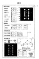
- the irradiation condition operation unit 19 includes an image display unit 20 that displays an observed image. Further, as an operation unit for irradiation conditions, an acceleration voltage setting unit 24, an irradiation current setting unit 25, a visual field size setting unit 26, a scanning speed setting unit 27, a normal scan / pulse scan switching unit 28, a pulse condition setting unit 29, a sample electric field A setting unit 30 is provided.
- the normal scan / pulse scan switching unit 28 can select a pulse scan when determining an irradiation condition for potential contrast, and can select a normal scan when determining other irradiation conditions.
- the pulse condition setting unit 29 can select a pulse scan condition that reflects the distance between irradiation points and the time between irradiation points.
- the distance threshold value display part 31 which displays the distance threshold value determined by S8 and the registration value of the distance threshold value registration part 22 is provided.
- the distance threshold value display unit 31 has a function of displaying the distance threshold value determined from the maximum luminance value in S8, a function of registering the distance threshold value determined in S8, and a function of selecting the distance threshold value from the registered value. is doing.
- the distance threshold value display unit 31 displays the distance between irradiation points stored in advance in a predetermined storage medium or the distance between irradiation points determined through the processing of Step 3 to Step 8, and the control system Beam scanning is performed at a plurality of irradiation point distances with longer distances between irradiation points, with the distance between irradiation points displayed on the display unit or the distance between irradiation points as a threshold value. Further, the control system evaluates the luminance difference between ROIs when the time between irradiation points is changed with the distance threshold or the distance between irradiation points equal to or greater than the distance threshold.
- the appropriate distance between irradiation points or the distance threshold varies depending on the material constituting the sample surface, so the sample type is displayed on the GUI screen, and the distance between irradiation points stored in association with the sample is set as the irradiation condition.
- the sample type is displayed on the GUI screen, and the distance between irradiation points stored in association with the sample is set as the irradiation condition.
- control range designating unit 32 for designating the control range of the distance between the irradiation points in S3 and the control range of the irradiation time interval in S9.
- ROI selection unit 33 that selects an ROI from an image is provided.
- the charging / discharging characteristic display unit 34 displays the relationship between the calculated luminance value and the distance between irradiation points in the range specified by the control range specifying unit 32 or the distance between irradiation points.
- the charge / discharge characteristic display unit 34 has a function of selecting and displaying whether to display the relationship between the luminance value and the distance between the irradiation points, or to display the relationship between the luminance value and the time between the irradiation points.
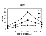
- the charge / discharge characteristic display unit 34 displays a graph with the luminance value as the vertical axis and the distance between the irradiation points as the horizontal axis, and displays the luminance value for each of the plurality of distances between the irradiation points of the plurality of ROIs. By performing such display, it is possible to grasp the distance between the irradiation points where the luminance value is maximum for each ROI, and while setting the distance between the irradiation points, the time between the irradiation points is changed, It is possible to specify an appropriate combination of the distance between the irradiation points and the time between the irradiation points.
- ROIA it is possible to grasp the distance between irradiation points suitable for any of ROIB and ROIC.
- a luminance value display unit 35 for displaying the maximum value of the luminance value difference in S14.
- an irradiation condition / brightness value registration button 36 for registering the determined irradiation condition and luminance value in the irradiation condition registration unit 21 and the luminance value registration unit 23 is provided.
- FIG. 4 shows a cross-sectional view of a part of the sample used in this example.
- the sample of FIG. 4 has a structure in which a columnar wiring 38 is buried between interlayer insulating films 37 of a silicon substrate 39 and an insulating film 40 is sandwiched between the wiring 38 and the silicon substrate 39.
- a columnar wiring 38 is buried between interlayer insulating films 37 of a silicon substrate 39 and an insulating film 40 is sandwiched between the wiring 38 and the silicon substrate 39.
- the thickness of the insulating film 40 and the polarity of the impurities contained in the silicon substrate 39 are different in each wiring 38, different electrical characteristics are shown in each wiring 38.
- FIG. 5 shows an image of the ROI selection unit 34 observed in this example.
- the three regions A, B, and C in FIG. 5, which are regions where the wiring 38 is exposed on the sample surface, are selected as ROIs, and in particular, the irradiation conditions are set by paying attention to the difference in luminance values between ROIA and ROIB.
- the control range designation unit 32 changes the distance between the irradiation points from 10 nm to 500 nm, and calculates the relationship between the ROI luminance value and the distance between the irradiation points. Indicates.
- the distance threshold was determined to be 100 nm from the distance between the irradiation points corresponding to the maximum luminance value of each ROI.
- the irradiation time interval is changed from 0.1 ⁇ s to 10 ⁇ s by the control range specifying unit 32 while the irradiation distance interval is kept at the distance threshold of 100 nm.
- the result of having calculated the relationship between the difference of the brightness value of ROIB and ROIB and the irradiation time interval is shown. From the maximum value of the difference between the brightness values of ROIA and ROIB, the time between irradiation points was determined to be 0.5 ⁇ s.
- the distance threshold value that is the distance between the irradiation points that maximizes the luminance value of the image is determined, and the luminance value between the plurality of regions is maintained while maintaining the distance between the irradiation points that is the distance threshold value.
- a distance threshold that is the distance between the irradiation points that maximizes the luminance value of the image is determined, and the distance between the irradiation points and the irradiation point is equal to or greater than the distance threshold so that the difference between the luminance values of the plurality of regions is maximized.
- Fig. 8 shows the flow for determining the irradiation conditions.
- the basic flow of this embodiment is the same as that shown in FIG.
- the difference between the flow shown in FIG. 8 and the flow shown in FIG. 2 is that S109 for designating the control range of the distance between the irradiation points and the time between the irradiation points within the range where the irradiation distance interval is equal to or greater than the distance threshold, and the irradiation point within the control range.
- step S110 the electron beam is scanned by changing the distance between the irradiation points and the time between the irradiation points to acquire an image.
- the normalized luminance value of the plurality of ROIs is selected from the combinations of the distances between the irradiation points and the scanning speed.
- the distance between the irradiation points and the time between the irradiation points are determined (S115).
- the distance between the irradiation points and the irradiation time interval are set to the values determined in S115 (S116).
- the GUI shown in FIG. 3 was used.
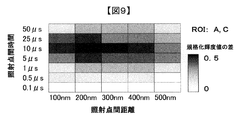
- the sample shown in FIG. 4 is used, and the three regions A, B, and C shown in FIG. 5 are selected as ROIs, and the irradiation conditions are focused on the difference in luminance values between ROIA and ROIC. It was determined. Since the relationship between the brightness value of the ROI and the distance between the irradiation points is the same as that in FIG. 6, the distance threshold is determined to be 100 nm.
- the distance between the irradiation points is changed in the range of 100 nm to 500 nm which is a distance threshold of 100 nm or more, and the time between the irradiation points is set to 10 ⁇ s by the control range designation unit 32.
- FIG. 9 shows the result of calculating the relationship between the difference between the normalized luminance values of ROIA and ROIC, the distance between the irradiation points, and the time between the irradiation points by changing the value from 100 ⁇ s to 100 ⁇ s.
- the distance between the irradiation points is taken on the horizontal axis, and the time between the irradiation points is taken on the vertical axis, and the color becomes darker as the difference in the normalized luminance value increases with respect to the combination of the distance between the irradiation points and the time between the irradiation points.
- the distance threshold that is the distance between the irradiation points that maximizes the luminance value of the image is determined, and the luminance values of the plurality of regions are maintained while maintaining the distance between the irradiation points that is the distance threshold.
- the feature amount for specifying the interval between the irradiation points and the time between the irradiation points, and the determination criterion for determining whether or not the predetermined state is used are: Various things can be used.
- a distance threshold that is a distance between irradiation points that minimizes the luminance value of the image (or is equal to or less than a predetermined threshold) is determined, and a plurality of distances are set in a state where the distance between the irradiation points corresponding to the distance threshold is set.
- a scanning electron microscope that observes the potential contrast derived from the charging characteristics of the sample with high accuracy by determining the time between the irradiation points so that the difference in the luminance values of the region of the above will be maximized will be described. In this example, the scanning electron microscope shown in FIG. 1 was used.
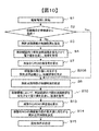
- FIG. 10 shows a flow for determining the irradiation conditions in order to observe the potential contrast derived from the charge characteristics of the sample with high accuracy.
- the basic flow of this embodiment is the same as that shown in FIG.
- a distance threshold is determined from the distance between irradiation points corresponding to the minimum value of the luminance value (S208).
- the GUI shown in FIG. 3 was used.
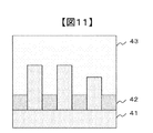
- FIG. 11 shows a cross-sectional view of the sample used in this example.
- the structure in which the inter-groove insulating film 42 is buried between the silicon 41 in which the grooves are formed is covered with a mask 43.
- the mask 43 exhibits different electrical characteristics between the regions.
- FIG. 12 shows an image of the ROI selection unit 33 observed in this example.
- the two regions D and E in FIG. 12 which are regions covered with the mask 43 immediately above the protrusions of the silicon 41, were selected as ROIs.
- the control range designation unit 32 changes the distance between the irradiation points from 10 nm to 250 nm, and calculates the relationship between the ROID luminance value and the irradiation distance interval. Show.
- the distance threshold value was determined to be 75 nm from the distance between irradiation points corresponding to the minimum value of the brightness value of ROID.
- the irradiation time interval is changed from 0.1 ⁇ s to 10 ⁇ s by the control range specifying unit 32 while the distance between the irradiation points is kept at the distance threshold value 75 nm.
- the result of having calculated the relationship between the difference of the brightness value of ROID and ROIE and the time between irradiation points is shown. From the maximum value of the difference between the brightness values of ROID and ROIE, the time between irradiation points was determined to be 1 ⁇ s.
- the distance threshold that is the distance between the irradiation points that minimizes the luminance value of the image is determined, and the luminance of the plurality of regions is maintained while maintaining the distance between the irradiation points corresponding to the distance threshold.
- a distance threshold that is a distance between irradiation points that minimizes the luminance value of the image is determined, and the distance between the irradiation points and the irradiation point is equal to or larger than the distance threshold so that the difference between the luminance values of a plurality of regions is maximized.
- FIG. 15 shows a flow for determining the irradiation conditions in order to observe the potential contrast derived from the discharge characteristics of the sample with high accuracy.
- the basic flow of this embodiment is the same as that shown in FIG.
- a distance threshold is determined from the distance between irradiation points corresponding to the minimum value of the luminance value (S208).
- the GUI shown in FIG. 3 was used.
- FIG. 16 shows a cross-sectional view of a part of the sample used in this example.
- a contact plug 45 is embedded between the interlayer insulating films 44, a silicon substrate 46 is embedded below the contact plug 45, and an ion implantation layer 47 is formed at the junction between the contact plug 45 and the silicon substrate 46.
- the structure is made.
- FIG. 17 shows an image of the ROI selection unit 33 observed in this example.
- two regions F and G in FIG. 17 where the contact plug 45 was exposed on the sample surface were selected as ROIs.
- the control range designation unit 32 changes the distance between irradiation points between 50 nm and 500 nm, and calculates the relationship between the brightness value of ROIF and the distance between irradiation points. Indicates.
- the distance threshold was determined to be 200 nm from the distance between the irradiation points corresponding to the minimum value of the brightness value of ROIF.
- the control range specifying unit 32 changes the distance between the irradiation points in the range of 200 nm to 500 nm which is a distance threshold of 200 nm or more.
- the time is changed between 0.1 ⁇ s and 5 ⁇ s, and the result of calculating the relationship between the difference between the normalized luminance values of ROIF and ROIG, the distance between irradiation points, and the time between irradiation points is shown.
- the horizontal axis indicates the distance between the irradiation points
- the vertical axis indicates the time between the irradiation points.
- the distance between irradiation points was determined to be 300 nm and the time between irradiation points was determined to be 1 ⁇ s from the combination of the distance between irradiation points and the time between irradiation points that maximized the difference in the normalized luminance values of F and G ROIs.
- a distance threshold that is the distance between the irradiation points that minimizes the luminance value of the image is determined, and the distance between the irradiation points is equal to or larger than the distance threshold so that the difference in the luminance values of the plurality of regions is maximized.
- FIG. 20 shows a flow for determining the irradiation conditions in order to observe the potential contrast derived from the discharge characteristics of the sample with high accuracy.
- the irradiation condition includes a scanning speed and a distance between irradiation points, which are control parameters for the distance between irradiation points and the time between irradiation points, and includes one or more irradiation charges, acceleration voltage, and sample electric field. Move to the observation location so that the ROI falls within the field of view (S1).
- the process proceeds to S303. If the ROI is registered with a distance threshold, the distance threshold is selected from the distance threshold registration unit 22, and the process proceeds to S304. Next, a distance threshold is determined using the flow shown in FIG. 2, FIG. 8, FIG. 10, or FIG. 15 (S303).
- control range of the irradiation charge amount, the acceleration voltage, and the sample electric field is designated (S304).
- the distance threshold, the irradiation charge amount, the acceleration voltage, and the sample electric field are changed within the control range, and the electron beam is scanned to acquire an image (S305).
- the brightness value of the ROI is calculated from the image (S308).
- the luminance value is determined from the maximum value of the luminance value, and when the distance threshold is determined using the flow of FIG. 10 or FIG.
- the irradiation charge amount, the acceleration voltage, and the sample electric field are determined from the minimum value of (S309).
- the time between irradiation points, or the distance between irradiation points and the time between irradiation points are determined (S310).
- irradiation conditions are set for setting the irradiation charge amount, acceleration voltage, sample electric field, distance between irradiation points, and time between irradiation points to the values determined in S115 (S311).
- FIG. 21 shows the GUI used in this example.
- the basic configuration of the GUI is the same as in FIG.
- the GUI of the present embodiment includes a control range specifying unit 48 that specifies the control range of the irradiation charge amount, the acceleration voltage, and the sample electric field in S304 in addition to the control range of the distance between irradiation points and the time between irradiation points. .
- FIG. 22 shows a cross-sectional view of a part of the sample used in this example.
- the sample of FIG. 22 has a structure in which a wiring 50 is buried between interlayer insulating films 49, and an electrode 51, an insulating film 52, and an electrode 51 are sequentially stacked below the wiring 50.
- the wiring 50 exhibits different electrical characteristics from the other wirings 50.
- FIG. 23 shows an image of the ROI selection unit 33 observed in this example. In this embodiment, two regions H and I in FIG. 23, which are regions where the wiring 53 is exposed on the sample surface, are selected as ROIs.
- FIG. 23 shows an image of the ROI selection unit 33 observed in this example. In this embodiment, two regions H and I in FIG. 23, which are regions where the wiring 53 is exposed on the sample surface, are selected as ROIs.
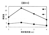
- the 24 shows the result of calculating the relationship between the ROI luminance value and the irradiation charge amount by changing the irradiation charge amount between 1 nC and 4 nC in the control range specifying unit 48 in order to determine the irradiation charge amount in this example. Show.
- the irradiation charge amount was determined to be 2 nC from the irradiation charge amount corresponding to the maximum luminance value of each ROI. By determining the irradiation charge amount in this way, the electrical characteristics of the ROI can be more strongly reflected in the potential contrast.
- the potential contrast of the sample could be observed with high accuracy by determining the irradiation charge amount, acceleration voltage, and sample electric field when irradiating the charged particle beam while keeping the distance between the irradiation points at the distance threshold.
- the observation region specified using the registered irradiation condition and the luminance value is measured, and the coordinates of the same luminance value as the registered luminance value are automatically determined, whereby the ROI coordinates in the observation region are automatically determined.
- the scanning electron microscope to be determined will be described. In this example, the scanning electron microscope shown in FIG. 1 was used.
- FIG. 25 shows a flow for automatically determining the coordinates of the ROI in the observation area in the present embodiment.
- a sample type is designated (S401). By specifying the type of the sample, the irradiation condition registered in the irradiation condition registration unit 21 is set.
- An observation area is designated (S402). The observation start button 56 is pressed (S403). The observation start button 56 will be described later with reference to FIG. Observation is automatically performed under the registered irradiation conditions, and the coordinates of the ROI are automatically determined from the luminance value of the image (S404).
- FIG. 26 shows the GUI used in this example.
- the image / coordinate display unit 53 has a sample designating unit 54 for designating the type of sample. Moreover, it has the observation coordinate setting part 55 which sets the coordinate to observe. Moreover, it has the observation start button 56 which starts automatic observation.
- an ROI coordinate display unit 57 that displays the coordinates of the ROI determined in S404 is provided.
- the sample shown in FIG. 4 was used, and the three regions A, B, and C shown in FIG. 5 were selected as ROIs. Part of the automatically determined ROI coordinates is shown in the ROI coordinate display section 57 of FIG.
- the designated observation region is measured using the registered irradiation condition and the luminance value, and the coordinates of the same luminance value as the registered luminance value are automatically determined.
- the coordinates of the ROI could be determined automatically.
- the electron beam is used for observing the sample.
- the electron beam is used for observing the sample.
- the electron beam is used for observing the sample.
- other charged particle beams can be observed similarly.
- SYMBOLS 1 Electron source, 2 ... Deflector, 3 ... Objective lens, 4 ... Detector, 5 ... Irradiation / non-irradiation switching part, 6 ... Diaphragm, 7 ... XYZ stage, 8 ... Sample holder, 9 ... Sample, 10 ... Electron Source control unit, 11 ... deflection signal control unit, 12 ... objective lens coil control unit, 13 ... detector control unit, 14 ... XYZ stage control unit, 15 ... sample electric field control unit, 16 ... irradiation / non-irradiation control unit, 17 DESCRIPTION OF SYMBOLS ... Detection signal processing part, 18 ... Image formation part, 19 ...
- Irradiation condition operation part 20 ... Image display part, 21 ... Irradiation condition registration part, 22 ... Distance threshold value registration part, 23 ... Luminance value registration part, 24 ... Acceleration voltage Setting unit 25 ... Irradiation current setting unit 26 ... Field size setting unit 27 ... Scanning speed setting unit 28 ... Normal scan / pulse scan switching unit 29 ... Pulse condition setting unit 30 ... Sample electric field setting unit 31 ... Distance threshold value display part, 32 ... control range Fixed part 33 ... ROI selection part 34 ... Charge / discharge characteristic display part 35 ... Brightness value display part 36 ... Irradiation condition / brightness value registration button 37 ... Interlayer insulating film 38 ... Wiring 39 ... Silicon substrate 40 ... Insulating film, 41 ...
Landscapes
- Chemical & Material Sciences (AREA)
- Analytical Chemistry (AREA)
- Engineering & Computer Science (AREA)
- Computer Vision & Pattern Recognition (AREA)
- Analysing Materials By The Use Of Radiation (AREA)
- Testing Or Measuring Of Semiconductors Or The Like (AREA)
Abstract
Description
照射点間距離を距離閾値に保ちながら、荷電粒子線を照射する際の照射電荷量及び加速電圧及び試料電界を決定することで、試料の電位コントラストを高精度で観察することができた。
Claims (18)
- ビームをパルス状に照射しつつ、ビーム走査を行うときのビーム照射条件決定方法であって、
前記パルス状ビームの照射点間距離を変化させ、
照射点間距離の異なる複数の画像を取得し、
当該照射点間距離の異なる複数の画像の特定領域の特徴量を評価し、
当該特徴量が所定の状態となるようなビームの照射点間距離を特定し、
当該特定された照射点間距離を設定、或いは当該特定された照射点間距離に基づいて定められる複数の照射点間距離を設定し、
当該特定された照射点間距離、或いは複数の照射点間距離が設定された状態にて、前記パルス状ビームの照射点間時間を変化させたときに得られる複数の画像に含まれる複数の特定領域を評価し、
当該複数の特定領域の特徴量が所定の状態となる照射点間時間を特定することを特徴とする荷電粒子線装置の照射条件決定方法。 - 請求項1において、
前記照射点間間隔の異なる複数の画像の特定領域の特徴量を評価するときに、前記特定領域の輝度値を評価することを特徴とする荷電粒子線装置の照射条件決定方法。 - 請求項2において、
前記特定領域の輝度値が最小、最大、所定の閾値以上、或いは所定の閾値以下のビームの照射点間間隔を特定することを特徴とする荷電粒子線装置の照射条件決定方法。 - 請求項1において、
前記照射点間時間を特定するときに、前記複数の特定領域間の輝度差が最大、或いは所定値の閾値以上となる照射点間時間を特定することを特徴とする荷電粒子線装置の照射条件決定方法。 - 請求項1において、
前記複数の照射点間距離が設定された状態にて、複数の照射点間時間を設定し、前記複数の特定領域の特徴量が所定の状態となる照射点間距離と照射点間時間の組み合わせを特定することを特徴とする荷電粒子線装置の照射条件決定方法。 - 請求項5において、
前記複数の特定領域間の輝度差が最大、或いは所定の閾値以上となる照射点間距離と照射点間時間の組み合わせを特定することを特徴とする荷電粒子線装置の照射条件決定方法。 - ビームを走査する走査偏向器を有し、当該走査偏向器によって走査されるビームをパルス状に試料に照射するビームカラムと、
前記試料に対するビームの照射によって得られる粒子を検出する検出器と、
前記ビームカラムを制御する制御システムを備え、
当該制御システムは、前記検出器の出力を処理することによって、1以上の画像の特徴量を取得するように構成され、前記制御システムは、前記検出器の出力に基づいて得られる画像の1以上の特定領域の特徴量が所定の状態となるような前記パルス状のビームの照射点間距離を特定し、当該特定された照射点間距離が設定された状態、或いは当該特定された照射点間距離に基づいて定められる複数の照射点間距離が設定された状態にて、前記パルス状ビームの照射点間時間を変化させ、前記検出器の出力に基づいて得られる画像の複数の特定領域の特徴量が所定の状態となる照射点間時間でビーム照射するように指示するように構成されていることを特徴とする荷電粒子線装置。 - 請求項7において、
前記ビームカラムは、前記ビームを軸外に偏向するパルスビーム生成用偏向器を備え、前記制御システムは、設定された照射点間距離及び照射点間時間に応じたパルスビームとなるように、前記走査偏向器とパルスビーム用偏向器を制御することを特徴とする荷電粒子線装置。 - 請求項8において、
前記制御システムは、前記照射点間距離の異なる複数の画像の特定領域の特徴量の評価に基づいて特定された照射点間距離で前記ビームを照射するように、前記走査偏向器とパルスビーム生成用偏向器を制御することを特徴とする荷電粒子線装置。 - 請求項9において、
前記制御システムは、前記特定領域の輝度値が最小、最大、所定の閾値以上、或いは所定の閾値以下のビームの照射点間間隔となるように、前記走査偏向器とパルスビーム生成用偏向器を制御することを特徴とする荷電粒子線装置。 - 請求項7において、
前記制御システムは、前記複数の特定領域間の輝度差が最大、或いは所定値の閾値以上となる照射点間時間でビームを走査するように、前記パルスビーム生成用偏向器を制御することを特徴とする荷電粒子線装置。 - 請求項7において、
前記制御システムは、前記複数の照射点間距離が設定された状態にて、複数の照射点間時間を設定し、前記複数の特定領域の特徴量が所定の状態となる照射点間距離と照射点間時間の組み合わせで前記ビームを走査するように、前記走査偏向器と前記パルスビーム生成用偏向器を制御することを特徴とする荷電粒子線装置。 - 請求項12において、
前記制御システムは、前記複数の特定領域間の輝度差が最大、或いは所定の閾値以上となる照射点間距離と照射点間時間の組み合わせでビームを走査するように、前記走査偏向器と前記パルスビーム生成用偏向器を制御することを特徴とする荷電粒子線装置。 - 請求項7において、
前記検出器の出力に基づいて前記特定領域の輝度を評価する1以上のプロセッサを備え、当該プロセッサは、前記特定領域の輝度値と前記照射点間距離との関係に基づいて、前記輝度値が最大となる照射点間距離を決定することを特徴とする荷電粒子線装置。 - 荷電粒子線装置を制御するパラメータを決定するためにコンピューターシステム上で実行されるプログラム命令を格納するコンピューター読み取り可能な媒体であって、
前記荷電粒子線装置のパルス状ビームの照射点間距離を変化させたときの照射点間距離の異なる複数の画像を取得し、
当該照射点間距離の異なる複数の画像の特定領域の特徴量を評価し、
当該特徴量が所定の状態となるようなビームの照射点間距離を特定し、
当該特定された照射点間距離、或いは当該特定された照射点間距離に基づいて定められる複数の照射点間距離が設定された状態にて、前記パルス状ビームの照射点間時間を変化させたときに得られる複数の画像に含まれる複数の特定領域を評価し、
当該複数の特定領域の特徴量が所定の状態となる照射点間時間を特定することを特徴とするコンピューター読み取り可能な媒体。 - 試料に対して荷電粒子ビームを照射する荷電粒子線装置であって、
ビームを走査する走査偏向器を有し、当該走査偏向器によって走査されるビームをパルス状に試料に照射するビームカラムと、前記試料に対するビームの照射によって得られる粒子を検出する検出器と、前記ビームカラムを制御する制御システムを有する荷電粒子ビーム照射システムと、
前記制御システムの制御条件を表示する表示装置を備え、
当該表示装置には少なくとも前記パルス状ビームの照射点間距離に関する情報が表示され、前記制御システムは、前記表示された照射点間距離、或いは前記表示された照射点間距離を閾値とした複数の照射点間距離で、ビームを走査するように設定した状態で、前記パルス状ビームの照射点間時間を変化させることによって、1の照射点間距離に対して複数の画像を取得し、当該複数の画像に含まれる特定領域の特徴量を評価することによって、当該特徴量が所定の状態となる照射点間時間を特定することを特徴とする荷電粒子線装置。 - 試料に対して荷電粒子ビームを照射する荷電粒子線装置であって、
ビームを走査する走査偏向器を有し、当該走査偏向器によって走査されるビームをパルス状に試料に照射するビームカラムと、前記試料に対するビームの照射によって得られる粒子を検出する検出器と、前記ビームカラムを制御する制御システムを有する荷電粒子ビーム照射システムと、
前記制御システムの制御条件を表示する表示装置を備え、
前記制御システムは、前記パルス状のビームの照射点間距離、或いは照射点間時間を複数の状態に設定した状態で、前記ビームを照射することによって、複数の照射点間距離ごと、或いは複数の照射点間時間の画像を取得し、当該画像に含まれる複数の特定領域の特徴量を評価し、前記複数の照射点間距離ごと、或いは前記複数の照射点間時間の複数の特徴量に関する情報を、前記表示装置に表示させることを特徴とする荷電粒子線装置。 - 請求項17において、
前記制御システムは、前記照射点間距離ごとの複数の特徴量の最大値を、前記表示装置に表示させることを特徴とする荷電粒子線装置。
Priority Applications (4)
| Application Number | Priority Date | Filing Date | Title |
|---|---|---|---|
| JP2020515359A JP6937433B2 (ja) | 2018-04-25 | 2018-04-25 | 荷電粒子線装置の照射条件決定方法、及び荷電粒子線装置 |
| KR1020207026432A KR102478945B1 (ko) | 2018-04-25 | 2018-04-25 | 하전 입자선 장치의 조사 조건 결정 방법, 및 하전 입자선 장치 |
| US17/040,141 US11232929B2 (en) | 2018-04-25 | 2018-04-25 | Method for determining irradiation conditions for charged particle beam device and charged particle beam device |
| PCT/JP2018/016741 WO2019207668A1 (ja) | 2018-04-25 | 2018-04-25 | 荷電粒子線装置の照射条件決定方法、及び荷電粒線装置 |
Applications Claiming Priority (1)
| Application Number | Priority Date | Filing Date | Title |
|---|---|---|---|
| PCT/JP2018/016741 WO2019207668A1 (ja) | 2018-04-25 | 2018-04-25 | 荷電粒子線装置の照射条件決定方法、及び荷電粒線装置 |
Publications (1)
| Publication Number | Publication Date |
|---|---|
| WO2019207668A1 true WO2019207668A1 (ja) | 2019-10-31 |
Family
ID=68294918
Family Applications (1)
| Application Number | Title | Priority Date | Filing Date |
|---|---|---|---|
| PCT/JP2018/016741 Ceased WO2019207668A1 (ja) | 2018-04-25 | 2018-04-25 | 荷電粒子線装置の照射条件決定方法、及び荷電粒線装置 |
Country Status (4)
| Country | Link |
|---|---|
| US (1) | US11232929B2 (ja) |
| JP (1) | JP6937433B2 (ja) |
| KR (1) | KR102478945B1 (ja) |
| WO (1) | WO2019207668A1 (ja) |
Cited By (1)
| Publication number | Priority date | Publication date | Assignee | Title |
|---|---|---|---|---|
| WO2023026489A1 (ja) * | 2021-08-27 | 2023-03-02 | 株式会社日立ハイテク | コンピュータシステムおよび解析方法 |
Families Citing this family (2)
| Publication number | Priority date | Publication date | Assignee | Title |
|---|---|---|---|---|
| CN115184248B (zh) * | 2022-06-23 | 2025-11-04 | 岭东核电有限公司 | 粒子辐照与高温液体腐蚀耦合效应的测试装置及测试方法 |
| CN116068003B (zh) * | 2022-12-19 | 2025-09-26 | 中国原子能科学研究院 | 辐照条件下的状态确定方法、装置、设备及介质 |
Citations (6)
| Publication number | Priority date | Publication date | Assignee | Title |
|---|---|---|---|---|
| JP2000208085A (ja) * | 1999-01-08 | 2000-07-28 | Schlumberger Technol Inc | 低電圧粒子ビ―ムを用いた半導体検査用の電圧コントラスト方法及び装置 |
| JP2002009121A (ja) * | 2000-06-19 | 2002-01-11 | Hitachi Ltd | 半導体装置の検査方法及び検査装置、及びそれを用いた半導体装置の製造方法 |
| JP2004266182A (ja) * | 2003-03-04 | 2004-09-24 | Hitachi High-Technologies Corp | 電子線描画装置 |
| WO2012165293A1 (ja) * | 2011-06-03 | 2012-12-06 | 株式会社日立ハイテクノロジーズ | 電子顕微鏡及び電子線を用いた撮像方法 |
| WO2013035220A1 (ja) * | 2011-09-05 | 2013-03-14 | 株式会社 日立ハイテクノロジーズ | 荷電粒子線装置 |
| WO2015045498A1 (ja) * | 2013-09-26 | 2015-04-02 | 株式会社 日立ハイテクノロジーズ | 荷電粒子線装置 |
Family Cites Families (4)
| Publication number | Priority date | Publication date | Assignee | Title |
|---|---|---|---|---|
| JPS54142214A (en) | 1978-04-28 | 1979-11-06 | Tdk Electronics Co Ltd | High permittivity ceramic composition |
| JPS56139580A (en) | 1980-03-31 | 1981-10-31 | Kuraray Co Ltd | Modified polyvinyl alcohol soil conditioner |
| JP4914180B2 (ja) * | 2006-11-08 | 2012-04-11 | 株式会社日立ハイテクノロジーズ | 時定数測定機能を搭載した走査型電子顕微鏡 |
| JP6379018B2 (ja) * | 2014-11-20 | 2018-08-22 | 株式会社日立ハイテクノロジーズ | 荷電粒子線装置および検査方法 |
-
2018
- 2018-04-25 WO PCT/JP2018/016741 patent/WO2019207668A1/ja not_active Ceased
- 2018-04-25 US US17/040,141 patent/US11232929B2/en active Active
- 2018-04-25 KR KR1020207026432A patent/KR102478945B1/ko active Active
- 2018-04-25 JP JP2020515359A patent/JP6937433B2/ja active Active
Patent Citations (6)
| Publication number | Priority date | Publication date | Assignee | Title |
|---|---|---|---|---|
| JP2000208085A (ja) * | 1999-01-08 | 2000-07-28 | Schlumberger Technol Inc | 低電圧粒子ビ―ムを用いた半導体検査用の電圧コントラスト方法及び装置 |
| JP2002009121A (ja) * | 2000-06-19 | 2002-01-11 | Hitachi Ltd | 半導体装置の検査方法及び検査装置、及びそれを用いた半導体装置の製造方法 |
| JP2004266182A (ja) * | 2003-03-04 | 2004-09-24 | Hitachi High-Technologies Corp | 電子線描画装置 |
| WO2012165293A1 (ja) * | 2011-06-03 | 2012-12-06 | 株式会社日立ハイテクノロジーズ | 電子顕微鏡及び電子線を用いた撮像方法 |
| WO2013035220A1 (ja) * | 2011-09-05 | 2013-03-14 | 株式会社 日立ハイテクノロジーズ | 荷電粒子線装置 |
| WO2015045498A1 (ja) * | 2013-09-26 | 2015-04-02 | 株式会社 日立ハイテクノロジーズ | 荷電粒子線装置 |
Cited By (4)
| Publication number | Priority date | Publication date | Assignee | Title |
|---|---|---|---|---|
| WO2023026489A1 (ja) * | 2021-08-27 | 2023-03-02 | 株式会社日立ハイテク | コンピュータシステムおよび解析方法 |
| JPWO2023026489A1 (ja) * | 2021-08-27 | 2023-03-02 | ||
| TWI823510B (zh) * | 2021-08-27 | 2023-11-21 | 日商日立全球先端科技股份有限公司 | 電腦系統及解析方法 |
| JP7700248B2 (ja) | 2021-08-27 | 2025-06-30 | 株式会社日立ハイテク | コンピュータシステムおよび解析方法 |
Also Published As
| Publication number | Publication date |
|---|---|
| KR102478945B1 (ko) | 2022-12-19 |
| JP6937433B2 (ja) | 2021-09-22 |
| US11232929B2 (en) | 2022-01-25 |
| US20210027981A1 (en) | 2021-01-28 |
| KR20200120719A (ko) | 2020-10-21 |
| JPWO2019207668A1 (ja) | 2021-05-13 |
Similar Documents
| Publication | Publication Date | Title |
|---|---|---|
| JP4093662B2 (ja) | 走査形電子顕微鏡 | |
| EP0661727B1 (en) | Scanning electron microscope | |
| US9236220B2 (en) | Electronic microscope, setting method of observation condition of electronic microscope, and observation method using electronic microscope | |
| US8969801B2 (en) | Scanning electron microscope | |
| US9941095B2 (en) | Charged particle beam apparatus | |
| US20080174772A1 (en) | Circuit-pattern inspection apparatus | |
| JP2006107919A (ja) | 荷電粒子線装置および寸法測定方法 | |
| JPH05151927A (ja) | 走査型電子顕微鏡およびその観察方法 | |
| JP6937433B2 (ja) | 荷電粒子線装置の照射条件決定方法、及び荷電粒子線装置 | |
| JP2019027938A (ja) | マテリアルインフォマティクスを実現する画像処理装置 | |
| JP5117080B2 (ja) | 試料観察条件設定方法及び装置、並びに試料観察方法及び装置 | |
| JP5388039B2 (ja) | 画像を生成するための方法および装置 | |
| JP7174773B2 (ja) | 荷電粒子線装置の調整方法及び荷電粒子線装置システム | |
| JP2005005055A (ja) | 試料の高さ情報取得方法 | |
| JP2006172919A (ja) | 三次元形状解析機能を有する走査型電子顕微鏡 | |
| US10629408B2 (en) | Charged particle beam device | |
| JP4658783B2 (ja) | 試料像形成方法 | |
| JP2022071251A (ja) | 荷電粒子線装置 | |
| JPH10208683A (ja) | 走査形電子顕微鏡 | |
| JP5500868B2 (ja) | 走査電子顕微鏡、および走査電子顕微鏡における像表示方法 | |
| JP2009187851A (ja) | 荷電粒子ビーム装置、及び試料の表面の帯電状態を知る方法 |
Legal Events
| Date | Code | Title | Description |
|---|---|---|---|
| 121 | Ep: the epo has been informed by wipo that ep was designated in this application |
Ref document number: 18915858 Country of ref document: EP Kind code of ref document: A1 |
|
| ENP | Entry into the national phase |
Ref document number: 20207026432 Country of ref document: KR Kind code of ref document: A |
|
| ENP | Entry into the national phase |
Ref document number: 2020515359 Country of ref document: JP Kind code of ref document: A |
|
| NENP | Non-entry into the national phase |
Ref country code: DE |
|
| 122 | Ep: pct application non-entry in european phase |
Ref document number: 18915858 Country of ref document: EP Kind code of ref document: A1 |