WO2019159702A1 - フルカラーled表示パネル及びその製造方法 - Google Patents
フルカラーled表示パネル及びその製造方法 Download PDFInfo
- Publication number
- WO2019159702A1 WO2019159702A1 PCT/JP2019/003452 JP2019003452W WO2019159702A1 WO 2019159702 A1 WO2019159702 A1 WO 2019159702A1 JP 2019003452 W JP2019003452 W JP 2019003452W WO 2019159702 A1 WO2019159702 A1 WO 2019159702A1
- Authority
- WO
- WIPO (PCT)
- Prior art keywords
- fluorescent
- light
- light emitting
- display panel
- emitting layer
- Prior art date
- Legal status (The legal status is an assumption and is not a legal conclusion. Google has not performed a legal analysis and makes no representation as to the accuracy of the status listed.)
- Ceased
Links
Images







Classifications
-
- H—ELECTRICITY
- H10—SEMICONDUCTOR DEVICES; ELECTRIC SOLID-STATE DEVICES NOT OTHERWISE PROVIDED FOR
- H10H—INORGANIC LIGHT-EMITTING SEMICONDUCTOR DEVICES HAVING POTENTIAL BARRIERS
- H10H29/00—Integrated devices, or assemblies of multiple devices, comprising at least one light-emitting semiconductor element covered by group H10H20/00
- H10H29/10—Integrated devices comprising at least one light-emitting semiconductor component covered by group H10H20/00
- H10H29/14—Integrated devices comprising at least one light-emitting semiconductor component covered by group H10H20/00 comprising multiple light-emitting semiconductor components
- H10H29/142—Two-dimensional arrangements, e.g. asymmetric LED layout
-
- H—ELECTRICITY
- H10—SEMICONDUCTOR DEVICES; ELECTRIC SOLID-STATE DEVICES NOT OTHERWISE PROVIDED FOR
- H10W—GENERIC PACKAGES, INTERCONNECTIONS, CONNECTORS OR OTHER CONSTRUCTIONAL DETAILS OF DEVICES COVERED BY CLASS H10
- H10W90/00—Package configurations
-
- G—PHYSICS
- G02—OPTICS
- G02B—OPTICAL ELEMENTS, SYSTEMS OR APPARATUS
- G02B5/00—Optical elements other than lenses
- G02B5/20—Filters
-
- G—PHYSICS
- G09—EDUCATION; CRYPTOGRAPHY; DISPLAY; ADVERTISING; SEALS
- G09F—DISPLAYING; ADVERTISING; SIGNS; LABELS OR NAME-PLATES; SEALS
- G09F9/00—Indicating arrangements for variable information in which the information is built-up on a support by selection or combination of individual elements
-
- G—PHYSICS
- G09—EDUCATION; CRYPTOGRAPHY; DISPLAY; ADVERTISING; SEALS
- G09F—DISPLAYING; ADVERTISING; SIGNS; LABELS OR NAME-PLATES; SEALS
- G09F9/00—Indicating arrangements for variable information in which the information is built-up on a support by selection or combination of individual elements
- G09F9/30—Indicating arrangements for variable information in which the information is built-up on a support by selection or combination of individual elements in which the desired character or characters are formed by combining individual elements
- G09F9/33—Indicating arrangements for variable information in which the information is built-up on a support by selection or combination of individual elements in which the desired character or characters are formed by combining individual elements being semiconductor devices, e.g. diodes
- G09F9/335—Indicating arrangements for variable information in which the information is built-up on a support by selection or combination of individual elements in which the desired character or characters are formed by combining individual elements being semiconductor devices, e.g. diodes being organic light emitting diodes [OLED]
-
- H—ELECTRICITY
- H10—SEMICONDUCTOR DEVICES; ELECTRIC SOLID-STATE DEVICES NOT OTHERWISE PROVIDED FOR
- H10H—INORGANIC LIGHT-EMITTING SEMICONDUCTOR DEVICES HAVING POTENTIAL BARRIERS
- H10H20/00—Individual inorganic light-emitting semiconductor devices having potential barriers, e.g. light-emitting diodes [LED]
- H10H20/01—Manufacture or treatment
-
- H—ELECTRICITY
- H10—SEMICONDUCTOR DEVICES; ELECTRIC SOLID-STATE DEVICES NOT OTHERWISE PROVIDED FOR
- H10H—INORGANIC LIGHT-EMITTING SEMICONDUCTOR DEVICES HAVING POTENTIAL BARRIERS
- H10H20/00—Individual inorganic light-emitting semiconductor devices having potential barriers, e.g. light-emitting diodes [LED]
- H10H20/01—Manufacture or treatment
- H10H20/011—Manufacture or treatment of bodies, e.g. forming semiconductor layers
- H10H20/018—Bonding of wafers
-
- H—ELECTRICITY
- H10—SEMICONDUCTOR DEVICES; ELECTRIC SOLID-STATE DEVICES NOT OTHERWISE PROVIDED FOR
- H10H—INORGANIC LIGHT-EMITTING SEMICONDUCTOR DEVICES HAVING POTENTIAL BARRIERS
- H10H20/00—Individual inorganic light-emitting semiconductor devices having potential barriers, e.g. light-emitting diodes [LED]
- H10H20/01—Manufacture or treatment
- H10H20/034—Manufacture or treatment of coatings
-
- H—ELECTRICITY
- H10—SEMICONDUCTOR DEVICES; ELECTRIC SOLID-STATE DEVICES NOT OTHERWISE PROVIDED FOR
- H10H—INORGANIC LIGHT-EMITTING SEMICONDUCTOR DEVICES HAVING POTENTIAL BARRIERS
- H10H20/00—Individual inorganic light-emitting semiconductor devices having potential barriers, e.g. light-emitting diodes [LED]
- H10H20/01—Manufacture or treatment
- H10H20/036—Manufacture or treatment of packages
- H10H20/0361—Manufacture or treatment of packages of wavelength conversion means
-
- H—ELECTRICITY
- H10—SEMICONDUCTOR DEVICES; ELECTRIC SOLID-STATE DEVICES NOT OTHERWISE PROVIDED FOR
- H10H—INORGANIC LIGHT-EMITTING SEMICONDUCTOR DEVICES HAVING POTENTIAL BARRIERS
- H10H20/00—Individual inorganic light-emitting semiconductor devices having potential barriers, e.g. light-emitting diodes [LED]
- H10H20/01—Manufacture or treatment
- H10H20/036—Manufacture or treatment of packages
- H10H20/0363—Manufacture or treatment of packages of optical field-shaping means
-
- H—ELECTRICITY
- H10—SEMICONDUCTOR DEVICES; ELECTRIC SOLID-STATE DEVICES NOT OTHERWISE PROVIDED FOR
- H10H—INORGANIC LIGHT-EMITTING SEMICONDUCTOR DEVICES HAVING POTENTIAL BARRIERS
- H10H20/00—Individual inorganic light-emitting semiconductor devices having potential barriers, e.g. light-emitting diodes [LED]
- H10H20/80—Constructional details
- H10H20/85—Packages
- H10H20/851—Wavelength conversion means
- H10H20/8511—Wavelength conversion means characterised by their material, e.g. binder
-
- H—ELECTRICITY
- H10—SEMICONDUCTOR DEVICES; ELECTRIC SOLID-STATE DEVICES NOT OTHERWISE PROVIDED FOR
- H10H—INORGANIC LIGHT-EMITTING SEMICONDUCTOR DEVICES HAVING POTENTIAL BARRIERS
- H10H20/00—Individual inorganic light-emitting semiconductor devices having potential barriers, e.g. light-emitting diodes [LED]
- H10H20/80—Constructional details
- H10H20/85—Packages
- H10H20/851—Wavelength conversion means
- H10H20/8511—Wavelength conversion means characterised by their material, e.g. binder
- H10H20/8512—Wavelength conversion materials
- H10H20/8513—Wavelength conversion materials having two or more wavelength conversion materials
-
- H—ELECTRICITY
- H10—SEMICONDUCTOR DEVICES; ELECTRIC SOLID-STATE DEVICES NOT OTHERWISE PROVIDED FOR
- H10H—INORGANIC LIGHT-EMITTING SEMICONDUCTOR DEVICES HAVING POTENTIAL BARRIERS
- H10H20/00—Individual inorganic light-emitting semiconductor devices having potential barriers, e.g. light-emitting diodes [LED]
- H10H20/80—Constructional details
- H10H20/85—Packages
- H10H20/851—Wavelength conversion means
- H10H20/8515—Wavelength conversion means not being in contact with the bodies
-
- H—ELECTRICITY
- H10—SEMICONDUCTOR DEVICES; ELECTRIC SOLID-STATE DEVICES NOT OTHERWISE PROVIDED FOR
- H10H—INORGANIC LIGHT-EMITTING SEMICONDUCTOR DEVICES HAVING POTENTIAL BARRIERS
- H10H20/00—Individual inorganic light-emitting semiconductor devices having potential barriers, e.g. light-emitting diodes [LED]
- H10H20/80—Constructional details
- H10H20/85—Packages
- H10H20/855—Optical field-shaping means, e.g. lenses
- H10H20/856—Reflecting means
-
- H—ELECTRICITY
- H10—SEMICONDUCTOR DEVICES; ELECTRIC SOLID-STATE DEVICES NOT OTHERWISE PROVIDED FOR
- H10H—INORGANIC LIGHT-EMITTING SEMICONDUCTOR DEVICES HAVING POTENTIAL BARRIERS
- H10H20/00—Individual inorganic light-emitting semiconductor devices having potential barriers, e.g. light-emitting diodes [LED]
- H10H20/80—Constructional details
- H10H20/85—Packages
- H10H20/857—Interconnections, e.g. lead-frames, bond wires or solder balls
Definitions
- the present invention relates to a full-color LED display panel provided with a fluorescent light-emitting layer, and particularly to a full-color LED display panel that can shorten the manufacturing process and suppress an increase in the thickness of the fluorescent light-emitting layer, and a manufacturing method thereof.
- a conventional full-color LED display panel has a red phosphor layer and a red color filter on an organic EL element substrate provided with a plurality of organic EL elements that emit blue or blue-green light, corresponding to the organic EL element corresponding to red.
- the layer thickness of the color conversion substrate is increased and the rigidity is increased. For example, the flexibility of a flexible display panel may be lost.
- an object of the present invention is to provide a full-color LED display panel that can cope with such problems, shorten the manufacturing process, and suppress an increase in the thickness of the fluorescent light-emitting layer, and a manufacturing method thereof.
- a full-color LED display panel includes an LED array substrate in which a plurality of LEDs that emit light in the ultraviolet or blue wavelength band are arranged in a matrix on a wiring substrate, and a plurality of three-color LEDs.
- a fluorescent dye and an adjustment dye that selectively transmits light in a predetermined wavelength band are uniformly dispersed on the LED, and are excited by excitation light emitted from the LED to emit fluorescence of a corresponding color.
- a plurality of fluorescent light emitting layers for wavelength conversion, and a light shielding member that is provided between the plurality of fluorescent light emitting layers and reflects or absorbs the excitation light and the fluorescence.
- the manufacturing method of a full color LED display panel includes a first step of forming an LED array substrate by arranging a plurality of LEDs emitting light in the ultraviolet or blue wavelength band in a matrix on a wiring substrate, and three steps.
- a fluorescent dye and an adjustment dye that selectively transmits light in a predetermined wavelength band are uniformly dispersed on the plurality of LEDs corresponding to colors, and are excited by excitation light emitted from the LEDs.
- the fluorescent light-emitting layer has the fluorescent dye and the adjustment dye that selectively transmits light in a predetermined wavelength band uniformly dispersed, unlike the prior art, the color filter A formation process can be omitted and a manufacturing process can be shortened. Therefore, the manufacturing cost of a full color LED display panel can be reduced. Further, since there is no color filter layer as in the prior art, the layer thickness of the fluorescent light emitting layer is reduced, and for example, there is no possibility of impairing the flexibility of a flexible display panel.
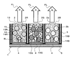
- FIG. 1 is a plan view showing a first embodiment of a full color LED display panel according to the present invention. It is an expanded sectional view which shows typically the principal part of FIG. It is sectional drawing explaining the electrical joining of the contact of LED of the full color LED display panel by this invention, and the electrode pad of a wiring board.
- 3 is a graph illustrating an emission spectrum of a red fluorescent light emitting layer of a full color LED display panel according to the present invention.
- 4 is a table illustrating color purity of a red fluorescent light emitting layer of a full color LED display panel according to the present invention. It is explanatory drawing which shows the LED array substrate manufacturing process in the manufacturing method of the said 1st Embodiment.
- FIG. 1 is a plan view showing a first embodiment of a full color LED display panel according to the present invention
- FIG. 2 is an enlarged cross-sectional view of a main part of FIG.
- This full-color LED display panel displays an image in color, and includes an LED array substrate 1, a fluorescent light emitting layer 2, and a light shielding member 3.
- the LED array substrate 1 is provided with a plurality of LEDs 4 arranged in a matrix as shown in FIG. 1, and a driving signal is supplied to each LED 4 from an external driving circuit, and each LED 4 is individually supplied.
- the plurality of LEDs 4 are arranged on a wiring substrate 5 (see FIG. 2) including a TFT driving substrate and a flexible substrate on which wiring for turning on and off to turn on and off is provided.
- a plurality of LEDs 4 are provided on the wiring board 5 as shown in FIG.
- the LED 4 emits light in the ultraviolet or blue wavelength band, and is manufactured using gallium nitride (GaN) as a main material.
- GaN gallium nitride
- An LED that emits near ultraviolet light having a wavelength of, for example, 200 nm to 380 nm, or an LED that emits blue light having a wavelength of, for example, 380 to 500 nm may be used.
- “upper” means the display surface side regardless of the installation state of the full-color LED display panel.
- the LED 4 has an electrical connection between the contact 8 of the LED 4 and the electrode pad 6 through a conductive elastic protrusion 7 formed by patterning on the electrode pad 6 of the wiring substrate 5. It has come to be.
- the elastic protrusion 7 is made of a resin-made protrusion 10 having a conductive film 9 such as gold or aluminum deposited on its surface, or conductive fine particles such as silver added to the photoresist.
- the protrusion 10 is formed of a conductive photoresist or a conductive photoresist containing a conductive polymer.
- the case where the protrusion 10 having the conductor film 9 deposited on the surface is formed as the elastic protrusion 7, but the elastic protrusion 7 is formed of a conductive photoresist. It may be.
- the LED 4 is bonded and fixed to the wiring board 5 via an adhesive layer 11 provided around the electrode pad 6 of the wiring board 5.
- the adhesive layer 11 is preferably a photosensitive adhesive that can be patterned by exposure and development. Alternatively, it may be an underfill agent or an ultraviolet curable adhesive.
- a fluorescent light emitting layer 2 is provided as shown in FIG.
- the fluorescent light emitting layer 2 is excited by the excitation light EL emitted from the LED 4 and converts the wavelength of the fluorescent light into the corresponding fluorescent light FL.
- the fluorescent light emitting layer 2 is arranged on each LED 4 corresponding to the three primary colors of red, green, and blue.
- Fluorescent resist having a corresponding color fluorescent pigment (pigment or dye) 14 uniformly dispersed in the provided red fluorescent light emitting layer 2R, green fluorescent light emitting layer 2G and blue fluorescent light emitting layer 2B is exposed and developed by photolithography. It has the shape of the island pattern formed.
- FIG. 1 shows the case where the fluorescent light-emitting layers 2 corresponding to the respective colors are provided in a stripe shape, they may be provided corresponding to each LED 4 individually.
- the fluorescent light-emitting layer 2 selectively selects light having a particle diameter on the order of several ⁇ m in the resist film 13 and light having a particle diameter on the order of several tens of nm and having a predetermined wavelength band.
- the adjustment dye 15 that permeates through and uniformly mixed and dispersed.
- the adjustment dye 15 transmits the excitation light EL emitted from the LED 4 and transmits light in the wavelength bands corresponding to the three primary colors among the fluorescence FL emitted when the fluorescent dye 14 is excited.
- pigments or dyes for color filters can be used. That is, as shown in FIG. 2, the red fluorescent light emitting layer 2R includes the red fluorescent dye 14R and the red adjusting dye 15R, and the green fluorescent light emitting layer 2G includes the green fluorescent dye 14G and the green adjusting dye 15G.
- the blue fluorescent light emitting layer 2B includes a blue fluorescent dye 14B and a blue adjusting dye 15B.
- FIG. 4 exemplifies the emission spectrum of the red fluorescent light emitting layer 2R containing the red fluorescent dye 14R and the red corresponding red adjusting dye 15R.
- the broken line indicates the transmission spectrum of the red adjusting dye 15R, and the alternate long and short dash line indicates the red color.
- the emission spectrum of the fluorescent dye 14R is shown, and the solid line shows the emission spectrum of the red fluorescent light emitting layer 2R containing the red adjusting dye 15R and the red fluorescent dye 14R.
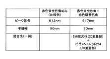
- FIG. 5 is a table showing the color purity of the red fluorescent light emitting layer 2R in comparison with the case of only the red fluorescent dye 14R.
- the red fluorescent dye 14R used here is an (Mg, Ca, Sr, Ba) 2 Si 5 N 8 : Eu phosphor (hereinafter referred to as “258 phosphor”), and the red adjusting dye 15R is a pigment red 254 ( Pigment Red 254).
- the mixing ratio of the 258 phosphor is 20 parts by weight and the pigment red 254 is 80 parts by weight.
- the above shows an example and is not limited to this.
- the emission characteristics of the red fluorescent light-emitting layer 2R containing the red fluorescent dye 14R and the red adjusting dye 15R were an emission peak of 617 nm and a half-value width of 70 nm.
- the emission peak was 612 nm, and the half width was 90 nm.
- the emission peak is shifted to the long wavelength side and the half width is also larger than when only the red fluorescent dye 14R is used. It can be seen that the color purity is improved by decreasing.
- a light shielding member 3 is provided so as to be attached to the peripheral surface 2 b except the light emitting surface 2 a of the fluorescent light emitting layer 2.
- the light shielding member 3 reflects or absorbs the excitation light EL and the fluorescence FL.
- a metal film such as aluminum or nickel that reflects the excitation light EL and the fluorescence FL is formed by sputtering or plating.
- coat for example, a black resist which absorbs excitation light EL and fluorescence FL so that the clearance gap between the adjacent fluorescence light emitting layers 2 may be filled.
- the light shielding member 3 attached to the light emitting surface 2a of the fluorescent light emitting layer 2 is later removed by various methods such as photolithography, laser irradiation, or polishing.
- the excitation light EL traveling obliquely in the direction of the adjacent fluorescent light emitting layer 2 in the fluorescent light emitting layer 2 is reflected by the metal film to the inside of the fluorescent light emitting layer 2. It can be used for excitation of the fluorescent dye 14, and the luminous efficiency of the fluorescent light emitting layer 2 can be improved. Further, since the fluorescent FL traveling obliquely in the fluorescent light emitting layer 2 is reflected by the metal film and emitted from the light emitting surface 2a of the fluorescent light emitting layer 2, the light utilization rate can be improved.
- the manufacturing method of the first embodiment of the full color LED display panel according to the present invention is roughly divided into an LED array substrate manufacturing process, a fluorescent light emitting layer forming process, and a light shielding member forming process. Hereinafter, each process is demonstrated in order.
- FIG. 6 is an explanatory view showing the LED array substrate manufacturing process.
- conductive elastic protrusions 7 are formed corresponding to the electrode pads 6 on the wiring substrate 5. More specifically, after applying a photospacer resist on the entire surface of the wiring substrate 5, exposure is performed using a photomask, development is performed, and projections 10 are formed by patterning on the electrode pads 6. After that, a highly conductive conductor film 9 such as gold or aluminum is formed on the protrusion 10 and the electrode pad 6 in a state of being electrically connected to each other to form the elastic protrusion 7.
- a resist layer is formed on the peripheral portion except for the electrode pad 6 by photolithography before forming the conductor film 9, and the resist layer is dissolved with a solution after the conductor film 9 is formed. At the same time, the conductive film 9 on the resist layer is lifted off.
- the elastic protrusion 7 may be a protrusion 10 formed of a conductive photoresist in which conductive fine particles such as silver are added to a photoresist or a conductive photoresist containing a conductive polymer.
- the elastic protrusion 7 is formed as a protrusion 10 on the electrode pad 6 by applying a conductive photoresist to the entire upper surface of the wiring substrate 5 with a predetermined thickness, exposing it using a photomask, developing it. Patterning is formed.
- the elastic protrusion 7 can be formed by applying a photolithography process, it is possible to ensure high accuracy in position and shape, and the interval between the contacts 8 of the LED 4 is narrower than about 10 ⁇ m. However, it can be formed easily. Therefore, a high-definition full color LED display panel can be manufactured.
- the elastic protrusion 7 is elastically deformed and contacts the contact 8 of the LED 4 by pressing of the LED 4, even when a plurality of LEDs 4 are simultaneously pressed as will be described later, the contact 8 of each LED 4 is connected to the elastic protrusion. 7 can be reliably brought into contact with. Therefore, the production yield of the full color LED display panel can be improved.
- a plurality of light emitting ultraviolet or blue wavelength bands formed on the sapphire substrate 16 and arranged in a matrix at the same pitch as the pixel pitch of the LED display panel.
- the LEDs 4 are aligned with respect to the wiring board 5 so that the contacts 8 thereof coincide with the electrode pads 6 of the wiring board 5.
- the sapphire substrate 16 is pressed against the wiring substrate 5, and the contact 8 of the LED 4 is electrically connected to the electrode pad 6 of the wiring substrate 5. Thereafter, the LED 4 is bonded and fixed to the wiring board 5 with an adhesive (not shown).
- the lighting state of each LED 4 may be inspected by energizing the wiring board 5. And you may adhere
- the non-defective LED 4 is peeled from the sapphire substrate 16 by irradiating the non-defective LED 4 with the laser light L from the sapphire substrate 16 side.
- the LED array substrate 1 in which the plurality of LEDs 4 are arranged in a matrix on the wiring substrate 5 is completed.
- a spare non-defective LED 4 or LED row is assigned to a portion of the wiring board 5 where the LED 4 determined to be defective or the LED column including the LED 4 determined to be defective is missing.
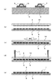
- FIG. 7 is an explanatory view showing a fluorescent light emitting layer forming step.
- a fluorescent resist 17 in which the fluorescent dye 14 and the adjusting dye 15 are uniformly dispersed in a transparent photosensitive resin is prepared.
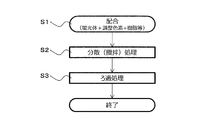
- the fluorescent resist 17 is manufactured by blending the fluorescent dye 14, the adjustment dye 15 and the transparent photosensitive resin at a predetermined ratio in step S1, and then in step S2, a stirrer. And the fluorescent dye 14 and the adjusting dye 15 are uniformly dispersed in the photosensitive resin.
- step S3 a filtering process is performed using a predetermined filter medium, and foreign matters such as gel foreign matters of the photosensitive resin are removed. In this way, the fluorescent resist 17 is manufactured.
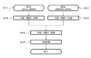
- step S11 after the fluorescent dye 14 is blended with a transparent photosensitive resin at a predetermined ratio in step S11, the mixture is stirred using a stirrer in step S12, and fluorescent in the photosensitive resin.
- the dye 14 is uniformly dispersed.
- step S13 after adjusting dye 15 is blended in an organic solvent at a predetermined ratio, the adjusting dye 15 is uniformly dispersed in the organic solvent by stirring using a stirrer in step S14.
- step S15 the fluorescent dye 14 dispersed in the photosensitive resin and the adjustment dye 15 dispersed in the organic solvent are mixed and then stirred, and the fluorescent dye 14 and the adjustment dye 15 are mixed in the photosensitive resin. And uniformly disperse.
- step S16 filtration is performed in step S16 to remove foreign matters such as gel-like foreign matters of the photosensitive resin.
- the fluorescent resist 17 may be manufactured.
- the well-known manufacturing process of a color resist can be applied to a stirring process, a filtration process, etc.
- a fluorescent light emitting layer forming process using the fluorescent resist 17 manufactured as described above will be described.
- a red fluorescent resist 17 is spin-coated or sprayed on the LED array substrate 1, for example.
- the red fluorescent resist 17 on the red LED 4 is exposed using a photomask 18.
- the green and blue fluorescent resists 17 are subjected to a coating process on the LED array substrate 1 and a photolithography process using a photomask 18, and as shown in FIG.
- a green fluorescent light emitting layer 2G and a blue fluorescent light emitting layer 2B are formed on the corresponding LED 4, respectively.
- FIG. 10 is an explanatory view showing a light shielding member forming step.
- a film is formed by sputtering or the like from the light emitting surface 2a side of the fluorescent light emitting layer 2, and aluminum or nickel as a light shielding member 3 is formed on the peripheral surface 2b of the fluorescent light emitting layer 2.
- a metal film is formed with a predetermined thickness.
- the light shielding member 3 may be formed by electroless plating of a metal film.
- a photosensitive black resist is applied on the fluorescent light emitting layer 2 and then cured by ultraviolet curing, for example. The gaps between them may be filled with the black resist.
- the light shielding member 3 on the light emitting surface 2a of the fluorescent light emitting layer 2 is removed by, for example, etching by photolithography, laser irradiation or polishing.
- a laser having a wavelength of about 260 nm to about 360 nm may be used.
- laser ablation may be performed using a laser having a wavelength of about 355 nm or more.
- the full color LED display panel according to the first embodiment of the present invention is formed by forming a transparent protective layer that transmits visible light (not shown) and an antireflection film that prevents reflection of external light on the display surface side surface.
- a transparent protective layer that transmits visible light (not shown) and an antireflection film that prevents reflection of external light on the display surface side surface.
- the blue fluorescent light emitting layer 2B may be omitted. Or you may provide what disperse
- FIG. 11 is an enlarged cross-sectional view showing a main part of a second embodiment of the full color LED display panel according to the present invention.
- the difference of the second embodiment from the first embodiment is that the fluorescent light emitting layer 2 and the light shielding member 3 are formed on another transparent substrate 19 different from the LED array substrate 1.
- the manufacturing method of the second embodiment will be described.
- the manufacturing method of the second embodiment is roughly divided into an LED array substrate manufacturing process, a fluorescent light emitting layer array substrate manufacturing process, and an assembly process.
- the LED array substrate manufacturing process is the same as the manufacturing method of the first embodiment, and a description thereof is omitted here.
- FIG. 12 is an explanatory view showing a fluorescent light emitting layer array substrate manufacturing process.
- a red fluorescent resist 17 is applied, for example, by spin coating or spray coating on a transparent substrate 19 made of, for example, glass or resin that transmits the excitation light EL and visible light.
- a red fluorescent resist 17 is exposed using a photomask 18.
- the island pattern of the red fluorescent resist 17 remains as shown in FIG. 12C, and the pitch is the same as the arrangement pitch of the LEDs 4 corresponding to red.
- a red fluorescent light emitting layer 2R is formed.
- the green and blue fluorescent resists 17 are subjected to a coating process on the transparent substrate 19 and a photolithography process using the photomask 18, and as shown in FIG.
- the green fluorescent light emitting layer 2G and the blue fluorescent light emitting layer 2B are formed at the same pitch as the arrangement pitch of the LEDs 4 respectively.
- a film is formed by sputtering or the like from the light emitting surface 2 a side of the fluorescent light emitting layer 2, and a metal such as aluminum or nickel as the light shielding member 3 on the side surface of the fluorescent light emitting layer 2.
- a film is formed with a predetermined thickness.
- the light shielding member 3 may be formed by electroless plating of a metal film.
- a photosensitive black resist is applied on the fluorescent light emitting layer 2 and then cured by ultraviolet curing, for example. The gaps between them may be filled with the black resist.
- the light shielding member 3 on the light emitting surface 2 a of the fluorescent light emitting layer 2 is removed by, for example, etching by photolithography, laser irradiation or polishing. In this manner, the fluorescent light emitting layer array substrate 20 having the light shielding member 3 on the peripheral surface 2b excluding the light emitting surface 2a of the fluorescent light emitting layer 2 is manufactured.
- FIG. 13 is an explanatory view showing the assembly process.
- a fluorescent light emitting layer array substrate 20 is installed on the LED array substrate 1, and an alignment mark (not shown) provided in advance on the LED array substrate 1 and the fluorescent light emitting layer array substrate 20 are provided.
- Each fluorescent light emitting layer 2 of the fluorescent light emitting layer array substrate 20 is positioned on each LED 4 of the LED array substrate 1 by using an alignment mark (not shown) provided in advance.
- both the substrates are pressure-bonded while maintaining the alignment state, and bonded by an adhesive (not shown).
- an adhesive not shown.
- the protective layer and the antireflection film may be formed on the fluorescent light emitting layer 2 after the fluorescent light emitting layer array substrate 20 is formed or after the assembly process is completed.
- the case where the light shielding member 3 is provided by being attached to the peripheral surface 2b except the light emitting surface 2a of the fluorescent light emitting layer 2 formed as an island pattern of the fluorescent resist 17 has been described.
- the invention is not limited to this, and as shown in FIGS. 14 (a) and 14 (b), a region surrounded by a partition wall 21 formed by patterning with a transparent photosensitive resin and having a light shielding member 3 attached to the surface.
- the fluorescent light emitting layer 2 may be formed by filling a fluorescent resist 17 having the fluorescent dye 14 and the adjusting dye 15 uniformly dispersed therein.
- the fluorescent resist 17 having the fluorescent dye 14 and the adjustment dye 15 dispersed uniformly is filled in the region surrounded by the black matrix 22 formed by patterning the black resist. What formed the fluorescent light emitting layer 2 may be used.
- the LED 4 is a light emitting diode whose main material is gallium nitride (GaN) has been described, but the present invention is not limited to this, and the LED 4 includes an organic EL. Therefore, the LED 4 of the LED array substrate 1 may be formed of an organic EL light emitting layer that emits light in the ultraviolet or blue wavelength band.
- GaN gallium nitride
Landscapes
- Physics & Mathematics (AREA)
- Engineering & Computer Science (AREA)
- General Physics & Mathematics (AREA)
- Optics & Photonics (AREA)
- Theoretical Computer Science (AREA)
- Microelectronics & Electronic Packaging (AREA)
- Electroluminescent Light Sources (AREA)
- Devices For Indicating Variable Information By Combining Individual Elements (AREA)
- Led Device Packages (AREA)
- Manufacturing & Machinery (AREA)
- Optical Filters (AREA)
Abstract
本発明は、紫外又は青色波長帯の光を放射する複数のLED4を配線基板5上にマトリクス状に配置したLEDアレイ基板1と、三色対応の複数の前記LED4上に、蛍光色素14及び予め定められた波長帯の光を選択的に透過する調整色素15を均一に分散させて有し、前記LED4から放射される励起光ELによって励起されて対応色の蛍光FLに波長変換する複数の蛍光発光層2と、複数の前記蛍光発光層2間に設けられ、前記励起光EL及び前記蛍光FLを反射又は吸収する遮光部材3と、を備えたものである。これにより、製造工程を短縮すると共に、蛍光発光層の厚みの増加を抑制する。
Description
本発明は、蛍光発光層を備えたフルカラーLED表示パネルに関し、特に製造工程を短縮すると共に、蛍光発光層の厚みの増加を抑制し得るフルカラーLED表示パネル及びその製造方法に係るものである。
従来のフルカラーLED表示パネルは、青色又は青緑色の光を放出する複数の有機EL素子を設けた有機EL素子基板上に、赤色対応の有機EL素子に対応させて赤色蛍光体層と赤色カラーフィルターとを積層し、緑色対応の有機EL素子に対応させて緑色蛍光体層と緑色カラーフィルターとを積層し、青色対応の有機EL素子に対応させて青色カラーフィルターを設けた色変換基板を配置した構成となっていた(例えば、特許文献1参照)。
しかし、このような従来のフルカラーLED表示パネルにおいては、蛍光体層とカラーフィルターとを積層して色変換基板を形成するものであるため、製造工程が増して製造コストが高くなるという問題がある。
また、色変換基板の層厚が厚くなって剛性がまし、例えばフレキシブルなディスプレイパネルにおける可撓性が失われるというおそれがある。
そこで、本発明は、このような問題点に対処し、製造工程を短縮すると共に、蛍光発光層の厚みの増加を抑制し得るフルカラーLED表示パネル及びその製造方法を提供することを目的とする。
上記目的を達成するために、本発明によるフルカラーLED表示パネルは、紫外又は青色波長帯の光を放射する複数のLEDを配線基板上にマトリクス状に配置したLEDアレイ基板と、三色対応の複数の前記LED上に、蛍光色素及び予め定められた波長帯の光を選択的に透過する調整色素を均一に分散させて有し、前記LEDから放射される励起光によって励起されて対応色の蛍光に波長変換する複数の蛍光発光層と、複数の前記蛍光発光層間に設けられ、前記励起光及び前記蛍光を反射又は吸収する遮光部材と、を備えたものである。
また、本発明によるフルカラーLED表示パネルの製造方法は、紫外又は青色波長帯の光を放射する複数のLEDを配線基板上にマトリクス状に配置してLEDアレイ基板を形成する第1ステップと、三色対応の複数の前記LED上に、蛍光色素及び予め定められた波長帯の光を選択的に透過する調整色素を均一に分散させて有し、前記LEDから放射される励起光によって励起されて対応色の蛍光に波長変換する複数の蛍光発光層を形成する第2ステップと、複数の前記蛍光発光層間に前記励起光及び前記蛍光を反射又は吸収する遮光部材を設ける第3ステップと、を含むものである。
本発明によれば、蛍光発光層が蛍光色素及び予め定められた波長帯の光を選択的に透過する調整色素を均一に分散させて有するものであるため、従来技術と違って、カラーフィルターの形成工程を省略することができ、製造工程を短縮することができる。したがって、フルカラーLED表示パネルの製造コストを低減することができる。また、従来技術におけるようなカラーフィルターの層が存在しないため蛍光発光層の層厚が薄くなり、例えばフレキシブルなディスプレイパネルの可撓性を損なうおそれがない。
以下、本発明の実施形態を添付図面に基づいて詳細に説明する。図1は本発明によるフルカラーLED表示パネルの第1の実施形態を示す平面図であり、図2は、図1の要部拡大断面図である。このフルカラーLED表示パネルは、映像をカラー表示するもので、LEDアレイ基板1と、蛍光発光層2と、遮光部材3と、を備えて構成されている。
上記LEDアレイ基板1は、図1に示すように複数のLED4をマトリクス状に配置して備えたものであり、外部に設けた駆動回路から駆動信号を各LED4に供給し、各LED4を個別にオン及びオフ駆動して点灯及び消灯させるための配線を設けたTFT駆動基板及びフレキシブル基板等を含む配線基板5(図2を参照)上に、上記複数のLED4を配置したものとなっている。
上記配線基板5上には、図2に示すように複数のLED4が設けられている。このLED4は、紫外又は青色波長帯の光を発光するものであり、窒化ガリウム(GaN)を主材料として製造される。なお、波長が例えば200nm~380nmの近紫外線を発光するLEDであっても、波長が例えば380nm~500nmの青色光を発光するLEDであってもよい。なお、本明細書において、「上」は、フルカラーLED表示パネルの設置状態に関わらず、表示面側を言う。
詳細には、図3に示すように、LED4は、配線基板5の電極パッド6上にパターニング形成された導電性の弾性突起部7を介してLED4の接点8と上記電極パッド6とが電気接続されるようになっている。
より詳細には、上記弾性突起部7は、表面に金やアルミニウム等の良導電性の導電体膜9を被着させた樹脂製の突起10や、フォトレジストに銀等の導電性微粒子を添加した導電性フォトレジスト又は導電性高分子を含む導電性フォトレジストで形成した突起10である。なお、図3においては、一例として弾性突起部7として表面に導電体膜9を被着させた突起10を形成した場合を示しているが、弾性突起部7は導電性フォトレジストで形成したものであってもよい。
さらに、図3に示すように、LED4は、配線基板5の電極パッド6の周囲に設けられた接着剤層11を介して配線基板5に接着固定されている。この場合、上記接着剤層11は、露光及び現像によりパターニングが可能な感光性接着剤であるとよい。又は、アンダーフィル剤であっても、紫外線硬化型の接着剤であってもよい。
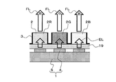
上記LEDアレイ基板1の各LED4上には、図2に示すように蛍光発光層2が設けられている。この蛍光発光層2は、LED4から放射される励起光ELによって励起されて対応色の蛍光FLに夫々波長変換するものであり、赤、緑、青の光三原色に対応させて各LED4上に並べて設けられた赤色蛍光発光層2R、緑色蛍光発光層2G及び青色蛍光発光層2Bで、対応色の蛍光色素(顔料又は染料)14を均一に分散させて有する蛍光レジストをフォトリソグラフィーにより露光及び現像して形成された島パターンの形状を有するものである。なお、図1においては、各色対応の蛍光発光層2をストライプ状に設けた場合について示しているが、各LED4に個別に対応させて設けてもよい。
詳細には、上記蛍光発光層2は、レジスト膜13中に数μmオーダーの粒子径を有する蛍光色素14と、数10nmオーダーの粒子径を有し、予め定められた波長帯の光を選択的に透過する調整色素15とを均一に混合、分散させて含有するものである。
より詳細には、上記調整色素15は、LED4から発せられる励起光ELを透過すると共に、蛍光色素14が励起されて発する蛍光FLのうち、三原色に対応する波長帯の光を透過し、それ以外の不要な波長の光を吸収するもので、カラーフィルター用の顔料又は染料を使用することができる。即ち、図2に示すように、赤色蛍光発光層2Rには、赤色蛍光色素14Rと赤色調整色素15Rとが含まれ、緑色蛍光発光層2Gには、緑色蛍光色素14Gと緑色調整色素15Gとが含まれ、青色蛍光発光層2Bには、青色蛍光色素14Bと青色調整色素15Bとが含まれている。
図4は赤色の蛍光色素14Rと赤色対応の赤色調整色素15Rを含有する赤色蛍光発光層2Rの発光スペクトルを例示したものであり、破線は赤色調整色素15Rの透過スペクトルを示し、一点鎖線は赤色蛍光色素14Rの発光スペクトルを示し、実線は上記赤色調整色素15R及び赤色蛍光色素14Rを含有する赤色蛍光発光層2Rの発光スペクトルを示している。また、図5は上記赤色蛍光発光層2Rの色純度を赤色蛍光色素14Rのみの場合と比較して示す表である。ここで使用した赤色蛍光色素14Rは(Mg,Ca,Sr,Ba)2Si5N8:Eu蛍光体(以下、「258蛍光体」という)であり、赤色調整色素15Rは、ピグメントレッド254(Pigment Red 254)である。そして、その混合比は、258蛍光体が20重量部、ピグメントレッド254が80重量部となっている。なお、以上は、一例を示すものであり、これに限定されない。
図5に示すように、赤色蛍光色素14Rと赤色調整色素15Rとを含有する赤色蛍光発光層2Rの発光特性は、発光ピークが617nm、半値幅が70nmであった。一方、赤色蛍光色素14Rのみの発光特性は、発光ピークが612nm、半値幅が90nmであった。このように、赤色蛍光色素14Rと赤色調整色素15Rとを含有する赤色蛍光発光層2Rは、赤色蛍光色素14Rのみを使用した場合に比べて、発光ピークが長波長側にシフトし、半値幅も小さくなって色純度が向上していることが分かる。
図2に示すように、上記蛍光発光層2の光放出面2aを除く周面2bに被着させて遮光部材3が設けられている。この遮光部材3は、励起光EL及び蛍光FLを反射又は吸収するもので、例えば、励起光EL及び蛍光FLを反射するアルミニウムやニッケル等の金属膜をスパッタリングやめっき等により形成したものである。又は、隣接する蛍光発光層2の間の隙間を埋めるように励起光EL及び蛍光FLを吸収する、例えば黒色レジストを塗布して設けてもよい。なお、蛍光発光層2の光放出面2aに被着した遮光部材3は、後にフォトリソグラフィー、レーザ照射又は研磨等の種々の手法により除去される。
上記遮光部材3として金属膜が使用される場合には、蛍光発光層2内を隣接する蛍光発光層2の方向に斜めに進む励起光ELを金属膜により蛍光発光層2の内側に反射して蛍光色素14の励起に使用することができ、蛍光発光層2の発光効率を向上することができる。また、蛍光発光層2内を斜めに進む蛍光FLは、金属膜により反射されて蛍光発光層2の光放出面2aから放出されるため、光利用率の向上を図ることもできる。
次に、このように構成されたフルカラーLED表示パネルの第1の実施形態の製造方法について説明する。
本発明によるフルカラーLED表示パネルの第1の実施形態の製造方法は、大別して、LEDアレイ基板製造工程と、蛍光発光層形成工程と、遮光部材形成工程とに分けられる。以下、各工程について順番に説明する。
本発明によるフルカラーLED表示パネルの第1の実施形態の製造方法は、大別して、LEDアレイ基板製造工程と、蛍光発光層形成工程と、遮光部材形成工程とに分けられる。以下、各工程について順番に説明する。
(LEDアレイ基板製造工程)
図6はLEDアレイ基板製造工程を示す説明図である。
先ず、図6(a)に示すように、配線基板5上の電極パッド6に対応して、導電性の弾性突起部7が形成される。詳細には、配線基板5の全面にフォトスペーサ用のレジストを塗布したのち、フォトマスクを使用して露光し、現像して電極パッド6上に突起10をパターニング形成する。その後、上記突起10及び電極パッド6上に、互いに導通させた状態で金又はアルミニウム等の良導電性の導電体膜9をスパッタリングや蒸着等により成膜して弾性突起部7を形成する。
図6はLEDアレイ基板製造工程を示す説明図である。
先ず、図6(a)に示すように、配線基板5上の電極パッド6に対応して、導電性の弾性突起部7が形成される。詳細には、配線基板5の全面にフォトスペーサ用のレジストを塗布したのち、フォトマスクを使用して露光し、現像して電極パッド6上に突起10をパターニング形成する。その後、上記突起10及び電極パッド6上に、互いに導通させた状態で金又はアルミニウム等の良導電性の導電体膜9をスパッタリングや蒸着等により成膜して弾性突起部7を形成する。
より詳細には、導電体膜9を成膜する前に、フォトリソグラフィーにより電極パッド6上を除く周辺部分にレジスト層を形成し、導電体膜9の成膜後に溶解液でレジスト層を溶解させると共に、レジスト層上の導電体膜9をリフトオフする。
なお、弾性突起部7は、フォトレジストに銀等の導電性微粒子を添加した導電性フォトレジスト又は導電性高分子を含む導電性フォトレジストで形成した突起10であってもよい。この場合は、弾性突起部7は、配線基板5の上面の全面に導電性フォトレジストを所定厚みで塗布したのち、フォトマスクを使用して露光し、現像して電極パッド6上に突起10としてパターニング形成される。
このように、上記弾性突起部7は、フォトリソグラフィープロセスを適用して形成することができるので、位置及び形状に高い精度を確保することができ、LED4の接点8の間隔が10μm程度より狭くなっても容易に形成することができる。したがって、高精細なフルカラーLED表示パネルの製造が可能となる。
また、弾性突起部7は、LED4の押圧によりLED4の接点8に弾性変形して接触するので、後述するように複数のLED4を同時に押圧した場合にも、各LED4の各接点8を弾性突起部7に確実に接触させることができる。したがって、フルカラーLED表示パネルの製造歩留りを向上することができる。
次に、図6(b)に示すように、例えばサファイア基板16上にLED表示パネルの画素ピッチと同じピッチでマトリクス状に配置して形成された、紫外又は青色波長帯の光を放射する複数のLED4が、その接点8が上記配線基板5の電極パッド6に合致するように配線基板5に対してアライメントされる。
次いで、図6(c)に示すように、サファイア基板16が配線基板5に対して圧着され、LED4の接点8が配線基板5の電極パッド6に電気的に接続される。その後、図示省略の接着剤によりLED4が配線基板5に接着固定される。この場合、LED4を配線基板5に接着固定する前に、配線基板5に通電して各LED4の点灯状態を検査してもよい。そして、点灯不良と判定されたLED4又は該不良判定のLED4を含むLED列を除く良品のLED4のみを接着してもよい。
続いて、図6(d)に示すように、サファイア基板16側から良品のLED4に対してレーザ光Lを照射して良品のLED4をサファイア基板16から剥離する。これにより、図6(e)に示すように、複数のLED4を配線基板5上にマトリクス状に配置したLEDアレイ基板1が完成する。なお、配線基板5上の、不良と判定されたLED4又は該不良判定のLED4を含むLED列の抜けた部分には、予備の良品のLED4又はLED列があてがわれる。
(蛍光発光層形成工程)
図7は蛍光発光層形成工程を示す説明図である。
先ず、蛍光発光層形成工程を実施する前に、蛍光色素14と調整色素15とを透明な感光性樹脂中に均一に分散させた蛍光レジスト17が準備される。このような蛍光レジスト17の製法は、例えば図8に示すように、ステップS1において、蛍光色素14と調整色素15と透明な感光性樹脂とを所定の比率で配合した後、ステップS2において、攪拌機を使用して撹拌処理し、感光性樹脂中に蛍光色素14と調整色素15とを均一に分散させる。その後、ステップS3において、所定のろ過材を使用してろ過処理を実施し、例えば感光性樹脂のゲル状異物等の異物が除去される。このようにして、蛍光レジスト17が製造される。
図7は蛍光発光層形成工程を示す説明図である。
先ず、蛍光発光層形成工程を実施する前に、蛍光色素14と調整色素15とを透明な感光性樹脂中に均一に分散させた蛍光レジスト17が準備される。このような蛍光レジスト17の製法は、例えば図8に示すように、ステップS1において、蛍光色素14と調整色素15と透明な感光性樹脂とを所定の比率で配合した後、ステップS2において、攪拌機を使用して撹拌処理し、感光性樹脂中に蛍光色素14と調整色素15とを均一に分散させる。その後、ステップS3において、所定のろ過材を使用してろ過処理を実施し、例えば感光性樹脂のゲル状異物等の異物が除去される。このようにして、蛍光レジスト17が製造される。
又は、図9に示すように、ステップS11において、蛍光色素14を透明な感光性樹脂に所定の比率で配合した後、ステップS12において、攪拌機を使用して撹拌処理し、感光性樹脂中に蛍光色素14を均一に分散させる。一方、ステップS13においては、調整色素15を有機溶剤に所定の比率で配合した後、ステップS14において攪拌機を使用して撹拌処理し、有機溶剤中に調整色素15を均一に分散させる。そして、ステップS15において、感光性樹脂中に分散させた蛍光色素14と有機溶剤中に分散させた調整色素15とを混合した後、撹拌処理し、感光性樹脂中に蛍光色素14と調整色素15とを均一に分散させる。その後、ステップS16においてろ過処理し、例えば感光性樹脂のゲル状異物等の異物が除去される。このようにして、蛍光レジスト17を製造してもよい。なお、撹拌処理やろ過処理等は、カラーレジストの公知の製造工程を適用することができる。
次に、上記のようにして製造された蛍光レジスト17を使用する蛍光発光層形成工程について説明する。
先ず、図7(a)に示すように、LEDアレイ基板1上に例えば赤色の蛍光レジスト17が例えばスピンコート又はスプレー塗布される。
先ず、図7(a)に示すように、LEDアレイ基板1上に例えば赤色の蛍光レジスト17が例えばスピンコート又はスプレー塗布される。
次に、図7(b)に示すように、フォトマスク18を使用して赤色対応のLED4上の赤色の蛍光レジスト17が露光される。
次いで、上記赤色の蛍光レジスト17を所定の現像液により現像することにより、図7(c)に示すように赤色対応のLED4上に赤色の蛍光レジスト17の島パターンが残り、赤色蛍光発光層2Rが形成される。
その後、同様にして、緑色及び青色の蛍光レジスト17について、LEDアレイ基板1上への塗布工程及びフォトマスク18を使用したフォトリソグラフィー工程を経て、図7(d)に示すように、緑色及び青色対応のLED4上に夫々緑色蛍光発光層2G及び青色蛍光発光層2Bが形成される。
(遮光部材形成工程)
図10は遮光部材形成工程を示す説明図である。
先ず、図10(a)に示すように、蛍光発光層2の光放出面2a側からスパッタリング等により成膜して、蛍光発光層2の周面2bに遮光部材3としてのアルミニウムやニッケル等の金属膜を所定厚みで形成する。この場合、遮光部材3は、金属膜を無電解めっきにより形成してもよいし、例えば蛍光発光層2上に例えば感光性の黒色レジストを塗布した後、紫外線硬化させて隣接する蛍光発光層2の間の隙間を上記黒色レジストにより埋めてもよい。
図10は遮光部材形成工程を示す説明図である。
先ず、図10(a)に示すように、蛍光発光層2の光放出面2a側からスパッタリング等により成膜して、蛍光発光層2の周面2bに遮光部材3としてのアルミニウムやニッケル等の金属膜を所定厚みで形成する。この場合、遮光部材3は、金属膜を無電解めっきにより形成してもよいし、例えば蛍光発光層2上に例えば感光性の黒色レジストを塗布した後、紫外線硬化させて隣接する蛍光発光層2の間の隙間を上記黒色レジストにより埋めてもよい。
次に、図10(b)に示すように、蛍光発光層2の光放出面2a上の遮光部材3を、例えばフォトリソグラフィーによるエッチング、レーザ照射又は研磨により除去する。レーザ照射により金属膜を除去する場合には、約260nm~約360nmの波長のレーザを使用するとよい。また、レーザ照射により黒色レジストを除去する場合には、約355nm以上の波長のレーザを使用してレーザアブレーションするとよい。
その後、表示面側表面に図示省略の可視光を透過する透明な保護層及び外光の反射を防止する反射防止膜を形成することにより、第1の実施形態による本発明のフルカラーLED表示パネルが完成する。なお、LED4が青色光を発光するものである場合には、青色蛍光発光層2Bは無くてもよい。又は、レジスト膜13中に青色調整色素15Bのみを分散させたものを設けてもよい。
図11は本発明によるフルカラーLED表示パネルの第2の実施形態を示す要部拡大断面図である。
第2の実施形態の第1の実施形態と異なる点は、蛍光発光層2及び遮光部材3がLEDアレイ基板1とは異なる別の透明基板19上に形成されているということである。以下、第2の実施形態の製造方法について説明する。
第2の実施形態の第1の実施形態と異なる点は、蛍光発光層2及び遮光部材3がLEDアレイ基板1とは異なる別の透明基板19上に形成されているということである。以下、第2の実施形態の製造方法について説明する。
第2の実施形態の製造方法は、大別して、LEDアレイ基板製造工程と、蛍光発光層アレイ基板製造工程と、組立工程とに分けられる。
上記LEDアレイ基板製造工程は、第1の実施形態の製造方法と同じであり、ここでは説明を省略する。
上記LEDアレイ基板製造工程は、第1の実施形態の製造方法と同じであり、ここでは説明を省略する。
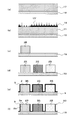
図12は蛍光発光層アレイ基板製造工程を示す説明図である。
先ず、図12(a)に示すように、励起光EL及び可視光を透過する例えばガラスや樹脂製の透明基板19上に例えば赤色の蛍光レジスト17が例えばスピンコート又はスプレー塗布される。
先ず、図12(a)に示すように、励起光EL及び可視光を透過する例えばガラスや樹脂製の透明基板19上に例えば赤色の蛍光レジスト17が例えばスピンコート又はスプレー塗布される。
次に、図12(b)に示すように、フォトマスク18を使用して赤色の蛍光レジスト17が露光される。
次いで、上記赤色の蛍光レジスト17を所定の現像液により現像することにより、図12(c)に示すように赤色の蛍光レジスト17の島パターンが残り、赤色対応のLED4の配列ピッチと同じピッチで赤色蛍光発光層2Rが形成される。
その後、同様にして、緑色及び青色の蛍光レジスト17について、透明基板19上への塗布工程及びフォトマスク18を使用したフォトリソグラフィー工程を経て、図12(d)に示すように、緑色及び青色対応のLED4の配列ピッチと同じピッチで夫々緑色蛍光発光層2G及び青色蛍光発光層2Bが形成される。
次に、図12(e)に示すように、蛍光発光層2の光放出面2a側からスパッタリング等により成膜して、蛍光発光層2の側面に遮光部材3としてのアルミニウムやニッケル等の金属膜を所定厚みで形成する。この場合、遮光部材3は、金属膜を無電解めっきにより形成してもよいし、例えば蛍光発光層2上に例えば感光性の黒色レジストを塗布した後、紫外線硬化させて隣接する蛍光発光層2の間の隙間を上記黒色レジストにより埋めてもよい。
次いで、図12(f)に示すように、蛍光発光層2の光放出面2a上の遮光部材3を、例えばフォトリソグラフィーによるエッチング、レーザ照射又は研磨により除去する。このようにして、蛍光発光層2の光放出面2aを除く周面2bに遮光部材3を備えた蛍光発光層アレイ基板20が製造される。
図13は組立工程を示す説明図である。
先ず、図13(a)に示すように、LEDアレイ基板1上に蛍光発光層アレイ基板20が設置され、LEDアレイ基板1に予め設けられた図示省略のアライメントマークと蛍光発光層アレイ基板20に予め設けられた図示所略のアライメントマークとを使用してアライメントされ、LEDアレイ基板1の各LED4上に、蛍光発光層アレイ基板20の各蛍光発光層2が位置づけられる。
先ず、図13(a)に示すように、LEDアレイ基板1上に蛍光発光層アレイ基板20が設置され、LEDアレイ基板1に予め設けられた図示省略のアライメントマークと蛍光発光層アレイ基板20に予め設けられた図示所略のアライメントマークとを使用してアライメントされ、LEDアレイ基板1の各LED4上に、蛍光発光層アレイ基板20の各蛍光発光層2が位置づけられる。
次に、図13(b)に示すように、両基板は、アライメント状態が維持されたまま圧着され、図示省略の接着剤により接合される。これにより、本発明によるフルカラーLED表示パネルの第2の実施形態が完成する。なお、第1の実施形態と同様に、LED4が青色光を発光するものである場合には、青色蛍光発光層2Bは無くてもよいし、レジスト膜13中に青色調整色素15Bのみを分散させたものを設けてもよい。
上記第2の実施形態において、蛍光発光層2上への保護層及び反射防止膜の形成は、蛍光発光層アレイ基板20の形成後、又は上記組立工程の終了後に行ってもよい。
なお、上記実施形態においては、蛍光レジスト17の島パターンとして形成された蛍光発光層2の光放出面2aを除く周面2bに被着させて遮光部材3を設けた場合について説明したが、本発明はこれに限られず、図14(a),(b)に示すように、透明な感光性樹脂でパターニング形成され、表面に遮光部材3を被着させて設けた隔壁21によって囲まれた領域内に、蛍光色素14及び調整色素15を均一に分散させて有する蛍光レジスト17を充填して蛍光発光層2を形成したものであってもよい。又は、図14(c)に示すように、黒色レジストをパターニング形成したブラックマトリクス22によって囲まれた領域内に、蛍光色素14及び調整色素15を均一に分散させて有する蛍光レジスト17を充填して蛍光発光層2を形成したものであってもよい。
以上の説明においては、LED4が窒化ガリウム(GaN)を主材料とした発光ダイオードである場合について述べたが、本発明はこれに限られず、LED4は有機ELも含むものである。したがって、LEDアレイ基板1のLED4を紫外又は青色波長帯の光を放射する有機EL発光層で形成してもよい。
1…LEDアレイ基板
2…蛍光発光層
2a…光放出面
2b…周面
2R…赤色蛍光発光層
2G…緑色蛍光発光層
2B…青色蛍光発光層
3…遮光部材
4…LED
5…配線基板
14…蛍光色素
15…調整色素
17…蛍光レジスト
EL…励起光
FL…蛍光
2…蛍光発光層
2a…光放出面
2b…周面
2R…赤色蛍光発光層
2G…緑色蛍光発光層
2B…青色蛍光発光層
3…遮光部材
4…LED
5…配線基板
14…蛍光色素
15…調整色素
17…蛍光レジスト
EL…励起光
FL…蛍光
Claims (8)
- 紫外又は青色波長帯の光を放射する複数のLEDを配線基板上にマトリクス状に配置したLEDアレイ基板と、
三色対応の複数の前記LED上に、蛍光色素及び予め定められた波長帯の光を選択的に透過する調整色素を均一に分散させて有し、前記LEDから放射される励起光によって励起されて対応色の蛍光に波長変換する複数の蛍光発光層と、
複数の前記蛍光発光層間に設けられ、前記励起光及び前記蛍光を反射又は吸収する遮光部材と、
を備えたことを特徴とするフルカラーLED表示パネル。 - 前記蛍光発光層は、感光性樹脂に前記蛍光色素及び前記調整色素を均一に分散させて有する蛍光レジストの島パターンの形態を有していることを特徴とする請求項1記載のフルカラーLED表示パネル。
- 前記蛍光発光層の光放出面を除く周面に被着させて前記遮光部材が設けられていることを特徴とする請求項2記載のフルカラーLED表示パネル。
- 前記遮光部材は、前記励起光及び前記蛍光を反射する金属膜であることを特徴とする請求項1~3のいずれか1項に記載のフルカラーLED表示パネル。
- 紫外又は青色波長帯の光を放射する複数のLEDを配線基板上にマトリクス状に配置してLEDアレイ基板を形成する第1ステップと、
三色対応の複数の前記LED上に、蛍光色素及び予め定められた波長帯の光を選択的に透過する調整色素を均一に分散させて有し、前記LEDから放射される励起光によって励起されて対応色の蛍光に波長変換する複数の蛍光発光層を形成する第2ステップと、
複数の前記蛍光発光層間に前記励起光及び前記蛍光を反射又は吸収する遮光部材を設ける第3ステップと、
を含むことを特徴とするフルカラーLED表示パネルの製造方法。 - 前記第2ステップは、感光性樹脂に前記蛍光色素及び前記調整色素を均一に分散させて有する蛍光レジストを露光及び現像して、島パターンの形態を有する蛍光発光層を形成することを特徴とする請求項5記載のフルカラーLED表示パネルの製造方法。
- 前記第3ステップは、前記蛍光発光層の光放出面を除く周面に被着させて前記遮光部材を設けることを特徴とする請求項6記載のフルカラーLED表示パネルの製造方法。
- 前記遮光部材は、前記励起光及び前記蛍光を反射する金属膜であることを特徴とする請求項5~7のいずれか1項に記載のフルカラーLED表示パネルの製造方法。
Priority Applications (3)
| Application Number | Priority Date | Filing Date | Title |
|---|---|---|---|
| KR1020207023620A KR20200121313A (ko) | 2018-02-15 | 2019-01-31 | 풀 컬러 led 표시 패널 및 그 제조 방법 |
| CN201980013468.5A CN111712935A (zh) | 2018-02-15 | 2019-01-31 | 全彩led显示面板及其制造方法 |
| US16/993,498 US20200373350A1 (en) | 2018-02-15 | 2020-08-14 | Full-Color Led Display Panel And Method For Manufacturing Same |
Applications Claiming Priority (2)
| Application Number | Priority Date | Filing Date | Title |
|---|---|---|---|
| JP2018025313A JP2019140361A (ja) | 2018-02-15 | 2018-02-15 | フルカラーled表示パネル及びその製造方法 |
| JP2018-025313 | 2018-02-15 |
Related Child Applications (1)
| Application Number | Title | Priority Date | Filing Date |
|---|---|---|---|
| US16/993,498 Continuation US20200373350A1 (en) | 2018-02-15 | 2020-08-14 | Full-Color Led Display Panel And Method For Manufacturing Same |
Publications (1)
| Publication Number | Publication Date |
|---|---|
| WO2019159702A1 true WO2019159702A1 (ja) | 2019-08-22 |
Family
ID=67619074
Family Applications (1)
| Application Number | Title | Priority Date | Filing Date |
|---|---|---|---|
| PCT/JP2019/003452 Ceased WO2019159702A1 (ja) | 2018-02-15 | 2019-01-31 | フルカラーled表示パネル及びその製造方法 |
Country Status (6)
| Country | Link |
|---|---|
| US (1) | US20200373350A1 (ja) |
| JP (1) | JP2019140361A (ja) |
| KR (1) | KR20200121313A (ja) |
| CN (1) | CN111712935A (ja) |
| TW (1) | TW201941471A (ja) |
| WO (1) | WO2019159702A1 (ja) |
Cited By (2)
| Publication number | Priority date | Publication date | Assignee | Title |
|---|---|---|---|---|
| WO2022052310A1 (zh) * | 2020-09-09 | 2022-03-17 | 深圳市奥拓电子股份有限公司 | 一种紫外led激发荧光显示方法、装置和系统 |
| KR20240170532A (ko) | 2022-04-05 | 2024-12-03 | 도판 홀딩스 가부시키가이샤 | 표시 장치 및 파장 변환 기판 |
Families Citing this family (8)
| Publication number | Priority date | Publication date | Assignee | Title |
|---|---|---|---|---|
| JP2020085960A (ja) * | 2018-11-16 | 2020-06-04 | 株式会社ブイ・テクノロジー | フルカラーled表示パネル |
| JP7425618B2 (ja) * | 2020-02-10 | 2024-01-31 | アオイ電子株式会社 | 発光装置の製造方法、および発光装置 |
| WO2021221056A1 (ja) | 2020-05-01 | 2021-11-04 | ソニーセミコンダクタソリューションズ株式会社 | 表示装置および表面実装部品 |
| KR20220111513A (ko) | 2021-02-02 | 2022-08-09 | 삼성전자주식회사 | 디스플레이 모듈 및 그 제조 방법 |
| CN116848575A (zh) * | 2021-03-16 | 2023-10-03 | 谷歌有限责任公司 | 使用微型led和微型led阵列的群组的显示器制造方法 |
| WO2023070369A1 (zh) * | 2021-10-27 | 2023-05-04 | 重庆康佳光电技术研究院有限公司 | 一种微发光二极管显示器及其制作方法 |
| CN116190409B (zh) * | 2022-11-29 | 2025-05-30 | 厦门天马微电子有限公司 | 一种显示面板及其制备方法、显示装置 |
| JP7741521B2 (ja) * | 2023-06-16 | 2025-09-18 | シャープ株式会社 | 表示パネル |
Citations (7)
| Publication number | Priority date | Publication date | Assignee | Title |
|---|---|---|---|---|
| JP2010087224A (ja) * | 2008-09-30 | 2010-04-15 | Toyoda Gosei Co Ltd | Led表示装置およびled表示装置用隔壁の製造方法 |
| JP2013239431A (ja) * | 2012-04-20 | 2013-11-28 | Semiconductor Energy Lab Co Ltd | 発光素子、発光装置、表示装置、電子機器及び照明装置 |
| JP2013254651A (ja) * | 2012-06-07 | 2013-12-19 | Sharp Corp | 蛍光体基板、発光デバイス、表示装置、及び照明装置 |
| JP2016523450A (ja) * | 2013-06-18 | 2016-08-08 | ルクスビュー テクノロジー コーポレイション | 波長変換層を有するledディスプレイ |
| US20160320664A1 (en) * | 2015-04-30 | 2016-11-03 | Samsung Display Co., Ltd. | Liquid crystal display device and method for driving the same |
| JP2017510843A (ja) * | 2014-03-10 | 2017-04-13 | オスラム オプト セミコンダクターズ ゲゼルシャフト ミット ベシュレンクテル ハフツングOsram Opto Semiconductors GmbH | 波長変換素子、波長変換素子を含む発光半導体コンポーネント、波長変換素子の製造方法、および波長変換素子を含む発光半導体コンポーネントの製造方法 |
| US20170242292A1 (en) * | 2016-02-22 | 2017-08-24 | Samsung Display Co., Ltd. | Quantum dot color filter and display device including the same |
Family Cites Families (1)
| Publication number | Priority date | Publication date | Assignee | Title |
|---|---|---|---|---|
| JP2016164855A (ja) | 2015-03-06 | 2016-09-08 | シャープ株式会社 | 発光装置並びにこれを備えた表示装置、照明装置および電子機器 |
-
2018
- 2018-02-15 JP JP2018025313A patent/JP2019140361A/ja active Pending
-
2019
- 2019-01-31 KR KR1020207023620A patent/KR20200121313A/ko not_active Withdrawn
- 2019-01-31 CN CN201980013468.5A patent/CN111712935A/zh active Pending
- 2019-01-31 WO PCT/JP2019/003452 patent/WO2019159702A1/ja not_active Ceased
- 2019-02-13 TW TW108104718A patent/TW201941471A/zh unknown
-
2020
- 2020-08-14 US US16/993,498 patent/US20200373350A1/en not_active Abandoned
Patent Citations (7)
| Publication number | Priority date | Publication date | Assignee | Title |
|---|---|---|---|---|
| JP2010087224A (ja) * | 2008-09-30 | 2010-04-15 | Toyoda Gosei Co Ltd | Led表示装置およびled表示装置用隔壁の製造方法 |
| JP2013239431A (ja) * | 2012-04-20 | 2013-11-28 | Semiconductor Energy Lab Co Ltd | 発光素子、発光装置、表示装置、電子機器及び照明装置 |
| JP2013254651A (ja) * | 2012-06-07 | 2013-12-19 | Sharp Corp | 蛍光体基板、発光デバイス、表示装置、及び照明装置 |
| JP2016523450A (ja) * | 2013-06-18 | 2016-08-08 | ルクスビュー テクノロジー コーポレイション | 波長変換層を有するledディスプレイ |
| JP2017510843A (ja) * | 2014-03-10 | 2017-04-13 | オスラム オプト セミコンダクターズ ゲゼルシャフト ミット ベシュレンクテル ハフツングOsram Opto Semiconductors GmbH | 波長変換素子、波長変換素子を含む発光半導体コンポーネント、波長変換素子の製造方法、および波長変換素子を含む発光半導体コンポーネントの製造方法 |
| US20160320664A1 (en) * | 2015-04-30 | 2016-11-03 | Samsung Display Co., Ltd. | Liquid crystal display device and method for driving the same |
| US20170242292A1 (en) * | 2016-02-22 | 2017-08-24 | Samsung Display Co., Ltd. | Quantum dot color filter and display device including the same |
Cited By (2)
| Publication number | Priority date | Publication date | Assignee | Title |
|---|---|---|---|---|
| WO2022052310A1 (zh) * | 2020-09-09 | 2022-03-17 | 深圳市奥拓电子股份有限公司 | 一种紫外led激发荧光显示方法、装置和系统 |
| KR20240170532A (ko) | 2022-04-05 | 2024-12-03 | 도판 홀딩스 가부시키가이샤 | 표시 장치 및 파장 변환 기판 |
Also Published As
| Publication number | Publication date |
|---|---|
| US20200373350A1 (en) | 2020-11-26 |
| KR20200121313A (ko) | 2020-10-23 |
| JP2019140361A (ja) | 2019-08-22 |
| CN111712935A (zh) | 2020-09-25 |
| TW201941471A (zh) | 2019-10-16 |
Similar Documents
| Publication | Publication Date | Title |
|---|---|---|
| JP2019140361A (ja) | フルカラーled表示パネル及びその製造方法 | |
| US20200295224A1 (en) | Manufacturing method for led display panel | |
| US20200411588A1 (en) | Full-Color Led Diplay Panel And Method For Manufacturing Same | |
| US20200243739A1 (en) | Board connection structure, board mounting method, and micro-led display | |
| WO2020049896A1 (ja) | Led表示パネルの製造方法及びled表示パネル | |
| US20210119098A1 (en) | Substrate mounting method and electronic-component-mounted substrate | |
| US20200098952A1 (en) | Full-color led display panel | |
| WO2020100470A1 (ja) | フルカラーled表示パネル | |
| KR20120061376A (ko) | 반도체 발광 소자에 형광체를 도포하는 방법 | |
| WO2020079921A1 (ja) | リペア用セル、マイクロledディスプレイ及びリペア用セルの製造方法 | |
| JP2020013954A (ja) | 基板接続構造、マイクロledディスプレイ及び部品実装方法 | |
| CN117438510A (zh) | 微型led器件制备方法、微型led器件及显示装置 | |
| WO2020003869A1 (ja) | 基板実装方法及び電子部品実装基板 | |
| JP2021056386A (ja) | Led表示装置の製造方法及びled表示装置 | |
| CN109243304B (zh) | 显示面板及其制备方法 | |
| CN121127014A (zh) | 微型发光器件及其制作方法 | |
| KR20250067880A (ko) | 픽셀 격리 구조물들 및 그들을 만드는 방법들 | |
| CN117117062A (zh) | 色转换结构、微型led结构和制备方法 |
Legal Events
| Date | Code | Title | Description |
|---|---|---|---|
| 121 | Ep: the epo has been informed by wipo that ep was designated in this application |
Ref document number: 19754515 Country of ref document: EP Kind code of ref document: A1 |
|
| ENP | Entry into the national phase |
Ref document number: 20207023620 Country of ref document: KR Kind code of ref document: A |
|
| NENP | Non-entry into the national phase |
Ref country code: DE |
|
| 122 | Ep: pct application non-entry in european phase |
Ref document number: 19754515 Country of ref document: EP Kind code of ref document: A1 |