WO2019159503A1 - 除電装置および画像形成装置 - Google Patents
除電装置および画像形成装置 Download PDFInfo
- Publication number
- WO2019159503A1 WO2019159503A1 PCT/JP2018/044708 JP2018044708W WO2019159503A1 WO 2019159503 A1 WO2019159503 A1 WO 2019159503A1 JP 2018044708 W JP2018044708 W JP 2018044708W WO 2019159503 A1 WO2019159503 A1 WO 2019159503A1
- Authority
- WO
- WIPO (PCT)
- Prior art keywords
- light
- guide plate
- static eliminator
- light incident
- light guide
- Prior art date
- Legal status (The legal status is an assumption and is not a legal conclusion. Google has not performed a legal analysis and makes no representation as to the accuracy of the status listed.)
- Ceased
Links
Images








Classifications
-
- G—PHYSICS
- G03—PHOTOGRAPHY; CINEMATOGRAPHY; ANALOGOUS TECHNIQUES USING WAVES OTHER THAN OPTICAL WAVES; ELECTROGRAPHY; HOLOGRAPHY
- G03G—ELECTROGRAPHY; ELECTROPHOTOGRAPHY; MAGNETOGRAPHY
- G03G21/00—Arrangements not provided for by groups G03G13/00 - G03G19/00, e.g. cleaning, elimination of residual charge
- G03G21/06—Eliminating residual charges from a reusable imaging member
- G03G21/08—Eliminating residual charges from a reusable imaging member using optical radiation
-
- H—ELECTRICITY
- H05—ELECTRIC TECHNIQUES NOT OTHERWISE PROVIDED FOR
- H05F—STATIC ELECTRICITY; NATURALLY-OCCURRING ELECTRICITY
- H05F3/00—Carrying-off electrostatic charges
- H05F3/06—Carrying-off electrostatic charges by means of ionising radiation
Definitions
- the present invention relates to a static eliminator that neutralizes a photosensitive member by irradiating light, and an image forming apparatus including the static eliminator.
- image formation is performed in the following process.
- a photosensitive member for example, a photosensitive drum
- an image is exposed to the charged region with laser light to form an electrostatic latent image.
- the electrostatic latent image formed on the photosensitive member is developed as a toner image, and the developed toner image is electrostatically transferred to an intermediate transfer member such as an intermediate transfer belt and a recording material such as recording paper.
- the electrophotographic image forming apparatus includes a static eliminator for removing charges on the surface of the photoconductor before charging the surface of the photoconductor.
- a static eliminator for removing charges on the surface of the photoconductor before charging the surface of the photoconductor.
- the static eliminator disclosed in Patent Document 1 has a light incident surface on which light from a light source is incident, and a light exit surface that emits light incident from the light incident surface.
- a light reflecting member is provided on the outer peripheral surface other than.
- Patent Document 1 discloses a technique for reducing the distance between the light emitting surface and the opposite side surface as the distance from the light incident surface decreases in order to make the amount of light emitted from the light emitting surface uniform. Yes.
- Patent Document 1 discloses a technique for reducing the distance between the light emitting surface and the opposite side surface as the distance from the light incident surface decreases in order to make the amount of light emitted from the light emitting surface uniform. Yes.
- An object of one embodiment of the present invention is to realize a static eliminator that can make the amount of light emitted from the light exit surface of a light guide plate more uniform and that has a small thickness.
- a static eliminator includes a light source and a light guide plate that guides light incident from the light source and emits the guided light.
- the light guide plate includes a light incident surface on which light from the light source is incident, and a plurality of light incident surfaces that are perpendicular to the light incident surface and reflect the light incident from the light incident surface by a reflecting surface.
- a first surface provided with a reflective structure, and a second surface that is parallel to the first surface and emits light reflected by the reflective structure, according to the distance from the light incident surface, The area of the reflective surface per unit area on the first surface is different.
- a carbon nanotube growth substrate when a carbon nanotube growth substrate is heated to a carbon nanotube growth temperature, a carbon nanotube growth substrate is realized in which no crack is generated in the intermediate layer even when heated at a high temperature increase rate. There is an effect.
- FIG. 2 is an enlarged view of the image forming apparatus in the periphery of the photosensitive drum included in the image forming apparatus according to the first exemplary embodiment of the present invention.
- FIG. 2 is a perspective view illustrating a configuration of a static eliminator included in the image forming apparatus. It is a perspective view which shows the structure of the light-guide plate with which the said static elimination apparatus is provided. It is a top view of the said light-guide plate.
- (A) is a perspective view which shows the shape of the optical path change part formed in the said light-guide plate
- (b) is a perspective view which shows the shape of the optical path change part as a modification of the said optical path change part.
- FIG. 1 shows the structure of the housing
- FIG. 2 shows the structure of the principal part of the said static elimination apparatus.
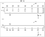
- A) is a top view which shows the structure of the static elimination apparatus as a modification of the said static elimination apparatus
- (b) is a top view which shows the structure of the static elimination apparatus which concerns on Embodiment 1.
- FIG. It is a top view which shows the structure of the static elimination apparatus as a further modification of the said static elimination apparatus.
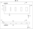
- the structure of the static elimination apparatus as a further modification of the said static elimination apparatus is shown, (a) is a top view of a static elimination apparatus, (b) is a side view of a static elimination apparatus.
- the structure of the static elimination apparatus as a further modification of the said static elimination apparatus is shown, (a) is a top view of a static elimination apparatus, (b) is a side view of a static elimination apparatus.
- the structure of the static elimination apparatus as a further modification of the said static elimination apparatus is shown, (a) is a top view of a static elimination apparatus, (b) is a side view of a static elimination apparatus.
- the structure of the static elimination apparatus as a further modification of the said static elimination apparatus is shown, and it is a top view of a static elimination apparatus.
- (A) And (b) is a figure explaining the effect in the said static elimination apparatus. It is a figure which shows an image forming apparatus provided with a light-shielding member.
- FIG. 1 It is a top view which shows the light-guide plate as a modification of the light-guide plate F with which the said static elimination apparatus is provided.
- the structure of the static elimination apparatus as a further modification of the said static elimination apparatus is shown, (a) is a top view of a static elimination apparatus, (b) is a side view of a static elimination apparatus.
- the structure of the static elimination apparatus as a further modification of the said static elimination apparatus is shown, (a) is a top view of a static elimination apparatus, (b) is a side view of a static elimination apparatus.
- the structure of the static elimination apparatus as a further modification of the said static elimination apparatus is shown, (a) is a top view of a static elimination apparatus, (b) is a side view of a static elimination apparatus.
- the structure of the static elimination apparatus as a further modification of the said static elimination apparatus is shown, and it is a top view of a static elimination apparatus. It is a figure explaining the effect in the said static elimination apparatus.
- the structure of the static elimination apparatus as a further modification of the said static elimination apparatus is shown, (a) is a top view of a static elimination apparatus, (b) is a side view of a static elimination apparatus.
- the structure of the static elimination apparatus as a further modification of the said static elimination apparatus is shown, (a) is a top view of a static elimination apparatus, (b) is a side view of a static elimination apparatus.
- the structure of the static elimination apparatus as a further modification of the said static elimination apparatus is shown, (a) is a top view of a static elimination apparatus, (b) is a side view of a static elimination apparatus.
- Embodiment 1 an embodiment according to an aspect of the present invention (hereinafter, also referred to as “this embodiment”) will be described with reference to the drawings.
- this embodiment described below is only an illustration of the present invention in all respects. It goes without saying that various improvements and modifications can be made without departing from the scope of the present invention. That is, in implementing the present invention, a specific configuration according to the embodiment may be adopted as appropriate.
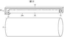
- FIG. 2 is a perspective view showing the configuration of the static elimination device 10.
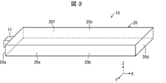
- FIG. 3 is a perspective view showing the configuration of the light guide plate 20.
- the X-axis direction shown in FIG. 3 may be referred to as a length direction
- the Y-axis direction as a width direction
- the Z-axis direction as a height direction.
- FIG. 4 is a plan view of the light guide plate 20.
- the static eliminator 10 includes a light source 11, a light guide plate 20, an optical sensor 12, and a housing 13, and irradiates light to the photosensitive drum 2 included in the image forming apparatus 1.
- the light guide plate 20 is a member that guides light incident from the light source 11 and irradiates the guided light toward the photosensitive drum 2.
- the light guide plate 20 has a rectangular parallelepiped shape, and includes a light incident surface 20a, a light reflecting surface 20b (first surface), a light emitting surface 20c (second surface), and a light incident surface. It has a facing surface 20d that faces 20a, a side surface 20e, and a side surface 20f.
- the light incident surface 20 a is a surface on which the light source 11 is installed, and is a surface on which light is incident from the light source 11 into the light guide plate 20.
- the light reflecting surface 20b is a surface perpendicular to the light incident surface 20a, and an optical path changing unit 21 (reflective structure unit) that reflects light incident from the light incident surface 20a toward the light emitting surface 20c is formed.
- the light emitting surface 20 c is a surface parallel to the light reflecting surface 20 b and emits the light reflected by the optical path changing unit 21 toward the photosensitive drum 2.
- the number of optical path changing portions 21 formed on the light reflecting surface 20b increases as the distance from the light incident surface 20a increases.
- variations in the amount of light emitted from the light exit surface 20c can be suppressed in the length direction of the light guide plate 20 (in other words, the direction in which light is guided through the light guide plate 20). In other words, in the length direction of the light guide plate 20, the amount of light emitted from the light emitting surface 20c can be made uniform.
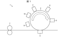
- FIG. 1 is an enlarged view of the image forming apparatus 1 around the photosensitive drum 2 included in the image forming apparatus 1.
- the image forming apparatus 1 forms (prints) an image by an electrophotographic method, and is, for example, a copying machine, a printer, a facsimile, or a complex machine thereof.
- members other than those shown below may be interpreted as being the same as known members.
- an image forming apparatus 1 includes a photosensitive drum 2, which is a photosensitive member that functions as an image carrier, a charger 3, an exposure device 4, a developing device 5, a transfer device 6, and a fixing device. A device 7, a cleaning device 8, and a static elimination device 10 are provided.
- the printing operation on the recording paper in the image forming apparatus 1 will be described.
- the surface of the photosensitive drum 2 is uniformly charged by the charger 3.
- the photosensitive drum 2 has a drum shape, and rotates in the direction of the arrow shown inside the photosensitive drum 2 in FIG.
- the surface of the photosensitive drum 2 is exposed to laser light by the exposure device 4. Thereby, an electrostatic latent image based on the image data is formed on the surface of the photosensitive drum 2.
- the developing device 5 attaches a toner agent to the surface of the photosensitive drum 2 and develops a toner image (developed image) based on the above-described electrostatic latent image on the surface of the photosensitive drum 2.
- the transfer device 6 transfers the toner image developed on the surface of the photosensitive drum 2 onto a recording sheet.
- the fixing device 7 heats and pressurizes the recording paper, thereby melting the toner image transferred to the recording paper and fixing the toner image on the recording paper. Thereby, an image is printed on the recording paper.
- the toner agent remaining on the surface of the photosensitive drum 2 after the transfer is removed by the cleaning device 8. Then, the charge (residual charge) remaining on the surface of the photosensitive drum 2 is removed by irradiating the surface of the photosensitive drum 2 with light by the static eliminator 10. As a result, the photosensitive drum 2 is ready for printing on the next recording sheet.
- the static eliminator 10 includes a light source 11, a light guide plate 20, an optical sensor 12, and a housing 13.
- the light source 11 irradiates the light guide plate 20 with light.
- the light source 11 is, for example, an LED (Light Emitting diode) light source.
- the light source 11 is disposed adjacent to the light incident surface 20a at the center in the width direction of the light guide plate 20 described later.
- the photosensitive drum 2 has a wavelength that is easily discharged depending on the design. Therefore, it is preferable that the light source 11 emits light in a narrow wavelength region including light having a wavelength suitable for neutralizing the photosensitive drum 2.
- the light guide plate 20 is a member that guides light incident from the light source 11 and irradiates the guided light toward the photosensitive drum 2.
- the light guide plate 20 is formed of a resin material that is transparent and has a relatively high refractive index.
- a material for forming the light guide plate 20 for example, polycarbonate resin, polymethyl methacrylate resin, cycloolefin polymer resin, or the like can be used.
- the light guide plate 20 is formed of a polymethyl methacrylate resin.
- the light guide plate 20 has a rectangular parallelepiped shape, and includes a light incident surface 20a, a light reflecting surface 20b, a light emitting surface 20c, a facing surface 20d facing the light incident surface 20a, and a side surface. 20e and a side surface 20f.
- the light incident surface 20 a is a surface on which the light source 11 is installed, and is a surface on which light is incident from the light source 11 into the light guide plate 20.
- the light reflecting surface 20b is a surface perpendicular to the light incident surface 20a, and an optical path changing unit 21 (details will be described later) that reflects the light incident from the light incident surface 20a toward the light emitting surface 20c. Is formed.
- the light emitting surface 20 c is a surface parallel to the light reflecting surface 20 b and emits the light reflected by the optical path changing unit 21 toward the photosensitive drum 2.
- the distance between the light reflecting surface 20b and the light emitting surface 20c is preferably, for example, not more than half the diameter of the photosensitive drum 2.
- the static eliminator 10 is installed such that the light emitting surface 20c of the light guide plate 20 faces the photosensitive drum 2, and the length direction of the light emitting surface 20c is the width direction of the photosensitive drum 2 (FIG. 2). reference).
- the optical sensor 12 is a sensor that is installed on the opposing surface 20d of the light guide plate 20 and measures the amount of light that has reached the opposing surface 20d.
- the housing 13 stores each part of the static eliminator 10 inside.
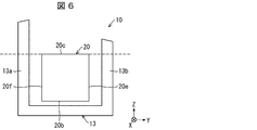
- the housing 13 has a rectangular parallelepiped shape, and only the surface corresponding to the light emitting surface 20c of the light guide plate 20 is an opening (see FIG. 6).
- FIG. 4 is a plan view of the light guide plate 20. As shown in FIG. 4, a large number of optical path changing portions 21 are formed on the light reflection surface 20 b of the light guide plate 20.
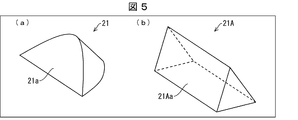
- FIG. 5A is a perspective view showing the shape of the optical path changing unit 21 in the present embodiment
- FIG. 5B shows the shape of an optical path changing unit 21A as a modification of the optical path changing unit 21.
- FIG. It is a perspective view.
- the optical path change part 21 is comprised by the circular-arc-shaped cone, and is provided with the reflective surface 21a which is a plane.
- the optical path changing unit 21 is formed so that the side where the reflecting surface 21a and the light reflecting surface 20b are in contact is the width direction (that is, the Y-axis direction). Thereby, the light incident from the light incident surface 20a is reflected by the reflecting surface 21a toward the light emitting surface 20c (in other words, reflected toward the + Z-axis direction).
- the optical path changing portion formed on the light reflecting surface 20b is not limited to the shape shown in FIG. 5A, and may be any shape as long as it has a flat reflecting surface. .
- the optical path changing portion formed on the light reflecting surface 20b may have a triangular prism shape including the reflecting surface 21Aa.
- the both ends of the optical path changing part are not flat by making the optical path changing part into the shape shown in FIG. 5A, sagging occurs when the optical path changing part is formed by injection molding. There is an advantage that the moldability is high.
- the amount of light emitted from the light source and reaching the optical path changing unit varies depending on the distance from the light incident surface. That is, light having a large amount of light reaches the optical path changing unit that is close to the light incident surface, while light having a small amount of light reaches the optical path changing unit that is far from the light incident surface. Therefore, when the light path changing part is formed on the light reflecting surface with a constant density regardless of the distance from the light incident surface as in the conventional static elimination device, the amount of light emitted from the light emitting surface is light incident. It depends on the distance from the surface. For this reason, there is a problem in that unevenness occurs in the amount of light applied to the photosensitive drum 2 and unevenness occurs in the degree of charge removal of the photosensitive drum 2.
- the number of optical path changing portions 21 formed on the light reflecting surface 20b increases as the distance from the light incident surface 20a increases. (In other words, the density of the optical path changing unit 21 is high).
- the area that reflects the light per unit area is small, while the light with a small amount of light from the light source 11 arrives.
- the area for reflecting light per unit area is large.
- the distance between the light reflection surface 20b and the light-projection surface 20c, ie, the light-guide plate 20, is demonstrated.
- the thickness can be reduced.
- the light guide plate 20 can be reduced in size.
- the static eliminator 10 can be downsized.
- the reflection surface 21a of the optical path changing unit 21 is a flat surface.
- the range of light emitted from the static eliminator 10 can be stored in a linear or rectangular shape. As a result, it is possible to concentrate light in a necessary region, so that the charge removal speed on the surface of the photosensitive drum 2 can be improved. Thereby, the printing speed can be improved.
- the printing process by the leakage light to other than static elimination area Adverse effects on the toner (for example, a decrease in the adhesion of the toner agent) can be prevented.
- the angle formed between the light reflecting surface 20b of the light guide plate 20 and the reflecting surface 21a of the optical path changing unit 21 is preferably 35 ° to 55 °. Thereby, the advancing direction of the light reflected by the reflective surface 21a can be made into the angle near perpendicular
- FIG. 6 is a diagram illustrating the structure of the housing 13.
- the housing 13 includes a side surface 13 a that faces the side surface 20 e of the light guide plate 20 and a side surface 13 b that faces the side surface 20 f of the light guide plate 20.
- the housing 13 is formed of a white resin and can reflect light.
- the housing 13 is arranged so that the side surface 13a is on the side where the photosensitive drum 2 rotates relative to the side surface 13b (in other words, the side on which the charger 3 is installed).
- the side surface 13 a and the side surface 13 b are formed so that the end portion on the photosensitive drum 2 side is higher than the light emitting surface 20 c of the light guide plate 20.
- the height of the side surface 13a on the charger 3 side is higher than the height of the side surface 13b. This makes it difficult for unexpected light to be applied to the charger 3 side.
- the housing 13 may be made of a black resin. Therefore, since the light which is not irradiated to a desired direction can be absorbed by the side surface 13a and the side surface 13b, it can prevent that the light irradiated from the static elimination apparatus 10 is irradiated to the unexpected part.
- FIG. 7 is a block diagram showing a configuration of a main part of the static eliminator 10.
- the static eliminator 10 includes a control unit 14.
- the control unit 14 acquires information on the amount of light measured by the optical sensor 12 and sets the intensity of light irradiated on the light source 11 based on the information. Thereby, it can adjust so that the light quantity of the light irradiated from the static elimination apparatus 10 may turn into a suitable light quantity.
- the optical path changing unit 21 is formed inside the light guide plate 20 on the light reflecting surface 20b. That is, the optical path changing unit 21 is formed to have a convex shape inside the light reflecting surface 20b, but is not limited thereto. That is, the optical path changing unit 21 may be formed on the light reflecting surface 20b so as to have a convex shape from the light reflecting surface 20b toward the outside of the light guide plate 20.
- the light source 11 is an LED light source as described above.
- the light source 11 may be, for example, an LED light source including a light emitting element and a lens that parallelizes the direction of light emitted from the light emitting element in a predetermined direction. Thereby, the light irradiated from the light source 11 can be irradiated only in a predetermined direction.
- the light source 11 may be a general LED light source including a light emitting element and a resin that seals the light emitting element. According to this configuration, the light source 11 can be easily mounted.
- the reflection surface 21a of the optical path changing unit 21 has a constant angle with the light reflection surface 20b regardless of the distance from the light incident surface 20a.
- the reflecting surface 21a of the optical path changing unit 21 may be formed such that the angle formed with the light reflecting surface 20b increases as the distance from the light incident surface 20a increases.
- FIG. 8A is a plan view showing the configuration of the static eliminator 10A in the present modification
- FIG. 8B is a plan view showing the configuration of the static eliminator 10 in the first embodiment.
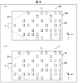
- FIG. 8B a region near the light incident surface 20a (in other words, the light source 11) and near the end of the light guide plate 20 in the width direction (Y-axis direction) (FIG. 8).
- the optical path changing unit 21 formed in a region between the dotted line and the light incident surface 20a shown in FIG.
- the angle formed between the light irradiated to the region and the reflecting surface 21a in the plane parallel to the XY plane is smaller than the light irradiated to the other region.
- the light is reflected by the optical path changing unit 21 formed in the region between the dotted line and the light incident surface 20a shown in FIG. There is a possibility that the light will be irradiated to an unexpected part.
- the static eliminator 10A in the present modification includes a light guide plate 20A instead of the light guide plate 20 in the first embodiment, as shown in FIG.
- the optical path changing unit 21 is not formed in the region between the dotted line shown in FIG. 8 and the light incident surface 20a. Thereby, it can prevent that an irradiation angle spreads with the light radiate
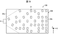
- FIG. 9 is a plan view showing a configuration of a static eliminator 10B in the present modification.
- the static eliminator 10B includes a light guide plate 20B instead of the light guide plate 20 in the first embodiment.
- the reflection surface 21a of the optical path changing unit 21 formed on the light reflection surface 20b faces the direction of the light source 11 in a plane parallel to the XY plane (that is, a plane parallel to the light reflection surface 20b). Is formed. However, it is not necessary that the reflecting surface 21a of the optical path changing unit 21 is strictly oriented in the direction of the light source 11, and there may be some deviation.
- the reflecting surface 21a of the optical path changing unit 21 is directed to the center side in the width direction of the light guide plate 20 rather than the direction parallel to the light incident surface 20a. Therefore, the traveling direction of the light reflected by the light incident surface 20 a can be set to the center side in the width direction of the light guide plate 20. Thereby, the spread of the irradiation angle of the light emitted from the light emitting surface 20c can be suppressed. That is, it is possible to suppress the light emitted from the static eliminator 10 from being emitted in an unexpected direction.
- FIGS. 10A and 10B show the configuration of the static eliminator 10C according to this modification.
- FIG. 10A is a top view of the static eliminator 10C
- FIG. 10B is a side view of the static eliminator 10C.
- the static eliminator 10 ⁇ / b> C includes a light guide plate 20 ⁇ / b> C instead of the light guide plate 20 in the first embodiment.
- the light guide plate 20 ⁇ / b> C includes a plurality of optical path changing units 22.
- the optical path changing unit 22 is formed to extend in the width direction (Y-axis direction) of the light guide plate 20 and is formed over the entire width direction of the light guide plate 20C.
- the heights of the plurality of optical path changing units 22 are the same.
- the number of the optical path changing units 22 per unit area increases as the distance from the light incident surface 20a increases.
- the number of the optical path changing units 22 per unit area is small, so the region that reflects light is small.
- the number of the optical path changing units 22 per unit area is large, and thus the region that reflects light is large.
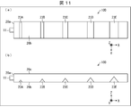
- FIG. 11 shows a configuration of a static eliminator 10D according to this modification.
- FIG. 11A is a top view of the static eliminator 10D
- FIG. 11B is a side view of the static eliminator 10D.
- the static eliminator 10D includes a light guide plate 20D instead of the light guide plate 20 in the first embodiment.
- the light guide plate 20D includes optical path changing units 23A to 23E as optical path changing units.
- the optical path changing portions 23A to 23E are formed to extend in the width direction (Y-axis direction) of the light guide plate 20, and are formed over the entire width direction of the light guide plate 20.
- the height of the optical path changing unit increases. That is, the height of the optical path changing unit 23A is lower, and the height increases in the order of the optical path changing unit 23B, the optical path changing unit 23C, the optical path changing unit 23D, and the optical path changing unit 23E.
- an optical path change part for example, optical path change part 23A
- attains the area
- the height of the optical path changing unit for example, the optical path changing unit 23E
- the region that reflects light is large.
- the amount of light emitted from the light exit surface 20c can be suppressed in the length direction of the light guide plate 20D (in other words, the direction in which light is guided through the light guide plate 20D). In other words, the amount of light emitted from the light emitting surface 20c can be made uniform in the length direction of the light guide plate 20D.
- the light guide plate 20D has been described with a configuration including five optical path changing units (optical path changing units 23A to 23E).
- the number of optical path changing units is not particularly limited, and may be changed as appropriate. May be.
- FIG. 12 shows a configuration of a static eliminator 10E according to this modification.
- FIG. 12A is a top view of the static eliminator 10E
- FIG. 12B is a side view of the static eliminator 10E.
- the static eliminator 10E includes a light guide plate 20E instead of the light guide plate 20 in the first embodiment.
- the light guide plate 20E includes optical path changing units 24A to 24G as optical path changing units.
- the optical path changing units 24A to 24G are formed to extend in the width direction (Y-axis direction) of the light guide plate 20E.
- the optical path changing units 24A to 24G have the same height.
- the length in the direction parallel to the light incident surface (Y-axis direction) of the optical path changing unit becomes longer.
- the length in the Y-axis direction of the optical path changing unit 24A is the shortest, and the Y axis in the order of the optical path changing unit 24B, the optical path changing unit 24C, the optical path changing unit 24D, the optical path changing unit 24E, the optical path changing unit 24F, and the optical path changing unit 24G.
- the length of the direction is longer.
- the length in the Y-axis direction of the optical path changing unit (for example, the optical path changing unit 24A) is short in the region close to the light incident surface 20a where the light having a large amount of light from the light source 11 reaches, The reflective area is small.
- the length of the optical path changing unit (optical path changing unit 24G) in the Y-axis direction is long. large.
- variation in the amount of light emitted from the light exit surface 20c can be suppressed in the length direction of the light guide plate 20E (in other words, the direction in which light is guided through the light guide plate 20E).
- the amount of light emitted from the light exit surface 20c can be made uniform in the length direction of the light guide plate 20E.
- the light guide plate 20E has been described as having a configuration including seven optical path changing units (optical path changing units 24A to 24G).
- the number of optical path changing units is not particularly limited, and may be changed as appropriate. May be.
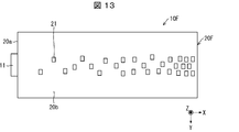
- FIG. 13 is a top view of the static eliminator 10F, showing the configuration of the static eliminator 10F in the present modification. As illustrated in FIG. 13, the static eliminator 10F includes a light guide plate 20F instead of the light guide plate 20 in the first embodiment.
- the light guide plate 20 ⁇ / b> F includes a plurality of optical path changing units 21.
- the number of the optical path changing units 21 formed on the light reflecting surface 20b increases (in other words, the density of the optical path changing unit 21 increases.
- the optical path changing portion 21 is formed only in the central portion in the width direction of the light guide plate 20F.
- FIG. 14A and 14B are diagrams for explaining the effect of the static eliminator 10F.
- FIG. 14A is a diagram illustrating the light irradiation range in the static eliminator 10.
- FIG. 14B is a diagram illustrating the light irradiation range in the static eliminator 10F. is there.
- the optical path changing portion 21 is formed in a predetermined region in the width direction of the light guide plate 20F (in the present modification, only the central portion). Yes. Thereby, the range in which light is radiate
- the optical path changing unit 21 is formed only at the central portion in the width direction of the light guide plate 20F, the amount of light reflected by one optical path changing unit 21 is increased. As a result, it is possible to increase the amount of light (that is, the illuminance) applied to the region where light is to be irradiated.
- the width of the light guide plate 20F since the optical path changing unit 21 is formed only in the center portion in the width direction of the light guide plate 20F, it is not necessary to reduce the width of the light guide plate 20F. As a result, it is possible to irradiate light to a region to be irradiated without impairing moldability.
- a light blocking member that blocks part of the light emitted from the light guide plate may be provided between the static eliminator and the photosensitive drum. This will be described with reference to FIG.
- FIG. 15 shows an image forming apparatus provided with a light shielding member
- (a) is a diagram showing a case where the static eliminator 10 according to Embodiment 1 is used
- the light guide plate 30 is provided in a region other than the region where light is to be irradiated on the photosensitive drum 2 by providing the light shielding member 30. It can suppress that the light radiate
- the static eliminator 10F in the present modification when the static eliminator 10F in the present modification is used, by providing the light shielding member 30, the light exit surface 20c of the light emitted from the light guide plate 20F is provided.
- the light blocking member 30 since light that is not vertical can be blocked by the light blocking member 30, it is possible to irradiate only the region of the photosensitive drum 2 where light is to be irradiated.
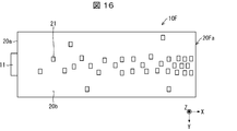
- FIG. 16 is a top view showing a light guide plate 20Fa as a modified example of the light guide plate 20F of the present modified example.
- most of the optical path changing portion 21 is formed in a predetermined region in the width direction of the light guide plate 20Fa (in the present modification, only the central portion). In other regions, other optical path changing portions are formed in the central portion. Even in this configuration, it is possible to irradiate most of the light emitted from the light guide plate 20Fa on the region of the photosensitive drum 2 where the light is desired to be irradiated.
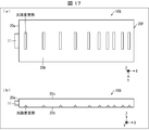
- FIG. 17 shows a configuration of a static eliminator 10G as a modified example of the static eliminator 10C in the modified example 3, (a) is a top view of the static eliminator 10G, and (b) is a diagram of the static eliminator 10G. It is a side view.
- FIG. 18 shows a configuration of a static eliminator 10H as a modified example of the static eliminator 10D in the modified example 4, (a) is a top view of the static eliminator 10H, and (b) is a diagram of the static eliminator 10H. It is a side view.
- FIG. 18 shows a configuration of a static eliminator 10H as a modified example of the static eliminator 10D in the modified example 4
- (a) is a top view of the static eliminator 10H
- (b) is a diagram of the static eliminator 10H. It is a side view.
- FIG. 18 shows a configuration of a static eliminator 10H as a modified example of the static eliminator 10D in the modified example 4
- FIG. 19 shows a configuration of a static eliminator 10I as a modified example of the static eliminator 10E in the modified example 5, (a) is a top view of the static eliminator 10I, and (b) is a diagram of the static eliminator 10I. It is a side view.
- the optical path changing portions are formed only at the center portions in the width direction of the respective light guide plates 20F, 20G, and 20H.
- FIG. 20 shows the configuration of the static eliminator 10J in the present modification, and is a top view of the static eliminator 10J.
- the static eliminator 10J includes a light guide plate 20I instead of the light guide plate 20 in the first embodiment.
- the light guide plate 20I includes a plurality of optical path changing units 21.
- the number of optical path changing units 21 formed on the light reflecting surface 20b increases (in other words, the density of the optical path changing unit 21 increases).
- the optical path changing portion 21 is formed only on one side in the width direction of the light guide plate 20F.
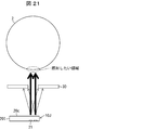
- FIG. 21 is a diagram for explaining the effect of the static eliminator 10J.
- the static eliminator 10F according to the modified example 7 when used, there is a case where light cannot be irradiated to an area to be irradiated on the photosensitive drum 2.
- the optical path changing unit 21 is formed only on one side in the width direction of the light guide plate 20I. As a result, the light emitted from the light guide plate 20I can be applied to the region of the photosensitive drum 2 to be irradiated.
- FIG. 22 shows a configuration of a static eliminator 10K as a modified example of the static eliminator 10C in the modified example 3, (a) is a top view of the static eliminator 10K, and (b) is a diagram of the static eliminator 10K. It is a side view.
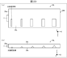
- FIG. 23 shows a configuration of a static eliminator 10L as a modified example of the static eliminator 10D in the modified example 4, (a) is a top view of the static eliminator 10L, and (b) is a diagram of the static eliminator 10L. It is a side view.
- FIG. 22 shows a configuration of a static eliminator 10K as a modified example of the static eliminator 10C in the modified example 3
- (a) is a top view of the static eliminator 10K
- (b) is a diagram of the static eliminator 10K. It is a side view.
- FIG. 23 shows a configuration of a static eliminator 10L as a modified example of the static eliminator 10D in the modified example 4
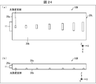
- FIG. 24 shows a configuration of a static eliminator 10M as a modified example of the static eliminator 10E in the modified example 5, (a) is a top view of the static eliminator 10M, and (b) is a diagram of the static eliminator 10M. It is a side view.
- the optical path changing portions are formed only on one side in the width direction of the respective light guide plates 20J, 20K, and 20L.
- the light emitted from the light guide plates 20F, 20G, and 20H can be irradiated onto the region of the photosensitive drum 2 that is desired to be irradiated.
- the static eliminator is a static eliminator including a light source and a light guide plate that guides light incident from the light source and emits the guided light
- the light guide plate includes: A light incident surface on which light from the light source is incident, and a first surface that is perpendicular to the light incident surface and includes a plurality of reflecting structures that reflect the light incident from the light incident surface by a reflecting surface; A second surface that is parallel to the first surface and emits light reflected by the reflective structure, and according to a distance from the light incident surface, per unit area on the first surface
- the areas of the reflecting surfaces are different.
- the amount of light emitted from the second surface of the light guide plate is made more uniform. Can do.
- the distance between the first surface and the second surface that is, the thickness of the light guide plate can be reduced.
- the area of the reflecting surface per unit area in a region close to the light incident surface is equal to the reflection per unit area in another region.
- the configuration may be smaller than the area of the surface.
- the density of the reflecting surface that reflects light is small in the region close to the light incident surface where the light with a large amount of light from the light source reaches, while the light incident surface with which the light with a small amount of light from the light source reaches In the region far from the surface, the density of the reflecting surface that reflects light is large.
- variations in the amount of light emitted from the light exit surface can be suppressed in the direction in which light is guided through the light guide plate.
- the amount of light emitted from the second surface can be made uniform in the length direction of the light guide plate.
- the density of the reflective structure unit per unit area in a region near the light incident surface is per unit area in the other region.
- the configuration may be smaller than the density of the reflection structure portion.
- the area of the reflecting surface per unit area in the region close to the light incident surface in the direction in which light is guided is changed by changing the density of the reflecting structure portion. It can be made smaller than the area of the hit reflective surface.
- the plurality of reflective structure units are configured such that the reflective surface is formed in a direction parallel to the light incident surface, and the light guide plate has a whole direction parallel to the light incident surface. Per unit area in a region close to the light incident surface in a direction in which the light is guided in the direction in which the light is guided.
- the number of the reflective structure portions may be smaller than the number of the reflective structure portions per unit area in the other region.
- the area of the reflective surface can be made smaller than the area of the reflective surface per unit area in other regions.
- the plurality of reflective structure units include the reflective surface formed in a direction parallel to the light incident surface, and the light guide plate over the entire direction parallel to the reflective surface.
- the reflection surface per unit area in a region close to the light incident surface in the direction in which the light is guided by changing the height of the reflection structure in the direction in which the light is guided. Can be made smaller than the area of the reflecting surface per unit area in other regions.
- the plurality of reflective structure units have the reflective surface formed in a direction parallel to the light incident surface, and the height of the reflective surface from the first surface. Are the same, and in the direction in which the light is guided, the length of the reflective structure portion in the region near the light incident surface in the direction parallel to the light incident surface is the reflective structure portion in the other region.
- the structure which is shorter than the length of the direction parallel to the said light-incidence surface may be sufficient.
- the area of the reflecting surface per unit area in the region close to the light incident surface can be made smaller than the area of the reflecting surface per unit area in the other regions.
- the reflecting surfaces of the plurality of reflecting structures are in a plane parallel to the first surface, more than a direction parallel to the light incident surface with respect to the light incident surface.
- the structure may be formed facing the light source.
- the traveling direction of the light reflected by the light incident surface can be set to the center side in the width direction of the light guide plate. Therefore, the spread of the irradiation angle of the light emitted from the light emitting surface can be suppressed. That is, it is possible to suppress the light emitted from the static eliminator from being emitted in an unexpected direction.
- the light guide plate in the first surface in a direction near the light incident surface and in a direction perpendicular to a direction in which the light of the light guide plate is guided in a direction near the light incident surface and in a direction perpendicular to a direction in which the light of the light guide plate is guided.
- a configuration in which the reflective structure portion is not formed in a region near the end portion may be employed.
- the region is irradiated.
- the angle between the reflecting surface and the reflecting surface in the plane parallel to the light reflecting surface is smaller than the light irradiated to other regions. Therefore, the irradiation angle of the light reflected from the reflection structure and emitted from the second surface is widened, and the light irradiated from the static eliminator may be irradiated to an unexpected part.
- the reflecting structure portion is not formed in the region near the light incident surface and in the vicinity of the end portion in the width direction of the light guide plate, the irradiation angle is widened. Can be prevented.
- the static eliminator further includes a housing that stores the light guide plate and the light source, and the housing has an opening corresponding to the second surface.
- the first surface and the second surface are provided with side surfaces that face each other, and at least one of the side surfaces has an end on the opening side that is closer to the second surface than the second surface.
- emitted may be sufficient.
- the light that is not irradiated in a desired direction when emitted from the second surface can be reflected by the side surface. Therefore, it can prevent that the light irradiated from a static elimination apparatus is irradiated to the unexpected part.
- the static eliminator neutralizes residual charges existing on the surface of the photosensitive drum included in the image forming apparatus, and the light is guided in the light guide plate. And the opening side end of the side surface on the side where the charger for charging the photosensitive drum is installed in the image forming apparatus.
- the configuration may be such that the light is emitted from the second surface in a direction that is emitted from the second surface.
- An image forming apparatus includes any one of the static eliminators described above.
Landscapes
- Health & Medical Sciences (AREA)
- Toxicology (AREA)
- Physics & Mathematics (AREA)
- General Physics & Mathematics (AREA)
- Discharging, Photosensitive Material Shape In Electrophotography (AREA)
- Electrophotography Configuration And Component (AREA)
Abstract
導光板の光出射面から出射される光の光量をより均一化することができ、かつ、導光板の厚みが小さい除電装置を実現する。除電装置(10)は、光源(11)と、導光板(20)とを備える。導光板(20)は、光源(11)から光が入射される光入射面(20a)と、光入射面(20a)から入射された光を反射面によって反射する複数の光路変更部(21)を備える光反射面(20b)と、光反射面(20b)に平行であり、光路変更部(21)によって反射された光を出射する光出射面と、を備え、光入射面(20a)からの距離に応じて、光反射面(20b)における短面積当たりの反射面の面積が異なっている。
Description
本発明は、光を照射することにより感光体の除電を行う除電装置、および除電装置を備える画像形成装置に関する。
電子写真方式の画像形成装置では、以下のような過程で画像形成(印刷)が行われる。まず、像担持体として作用する感光体(例えば、感光体ドラム)の表面を静電気によって帯電し、帯電された領域に対してレーザー光により画像露光して静電潜像を形成する。次に、感光体上に形成した静電潜像をトナー像として現像し、現像されたトナー像を中間転写ベルトなどの中間転写体や記録紙などの記録材に静電的に転写する。
電子写真方式の画像形成装置では、感光体の表面を帯電する前に感光体の表面上の電荷を除去するための除電装置を備えている。このような除電装置が、例えば特許文献1に開示されている。
特許文献1に開示された除電装置では、光源からの光を入射する光入射面と、光入射面から入射した光を出射する光出射面とを有しており、光入射面及び光出射面以外の外周面に、光反射部材が設けられている。上記の構成により、感光体に照射される光の光量を大きくさせている。
しかしながら、特許文献1の技術では、光を光出射面に向けて反射させるための凹凸部が光出射面の反対側面に形成されている。当該凹凸部は、導光板の厚み方向に沿って延びており、各凹凸部が同じ大きさであり、かつ、入射面に対して垂直な方向に沿って等間隔で形成されている。そのため、入射面に近い領域から出射される光の光量と、光出射面から遠い領域から出射される光の光量とが大きく異なってしまうという問題を有している。
また、特許文献1には、光出射面から照射される光の光量を均一化させるために、光出射面と反対側面との距離を、光入射面から遠ざかるにしたがって小さくする技術が開示されている。しかしながら、当該構成を実現するためには、導光板の光出射面と反対側面との間に厚みを大きくする必要があり、除電装置が大型化してしまうという問題があった。
本発明の一態様は、導光板の光出射面から出射される光の光量をより均一化することができ、かつ、導光板の厚みが小さい除電装置を実現することを目的とする。
上記の課題を解決するために、本発明の一態様に係る除電装置は、光源と、前記光源から入射された光を導光し、導光した光を出射する導光板と、を備える除電装置であって、前記導光板は、前記光源から光が入射される光入射面と、前記光入射面に対して垂直であり、前記光入射面から入射された光を反射面によって反射する複数の反射構造部を備える第1面と、前記第1面に平行であり、前記反射構造部によって反射された光を出射する第2面と、を備え、前記光入射面からの距離に応じて、前記第1面における単位面積当たりの前記反射面の面積が異なっている。
本発明の一態様によれば、カーボンナノチューブの成長温度までカーボンナノチューブ成長用基板を加熱する際に、高い昇温速度で加熱しても中間層にクラックが発生しないカーボンナノチューブ成長用基板を実現するという効果を奏する。
〔実施形態1〕
以下、本発明の一側面に係る実施の形態(以下、「本実施形態」とも表記する)を、図面に基づいて説明する。ただし、以下で説明する本実施形態は、あらゆる点において本発明の例示に過ぎない。本発明の範囲を逸脱することなく種々の改良や変形を行うことができることは言うまでもない。つまり、本発明の実施にあたって、実施形態に応じた具体的構成が適宜採用されてもよい。
以下、本発明の一側面に係る実施の形態(以下、「本実施形態」とも表記する)を、図面に基づいて説明する。ただし、以下で説明する本実施形態は、あらゆる点において本発明の例示に過ぎない。本発明の範囲を逸脱することなく種々の改良や変形を行うことができることは言うまでもない。つまり、本発明の実施にあたって、実施形態に応じた具体的構成が適宜採用されてもよい。
§1 適用例
まず、図2~図4を用いて、本発明が適用される場面の一例について説明する。図2は、除電装置10の構成を示す斜視図である。図3は、導光板20の構成を示す斜視図である。以降の説明では、図3に示すX軸方向を長さ方向、Y軸方向を幅方向、Z軸方向を高さ方向と称して説明する場合がある。図4は、導光板20の平面図である。
まず、図2~図4を用いて、本発明が適用される場面の一例について説明する。図2は、除電装置10の構成を示す斜視図である。図3は、導光板20の構成を示す斜視図である。以降の説明では、図3に示すX軸方向を長さ方向、Y軸方向を幅方向、Z軸方向を高さ方向と称して説明する場合がある。図4は、導光板20の平面図である。
図2に示すように、除電装置10は、光源11と、導光板20と、光センサ12と、筐体13とを備えており、画像形成装置1が備える感光体ドラム2に光を照射する。導光板20は、光源11から入射された光を導光し、導光した光を感光体ドラム2へ向けて照射する部材である。
図3に示すように、導光板20は、直方体形状をしており、光入射面20aと、光反射面20b(第1面)と、光出射面20c(第2面)と、光入射面20aと対向する対向面20dと、側面20eと、側面20fとを備えている。
光入射面20aは、光源11が設置される面であり、光源11から導光板20の内部に光が入射される面である。光反射面20bは、光入射面20aに対して垂直な面であり、光入射面20aから入射された光を光出射面20cへ向けて反射する光路変更部21(反射構造部)が形成されている。光出射面20cは、光反射面20bと平行な面であり、光路変更部21によって反射された光を感光体ドラム2へ向けて出射する。
本実施形態における除電装置10では、図4に示すように、光入射面20aからの距離が大きくなるにつれて光反射面20bに形成される光路変更部21の数が多くなっている。
上記の構成によれば、光源11からの光量が大きい光が到達する光入射面20aに近い領域では光を反射する領域が小さい一方で、光源11からの光量が小さい光が到達する光入射面20aから遠い領域では光を反射する領域が大きい。その結果、導光板20の長さ方向(換言すれば、導光板20の内部を光が導光される方向)において、光出射面20cから出射される光の光量のバラツキを抑えることができる。換言すれば、導光板20の長さ方向において、光出射面20cから出射される光の光量を均一化することができる。
§2 構成例
以下、除電装置10および除電装置10を備える画像形成装置1の構成例を、図面を参照して説明する。図1は、画像形成装置1が備える感光体ドラム2の周辺における画像形成装置1の拡大図である。画像形成装置1は、電子写真方式によって画像を形成(印刷)するものであり、例えば、複写機、プリンタ、ファクシミリ、およびそれらの複合機などである。なお、画像形成装置1について、以下に示す部材以外の部材については、公知の部材と同様であると解釈されてよい。
以下、除電装置10および除電装置10を備える画像形成装置1の構成例を、図面を参照して説明する。図1は、画像形成装置1が備える感光体ドラム2の周辺における画像形成装置1の拡大図である。画像形成装置1は、電子写真方式によって画像を形成(印刷)するものであり、例えば、複写機、プリンタ、ファクシミリ、およびそれらの複合機などである。なお、画像形成装置1について、以下に示す部材以外の部材については、公知の部材と同様であると解釈されてよい。
図1に示すように、画像形成装置1は、像担持体として機能する感光体である感光体ドラム2と、帯電器3と、露光装置4と、現像装置5と、転写装置6と、定着装置7と、クリーニング装置8と、除電装置10と、を備えている。
ここで、画像形成装置1における記録紙への印刷の動作について説明する。画像形成装置1における印刷動作では、まず、帯電器3により感光体ドラム2の表面を一様に帯電させる。なお、感光体ドラム2は、ドラム形状をしており、図1において感光体ドラム2の内部に示す矢印方向に回転する。
次に、露光装置4により感光体ドラム2の表面にレーザー光を露光させる。これにより、画像データに基づく静電潜像が感光体ドラム2の表面に形成される。次に、現像装置5が、トナー剤を感光体ドラム2の表面に付着させ、上述の静電潜像に基づくトナー像(顕像)を感光体ドラム2の表面に現像する。次に、転写装置6が、感光体ドラム2の表面に現像されたトナー像を記録紙に転写する。次に、定着装置7が、記録紙を加熱および加圧することにより、記録紙に転写されたトナー像を融解させ、記録紙にトナー像を定着させる。これにより、記録紙に画像が印刷される。
転写後の感光体ドラム2の表面に残留するトナー剤は、クリーニング装置8によって除去される。そして、除電装置10によって感光体ドラム2の表面に光を照射することにより、感光体ドラム2の表面に残留する電荷(残留電荷)を除去する。これにより、感光体ドラム2が次の記録紙への印刷が可能な状態となる。
(除電装置10)
次に、本実施形態における除電装置10について図面を参照しながら詳細に説明する。図2に示すように、除電装置10は、光源11と、導光板20と、光センサ12と、筐体13とを備えている。
次に、本実施形態における除電装置10について図面を参照しながら詳細に説明する。図2に示すように、除電装置10は、光源11と、導光板20と、光センサ12と、筐体13とを備えている。
光源11は、導光板20に光を照射する。光源11は、例えばLED(Light Emitting
diode)光源である。光源11は、後述する導光板20の幅方向の中央において、光入射面20aに隣接して設置されている。なお、感光体ドラム2は、その設計に応じて除電されやすい波長が存在する。そのため、光源11は、感光体ドラム2の除電に好適な波長の光を含む狭い波長領域の光を照射することが好ましい。
diode)光源である。光源11は、後述する導光板20の幅方向の中央において、光入射面20aに隣接して設置されている。なお、感光体ドラム2は、その設計に応じて除電されやすい波長が存在する。そのため、光源11は、感光体ドラム2の除電に好適な波長の光を含む狭い波長領域の光を照射することが好ましい。
導光板20は、光源11から入射された光を導光し、導光した光を感光体ドラム2へ向けて照射する部材である。導光板20は、透明で屈折率が比較的高い樹脂材料で成形される。導光板20を形成する材料としては、例えばポリカーボネイト樹脂、ポリメチルメタクリレート樹脂、シクロオレフィンポリマー樹脂などを使用することができる。本実施形態では、導光板20は、ポリメチルメタクリレート樹脂によって成形されている。
図3に示すように、導光板20は、直方体形状をしており、光入射面20aと、光反射面20bと、光出射面20cと、光入射面20aと対向する対向面20dと、側面20eと、側面20fとを備えている。
光入射面20aは、光源11が設置される面であり、光源11から導光板20の内部に光が入射される面である。
光反射面20bは、光入射面20aに対して垂直な面であり、光入射面20aから入射された光を光出射面20cへ向けて反射する光路変更部21(詳しくは、後述する)が形成されている。
光出射面20cは、光反射面20bと平行な面であり、光路変更部21によって反射さされた光を感光体ドラム2へ向けて出射する。
光反射面20bと光出射面20cとの間の距離は、例えば、感光体ドラム2の直径の半分以下とすることが好ましい。
除電装置10は、導光板20の光出射面20cが感光体ドラム2に対向し、かつ、光出射面20cの長さ方向が感光体ドラム2の幅方向となるように設置される(図2参照)。
光センサ12は、導光板20の対向面20dに設置されており、対向面20dに到達した光の光量を測定するセンサである。
筐体13は、除電装置10の各部を内部に格納する。筐体13は、直方体形状をしており、導光板20の光出射面20cに対応する面のみが開口となっている(図6参照)。
次に、導光板20の光反射面20bに形成されている光路変更部21の形状および配置について、図4および図5を参照しながら詳細に説明する。
図4は、導光板20の平面図である。図4に示すように、導光板20に光反射面20bには、多数の光路変更部21が形成されている。
図5の(a)は、本実施形態における光路変更部21の形状を示す斜視図であり、図5の(b)は、光路変更部21の変形例としての光路変更部21Aの形状を示す斜視図である。図5の(a)に示すように、光路変更部21は、円弧状の錐にて構成されており、平面である反射面21aを備えている。本実施形態では、反射面21aと、光反射面20bとが接する辺が幅方向(すなわち、Y軸方向)となるように、光路変更部21が形成されている。これにより、光入射面20aから入射した光は、反射面21aによって光出射面20cに向かって反射される(換言すれば、+Z軸方向に向けて反射される)。
なお、光反射面20bに形成される光路変更部は、図5の(a)に示す形状に限られるものではなく、平面の反射面を有する形状であればどのような形状であってもよい。例えば、図5の(b)に示すように、光反射面20bに形成される光路変更部は、反射面21Aaを備える三角柱形状であってもよい。なお、光路変更部を図5の(a)に示す形状にすることにより、光路変更部の両端部が平面となっていないので、光路変更部を射出成型して形成する際にダレが発生せず成形性が高いという利点がある。
ここで、光源から出射され光路変更部に達する光の光量は、光入射面からの距離に応じて異なる。すなわち、光入射面からの距離が近い光路変更部には光量が大きい光が到達する一方で、光入射面からの距離が遠い光路変更部には光量が小さい光が到達する。そのため、従来の除電装置のように、光入射面からの距離に関わらず一定の密度で光路変更部が光反射面に形成されている場合、光出射面から出射される光の光量が光入射面からの距離によって異なってしまう。そのため、感光体ドラム2に照射する光の光量にムラが生じてしまい、感光体ドラム2の除電の程度にムラができてしまうという問題があった。
これに対して、本実施形態における除電装置10では、図4に示すように、光入射面20aからの距離が大きくなるにつれて光反射面20bに形成される光路変更部21の数が多くなっている(換言すれば、光路変更部21の密度が高くなっている)。
上記の構成によれば、光源11からの光量が大きい光が到達する光入射面20aに近い領域では単位面積当たりの光を反射する面積が小さい一方で、光源11からの光量が小さい光が到達する光入射面20aから遠い領域では単位面積当たりの光を反射する面積が大きい。その結果、導光板20の長さ方向(換言すれば、導光板20の内部を光が導光される方向)において、光出射面20cから出射される光の光量のバラツキを抑えることができる。換言すれば、導光板20の長さ方向において、光出射面20cから出射される光の光量を均一化することができる。
また、上記の構成によれば、特許文献1の技術のように、光反射面を傾斜させる必要がないため、光反射面20bと光出射面20cとの間の距離、すなわち、導光板20の厚みを小さくすることができる。その結果、導光板20を小型化することができる。引いては、除電装置10を小型化することができる。
また、上述したように、光路変更部21の反射面21aは平面になっている。除電装置10から照射される光の範囲を線状または長方形状に収めることができる。その結果、必要な領域に光を集中させることができるので、感光体ドラム2の表面の除電速度を向上させることができる。これにより、印刷速度を向上させることができる。また、反射面21aが曲面にてなっている場合に比べて除電装置10から照射される光が予期しない箇所に照射されることを防ぐことができるので、除電エリア以外への漏れ光による印刷プロセスへの悪影響(例えば、トナー剤の付着力低下)を防ぐことができる。
また、導光板20の光反射面20bと、光路変更部21の反射面21aとのなす角度は、35°~55°であることが好ましい。これにより、反射面21aによって反射された光の進行方向を光出射面20cに対して垂直に近い角度とすることができる。その結果、除電装置10から照射される光が予期しない箇所に照射されることを防ぐことができる。
次に、筐体13の構造について図6を参照しながら説明する。図6は、筐体13の構造を示す図である。図6に示すように、筐体13は、導光板20の側面20eと対向する側面13aと、導光板20の側面20fと対向する側面13bとを備えている。筐体13は、白色の樹脂にて形成されており、光を反射できるようになっている。
筐体13は、側面13aが側面13bに対して感光体ドラム2が回転する側(換言すれば、帯電器3が設置されている側)となるように配置されている。図6に示すように、側面13aおよび側面13bは、感光体ドラム2側の端部が、導光板20の光出射面20cよりも高くなるように形成されている。これにより、光出射面20cから出射されたときに、所望の方向に照射されない光を側面13aおよび側面13bによって反射することができる。これにより、除電装置10から照射される光が予期しない箇所に照射されることを防ぐことができる。
特に、帯電器3側に予期しない光が照射されてしまうと、感光体ドラム2を帯電器3によって帯電する際に悪影響を及ぼしてしまう。そのため、図6に示すように、帯電器3側となる側面13aの高さが、側面13bの高さよりも高くなっている。これにより、帯電器3側に予期しない光が照射されにくくなっている。
なお、本発明の一態様の除電装置10では、筐体13は黒色の樹脂にて構成されてもよい。これにより、所望の方向に照射されない光を側面13aおよび側面13bによって吸収することができるので、除電装置10から照射される光が予期しない箇所に照射されることを防ぐことができる。
図7は、除電装置10の要部の構成を示すブロック図である。図7に示すように、除電装置10は、制御部14を備えている。制御部14は、光センサ12が測定した光の光量の情報を取得し、当該情報に基づいて、光源11に対して照射する光の強さを設定する。これにより、除電装置10から照射される光の光量が適切な光量となるように調整することができる。
本実施形態では、光路変更部21は、光反射面20bにおいて導光板20の内部に形成されていた。すなわち、光路変更部21は、光反射面20bの内部に凸形状となるように形成されていたがこれに限られない。すなわち、光路変更部21は、光反射面20bから導光板20の外部へ向けて凸形状となるように光反射面20bに形成されてもよい。
光源11は、上述したようにLED光源である。光源11は、例えば、発光素子と、当該発光素子から照射された光の方向を所定の方向に平行化させるレンズとを含むLED光源であってもよい。これにより、光源11から照射される光を所定の方向のみに照射することができる。また、光源11は、発光素子と、当該発光素子を封止する樹脂とを備える、一般的なLED光源であってもよい。当該構成によれば、光源11を実装させやすくなる。
なお、本実施形態では、光路変更部21の反射面21aは、光入射面20aからの距離に関わらず、光反射面20bとのなす角度が一定であったが、本発明の除電装置はこれに限られない。例えば、光路変更部21の反射面21aは、光入射面20aからの距離が大きくなるにつれて、光反射面20bとのなす角度が大きくなるように形成されてもよい。
§3 変形例
以上、本開示の実施の形態を詳細に説明してきたが、前述までの説明はあらゆる点において本開示の例示に過ぎない。本開示の範囲を逸脱することなく種々の改良や変形を行うことができることは言うまでもない。例えば、以下のような変更が可能である。なお、以下では、上記実施形態と同様の構成要素に関しては同様の符号を用い、上記実施形態と同様の点については、適宜説明を省略した。以下の変形例は適宜組み合わせ可能である。
以上、本開示の実施の形態を詳細に説明してきたが、前述までの説明はあらゆる点において本開示の例示に過ぎない。本開示の範囲を逸脱することなく種々の改良や変形を行うことができることは言うまでもない。例えば、以下のような変更が可能である。なお、以下では、上記実施形態と同様の構成要素に関しては同様の符号を用い、上記実施形態と同様の点については、適宜説明を省略した。以下の変形例は適宜組み合わせ可能である。
<変形例1>
図8の(a)は、本変形例における除電装置10Aの構成を示す平面図であり、(b)は、実施形態1における除電装置10の構成を示す平面図である。
図8の(a)は、本変形例における除電装置10Aの構成を示す平面図であり、(b)は、実施形態1における除電装置10の構成を示す平面図である。
まず、図8の(b)に示すように、光入射面20a(換言すれば、光源11)に近く、かつ、導光板20の幅方向(Y軸方向)の端部付近の領域(図8に示す点線と光入射面20aとの間の領域)に形成された光路変更部21に、光入射面20aから入射された光が照射された場合について説明する。この場合、当該領域に照射される光は、他の領域に照射される光に比べて、XY平面と平行な面における反射面21aとのなす角度が小さくなってしまう。そのため、図8に示す点線と光入射面20aとの間の領域に形成された光路変更部21によって反射され、光出射面20cから出射する光によって照射角度が広がってしまい、除電装置10から照射される光が予期しない箇所に照射されてしまう可能性がある。
これに対して、本変形例における除電装置10Aは、図8の(a)に示すように、実施形態1における導光板20に代えて導光板20Aを備えている。導光板20Aでは、図8に示す点線と光入射面20aとの間の領域に光路変更部21が形成されていない。これにより、光出射面20cから出射する光によって照射角度が広がってしまうことを防ぐことができるようになっている。
<変形例2>
図9は、本変形例における除電装置10Bの構成を示す平面図である。図9に示すように、除電装置10Bは、実施形態1における導光板20に代えて導光板20Bを備えている。
図9は、本変形例における除電装置10Bの構成を示す平面図である。図9に示すように、除電装置10Bは、実施形態1における導光板20に代えて導光板20Bを備えている。
導光板20Bでは、光反射面20bに形成される光路変更部21の反射面21aが、XY平面と平行な面(すなわち、光反射面20bと平行な平面)において、光源11の方向を向くように形成されている。ただし、光路変更部21の反射面21aが厳密に光源11の方向を向くように形成されている必要はなく、多少のずれがあってもよい。
上記の構成によれば、光路変更部21の反射面21aが光入射面20aに対して平行な方向よりも、導光板20の幅方向の中央側に向いた状態となる。そのため、光入射面20aによって反射された光の進行方向を導光板20の幅方向の中央側にすることができる。これにより、光出射面20cから出射される光の照射角度の広がりを抑制することができる。すなわち、除電装置10から照射される光が予期しない方向へ出射されることを抑制することができる。
<変形例3>
図10は、本変形例における除電装置10Cの構成を示すものであり、(a)は、除電装置10Cの上面図であり、(b)は、除電装置10Cの側面図である。図10の(a)および(b)に示すように、除電装置10Cは、実施形態1における導光板20に代えて導光板20Cを備えている。
図10は、本変形例における除電装置10Cの構成を示すものであり、(a)は、除電装置10Cの上面図であり、(b)は、除電装置10Cの側面図である。図10の(a)および(b)に示すように、除電装置10Cは、実施形態1における導光板20に代えて導光板20Cを備えている。
導光板20Cは、複数の光路変更部22を備えている。光路変更部22は、導光板20の幅方向(Y軸方向)に延びて形成されており、導光板20Cの幅方向全体にわたって形成されている。複数の光路変更部22の高さは、同一となっている。導光板20Cでは、光入射面20aからの距離が大きくなるにつれて単位面積当たりの光路変更部22の数が多くなっている。
上記の構成によれば、光源11からの光量が大きい光が到達する光入射面20aに近い領域では、単位面積当たりの光路変更部22の数が少ないため、光を反射する領域が小さい。その一方で、光源11からの光量が小さい光が到達する光入射面20aから遠い領域では、単位面積当たりの光路変更部22の数が多いため、光を反射する領域が大きい。その結果、導光板20Cの長さ方向(換言すれば、導光板20Cの内部を光が導光される方向)において、光出射面20cから出射される光の光量のバラツキを抑えることができる。換言すれば、導光板20の長さ方向において、光出射面20cから出射される光の光量を均一化することができる。
<変形例4>
図11は、本変形例における除電装置10Dの構成を示すものであり、(a)は、除電装置10Dの上面図であり、(b)は、除電装置10Dの側面図である。図11の(a)および(b)に示すように、除電装置10Dは、実施形態1における導光板20に代えて導光板20Dを備えている。
図11は、本変形例における除電装置10Dの構成を示すものであり、(a)は、除電装置10Dの上面図であり、(b)は、除電装置10Dの側面図である。図11の(a)および(b)に示すように、除電装置10Dは、実施形態1における導光板20に代えて導光板20Dを備えている。
導光板20Dは、光路変更部として光路変更部23A~23Eを備えている。光路変更部23A~23Eは、導光板20の光反射面20bと、光路変更部23A~23Eの反射面とのなす角度が同一となっている。光路変更部23A~23Eは、導光板20の幅方向(Y軸方向)に延びて形成されており、導光板20の幅方向全体にわたって形成されている。導光板20Dでは、光入射面20aからの距離が大きくなるにつれて、光路変更部の高さが高くなっている。すなわち、光路変更部23Aの高さがもっと低く、光路変更部23B、光路変更部23C、光路変更部23D、光路変更部23Eの順に高さが高くなっている。
上記の構成によれば、光源11からの光量が大きい光が到達する光入射面20aに近い領域では光路変更部(例えば、光路変更部23A)の高さが低いため、光を反射する領域が小さい。その一方で、光源11からの光量が小さい光が到達する光入射面20aから遠い領域では、光路変更部(例えば、光路変更部23E)の高さが高いため、光を反射する領域が大きい。その結果、導光板20Dの長さ方向(換言すれば、導光板20Dの内部を光が導光される方向)において、光出射面20cから出射される光の光量のバラツキを抑えることができる。換言すれば、導光板20Dの長さ方向において、光出射面20cから出射される光の光量を均一化することができる。
なお、上記の説明では、導光板20Dは、5つの光路変更部(光路変更部23A~23E)を備える構成について説明したが、光路変更部の数は、特に限定されるものではなく、適宜変更してもよい。
<変形例5>
図12は、本変形例における除電装置10Eの構成を示すものであり、(a)は、除電装置10Eの上面図であり、(b)は、除電装置10Eの側面図である。図12の(a)および(b)に示すように、除電装置10Eは、実施形態1における導光板20に代えて導光板20Eを備えている。
図12は、本変形例における除電装置10Eの構成を示すものであり、(a)は、除電装置10Eの上面図であり、(b)は、除電装置10Eの側面図である。図12の(a)および(b)に示すように、除電装置10Eは、実施形態1における導光板20に代えて導光板20Eを備えている。
導光板20Eは、光路変更部として光路変更部24A~24Gを備えている。光路変更部24A~24Gは、導光板20の光反射面20bと、光路変更部23A~23Eの反射面とのなす角度が同一となっている。光路変更部24A~24Gは、導光板20Eの幅方向(Y軸方向)に延びて形成されている。光路変更部24A~24Gの高さは、同一となっている。導光板20Dでは、光入射面20aからの距離が大きくなるにつれて、光路変更部の光入射面と平行な方向(Y軸方向)の長さが長くなっている。すなわち、光路変更部24AのY軸方向の長さが最も短く、光路変更部24B、光路変更部24C、光路変更部24D、光路変更部24E、光路変更部24F、光路変更部24Gの順にY軸方向の長さが長くなっている。
上記の構成によれば、光源11からの光量が大きい光が到達する光入射面20aに近い領域では光路変更部(例えば、光路変更部24A)のY軸方向の長さが短いため、光を反射する領域が小さい。その一方で、光源11からの光量が小さい光が到達する光入射面20aから遠い領域では、光路変更部(光路変更部24G)のY軸方向の長さが長いため、光を反射する領域が大きい。その結果、導光板20Eの長さ方向(換言すれば、導光板20Eの内部を光が導光される方向)において、光出射面20cから出射される光の光量のバラツキを抑えることができる。換言すれば、導光板20Eの長さ方向において、光出射面20cから出射される光の光量を均一化することができる。
なお、上記の説明では、導光板20Eは、7つの光路変更部(光路変更部24A~24G)を備える構成について説明したが、光路変更部の数は、特に限定されるものではなく、適宜変更してもよい。
<変形例6>
図13は、本変形例における除電装置10Fの構成を示すものであり、除電装置10Fの上面図である。除電装置10Fは、図13に示すように、実施形態1における導光板20に代えて導光板20Fを備えている。
図13は、本変形例における除電装置10Fの構成を示すものであり、除電装置10Fの上面図である。除電装置10Fは、図13に示すように、実施形態1における導光板20に代えて導光板20Fを備えている。
導光板20Fは、複数の光路変更部21を備えている。導光板20Fでは、光入射面20aからの距離が大きくなるにつれて光反射面20bに形成される光路変更部21の数が多くなっている(換言すれば、光路変更部21の密度が高くなっている)とともに、光路変更部21が導光板20Fの幅方向における中央部のみに形成されている。
図14は、除電装置10Fにおける効果を説明するものであり、(a)は除電装置10における光の照射範囲を示す図であり、(b)は除電装置10Fにおける光の照射範囲を示す図である。
図14の(a)に示すように、除電装置10では、光路変更部21が導光板20の幅方向全体にわたって形成されているため、導光板20の幅方向全体から光が出射する。そのため、光を照射したい領域以外に対しても感光体ドラム2に導光板20から出射した光が照射されてしまう。その結果、感光体ドラム2に対して意図しない領域に導電性を与えてしまう可能性がある。
これに対して、除電装置10Fでは、図14の(b)に示すように、光路変更部21が導光板20Fの幅方向における所定の領域(本変形例では、中央部のみ)に形成されている。これにより、導光板20Fから光が出射される範囲を狭くすることができる。その結果、感光体ドラム2における光を照射したい領域に導光板20Fから出射した光の大部分を照射することができる。
また、除電装置10Fでは、光路変更部21が導光板20Fの幅方向における中央部のみに形成されていることにより、1つの光路変更部21によって反射する光の量が多くなる。その結果、光を照射したい領域に照射する光量(すなわち、照度)を多くすることができる。
なお、導光板の幅を小さくすることにより、導光板から光が出射される範囲を狭くすることが考えられる。しかしながら、導光板の幅を小さくすると、導光板の成形性が悪くなってしまい、導光板の製造が困難になってしまう。これに対して、導光板20Fでは、光路変更部21を導光板20Fの幅方向における中央部のみに形成するため、導光板20Fの幅を小さくする必要がない。その結果、成形性を損なわずに照射したい領域に光を照射することができる。
また、本発明の一態様の画像形成装置では、除電装置と感光体ドラムとの間に、導光板から出射された光の一部を遮光する遮光部材を備えていてもよい。これについて、図15を参照しながら説明する。
図15は、遮光部材を備える画像形成装置を示すものであり、(a)は、実施形態1における除電装置10を用いた場合を示す図であり、(b)は、本変形例における除電装置10Fを用いた場合を示す図である。
図15の(a)に示すように、実施形態1における除電装置10を用いた場合には、遮光部材30を設けることにより、感光体ドラム2における光を照射したい領域以外の領域に、導光板20から出射した光が照射されることを抑制することができる。
また、図15の(b)に示すように、本変形例における除電装置10Fを用いた場合には、遮光部材30を設けることにより、導光板20Fから出射された光のうち光出射面20c対して垂直ではない光を遮光部材30によって遮光することができるため、感光体ドラム2における光を照射したい領域にのみ光を照射することができる。
図16は、本変形例の導光板20Fの変形例としての導光板20Faを示す上面図である。本発明の一態様の除電装置では、図16に示すように、導光板20Faの幅方向における所定の領域(本変形例では、中央部のみ)に光路変更部21の大部分が形成されており、その他の領域に中央部にその他の光路変更部が形成されている。当該構成においても、感光体ドラム2における光を照射したい領域に導光板20Faから出射した光の大部分を照射することができる。
図17は、変形例3における除電装置10Cの変形例としての除電装置10Gの構成を示すものであり、(a)は、除電装置10Gの上面図であり、(b)は、除電装置10Gの側面図である。図18は、変形例4における除電装置10Dの変形例としての除電装置10Hの構成を示すものであり、(a)は、除電装置10Hの上面図であり、(b)は、除電装置10Hの側面図である。図19は、変形例5における除電装置10Eの変形例としての除電装置10Iの構成を示すものであり、(a)は、除電装置10Iの上面図であり、(b)は、除電装置10Iの側面図である。
図17~図19に示すように、除電装置10G・10H・10Iにおいても、それぞれの導光板20F・20G・20Hの幅方向の中央部のみに光路変更部が形成されている。これにより、導光板20Fから光が出射される範囲を狭くすることができるので、感光体ドラム2における光を照射したい領域に導光板から出射した光の大部分を照射することができる。
<変形例7>
図20は、本変形例における除電装置10Jの構成を示すものであり、除電装置10Jの上面図である。除電装置10Jは、図20に示すように、実施形態1における導光板20に代えて導光板20Iを備えている。
図20は、本変形例における除電装置10Jの構成を示すものであり、除電装置10Jの上面図である。除電装置10Jは、図20に示すように、実施形態1における導光板20に代えて導光板20Iを備えている。
導光板20Iは、複数の光路変更部21を備えている。導光板20Iでは、光入射面20aからの距離が大きくなるにつれて光反射面20bに形成される光路変更部21の数が多くなっている(換言すれば、光路変更部21の密度が高くなっている)とともに、光路変更部21が導光板20Fの幅方向における一方側のみに形成されている。
図21は、除電装置10Jにおける効果を説明する図である。ここで、画像形成装置の配置の制約により、変形例7における除電装置10Fを用いた場合、感光体ドラム2における照射したい領域に対して光を照射できない場合がある。それに対して、除電装置10Jでは、図21に示すように、光路変更部21が導光板20Iの幅方向における一方側のみに形成されている。これにより、導光板20Iからの出射された光を感光体ドラム2における照射したい領域に照射することができる。
図22は、変形例3における除電装置10Cの変形例としての除電装置10Kの構成を示すものであり、(a)は、除電装置10Kの上面図であり、(b)は、除電装置10Kの側面図である。図23は、変形例4における除電装置10Dの変形例としての除電装置10Lの構成を示すものであり、(a)は、除電装置10Lの上面図であり、(b)は、除電装置10Lの側面図である。図24は、変形例5における除電装置10Eの変形例としての除電装置10Mの構成を示すものであり、(a)は、除電装置10Mの上面図であり、(b)は、除電装置10Mの側面図である。
図22~図24に示すように、除電装置10K・10L・10Mにおいても、それぞれの導光板20J・20K・20Lの幅方向の一方側のみに光路変更部が形成されている。これにより、導光板20F・20G・20Hからの出射された光を感光体ドラム2における照射したい領域に照射することができる。
〔まとめ〕
本発明の一態様に係る除電装置は、光源と、前記光源から入射された光を導光し、導光した光を出射する導光板と、を備える除電装置であって、前記導光板は、前記光源から光が入射される光入射面と、前記光入射面に対して垂直であり、前記光入射面から入射された光を反射面によって反射する複数の反射構造部を備える第1面と、前記第1面に平行であり、前記反射構造部によって反射された光を出射する第2面と、を備え、前記光入射面からの距離に応じて、前記第1面における単位面積当たりの前記反射面の面積が異なっている。
本発明の一態様に係る除電装置は、光源と、前記光源から入射された光を導光し、導光した光を出射する導光板と、を備える除電装置であって、前記導光板は、前記光源から光が入射される光入射面と、前記光入射面に対して垂直であり、前記光入射面から入射された光を反射面によって反射する複数の反射構造部を備える第1面と、前記第1面に平行であり、前記反射構造部によって反射された光を出射する第2面と、を備え、前記光入射面からの距離に応じて、前記第1面における単位面積当たりの前記反射面の面積が異なっている。
上記構成によれば、光入射面からの距離に応じて、第1面における反射面の面積を異ならせているため、導光板の第2面から出射される光の光量をより均一化させることができる。また、第1面を傾斜させる必要がないため、第1面と第2面との間の距離、すなわち、導光板の厚みを小さくすることができる。
本開示の一態様に係る除電装置において、前記光が導光される方向において、前記光入射面に近い領域における単位面積当たりの前記反射面の面積が、他の領域における単位面積当たりの前記反射面の面積よりも小さくなっている構成であってもよい。
上記の構成によれば、光源からの光量が大きい光が到達する光入射面に近い領域では光を反射する反射面の密度が小さい一方で、光源からの光量が小さい光が到達する光入射面から遠い領域では光を反射する反射面の密度が大きい。その結果、導光板の内部を光が導光される方向において、光出射面から出射される光の光量のバラツキを抑えることができる。換言すれば、導光板の長さ方向において、第2面から出射される光の光量を均一化することができる。
本開示の一態様に係る除電装置において、前記光が導光される方向において、前記光入射面に近い領域における単位面積当たりの前記反射構造部の密度が、前記他の領域における単位面積当たりの前記反射構造部の密度よりも小さくなっている構成であってもよい。
上記の構成によれば、反射構造部の密度を変化させることにより、光が導光される方向において、光入射面に近い領域における単位面積当たりの反射面の面積を、他の領域における単位面積当たりの反射面の面積よりも小さくすることができる。
本開示の一態様に係る除電装置において、前記複数の反射構造部は、前記反射面が前記光入射面と平行な方向に形成されており、前記導光板において前記光入射面と平行な方向全体にわたって形成されており、前記反射面が前記第1面からの高さが同一となるように形成されており、前記光が導光される方向において、前記光入射面に近い領域における単位面積当たりの前記反射構造部の数が、前記他の領域における単位面積当たりの前記反射構造部の数よりも少なくなっている構成であってもよい。
上記の構成によれば、光が導光される方向において、単位面積当たりの反射構造部の数を変化させることにより、光が導光される方向において、光入射面に近い領域における単位面積当たりの反射面の面積を、他の領域における単位面積当たりの反射面の面積よりも小さくすることができる。
本開示の一態様に係る除電装置において、前記複数の反射構造部は、前記反射面が前記光入射面と平行な方向に形成されており、前記導光板において前記反射面と平行な方向全体にわたって形成されており、前記光が導光される方向において、前記光入射面に近い領域における前記反射構造部の高さが、前記他の領域における前記反射構造部の高さよりも低くなっている構成であってもよい。
上記の構成によれば、光が導光される方向において、反射構造部の高さを変化させることにより、光が導光される方向において、光入射面に近い領域における単位面積当たりの反射面の面積を、他の領域における単位面積当たりの反射面の面積よりも小さくすることができる。
本開示の一態様に係る除電装置において、前記複数の反射構造部は、前記反射面が前記光入射面と平行な方向に形成されており、前記反射面の、前記第1面からの高さが同一であり、前記光が導光される方向において、前記光入射面に近い領域における前記反射構造部の前記光入射面と平行な方向の長さが、前記他の領域における前記反射構造部の前記光入射面と平行な方向の長さよりも短くなっている構成であってもよい。
上記の構成によれば、光が導光される方向において、導光板の中央における反射構造部の光入射面と平行な方向の長さを変化させることにより、光が導光される方向において、光入射面に近い領域における単位面積当たりの反射面の面積を、他の領域における単位面積当たりの反射面の面積よりも小さくすることができる。
本開示の一態様に係る除電装置において、前記複数の反射構造部の前記反射面は、前記第1面と平行な平面において、前記光入射面に対して前記光入射面に平行な方向よりも、前記光源に向いて形成されている構成であってもよい。
上記の構成によれば、光入射面によって反射された光の進行方向を導光板の幅方向の中央側にすることができる。これにより、光出射面から出射される光の照射角度の広がりを抑制することができる。すなわち、除電装置から照射される光が予期しない方向へ出射されることを抑制することができる。
本開示の一態様に係る除電装置において、前記第1面における、前記光入射面に近い領域であり、かつ、前記導光板の前記光が導光される方向と垂直な方向における前記導光板の端部付近の領域に、前記反射構造部が形成されていない構成であってもよい。
ここで、光入射面に近く、かつ、導光板の幅方向の端部付近の領域に形成された反射構造部に、光入射面から入射された光が照射された場合、当該領域に照射される光は、他の領域に照射される光に比べて、光反射面に平行な面における反射面とのなす角度が小さくなってしまう。そのため、反射構造部によって反射され、第2面から出射する光の照射角度が広がってしまい、除電装置から照射される光が予期しない箇所に照射されてしまう可能性がある。
これに対して、上記の構成によれば、光入射面に近く、かつ、導光板の幅方向の端部付近の領域に反射構造部が形成されていないので、照射角度が広がってしまうことを防ぐことができる。
本開示の一態様に係る除電装置において、前記導光板および前記光源を格納する筐体をさらに備え、前記筐体は、前記第2面に対応する面が開口となっており、前記導光板の前記第1面と前記第2面とを接続する面とそれぞれ対向する側面を備えており、前記側面の少なくとも一方は、前記開口側の端部が、前記第2面よりも前記第2面から光が出射される方向に延びている構成であってもよい。
上記構成によれば、第2面から出射されたときに、所望の方向に照射されない光を側面によって反射することができる。これにより、除電装置から照射される光が予期しない箇所に照射されることを防ぐことができる。
本開示の一態様に係る除電装置において、前記除電装置は、画像形成装置が備える感光体ドラムの表面に存在する残留電荷を除電するものであり、前記導光板の前記光が導光される方向に平行な方向が感光体ドラムの幅方向となるように設置され、前記画像形成装置において前記感光体ドラムを帯電するための帯電器が設置される側の前記側面の前記開口側の端部が、前記第2面よりも前記第2面から光が出射される方向に延びている構成であってもよい。
上記の構成によれば、帯電器側に予期しない光が照射されることを抑制することができる。
本開示の一態様に係る画像形成装置は、上記のいずれかの除電装置を備える。
本発明は上述した各実施形態に限定されるものではなく、請求項に示した範囲で種々の変更が可能であり、異なる実施形態にそれぞれ開示された技術的手段を適宜組み合わせて得られる実施形態についても本発明の技術的範囲に含まれる。
1 画像形成装置
2 感光体ドラム
3 帯電器
10、10A~10M 除電装置
11 光源
13 筐体
13a、13b 側面
20、20A~20L 導光板
20a 光入射面
20b 光反射面(第1面)
20c 光出射面(第2面)
21、21A、22、23A~23E、24A~24G 光路変更部(反射構造部)
21a、21Aa 反射面
2 感光体ドラム
3 帯電器
10、10A~10M 除電装置
11 光源
13 筐体
13a、13b 側面
20、20A~20L 導光板
20a 光入射面
20b 光反射面(第1面)
20c 光出射面(第2面)
21、21A、22、23A~23E、24A~24G 光路変更部(反射構造部)
21a、21Aa 反射面
Claims (11)
- 光源と、前記光源から入射された光を導光し、導光した光を出射する導光板と、を備える除電装置であって、
前記導光板は、
前記光源から光が入射される光入射面と、
前記光入射面に対して垂直であり、前記光入射面から入射された光を反射面によって反射する複数の反射構造部を備える第1面と、
前記第1面に平行であり、前記反射構造部によって反射された光を出射する第2面と、を備え、
前記光入射面からの距離に応じて、前記第1面における単位面積当たりの前記反射面の面積が異なっていることを特徴とする除電装置。 - 前記光が導光される方向において、前記光入射面に近い領域における単位面積当たりの前記反射面の面積が、他の領域における単位面積当たりの前記反射面の面積よりも小さくなっていることを特徴とする請求項1に記載の除電装置。
- 前記光が導光される方向において、前記光入射面に近い領域における単位面積当たりの前記反射構造部の密度が、前記他の領域における単位面積当たりの前記反射構造部の密度よりも小さくなっていることを特徴とする請求項2に記載の除電装置。
- 前記複数の反射構造部は、
前記反射面が前記光入射面と平行な方向に形成されており、
前記導光板において前記光入射面と平行な方向全体にわたって形成されており、
前記反射面が前記第1面からの高さが同一となるように形成されており、
前記光が導光される方向において、前記光入射面に近い領域における単位面積当たりの前記反射構造部の数が、前記他の領域における単位面積当たりの前記反射構造部の数よりも少なくなっていることを特徴とする請求項2に記載の除電装置。 - 前記複数の反射構造部は、
前記反射面が前記光入射面と平行な方向に形成されており、
前記導光板において前記反射面と平行な方向全体にわたって形成されており、
前記光が導光される方向において、前記光入射面に近い領域における前記反射構造部の高さが、前記他の領域における前記反射構造部の高さよりも低くなっていることを特徴とする請求項2に記載の除電装置。 - 前記複数の反射構造部は、
前記反射面が前記光入射面と平行な方向に形成されており、
前記反射面の、前記第1面からの高さが同一であり、
前記光が導光される方向において、前記光入射面に近い領域における前記反射構造部の前記光入射面と平行な方向の長さが、前記他の領域における前記反射構造部の前記光入射面と平行な方向の長さよりも短くなっていることを特徴とする請求項2に記載の除電装置。 - 前記複数の反射構造部の前記反射面は、前記第1面と平行な平面において、前記光入射面に対して前記光入射面に平行な方向よりも、前記光源に向いて形成されていることを特徴とする請求項1~3のいずれか1項に記載の除電装置。
- 前記第1面における、前記光入射面に近い領域であり、かつ、前記導光板の前記光が導光される方向と垂直な方向における前記導光板の端部付近の領域に、前記反射構造部が形成されていないことを特徴とする請求項2に記載の除電装置。
- 前記導光板および前記光源を格納する筐体をさらに備え、
前記筐体は、
前記第2面に対応する面が開口となっており、
前記導光板の前記第1面と前記第2面とを接続する面とそれぞれ対向する側面を備えており、
前記側面の少なくとも一方は、前記開口側の端部が、前記第2面よりも前記第2面から光が出射される方向に延びていることを特徴とする請求項1~8のいずれか1項に記載の除電装置。 - 前記除電装置は、
画像形成装置が備える感光体ドラムの表面に存在する残留電荷を除電するものであり、
前記導光板の前記光が導光される方向に平行な方向が感光体ドラムの幅方向となるように設置され、
前記画像形成装置において前記感光体ドラムを帯電するための帯電器が設置される側の前記側面の前記開口側の端部が、前記第2面よりも前記第2面から光が出射される方向に延びていることを特徴とする請求項9に記載の除電装置。 - 請求項1~10のいずれか1項に記載の除電装置を備えた画像形成装置。
Priority Applications (2)
| Application Number | Priority Date | Filing Date | Title |
|---|---|---|---|
| DE112018007098.0T DE112018007098T5 (de) | 2018-02-15 | 2018-12-05 | Statischer eliminator und bilderzeugnisvorrichtung |
| JP2020500291A JP7060076B2 (ja) | 2018-02-15 | 2018-12-05 | 除電装置および画像形成装置 |
Applications Claiming Priority (2)
| Application Number | Priority Date | Filing Date | Title |
|---|---|---|---|
| JP2018025114 | 2018-02-15 | ||
| JP2018-025114 | 2018-02-15 |
Publications (1)
| Publication Number | Publication Date |
|---|---|
| WO2019159503A1 true WO2019159503A1 (ja) | 2019-08-22 |
Family
ID=67619843
Family Applications (1)
| Application Number | Title | Priority Date | Filing Date |
|---|---|---|---|
| PCT/JP2018/044708 Ceased WO2019159503A1 (ja) | 2018-02-15 | 2018-12-05 | 除電装置および画像形成装置 |
Country Status (3)
| Country | Link |
|---|---|
| JP (1) | JP7060076B2 (ja) |
| DE (1) | DE112018007098T5 (ja) |
| WO (1) | WO2019159503A1 (ja) |
Cited By (1)
| Publication number | Priority date | Publication date | Assignee | Title |
|---|---|---|---|---|
| JP2022175412A (ja) * | 2021-05-13 | 2022-11-25 | 京セラドキュメントソリューションズ株式会社 | 画像形成装置 |
Citations (5)
| Publication number | Priority date | Publication date | Assignee | Title |
|---|---|---|---|---|
| JP2003295717A (ja) * | 2002-04-04 | 2003-10-15 | Canon Inc | プロセスカートリッジおよび画像形成装置 |
| JP2004070364A (ja) * | 2002-08-07 | 2004-03-04 | Samsung Electronics Co Ltd | 光ガイド及びそれを適用した画像形成装置 |
| WO2004111531A1 (ja) * | 2003-06-12 | 2004-12-23 | Omron Corporation | 面光源装置及び画像表示装置 |
| JP2010008725A (ja) * | 2008-06-27 | 2010-01-14 | Brother Ind Ltd | 除電装置およびプロセスカートリッジ |
| US20100183333A1 (en) * | 2009-01-16 | 2010-07-22 | Samsung Electronics Co., Ltd. | Light guide and charge eliminating unit, image forming apparatus and image reading apparatus having the same |
Family Cites Families (2)
| Publication number | Priority date | Publication date | Assignee | Title |
|---|---|---|---|---|
| JPH07159623A (ja) * | 1993-12-09 | 1995-06-23 | Daimon Seisakusho:Kk | 液晶バックライト用導光板及びそれを製造する金型 |
| JPH0894853A (ja) * | 1994-09-23 | 1996-04-12 | Aoki Kazuo | 平面発光体 |
-
2018
- 2018-12-05 JP JP2020500291A patent/JP7060076B2/ja active Active
- 2018-12-05 DE DE112018007098.0T patent/DE112018007098T5/de active Pending
- 2018-12-05 WO PCT/JP2018/044708 patent/WO2019159503A1/ja not_active Ceased
Patent Citations (5)
| Publication number | Priority date | Publication date | Assignee | Title |
|---|---|---|---|---|
| JP2003295717A (ja) * | 2002-04-04 | 2003-10-15 | Canon Inc | プロセスカートリッジおよび画像形成装置 |
| JP2004070364A (ja) * | 2002-08-07 | 2004-03-04 | Samsung Electronics Co Ltd | 光ガイド及びそれを適用した画像形成装置 |
| WO2004111531A1 (ja) * | 2003-06-12 | 2004-12-23 | Omron Corporation | 面光源装置及び画像表示装置 |
| JP2010008725A (ja) * | 2008-06-27 | 2010-01-14 | Brother Ind Ltd | 除電装置およびプロセスカートリッジ |
| US20100183333A1 (en) * | 2009-01-16 | 2010-07-22 | Samsung Electronics Co., Ltd. | Light guide and charge eliminating unit, image forming apparatus and image reading apparatus having the same |
Cited By (2)
| Publication number | Priority date | Publication date | Assignee | Title |
|---|---|---|---|---|
| JP2022175412A (ja) * | 2021-05-13 | 2022-11-25 | 京セラドキュメントソリューションズ株式会社 | 画像形成装置 |
| JP7658160B2 (ja) | 2021-05-13 | 2025-04-08 | 京セラドキュメントソリューションズ株式会社 | 画像形成装置 |
Also Published As
| Publication number | Publication date |
|---|---|
| DE112018007098T5 (de) | 2020-10-29 |
| JP7060076B2 (ja) | 2022-04-26 |
| JPWO2019159503A1 (ja) | 2021-01-07 |
Similar Documents
| Publication | Publication Date | Title |
|---|---|---|
| JP5580274B2 (ja) | 結像素子アレイ及び画像形成装置 | |
| US9952528B2 (en) | Lens mirror array, optical unit and image forming apparatus | |
| US9477170B2 (en) | Lens mirror array, optical unit and image forming apparatus | |
| US9001392B2 (en) | Imaging element array and image forming apparatus | |
| JP2011043784A (ja) | 画像形成装置 | |
| JP6154774B2 (ja) | 光走査装置及び画像形成装置 | |
| US20110222936A1 (en) | Fixing apparatus and image forming apparatus | |
| WO2015033919A1 (ja) | 光走査装置及び画像形成装置 | |
| JP4057003B2 (ja) | 光除電装置及びそれを用いた画像形成装置 | |
| JP2012020549A (ja) | 露光装置及び画像形成装置 | |
| JP7060076B2 (ja) | 除電装置および画像形成装置 | |
| JP6033748B2 (ja) | 結像素子アレイ、結像素子アレイの製造方法及び光学装置 | |
| JP6294939B2 (ja) | 結像素子アレイ、結像素子アレイを用いた読取装置及び光学装置 | |
| US10386778B2 (en) | Image forming apparatus | |
| JP6677439B2 (ja) | 結像光学系及びそれを備える画像形成装置及び画像読取装置 | |
| US20210255102A1 (en) | Structure of optical sensor having light-emitting element and plurality of light-receiving elements | |
| JP2010253882A (ja) | 画像形成装置及びレンズアレイ | |
| US20140133183A1 (en) | Light guiding member, light emitting device, static eliminating device, and image forming apparatus | |
| JP2015141376A (ja) | 光除電装置及びそれを備えた画像形成装置 | |
| JP4374943B2 (ja) | 画像形成装置 | |
| JP7013848B2 (ja) | 発光装置、画像読取装置、画像形成装置、導光体の製造方法 | |
| JP6525258B2 (ja) | 光走査装置および画像形成装置 | |
| JP5137689B2 (ja) | 画像形成装置 | |
| JP2025177736A (ja) | レンズミラーアレイ | |
| JP6264280B2 (ja) | 導光体、照明装置、及び画像形成装置 |
Legal Events
| Date | Code | Title | Description |
|---|---|---|---|
| 121 | Ep: the epo has been informed by wipo that ep was designated in this application |
Ref document number: 18906103 Country of ref document: EP Kind code of ref document: A1 |
|
| ENP | Entry into the national phase |
Ref document number: 2020500291 Country of ref document: JP Kind code of ref document: A |
|
| 122 | Ep: pct application non-entry in european phase |
Ref document number: 18906103 Country of ref document: EP Kind code of ref document: A1 |