WO2019159337A1 - フレキシブル基板 - Google Patents
フレキシブル基板 Download PDFInfo
- Publication number
- WO2019159337A1 WO2019159337A1 PCT/JP2018/005559 JP2018005559W WO2019159337A1 WO 2019159337 A1 WO2019159337 A1 WO 2019159337A1 JP 2018005559 W JP2018005559 W JP 2018005559W WO 2019159337 A1 WO2019159337 A1 WO 2019159337A1
- Authority
- WO
- WIPO (PCT)
- Prior art keywords
- layer
- flexible substrate
- heat
- bent
- bent portion
- Prior art date
- Legal status (The legal status is an assumption and is not a legal conclusion. Google has not performed a legal analysis and makes no representation as to the accuracy of the status listed.)
- Ceased
Links
Images






Classifications
-
- H—ELECTRICITY
- H05—ELECTRIC TECHNIQUES NOT OTHERWISE PROVIDED FOR
- H05K—PRINTED CIRCUITS; CASINGS OR CONSTRUCTIONAL DETAILS OF ELECTRIC APPARATUS; MANUFACTURE OF ASSEMBLAGES OF ELECTRICAL COMPONENTS
- H05K1/00—Printed circuits
- H05K1/02—Details
-
- H—ELECTRICITY
- H05—ELECTRIC TECHNIQUES NOT OTHERWISE PROVIDED FOR
- H05K—PRINTED CIRCUITS; CASINGS OR CONSTRUCTIONAL DETAILS OF ELECTRIC APPARATUS; MANUFACTURE OF ASSEMBLAGES OF ELECTRICAL COMPONENTS
- H05K3/00—Apparatus or processes for manufacturing printed circuits
- H05K3/22—Secondary treatment of printed circuits
- H05K3/28—Applying non-metallic protective coatings
-
- H—ELECTRICITY
- H05—ELECTRIC TECHNIQUES NOT OTHERWISE PROVIDED FOR
- H05K—PRINTED CIRCUITS; CASINGS OR CONSTRUCTIONAL DETAILS OF ELECTRIC APPARATUS; MANUFACTURE OF ASSEMBLAGES OF ELECTRICAL COMPONENTS
- H05K3/00—Apparatus or processes for manufacturing printed circuits
- H05K3/46—Manufacturing multilayer circuits
Definitions
- the present invention relates to a flexible substrate that can be bent at a bent portion.
- a flexible substrate is bent using a hand press machine in which a bending die is set.
- a crease could not be made smooth.
- the electrode pattern may be broken or damaged due to bending stress caused by the bending mold, resulting in electrical openness, and the necessary functions may not be exhibited.
- a technique is disclosed in which a heat-shrinkable layer is provided in a bent portion of a flexible substrate, and the heat-shrinkable layer is contracted by heat treatment to bend the flexible substrate (for example, see Patent Document 1).
- the present invention has been made to solve the above-described problems, and its purpose is to make the bent portion a smooth shape, to suppress damage to the electrode pattern, and to bend even when there are electrode patterns on both sides.
- a flexible substrate capable of obtaining an angle and adjusting a bending angle is obtained.
- a flexible substrate according to the present invention is a flexible substrate that is bent at a bending portion, and includes a base layer having first and second main surfaces facing each other, and the first and second main surfaces of the base layer.
- First and second electrode patterns provided respectively, a heat-shrinkable layer made of a material that is provided on the first electrode pattern at the bent portion and contracts by heat treatment, and the second electrode at the bent portion.
- a thermal expansion layer made of a material that expands by heat treatment.
- the flexible substrate is bent by contracting the heat-shrinkable layer by heat treatment and expanding the heat-expandable layer.
- a bending part can be made into the smooth shape with a moderate radius, and the damage of an electrode pattern can be suppressed by giving unnecessary stress.
- the bending angle can be adjusted by changing the material, width dimension, or thickness of the heat-shrinkable layer and the heat-expandable layer.
- FIG. 2 is a cross-sectional view showing a flexible substrate according to Embodiment 1.
- FIG. 4 is a top view showing the flexible substrate according to Embodiment 1.
- FIG. 4 is a bottom view showing the flexible substrate according to Embodiment 1.
- FIG. It is sectional drawing which shows the state by which the flexible substrate which concerns on Embodiment 1 was bent.
- FIG. 6 is a cross-sectional view showing a modification of the flexible substrate according to the first embodiment.
- FIG. 6 is a cross-sectional view showing a modification of the flexible substrate according to the first embodiment.
- 6 is a cross-sectional view showing a flexible substrate according to Embodiment 2.
- FIG. 7 is a cross-sectional view showing a flexible substrate according to Embodiment 3.
- FIG. It is sectional drawing which shows the state by which the flexible substrate which concerns on Embodiment 3 was bent.
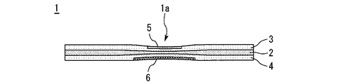
- FIG. 1 is a cross-sectional view showing a flexible substrate according to the first embodiment.
- FIG. 2 is a top view showing the flexible substrate according to the first embodiment.
- FIG. 3 is a bottom view showing the flexible substrate according to the first embodiment.
- the flexible substrate 1 is bent at bent portions 1a, 1b, and 1c, respectively, by a heat treatment described later.
- the base layer 2 has first and second main surfaces facing each other. First and second electrode patterns 3 and 4 are provided on the first and second main surfaces of the base layer 2, respectively.
- the base layer 2 is made of polyimide, and the first and second electrode patterns 3 and 4 are made of copper foil.
- the base layer 2 has a thickness of 50 ⁇ m and a width of 7 mm.
- the first and second electrode patterns 3 and 4 have a thickness of 20 ⁇ m.
- a heat shrink layer 5 is provided on the first electrode pattern 3, and a heat expansion layer 6 is provided on the second electrode pattern 4.
- the arrangement of the heat shrinkable layer 5 and the thermal expansion layer 6 is opposite to that of the bent portion 1a.
- the heat shrink layer 5 and the heat expansion layer 6 are disposed at positions facing each other on the first and second main surfaces of the flexible substrate, respectively, and the first and second electrode patterns 3 and 4 are arranged. Is housed in the recess.
- the thickness of the thermal contraction layer 5 and the thermal expansion layer 6 is 10 ⁇ m.
- the width dimensions of the heat-shrinkable layer 5 and the heat-expandable layer 6 are 1.4 mm at the bent portion 1a and 0.7 mm at the bent portions 1b and 1c.
- the heat-shrinkable layer 5 is made of a material that shrinks and cures with respect to the base layer 2 by heat treatment, for example, a polyolefin-based resin that has been subjected to radiation crosslinking and imparted heat-shrinkage characteristics.
- the thermal expansion layer 6 is made of a material that expands with respect to the base layer 2 by heat treatment, for example, a polyolefin-based resin. That is, the thermal contraction layer 5 and the thermal expansion layer 6 have different expansion coefficients. “Shrinkage coefficient” is defined by shrinkage, expansion, or dimensional change (JIS-C-2151, ASTM DDD-1204).
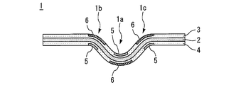
- FIG. 4 is a cross-sectional view showing a state in which the flexible substrate according to the first embodiment is bent.
- the heat-shrinkable layer 5 is contracted with respect to the base layer 2 by heat treatment using a soldering iron, and the thermal expansion layer 6 is expanded with respect to the base layer 2.
- the temperature of the heat treatment is about 120 ° C., and the treatment time is about 1 second for each bent portion.
- the heat treatment causes the flexible substrate 1 to bend with the heat shrinkable layer 5 on the inside and the heat expansion layer 6 on the outside.
- the bent portions 1a, 1b, and 1c can be formed into a smooth shape having an appropriate radius, and damage to the first and second electrode patterns 3 and 4 can be suppressed without applying extra stress. Also, manual bending can be simplified.
- a sufficient bending angle can be obtained even when the first and second electrode patterns 3 and 4 are provided on both surfaces. Moreover, a bending angle can be adjusted by changing the material, width dimension, or thickness of the heat contraction layer 5 and the thermal expansion layer 6.
- the bending direction can be reversed by reversing the surface of the flexible substrate 1 on which the heat shrink layer 5 and the heat expansion layer 6 are provided. Moreover, the flexible substrate 1 can be bent at a plurality of locations by providing the combination of the heat shrinkable layer 5 and the thermal expansion layer 6 at a plurality of locations.
- the width dimensions of the heat shrink layer 5 and the heat expansion layer 6 may be different from each other. Further, the bending angle is reduced by reducing the width dimension of the heat shrinkable layer 5 and the thermal expansion layer 6 as shown in FIG. 5, and the bending angle is increased by increasing the width dimension as shown in FIG.
- FIG. FIG. 7 is a sectional view showing a flexible substrate according to the second embodiment.
- the thickness of the bent portion 1a of the base layer 2 is 30 ⁇ m, which is thinner than the thickness of the base layer 2 other than the bent portion 1a. Thereby, it becomes easy to bend
- Other configurations and effects are the same as those of the first embodiment.
- FIG. 8 is a cross-sectional view showing a flexible substrate according to the third embodiment.
- FIG. 9 is a cross-sectional view showing a state in which the flexible substrate according to the third embodiment is bent.
- protective layers 7 and 8 that cover the first and second electrode patterns 3 and 4 are provided.
- the protective layers 7 and 8 are made of polyimide resin, for example.
- the heat-shrinkable layer 5 and the heat-expandable layer 6 are part of the protective layers 7 and 8, respectively. This eliminates the need for the concave portions of the first and second electrode patterns 3 and 4 that house the heat-shrinkable layer 5 and the heat-expandable layer 6, so there is no need to change the conventional pattern structure.
- Other configurations and effects are the same as those of the first embodiment.
Landscapes
- Engineering & Computer Science (AREA)
- Microelectronics & Electronic Packaging (AREA)
- Manufacturing & Machinery (AREA)
- Structure Of Printed Boards (AREA)
Abstract
フレキシブル基板(1)は折り曲げ部(1a)で折り曲げられる。ベース層(2)の第1及び第2の主面にそれぞれ第1及び第2の電極パターン(3,4)が設けられている。折り曲げ部(1a)において、加熱処理により収縮する材料からなる熱収縮層(5)が第1の電極パターン(3)の上に設けられ、加熱処理により膨張する材料からなる熱膨張層(6)が第2の電極パターン(4)の上に設けられている。
Description
本発明は、折り曲げ部で折り曲げられるフレキシブル基板に関する。
従来、曲げ金型をセットしたハンドプレス機を用いてフレキシブル基板を曲げ加工していた。しかし、折り目が付き、折り曲げ部を滑らかな形状にできなかった。また、曲げ金型による曲げ応力で電極パターンに断線又はピンホール等の損傷が発生して電気的にオープンとなり、必要な機能を発揮できなくなる場合もあった。これに対して、フレキシブル基板の折り曲げ部に熱収縮層を設け、加熱処理により熱収縮層を収縮させてフレキシブル基板を折り曲げる技術が開示されている(例えば、特許文献1参照)。
しかし、フレキシブル基板の両面に電極パターンがある場合、折り曲げ部に熱収縮層を設けただけでは十分な曲げ角度を得ることができず、曲げ角度の調整もできなかった。
本発明は、上述のような課題を解決するためになされたもので、その目的は折り曲げ部を滑らかな形状にでき、電極パターンの損傷を抑制でき、両面に電極パターンがある場合でも十分な曲げ角度を得ることができ、曲げ角度を調整することができるフレキシブル基板を得るものである。
本発明に係るフレキシブル基板は、折り曲げ部で折り曲げられるフレキシブル基板であって、互いに対向する第1及び第2の主面を有するベース層と、前記ベース層の前記第1及び第2の主面にそれぞれ設けられた第1及び第2の電極パターンと、前記折り曲げ部において前記第1の電極パターンの上に設けられ、加熱処理により収縮する材料からなる熱収縮層と、前記折り曲げ部において前記第2の電極パターンの上に設けられ、加熱処理により膨張する材料からなる熱膨張層とを備えることを特徴とする。
本発明では、加熱処理で折熱収縮層を収縮させ、熱膨張層を膨張させることでフレキシブル基板が折れ曲がる。これにより、折り曲げ部を適度な半径を持つ滑らかな形状にでき、余計なストレスを与えないことで電極パターンの損傷を抑制できる。熱収縮層及び熱膨張層の両方を用いることで両面に電極パターンがある場合でも十分な曲げ角度を得ることができる。熱収縮層及び熱膨張層の材質、幅寸法又は厚みを変更することで曲げ角度を調整することができる。
実施の形態に係るフレキシブル基板について図面を参照して説明する。同じ又は対応する構成要素には同じ符号を付し、説明の繰り返しを省略する場合がある。
実施の形態1.
図1は、実施の形態1に係るフレキシブル基板を示す断面図である。図2は、実施の形態1に係るフレキシブル基板を示す上面図である。図3は、実施の形態1に係るフレキシブル基板を示す下面図である。フレキシブル基板1は、後述の加熱処理により折り曲げ部1a,1b,1cでそれぞれ折り曲げられる。
図1は、実施の形態1に係るフレキシブル基板を示す断面図である。図2は、実施の形態1に係るフレキシブル基板を示す上面図である。図3は、実施の形態1に係るフレキシブル基板を示す下面図である。フレキシブル基板1は、後述の加熱処理により折り曲げ部1a,1b,1cでそれぞれ折り曲げられる。
ベース層2は互いに対向する第1及び第2の主面を有する。ベース層2の第1及び第2の主面にそれぞれ第1及び第2の電極パターン3,4が設けられている。ベース層2はポリイミドからなり、第1及び第2の電極パターン3,4は銅箔からなる。ベース層2の厚みは50μm、幅は7mmである。第1及び第2の電極パターン3,4の厚みは20μmである。
折り曲げ部1aにおいて、第1の電極パターン3の上に熱収縮層5が設けられ、第2の電極パターン4の上に熱膨張層6が設けられている。折り曲げ部1b,1cでは熱収縮層5と熱膨張層6の配置が折り曲げ部1aとは逆である。何れの折り曲げ部においても、熱収縮層5と熱膨張層6は、フレキシブル基板の第1及び第2の主面の互いに対向する位置にそれぞれ配置され、第1及び第2の電極パターン3,4の凹部に収納されている。熱収縮層5と熱膨張層6の厚みは10μmである。熱収縮層5と熱膨張層6の幅寸法は、折り曲げ部1aでは1.4mm、折り曲げ部1b,1cでは0.7mmである。
熱収縮層5は、加熱処理によりベース層2に対して収縮し硬化する材料、例えば放射線架橋し熱収縮特性を付与したポリオレフィン系樹脂からなる。熱膨張層6は、加熱処理によりベース層2に対して膨張する材料、例えばポリオレフィン系樹脂からなる。即ち、熱収縮層5と熱膨張層6は互いに伸縮係数が異なる。「収縮係数」は、収縮率、膨張率又は寸法変化率(JIS-C-2151、ASTMDD-1204)で定義される。
図4は、実施の形態1に係るフレキシブル基板が曲げられた状態を示す断面図である。ハンダコテを用いた加熱処理で熱収縮層5をベース層2に対して収縮させ、熱膨張層6をベース層2に対して膨張させる。加熱処理の温度は約120℃、処理時間は各折り曲げ部につき約1秒である。
この加熱処理により熱収縮層5を内側に、熱膨張層6を外側にしてフレキシブル基板1が折れ曲がる。これにより、折り曲げ部1a,1b,1cを適度な半径を持つ滑らかな形状にでき、余計なストレスを与えないことで第1及び第2の電極パターン3,4の損傷を抑制できる。また、手作業による曲げ加工を簡略化することができる。
熱収縮層5及び熱膨張層6の両方を用いることで両面に第1及び第2の電極パターン3,4がある場合でも十分な曲げ角度を得ることができる。また、熱収縮層5及び熱膨張層6の材質、幅寸法又は厚みを変更することで曲げ角度を調整することができる。
熱収縮層5及び熱膨張層6を設けるフレキシブル基板1の面を逆にすることで曲げ方向を逆にすることができる。また、熱収縮層5及び熱膨張層6の組み合わせを複数個所に設けることで、複数箇所でフレキシブル基板1を折り曲げることができる。
図5及び図6は、実施の形態1に係るフレキシブル基板の変形例を示す断面図である。このように熱収縮層5と熱膨張層6の幅寸法は互いに異なっていてもよい。また、図5のように熱収縮層5及び熱膨張層6の幅寸法を狭くすることで曲げ角度が小さくなり、図6のように幅寸法を広くすることで曲げ角度が大きくなる。
実施の形態2.
図7は、実施の形態2に係るフレキシブル基板を示す断面図である。本実施の形態では、ベース層2の折り曲げ部1aでの厚みは30μmであり、ベース層2の折り曲げ部1a以外での厚み50μmに比べて薄い。これにより、折り曲げ部1aで折り曲げやすくなる。その他の構成及び効果は実施の形態1と同様である。
図7は、実施の形態2に係るフレキシブル基板を示す断面図である。本実施の形態では、ベース層2の折り曲げ部1aでの厚みは30μmであり、ベース層2の折り曲げ部1a以外での厚み50μmに比べて薄い。これにより、折り曲げ部1aで折り曲げやすくなる。その他の構成及び効果は実施の形態1と同様である。
実施の形態3.
図8は、実施の形態3に係るフレキシブル基板を示す断面図である。図9は、実施の形態3に係るフレキシブル基板が曲げられた状態を示す断面図である。本実施の形態では、第1及び第2の電極パターン3,4をそれぞれ覆う保護層7,8が設けられている。保護層7,8は例えばポリイミド樹脂からなる。熱収縮層5及び熱膨張層6はそれぞれ保護層7,8の一部である。これにより、熱収縮層5及び熱膨張層6を収納する第1及び第2の電極パターン3,4の凹部が不要となるため、従来のパターン構造を変更する必要がない。その他の構成及び効果は実施の形態1と同様である。
図8は、実施の形態3に係るフレキシブル基板を示す断面図である。図9は、実施の形態3に係るフレキシブル基板が曲げられた状態を示す断面図である。本実施の形態では、第1及び第2の電極パターン3,4をそれぞれ覆う保護層7,8が設けられている。保護層7,8は例えばポリイミド樹脂からなる。熱収縮層5及び熱膨張層6はそれぞれ保護層7,8の一部である。これにより、熱収縮層5及び熱膨張層6を収納する第1及び第2の電極パターン3,4の凹部が不要となるため、従来のパターン構造を変更する必要がない。その他の構成及び効果は実施の形態1と同様である。
1 フレキシブル基板、1a,1b,1c 折り曲げ部、2 ベース層、3 第1の電極パターン、4 第2の電極パターン、5 熱収縮層、6 熱膨張層、7,8 保護層
Claims (3)
- 折り曲げ部で折り曲げられるフレキシブル基板であって、
互いに対向する第1及び第2の主面を有するベース層と、
前記ベース層の前記第1及び第2の主面にそれぞれ設けられた第1及び第2の電極パターンと、
前記折り曲げ部において前記第1の電極パターンの上に設けられ、加熱処理により収縮する材料からなる熱収縮層と、
前記折り曲げ部において前記第2の電極パターンの上に設けられ、加熱処理により膨張する材料からなる熱膨張層とを備えることを特徴とするフレキシブル基板。 - 前記ベース層の前記折り曲げ部での厚みは、前記ベース層の前記折り曲げ部以外での厚みに比べて薄いことを特徴とする請求項1に記載のフレキシブル基板。
- 前記第1及び第2の電極パターンをそれぞれ覆う保護層を更に備え、
前記熱収縮層及び前記熱膨張層は前記保護層の一部であることを特徴とする請求項1又は2に記載のフレキシブル基板。
Priority Applications (1)
| Application Number | Priority Date | Filing Date | Title |
|---|---|---|---|
| PCT/JP2018/005559 WO2019159337A1 (ja) | 2018-02-16 | 2018-02-16 | フレキシブル基板 |
Applications Claiming Priority (1)
| Application Number | Priority Date | Filing Date | Title |
|---|---|---|---|
| PCT/JP2018/005559 WO2019159337A1 (ja) | 2018-02-16 | 2018-02-16 | フレキシブル基板 |
Publications (1)
| Publication Number | Publication Date |
|---|---|
| WO2019159337A1 true WO2019159337A1 (ja) | 2019-08-22 |
Family
ID=67619791
Family Applications (1)
| Application Number | Title | Priority Date | Filing Date |
|---|---|---|---|
| PCT/JP2018/005559 Ceased WO2019159337A1 (ja) | 2018-02-16 | 2018-02-16 | フレキシブル基板 |
Country Status (1)
| Country | Link |
|---|---|
| WO (1) | WO2019159337A1 (ja) |
Cited By (1)
| Publication number | Priority date | Publication date | Assignee | Title |
|---|---|---|---|---|
| CN114964400A (zh) * | 2022-06-14 | 2022-08-30 | 南京高华科技股份有限公司 | 流量传感器及其制作方法 |
Citations (3)
| Publication number | Priority date | Publication date | Assignee | Title |
|---|---|---|---|---|
| JPH01255286A (ja) * | 1988-04-05 | 1989-10-12 | Canon Inc | 成形フレキシブルプリント基板 |
| JPH04112594A (ja) * | 1990-08-31 | 1992-04-14 | Sharp Corp | 折り曲げ可能なフレキシブル基板及びその加工方法 |
| JPH07312469A (ja) * | 1994-05-16 | 1995-11-28 | Nippon Mektron Ltd | 多層フレキシブル回路基板の屈曲部構造 |
-
2018
- 2018-02-16 WO PCT/JP2018/005559 patent/WO2019159337A1/ja not_active Ceased
Patent Citations (3)
| Publication number | Priority date | Publication date | Assignee | Title |
|---|---|---|---|---|
| JPH01255286A (ja) * | 1988-04-05 | 1989-10-12 | Canon Inc | 成形フレキシブルプリント基板 |
| JPH04112594A (ja) * | 1990-08-31 | 1992-04-14 | Sharp Corp | 折り曲げ可能なフレキシブル基板及びその加工方法 |
| JPH07312469A (ja) * | 1994-05-16 | 1995-11-28 | Nippon Mektron Ltd | 多層フレキシブル回路基板の屈曲部構造 |
Cited By (1)
| Publication number | Priority date | Publication date | Assignee | Title |
|---|---|---|---|---|
| CN114964400A (zh) * | 2022-06-14 | 2022-08-30 | 南京高华科技股份有限公司 | 流量传感器及其制作方法 |
Similar Documents
| Publication | Publication Date | Title |
|---|---|---|
| CN107432080B (zh) | 挠性印刷线路板 | |
| US20160365170A1 (en) | Protector and wire harness | |
| WO2016024415A1 (ja) | 伸縮性フレキシブルプリント基板および伸縮性フレキシブルプリント基板の製造方法 | |
| KR20190132745A (ko) | 스트레쳐블 디스플레이 및 그 제조방법 | |
| WO2019159337A1 (ja) | フレキシブル基板 | |
| JP2009081357A5 (ja) | ||
| JP2016018813A (ja) | 熱輸送シートおよびその製造方法 | |
| WO2020110422A1 (ja) | フレキシブル基板 | |
| JP4950923B2 (ja) | 伸縮型プリント配線板 | |
| JP2008300681A (ja) | プリント配線基板 | |
| JP6365360B2 (ja) | 電子装置及びその製造方法 | |
| WO2016043136A1 (ja) | 表示装置及びその製造方法 | |
| JP4330950B2 (ja) | 電気回路複合モジュール | |
| JP7056853B2 (ja) | Mems素子の実装構造 | |
| CN210518977U (zh) | 一种能提高表面贴装器件焊点可靠性的低应力印刷电路板 | |
| JP6832514B2 (ja) | コンデンサおよびコンデンサの製造方法 | |
| JP2016152749A (ja) | ワイヤーハーネス | |
| JP2022051283A5 (ja) | ||
| JP2006165389A (ja) | プリント基板 | |
| TWI905818B (zh) | 電路板及其製造方法 | |
| JP6674839B2 (ja) | 回路基板製造方法 | |
| CN114521044B (zh) | 电路板及其电器装置 | |
| TW202115542A (zh) | 絕緣膠保護的改良結構 | |
| WO2019159505A1 (ja) | 伸縮性基板およびその製造方法 | |
| JP2021524674A (ja) | 伸縮可能な電子デバイス |
Legal Events
| Date | Code | Title | Description |
|---|---|---|---|
| 121 | Ep: the epo has been informed by wipo that ep was designated in this application |
Ref document number: 18906239 Country of ref document: EP Kind code of ref document: A1 |
|
| NENP | Non-entry into the national phase |
Ref country code: DE |
|
| 122 | Ep: pct application non-entry in european phase |
Ref document number: 18906239 Country of ref document: EP Kind code of ref document: A1 |
|
| NENP | Non-entry into the national phase |
Ref country code: JP |