WO2019131963A1 - 回路付きフィルム - Google Patents
回路付きフィルム Download PDFInfo
- Publication number
- WO2019131963A1 WO2019131963A1 PCT/JP2018/048359 JP2018048359W WO2019131963A1 WO 2019131963 A1 WO2019131963 A1 WO 2019131963A1 JP 2018048359 W JP2018048359 W JP 2018048359W WO 2019131963 A1 WO2019131963 A1 WO 2019131963A1
- Authority
- WO
- WIPO (PCT)
- Prior art keywords
- circuit
- film
- resin film
- conductive
- resin
- Prior art date
- Legal status (The legal status is an assumption and is not a legal conclusion. Google has not performed a legal analysis and makes no representation as to the accuracy of the status listed.)
- Ceased
Links
Images






Classifications
-
- B—PERFORMING OPERATIONS; TRANSPORTING
- B32—LAYERED PRODUCTS
- B32B—LAYERED PRODUCTS, i.e. PRODUCTS BUILT-UP OF STRATA OF FLAT OR NON-FLAT, e.g. CELLULAR OR HONEYCOMB, FORM
- B32B15/00—Layered products comprising a layer of metal
- B32B15/04—Layered products comprising a layer of metal comprising metal as the main or only constituent of a layer, which is next to another layer of the same or of a different material
- B32B15/08—Layered products comprising a layer of metal comprising metal as the main or only constituent of a layer, which is next to another layer of the same or of a different material of synthetic resin
-
- B—PERFORMING OPERATIONS; TRANSPORTING
- B32—LAYERED PRODUCTS
- B32B—LAYERED PRODUCTS, i.e. PRODUCTS BUILT-UP OF STRATA OF FLAT OR NON-FLAT, e.g. CELLULAR OR HONEYCOMB, FORM
- B32B17/00—Layered products essentially comprising sheet glass, or glass, slag, or like fibres
- B32B17/06—Layered products essentially comprising sheet glass, or glass, slag, or like fibres comprising glass as the main or only constituent of a layer, next to another layer of a specific material
- B32B17/10—Layered products essentially comprising sheet glass, or glass, slag, or like fibres comprising glass as the main or only constituent of a layer, next to another layer of a specific material of synthetic resin
- B32B17/10005—Layered products essentially comprising sheet glass, or glass, slag, or like fibres comprising glass as the main or only constituent of a layer, next to another layer of a specific material of synthetic resin laminated safety glass or glazing
- B32B17/10165—Functional features of the laminated safety glass or glazing
- B32B17/10376—Laminated safety glass or glazing containing metal wires
- B32B17/10385—Laminated safety glass or glazing containing metal wires for ohmic resistance heating
-
- B—PERFORMING OPERATIONS; TRANSPORTING
- B32—LAYERED PRODUCTS
- B32B—LAYERED PRODUCTS, i.e. PRODUCTS BUILT-UP OF STRATA OF FLAT OR NON-FLAT, e.g. CELLULAR OR HONEYCOMB, FORM
- B32B17/00—Layered products essentially comprising sheet glass, or glass, slag, or like fibres
- B32B17/06—Layered products essentially comprising sheet glass, or glass, slag, or like fibres comprising glass as the main or only constituent of a layer, next to another layer of a specific material
- B32B17/10—Layered products essentially comprising sheet glass, or glass, slag, or like fibres comprising glass as the main or only constituent of a layer, next to another layer of a specific material of synthetic resin
- B32B17/10005—Layered products essentially comprising sheet glass, or glass, slag, or like fibres comprising glass as the main or only constituent of a layer, next to another layer of a specific material of synthetic resin laminated safety glass or glazing
- B32B17/1055—Layered products essentially comprising sheet glass, or glass, slag, or like fibres comprising glass as the main or only constituent of a layer, next to another layer of a specific material of synthetic resin laminated safety glass or glazing characterized by the resin layer, i.e. interlayer
- B32B17/10605—Type of plasticiser
-
- B—PERFORMING OPERATIONS; TRANSPORTING
- B32—LAYERED PRODUCTS
- B32B—LAYERED PRODUCTS, i.e. PRODUCTS BUILT-UP OF STRATA OF FLAT OR NON-FLAT, e.g. CELLULAR OR HONEYCOMB, FORM
- B32B17/00—Layered products essentially comprising sheet glass, or glass, slag, or like fibres
- B32B17/06—Layered products essentially comprising sheet glass, or glass, slag, or like fibres comprising glass as the main or only constituent of a layer, next to another layer of a specific material
- B32B17/10—Layered products essentially comprising sheet glass, or glass, slag, or like fibres comprising glass as the main or only constituent of a layer, next to another layer of a specific material of synthetic resin
- B32B17/10005—Layered products essentially comprising sheet glass, or glass, slag, or like fibres comprising glass as the main or only constituent of a layer, next to another layer of a specific material of synthetic resin laminated safety glass or glazing
- B32B17/1055—Layered products essentially comprising sheet glass, or glass, slag, or like fibres comprising glass as the main or only constituent of a layer, next to another layer of a specific material of synthetic resin laminated safety glass or glazing characterized by the resin layer, i.e. interlayer
- B32B17/10761—Layered products essentially comprising sheet glass, or glass, slag, or like fibres comprising glass as the main or only constituent of a layer, next to another layer of a specific material of synthetic resin laminated safety glass or glazing characterized by the resin layer, i.e. interlayer containing vinyl acetal
-
- B—PERFORMING OPERATIONS; TRANSPORTING
- B32—LAYERED PRODUCTS
- B32B—LAYERED PRODUCTS, i.e. PRODUCTS BUILT-UP OF STRATA OF FLAT OR NON-FLAT, e.g. CELLULAR OR HONEYCOMB, FORM
- B32B27/00—Layered products comprising a layer of synthetic resin
- B32B27/28—Layered products comprising a layer of synthetic resin comprising synthetic resins not wholly covered by any one of the sub-groups B32B27/30 - B32B27/42
-
- B—PERFORMING OPERATIONS; TRANSPORTING
- B60—VEHICLES IN GENERAL
- B60J—WINDOWS, WINDSCREENS, NON-FIXED ROOFS, DOORS, OR SIMILAR DEVICES FOR VEHICLES; REMOVABLE EXTERNAL PROTECTIVE COVERINGS SPECIALLY ADAPTED FOR VEHICLES
- B60J1/00—Windows; Windscreens; Accessories therefor
-
- C—CHEMISTRY; METALLURGY
- C08—ORGANIC MACROMOLECULAR COMPOUNDS; THEIR PREPARATION OR CHEMICAL WORKING-UP; COMPOSITIONS BASED THEREON
- C08L—COMPOSITIONS OF MACROMOLECULAR COMPOUNDS
- C08L29/00—Compositions of homopolymers or copolymers of compounds having one or more unsaturated aliphatic radicals, each having only one carbon-to-carbon double bond, and at least one being terminated by an alcohol, ether, aldehydo, ketonic, acetal or ketal radical; Compositions of hydrolysed polymers of esters of unsaturated alcohols with saturated carboxylic acids; Compositions of derivatives of such polymers
- C08L29/14—Homopolymers or copolymers of acetals or ketals obtained by polymerisation of unsaturated acetals or ketals or by after-treatment of polymers of unsaturated alcohols
-
- H—ELECTRICITY
- H01—ELECTRIC ELEMENTS
- H01B—CABLES; CONDUCTORS; INSULATORS; SELECTION OF MATERIALS FOR THEIR CONDUCTIVE, INSULATING OR DIELECTRIC PROPERTIES
- H01B1/00—Conductors or conductive bodies characterised by the conductive materials; Selection of materials as conductors
- H01B1/02—Conductors or conductive bodies characterised by the conductive materials; Selection of materials as conductors mainly consisting of metals or alloys
-
- H—ELECTRICITY
- H01—ELECTRIC ELEMENTS
- H01B—CABLES; CONDUCTORS; INSULATORS; SELECTION OF MATERIALS FOR THEIR CONDUCTIVE, INSULATING OR DIELECTRIC PROPERTIES
- H01B5/00—Non-insulated conductors or conductive bodies characterised by their form
- H01B5/14—Non-insulated conductors or conductive bodies characterised by their form comprising conductive layers or films on insulating-supports
-
- H—ELECTRICITY
- H01—ELECTRIC ELEMENTS
- H01Q—ANTENNAS, i.e. RADIO AERIALS
- H01Q1/00—Details of, or arrangements associated with, antennas
- H01Q1/36—Structural form of radiating elements, e.g. cone, spiral, umbrella; Particular materials used therewith
- H01Q1/38—Structural form of radiating elements, e.g. cone, spiral, umbrella; Particular materials used therewith formed by a conductive layer on an insulating support
-
- H—ELECTRICITY
- H05—ELECTRIC TECHNIQUES NOT OTHERWISE PROVIDED FOR
- H05B—ELECTRIC HEATING; ELECTRIC LIGHT SOURCES NOT OTHERWISE PROVIDED FOR; CIRCUIT ARRANGEMENTS FOR ELECTRIC LIGHT SOURCES, IN GENERAL
- H05B1/00—Details of electric heating devices
- H05B1/02—Automatic switching arrangements specially adapted to apparatus ; Control of heating devices
- H05B1/0227—Applications
- H05B1/023—Industrial applications
- H05B1/0236—Industrial applications for vehicles
-
- H—ELECTRICITY
- H05—ELECTRIC TECHNIQUES NOT OTHERWISE PROVIDED FOR
- H05B—ELECTRIC HEATING; ELECTRIC LIGHT SOURCES NOT OTHERWISE PROVIDED FOR; CIRCUIT ARRANGEMENTS FOR ELECTRIC LIGHT SOURCES, IN GENERAL
- H05B3/00—Ohmic-resistance heating
- H05B3/20—Heating elements having extended surface area substantially in a two-dimensional [2D] plane, e.g. plate-heater
-
- H—ELECTRICITY
- H05—ELECTRIC TECHNIQUES NOT OTHERWISE PROVIDED FOR
- H05B—ELECTRIC HEATING; ELECTRIC LIGHT SOURCES NOT OTHERWISE PROVIDED FOR; CIRCUIT ARRANGEMENTS FOR ELECTRIC LIGHT SOURCES, IN GENERAL
- H05B3/00—Ohmic-resistance heating
- H05B3/84—Heating arrangements specially adapted for transparent or reflecting areas, e.g. for demisting or de-icing windows, mirrors or vehicle windshields
- H05B3/86—Heating arrangements specially adapted for transparent or reflecting areas, e.g. for demisting or de-icing windows, mirrors or vehicle windshields the heating conductors being embedded in the transparent or reflecting material
-
- H—ELECTRICITY
- H05—ELECTRIC TECHNIQUES NOT OTHERWISE PROVIDED FOR
- H05B—ELECTRIC HEATING; ELECTRIC LIGHT SOURCES NOT OTHERWISE PROVIDED FOR; CIRCUIT ARRANGEMENTS FOR ELECTRIC LIGHT SOURCES, IN GENERAL
- H05B2203/00—Aspects relating to Ohmic resistive heating covered by group H05B3/00
- H05B2203/013—Heaters using resistive films or coatings
-
- H—ELECTRICITY
- H05—ELECTRIC TECHNIQUES NOT OTHERWISE PROVIDED FOR
- H05B—ELECTRIC HEATING; ELECTRIC LIGHT SOURCES NOT OTHERWISE PROVIDED FOR; CIRCUIT ARRANGEMENTS FOR ELECTRIC LIGHT SOURCES, IN GENERAL
- H05B2203/00—Aspects relating to Ohmic resistive heating covered by group H05B3/00
- H05B2203/016—Heaters using particular connecting means
-
- H—ELECTRICITY
- H05—ELECTRIC TECHNIQUES NOT OTHERWISE PROVIDED FOR
- H05B—ELECTRIC HEATING; ELECTRIC LIGHT SOURCES NOT OTHERWISE PROVIDED FOR; CIRCUIT ARRANGEMENTS FOR ELECTRIC LIGHT SOURCES, IN GENERAL
- H05B2203/00—Aspects relating to Ohmic resistive heating covered by group H05B3/00
- H05B2203/035—Electrical circuits used in resistive heating apparatus
Definitions
- the present invention relates to a film with a circuit used for laminated glass and a laminated glass having the film with the circuit.
- Patent Document 1 a plurality of heaters (a wire heater and a surface heater) for heating a glass plate, which are arranged to divide a glass plate surface into a plurality of places between two glass plates, and an end portion of the heater
- a heating window is disclosed which includes a plurality of bus bars which are provided to energize the heater.
- the heating window glass can heat each heater individually or in combination.
- Patent Document 1 when a wire heater or a surface heater is used as the heater, the forward visibility is significantly deteriorated. It was found that a conductive fine line circuit having a small line width can be used to improve the forward visibility, but the conductive fine line circuit is likely to be broken at the time of producing a laminated glass.
- an object of the present invention is to provide a film with a circuit which is free from breakage during the production of laminated glass and is excellent in forward visibility even after the production of laminated glass and which allows current to flow individually to a plurality of conductive circuits. It is. Another object of the present invention is to provide a laminated glass which has no disconnection and has excellent front visibility, and in which current can be individually supplied to a plurality of conductive circuits.
- the present invention includes the following.
- [1] A film with a circuit having a conductive fine wire circuit (A), a resin film (1), and a conductive circuit (B) in this order.
- [2] The film with a circuit according to [1], wherein the conductive fine wire circuit (A) and / or the conductive circuit (B) is a circuit derived from a metal foil.
- a conductive circuit (B) is formed on one surface of another resin film (1) different from the conductive film, and a conductive thin circuit (A) having the resin film (1) and a conductive circuit having the resin film (1)
- the manufacturing method of the film with a circuit including process (i) which obtains (B).
- the film with circuit of the present invention does not cause breakage during the production of laminated glass, has excellent forward visibility, and can flow current individually to a plurality of conductive circuits.
- the laminated glass of the present invention has no breakage, has excellent front visibility, and can flow current individually to a plurality of conductive circuits.
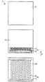
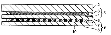
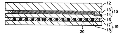
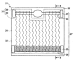
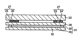
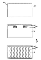
- FIG. 1A It is an exploded plan view showing one embodiment of a film with a circuit of the present invention. It is a top view of the film with a circuit shown to FIG. 1A. It is the II-II sectional view taken on the line of a film with a circuit shown in Drawing 1B. It is an exploded plan view showing one embodiment of a film with a circuit of the present invention. It is a top view of the film with a circuit shown to FIG. 2A. It is the II-II sectional view taken on the line of a film with a circuit shown in Drawing 2B. It is an exploded plan view showing one embodiment of a film with a circuit of the present invention. It is a top view of the film with a circuit shown to FIG. 3A.
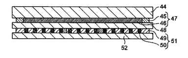
- FIG. 5A is a cross-sectional view of the film with circuit shown in FIG. 5B taken along line II-II.
- the film with circuit of the present invention has a conductive fine wire circuit (A), a resin film (1), and a conductive circuit (B) in this order.
- the film with circuit of the present invention has one or more resin films (1).
- the resin contained in the resin film (1) include polyvinyl acetal resin, ionomer resin, ethylene vinyl acetate copolymer resin, styrene-butadiene copolymer and the like.
- the resin film (1) is at least one selected from the group consisting of polyvinyl acetal resin, ionomer resin and ethylene vinyl acetate copolymer resin from the viewpoint of effectively preventing peeling and deformation of the circuit at the time of laminated glass production. It is preferred to contain a resin of the kind.
- polyvinyl acetal resin polyvinyl acetal resin manufactured by acetalization of vinyl alcohol-type resin, such as polyvinyl alcohol or a vinyl alcohol copolymer, is mentioned, for example.
- the resin film (1) may contain one type of polyvinyl acetal resin, and the viscosity average degree of polymerization, the degree of acetalization, the amount of acetyl groups, the amount of hydroxyl groups, the amount of hydroxyl groups, ethylene content, acetalization
- Two or more polyvinyl acetal resins in which one or more of the molecular weight and the chain length of the aldehyde used for each may be different may be included.
- the polyvinyl acetal resin contains two or more different polyvinyl acetals, the viscosity average degree of polymerization, the degree of acetalization, the amount of acetyl groups, the amount of hydroxyl groups, or two or more of the polyvinyl acetal resins It is preferable that it is a mixture from the viewpoint of ease of melt forming, from the viewpoint of suppressing breakage or deformation at the time of producing laminated glass, and from the viewpoint of preventing deviation of glass at the time of using laminated glass.
- the polyvinyl acetal resin used in the present invention can be produced, for example, by the following method, but is not limited thereto.
- an aldehyde (or keto compound) and an acid catalyst are added, and the acetalization reaction is carried out for 30 to 300 minutes while keeping the temperature constant.
- the reaction solution is heated to a temperature of 20 to 80 ° C. for 30 to 200 minutes, and held for 30 to 300 minutes. Thereafter, the reaction solution is filtered if necessary, and then neutralized by adding a neutralizing agent such as alkali, and the resin is filtered, washed with water and dried to obtain a polyvinyl acetal resin.
- the acid catalyst used for the acetalization reaction is not particularly limited, and any of organic acids and inorganic acids can be used, and examples thereof include acetic acid, p-toluenesulfonic acid, nitric acid, sulfuric acid and hydrochloric acid. Among them, hydrochloric acid, sulfuric acid and nitric acid are preferable from the viewpoint of the strength of the acid and the ease of removal at the time of washing.
- the vinyl alcohol copolymer is obtained by saponifying a copolymer of a vinyl ester and another monomer.
- Other monomers include, for example, ⁇ -olefins such as ethylene, propylene, n-butene and isobutylene; acrylic acid and salts thereof; methyl acrylate, ethyl acrylate, n-propyl acrylate, i-propyl acrylate Acrylic acid esters such as n-butyl acrylate, i-butyl acrylate, t-butyl acrylate, 2-ethylhexyl acrylate, dodecyl acrylate, octadecyl acrylate, etc .; methacrylic acid and salts thereof; methyl methacrylate, methacrylic Ethyl methacrylate, n-propyl methacrylate, i-propyl methacrylate, n-butyl methacrylate, i-buty
- the aldehyde (or keto compound) used for producing the polyvinyl acetal resin is a linear, branched or cyclic one having 1 to 10 carbon atoms. It is preferably present, and more preferably linear or branched. This gives the corresponding linear or branched acetal group.
- the polyvinyl acetal resin used in the present invention may be obtained by acetalizing polyvinyl alcohol or a vinyl alcohol copolymer with a mixture of a plurality of aldehydes (or keto compounds).
- the polyvinyl alcohol or the vinyl alcohol copolymer may be composed of only one of them, or may be a mixture of polyvinyl alcohol and a vinyl alcohol copolymer.
- the polyvinyl acetal resin used in the present invention is preferably produced by the reaction of at least one polyvinyl alcohol and one or more aldehydes having 1 to 10 carbon atoms. If the number of carbon atoms of the aldehyde exceeds 11, the reactivity of acetalization decreases, and furthermore, blocks of the polyvinyl acetal resin are easily generated during the reaction, and the synthesis of the polyvinyl acetal resin tends to be difficult.
- aldehydes examples include formaldehyde, acetaldehyde, propionaldehyde, n-butyraldehyde, isobutyraldehyde, valeraldehyde, isovaleraldehyde, n-hexyl aldehyde, 2-ethylbutyraldehyde, n-heptyl aldehyde, n-octyl aldehyde, 2 And aliphatic, aromatic and alicyclic aldehydes such as ethylhexyl aldehyde, n-nonyl aldehyde, n-decyl aldehyde, benzaldehyde and cinnamaldehyde.
- aldehydes having 2 to 6 carbon atoms are preferable, and n-butyraldehyde is particularly preferable from the viewpoint of easily obtaining a polyvinyl acetal resin having a suitable breaking energy.
- aldehydes can be used alone or in combination of two or more. Furthermore, you may use together the aldehyde etc. which have a polyfunctional aldehyde and another functional group in the range of 20 mass% or less of all the aldehydes.
- the content of n-butyraldehyde in the aldehyde used for acetalization is preferably 50% by mass or more, more preferably 80% by mass or more, still more preferably 95% by mass or more, and 99% by mass
- the above is particularly preferable, and it may be 100% by mass.
- the viscosity average polymerization degree of polyvinyl alcohol is preferably 5000 or less, more preferably 3000 or less, still more preferably 2500 or less, particularly preferably 2300 or less, and most preferably 2000 or less.
- the viscosity average polymerization degree of polyvinyl alcohol is less than or equal to the above upper limit value, it is easy to obtain a good film forming property.
- the viscosity average polymerization degree of polyvinyl alcohol can be measured, for example, based on JIS K 6726 "Polyvinyl alcohol test method".
- the viscosity average polymerization degree of the polyvinyl acetal resin coincides with the viscosity average polymerization degree of the polyvinyl alcohol as a raw material, so the preferable viscosity average polymerization degree of the polyvinyl alcohol described above coincides with the preferable viscosity average polymerization degree of the polyvinyl acetal resin .
- the resin film (1) contains two or more different polyvinyl acetal resins, it is preferable that the viscosity average degree of polymerization of at least one polyvinyl acetal resin is not less than the lower limit value and not more than the upper limit value.
- the amount of acetyl groups in the polyvinyl acetal resin constituting the resin film (1) is preferably 0.01 to 20% by mass, more preferably 0.05 to 10% by mass, based on the ethylene unit of the polyvinyl acetal main chain. More preferably, it is 0.1 to 5% by mass.
- the amount of acetyl groups of the polyvinyl acetal resin can be adjusted by appropriately adjusting the degree of saponification of the polyvinyl alcohol or vinyl alcohol copolymer as a raw material.
- the amount of acetyl group affects the polarity of the polyvinyl acetal resin, which may change the plasticizer compatibility and mechanical strength of the resin film (1).
- the resin film (1) contains a polyvinyl acetal resin in which the amount of acetyl groups is within the above range, it is easy to achieve reduction of optical distortion and the like.
- the resin film (1) contains two or more different polyvinyl acetal resins, the amount of acetyl groups of at least one polyvinyl acetal resin is preferably within the above range.
- the degree of acetalization of the polyvinyl acetal resin used in the present invention is not particularly limited, but is preferably 40 to 86% by mass, more preferably 45 to 84% by mass, still more preferably 50 to 82% by mass, and particularly preferably 60 to 82% by mass Preferably, 68 to 82% by weight is most preferred.
- the degree of acetalization of the polyvinyl acetal resin can be adjusted within the above range by appropriately adjusting the amount of aldehyde used in acetalizing the polyvinyl alcohol resin. When the degree of acetalization is in the above range, the mechanical strength of the laminated glass of the present invention tends to be sufficient, and the compatibility between the polyvinyl acetal resin and the plasticizer is unlikely to be reduced.
- the resin film (1) contains two or more different polyvinyl acetal resins, the degree of acetalization of at least one polyvinyl acetal resin is preferably within the above range.
- the amount of hydroxyl groups of the polyvinyl acetal resin is preferably 6 to 26% by mass, more preferably 12 to 24% by mass, more preferably 15 to 22% by mass, particularly preferably 18 to 22% by mass, based on the ethylene unit of the polyvinyl acetal main chain. It is 21% by mass.
- the preferable range for imparting the sound insulation performance is 6 to 20% by mass, more preferably 8 to 18% by mass, still more preferably 10 to 15% by mass, and particularly preferably 11 to 13% by mass.
- the amount of hydroxyl groups can be adjusted within the above range by adjusting the amount of aldehyde used in acetalizing the polyvinyl alcohol resin.
- the amount of hydroxyl groups is within the above range, the difference in refractive index with the resin film (2) described later becomes small, and it is easy to obtain laminated glass with little optical unevenness.
- the resin film (1) contains two or more different polyvinyl acetal resins, the amount of hydroxyl groups of at least one polyvinyl acetal resin is preferably in the above range.
- the polyvinyl acetal resin is usually composed of an acetal group unit, a hydroxyl group unit and an acetyl group unit, and the amount of each unit thereof is measured by, for example, JIS K 6728 "polyvinyl butyral test method" or nuclear magnetic resonance method (NMR) it can. Moreover, when polyvinyl acetal resin contains units other than an acetal group unit, the unit amount of a hydroxyl group and the unit amount of an acetyl group are measured, and the acetal in the case where these unit amounts do not contain units other than an acetal group unit. By subtracting from the base unit amount, the remaining acetal group unit amount can be calculated.
- the resin film (1) preferably contains uncrosslinked polyvinyl acetal from the viewpoint of easily obtaining good film formability, but may also contain crosslinked polyvinyl acetal.
- Methods for crosslinking polyvinyl acetals are described, for example, in EP 1527107 B1 and WO 2004/063231 A1 (thermal self-crosslinking of carboxyl group-containing polyvinyl acetals), EP 16063 25 A1 (polyaldehydes crosslinked with polyaldehydes), and WO 2003/020776 A1 Glyoxylic acid crosslinked polyvinyl acetals).
- it is also a useful method to control the amount of inter-acetal acetal bond to be generated by adjusting the acetalization reaction conditions appropriately, or to control the degree of blocking of the remaining hydroxyl groups.
- the ionomer resin is not particularly limited, but it has a structural unit derived from an olefin such as ethylene and a structural unit derived from an ⁇ , ⁇ -unsaturated carboxylic acid, and at least a portion of the ⁇ , ⁇ -unsaturated carboxylic acid is a metal
- the thermoplastic resin neutralized by the ion is mentioned.
- the metal ion include alkali metal ions such as sodium ion; alkaline earth metal ions such as magnesium ion; zinc ion and the like.
- the content of the structural unit of the ⁇ , ⁇ -unsaturated carboxylic acid is the ethylene- ⁇ , ⁇ -unsaturated carboxylic acid 2 mass% or more is preferable based on the mass of an acid copolymer, and 5 mass% or more is more preferable.
- the content of the structural unit of the ⁇ , ⁇ -unsaturated carboxylic acid is preferably 30% by mass or less, and more preferably 20% by mass or less.
- Examples of the structural unit derived from the ⁇ , ⁇ -unsaturated carboxylic acid possessed by the ionomer resin include structural units derived from acrylic acid, methacrylic acid, maleic acid, monomethyl maleate, monoethyl maleate, and maleic anhydride. Among them, structural units derived from acrylic acid or methacrylic acid are particularly preferred.
- the ionomer resin is preferably an ionomer of ethylene-acrylic acid copolymer and an ionomer of ethylene-methacrylic acid copolymer from the viewpoint of easy availability, and a zinc ionomer of ethylene-acrylic acid copolymer, ethylene-acrylic Particularly preferred are sodium ionomers of acid copolymers, zinc ionomers of ethylene-methacrylic acid copolymers, and sodium ionomers of ethylene-methacrylic acid copolymers.
- the ionomer resins can be used alone or in combination of two or more.
- the ratio of vinyl acetate units to the total of ethylene units and vinyl acetate units is preferably less than 50 mol%, more preferably less than 30 mol%, still more preferably less than 20 mol%, 15 mol% Less than is particularly preferred. If the proportion of vinyl acetate units to the total of ethylene units and vinyl acetate units is less than 50 mol%, the mechanical strength and flexibility required for the resin film (1) contained in the film with a circuit used for laminated glass are suitable Tend to be expressed in
- the resin film (1) is preferably 50% by mass or more, more preferably 70% by mass or more, still more preferably 90% by mass or more, particularly preferably 100% by mass of polyvinyl acetal based on the mass of the resin film (1) It is preferred to contain a resin.
- a resin When the content of the polyvinyl acetal resin in the resin film (1) is in the above range, breakage, deformation and the like at the time of laminated glass production can be more effectively suppressed or prevented, and the forward visibility of the laminated glass obtained can be improved.
- the front visibility refers to the space on the back side of the glass surface when the laminated glass surface is viewed visually, it means the visibility to the space on the back side of the glass surface; We say that space becomes easier to see.
- the solution was prepared by dissolving 10 parts by mass of the resin film (1) in 90 parts by mass of a toluene / ethanol mixed liquid having a mass ratio of 1/1, and measured at 20 ° C. and 30 rpm with a Brookfield type (B type) viscometer
- the viscosity is preferably 100 mPa ⁇ s or more, more preferably 150 mPa ⁇ s or more, still more preferably 200 mPa ⁇ s or more, and particularly preferably 240 mPa ⁇ s or more.
- the viscosity of the resin film (1) is at least the lower limit value, it is easy to suppress breakage, deformation and the like at the time of producing laminated glass, and in the obtained laminated glass, it is easy to prevent the glass from being displaced by heat.
- the resin film (1) comprises a mixture of a plurality of resins, it is preferable that the viscosity of the mixture is not less than the lower limit value.
- the upper limit of the viscosity is usually 1000 mPa ⁇ s, preferably 800 mPa ⁇ s, more preferably 500 mPa ⁇ s, still more preferably 450 mPa ⁇ s, particularly preferably 400 mPa ⁇ s, from the viewpoint of easily obtaining good film-forming properties.
- the resin film (1) is composed of a polyvinyl acetal resin
- a polyvinyl acetal resin manufactured using polyvinyl alcohol having a high viscosity average polymerization degree as a raw material or a part of the raw material The viscosity of the polyvinyl acetal resin can be adjusted to the lower limit value or more.
- the resin film (1) may contain a plasticizer.
- the content of the plasticizer contained in the resin film (1) is preferably 0 to 20% by mass, more preferably 0 to 15% by mass, with respect to the mass of the resin film (1). It is easy to manufacture the film with a circuit which is excellent in film forming property and the handleability as content of a plasticizer is the said range, and it is easy to suppress a disconnection, a deformation
- the content of the plasticizer contained in the resin film (1) is preferably 10 to 50% by mass, more preferably 15 to 40% by mass with respect to the mass of the resin film (1). % By mass, more preferably 20 to 30% by mass.
- the content of the plasticizer is in the above-mentioned range, a laminated glass having excellent impact resistance is easily obtained, and even if mechanical action occurs, disconnection or deformation of the circuit does not easily occur.
- esters of polyvalent aliphatic or aromatic acids eg, dihexyl adipate, di-2-ethyl butyl adipate, dioctyl adipate, di-2-ethyl hexyl adipate, hexyl cyclohexyl adipate, mixtures of heptyl adipate and nonyl adipate, diisononyl adipate, heptyl nonyl adipate); Esters of acids with alcohols including alicyclic ester alcohols or ether compounds (eg, di (butoxyethyl) adipate, di (butoxyethoxyethyl) adipate); dialkyl sebacates (eg, dibutyl sebacate); sebacic acid and fats Esters with alcohols
- dialkyl adipates eg, dihexyl adipate, di-2-ethyl butyl adipate,
- Esters or ethers of polyvalent aliphatic or aromatic alcohols or oligoether glycols with one or more aliphatic or aromatic substituents For example, esters of glycerin, diglycol, triglycol, tetraglycol and the like with linear or branched aliphatic or alicyclic carboxylic acids can be mentioned.
- examples include glycol-bis-n-heptanoate, triethylene glycol-bis-n-heptanoate, triethylene glycol-bis-n-hexanoate, tetraethylene glycol dimethyl ether, and dipropylene glycol benzoate.
- Phosphate esters of aliphatic or aromatic ester alcohols are examples of aliphatic or aromatic ester alcohols.
- Examples include tris (2-ethylhexyl) phosphate (TOF), triethylphosphate, diphenyl-2-ethylhexyl phosphate, and tricresyl phosphate.
- TOF tris (2-ethylhexyl) phosphate
- TEZ triethylphosphate
- diphenyl-2-ethylhexyl phosphate examples include triresyl phosphate.
- tricresyl phosphate esters of citric acid, succinic acid and / or fumaric acid.
- polyesters or oligoesters composed of polyhydric alcohols and polyvalent carboxylic acids, terminal esterified products or etherified products thereof, polyesters or oligoesters composed of lactone or hydroxycarboxylic acid, or terminal esterified products or etherified products thereof You may use as a plasticizer.
- the problems associated with the migration of the plasticizer between both resin films for example, problems with changes in physical properties over time
- the same plasticizer as that contained in the resin film (2), or a plasticizer that does not impair the physical properties (for example, heat resistance, light resistance, transparency and plasticization efficiency) of the resin film (2) is used It is preferable to do.
- hexanoate), tetraethylene glycol-bisheptanoate are included, and triethylene glycol-bis- (2-ethylhexanoate) is particularly preferred.
- the resin film (1) may contain an additive.
- Additives include, for example, water, UV absorbers, antioxidants, adhesion regulators, brighteners or fluorescent brighteners, stabilizers, dyes, processing aids, organic or inorganic nanoparticles, calcined silicic acid and surfaces An activator etc. are mentioned.
- the additives may be used alone or in combination of two or more.
- the resin film (1) in order to suppress corrosion of the conductive fine wire circuit (A) or the conductive circuit (B), the resin film (1) preferably contains a corrosion inhibitor.
- the content of the corrosion inhibitor contained in the resin film (1) is preferably 0.005 to 5% by mass based on the mass of the resin film (1).
- corrosion inhibitors include substituted or unsubstituted benzotriazoles.
- the thickness of the resin film (1) is preferably 10 to 350 ⁇ m, more preferably 30 to 300 ⁇ m, and still more preferably 50 to 300 ⁇ m.
- the thickness of the resin film (1) is in the above range, thermal contraction of the resin film (1) can be effectively prevented, and disconnection or deformation of the circuit can be effectively prevented or suppressed.
- the thickness of the resin film (1) is preferably 100 to 1000 ⁇ m, more preferably 200 to 900 ⁇ m, still more preferably 300 to 800 ⁇ m.
- the thickness of such a resin film (1) is such that the content of the plasticizer contained in the resin film (1) is 10 to 50% by mass with respect to the resin film (1) as described above. Particularly preferred.
- the method for producing the resin film (1) is not particularly limited, and the resin (1), and optionally, a predetermined amount of plasticizer and additive are compounded and uniformly kneaded, and then the extrusion method, calendar method, press method A film (layer) can be produced by a known film forming method such as casting method and inflation method, and this can be used as a resin film (1).
- a method of manufacturing a film using an extruder is particularly preferably adopted.
- the resin temperature during extrusion is preferably 150 to 250 ° C., and more preferably 170 to 230 ° C.
- the resin temperature becomes too high the polyvinyl acetal resin is decomposed to increase the content of volatile substances.
- the temperature is too low, the content of volatile substances increases.
- the conductive fine wire circuit (A) and the conductive circuit (B) are disposed at least through the resin film (1). Further, the film with circuit of the present invention may have one or two or more conductive thin wire circuits (A) and conductive circuits (B) depending on the application.
- the conductive fine wire circuit (A) is preferably a circuit derived from a metal foil.
- the conductive fine wire circuit (A) is a circuit derived from a metal foil, for example, the resin film (1) and the metal foil are stacked and thermocompression bonded, or the resin film (1) is melted and extruded on the metal foil Then, it is preferable to manufacture by forming a predetermined
- the conductive thin line circuit (A) is printed by using a UV curable nano metal ink so as to form a predetermined conductive structure by a common printing method such as letterpress printing, and then the UV light is irradiated to print the ink. It can also be produced by curing.
- the conductive fine wire circuit (A) is preferably made of copper or silver from the viewpoint of the ease of etching and the availability of the metal foil. That is, the metal foil is preferably copper foil or silver foil, and the metal ink is silver ink or copper ink.
- the conductive fine wire circuit (A) is preferably entirely, or partially linear, lattice-like, net-like, or random-like, from the viewpoint of obtaining both the forward visibility of the laminated glass and the required heat buildup.
- linear examples include straight, wavy and zigzag.
- the shape may be the same at all locations or a plurality of shapes may be mixed.
- Amulet shape means a shape in which a plurality of horizontal thin wires (sub conductive thin wires) connecting a plurality of vertical thin wires (main conductive thin wires) are arranged at the same or different intervals from one another like a red ogre lottery.
- each of the vertical thin lines (main conductive thin lines) and the horizontal thin lines (sub conductive thin lines) may have any shape, for example, linear, wavy or zigzag.
- the line width of the conductive fine wire circuit (A) is preferably 1 to 30 ⁇ m, more preferably 2 to 20 ⁇ m, still more preferably 2 to 15 ⁇ m, and particularly preferably 3 to 12 ⁇ m. If the line width of the conductive thin line circuit (A) is within the above range, it is easy to obtain the forward visibility after producing the laminated glass, and it is easy to obtain a sufficient heat buildup. As described later, when the conductive thin wire circuit (A) has a bus bar, the line width of the bus bar is not limited to the above-described preferable range, and any value can be taken.
- the thickness of the conductive fine wire circuit (A) is preferably 1 to 30 ⁇ m, more preferably 2 to 20 ⁇ m, still more preferably 3 to 15 ⁇ m, particularly preferably, from the viewpoint of easily reducing reflection of light and obtaining required calorific value. Is 3 to 12 ⁇ m.
- the thickness of the conductive thin wire circuit (A) is measured using a thickness gauge or a laser microscope. As described later, when the conductive thin wire circuit (A) has a bus bar, the thickness of the bus bar is not limited to the above-described preferable range, and any value can be taken.
- low reflectance processing means that the visible light reflectance measured according to JIS R 3106 is 30% or less. From the viewpoint of obtaining better forward visibility, it is more preferable that the visible light reflectance be 10% or less.
- a desired visible light reflectance is obtained when producing a laminated glass having a circuit-attached film having a resin film (1) and a resin film (2) described later as the visible light reflectance is equal to or less than the upper limit. Cheap.
- Examples of the method of the low reflectance treatment include blackening treatment (darkening treatment), browning treatment, plating treatment, and the like. From the viewpoint of processability, the low reflectance process is preferably a blackening process. Therefore, from the viewpoint of good front visibility, it is particularly preferable that one side or both sides of the conductive fine line circuit (A) be blackened so that the visible light reflectance is 10% or less.
- the blackening treatment is performed using, for example, an alkaline blackening solution.
- the conductive fine wire circuit (A) can include a bus bar.
- the bus bar When the bus bar is included, the conductive fine wire is connected to the bus bar.
- a bus bar generally used in the art is used, and examples thereof include a metal foil tape, a metal foil tape with a conductive adhesive, a conductive paste, and the like.
- the bus bar may be formed by leaving a part of the metal foil as the bus bar.
- a feed line is connected to the bus bar, and each feed line is connected to a power supply, so that current is supplied to the conductive fine wire circuit (A).
- the conductive circuit (B) is independent of the conductive thin line circuit (A). Therefore, different functions can be imparted to the conductive thin wire circuit (A) and the conductive circuit (B), and also in the case where the same function is applied to the conductive thin wire circuit (A) and the conductive circuit (B). Because they can be operated separately, the power load can be further reduced. More specifically, for example, the conductive thin wire circuit (A) and the conductive circuit (B) have the same heating function, and the conductive thin wire circuit (A) is disposed over the entire window glass, the conductive circuit (B) By placing it around a camera or sensor, it can be heated separately depending on the situation, so the power load can be reduced compared to circuits that require heating at one time.
- the conductive fine wire circuit (A) and the conductive circuit (B) are independent of each other by being disposed at least through the resin film (1). Therefore, for example, even when the conductive thin film circuit (A) and the conductive circuit (B) overlap with each other when observed from the direction perpendicular to the resin film (1), the conductive thin film circuit (A) and The conductive circuit (B) can be provided with different functions or operated separately.
- the conductive fine wire circuit (A) and the conductive circuit (B) are arranged on the same plane so that the function of the conductive circuit (B) can be operated even at the position overlapping the wire thin line circuit (A) The function can be efficiently provided to the whole glass as compared with the case where
- the conductive circuit (B) may have various functions, and particularly preferably has a heating function, an antenna function, or a sensor function.
- the thickness of the conductive circuit (B) is preferably 1 to 30 ⁇ m, more preferably 2 to 20 ⁇ m, still more preferably 3 to 15 ⁇ m from the viewpoint of visibility. Particularly preferably, it is 3 to 12 ⁇ m.
- it is usually 500 ⁇ m or less, preferably 5 to 250 ⁇ m, more preferably 10 to 150 ⁇ m.
- the thickness of the conductive circuit (B) is measured using a thickness gauge or a laser microscope.
- the conductive circuit (B) can include a bus bar.
- the thin line may be connected to the bus bar, for example, when the conductive circuit (B) has an antenna function
- the antenna may be connected to the bus bar.
- the bus bar the same ones as exemplified as the bus bar included in the conductive fine wire circuit (A) can be mentioned.
- a feed line is connected to the bus bar, and each feed line is connected to a power supply, so that current is supplied to the conductive circuit (B).
- the conductive circuit (B) When the conductive circuit (B) has a heating function, it may be the same circuit as the conductive fine wire circuit (A) which is a circuit derived from metal foil, and is a circuit different in the shape, line width, material, etc. of the circuit. May be As the shape, line width, material and the like of the conductive circuit (B), the shape and material exemplified above as the conductive thin wire circuit (A), and the range of the line width illustrated above as the conductive thin wire circuit (A) Can be mentioned. In addition, when a conductive circuit (B) has a bus-bar, the line
- the shape of the conductive circuit (B) is not particularly limited as long as it has a transmission / reception function such as television, radio, portable, ETC, wireless LAN, etc.
- the length in the long axis direction may be about 1 ⁇ 5 to 1 ⁇ 2 of the wavelength of the radio wave to be received by this antenna.
- the length in the long axis direction is preferably 10 to 300 mm, more preferably 30 to 250 mm, still more preferably 50 to 200 mm, and the length in the short axis direction may be equal to that in the long axis direction.
- the length in the minor axis direction that is, the width of the loop may be narrow as long as the loop is formed.
- the length of the pole-like antenna (the length of the linear conductor or the direction of the major axis) may be 1/10 or more of the wavelength of the radio wave to be received by this antenna.
- the width (length in the short axis direction) of the pole-like antenna is not particularly limited, but is preferably 10 to 50 mm, more preferably 20 to 40 mm.
- the method of forming the conductive circuit (B) functioning as an antenna is not particularly limited, a wiring machine which forms a conductor such as silver paste or copper foil, for example, numerically controlled while heating the resin film (1)
- the self-bonding metal wire can be formed by pressing it onto the resin film (1). At this time, it can also be performed while heating the self-bonding metal wire.
- the self-bonding metal wire is preferably a metal wire coated with a fusion-bonding resin such as a thermoplastic resin or a thermosetting resin.
- Under-fusion resin may be coated with under-green resin in order to provide the antenna with air-cooling properties.
- the metal wire examples include various metal wires such as copper wire, gold wire, silver wire, aluminum wire, tungsten wire, brass wire, and wire of two or more of these metals, but copper wire Is preferred.
- the cross-sectional shape of the metal wire is not particularly limited, and may be, for example, a substantially elliptical shape, a substantially circular shape, a substantially polygonal shape [eg, substantially triangular, substantially quadrangular (substantially rectangular, substantially square), substantially hexagonal, etc. It is preferable that it is substantially circular.
- the diameter of the major axis may be usually 500 ⁇ m or less, preferably 5 to 250 ⁇ m, more preferably 40 to 150 ⁇ m. If it is less than this range, the radio wave characteristics will deteriorate, and if it exceeds this range, the forward visibility will deteriorate.
- the fusible resin for example, polyvinyl butyral resin, polyvinyl alcohol resin, polyvinyl formal resin, vinyl acetate resin, acrylic resin, urethane resin, polyester resin, epoxy resin, epoxy resin, phenoxy resin, polyester imide resin, polyamide resin, polyamide imide resin, Various resins such as polyimide resins can be mentioned. Among these, polyvinyl butyral resin is preferable from the viewpoint of visibility. As polyvinyl butyral resin, polyvinyl butyral resin used as a meltable resin of a commercially available self-bonding metal wire can be used.
- the thickness of the fusible resin covering the metal wire is preferably 0.1 to 100 ⁇ m, more preferably 1 to 50 ⁇ m, and still more preferably 1 to 10 ⁇ m.
- the film with circuit of the present invention may further have a resin film (2).
- the resin film (2) is preferably provided on the side of the conductive fine wire circuit (A) and / or the conductive circuit (B) opposite to the side on which the resin film (1) is present. That is, in a preferred embodiment, the film with circuit of the present invention may have a resin film (2), a conductive fine wire circuit (A), a resin film (1), and a conductive circuit (B) in this order
- the conductive fine wire circuit (A), the resin film (1), the conductive circuit (B), and the resin film (2) may be provided in this order.
- the film with circuit of the present invention can effectively suppress the disconnection and deformation of the circuit at the time of producing laminated glass by having the resin film (2).
- the film with circuit of the present invention may have one or two or more resin films (2).
- the resin film (2) may have functions such as infrared reflection, ultraviolet reflection, color correction, infrared absorption, ultraviolet absorption, fluorescence / light emission, sound insulation, electrochromic, thermochromic, photochromic, designability, etc. .
- the resin contained in the resin film (2) [sometimes referred to as resin (2)] include polyvinyl acetal resin, ionomer resin, ethylene vinyl acetate copolymer resin, styrene-butadiene copolymer and the like.
- the resin film (2) is at least one member selected from the group consisting of polyvinyl acetal resin, ionomer resin and ethylene vinyl acetate copolymer resin from the viewpoint of preventing peeling and deformation of the circuit at the time of producing laminated glass. It is preferable to contain a resin.
- polyvinyl acetal resin the thing similar to polyvinyl alcohol resin as described in the term of [resin film (1)] can be used, and the same thing can be used for the range of the degree of acetalization, the amount of acetyl groups, and the amount of hydroxyl groups. If the acetalization degree of the polyvinyl acetal resin constituting the resin film (2) is within the predetermined range, it is easy to obtain a circuit-equipped film excellent in penetration resistance or adhesion to glass during laminated glass production. Moreover, it is easy to obtain the resin film (2) excellent in compatibility with a plasticizer as the amount of acetyl groups is a predetermined range. Furthermore, it is easy to obtain the laminated glass excellent in penetration resistance, adhesiveness, or sound insulation, as the amount of hydroxyl groups is a predetermined range.
- ionomer resin and the ethylene-vinyl acetate copolymer resin those similar to the ionomer resin and the ethylene-vinyl acetate copolymer resin described in the section of ⁇ Resin film (1)> can be used.
- the resin film (2) is preferably 50% by mass or more, more preferably 70% by mass or more, still more preferably 90% by mass or more, particularly preferably 100% by mass of polyvinyl acetal based on the mass of the resin film (2) It is preferred to contain a resin. When the content of the polyvinyl acetal resin in the resin film (2) is in the above range, breakage, deformation and the like at the time of producing the laminated glass can be more effectively suppressed or prevented.
- the resin film (2) may contain a plasticizer.
- the content of the plasticizer in the resin film (2) is preferably 10 to 50% by mass, more preferably 15 to 40% by mass, still more preferably 20 to 30% by mass with respect to the mass of the resin film (2) It is.
- the content of the plasticizer is in the above-mentioned range, a laminated glass having excellent impact resistance is easily obtained, and even if mechanical action occurs, disconnection or deformation of the circuit does not easily occur.
- the resin film (2) contains 50% by mass or more of polyvinyl acetal resin and 10 to 50% by mass of a plasticizer based on the mass of the resin film (2).
- the plasticizer as described in the item of [Resin film (1)] can be used.
- the resin film (2) may contain the additive as described in the item of ⁇ resin film (1)> as needed.
- the resin (1) contained in the resin film (1) and the resin (2) contained in the resin film (2) are preferably the same type of resin, and the resin (1) and the resin (2) are polyvinyl acetal resins Is preferred.
- the resin film (1) and the resin (2) are the same type of resin, the resin film (1) and the resin in an equilibrium state after the plasticizer is transferred as described later Since the difference in refractive index with the film (2) is small, when using the resin film (1) and the resin film (2) having different dimensions from each other, the boundary becomes difficult to visually recognize, and the front visibility improves. preferable.
- the hydroxyl amount of the polyvinyl acetal resin contained in the resin film (1) and the resin film (2) is preferably 4% by mass or less, more preferably 3% by mass or less, and particularly preferably 2% by mass or less.
- the polyvinyl acetal resin contained in the resin film (1) and / or the polyvinyl acetal resin contained in the resin film (2) consists of a mixture of a plurality of resins, at least one polyvinyl acetal resin contained in the resin film (1)
- the difference between the amount of hydroxyl groups and the amount of hydroxyl groups of at least one polyvinyl acetal resin contained in the resin film (2) is preferably equal to or less than the upper limit.
- the boundary is hardly visible and the front visibility is improved, which is preferable.
- the thickness of the resin film (2) is preferably 100 to 1000 ⁇ m, more preferably 200 to 900 ⁇ m, and still more preferably 300 to 800 ⁇ m. When the thickness of the resin film (2) is in the above range, sufficient penetration resistance can be obtained when it is used as a laminated glass, which is very useful for safety.
- the resin film (2) may be produced by the same method as the method for producing the resin film (1) described in the section ⁇ Resin film (1)>.
- the film with circuit of the present invention has the conductive fine wire circuit (A), the resin film (1), and the conductive circuit (B) in this order, and thus the conductive fine wire circuit (A) and the conductive circuit at the time of producing laminated glass.
- the disconnection or deformation of (B) can be effectively suppressed or prevented.
- the conductive fine wire circuit (A), the resin film (1), and the conductive circuit (B) may be disposed in this order.
- the film with circuit of the present invention forms a conductive fine wire circuit (A) on one side of a resin film (1), and on the other side of the resin film (1)
- a conductive fine wire circuit (B) By the method of forming the conductive circuit (B), it is possible to obtain a film with a circuit having the conductive fine wire circuit (A), the resin film (1), and the conductive circuit (B) in this order.
- the film with circuit of the present invention forms a conductive fine wire circuit (A) on one side of a resin film (1), and a resin film different from the resin film (1)
- the film with circuit of the present invention is produced by the resin film (1) of the conductive fine wire circuit (A) having the resin film (1) produced in the above-mentioned step (i) and the above-mentioned step (i) Both circuits are laminated in such a direction that the conductive circuit (B) of the conductive circuit (B) having the resin film (1) contacts the conductive film (1), the conductive thin film circuit (A), It can manufacture by the method including the process (ii-1) which obtains a film with a circuit which has a resin film (1) and a conductive circuit (B) in this order.
- the film with a circuit of the present invention is a resin film of a conductive fine wire circuit (A) having the resin film (1) produced in the above-mentioned step (i) in place of the above-mentioned step (ii-1) 1) and the conductive film (1) of the conductive circuit (B) having the resin film (1) prepared in the above-mentioned step (i) are laminated in a direction in which the resin film (1) is in contact It can manufacture by the method including the process (ii-2) which obtains the film with a circuit which has a thin wire
- the film with circuit of the present invention may be laminated between the films.
- the two resin films (1) may be integrated when the film with circuit is formed.
- the step (i) is a step of bonding the resin film (1) and the metal foil, a resin film with metal foil It is preferable to include the process of forming a conductive fine wire circuit (A) from (1), and forming a conductive circuit (B) from another resin film with metal foil (1).
- the step of bonding the resin film (1) and the metal foil is performed, for example, by the following method.
- a method of coating and bonding a melt of a resin composition constituting the resin film (1) on a metal foil for example, a method of melt-extruding the resin composition on a metal foil, or the resin on a metal foil Method of applying the composition by knife coating etc .; or ⁇ Solution or dispersion of resin composition containing solvent and resin constituting the solvent or resin film (1), or one of metal foil and resin film (1) or The method of apply
- the bonding temperature at the time of thermocompression bonding depends on the kind of resin constituting the resin film (1), but is usually 70 to 170 ° C., preferably 90 to 160 ° C., more preferably 100 to 155 ° C., still more preferably 110 It is ⁇ 150 ° C. When the bonding temperature is in the above range, it is easy to obtain good bonding strength.
- the resin temperature during extrusion is preferably 150 to 250 ° C., more preferably 170 to 230 ° C., from the viewpoint of reducing the content of volatile substances in the resin film (1). In order to remove volatile substances efficiently, it is preferable to remove volatile substances by reducing pressure from the vent port of the extruder.
- the plasticizer normally used for resin which comprises resin film (1) as said solvent, for example, the thing similar to the said plasticizer is used.
- the process of forming electroconductive fine wire circuit (A) or electroconductive circuit (B) from the obtained resin film with metal foil (1) is implemented using the method of well-known photolithography.
- the conductive fine wire circuit (A) is formed using a photolithography method.
- an etching resistance pattern corresponding to the conductive circuit (B) is formed, and then the resin film (1) to which the etching resistance pattern is applied is immersed in a copper etching solution to form the conductive fine wire circuit (A) or the conductive circuit
- Such a manufacturing method can easily and easily form a circuit having a desired shape, so that the production efficiency of the film with circuit is remarkably improved.
- the step (i) is a conductive circuit (B) independent of the conductive fine wire circuit (A) and the conductive fine wire circuit (A) on one surface of one resin film (1) ) And then conductive film (1) and conductive circuit (B) are laminated on the resin film (1) at the boundary between conductive thin circuit (A) and conductive circuit (B). It may be a step of cutting to obtain a conductive fine wire circuit (A) having a resin film (1) and a conductive circuit (B) having a resin film (1).
- the step (i) is as described above, A step of bonding the resin film (1) and the metal foil, a step of forming the conductive fine wire circuit (A) from the resin film with metal foil (1), and a conductive circuit (B) on the resin film (1) It is preferable to include the forming step.
- the step of forming the thin wire circuit (A) is a step of forming the conductive thin wire circuit (A) from the above-mentioned resin film with metal foil (1) using the etching resistance pattern corresponding to the conductive thin wire circuit (A) Can be done in the same way.
- the conductive circuit (B) When the conductive circuit (B) has an antenna function or a sensor function, the conductive fine wire circuit (A) is formed on an arbitrary resin film, the resin film (1) is superimposed thereon, and the conductive property separately prepared
- the film with a circuit of the present invention may be produced by stacking the circuit (B).
- the resin film (1) may be a resin film containing 0 to 20% by mass (preferably 0 to 15% by mass) of a plasticizer based on the mass of the resin film (1), 20% by mass Even if it is a resin film containing more than 20% by mass (preferably more than 20% by mass and 50% by mass or less, more preferably more than 20% by mass and 40% by mass and still more preferably more than 20% by mass and 30% by mass) Good.
- the resin film (1) and / or the self-bonding metal wire is heated, using a numerically controlled wiring machine,
- the method of pressing a fusible metal wire on resin film (1) is mentioned.
- a method of heating the self-bonding metal wire high frequency induction heating, energization, etc. may be mentioned.
- Examples of a method of heating the resin film (1) include high frequency dielectric heating, ultrasonic heating, hot air heating and the like.
- the method of heating the resin film (1) is preferable to the method of heating a self-bonding metal wire, and in this case, high frequency dielectric heating and ultrasonic heating are preferable.
- the film with circuit of the present invention has a layer different from the conductive thin film circuit (A), the resin film (1), the conductive circuit (B), and the resin film (2), for example, a functional layer It is also good.
- a functional layer an infrared reflection layer, an ultraviolet reflection layer, a color correction layer, an infrared absorption layer, an ultraviolet absorption layer, a fluorescent / light emitting layer, a sound insulation layer, an electrochromic layer, a thermochromic layer, a photochromic layer, a designability layer or An elastic modulus layer etc. are mentioned. Examples of the layer configuration in the film with a circuit of the present invention are shown below, but are not limited thereto.
- the conductive fine wire circuit (A) and the conductive circuit (B) may be disposed at least via the resin film (1), the conductive fine wire circuit (A) and the conductive fine wire circuit (A) can be electrically conductive
- another layer for example, a resin film (2) or a functional layer
- a resin film (2) or a functional layer may be provided between the sex circuit (B) and the layer structure.
- FIG. 1A is an exploded plan view of an embodiment of a film with circuit having a heating function, in which the conductive fine wire circuit (A) and the conductive circuit (B) have a heating function.
- the film with circuit shown in FIG. 1A has layers (resin film, conductive fine wire circuit or conductive circuit) stacked from the bottom to the top in the Z-axis direction.
- FIG. 1B shows a plan view of the film with circuit shown in FIG. 1A. It is the top view seen from the resin film 2 side of the uppermost layer.
- FIG. 1C is a cross-sectional view of the film with circuit shown in FIG.
- a resin film 10 a conductive fine wire circuit 9
- a resin film 6 a conductive circuit 5 and a resin film 2 are laminated in this order.
- the conductive fine wire circuit 9 includes two bus bars 7 and a plurality of wavy conductive thin wires 8 connecting the two bus bars 7, and the conductive circuit 5 includes two bus bars 3 and the two bus bars And a plurality of wavy conductive thin lines 4 connecting the lines 3 and 4.
- the bus bar 7 included in the conductive thin line circuit 9 and the bus bar 3 included in the conductive circuit 5 are It can supply current separately.
- the entire windshield can be heated by the conductive fine wire circuit 9, and the wiper part can be heated by the conductive circuit 5. That is, since the conductive thin wire circuit (A) and the conductive circuit (B) can be heated separately according to the situation, the power load can be reduced.
- the conductive thin line circuit 9 shows the conductive thin line circuit (A) having the heating function
- the conductive circuit 5 shows the conductive circuit (B) having the heating function
- the resin films 10 and 6 are the same. Or although it may differ, the said resin film (1) is shown and the resin film 2 shows the said resin film (2). Note that in FIGS. 1A to 1C and FIGS. 2A to 5C shown below, the dimensions, ratios, and the like of the components are appropriately changed in order to make the drawings easy to see.
- FIG. 2A is an exploded plan view of the film with a circuit, which is an embodiment of a film with a circuit having a heating function in the conductive fine wire circuit (A) and the conductive circuit (B).
- each layer (resin film, conductive fine wire circuit or conductive circuit) is laminated from the bottom to the top in the Z-axis direction.
- FIG. 2B shows a plan view of the film with circuit shown in FIG. 2A.
- the uppermost resin film 12 is omitted to make the drawing easy to see, but it is a plan view seen from the resin film 12 side.
- FIG. 2C is a cross-sectional view taken along line II-II of the film with circuit shown in FIG.
- the conductive thin line circuit 19 includes two bus bars 17 and a plurality of conductive thin lines 18 in the form of a wavy line connecting the two bus bars 17.
- the conductive circuit 15 includes two bus bars 13 and two linear conductive thin lines 14 connecting the two bus bars 13, and the conductive thin lines 14 include two straight portions extending from the respective bus bars 13, and It is a linear structure which consists of a curved part which connects two straight parts. The curved portions of the two conductive wires 14 are curved outward.
- the conductive thin wire circuit 19 and the conductive circuit 15 are independent of each other, and can separately supply current to the bus bar 17 included in the conductive thin wire circuit 19 and the bus bar 13 included in the conductive circuit 15.
- the entire windshield can be heated by the conductive fine wire circuit 19, and the rain sensor portion can be heated by the conductive circuit 15. That is, since the conductive thin wire circuit (A) and the conductive circuit (B) can be heated separately according to the situation, the power load can be reduced.
- the conductive thin line circuit 19 represents the conductive thin line circuit (A) having a heating function
- the conductive circuit 15 represents the conductive circuit (B) having a heating function
- the resin films 20 and 16 are the same. Or although it may differ, the said resin film (1) is shown and the resin film 12 shows the said resin film (2).
- FIG. 3A is an exploded plan view of the film with a circuit according to an embodiment of the film with a circuit in which the conductive fine wire circuit (A) and the conductive circuit (B) have a heating function.
- layers resin film, conductive fine wire circuit or conductive circuit
- FIG. 3B shows a plan view of the film with circuit shown in FIG. 3A.
- the uppermost resin film 22 is omitted to make the drawing easy to see, but it is a plan view seen from the resin film 22 side.
- FIG. 3C is a cross-sectional view taken along line II-II of the film with circuit shown in FIG.
- the film with circuit 21 shown in FIG. 3A is the same as the film with circuit 11 shown in FIG. 2A except that the conductive circuit 15 shown in FIG. 2A is replaced with the conductive circuit 27.
- the conductive circuit 27 includes the same bus bars 23 and conductive thin wires 24 as the bus bars 13 and the conductive thin wires 14 shown in FIG. 2A, two bus bars 25 and a plurality of conductive thin wires 26 connecting the two bus bars 25. Including.
- the conductive thin wire circuit 31 and the conductive circuit 27 are independent of each other, and currents are separately supplied to the bus bar 29 included in the conductive thin wire circuit 31, the bus bar 23 included in the conductive circuit 27, and the bus bar 25 respectively. It can be supplied.
- the entire windshield can be heated by the conductive fine wire circuit 31, and the wiper part and the rain sensor part can be heated by the conductive circuit 27. That is, since the conductive thin wire circuit (A) and the conductive circuit (B) can be heated separately according to the situation, the power load can be reduced.
- FIG. 4A shows an embodiment of the film with circuit of the present invention in which the conductive fine wire circuit (A) has a heating function and the conductive circuit (B) has an antenna function, and is an exploded plan view of the film with circuit It is.
- layers resin film, conductive fine wire circuit or conductive circuit
- FIG. 4B shows a plan view of the film with circuit shown in FIG. 4A.
- the uppermost resin film 34 is omitted to make the drawing easy to see, but it is a plan view seen from the resin film 34 side.
- FIG. 4C is a cross-sectional view taken along line II-II of the film with circuit shown in FIG. 4B (the resin film 34 is not omitted).
- a resin film 42, a conductive fine wire circuit 41, a resin film 38, a conductive circuit 37, and a resin film 34 are laminated in this order.
- the conductive fine wire circuit 42 includes two bus bars 39 and a plurality of wavy conductive thin lines 40 connecting the two bus bars 39.
- the conductive circuit 37 includes two bus bars 35 and two looped antennas 36 respectively connected to the two bus bars 35. The current can be separately supplied to the bus bar 39 included in the conductive thin line circuit 42 and the bus bar 35 included in the conductive circuit 37.
- the length in the long axis direction of the loop antenna 36 is preferably 10 to 300 mm, more preferably 30 to 250 mm, still more preferably 50 to 200 mm, and the length in the short axis direction may be equal to that in the long axis direction. It is preferably 10 to 250 mm, more preferably 20 to 200 mm, and still more preferably 30 to 150 mm.
- the thickness of the loop antenna is preferably 5 to 250 ⁇ m, more preferably 10 to 150 ⁇ m.
- FIG. 5A is an exploded plan view of the film with a circuit according to an embodiment of the film with a circuit having a heating function in the conductive fine wire circuit (A) and the conductive circuit (B).
- the film with circuit shown in FIG. 5A has layers (resin film, conductive fine wire circuit or conductive circuit) laminated from the bottom to the top in the Z-axis direction.
- FIG. 5B shows a plan view of the film with circuit shown in FIG. 5A. In FIG. 5B, the uppermost resin film 44 is omitted to make the drawing easy to see, but it is a plan view seen from the resin film 44 side.
- FIG. 5C is a cross-sectional view taken along line II-II of the film with circuit shown in FIG.
- the conductive fine wire circuit 51 includes two bus bars 49 and a plurality of wavy conductive thin lines 50 connecting the two bus bars 49.
- the conductive circuit 47 includes two bus bars 45 and three linear conductive thin wires 46 connecting the two bus bars 45, and the conductive thin lines 46 include two straight portions extending from each bus bar 45, and It is a linear structure consisting of a U-shaped portion connecting two straight portions.
- the conductive thin wire circuit 51 and the conductive circuit 47 are independent of each other, and can separately supply current to the bus bar 49 included in the conductive thin wire circuit 51 and the bus bar 45 included in the conductive circuit 47.
- the entire windshield can be heated by the conductive fine wire circuit 51, and the rain sensor portion can be heated by the conductive circuit 47. That is, since the conductive thin wire circuit (A) and the conductive circuit (B) can be heated separately according to the situation, the power load can be reduced.
- the conductive thin line circuit 51 shows the conductive thin line circuit (A) having a heating function
- the conductive circuit 47 shows the conductive circuit (B) having a heating function
- the resin films 48 and 52 are the same. Or although it may differ, the said resin film (1) is shown and the resin film 44 shows the said resin film (2).
- the laminated glass of the present invention has the circuit-equipped film between at least two glass plates.
- the glass is preferably an inorganic glass or an organic glass such as a methacrylic resin sheet, a polycarbonate resin sheet, a polystyrene resin sheet, a polyester resin sheet, or a polycycloolefin resin sheet from the viewpoint of transparency, weatherability and mechanical strength. And the like, more preferably inorganic glass, methacrylic resin sheet or polycarbonate resin sheet, and particularly preferably inorganic glass.
- the inorganic glass is not particularly limited, and examples thereof include float glass, tempered glass, semi-tempered glass, chemically tempered glass, green glass, quartz glass and the like.
- the conductive thin wire circuit (A) and the conductive circuit (B) may be in contact with the glass.
- the glass is an inorganic glass, if the circuit is in direct contact with the glass, sealing of the circuit is insufficient and moisture intrudes to cause corrosion of the circuit, or air remains in manufacturing the laminated glass. It is preferable that the circuit in the laminated glass is not in direct contact with the glass, since this may cause bubble retention or peeling.
- the laminated glass of the present invention in a vehicle glass, particularly a vehicle windshield, is made so that the low-reflectance treated surface of the circuit is on the passenger's side from the viewpoint of front visibility. Is preferably arranged.
- the circuit is preferably disposed at least 1 cm inward from the end portion of the laminated glass.
- the distance between the circuit and the inner surface of at least one glass is preferably less than 200 ⁇ m, more preferably 100 ⁇ m or less, still more preferably 50 ⁇ m or less. Further, the distance between the circuit and the inner surface of at least one glass is preferably 10 ⁇ m or more, more preferably 20 ⁇ m or more, and still more preferably 25 ⁇ m or more.
- the distance between the circuit and the inner surface of at least one glass is in the above range, the heating efficiency of the glass surface is improved, and high heat buildup can be obtained.
- the above-mentioned distance is the distance between the circuit having a shorter distance to the inner surface of the glass and the inner surface of the glass among the conductive fine wire circuit (A) and the conductive circuit (B).
- the plasticizer contained in the resin film (1) and / or the resin film (2) is usually the other resin film not containing a plasticizer or the other resin having a relatively small amount of plasticizer. Transfer to film over time.
- the degree of migration differs depending on the amount of plasticizer, the type of resin, the viscosity average degree of polymerization, the degree of acetalization, the amount of acetyl groups, the amount of hydroxyl groups, etc. contained in the resin film (1) and the resin film (2).
- the amount of plasticizer of the resin film (2) is larger than the amount of plasticizer of the resin film (1), so the plasticizer is transferred from the resin film (2) to the resin film (1).
- the average plasticizer amount of the resin film (1) and the resin film (2) is 5 to 50% by mass, preferably 10 to 40% by mass, more preferably 18 to 35% by mass, particularly It is preferably 20 to 30% by mass, most preferably 22 to 29% by mass. If the average plasticizer amount is within the above range, desired characteristics of the laminated glass can be easily obtained, such as, for example, the impact on the head of a passenger in a collision is alleviated.
- the average amount of plasticizer can be calculated according to the following equation after transfer of the plasticizer.
- Average plasticity by adjusting the amount of plasticizer contained in resin film (1), the thickness of resin film (1), the amount of plasticizer contained in resin film (2), and the thickness of resin film (2) The amount of agent can be adjusted within the above range.
- the interface or boundary of a resin film (1) and a resin film (2) may not be visible visually.
- the resin of the resin film (1) and the resin of the resin film (2) are the same, the difference in refractive index between the two resins is small, and in many cases they can not be visually recognized.
- the laminated glass of the present invention includes all those having the circuit-attached film between at least two glasses, even if the interface or boundary between the resin film (1) and the resin film (2) is visible, It may not be possible.
- the total thickness of the film and / or layer containing the polyvinyl acetal resin is preferably less than 1 mm, more preferably 900 ⁇ m or less, still more preferably 850 ⁇ m or less.
- the total thickness of the layer containing the polyvinyl acetal resin is preferably 110 ⁇ m or more, more preferably 300 ⁇ m or more, and still more preferably 500 ⁇ m or more.
- the layer configuration in the laminated glass of the present invention is not particularly limited, and examples thereof include those in which two sheets of glass are provided on both sides of those exemplified as the layer configuration of the film with circuit of the present invention in the section of ⁇ film with circuit>.
- the laminated glass of the present invention has the above-mentioned film with circuit, there is no disconnection or peeling of the conductive fine wire circuit (A) and the conductive circuit (B), preferably no breakage, peeling or deformation, and excellent inventivity Have. Furthermore, the haze is low and it has excellent forward visibility.
- the haze of the laminated glass of the present invention irradiated with light from the low reflectance treated surface (for example, blackened treated surface) side is usually 2.0 or less, preferably 1.8 or less, more preferably 1 .5 or less.
- the haze of the laminated glass of the present invention irradiated with light from the side with a metallic gloss is usually 3.0 or less, preferably 2.8 or less, more preferably 2.5 or less.
- the haze can be adjusted to the upper limit value or less by appropriately adjusting the line width and the shape of the circuit as described in the section ⁇ Conductive Wire Circuit (A) and Conductive Circuit (B)>.
- the laminated glass of the present invention can be used as laminated glass in buildings or vehicles.
- Vehicle glass means windshield, rear glass, roof glass or side glass for vehicles such as trains, trains, cars, ships or aircraft.
- the thin wires of the conductive thin wire circuit (A) and the conductive circuit (B) are not visible from the position of a person or observer Is preferred.
- the laminated glass in the present invention can be suitably used in applications where good front visibility is required, such as a windshield for vehicles, because the wiring is not visible.
- the visibility of the conductive thin wire circuit (A) and the conductive circuit (B) is evaluated sensoryally.
- the laminated glass of the present invention is not particularly limited, it can be produced, for example, by providing the film with a circuit between at least two glass plates.
- a film with a circuit is disposed on a glass plate, and another glass plate is further stacked by raising the temperature as a pre-pressing step.
- the film with a circuit may be entirely or locally fused to a glass plate and then treated by an autoclave.
- the vacuum bag method or vacuum ring method described, for example, in EP 1235683 B1 is carried out, for example, at about 2 ⁇ 10 4 Pa and 130 to 145 ° C.
- the vacuum laminator comprises a heatable and vacuumable chamber in which laminated glass is produced in a time of about 20 minutes to about 60 minutes.
- a vacuum of 1 Pa to 3 ⁇ 10 4 Pa and a temperature of 100 ° C. to 200 ° C., in particular 100 ° C. to 160 ° C., are effective.
- the treatment in the autoclave may not be performed.
- the autoclave treatment is carried out, for example, at a pressure of about 1 ⁇ 10 6 Pa to about 1.5 ⁇ 10 6 Pa and a temperature of about 100 ° C. to about 145 ° C. for about 20 minutes to 2 hours.
- the present invention includes a method for producing laminated glass, which has the film with circuit obtained by the above-mentioned production method between at least two glass plates.
- the method comprises the steps of producing a film with a circuit by any of the methods described above, and providing the film with a circuit between at least two glass plates.
- the methods exemplified above and the like can be mentioned.
- a solution was prepared in which 10 parts by mass of the resin film (1) was dissolved in 90 parts by mass of a toluene / ethanol mixed solution having a mass ratio of 1/1.
- the viscosity of the solution was measured with a Brookfield type (type B) viscometer at 20 ° C. and 30 rpm.
- Example 1 ⁇ Production of film with circuit> A 7 ⁇ m thick copper foil having a blackening treatment on one side was subjected to a blackening treatment on a 50 ⁇ m thick polyvinyl acetal resin film PVB-a [resin film (1)] obtained in Production Example 1 (hereinafter referred to as , And the resin film (1) is in contact with each other.
- the visible light reflectance of the blackened surface measured according to JIS R 3106 was 5.2%.
- the upper and lower portions of the laminate obtained by overlapping the resin film (1) and the copper foil are sandwiched between two 50 ⁇ m-thick PET films and passed between thermocompression bonding rolls set at 120 ° C.
- a resin film (2) 10 cm long, 10 cm wide and 0.76 mm thick is formed into the conductive circuit (B) and the resin film (2) It piled up by the direction that it touches. Furthermore, the resin film (1) having the conductive fine wire circuit (A) is overlapped in a direction in which the resin thin film (1) in contact with the conductive circuit (B) contacts the conductive fine wire circuit (A). A film with circuit (X) having a film (1) / conductive fine wire circuit (A) / resin film (1) / conductive circuit (B) / resin film (2) in this order was obtained.
- the form and arrangement of the resin film (1), the conductive fine wire circuit (A), the conductive circuit (B), and the resin film (2) are the form and arrangement shown in FIGS. 5A to 5C. That is, in FIGS. 5A to 5C, the conductive thin line circuit (A) shows the conductive thin line circuit 51, the conductive circuit (B) shows the conductive circuit 47, and the resin film (1) is the resin film 48 and the resin The film 52 is shown, and the resin film (2) shows a resin film 44.
- the conductive thin wire circuit (A) has a wavy line structure in which a copper wire with a line width of 8 ⁇ m has a spacing of 2500 ⁇ m inside a square of 5 cm in length and width in each side, and a copper wire of 5 mm in width whose upper side and lower side correspond to bus bars It had a structure connected with the structure.
- the conductive circuit (B) has a structure in which a copper wire with a line width of 8 ⁇ m has a linear structure at intervals of 2500 ⁇ m, and its right and left sides are connected to a copper wire structure with a width of 5 mm corresponding to a bus bar.
- the thickness of each of the conductive fine line circuit (A) and the conductive circuit (B) was 7 ⁇ m.
- Resin film (2) (referred to as PVB-b): interlayer for automobile windshield, content of polyvinyl butyral resin 72% by mass, content of 3GO 28% by mass, amount of hydroxyl groups of polyvinyl butyral resin 20.0% by mass, Viscosity average degree of polymerization 1700.
- a film with circuit (X) is placed on a 10 cm long, 10 cm wide and 3 mm thick glass, and a 10 cm long, 10 cm wide and 3 mm thick glass is stacked on the film with circuit (X), It fixed with the tape.
- the metal fine wires included in the conductive fine wire circuit (A) and the conductive circuit (B) did not protrude from the glass, and the bus bars were arranged to protrude from the end of the glass.
- the obtained laminate was placed in a vacuum bag, treated at 100 ° C. under reduced pressure for 30 minutes, and after cooling, the reduced pressure was released, and the laminated glass after prelamination was taken out.
- Example 2 Implementation except that the form and arrangement of the resin film (1), the conductive fine wire circuit (A), the conductive circuit (B) and the resin film (2) are changed to the shape and arrangement shown in FIGS. 1A to 1C.
- a film with circuit and laminated glass were obtained in the same manner as Example 1. That is, in FIGS. 1A to 1C, the conductive thin line circuit (A) shows the conductive thin line circuit 9, the conductive circuit (B) shows the conductive circuit 5, and the resin film (1) is the resin film 6 and the resin The film 10 is shown, and the resin film (2) shows a resin film 2.
- the conductive thin wire circuit (A) has a wavy line structure in which a copper wire with a line width of 8 ⁇ m has a spacing of 2500 ⁇ m inside a square of 5 cm in length and width in each side, and a copper wire of 5 mm in width whose upper side and lower side correspond to bus bars It had a structure connected with the structure.
- the conductive circuit (B) has a 1 cm long and 5 cm wide rectangular shape, and a conducting wire having a line width of 8 ⁇ m has a wavy line structure at intervals of 1000 ⁇ m, and a conducting wire structure with a width of 5 mm whose right and left sides correspond to bus bars It had a connected structure.
- the entire surface of the rectangular 1 cm long and 5 cm wide in which the conductive circuit (B) is disposed is a conductive fine wire circuit (A ) Were overlapped with the square of 5 cm in length and width.
- Example 3 A film with circuit and laminated glass were obtained in the same manner as in Example 2 except that the line width of the conductive thin wire circuit (A) was 15 ⁇ m.
- Example 4 A film with circuit and laminated glass were obtained in the same manner as in Example 2 except that the line width of the conductive thin wire circuit (A) was 28 ⁇ m.
- Example 5 A film with circuit and laminated glass were obtained in the same manner as in Example 1 except that the thickness of the conductive fine wire circuit (A) was 17 ⁇ m.
- Example 6 A film with a circuit and a laminated glass were obtained in the same manner as in Example 3 except that the thickness of the conductive fine wire circuit (A) was 17 ⁇ m.
- Table 2 shows the evaluation of breakage and deformation after producing laminated glass in the examples and the measurement results of the haze.
- a conductive thin film circuit (A) and a conductive circuit (B) are formed as follows, and a resin film (1), a conductive thin film circuit (A), a conductive circuit (B), and a resin film (2) A film with a circuit and a laminated glass were obtained in the same manner as in Example 1 except that the form and arrangement were changed to the form and arrangement shown in FIGS. 4A to 4C. That is, in FIGS.
- the conductive thin line circuit (A) shows the conductive thin line circuit 41
- the conductive circuit (B) shows the conductive circuit 37
- the resin film (1) shows the resin film 38 and the resin.
- the film 42 is shown
- the resin film (2) shows a resin film 34.
- a conductive fine wire circuit (A) having a wavy line-like structure and a structure in which the upper side and the lower side thereof are connected to a copper wire structure with a width of 5 mm corresponding to a bus bar was formed.
- a polyvinyl butyral resin-coated copper wire polyvinyl butyral resin coated film
- the cross section of the resin film (1) in the in-plane direction is approximately rectangular by pressing the thickness 5 ⁇ m of the copper wire and the diameter of the copper wire 30 ⁇ m) onto the resin film (1) using a numerically controlled wiring machine
- a loop antenna having a length of 10 mm in the longitudinal direction in the plane direction was formed as a conductive circuit (B).
- the thickness of the conductive circuit (B) was 25 ⁇ m.
Landscapes
- Chemical & Material Sciences (AREA)
- Health & Medical Sciences (AREA)
- Chemical Kinetics & Catalysis (AREA)
- Medicinal Chemistry (AREA)
- Polymers & Plastics (AREA)
- Organic Chemistry (AREA)
- Engineering & Computer Science (AREA)
- Mechanical Engineering (AREA)
- Laminated Bodies (AREA)
- Joining Of Glass To Other Materials (AREA)
Abstract
Description
[1]導電性細線回路(A)、樹脂フィルム(1)、及び導電性回路(B)をこの順に有する、回路付きフィルム。
[2]前記導電性細線回路(A)及び/又は前記導電性回路(B)が金属箔由来の回路である、[1]に記載の回路付きフィルム。
[3]前記導電性細線回路(A)の厚さが1~30μmである、[1]又は[2]に記載の回路付きフィルム。
[4]前記導電性回路(B)が加熱機能を有する、[1]~[3]のいずれかに記載の回路付きフィルム。
[5]前記導電性回路(B)がアンテナ又はセンサーとしての機能を有する、[1]~[3]のいずれかに記載の回路付きフィルム。
[6]前記樹脂フィルム(1)が、ポリビニルアセタール樹脂、アイオノマー樹脂及びエチレン酢酸ビニル共重合体樹脂からなる群から選ばれる少なくとも1種の樹脂を含有する、[1]~[5]のいずれかに記載の回路付きフィルム。
[7]前記樹脂フィルム(1)が、樹脂フィルム(1)の質量に対して、50質量%以上のポリビニルアセタール樹脂を含む、[1]~[6]のいずれかに記載の回路付きフィルム。
[8]前記樹脂フィルム(1)が、樹脂フィルム(1)の質量に対して、0~20質量%の可塑剤を含む、[7]に記載の回路付きフィルム。
[9]質量比1/1のトルエン/エタノール混合液90質量部に対して前記樹脂フィルム(1)10質量部を溶解させた溶液の、ブルックフィールド型(B型)粘度計により20℃、30rpmで測定された粘度が100mPa・s以上である、[7]又は[8]に記載の回路付きフィルム。
[10]前記樹脂フィルム(1)の厚さが10~350μmである、[1]~[9]のいずれかに記載の回路付きフィルム。
[11]前記樹脂フィルム(1)が、樹脂フィルム(1)の質量に対して、50質量%以上のポリビニルアセタール樹脂及び10~50質量%の可塑剤を含む、[1]~[6]のいずれかに記載の回路付きフィルム。
[12]前記樹脂フィルム(1)の厚さが100~1000μmである、[11]に記載の回路付きフィルム。
[13]前記導電性細線回路(A)が銅又は銀からなる、[1]~[12]のいずれかに記載の回路付きフィルム。
[14]前記導電性細線回路(A)が、全体的又は部分的に線状、格子状、網状又はあみだくじ状である、[1]~[13]のいずれかに記載の回路付きフィルム。
[15]前記導電性細線回路(A)の線幅が1~30μmである、[1]~[14]のいずれかに記載の回路付きフィルム。
[16]前記導電性細線回路(A)及び/又は前記導電性回路(B)の、前記樹脂フィルム(1)が存在する面とは反対の面に、少なくとも1つの樹脂フィルム(2)を有する、[1]~[15]のいずれかに記載の回路付きフィルム。
[17]前記樹脂フィルム(2)が、樹脂フィルム(2)の質量に対して50質量%以上のポリビニルアセタール樹脂及び10~50質量%の可塑剤を含有する、[16]に記載の回路付きフィルム。
[18]少なくとも2枚のガラス板の間に、[16]又は[17]に記載の回路付きフィルムを有する合わせガラスであって、樹脂フィルム(1)及び樹脂フィルム(2)の平均可塑剤量が5~50質量%である、合わせガラス。
[19][1]~[15]に記載の回路付きフィルムの製造方法であって、樹脂フィルム(1)の一方の面に導電性細線回路(A)を形成し、該樹脂フィルム(1)とは別の樹脂フィルム(1)の一方の面に導電性回路(B)を形成して、樹脂フィルム(1)を有する導電性細線回路(A)及び樹脂フィルム(1)を有する導電性回路(B)を得る工程(i)を含む、回路付きフィルムの製造方法。
[20]前記工程(i)で作製した前記樹脂フィルム(1)を有する導電性細線回路(A)の樹脂フィルム(1)と、前記工程(i)で作製した前記樹脂フィルム(1)を有する導電性回路(B)の導電性回路(B)とが接する向きで、両方の回路を積層して、樹脂フィルム(1)、導電性細線回路(A)、樹脂フィルム(1)、及び導電性回路(B)をこの順に有する回路付きフィルムを得る工程(ii-1)を含む、[19]に記載の製造方法。
[21]前記工程(i)で作製した前記樹脂フィルム(1)を有する導電性細線回路(A)の樹脂フィルム(1)と、前記工程(i)で作製した前記樹脂フィルム(1)を有する導電性回路(B)の前記樹脂フィルム(1)とが接する向きで、両方の回路を積層して、導電性細線回路(A)、樹脂フィルム(1)、樹脂フィルム(1)及び導電性回路(B)をこの順に有する回路付きフィルムを得る工程(ii-2)を含む、[19]に記載の製造方法。
[22]少なくとも2枚のガラス板の間に、[19]~[21]のいずれかに記載の製造方法で得られた回路付きフィルムを有する、合わせガラスの製造方法。
本発明の回路付きフィルムは、導電性細線回路(A)、樹脂フィルム(1)、及び導電性回路(B)をこの順に有する。
本発明の回路付きフィルムは、1つ以上の樹脂フィルム(1)を有する。樹脂フィルム(1)に含まれる樹脂[樹脂(1)という場合がある]としては、例えばポリビニルアセタール樹脂、アイオノマー樹脂、エチレン酢酸ビニル共重合体樹脂、スチレン-ブタジエン共重合体等が挙げられる。これらの中でも、合わせガラス作製時の回路の剥離や変形を有効に防止する観点から、樹脂フィルム(1)はポリビニルアセタール樹脂、アイオノマー樹脂及びエチレン酢酸ビニル共重合体樹脂からなる群から選ばれる少なくとも1種の樹脂を含有することが好ましい。
・多価の脂肪族又は芳香族酸のエステル。例えば、ジアルキルアジペート(例えば、ジヘキシルアジペート、ジ-2-エチルブチルアジペート、ジオクチルアジペート、ジ-2-エチルヘキシルアジペート、ヘキシルシクロヘキシルアジペート、ヘプチルアジペートとノニルアジペートとの混合物、ジイソノニルアジペート、ヘプチルノニルアジペート);アジピン酸と脂環式エステルアルコール若しくはエーテル化合物を含むアルコールとのエステル(例えば、ジ(ブトキシエチル)アジペート、ジ(ブトキシエトキシエチル)アジペート);ジアルキルセバケート(例えば、ジブチルセバケート);セバシン酸と脂環式若しくはエーテル化合物を含むアルコールとのエステル;フタル酸のエステル(例えば、ブチルベンジルフタレート、ビス-2-ブトキシエチルフタレート);及び脂環式多価カルボン酸と脂肪族アルコールとのエステル(例えば、1,2-シクロヘキサンジカルボン酸ジイソノニルエステル)が挙げられる。
・多価の脂肪族若しくは芳香族アルコール又は1つ以上の脂肪族若しくは芳香族置換基を有するオリゴエーテルグリコールのエステル又はエーテル。例えば、グリセリン、ジグリコール、トリグリコール、テトラグリコール等と、線状若しくは分岐状の脂肪族若しくは脂環式カルボン酸とのエステルが挙げられる。具体的には、ジエチレングリコール-ビス-(2-エチルヘキサノエート)、トリエチレングリコール-ビス-(2-エチルヘキサノエート)、トリエチレングリコール-ビス-(2-エチルブタノエート)、テトラエチレングリコール-ビス-n-ヘプタノエート、トリエチレングリコール-ビス-n-ヘプタノエート、トリエチレングリコール-ビス-n-ヘキサノエート、テトラエチレングリコールジメチルエーテル、及びジプロピレングリコールベンゾエートが挙げられる。
・脂肪族又は芳香族のエステルアルコールのリン酸エステル。例えば、トリス(2-エチルヘキシル)ホスフェート(TOF)、トリエチルホスフェート、ジフェニル-2-エチルヘキシルホスフェート、及びトリクレジルホスフェートが挙げられる。
・クエン酸、コハク酸及び/又はフマル酸のエステル。
本発明の回路付きフィルムにおいて、導電性細線回路(A)と導電性回路(B)は、少なくとも樹脂フィルム(1)を介して配置されている。また、本発明の回路付きフィルムは、用途に応じて、導電性細線回路(A)及び導電性回路(B)を1つ又は2つ以上有していてよい。
ポール状アンテナの場合、ポール状アンテナの長さ(線状導体の長さ又は長軸方向の長さ)は、このアンテナに受信させる電波の波長の1/10以上あればよく、例えばDTV用のアンテナの場合は、好ましくは50~100mm、さらに好ましくは30~90mmである。また、ポール状アンテナの幅(短軸方向の長さ)は、特に限定されないが、好ましくは10~50mm、より好ましくは20~40mmである。
本発明の回路付きフィルムは、さらに樹脂フィルム(2)を有することができる。樹脂フィルム(2)は、導電性細線回路(A)及び/又は導電性回路(B)の、樹脂フィルム(1)が存在する面とは反対の面に有することが好ましい。すなわち、好ましい態様において、本発明の回路付きフィルムは、樹脂フィルム(2)、導電性細線回路(A)、樹脂フィルム(1)、及び導電性回路(B)をこの順に有していてもよく、導電性細線回路(A)、樹脂フィルム(1)、導電性回路(B)、及び樹脂フィルム(2)をこの順に有していてもよい。本発明の回路付きフィルムは、樹脂フィルム(2)を有することにより、合わせガラス作製時における回路の断線や変形を有効に抑制できる。なお、本発明の回路付きフィルムは、樹脂フィルム(2)を1つ又は2つ以上有していてよい。また、樹脂フィルム(2)は、赤外線反射、紫外線反射、色補正、赤外線吸収、紫外線吸収、蛍光・発光、遮音、エレクトロクロミック、サーモクロミック、フォトクロミック、意匠性等の機能を有していてもよい。
本発明において、樹脂フィルム(1)及び樹脂フィルム(2)の両方がポリビニルアセタール樹脂を含有する場合、樹脂フィルム(1)に含まれるポリビニルアセタール樹脂の水酸基量と、樹脂フィルム(2)に含まれるポリビニルアセタール樹脂の水酸基量との差は、好ましくは4質量%以下、より好ましくは3質量%以下、特に好ましくは2質量%以下である。樹脂フィルム(1)に含まれるポリビニルアセタール樹脂及び/又は樹脂フィルム(2)に含まれるポリビニルアセタール樹脂が複数の樹脂の混合物からなる場合、樹脂フィルム(1)に含まれる少なくとも1つのポリビニルアセタール樹脂の水酸基量と、樹脂フィルム(2)に含まれる少なくとも1つのポリビニルアセタール樹脂の水酸基量との差が前記上限値以下であることが好ましい。前記差が前記上限値以下であると、本発明の回路付きフィルムを有する合わせガラスにおいて、後述するように可塑剤が移行した後の平衡状態において樹脂フィルム(1)と樹脂フィルム(2)との屈折率差が小さくなることから、互いに寸法が異なる樹脂フィルム(1)と樹脂フィルム(2)を使用した場合にその境界が視認しにくくなり、前方視認性が向上するため好ましい。本発明ではその境界が視認できない、優れた前方視認性を有する合わせガラスを得ることもできる。
本発明の回路付きフィルムは、導電性細線回路(A)、樹脂フィルム(1)、及び導電性回路(B)をこの順に有するため、合わせガラス作製時に導電性細線回路(A)及び導電性回路(B)の断線や変形を有効に抑制又は防止することができる。しかも、線幅の小さい細線回路を有しているため、前方視認性に優れている。なお、本発明の回路付きフィルムは、導電性細線回路(A)、樹脂フィルム(1)、及び導電性回路(B)がこの順に配置されていればよく、導電性細線回路(A)と樹脂フィルム(1)との間、及び/又は樹脂フィルム(1)と導電性回路(B)との間に、前記樹脂フィルム(2)、後述する別の層又はフィルム、例えば後述の機能層等を有していてよい。
さらに、本発明の回路付きフィルムは、上述の工程(i)で作製した前記樹脂フィルム(1)を有する導電性細線回路(A)の樹脂フィルム(1)と、上述の工程(i)で作製した前記樹脂フィルム(1)を有する導電性回路(B)の導電性回路(B)とが接する向きで、両方の回路を積層して、樹脂フィルム(1)、導電性細線回路(A)、樹脂フィルム(1)、及び導電性回路(B)をこの順に有する回路付きフィルムを得る工程(ii-1)を含む方法により製造できる。
さらに、本発明の回路付きフィルムは、上述の工程(ii-1)に代えて、上述の工程(i)で作製した前記樹脂フィルム(1)を有する導電性細線回路(A)の樹脂フィルム(1)と、上述の工程(i)で作製した前記樹脂フィルム(1)を有する導電性回路(B)の前記樹脂フィルム(1)とが接する向きで、両方の回路を積層して、導電性細線回路(A)、樹脂フィルム(1)、樹脂フィルム(1)及び導電性回路(B)をこの順に有する回路付きフィルムを得る工程(ii-2)を含む方法により製造できる。
さらに、本発明の回路付きフィルムは、上述の工程(ii-1)及び工程(ii-2)において、上述の工程(i)で作製した2枚のフィルムを積層する際に、当該2枚のフィルムの間に他の層を積層してもよい。
なお、上述の工程(ii-2)において、当該他の層を積層しない場合、2つの樹脂フィルム(1)は、回路付きフィルムを形成した際に一体となってもよい。
・樹脂フィルム(1)と金属箔とを重ねて熱圧着させる方法;
・金属箔上に樹脂フィルム(1)を構成する樹脂組成物の溶融物を被覆して接合する方法、例えば、金属箔上に前記樹脂組成物を溶融押出する方法、又は金属箔上に前記樹脂組成物をナイフ塗布等により塗布する方法;又は
・溶媒、若しくは樹脂フィルム(1)を構成する樹脂及び溶媒を含む樹脂組成物の溶液又は分散液を、金属箔及び樹脂フィルム(1)の一方若しくは両方に塗布するか、又は金属箔と樹脂フィルム(1)との間に注入し、金属箔と樹脂フィルム(1)とを接合させる方法。
また、前記溶媒として、樹脂フィルム(1)を構成する樹脂に通常使用される可塑剤を使用することが好ましく、例えば上記可塑剤と同様のものが使用される。
<2>樹脂フィルム(1)/導電性細線回路(A)/樹脂フィルム(1)/導電性回路(B)の4層構成
<3>導電性細線回路(A)/樹脂フィルム(1)/樹脂フィルム(1)/導電性回路(B)の4層構成
<4>樹脂フィルム(1)/導電性細線回路(A)/樹脂フィルム(1)/導電性回路(B)/樹脂フィルム(2)の5構成
<5>樹脂フィルム(2)/導電性細線回路(A)/樹脂フィルム(1)/導電性回路(B)/樹脂フィルム(2)の5層構成
<6>機能層/樹脂フィルム(2)/導電性細線回路(A)/樹脂フィルム(1)/導電性回路(B)/樹脂フィルム(2)の6層構成
<7>機能層/樹脂フィルム(2)/樹脂フィルム(1)/導電性細線回路(A)/樹脂フィルム(1)/導電性回路(B)/樹脂フィルム(2)の7構成
<8>導電性細線回路(A)/樹脂フィルム(1)/導電性回路(B)/樹脂フィルム(2)/機能層の5層構成
<9>導電性細線回路(A)/樹脂フィルム(1)/導電性回路(B)/樹脂フィルム(2)/機能層/樹脂フィルム(2)の6層構成
<10>樹脂フィルム(1)/導電性細線回路(A)/樹脂フィルム(1)/導電性回路(B)/樹脂フィルム(2)/機能層の6層構成
<11>樹脂フィルム(1)/導電性細線回路(A)/樹脂フィルム(1)/導電性回路(B)/樹脂フィルム(2)/機能層/樹脂フィルム(2)の7層構成
<12>樹脂フィルム(2)/機能層/樹脂フィルム(1)/導電性細線回路(A)/樹脂フィルム(1)/導電性回路(B)/樹脂フィルム(2)の7層構成
<13>樹脂フィルム(2)/導電性細線回路(A)/樹脂フィルム(1)/導電性回路(B)/機能層の5層構成。
<14>樹脂フィルム(2)/樹脂フィルム(1)/導電性細線回路(A)/樹脂フィルム(1)/導電性回路(B)の5層構成。
<15>樹脂フィルム(2)/樹脂フィルム(1)/導電性細線回路(A)/樹脂フィルム(1)/導電性回路(B)/機能層/樹脂フィルム(2)の7層構成。
図1Aは、導電性細線回路(A)及び導電性回路(B)が加熱機能を有する回路付きフィルムの一実施態様であり、該回路付きフィルムの分解平面図である。図1Aに示す回路付きフィルムは、Z軸方向に向かって、各層(樹脂フィルム、導電性細線回路又は導電性回路)が下から上に積層されている。図1Bは、図1Aに示す回路付きフィルムの平面図を示す。最も上層の樹脂フィルム2側からみた平面図である。図1Cは、図1Bに示す回路付きフィルムのII-II線断面図である。
図1A~図1Cに示す回路付きフィルム1は樹脂フィルム10、導電性細線回路9、樹脂フィルム6、導電性回路5、及び樹脂フィルム2がこの順に積層されている。該導電性細線回路9は、2つのバスバー7と該2つのバスバー7とを結ぶ波線状の複数の導電細線8とを含み、該導電性回路5は、2つのバスバー3と、該2つのバスバー3とを結ぶ波線状の複数の導電細線4とを含む。導電性細線回路9及び導電性回路5は樹脂フィルム6を介して配置され、それぞれ独立しているため、導電性細線回路9に含まれるバスバー7と、導電性回路5に含まれるバスバー3には別々に電流を供給できる。例えば回路付きフィルム1を有する合わせガラスを車両のフロントガラスに適用した場合、フロントガラス全体を導電性細線回路9で加熱でき、ワイパー部分を導電性回路5で加熱できる。すなわち、状況に応じて導電性細線回路(A)及び導電性回路(B)を別々に加熱可能であるため、電力負荷を低減できる。また、導電性細線回路9は加熱機能を有する上記導電性細線回路(A)を示し、導電性回路5は加熱機能を有する上記導電性回路(B)を示し、樹脂フィルム10及び6はそれぞれ同一又は異なっていてもよいが、上記樹脂フィルム(1)を示し、樹脂フィルム2は上記樹脂フィルム(2)を示す。なお、図1A~図1C、及び以下に示す図2A~図5Cにおいては、図面を見やすくするため、各構成要素の寸法や比率などは適宜相違させている。
本発明の合わせガラスは、少なくとも2枚のガラス板の間に、前記回路付きフィルムを有する。

a(μm):樹脂フィルム(1)の厚さ
B(質量%):樹脂フィルム(2)の可塑剤量
b(μm):樹脂フィルム(2)の厚さ
質量比1/1のトルエン/エタノール混合液90質量部に対して、樹脂フィルム(1)10質量部を溶解させた溶液を調製した。ブルックフィールド型(B型)粘度計により、20℃、30rpmの条件で該溶液の粘度を測定した。
実施例及び比較例に従い、4つの合わせガラスを作製した。この合わせガラスについて、導電性細線回路(A)のバスバー端部と接する部分の金属細線の状態をルーペを用いて目視観察し、金属細線の断線及び変形の有無を下記基準で評価した。結果を表2に示す。
A…変形及び断線は認められなかった。
B…部分的に変形は認められたが、断線は認められなかった。
C…断線が認められた。
実施例及び比較例において、使用するガラスを縦5cm、横5cm、厚さ3mmのガラスに変更して合わせガラスを得た。得られた合わせガラスの各々について、黒化処理面側から光を照射した場合のヘイズと、金属光沢面側から光を照射した場合のヘイズを、ヘイズメーターを用いてJIS R3106に準じて測定した。結果を表2に示す。
ポリビニルブチラール樹脂1(以下、「樹脂1」と称する)及びポリビニルブチラール樹脂2(以下、「樹脂2」と称する)を75:25の質量比で溶融混練した。次に、得られた溶融混練物をストランド状に押出し、ペレット化した。得られたペレットを、単軸の押出機とTダイを用いて溶融押出し、金属弾性ロールを用いて表面が平滑な厚さ50μmのポリビニルアセタール樹脂フィルムPVB-aを得た。ポリビニルアセタール樹脂フィルムPVB-aの製造において使用した樹脂1及び樹脂2の物性値を表1に示す。樹脂1と樹脂2との混合物の粘度は245mPa・sであった。

<回路付きフィルムの作製>
製造例1で得られた厚さ50μmのポリビニルアセタール樹脂フィルムPVB-a[樹脂フィルム(1)]に、片面が黒化処理された厚さ7μmの銅箔を、黒化処理された面(以下、黒化面と称する)と樹脂フィルム(1)とが接するような向きで重ねた。ここで、JIS R 3106に準じて測定された黒化面の可視光反射率は5.2%であった。次に、樹脂フィルム(1)と銅箔とを重ねた積層体の上下を厚さ50μmのPETフィルム2枚で挟み、120℃に設定した熱圧着ロールの間を通過(圧力:0.2MPa、速度0.5m/分)させた後、2枚のPETフィルムを剥離して、銅箔が接合された樹脂フィルム(1)を得た。
次に、銅箔が接合された樹脂フィルム(1)の銅箔上にドライフィルムレジストをラミネートした後、フォトリソグラフィの手法を用いて導電性細線回路(A)に相当するエッチング抵抗パターンを形成し、銅エッチング液に浸漬した後、常法により、残存するフォトレジスト層を除去した。これにより、導電性細線回路(A)を有する樹脂フィルム(1)を得た。これと同様の方法により、導電性回路(B)を有する樹脂フィルム(1)を得た。次いで、導電性回路(B)を有する樹脂フィルム(1)の上に、縦10cm、横10cm、厚さ0.76mmの樹脂フィルム(2)を、導電性回路(B)と樹脂フィルム(2)が接する向きで重ねた。さらに、前記導電性細線回路(A)を有する樹脂フィルム(1)を、導電性回路(B)と接した樹脂フィルム(1)と導電性細線回路(A)とが接する向きで重ねて、樹脂フィルム(1)/導電性細線回路(A)/樹脂フィルム(1)/導電性回路(B)/樹脂フィルム(2)の順に有する回路付きフィルム(X)を得た。樹脂フィルム(1)、導電性細線回路(A)、導電性回路(B)、及び樹脂フィルム(2)の形態及び配置は、図5A~図5Cに示される形態及び配置である。すなわち、図5A~図5Cにおいて、導電性細線回路(A)は導電性細線回路51を示し、導電性回路(B)は導電性回路47を示し、樹脂フィルム(1)は樹脂フィルム48及び樹脂フィルム52を示し、樹脂フィルム(2)は樹脂フィルム44を示す。導電性細線回路(A)は、縦横各5cmの正方形の内部に、線幅8μmの銅線が2500μm間隔で波線状の構造を有し、その上辺及び下辺がバスバーに相当する幅5mmの銅線構造と接続された構造を有していた。導電性回路(B)は、線幅8μmの銅線が2500μm間隔で線状の構造を有し、その右辺及び左辺がバスバーに相当する幅5mmの銅線構造と接続された構造を有していた。導電性細線回路(A)及び導電性回路(B)の厚さはそれぞれ7μmであった。また、回路付きフィルム(X)を樹脂フィルム(1)に垂直な向きから観察したとき、導電性細線回路(A)と導電性回路(B)とが重なる部分を有していなかった。
樹脂フィルム(2)(PVB-bと称する):自動車フロントガラス用中間膜、ポリビニルブチラール樹脂の含有量72質量%、3GOの含有量28質量%、ポリビニルブチラール樹脂の水酸基量20.0質量%、粘度平均重合度1700。
縦10cm、横10cm、厚さ3mmのガラスの上に、回路付きフィルム(X)を配置し、回路付きフィルム(X)の上に、縦10cm、横10cm、厚さ3mmのガラスを重ねて、テープで固定した。このとき、導電性細線回路(A)及び導電性回路(B)が有する金属細線はガラスからはみ出さず、かつバスバーはガラスの端部からはみ出すように配置した。続いて、得られた積層体を真空バッグに入れ、減圧下に100℃で30分間処理し、冷却後に減圧を解除して、プレラミネート後の合わせガラスを取り出した。その後、これをオートクレーブに投入し、140℃、1.2MPaで30分間処理し、ガラス/樹脂フィルム(1)/導電性細線回路(A)/樹脂フィルム(1)/導電性回路(B)/樹脂フィルム(2)/ガラスの順に有する合わせガラスを得た。
樹脂フィルム(1)、導電性細線回路(A)、導電性回路(B)、及び樹脂フィルム(2)の形態及び配置を、図1A~図1Cに示される形状及び配置に変更した以外は実施例1と同様にして、回路付きフィルム及び合わせガラスを得た。すなわち、図1A~図1Cにおいて、導電性細線回路(A)は導電性細線回路9を示し、導電性回路(B)は導電性回路5を示し、樹脂フィルム(1)は樹脂フィルム6及び樹脂フィルム10を示し、樹脂フィルム(2)は樹脂フィルム2を示す。導電性細線回路(A)は、縦横各5cmの正方形の内部に、線幅8μmの銅線が2500μm間隔で波線状の構造を有し、その上辺及び下辺がバスバーに相当する幅5mmの銅線構造と接続された構造を有していた。導電性回路(B)は縦1cm、横5cmの長方形の内部に、線幅8μmの導線が1000μm間隔で波線状の構造を有し、その右辺及び左辺がバスバーに相当する幅5mmの導線構造と接続された構造を有していた。また、回路付きフィルム(X)を樹脂フィルム(1)に垂直な向きから観察したとき、導電性回路(B)が配置された縦1cm、横5cmの長方形の全面が、導電性細線回路(A)が配置された縦横各5cmの正方形と重なっていた。
導電性細線回路(A)の線幅を15μmにしたこと以外は、実施例2と同様にして、回路付きフィルム及び合わせガラスを得た。
導電性細線回路(A)の線幅を28μmにしたこと以外は、実施例2と同様にして、回路付きフィルム及び合わせガラスを得た。
導電性細線回路(A)の厚さを17μmにしたこと以外は、実施例1と同様にして、回路付きフィルム及び合わせガラスを得た。
導電性細線回路(A)の厚さを17μmにしたこと以外は、実施例3と同様にして、回路付きフィルム及び合わせガラスを得た。
[実施例7]
以下のように導電性細線回路(A)及び導電性回路(B)を形成し、樹脂フィルム(1)、導電性細線回路(A)、導電性回路(B)、及び樹脂フィルム(2)の形態及び配置を、図4A~図4Cに示される形態及び配置としたこと以外は実施例1と同様にして、回路付きフィルム及び合わせガラスを得た。すなわち、図4A~図4Cにおいて、導電性細線回路(A)は導電性細線回路41を示し、導電性回路(B)は導電性回路37を示し、樹脂フィルム(1)は樹脂フィルム38及び樹脂フィルム42を示し、樹脂フィルム(2)は樹脂フィルム34を示す。
銅箔が接合された樹脂フィルム(1)の銅箔上にドライフィルムレジストをラミネートした後、フォトリソグラフィの手法を用いて、縦横各5cmの正方形の内部に、線幅8μmの銅線が2500μm間隔で波線状の構造を有し、その上辺及び下辺がバスバーに相当する幅5mmの銅線構造と接続された構造を有する導電性細線回路(A)を形成した。次いで、もう一枚の樹脂フィルム(1)を70kHzの高周波誘電加熱方式で加熱しながら、自己融着性金属線として断面形状が直径40μmの円形であるポリビニルブチラール樹脂被覆銅線(ポリビニルブチラール樹脂被膜の厚さ5μm、銅線の直径30μm)を、数値制御された配線機を用いて、樹脂フィルム(1)上に押し当てることで、樹脂フィルム(1)の面内方向の断面が略長方形で面方向の長軸の長さが10mmの大きさのループ状アンテナを導電性回路(B)として形成した。導電性回路(B)の厚さは25μmであった。
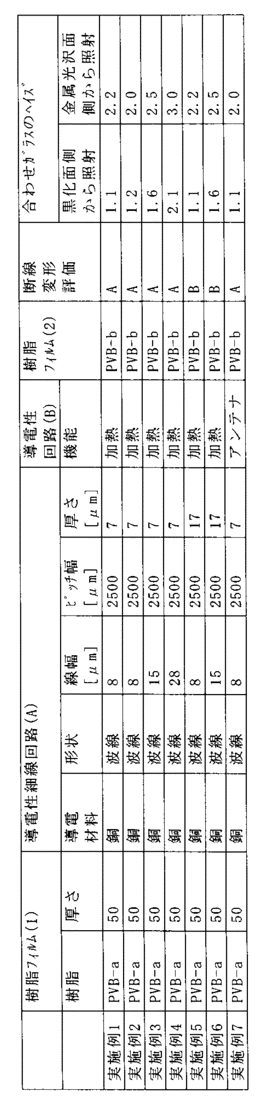
さらに、実施例1~7で得られた合わせガラスは、ヘイズが低く、優れた前方視認性を有することが確認された。
2,6,10,12,16,20,22,28,32,34,38,42,44,48,52…樹脂フィルム
3,7,13,17,23,25,29,35,39,45,49…バスバー
4,8,18,24,26,30,40,46,50…導電細線
9,19,31,41,47…導電性細線回路
5,15,27,37,51…導電性回路
36…ループ状アンテナ
Claims (22)
- 導電性細線回路(A)、樹脂フィルム(1)、及び導電性回路(B)をこの順に有する、回路付きフィルム。
- 前記導電性細線回路(A)及び/又は前記導電性回路(B)が金属箔由来の回路である、請求項1に記載の回路付きフィルム。
- 前記導電性細線回路(A)の厚さが1~30μmである、請求項1又は2に記載の回路付きフィルム。
- 前記導電性回路(B)が加熱機能を有する、請求項1~3のいずれかに記載の回路付きフィルム。
- 前記導電性回路(B)がアンテナ又はセンサーとしての機能を有する、請求項1~3のいずれかに記載の回路付きフィルム。
- 前記樹脂フィルム(1)が、ポリビニルアセタール樹脂、アイオノマー樹脂及びエチレン酢酸ビニル共重合体樹脂からなる群から選ばれる少なくとも1種の樹脂を含有する、請求項1~5のいずれかに記載の回路付きフィルム。
- 前記樹脂フィルム(1)が、樹脂フィルム(1)の質量に対して、50質量%以上のポリビニルアセタール樹脂を含む、請求項1~6のいずれかに記載の回路付きフィルム。
- 前記樹脂フィルム(1)が、樹脂フィルム(1)の質量に対して、0~20質量%の可塑剤を含む、請求項7に記載の回路付きフィルム。
- 質量比1/1のトルエン/エタノール混合液90質量部に対して前記樹脂フィルム(1)10質量部を溶解させた溶液の、ブルックフィールド型(B型)粘度計により20℃、30rpmで測定された粘度が100mPa・s以上である、請求項7又は8に記載の回路付きフィルム。
- 前記樹脂フィルム(1)の厚さが10~350μmである、請求項1~9のいずれかに記載の回路付きフィルム。
- 前記樹脂フィルム(1)が、樹脂フィルム(1)の質量に対して、50質量%以上のポリビニルアセタール樹脂及び10~50質量%の可塑剤を含む、請求項1~6のいずれかに記載の回路付きフィルム。
- 前記樹脂フィルム(1)の厚さが100~1000μmである、請求項11に記載の回路付きフィルム。
- 前記導電性細線回路(A)が銅又は銀からなる、請求項1~12のいずれかに記載の回路付きフィルム。
- 前記導電性細線回路(A)が、全体的又は部分的に線状、格子状、網状又はあみだくじ状である、請求項1~13のいずれかに記載の回路付きフィルム。
- 前記導電性細線回路(A)の線幅が1~30μmである、請求項1~14のいずれかに記載の回路付きフィルム。
- 前記導電性細線回路(A)及び/又は前記導電性回路(B)の、前記樹脂フィルム(1)が存在する面とは反対の面に、少なくとも1つの樹脂フィルム(2)を有する、請求項1~15のいずれかに記載の回路付きフィルム。
- 前記樹脂フィルム(2)が、樹脂フィルム(2)の質量に対して50質量%以上のポリビニルアセタール樹脂及び10~50質量%の可塑剤を含有する、請求項16に記載の回路付きフィルム。
- 少なくとも2枚のガラス板の間に、請求項16又は17に記載の回路付きフィルムを有する合わせガラスであって、樹脂フィルム(1)及び樹脂フィルム(2)の平均可塑剤量が5~50質量%である、合わせガラス。
- 請求項1~15のいずれかに記載の回路付きフィルムの製造方法であって、
樹脂フィルム(1)の一方の面に導電性細線回路(A)を形成し、該樹脂フィルム(1)とは別の樹脂フィルム(1)の一方の面に導電性回路(B)を形成して、樹脂フィルム(1)を有する導電性細線回路(A)及び樹脂フィルム(1)を有する導電性回路(B)を得る工程(i)を含む、回路付きフィルムの製造方法。 - 前記工程(i)で作製した前記樹脂フィルム(1)を有する導電性細線回路(A)の樹脂フィルム(1)と、前記工程(i)で作製した前記樹脂フィルム(1)を有する導電性回路(B)の導電性回路(B)とが接する向きで、両方の回路を積層して、樹脂フィルム(1)、導電性細線回路(A)、樹脂フィルム(1)、及び導電性回路(B)をこの順に有する回路付きフィルムを得る工程(ii-1)を含む、請求項19に記載の製造方法。
- 前記工程(i)で作製した前記樹脂フィルム(1)を有する導電性細線回路(A)の樹脂フィルム(1)と、前記工程(i)で作製した前記樹脂フィルム(1)を有する導電性回路(B)の前記樹脂フィルム(1)とが接する向きで、両方の回路を積層して、導電性細線回路(A)、樹脂フィルム(1)、樹脂フィルム(1)及び導電性回路(B)をこの順に有する回路付きフィルムを得る工程(ii-2)を含む、請求項19に記載の製造方法。
- 少なくとも2枚のガラス板の間に、請求項19~21のいずれかに記載の製造方法で得られた回路付きフィルムを有する、合わせガラスの製造方法。
Priority Applications (2)
| Application Number | Priority Date | Filing Date | Title |
|---|---|---|---|
| KR1020207018501A KR20200104310A (ko) | 2017-12-28 | 2018-12-27 | 회로 부착 필름 |
| JP2019562481A JPWO2019131963A1 (ja) | 2017-12-28 | 2018-12-27 | 回路付きフィルム |
Applications Claiming Priority (2)
| Application Number | Priority Date | Filing Date | Title |
|---|---|---|---|
| JP2017254075 | 2017-12-28 | ||
| JP2017-254075 | 2017-12-28 |
Publications (1)
| Publication Number | Publication Date |
|---|---|
| WO2019131963A1 true WO2019131963A1 (ja) | 2019-07-04 |
Family
ID=67067549
Family Applications (1)
| Application Number | Title | Priority Date | Filing Date |
|---|---|---|---|
| PCT/JP2018/048359 Ceased WO2019131963A1 (ja) | 2017-12-28 | 2018-12-27 | 回路付きフィルム |
Country Status (3)
| Country | Link |
|---|---|
| JP (1) | JPWO2019131963A1 (ja) |
| KR (1) | KR20200104310A (ja) |
| WO (1) | WO2019131963A1 (ja) |
Cited By (4)
| Publication number | Priority date | Publication date | Assignee | Title |
|---|---|---|---|---|
| JPWO2019131948A1 (ja) * | 2017-12-28 | 2021-01-07 | 株式会社クラレ | 回路付きフィルム |
| JP2023501260A (ja) * | 2019-11-18 | 2023-01-18 | エージーシー グラス ユーロップ | 積層グレイジング |
| WO2023145661A1 (ja) * | 2022-01-28 | 2023-08-03 | 三井金属鉱業株式会社 | 発熱体、合わせガラス、及びデフロスタ |
| WO2023145660A1 (ja) * | 2022-01-28 | 2023-08-03 | 三井金属鉱業株式会社 | 発熱体、合わせガラス、及びデフロスタ |
Citations (3)
| Publication number | Priority date | Publication date | Assignee | Title |
|---|---|---|---|---|
| JP2012014945A (ja) * | 2010-06-30 | 2012-01-19 | Fujifilm Corp | 透明導電性フイルム及び発熱ガラスの製造方法 |
| WO2016080406A1 (ja) * | 2014-11-17 | 2016-05-26 | 大日本印刷株式会社 | 発熱板、導電性パターンシート、乗り物、及び、発熱板の製造方法 |
| JP2016539905A (ja) * | 2013-11-29 | 2016-12-22 | クラレイ ユーロップ ゲゼルシャフト ミット ベシュレンクテル ハフツングKuraray Europe GmbH | 埋め込まれた導電性構造体を有する合わせガラス積層体を製造する方法 |
Family Cites Families (1)
| Publication number | Priority date | Publication date | Assignee | Title |
|---|---|---|---|---|
| JP4219790B2 (ja) | 2003-11-14 | 2009-02-04 | 日本板硝子株式会社 | 電熱窓ガラス |
-
2018
- 2018-12-27 KR KR1020207018501A patent/KR20200104310A/ko not_active Withdrawn
- 2018-12-27 WO PCT/JP2018/048359 patent/WO2019131963A1/ja not_active Ceased
- 2018-12-27 JP JP2019562481A patent/JPWO2019131963A1/ja active Pending
Patent Citations (3)
| Publication number | Priority date | Publication date | Assignee | Title |
|---|---|---|---|---|
| JP2012014945A (ja) * | 2010-06-30 | 2012-01-19 | Fujifilm Corp | 透明導電性フイルム及び発熱ガラスの製造方法 |
| JP2016539905A (ja) * | 2013-11-29 | 2016-12-22 | クラレイ ユーロップ ゲゼルシャフト ミット ベシュレンクテル ハフツングKuraray Europe GmbH | 埋め込まれた導電性構造体を有する合わせガラス積層体を製造する方法 |
| WO2016080406A1 (ja) * | 2014-11-17 | 2016-05-26 | 大日本印刷株式会社 | 発熱板、導電性パターンシート、乗り物、及び、発熱板の製造方法 |
Cited By (8)
| Publication number | Priority date | Publication date | Assignee | Title |
|---|---|---|---|---|
| JPWO2019131948A1 (ja) * | 2017-12-28 | 2021-01-07 | 株式会社クラレ | 回路付きフィルム |
| JP7148550B2 (ja) | 2017-12-28 | 2022-10-05 | クラレイ ユーロップ ゲゼルシャフト ミット ベシュレンクテル ハフツング | 回路付きフィルム |
| JP2023501260A (ja) * | 2019-11-18 | 2023-01-18 | エージーシー グラス ユーロップ | 積層グレイジング |
| WO2023145661A1 (ja) * | 2022-01-28 | 2023-08-03 | 三井金属鉱業株式会社 | 発熱体、合わせガラス、及びデフロスタ |
| WO2023145660A1 (ja) * | 2022-01-28 | 2023-08-03 | 三井金属鉱業株式会社 | 発熱体、合わせガラス、及びデフロスタ |
| EP4472351A4 (en) * | 2022-01-28 | 2025-05-07 | Mitsui Mining & Smelting Co., Ltd. | Heat-generating body, laminated glass, and defroster |
| EP4472352A4 (en) * | 2022-01-28 | 2025-05-07 | Mitsui Mining & Smelting Co., Ltd. | HEAT GENERATING BODY, LAMINATED GLASS AND DEFROSTER |
| TWI888789B (zh) * | 2022-01-28 | 2025-07-01 | 日商三井金屬鑛業股份有限公司 | 發熱體、層合玻璃及除霜器 |
Also Published As
| Publication number | Publication date |
|---|---|
| KR20200104310A (ko) | 2020-09-03 |
| JPWO2019131963A1 (ja) | 2021-01-07 |
Similar Documents
| Publication | Publication Date | Title |
|---|---|---|
| JP6457708B1 (ja) | 合わせガラス用のポリビニルアセタール樹脂フィルム | |
| JP6487131B2 (ja) | 合わせガラス用のポリビニルアセタール樹脂フィルム | |
| WO2019131963A1 (ja) | 回路付きフィルム | |
| JP6444407B2 (ja) | 熱線遮蔽特性を有する合わせガラス積層体を製造する方法 | |
| WO2019131928A1 (ja) | 電子部材取付け領域を有する複合フィルム | |
| JP7374888B2 (ja) | ポリビニルアセタール樹脂フィルム | |
| CN110799469B (zh) | 带有基材薄膜的含导电结构体的薄膜的制造方法 | |
| JP2018161889A (ja) | ポリビニルアセタール樹脂層と金属箔に基づく導電性構造体とを有するポリビニルアセタール樹脂フィルム、および前記フィルムを有する合わせガラス | |
| JP7148550B2 (ja) | 回路付きフィルム | |
| WO2019168173A1 (ja) | 可塑剤含有シートが重なってなる多層構造体 | |
| CN112771101B (zh) | 聚乙烯醇缩醛树脂薄膜和包含其的层叠体 | |
| JP7225119B2 (ja) | 積層体及び合わせガラス | |
| JP7830048B2 (ja) | 複合フィルム及びその製造方法 | |
| JP2019150992A (ja) | シートが重なってなる多層構造体 | |
| JP2018188356A (ja) | 窓ガラス用発熱フィルム、および前記フィルムを有する窓ガラス |
Legal Events
| Date | Code | Title | Description |
|---|---|---|---|
| 121 | Ep: the epo has been informed by wipo that ep was designated in this application |
Ref document number: 18896563 Country of ref document: EP Kind code of ref document: A1 |
|
| ENP | Entry into the national phase |
Ref document number: 2019562481 Country of ref document: JP Kind code of ref document: A |
|
| ENP | Entry into the national phase |
Ref document number: 20207018501 Country of ref document: KR Kind code of ref document: A |
|
| NENP | Non-entry into the national phase |
Ref country code: DE |
|
| 122 | Ep: pct application non-entry in european phase |
Ref document number: 18896563 Country of ref document: EP Kind code of ref document: A1 |