WO2019130965A1 - 出力回路 - Google Patents
出力回路 Download PDFInfo
- Publication number
- WO2019130965A1 WO2019130965A1 PCT/JP2018/043800 JP2018043800W WO2019130965A1 WO 2019130965 A1 WO2019130965 A1 WO 2019130965A1 JP 2018043800 W JP2018043800 W JP 2018043800W WO 2019130965 A1 WO2019130965 A1 WO 2019130965A1
- Authority
- WO
- WIPO (PCT)
- Prior art keywords
- wiring
- output
- gate
- vnw
- transistor
- Prior art date
- Legal status (The legal status is an assumption and is not a legal conclusion. Google has not performed a legal analysis and makes no representation as to the accuracy of the status listed.)
- Ceased
Links
Images










Classifications
-
- H—ELECTRICITY
- H10—SEMICONDUCTOR DEVICES; ELECTRIC SOLID-STATE DEVICES NOT OTHERWISE PROVIDED FOR
- H10D—INORGANIC ELECTRIC SEMICONDUCTOR DEVICES
- H10D84/00—Integrated devices formed in or on semiconductor substrates that comprise only semiconducting layers, e.g. on Si wafers or on GaAs-on-Si wafers
- H10D84/01—Manufacture or treatment
- H10D84/0123—Integrating together multiple components covered by H10D12/00 or H10D30/00, e.g. integrating multiple IGBTs
- H10D84/0126—Integrating together multiple components covered by H10D12/00 or H10D30/00, e.g. integrating multiple IGBTs the components including insulated gates, e.g. IGFETs
- H10D84/016—Integrating together multiple components covered by H10D12/00 or H10D30/00, e.g. integrating multiple IGBTs the components including insulated gates, e.g. IGFETs the components including vertical IGFETs
-
- B—PERFORMING OPERATIONS; TRANSPORTING
- B82—NANOTECHNOLOGY
- B82Y—SPECIFIC USES OR APPLICATIONS OF NANOSTRUCTURES; MEASUREMENT OR ANALYSIS OF NANOSTRUCTURES; MANUFACTURE OR TREATMENT OF NANOSTRUCTURES
- B82Y10/00—Nanotechnology for information processing, storage or transmission, e.g. quantum computing or single electron logic
-
- H—ELECTRICITY
- H10—SEMICONDUCTOR DEVICES; ELECTRIC SOLID-STATE DEVICES NOT OTHERWISE PROVIDED FOR
- H10D—INORGANIC ELECTRIC SEMICONDUCTOR DEVICES
- H10D30/00—Field-effect transistors [FET]
- H10D30/60—Insulated-gate field-effect transistors [IGFET]
- H10D30/63—Vertical IGFETs
-
- H—ELECTRICITY
- H10—SEMICONDUCTOR DEVICES; ELECTRIC SOLID-STATE DEVICES NOT OTHERWISE PROVIDED FOR
- H10D—INORGANIC ELECTRIC SEMICONDUCTOR DEVICES
- H10D62/00—Semiconductor bodies, or regions thereof, of devices having potential barriers
- H10D62/10—Shapes, relative sizes or dispositions of the regions of the semiconductor bodies; Shapes of the semiconductor bodies
- H10D62/117—Shapes of semiconductor bodies
- H10D62/118—Nanostructure semiconductor bodies
- H10D62/119—Nanowire, nanosheet or nanotube semiconductor bodies
- H10D62/122—Nanowire, nanosheet or nanotube semiconductor bodies oriented at angles to substrates, e.g. perpendicular to substrates
-
- H—ELECTRICITY
- H10—SEMICONDUCTOR DEVICES; ELECTRIC SOLID-STATE DEVICES NOT OTHERWISE PROVIDED FOR
- H10D—INORGANIC ELECTRIC SEMICONDUCTOR DEVICES
- H10D64/00—Electrodes of devices having potential barriers
- H10D64/20—Electrodes characterised by their shapes, relative sizes or dispositions
- H10D64/27—Electrodes not carrying the current to be rectified, amplified, oscillated or switched, e.g. gates
- H10D64/311—Gate electrodes for field-effect devices
-
- H—ELECTRICITY
- H10—SEMICONDUCTOR DEVICES; ELECTRIC SOLID-STATE DEVICES NOT OTHERWISE PROVIDED FOR
- H10D—INORGANIC ELECTRIC SEMICONDUCTOR DEVICES
- H10D84/00—Integrated devices formed in or on semiconductor substrates that comprise only semiconducting layers, e.g. on Si wafers or on GaAs-on-Si wafers
- H10D84/01—Manufacture or treatment
- H10D84/0123—Integrating together multiple components covered by H10D12/00 or H10D30/00, e.g. integrating multiple IGBTs
- H10D84/0126—Integrating together multiple components covered by H10D12/00 or H10D30/00, e.g. integrating multiple IGBTs the components including insulated gates, e.g. IGFETs
- H10D84/0165—Integrating together multiple components covered by H10D12/00 or H10D30/00, e.g. integrating multiple IGBTs the components including insulated gates, e.g. IGFETs the components including complementary IGFETs, e.g. CMOS devices
- H10D84/0186—Manufacturing their interconnections or electrodes, e.g. source or drain electrodes
-
- H—ELECTRICITY
- H10—SEMICONDUCTOR DEVICES; ELECTRIC SOLID-STATE DEVICES NOT OTHERWISE PROVIDED FOR
- H10D—INORGANIC ELECTRIC SEMICONDUCTOR DEVICES
- H10D84/00—Integrated devices formed in or on semiconductor substrates that comprise only semiconducting layers, e.g. on Si wafers or on GaAs-on-Si wafers
- H10D84/01—Manufacture or treatment
- H10D84/0123—Integrating together multiple components covered by H10D12/00 or H10D30/00, e.g. integrating multiple IGBTs
- H10D84/0126—Integrating together multiple components covered by H10D12/00 or H10D30/00, e.g. integrating multiple IGBTs the components including insulated gates, e.g. IGFETs
- H10D84/0165—Integrating together multiple components covered by H10D12/00 or H10D30/00, e.g. integrating multiple IGBTs the components including insulated gates, e.g. IGFETs the components including complementary IGFETs, e.g. CMOS devices
- H10D84/0195—Integrating together multiple components covered by H10D12/00 or H10D30/00, e.g. integrating multiple IGBTs the components including insulated gates, e.g. IGFETs the components including complementary IGFETs, e.g. CMOS devices the components including vertical IGFETs
-
- H—ELECTRICITY
- H10—SEMICONDUCTOR DEVICES; ELECTRIC SOLID-STATE DEVICES NOT OTHERWISE PROVIDED FOR
- H10D—INORGANIC ELECTRIC SEMICONDUCTOR DEVICES
- H10D84/00—Integrated devices formed in or on semiconductor substrates that comprise only semiconducting layers, e.g. on Si wafers or on GaAs-on-Si wafers
- H10D84/01—Manufacture or treatment
- H10D84/02—Manufacture or treatment characterised by using material-based technologies
- H10D84/03—Manufacture or treatment characterised by using material-based technologies using Group IV technology, e.g. silicon technology or silicon-carbide [SiC] technology
- H10D84/038—Manufacture or treatment characterised by using material-based technologies using Group IV technology, e.g. silicon technology or silicon-carbide [SiC] technology using silicon technology, e.g. SiGe
-
- H—ELECTRICITY
- H10—SEMICONDUCTOR DEVICES; ELECTRIC SOLID-STATE DEVICES NOT OTHERWISE PROVIDED FOR
- H10D—INORGANIC ELECTRIC SEMICONDUCTOR DEVICES
- H10D84/00—Integrated devices formed in or on semiconductor substrates that comprise only semiconducting layers, e.g. on Si wafers or on GaAs-on-Si wafers
- H10D84/80—Integrated devices formed in or on semiconductor substrates that comprise only semiconducting layers, e.g. on Si wafers or on GaAs-on-Si wafers characterised by the integration of at least one component covered by groups H10D12/00 or H10D30/00, e.g. integration of IGFETs
- H10D84/82—Integrated devices formed in or on semiconductor substrates that comprise only semiconducting layers, e.g. on Si wafers or on GaAs-on-Si wafers characterised by the integration of at least one component covered by groups H10D12/00 or H10D30/00, e.g. integration of IGFETs of only field-effect components
- H10D84/83—Integrated devices formed in or on semiconductor substrates that comprise only semiconducting layers, e.g. on Si wafers or on GaAs-on-Si wafers characterised by the integration of at least one component covered by groups H10D12/00 or H10D30/00, e.g. integration of IGFETs of only field-effect components of only insulated-gate FETs [IGFET]
- H10D84/85—Complementary IGFETs, e.g. CMOS
-
- H—ELECTRICITY
- H10—SEMICONDUCTOR DEVICES; ELECTRIC SOLID-STATE DEVICES NOT OTHERWISE PROVIDED FOR
- H10D—INORGANIC ELECTRIC SEMICONDUCTOR DEVICES
- H10D89/00—Aspects of integrated devices not covered by groups H10D84/00 - H10D88/00
- H10D89/10—Integrated device layouts
-
- H—ELECTRICITY
- H10—SEMICONDUCTOR DEVICES; ELECTRIC SOLID-STATE DEVICES NOT OTHERWISE PROVIDED FOR
- H10P—GENERIC PROCESSES OR APPARATUS FOR THE MANUFACTURE OR TREATMENT OF DEVICES COVERED BY CLASS H10
- H10P14/00—Formation of materials, e.g. in the shape of layers or pillars
- H10P14/20—Formation of materials, e.g. in the shape of layers or pillars of semiconductor materials
- H10P14/34—Deposited materials, e.g. layers
- H10P14/3451—Structure
- H10P14/3452—Microstructure
- H10P14/3462—Nanowires
-
- H—ELECTRICITY
- H10—SEMICONDUCTOR DEVICES; ELECTRIC SOLID-STATE DEVICES NOT OTHERWISE PROVIDED FOR
- H10D—INORGANIC ELECTRIC SEMICONDUCTOR DEVICES
- H10D30/00—Field-effect transistors [FET]
- H10D30/01—Manufacture or treatment
- H10D30/014—Manufacture or treatment of FETs having zero-dimensional [0D] or one-dimensional [1D] channels, e.g. quantum wire FETs, single-electron transistors [SET] or Coulomb blockade transistors
-
- H—ELECTRICITY
- H10—SEMICONDUCTOR DEVICES; ELECTRIC SOLID-STATE DEVICES NOT OTHERWISE PROVIDED FOR
- H10D—INORGANIC ELECTRIC SEMICONDUCTOR DEVICES
- H10D30/00—Field-effect transistors [FET]
- H10D30/40—FETs having zero-dimensional [0D], one-dimensional [1D] or two-dimensional [2D] charge carrier gas channels
- H10D30/43—FETs having zero-dimensional [0D], one-dimensional [1D] or two-dimensional [2D] charge carrier gas channels having one-dimensional [1D] charge carrier gas channels, e.g. quantum wire FETs or transistors having 1D quantum-confined channels
-
- H—ELECTRICITY
- H10—SEMICONDUCTOR DEVICES; ELECTRIC SOLID-STATE DEVICES NOT OTHERWISE PROVIDED FOR
- H10D—INORGANIC ELECTRIC SEMICONDUCTOR DEVICES
- H10D30/00—Field-effect transistors [FET]
- H10D30/60—Insulated-gate field-effect transistors [IGFET]
- H10D30/67—Thin-film transistors [TFT]
- H10D30/6728—Vertical TFTs
-
- H—ELECTRICITY
- H10—SEMICONDUCTOR DEVICES; ELECTRIC SOLID-STATE DEVICES NOT OTHERWISE PROVIDED FOR
- H10D—INORGANIC ELECTRIC SEMICONDUCTOR DEVICES
- H10D62/00—Semiconductor bodies, or regions thereof, of devices having potential barriers
- H10D62/10—Shapes, relative sizes or dispositions of the regions of the semiconductor bodies; Shapes of the semiconductor bodies
- H10D62/13—Semiconductor regions connected to electrodes carrying current to be rectified, amplified or switched, e.g. source or drain regions
- H10D62/149—Source or drain regions of field-effect devices
- H10D62/151—Source or drain regions of field-effect devices of IGFETs
-
- H—ELECTRICITY
- H10—SEMICONDUCTOR DEVICES; ELECTRIC SOLID-STATE DEVICES NOT OTHERWISE PROVIDED FOR
- H10D—INORGANIC ELECTRIC SEMICONDUCTOR DEVICES
- H10D64/00—Electrodes of devices having potential barriers
- H10D64/20—Electrodes characterised by their shapes, relative sizes or dispositions
- H10D64/23—Electrodes carrying the current to be rectified, amplified, oscillated or switched, e.g. sources, drains, anodes or cathodes
- H10D64/251—Source or drain electrodes for field-effect devices
- H10D64/252—Source or drain electrodes for field-effect devices for vertical or pseudo-vertical devices
Definitions
- the transistor which is a basic component of LSI, has achieved improvement in integration, reduction in operating voltage, and improvement in operating speed by reducing the gate length (scaling).
- the off current due to excessive scaling and the significant increase in power consumption due to it have become problems.
- a three-dimensional structure transistor in which the transistor structure is changed from the conventional flat type to a three-dimensional type is actively studied.
- a vertical nanowire FET hereinafter, referred to as a VNW FET as appropriate
- an output circuit for outputting a signal from a semiconductor integrated circuit is provided between a first power supply and an output signal line, and of a first conductivity type receiving a first output control signal at a gate.
- a plurality of first VNW FETs including a first transistor, the first transistors being arranged in an array in a first direction and a second direction perpendicular to the first direction, the plurality of first VNWs The top of the FET is connected to the output signal line, the first power supply voltage is given from the first power supply at the bottom, and the first output control signal is given to the gate.
- an output circuit for outputting a signal from a semiconductor integrated circuit includes first and second transistors of a first conductivity type provided in series between a first power supply and an output signal line.
- the first transistor receives a first output control signal at its gate
- the second transistor receives a second output control signal at its gate
- the first transistor has a first direction and the first direction.
- the semiconductor integrated circuit device includes a plurality of IO cells, and at least a part of the IO cells includes a so-called vertical nanowire FET (VNW FET).
- VNW FET vertical nanowire FET
- the VNW FET 510 is arranged in the vertical direction (perpendicular to the substrate surface) between the bottom electrode 511 serving as the source / drain electrode, the top electrode 512 serving as the source / drain electrode, and the bottom electrode 511 and the top electrode 512. And the formed nanowire 513.
- the bottom electrode 511 and the top electrode 512 are doped with N conductivity.
- At least a part of the nanowire 513 is a channel region.
- a gate insulating film 515 is formed around the nanowire 513, and a gate electrode 514 is formed around it. Note that the gate electrode 514 may surround the entire periphery of the nanowire 513 or may surround only a part of the periphery of the nanowire 513. When the gate electrode 514 surrounds only a part of the periphery of the nanowire 513, the gate insulating film 515 may be formed only in the portion where the gate electrode 514 surrounds the nanowire 513.
- the bottom electrode 511 is connected to a bottom region 516 formed to extend along the upper surface of the semiconductor substrate 501.
- Bottom region 516 is also doped with N conductivity type.
- a silicide region 517 is formed on the surface of the bottom region 516.
- sidewalls 518 are formed around the top electrode 512.
- a silicide region 519 is formed on the top electrode 512. However, the sidewall 518 and the silicide region 519 may not be formed.
- the material of the silicide regions 519 and 529 provided on the top electrodes 512 and 522 may be NiSi, CoSi, MoSi, WSi, PtSi, TiSi, or a combination of these, or the like.
- a metal such as W, Cu, Al, an alloy such as TiN, TaN, an impurity-implanted semiconductor, or the like, or a combination thereof may be used.
- Examples of the material of the side walls 518 and 528 include SiN, SiON, SiC, SiCN, and SiOCN.
- Examples of the material of the contact 532 include Ti, TiN, Ta, TaN and the like. In addition, there are Cu, Cu-arroy, W, Ag, Au, Ni, Al and the like. Alternatively, Co or Ru may be used.
- FIG. 23 shows an example of the basic structure of the VNW FET and shows an example of the structure using local wiring.
- the local interconnection 534 is formed between the metal interconnection layer M1 and the top electrode 512 of the VNW FET 510 and the top electrode 522 of the VNW FET 520.
- Bottom regions 516 and 526 and gate interconnection 531 are connected to interconnection 542 formed in metal interconnection layer M1 via contact 533, local interconnection 534 and contact 541, respectively.
- the silicide regions 519 and 529 are connected to the wiring 542 formed in the metal wiring layer M1 through the local wiring 534 and the contact 541, respectively.
- VNW FET the bottom electrode, the top electrode and the gate electrode of the VNW FET will be referred to simply as the bottom, top and gate as appropriate.
- VNW a unit configuration consisting of vertical nanowires, top, bottom and gate constitutes one VNW FET by one or more
- VNW VNW FET
- FIG. 1 is a plan view schematically showing the entire configuration of a semiconductor integrated circuit device (semiconductor chip) according to the embodiment.
- the semiconductor integrated circuit device 1 shown in FIG. 1 includes a core region 2 in which an internal core circuit is formed, and an IO region 3 provided around the core region 2 and in which an interface circuit (IO circuit) is formed.
- an IO cell array 5 is provided to surround the core region 2 in the peripheral portion of the semiconductor integrated circuit device 1.
- a plurality of IO cells 10 constituting an interface circuit are arranged in the IO cell row 5.
- the IO cell 10 is a signal IO cell for inputting, outputting or inputting / outputting a signal, a power supply IO cell for supplying a ground potential (power supply voltage VSS), mainly to the IO area 3 (power supply voltage Power supply IO cells for supplying VDDIO).
- VSSIO power supply voltage
- VDDIO is 3.3V.
- the IO cell 10A for signal input / output is disposed on the upper side of the core region 2 in the drawing
- the IO cell 10B for signal input / output is disposed on the left side of the core region 2 in the drawing.
- power supply wirings 6 and 7 extending in the direction in which the IO cells 10 are arranged are provided.
- the power supply wirings 6 and 7 are formed in a ring shape on the periphery of the semiconductor integrated circuit device 1 (also referred to as a ring power supply wiring).
- the power supply line 6 supplies VDDIO
- the power supply line 7 supplies VSS.
- each of the power supply wirings 6 and 7 is illustrated as a single wiring in FIG. 1, actually, the power supply wirings 6 and 7 may each be configured by a plurality of wirings. .
- the semiconductor integrated circuit device 1 is provided with a plurality of external connection pads.
- the N conductivity type output transistor section 103 is provided under the power supply wiring 7
- the P conductivity type output transistor section 104 is provided under the power supply wiring 6.
- the N conductivity type output transistor unit 103 and the P conductivity type output transistor unit 104 are provided in the IO cell 10B at a position from the chip outer side.
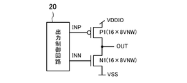
- the layout structure of two transistors P1 and N1 which comprise the output circuit of FIG. 3 is demonstrated.
- the transistor N1 is configured in the N conductivity type output transistor unit 101
- the transistor P1 is configured in the P conductivity type output transistor unit 102.
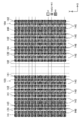
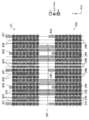
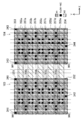
- FIGS. 5 to 7 are plan views according to layers
- FIG. 5 shows the VNW FET and the layers therebelow
- FIG. 6 shows the local and M1 lines above the VNW FET
- FIG. 7 shows the M1 and M2 lines.
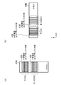
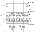
- FIG. 8 is a cross-sectional view in the lateral direction of a plan view of FIG.
- FIG. 4 is a cross section of line X1-X1 ', (b) is a cross section of line X2-X2', and (c) is a line X3-X3 ' It is a cross section.
- 9 is a cross-sectional view of FIG. 4 in the vertical direction in plan view, where (a) is the cross section of line Y1-Y1 ', (b) is the cross section of line Y2-Y2', and (c) is the line Y3-Y3 ' It is a cross section.
- dotted lines running in the vertical and horizontal directions in the plan view of FIG. 4 and the like and dotted lines running in the vertical direction in the cross-sectional view of FIG. 8 and the like indicate grids used to arrange components during design.
- the grids are arranged at equal intervals in the X direction and at equal intervals in the Y direction.
- the grid intervals may be the same or different in the X direction and the Y direction.
- the grid spacing may be different for each layer.
- the grid of the VNW FET and the grid of the M1 wire may be arranged at different intervals.
- the parts do not necessarily have to be arranged on the grid. However, from the viewpoint of suppressing manufacturing variations, it is preferable to place the components on the grid.
- the device structure according to the present embodiment is premised on the structure of FIG. However, the structure shown in FIG. 22 or 23 (b) or another device structure may be assumed. The same applies to the following embodiments. Further, in order to make the drawing easy to understand, illustration is omitted for the well, STI, each insulating film, the silicide layer on the bottom, the silicide layer on the top, and the sidewall on the top. The same applies to the following figures.
- the upper side of the drawing corresponds to the N conductivity type output transistor section 101, and the transistor N1 in the circuit of FIG. 3 is realized. Further, the lower side of the drawing corresponds to the P conductivity type output transistor section 102, and implements the transistor P1 in the circuit of FIG.
- N-type VNWs V1 are formed in an array of 16 rows in the X direction and 8 rows in the Y direction, for a total of 128 rows.
- the transistor N1 is realized by the 128 N-type VNWs V1.
- the bottom region 11 is formed over the substantially entire surface of the N-conductive output transistor unit 101, and the bottom of the 128 VNWs V 1 is connected to the bottom region 11.
- VNW V1 is spaced apart in every other two rows in the X direction.
- the group of VNW V1 in every two columns is gn1 to gn8.
- the gates VNW V1 adjacent in the X direction are connected to each other.
- the gate line 21 is drawn from the group gn1 to the left side in the drawing, and the gate line 22 is drawn from the group gn8 to the right side in the drawing.
- four VNWs V 1 adjacent in the X direction are connected by the gate wiring 23.
- the gate wiring 23 is a gate wiring drawn out from the group gn2 to the right side in the drawing and a gate wiring drawn out from the group gn3 to the left side in the drawing.
- the four VNWs V1 adjacent in the X direction are connected by the gate wiring 23, and in the groups gn6 and gn7, the four VNWs V1 adjacent in the X direction are the gate wiring 23 It is connected.
- Vias 27a are formed in the gate interconnections 21, 22, and 23 for connection to the upper local interconnections. Further, in the bottom region 11, vias 27b for connecting to the local interconnections in the upper layer thereof are connected between the groups gn1 and gn2, between the groups gn3 and gn4, between the groups gn5 and gn6, and between the groups gn7 and gn8. It is formed so as to line up in the Y direction in between.
- P type VNWs V2 are formed in an array of 16 rows in the X direction and 8 rows in the Y direction, for a total of 128 pieces.
- the transistor P1 is realized by the 128 P-type VNWs V2.
- a bottom region 12 is formed over the substantially entire surface of the P-conductive output transistor portion 102, and the bottom of the 128 VNWs V 2 is connected to the bottom region 12.
- VNW V2 is spaced apart in every other two rows in the X direction.
- the group of VNW V2 in every two rows is gp1 to gp8.
- the gates VNW V2 adjacent in the X direction are connected to each other.
- a gate line 24 is drawn from the group gp1 to the left side in the drawing, and a gate line 25 is drawn from the group gp8 to the right side in the drawing.
- four VNWs V 2 adjacent in the X direction are connected by the gate line 26.
- the gate interconnection 26 is a gate interconnection drawn from the group gp2 to the right in the drawing, and a gate interconnection drawn from the group gp3 to the left in the drawing.
- the groups gp4 and gp5 four VNWs V2 adjacent in the X direction are connected by the gate wiring 26.
- the groups gp6 and gp7 four VNWs V2 adjacent in the X direction are connected by the gate wiring 26. It is connected.
- Vias 28a are formed in the gate interconnections 24, 25 and 26 for connection to the local interconnections thereabove. Also, in the bottom region 12, vias 28b for connecting to the local interconnections in the upper layer are formed between the groups gp1 and gp2, between the groups gp3 and gp4, between the groups gp5 and gp6, and in the groups gp7 and gp8. It is formed so as to line up in the Y direction in between.
- M2 interconnections 51, 52, 53, 56a to 56d and 57a to 57d extending in the X direction are formed.
- the M2 wire 51 supplies an output control signal INN.
- the M2 line 52 supplies an output control signal INP.
- the M2 wiring 53 is a signal line that outputs the output signal OUT, and corresponds to the output signal line in the present disclosure.
- the M2 wirings 56a to 56d are wirings for supplying the power supply voltage VSS, and correspond to the power supply wiring 7.
- the M2 wires 57 a to 57 d are wires for supplying the power supply voltage VDDIO, and correspond to the power supply wire 6.
- M1 interconnections 41, 42, 43, 44 and 45 extending in the Y direction are formed.
- the M1 wiring 41 is disposed in the N conductivity type output transistor unit 101, and is connected to the M2 wiring 51 that supplies the output control signal INN through a via.
- the M1 wire 42 is disposed in the P conductivity type output transistor unit 102, and is connected to the M2 wire 52 for supplying the output control signal INP via a via.
- the M1 wire 43 is disposed in the N conductivity type output transistor unit 101, and is connected to the M2 wires 56a to 56d for supplying the power supply voltage VSS via vias.
- the M1 interconnection 44 is disposed in the P conductivity type output transistor unit 102, and is connected to the M2 interconnections 57a to 57d for supplying the power supply voltage VDDIO through vias.
- the M1 wire 45 is disposed across the N conductivity type output transistor portion 101 and the P conductivity type output transistor portion 102.
- the M1 wires 45 are arranged in pairs, and arranged on the groups gn1 to gn8 of VNW V1 and the groups gp1 to gp8 of VNW V2 facing each other in the Y direction. .
- the M1 wiring 45 is connected to the top of each VNW V1 via the local wiring 31 and is connected to the top of each VNW V2 via the local wiring 32 and M2 wiring 53 that outputs the output signal OUT And vias are connected.
- the 128 VNWs V1 formed in the N-conductivity type output transistor portion 101 have M2 wire 53 whose top outputs the output signal OUT via the local wire 31 and M1 wire 45. It is connected.
- the bottom is connected to the M2 wirings 56a to 56d for supplying the power supply voltage VSS through the bottom region 11, the via 27b, and the M1 wiring 43.
- the gate is connected to the M2 wiring 51 for supplying the output control signal INN through the gate wirings 21, 22 and 23, the via 27 a and the M1 wiring 41. Therefore, the transistor N1 in the circuit diagram of FIG. 3 is realized by the 128 VNWs V1 formed in the N conductivity type output transistor section 101.
- the 128 VNWs V2 formed in the P conductivity type output transistor portion 102 are connected at the top to the M2 wire 53 for outputting the output signal OUT via the local wire 32 and the M1 wire 45.
- the bottom is connected to the M2 wires 57a to 57d for supplying the power supply voltage VDDIO through the bottom region 12, the via 28b, and the M1 wire 44.
- the gate is connected to the M2 wiring 52 supplying the output control signal INP via the gate wirings 24, 25, 26, the via 28a, and the M1 wiring 42. Therefore, the transistor P1 in the circuit diagram of FIG. 3 is realized by the 128 VNWs V2 formed in the P conductivity type output transistor section 102.
- an output circuit that allows a large current to flow through the output pad can be configured using a VNW FET.
- gate interconnections 21 to 26 are formed to extend in the X direction, and have the same interconnection width.
- the local interconnections 31 and 32 are formed to extend in the X direction, and have the same interconnection width.
- the M1 wirings 41 to 45 are formed to extend in the Y direction, and have the same wiring width.
- the gate wirings 21 to 26, the local wirings 31 and 32, and the M1 wirings 41 to 45 appear to have the same wiring width, but have different wiring layers with the same wiring width. There is no need, and if the direction and width of the wiring in one wiring layer are the same, manufacture is facilitated and manufacturing accuracy is improved.
- the M1 wire 45 connected to the top of the VNW V1 in the N-conductive output transistor unit 101 has a larger area than the M1 wire 43 in plan view.
- the M1 wire 45 connected to the top of the VNW V2 has a larger area than the M1 wire 44.
- the resistance value to the M2 wiring 53 which outputs the output signal OUT can be reduced.
- the resistance value to the output signal line is reduced compared to the case where the M2 wiring 53 is connected to the bottoms of the VNWs V1 and V2.
- the supply of the output control signal INN to the gate and the supply of the power supply voltage VSS to the bottom are performed from both sides in the X direction.
- the output control signal INN is applied to the gate from the left side of the drawing through the via 27a
- the power supply voltage VSS is applied from the right side to the bottom of the drawing through the via 27b.
- the supply of the output control signal INP to the gate and the supply of the power supply voltage VDDIO to the bottom are performed from both sides in the X direction.
- the output control signal INP is applied to the gate from the left side of the drawing through the via 28a, and the power supply voltage VSS is applied from the right side to the bottom of the drawing through the via 28b.
- the size in the Y direction can be reduced, and a reduction in area can be realized.
- the vias 27a for supplying the output control signal INN may be arranged in two or more rows.
- the vias 28a for supplying the output control signal INP may be arranged side by side in two or more rows.
- the vias 27b for supplying the power supply voltage VSS to the bottom region 11 may be arranged in two or more rows.
- the vias 28b for supplying the power supply voltage VDDIO to the bottom region 12 may be arranged side by side in two or more columns.
- the bottom region 11 is integrally formed in the N conductivity type output transistor portion 101, and the bottom region 12 is integrally formed in the P conductivity type output transistor portion 102.
- the bottom regions 11 and 12 may be formed separately.
- the bottom region 11 may be divided into groups gn1 to gn8.
- the power supply can be stabilized by integrally forming the bottom regions 11 and 12.
- the N conductivity type output transistor section 103 constitutes the transistor N1
- the P conductivity type output transistor section 104 constitutes the transistor P1.
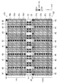
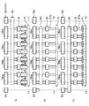
- FIGS. 10 to 13 are plan views according to layers showing examples of the layout structure of the transistors P1 and N1 according to the present embodiment. Specifically, FIG. 10 shows the VNW FET and layers therebelow, FIG. 11 shows the local wiring and M1 wiring above the VNW FET, FIG. 12 shows the M1 and M2 wiring, and FIG. 13 shows the M2 and M2 wiring. The M3 wiring is shown. The overall plan view and the cross-sectional view are omitted here because they can be easily inferred from the first embodiment.
- the left side of the drawing corresponds to the N conductivity type output transistor section 103, and implements the transistor N1 in the circuit of FIG.
- the right side of the drawing corresponds to the P conductivity type output transistor section 104, and implements the transistor P1 in the circuit of FIG.
- N-type VNWs V1 are formed in an array of 128 columns in eight rows in the X direction and sixteen rows in the Y direction.
- the transistor N1 is realized by the 128 N-type VNWs V1.
- a bottom region 111 is formed over substantially the entire surface of the N conductivity type output transistor portion 103, and the bottom of the 128 VNWs V 1 is connected to the bottom region 111.
- VNW V1 is spaced apart in every other two rows in the X direction.
- the group of VNW V1 in every two columns is gn1 to gn4.
- the gates VNW V1 adjacent in the X direction are connected to each other.
- the gate line 121 is drawn out from the group gn1 to the left side of the drawing
- the gate line 122 is drawn out from the group gn4 to the right side in the drawing.
- the groups gn2 and gn3 four VNWs V1 adjacent in the X direction are connected by the gate wiring 123. That is, the gate wiring 123 is a gate wiring drawn from the group gn2 to the right in the drawing and a gate wiring drawn from the group gn3 to the left in the drawing.
- vias 127a for connecting to the local wirings in the upper layer are formed in the gate wirings 121, 122, 123. Also, in the bottom region 111, vias 127b for connecting to the local interconnections in the upper layer are formed in the Y direction between the groups gn1 and gn2 and between the groups gn3 and gn4. .
- P-type VNWs V2 are formed in an array of 128 rows in eight rows in the X direction and 16 rows in the Y direction.
- the transistor P1 is realized by the 128 P-type VNWs V2.
- a bottom region 112 is formed over substantially the entire surface of the P-conductive output transistor portion 104, and the bottom of the 128 VNWs V 2 is connected to the bottom region 112.
- VNW V2 is spaced apart in every other two rows in the X direction.
- the group of VNW V2 in every two rows is gp1 to gp4.
- the gates VNW V2 adjacent in the X direction are connected to each other.
- a gate line 124 is drawn out of the group gp1 to the left side of the drawing, and a gate line 125 is drawn out of the group gp4 to the right side of the drawing.
- the groups gp 2 and gp 3 four VNWs V 2 adjacent in the X direction are connected by the gate wiring 126. That is, the gate interconnection 126 is a gate interconnection drawn from the group gp2 to the right in the drawing and a gate interconnection drawn from the group gp3 to the left in the drawing.
- Vias 128a are formed in the gate interconnections 124, 125, 126 for connection to the local interconnections thereabove. Also, in the bottom region 112, the vias 128b for connecting to the local interconnections in the upper layer are formed in the Y direction between the groups gp1 and gp2 and between the groups gp3 and gp4. .
- M3 wirings 161 and 162a to 162d and 163a to 163d extending in the Y direction are formed.
- the M3 wiring 161 outputs the output signal OUT, and corresponds to the output signal line in the present disclosure.
- the M3 wirings 162a to 162d are wirings for supplying the power supply voltage VSS, and correspond to the power supply wiring 7.
- the M3 wires 163 a to 163 d are wires for supplying the power supply voltage VDDIO, and correspond to the power supply wire 6.
- M2 interconnections 151, 152, 153a to 153e, 154a to 154e, 155a to 155e extending in the X direction are formed.
- the M2 wiring 151 supplies an output control signal INN.
- the M2 line 152 supplies an output control signal INP.
- the M2 wires 153a to 153e are connected to the M3 wire 161 outputting the output signal OUT via a via.
- the M2 wires 154a to 154e are connected to M3 wires 162a to 162d for supplying the power supply voltage VSS via vias.
- the M2 wires 155a to 155e are connected to M3 wires 163a to 163d for supplying the power supply voltage VDDIO through vias.
- M1 interconnections 141, 142, 143, 144, 145, 146 extending in the Y direction are formed in the M1 interconnection layer.
- the M1 wiring 141 is disposed in the N conductivity type output transistor unit 103, and is connected to the M2 wiring 151 that supplies the output control signal INN via a via.
- the M1 wiring 142 is disposed in the P conductivity type output transistor unit 104, and is connected to the M2 wiring 152 supplying the output control signal INP via a via.
- the M1 wire 143 is disposed in the N conductivity type output transistor unit 103, and is connected to the M2 wires 154a to 154e through a via.
- the M1 wire 144 is disposed in the P conductivity type output transistor unit 104, and is connected to the M2 wires 155a to 155e via a via.
- the M1 interconnections 145 are disposed in the N conductivity type output transistor unit 103, and are arranged in pairs, respectively, on the groups gn1 to gn4 of VNW V1.
- the M1 wiring 145 is connected to the top of each VNW V1 via the local wiring 131, and is connected to the M2 wirings 153a to 153e via a via.
- the M1 wire 146 is disposed in the P-conductivity type output transistor unit 104, and is disposed in pairs by two, and disposed on the groups gp1 to gp4 of VNW V2. .
- the M1 wiring 146 is connected to the top of each VNW V1 via the local wiring 132, and is connected to the M2 wirings 153a to 153e via a via.
- the 128 VNWs V1 formed in the N conductivity type output transistor portion 103 have the output signal OUT at the top through the local wiring 131, the M1 wiring 145, and the M2 wirings 153a to 153e. It is connected to the M3 wiring 161 to be output.
- the bottom is connected to the M3 wirings 162a to 162d for supplying the power supply voltage VSS via the bottom region 111, the via 127b, the M1 wiring 143, and the M2 wirings 154a to 154e.
- the gate is connected to the M2 wiring 151 which supplies the output control signal INN via the gate wirings 121, 122, 123, the via 127a, and the M1 wiring 141. Therefore, the transistor N1 in the circuit diagram of FIG. 3 is realized by the 128 VNWs V1 formed in the N conductivity type output transistor section 103.
- the 128 VNWs V2 formed in the P conductivity type output transistor portion 104 have an M3 wire 161 whose top outputs an output signal OUT via the local wire 132, the M1 wire 146, and the M2 wires 153a to 153e. It is connected. The bottom is connected to the M3 wirings 163a to 163d for supplying the power supply voltage VDDIO via the bottom region 112, the via 128b, the M1 wiring 144, and the M2 wirings 155a to 155e. Further, the gate is connected to the M2 wiring 152 supplying the output control signal INP via the gate wirings 124, 125, 126, the via 128a, and the M1 wiring 142. Therefore, the transistor P1 in the circuit diagram of FIG. 3 is realized by the 128 VNWs V2 formed in the P conductivity type output transistor unit 104.
- an output circuit that allows a large current to flow through the output pad can be configured using a VNW FET.
- gate interconnections 121 to 126 are formed to extend in the X direction, and have the same interconnection width.
- the local interconnections 131 and 132 are formed to extend in the X direction, and have the same interconnection width.
- the M1 wires 141 to 146 are formed to extend in the Y direction, and have the same wire width.
- the gate wirings 121 to 126, the local wirings 131 and 132, and the M1 wirings 141 to 146 appear to have the same wiring width, but have the same wiring widths in different wiring layers. There is no need, and if the direction and width of the wiring in one wiring layer are the same, manufacture is facilitated and manufacturing accuracy is improved.
- the M1 wire 145 connected to the top of the VNW V1 has a larger area than the M1 wire 143 in the N-conductive output transistor unit 103 in plan view.
- the M1 wire 146 connected to the top of the VNW V2 has a larger area than the M1 wire 144.
- the resistance value up to the M3 wiring 161 which outputs the output signal OUT can be reduced.
- the resistance value to the output signal line is smaller than in the case where the M3 wiring 161 is connected to the bottom of the VNW V1 and V2.
- the supply of the output control signal INN to the gate and the supply of the power supply voltage VSS to the bottom are performed from both sides in the X direction.
- the output control signal INN is applied to the gate from the left side of the drawing through the via 127a
- the power supply voltage VSS is applied from the right side to the bottom of the drawing through the via 127b.
- the supply of the output control signal INP to the gate and the supply of the power supply voltage VDDIO to the bottom are performed from both sides in the X direction.
- the output control signal INP is applied to the gate from the left side of the drawing through the via 128a, and the power supply voltage VDDIO is applied from the right side to the bottom of the drawing through the via 128b.
- the size in the Y direction can be reduced, and a reduction in area can be realized.
- the vias 127a for supplying the output control signal INN may be arranged in two or more rows.
- the vias 128a for supplying the output control signal INP may be arranged side by side in two or more columns.
- the vias 127b for supplying the power supply voltage VSS to the bottom region 111 may be arranged in two or more rows.
- the vias 128 b for supplying the power supply voltage VDDIO to the bottom region 112 may be arranged side by side in two or more columns.
- the bottom region 111 is integrally formed in the N conductivity type output transistor portion 103, and the bottom region 112 is integrally formed in the P conductivity type output transistor portion 104.
- the bottom regions 111 and 112 may be formed separately.
- the bottom region 111 may be divided into groups gn1 to gn4.
- the power supply can be stabilized by integrally forming the bottom regions 111 and 112.
- FIG. 14 is a circuit diagram of an output circuit in the present embodiment.
- the P-type transistors P21 and P22 are provided in series between the power supply VDDIO and the output signal line, and the N-type transistor N21, N22 between the power supply VSS and the output signal line. N22 is arrange
- the output control circuit 21 outputs output control signals INP1, INP2, INN1 and INN2.
- Transistor P21 receives output control signal INP1 at its gate, and transistor P22 receives output control signal INP2 at its gate.
- Transistor N21 receives output control signal INN1 at its gate, and transistor N22 receives output control signal INN2 at its gate.
- the output signal OUT is supplied to the external connection pad.
- the output control signals INP1, INP2, INN1 and INN2 are at low level, the output signal OUT is at high level (VDDIO), and when the output control signals INP1, INP2, INN1 and INN2 are at high level, the output signal OUT is at low level It becomes (VSS).
- one of the output control signals INP1 and INP2 may be at the fixed potential (VSS), and one of the output control signals INN1 and INN2 may be at the fixed potential (VDDIO).
- the transistors N21 and N22 are configured in the N conductivity type output transistor unit 101, and the transistors P21 and P22 are configured in the P conductivity type output transistor unit 102. It shall be.
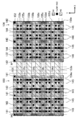
- FIGS. 15 to 17 are plan views illustrating the layout of the transistors P21, P22, N21 and N22 according to this embodiment. Specifically, FIG. 15 shows the VNW FET and layers therebelow, FIG. 16 shows the local interconnect and M1 interconnect above the VNW FET, and FIG. 17 shows the M1 and M2 interconnects. The overall plan view and the cross-sectional view are omitted here because they can be easily inferred from the first embodiment.
- the upper side of the drawing corresponds to the N conductivity type output transistor section 101, and the transistors N21 and N22 in the circuit of FIG. 14 are realized. Further, the lower side of the drawing corresponds to the P conductivity type output transistor section 102, and the transistors P21 and P22 in the circuit of FIG. 14 are realized.
- N-type VNWs V1 are formed in an array of 16 rows in the X direction and 8 rows in the Y direction, for a total of 128 rows.
- a bottom region 211 is formed over substantially the entire surface of the N-conductive output transistor unit 101, and the bottom of the 128 VNWs V 1 is connected to the bottom region 211.
- the VNWs V1 are arranged in pairs in the X direction.
- the group of VNW V1 in every two columns is gn1 to gn8.
- the transistor N21 is realized by the 64 VNWs V1 belonging to the groups gn1, gn4, gn5, gn8.
- the transistor N22 is realized by the 64 VNWs V1 belonging to the groups gn2, gn3, gn6, gn7. There are gaps between the groups gn2 and gn3, between the groups gn4 and gn5, and between the groups gn6 and gn7.
- each of the groups gn1 to gn8 the gates VNW V1 adjacent in the X direction are connected to each other.
- a gate line 221 is drawn from the group gn1 to the left side in the drawing, and a gate line 222 is drawn from the group gn8 to the right side in the drawing.
- the gate wiring 223 is a gate wiring drawn from the group gn2 to the right in the drawing and a gate wiring drawn from the group gn3 to the left in the drawing.
- the four VNWs V1 adjacent in the X direction are connected by the gate wiring 223, and in the groups gn6 and gn7, the four VNWs V1 adjacent in the X direction are the gate wiring 223 It is connected.
- Vias 227a are formed in the gate lines 221, 222 and 223 for connection to the local lines in the upper layer.
- P type VNWs V2 are formed in an array of 16 rows in the X direction and 8 rows in the Y direction, for a total of 128 pieces.
- a bottom region 212 is formed over substantially the entire surface of the P-conductive output transistor portion 102, and the bottom of the 128 VNWs V 2 is connected to the bottom region 212.
- the VNWs V2 are arranged in two rows in the X direction.
- the group of VNW V2 in every two rows is gp1 to gp8.
- the transistor P21 is realized by the 64 VNWs V2 belonging to the groups gp1, gp4, gp5, gp8.
- the transistor P22 is realized by the 64 VNWs V2 belonging to the groups gp2, gp3, gp6, gp7. There are intervals between the groups gp2 and gp3, between the groups gp4 and gp5, and between the groups gp6 and gp7.
- each of the groups gp1 to gp8 the gates VNW V2 adjacent in the X direction are connected to each other.
- a gate line 224 is drawn from the group gp1 to the left side in the drawing, and a gate line 225 is drawn from the group gp8 to the right side in the drawing.
- the gate interconnection 226 is a gate interconnection drawn from the group gp2 to the right in the drawing and a gate interconnection drawn from the group gp3 to the left in the drawing.
- Vias 228a are formed in the gate interconnections 224, 225, and 226 for connection to the upper local interconnections.
- M2 wirings 251, 252, 253, 254, 255, 256a to 256d, 257a to 257d extending in the X direction are formed.
- the M2 wire 251 supplies an output control signal INN1.
- the M2 wire 252 supplies an output control signal INN2.
- the M2 wire 253 supplies the output control signal INP1.
- the M2 wire 254 supplies an output control signal INP2.
- the M2 wiring 255 is a signal line that outputs the output signal OUT, and corresponds to the output signal line in the present disclosure.
- the M2 wires 256 a to 256 d are wires for supplying the power supply voltage VSS and correspond to the power supply wire 7.
- the M2 wires 257 a to 257 d are wires for supplying the power supply voltage VDDIO, and correspond to the power supply wire 6.
- M1 wirings 241, 242, 243, 244, 245, 246, and 247 extending in the Y direction are formed.
- the M1 wiring 241 is disposed in the N conductivity type output transistor unit 101, and is connected to the M2 wiring 251 that supplies the output control signal INN1 via a via.
- the M1 wiring 242 is disposed in the N conductivity type output transistor unit 101, and is connected to the M2 wiring 252 that supplies the output control signal INN2 via a via.
- the M1 wiring 243 is disposed in the P conductivity type output transistor unit 102, and is connected to the M2 wiring 253 that supplies the output control signal INP1 via a via.
- the M1 wiring 244 is disposed in the P conductivity type output transistor unit 102, and is connected to the M2 wiring 254 that supplies the output control signal INP2 via a via.
- the M1 interconnection 245 is disposed in the N-conductivity type output transistor unit 101, and is disposed in pairs on the groups gn1, gn4, gn5, and gn8 of VNW V1 constituting the transistor N21. There is.
- the M1 wiring 245 is connected to the top of the VNW V1 of the groups gn1, gn4, gn5, gn8 via the local wiring 231, and is connected to the M2 wirings 256a to 256d for supplying the power supply voltage VSS via the vias. ing.
- the M1 wire 246 is disposed in the P-conductivity type output transistor unit 102, and is disposed in groups of two each on the groups gp1, gp4, gp5, gp8 of VNW V2 configuring the transistor P21. There is. M1 interconnection 246 is connected to the top of VNW V2 of groups gp1, gp4, gp5 and gp8 via local interconnection 232 and is connected via vias to M2 interconnections 257a-257d supplying power supply voltage VDDIO. ing.
- the M1 wire 247 is disposed across the N conductivity type output transistor portion 101 and the P conductivity type output transistor portion 102.
- M1 interconnections 247 form a pair and are opposed in the Y direction to groups of VNW V1 constituting transistor N22, gn2, gn3, gn6, gn7, and groups of VNW V2 constituting transistor P22 gp2 and gp3. , Gp6 and gp7, respectively.
- the M1 wiring 247 is connected to the top of the VNW V1 of the groups gn2, gn3, gn6, gn7 via the local wiring 231 and connected to the top of the VNW V2 of the groups gp2, gp3, gp6, gp7 via the local wiring 232 And, it is connected to the M2 wiring 255 for outputting the output signal OUT through a via.
- the 64 VNWs V1 belonging to the groups gn1, gn4, gn5, gn8 have the tops of the local wiring 231. It is connected to the M2 wirings 256a to 256d for supplying the power supply voltage VSS via the M1 wiring 245. Also, the bottom is connected to the bottom region 211. In addition, the gate is connected to the M2 wiring 251 which supplies the output control signal INN1 through the gate wirings 221, 222 and 223, the via 227a, and the M1 wiring 241.
- the 64 VNWs V1 belonging to the groups gn2, gn3, gn6, gn7 have the top through the local wiring 231 and the M1 wiring 247. And is connected to the M2 wiring 255 that outputs the output voltage OUT. Also, the bottom is connected via the bottom region 211 to the bottom of the 64 VNWs V1 belonging to the groups gn1, gn4, gn5, gn8.
- the gate is connected to the M2 wiring 252 that supplies the output control signal INN2 through the gate wiring 223, the via 227a, and the M1 wiring 242.
- the transistor N21 in the circuit diagram of FIG. 14 is realized by 64 VNW V1 belonging to the groups gn1, gn4, gn5, gn8 among the 128 VNW V1 formed in the N-conductivity type output transistor portion 101.
- the transistor N22 in the circuit diagram of FIG. 14 is realized by the 64 VNWs V1 belonging to the groups gn2, gn3, gn6, gn7.
- the 64 VNWs V2 belonging to the groups gp1, gp4, gp5 and gp8 have the top through the local interconnect 232 and the M1 interconnect 246. It is connected to the M2 wires 257a to 257d for supplying the power supply voltage VDDIO. Also, the bottom is connected to the bottom region 212. Further, the gate is connected to the M2 wiring 253 for supplying the output control signal INP1 through the gate wirings 224, 225 and 226, the via 228a and the M1 wiring 243.
- the 64 VNWs V2 belonging to the groups gp2, gp3, gp6 and gp7 have the top through the local wire 232 and the M1 wire 247. And is connected to the M2 wiring 255 that outputs the output voltage OUT. Also, the bottom is connected via the bottom region 212 to the bottom of 64 VNWs V2 belonging to the groups gp1, gp4, gp5, gp8.
- the gate is connected to the M2 wiring 254 that supplies the output control signal INP2 through the gate wiring 226, the via 228a, and the M1 wiring 244.
- an output circuit that allows a large current to flow through the output pad can be configured using a VNW FET.
- the transistors N21 and N22 are formed in the N conductivity type output transistor portion 103, and the transistors P21 and P22 are formed in the P conductivity type output transistor portion 104. It shall be.
- the VNWs V1 are arranged in pairs in the X direction.
- the group of VNW V1 in every two columns is gn1 to gn4.
- the transistor N21 is realized by the 64 VNWs V1 belonging to the groups gn1 and gn4.
- the transistor N22 is realized by the 64 VNWs V1 belonging to the groups gn2 and gn3. There is an interval between the groups gn2 and gn3.
- each of the groups gn1 to gn4 the gates VNW V1 adjacent in the X direction are connected to each other.
- a gate line 321 is drawn from the group gn1 to the left side in the drawing, and a gate line 322 is drawn from the group gn4 to the right side in the drawing.
- the gate wiring 323 is a gate wiring drawn from the group gn2 to the right in the drawing and a gate wiring drawn from the group gn3 to the left in the drawing.
- P-type VNWs V2 are formed in an array of 128 rows in eight rows in the X direction and 16 rows in the Y direction.
- a bottom region 312 is formed over substantially the entire surface of the P conductivity type output transistor portion 104, and 128 VNWs V 2 are connected to the bottom region 312 at the bottom.
- a gate line 324 is drawn from the group gp1 to the left side in the drawing, and a gate line 325 is drawn from the group gp4 to the right side in the drawing.
- a gate line 325 is drawn from the group gp4 to the right side in the drawing.
- four VNWs V 2 adjacent in the X direction are connected by the gate wiring 326. That is, gate interconnection 326 is a gate interconnection drawn from group gp2 to the right in the drawing and a gate interconnection drawn from group gp3 to the left in the drawing.
- Vias 328a are formed in the gate wirings 324, 325, and 326 for connection to the upper local wirings.
- M2 wirings 351, 352, 353, 354, 355a to 355e, 356a to 356d, 357a to 357d extending in the X direction are formed.
- the M2 wire 351 supplies an output control signal INN1.
- the M2 wire 352 supplies the output control signal INN2.
- the M2 wire 353 supplies an output control signal INP1.
- the M2 wire 354 supplies an output control signal INP2.
- the M2 wires 355a to 355e are connected to the M3 wire 361 that outputs the output signal OUT via a via.
- the M2 wires 356a to 356d are connected to M3 wires 362a to 362d for supplying the power supply voltage VSS via vias.
- the M2 wires 357a to 357d are connected to M3 wires 363a to 363d for supplying the power supply voltage VDDIO through vias.
- transistor N21 in the circuit diagram of FIG. 14 is realized by 64 VNW V1 belonging to groups gn1 and gn4 out of 128 VNW V1 formed in N-conductivity type output transistor portion 103, and group gn2
- the transistor N22 in the circuit diagram of FIG. 14 is realized by the 64 VNW V1 belonging to.
- transistor P21 in the circuit diagram of FIG. 14 is realized by 64 VNW V2 belonging to groups gp1 and gp4 out of 128 VNW V2 formed in P conductivity type output transistor portion 104, and group gp2 , Gp3 realizes the transistor P22 in the circuit diagram of FIG.
- gate wirings 321 to 326 are formed to extend in the X direction, and have the same wiring width.
- the local interconnections 331 and 332 are formed to extend in the X direction and have the same interconnection width.
- the M1 wires 341 to 348 are formed to extend in the Y direction, and have the same wire width.
- the gate wirings 321 to 326, the local wirings 331 and 332, and the M1 wirings 341 to 348 seem to have the same wiring width, but the wiring widths are made the same in different wiring layers. There is no need, and if the direction and width of the wiring in one wiring layer are the same, manufacture is facilitated and manufacturing accuracy is improved.
- the M3 wire 361 is connected to the top of the VNW V1 of the groups gn2 and gn3 constituting the transistor N22 and the top of the VNW V2 of the groups gp2 and gp3 constituting the transistor P22.
- the resistance value to the output signal line is reduced compared to the case where the M3 wire 361 is connected to the bottom of VNW V1 and V2.
- the bottom region 311 is integrally formed in the N conductivity type output transistor portion 103, and the bottom region 312 is integrally formed in the P conductivity type output transistor portion 104.
- the bottom regions 311 and 312 may be formed separately.
- the bottom region 311 may be divided into groups gn1 and gn2 and groups gn3 and gn4.
Landscapes
- Engineering & Computer Science (AREA)
- Chemical & Material Sciences (AREA)
- Nanotechnology (AREA)
- Physics & Mathematics (AREA)
- Mathematical Physics (AREA)
- Theoretical Computer Science (AREA)
- Crystallography & Structural Chemistry (AREA)
- Design And Manufacture Of Integrated Circuits (AREA)
- Semiconductor Integrated Circuits (AREA)
- General Engineering & Computer Science (AREA)
- Insulated Gate Type Field-Effect Transistor (AREA)
Abstract
VNW FET(縦型ナノワイヤFET)を用いた出力回路のレイアウト構造を提供する。出力回路は、電源(VSS)と出力信号線(53)との間に設けられ、ゲートに出力制御信号(INN)を受ける第1導電型のトランジスタ(N1)を備える。トランジスタ(N1)は、XY方向にアレイ状に配置された複数のVNW FET(V1)を備え、複数のVNW FET(V1)は、トップが出力信号線(53)に接続されており、ボトムに電源電圧(VSS)が与えられており、ゲートに出力制御信号(INN)が与えられる。
Description
本開示は、縦型ナノワイヤ(VNW:Vertical Nanowire)FET(Field Effect Transistor)を備えた半導体集積回路装置に関するものであり、特に、出力回路のレイアウト構造に関する。
半導体集積回路装置は、入出力パッドを介して外部との信号の入出力を行う入出力回路を備える。入出力回路における出力回路については、大電流を流すために、そのレイアウト構造に十分な注意が必要である。
また、LSIの基本構成要素であるトランジスタは、ゲート長の縮小(スケーリング)により、集積度の向上、動作電圧の低減、および動作速度の向上を実現してきた。しかし近年、過度なスケーリングによるオフ電流と、それによる消費電力の著しい増大が問題となっている。この問題を解決するため、トランジスタ構造を従来の平面型から立体型に変更した立体構造トランジスタが盛んに研究されている。その1つとして、縦型ナノワイヤFET(以下、適宜、VNW FETという)が注目されている。
特許文献1では、VNW FETを用いた半導体集積回路のレイアウト構造が開示されている。
特許文献1には、入出力回路における出力回路のように、出力パッドを介して大電流を流す回路に関する具体的なレイアウト構造の開示はない。
本開示は、VNW FETを用いた出力回路のレイアウト構造を提供することを目的とする。
本開示の第1態様では、半導体集積回路から信号を出力するための出力回路は、第1電源と出力信号線との間に設けられ、ゲートに第1出力制御信号を受ける第1導電型の第1トランジスタを備え、前記第1トランジスタは、第1方向と、前記第1方向と垂直をなす第2方向とにアレイ状に配置された、複数の第1VNW FETを備え、前記複数の第1VNW FETは、トップが前記出力信号線に接続されており、ボトムに前記第1電源から第1電源電圧が与えられており、ゲートに前記第1出力制御信号が与えられる。
この態様によると、出力回路において、第1電源と出力信号線との間に設けられ、ゲートに第1出力制御信号を受ける第1導電型の第1トランジスタが、アレイ状に配置された複数の第1VNW FETによって、構成される。これにより、出力パッドを介して大電流を流す出力回路を、VNW FETを用いて構成することができる。
本開示の第2態様では、半導体集積回路から信号を出力するための出力回路は、第1電源と出力信号線との間に直列に設けられた、第1導電型の第1および第2トランジスタを備え、前記第1トランジスタは、ゲートに第1出力制御信号を受け、前記第2トランジスタは、ゲートに第2出力制御信号を受け、前記第1トランジスタは、第1方向と、前記第1方向と垂直をなす第2方向とにアレイ状に配置された、複数の第1VNW FETを備え、前記複数の第1VNW FETは、トップに前記第1電源から第1電源電圧が与えられており、ゲートに前記第1出力制御信号が与えられており、ボトムが第1ボトム領域に接続されており、前記第2トランジスタは、前記第1方向と前記第2方向とにアレイ状に配置された、複数の第2VNW FETを備え、前記複数の第2VNW FETは、トップが前記出力信号線と接続されており、ゲートに前記第2出力制御信号が与えられており、ボトムが前記第1ボトム領域に接続されている。
この態様によると、出力回路において、第1電源と出力信号線との間に直列に設けられ、ゲートに第1および第2出力制御信号をそれぞれ受ける第1導電型の第1および第2トランジスタが、アレイ状に配置された複数の第1VNW FET、および、アレイ状に配置された複数の第2VNW FETによって、それぞれ構成されている。これにより、出力パッドを介して大電流を流す出力回路を、VNW FETを用いて構成することができる。
本開示によると、出力パッドを介して大電流を流す出力回路を、VNW FETを用いて構成することができる。
以下、実施の形態について、図面を参照して説明する。以下の実施の形態では、半導体集積回路装置は複数のIOセルを備えており、このIOセルのうち少なくとも一部は、いわゆる縦型ナノワイヤFET(VNW FET)を備えるものとする。
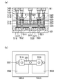
図22はVNW FETの基本構造例を示す模式図であり、(a)は断面図、(b)は平面図である。なお、図22(b)では、メタル配線の図示を省いており、また、理解のしやすさのために、実際の平面視では見えない構成要素を図示している。
図22に示すように、半導体基板501上に、P型ウェル502とN型ウェル503が形成されている。ただし、半導体基板501がP型基板であるとき、P型ウェルを形成しなくてもよい。P型ウェル502上に、N型トランジスタであるVNW FET510が形成されており、N型ウェル503上に、P型トランジスタであるVNW FET520が形成されている。504は絶縁膜、505は層間絶縁膜である。
VNW FET510は、ソース/ドレイン電極となるボトム電極511と、ソース/ドレイン電極となるトップ電極512と、ボトム電極511とトップ電極512との間に、縦方向(基板面に対して垂直方向)に形成されたナノワイヤ513とを備える。ボトム電極511およびトップ電極512は、N導電型にドーピングされている。ナノワイヤ513の少なくとも一部がチャネル領域となる。ナノワイヤ513の周囲にはゲート絶縁膜515が形成されており、さらにその周囲にゲート電極514が形成されている。なお、ゲート電極514はナノワイヤ513の周囲全体を囲んでいてもよいし、ナノワイヤ513の周囲の一部のみを囲んでいてもよい。ゲート電極514がナノワイヤ513の周囲の一部のみを囲んでいる場合は、ゲート絶縁膜515はゲート電極514がナノワイヤ513を囲んでいる部分にのみ形成されていてもよい。
ボトム電極511は、半導体基板501の上面に沿って広がるように形成されたボトム領域516と接続されている。ボトム領域516も、N導電型にドーピングされている。ボトム領域516の表面にはシリサイド領域517が形成されている。また、トップ電極512の周囲に、サイドウォール518が形成されている。トップ電極512の上に、シリサイド領域519が形成されている。ただし、サイドウォール518およびシリサイド領域519は形成しなくてもよい。
同様に、VNW FET520は、ソース/ドレイン電極となるボトム電極521と、ソース/ドレイン電極となるトップ電極522と、ボトム電極521とトップ電極522との間に、縦方向に形成されたナノワイヤ523とを備える。ボトム電極521およびトップ電極522は、P導電型にドーピングされている。ナノワイヤ523の少なくとも一部がチャネル領域となる。ナノワイヤ523の周囲にはゲート絶縁膜525が形成されており、さらにその周囲にゲート電極524が形成されている。
ボトム電極521は、半導体基板501の上面に沿って広がるように形成されたボトム領域526と接続されている。ボトム領域526も、P導電型にドーピングされている。ボトム領域526の表面にはシリサイド領域527が形成されている。また、トップ電極522の周囲に、サイドウォール528が形成されている。トップ電極522の上に、シリサイド領域529が形成されている。ただし、サイドウォール528およびシリサイド領域529は形成しなくてもよい。
図22の構造では、VNW FET510のゲート電極領域514とVNW FET520のゲート電極領域524とが、ゲート配線531によって接続されている。また、ボトム領域516、シリサイド領域519、ゲート配線531、シリサイド領域529およびボトム領域526は、それぞれ、コンタクト532およびコンタクト541を介して、メタル配線層M1に形成された配線542に接続されている。なお、メタル配線層M1のさらに上層に、メタル配線層を積層することができる。
半導体基板501は、例えば、バルクSi、ゲルマニウム、その化合物や合金等によって構成されている。N型ドーパントの例としては、As、P、Sb、N、Cまたはこれらの組み合わせ等がある。P型ドーパントの例としては、B、BF2、In、N、Cまたはこれらの組み合わせ等がある。また、VNW FET510,520の平面形状(ナノワイヤ513,523の横断面形状)は、例えば、円形、矩形、楕円形等であってもよい。
絶縁膜504の材質は、例えば、SiN、SiCN等である。層間絶縁膜505の材料は、例えば、SiO、TEOS、PSG、BPSG、FSG、SiOC、SOG、Spin on Polymers、SiC、または、これらの混合物等がある。シリサイド領域517,527の材質は、例えば、NiSi、CoSi、TiSi、WSi等である。
ゲート電極514,524、および、ゲート配線531の材料は、例えば、TiN、TaN、TiAl、Ti-containing Metal、Ta-containing Metal、Al-containing Metal、W-containing Metal、TiSi、NiSi、PtSi、polysilicon with silicide、これらの組み合わせ等がある。ゲート絶縁膜515,525の材料は、例えば、SiON、Si3N4、Ta2O5、Al2O3、Hf oxide、Ta oxide、Al oxide等がある。また、k値は7以上であることが好ましい。
トップ電極512,522上に設けるシリサイド領域519,529の材料としては、NiSi、CoSi、MoSi、WSi、PtSi、TiSiまたはこれらの組み合わせ等がある。また、他の構成として、W、Cu、Al等のメタルや、TiN、TaN等の合金等、不純物注入された半導体等、またはこれらの組み合わせとしてもよい。サイドウォール518,528の材料としては、例えば、SiN、SiON、SiC、SiCN、SiOCN等がある。
コンタクト532の材料としては、例えば、Ti、TiN、Ta、TaN等がある。また、Cu、Cu-arroy、W、Ag、Au、Ni、Al等がある。あるいは、Co、Ruでもよい。
図23はVNW FETの基本構造例であって、ローカル配線を用いた構造例を示す。図23(a)では、メタル配線層M1と、VNW FET510のトップ電極512およびVNW FET520のトップ電極522との間に、ローカル配線534が形成されている。ボトム領域516,526およびゲート配線531は、それぞれ、コンタクト533、ローカル配線534およびコンタクト541を介して、メタル配線層M1に形成された配線542に接続されている。また、シリサイド領域519,529は、それぞれ、ローカル配線534およびコンタクト541を介して、メタル配線層M1に形成された配線542に接続されている。
図23(b)では、メタル配線層M1とボトム領域516,526との間に、ローカル配線535が形成されている。言い換えると、ローカル配線535は、図23(a)におけるコンタクト533およびローカル配線534が一体となったものに相当する。シリサイド領域536は、ローカル配線535を形成する工程において、エッチングストッパとして用いられる。
以下の説明では、VNW FETのボトム電極、トップ電極、ゲート電極のことを、適宜、単にボトム、トップ、ゲートという。また、縦型ナノワイヤ、トップ、ボトムおよびゲートからなる単位構成が、1個または複数個によって、1個のVNW FETを構成する場合、この単位構成のことを単に「VNW」といい、VNW FETと区別するものとする。
また、本明細書において、「同一配線幅」等のように、幅等が同じであることを意味する表現は、製造上のばらつき範囲を含んでいるものとする。
(第1実施形態)
図1は実施形態に係る半導体集積回路装置(半導体チップ)の全体構成を模式的に示す平面図である。図1では、図面横方向をX方向とし、図面縦方向をY方向としている(以降の図も同様)。図1に示す半導体集積回路装置1は、内部コア回路が形成されたコア領域2と、コア領域2の周囲に設けられ、インターフェース回路(IO回路)が形成されたIO領域3とを備えている。IO領域3には、半導体集積回路装置1の周辺部においてコア領域2を囲むように、IOセル列5が設けられている。図1では図示を簡略化しているが、IOセル列5には、インターフェース回路を構成する複数のIOセル10が並んでいる。
図1は実施形態に係る半導体集積回路装置(半導体チップ)の全体構成を模式的に示す平面図である。図1では、図面横方向をX方向とし、図面縦方向をY方向としている(以降の図も同様)。図1に示す半導体集積回路装置1は、内部コア回路が形成されたコア領域2と、コア領域2の周囲に設けられ、インターフェース回路(IO回路)が形成されたIO領域3とを備えている。IO領域3には、半導体集積回路装置1の周辺部においてコア領域2を囲むように、IOセル列5が設けられている。図1では図示を簡略化しているが、IOセル列5には、インターフェース回路を構成する複数のIOセル10が並んでいる。
ここで、IOセル10は、信号の入力、出力または入出力を行う信号IOセル、接地電位(電源電圧VSS)を供給するための電源IOセル、主にIO領域3に向けて電源(電源電圧VDDIO)を供給するための電源IOセルを含む。例えば、VDDIOは3.3Vである。図1では、コア領域2の図面上側に、信号入出力用のIOセル10Aが配置されており、コア領域2の図面左側に、信号入出力用のIOセル10Bが配置されている。
IO領域3には、IOセル10が並ぶ方向に延びる電源配線6,7が設けられている。電源配線6,7は、半導体集積回路装置1の周辺部にリング状に形成されている(リング電源配線ともいう)。電源配線6は、VDDIOを供給し、電源配線7はVSSを供給する。なお、図1では、電源配線6,7はそれぞれ、単一の配線のように図示されているが、実際には、電源配線6,7はそれぞれ、複数本の配線によって構成される場合もある。また図1では図示を省略しているが、半導体集積回路装置1には、複数の外部接続パッドが配置されている。
図2はIOセル10A,10Bの簡易構成図である。なお、以降の説明では、電源配線6,7はそれぞれ、4本の配線からなるものとしている。図2(a)に示すように、IOセル10Aには、X方向に延びる電源配線6,7が配置されている。そしてIOセル10Aにおいて、電源配線7の下にN導電型出力トランジスタ部101が設けられ、電源配線6の下にP導電型出力トランジスタ部102が設けられている。N導電型出力トランジスタ部101、P導電型出力トランジスタ部102は、IOセル10Aにおいて、チップ外側よりの位置に設けられている。また、図2(b)に示すように、IOセル10Bには、Y方向に延びる電源配線6,7が配置されている。そしてIOセル10Bにおいて、電源配線7の下にN導電型出力トランジスタ部103が設けられ、電源配線6の下にP導電型出力トランジスタ部104が設けられている。N導電型出力トランジスタ部103,P導電型出力トランジスタ部104は、IOセル10Bにおいて、チップ外側よりの位置に設けられている。
図3は本実施形態における出力回路の回路図である。図3の出力回路では、電源VDDIOと出力信号線(出力信号OUTを出力する)との間に、P導電型(以下、適宜、P型という)のトランジスタP1が設けられており、電源VSSと出力信号線との間に、N導電型(以下、適宜、N型という)のトランジスタN1が設けられている。出力制御回路20は出力制御信号INP,INNを出力する。トランジスタP1はゲートに出力制御信号INPを受け、トランジスタN1はゲートに出力制御信号INNを受ける。出力信号OUTは、外部接続パッドに供給される。出力制御信号INP,INNがローレベルのとき、出力信号OUTはハイレベル(VDDIO)になり、出力制御信号INP,INNがハイレベルのとき、出力信号OUTはローレベル(VSS)になる。
以下では、図3の出力回路を構成する2個のトランジスタP1,N1のレイアウト構造について、説明する。ここでは、図2(a)に示すIOセル10Aを例にとり、N導電型出力トランジスタ部101にトランジスタN1が構成されており、P導電型出力トランジスタ部102にトランジスタP1が構成されているものとする。
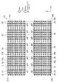
図4~図9は本実施形態に係るトランジスタP1,N1のレイアウト構造の例を示す図であり、図4は全体平面図、図5~図7は層別の平面図、図8および図9は断面図である。具体的には、図5はVNW FETおよびその下の層を示し、図6はVNW FETよりも上のローカル配線およびM1配線を示し、図7はM1およびM2配線を示す。図8は図4の平面視横方向の断面図であり、(a)は線X1-X1’の断面、(b)は線X2-X2’の断面、(c)は線X3-X3’の断面である。図9は図4の平面視縦方向の断面図であり、(a)は線Y1-Y1’の断面、(b)は線Y2-Y2’の断面、(c)は線Y3-Y3’の断面である。
なお、図4等の平面図において縦横に走る点線、および、図8等の断面図において縦に走る点線は、設計時に部品配置を行うために用いるグリッドを示す。グリッドは、X方向において等間隔に配置されており、またY方向において等間隔に配置されている。なお、グリッド間隔は、X方向とY方向とにおいて同じであってもよいし異なっていてもよい。また、グリッド間隔は、層ごとに異なっていてもかまわない。例えば、VNW FETのグリッドとM1配線のグリッドとが、異なる間隔で配置されていてもよい。さらに、各部品は必ずしもグリッド上に配置される必要はない。ただし、製造ばらつきを抑制する観点から、部品はグリッド上に配置される方が好ましい。
また、本実施形態に係るデバイス構造は、図23(a)の構造を前提としている。ただし、図22や図23(b)の構造や、他のデバイス構造を前提とした構造にもなり得る。以降の実施形態についても同様である。また、図を分かりやすくするために、ウェル、STI、各絶縁膜、ボトム上のシリサイド層、トップ上のシリサイド層、および、トップのサイドウォールについては、図示を省略している。以降の図についても同様である。
図4等の平面図において、図面上側がN導電型出力トランジスタ部101に相当し、図3の回路におけるトランジスタN1を実現している。また、図面下側がP導電型出力トランジスタ部102に相当し、図3の回路におけるトランジスタP1を実現している。
図5に示すように、N導電型出力トランジスタ部101では、N型のVNW V1が、X方向に16列、Y方向に8列、計128個、アレイ状に並べて形成されている。この128個のN型のVNW V1によって、トランジスタN1が実現されている。N導電型出力トランジスタ部101には、ほぼ全面にわたってボトム領域11が形成されており、128個のVNW V1は、ボトムがボトム領域11に接続されている。
VNW V1は、X方向において、2列おきに間隔を空けて配置されている。ここでは、2列毎のVNW V1の群のことを、gn1~gn8とする。群gn1~gn8のそれぞれにおいて、X方向に隣り合うVNW V1はゲート同士が接続されている。群gn1から図面左側にゲート配線21が引き出されており、群gn8から図面右側にゲート配線22が引き出されている。群gn2,gn3は、X方向に隣り合う4個のVNW V1がゲート配線23によって接続されている。すなわち、ゲート配線23は、群gn2から図面右側に引き出されたゲート配線であり、かつ、群gn3から図面左側に引き出されたゲート配線である。同様に、群gn4,gn5は、X方向に隣り合う4個のVNW V1がゲート配線23によって接続されており、群gn6,gn7は、X方向に隣り合う4個のVNW V1がゲート配線23によって接続されている。
ゲート配線21,22,23には、その上層のローカル配線と接続するためのビア27aが形成されている。また、ボトム領域11には、その上層のローカル配線と接続するためのビア27bが、群gn1,gn2の間、群gn3,gn4の間、群gn5,gn6の間、および、群gn7,gn8の間に、Y方向に並ぶように、形成されている。
同様に、P導電型出力トランジスタ部102では、P型のVNW V2が、X方向に16列、Y方向に8列、計128個、アレイ状に並べて形成されている。この128個のP型のVNW V2によって、トランジスタP1が実現されている。P導電型出力トランジスタ部102には、ほぼ全面にわたってボトム領域12が形成されており、128個のVNW V2は、ボトムがボトム領域12に接続されている。
VNW V2は、X方向において、2列おきに間隔を空けて配置されている。ここでは、2列毎のVNW V2の群のことを、gp1~gp8とする。群gp1~gp8のそれぞれにおいて、X方向に隣り合うVNW V2はゲート同士が接続されている。群gp1から図面左側にゲート配線24が引き出されており、群gp8から図面右側にゲート配線25が引き出されている。群gp2,gp3は、X方向に隣り合う4個のVNW V2がゲート配線26によって接続されている。すなわち、ゲート配線26は、群gp2から図面右側に引き出されたゲート配線であり、かつ、群gp3から図面左側に引き出されたゲート配線である。同様に、群gp4,gp5は、X方向に隣り合う4個のVNW V2がゲート配線26によって接続されており、群gp6,gp7は、X方向に隣り合う4個のVNW V2がゲート配線26によって接続されている。
ゲート配線24,25,26には、その上層のローカル配線と接続するためのビア28aが形成されている。また、ボトム領域12には、その上層のローカル配線と接続するためのビア28bが、群gp1,gp2の間、群gp3,gp4の間、群gp5,gp6の間、および、群gp7,gp8の間に、Y方向に並ぶように、形成されている。
図6に示すように、各群gn1~gn8において、X方向に隣り合うVNW V1は、トップ同士がローカル配線31によって接続されている。同様に、各群gp1~gp8において、X方向に隣り合うVNW V2は、トップ同士がローカル配線32によって接続されている。
図7に示すように、M2配線層において、X方向に延びるM2配線51,52,53,56a~56d,57a~57dが形成されている。M2配線51は出力制御信号INNを供給する。M2配線52は出力制御信号INPを供給する。M2配線53は出力信号OUTを出力する信号線であり、本開示における出力信号線に相当する。M2配線56a~56dは電源電圧VSSを供給する配線であり、電源配線7に相当する。M2配線57a~57dは電源電圧VDDIOを供給する配線であり、電源配線6に相当する。
M1配線層において、Y方向に延びるM1配線41,42,43,44,45が形成されている。M1配線41は、N導電型出力トランジスタ部101に配置されており、出力制御信号INNを供給するM2配線51とビアを介して接続されている。同様に、M1配線42は、P導電型出力トランジスタ部102に配置されており、出力制御信号INPを供給するM2配線52とビアを介して接続されている。M1配線43は、N導電型出力トランジスタ部101に配置されており、電源電圧VSSを供給するM2配線56a~56dとビアを介して接続されている。M1配線44は、P導電型出力トランジスタ部102に配置されており、電源電圧VDDIOを供給するM2配線57a~57dとビアを介して接続されている。
M1配線45は、N導電型出力トランジスタ部101からP導電型出力トランジスタ部102にわたって配置されている。M1配線45は、2本ずつ組になって配置されており、Y方向において対向する、VNW V1の群gn1~gn8、および,VNW V2の群gp1~gp8の上に、それぞれ、配置されている。M1配線45は、各VNW V1のトップとローカル配線31を介して接続されており、各VNW V2のトップとローカル配線32を介して接続されており、かつ、出力信号OUTを出力するM2配線53とビアを介して接続されている。
以上のようなレイアウト構造により、N導電型出力トランジスタ部101に形成された128個のVNW V1は、トップが、ローカル配線31、M1配線45を介して、出力信号OUTを出力するM2配線53と接続されている。また、ボトムが、ボトム領域11、ビア27b、M1配線43を介して、電源電圧VSSを供給するM2配線56a~56dと接続されている。また、ゲートが、ゲート配線21,22,23、ビア27a、M1配線41を介して、出力制御信号INNを供給するM2配線51と接続されている。したがって、N導電型出力トランジスタ部101に形成された128個のVNW V1によって、図3の回路図におけるトランジスタN1が実現されている。
また、P導電型出力トランジスタ部102に形成された128個のVNW V2は、トップが、ローカル配線32、M1配線45を介して、出力信号OUTを出力するM2配線53と接続されている。また、ボトムが、ボトム領域12、ビア28b、M1配線44を介して、電源電圧VDDIOを供給するM2配線57a~57dと接続されている。また、ゲートが、ゲート配線24,25,26、ビア28a、M1配線42を介して、出力制御信号INPを供給するM2配線52と接続されている。したがって、P導電型出力トランジスタ部102に形成された128個のVNW V2によって、図3の回路図におけるトランジスタP1が実現されている。
したがって、本実施形態により、出力パッドを介して大電流を流す出力回路を、VNW FETを用いて構成することができる。
また、上述した構成では、ゲート配線21~26は、X方向に延びるように形成されており、かつ、同一配線幅である。また、ローカル配線31,32は、X方向に延びるように形成されており、かつ、同一配線幅である。また、M1配線41~45は、Y方向に延びるように形成されており、かつ、同一配線幅である。このように、各配線層において、配線の方向および幅が同一であることによって、製造が容易になり、製造精度が向上する。なお、図示した構成では、ゲート配線21~26、ローカル配線31,32、および、M1配線41~45は、配線幅が互いに同一であるように見えるが、異なる配線層では配線幅を同一にする必要はなく、1つの配線層において配線の方向および幅が同一であれば、製造が容易になり、製造精度が向上する。
また、上述した構成では、平面視で、N導電型出力トランジスタ部101において、VNW V1のトップと接続されたM1配線45は、M1配線43よりも、占める面積が大きい。また、平面視で、P導電型出力トランジスタ部102において、VNW V2のトップと接続されたM1配線45は、M1配線44よりも、占める面積が大きい。これにより、出力信号OUTを出力するM2配線53までの抵抗値を小さくすることができる。また、M2配線53をVNW V1,V2のトップと接続することによって、M2配線53をVNW V1,V2のボトムと接続する場合と比べて、出力信号線までの抵抗値が小さくなる。
また、上述した構成では、各VNW V1について、ゲートへの出力制御信号INNの供給と、ボトムへの電源電圧VSSの供給とが、X方向における両側からなされている。例えば、群gn1のVNW V1では、出力制御信号INNはビア27aを介して図面左側からゲートに与えられ、電源電圧VSSはビア27bを介して図面右側からボトムに与えられる。同様に、各VNW V2では、ゲートへの出力制御信号INPの供給と、ボトムへの電源電圧VDDIOの供給とが、X方向における両側からなされている。例えば、群gp1のVNW V2では、出力制御信号INPはビア28aを介して図面左側からゲートに与えられ、電源電圧VSSはビア28bを介して図面右側からボトムに与えられる。このような構成により、Y方向におけるサイズを小さくすることでき、小面積化を実現することができる。
なお、出力制御信号INNを供給するためのビア27aは、2列以上、並べて配置してもよい。同様に、出力制御信号INPを供給するためのビア28aは、2列以上、並べて配置してもよい。また、ボトム領域11に電源電圧VSSを供給するためのビア27bは、2列以上、並べて配置してもよい。同様に、ボトム領域12に電源電圧VDDIOを供給するためのビア28bは、2列以上、並べて配置してもよい。
また、上の実施形態では、ボトム領域11はN導電型出力トランジスタ部101において一体に形成されており、ボトム領域12はP導電型出力トランジスタ部102において一体に形成されている。この代わりに、ボトム領域11,12は、分割して形成してもかまわない。例えば、ボトム領域11を、群gn1~gn8毎に分割して形成してもよい。ただし、ボトム領域11,12を一体に形成することによって、電源供給の安定化を図ることができる。
(第2実施形態)
第2実施形態では、図3の出力回路を構成する2個のトランジスタP1,N1のレイアウト構造の他の例について、説明する。ここでは、図2(b)に示すIOセル10Bを例にとり、N導電型出力トランジスタ部103がトランジスタN1を構成し、P導電型出力トランジスタ部104がトランジスタP1を構成するものとする。
第2実施形態では、図3の出力回路を構成する2個のトランジスタP1,N1のレイアウト構造の他の例について、説明する。ここでは、図2(b)に示すIOセル10Bを例にとり、N導電型出力トランジスタ部103がトランジスタN1を構成し、P導電型出力トランジスタ部104がトランジスタP1を構成するものとする。
図10~図13は本実施形態に係るトランジスタP1,N1のレイアウト構造の例を示す層別の平面図である。具体的には、図10はVNW FETおよびその下の層を示し、図11はVNW FETよりも上のローカル配線およびM1配線を示し、図12はM1およびM2配線を示し、図13はM2およびM3配線を示す。なお、全体平面図および断面図については、第1実施形態から容易に類推できるため、ここでは省略している。
図10等の平面図において、図面左側がN導電型出力トランジスタ部103に相当し、図3の回路におけるトランジスタN1を実現している。また、図面右側がP導電型出力トランジスタ部104に相当し、図3の回路におけるトランジスタP1を実現している。
図10に示すように、N導電型出力トランジスタ部103では、N型のVNW V1が、X方向に8列、Y方向に16列、計128個、アレイ状に並べて形成されている。この128個のN型のVNW V1によって、トランジスタN1が実現されている。N導電型出力トランジスタ部103には、ほぼ全面にわたってボトム領域111が形成されており、128個のVNW V1は、ボトムがボトム領域111に接続されている。
VNW V1は、X方向において、2列おきに間隔を空けて配置されている。ここでは、2列毎のVNW V1の群のことを、gn1~gn4とする。群gn1~gn4のそれぞれにおいて、X方向に隣り合うVNW V1はゲート同士が接続されている。群gn1から図面左側にゲート配線121が引き出されており、群gn4から図面右側にゲート配線122が引き出されている。群gn2,gn3は、X方向に隣り合う4個のVNW V1がゲート配線123によって接続されている。すなわち、ゲート配線123は、群gn2から図面右側に引き出されたゲート配線であり、かつ、群gn3から図面左側に引き出されたゲート配線である。
ゲート配線121,122,123には、その上層のローカル配線と接続するためのビア127aが形成されている。また、ボトム領域111には、その上層のローカル配線と接続するためのビア127bが、群gn1,gn2の間、および、群gn3,gn4の間に、Y方向に並ぶように、形成されている。
同様に、P導電型出力トランジスタ部104では、P型のVNW V2が、X方向に8列、Y方向に16列、計128個、アレイ状に並べて形成されている。この128個のP型のVNW V2によって、トランジスタP1が実現されている。P導電型出力トランジスタ部104には、ほぼ全面にわたってボトム領域112が形成されており、128個のVNW V2は、ボトムがボトム領域112に接続されている。
VNW V2は、X方向において、2列おきに間隔を空けて配置されている。ここでは、2列毎のVNW V2の群のことを、gp1~gp4とする。群gp1~gp4のそれぞれにおいて、X方向に隣り合うVNW V2はゲート同士が接続されている。群gp1から図面左側にゲート配線124が引き出されており、群gp4から図面右側にゲート配線125が引き出されている。群gp2,gp3は、X方向に隣り合う4個のVNW V2がゲート配線126によって接続されている。すなわち、ゲート配線126は、群gp2から図面右側に引き出されたゲート配線であり、かつ、群gp3から図面左側に引き出されたゲート配線である。
ゲート配線124,125,126には、その上層のローカル配線と接続するためのビア128aが形成されている。また、ボトム領域112には、その上層のローカル配線と接続するためのビア128bが、群gp1,gp2の間、および、群gp3,gp4の間に、Y方向に並ぶように、形成されている。
図11に示すように、各群gn1~gn4において、X方向に隣り合うVNW V1は、トップ同士がローカル配線131によって接続されている。同様に、各群gp1~gp4において、X方向に隣り合うVNW V2は、トップ同士がローカル配線132によって接続されている。
図13に示すように、M3配線層において、Y方向に延びるM3配線161,162a~162d,163a~163dが形成されている。M3配線161は出力信号OUTを出力するものであり、本開示における出力信号線に相当する。M3配線162a~162dは電源電圧VSSを供給する配線であり、電源配線7に相当する。M3配線163a~163dは電源電圧VDDIOを供給する配線であり、電源配線6に相当する。
図12および図13に示すように、M2配線層において、X方向に延びるM2配線151,152,153a~153e,154a~154e,155a~155eが形成されている。M2配線151は出力制御信号INNを供給する。M2配線152は出力制御信号INPを供給する。M2配線153a~153eは、出力信号OUTを出力するM3配線161とビアを介して接続されている。M2配線154a~154eは、電源電圧VSSを供給するM3配線162a~162dとビアを介して接続されている。M2配線155a~155eは、電源電圧VDDIOを供給するM3配線163a~163dとビアを介して接続されている。
図11および図12に示すように、M1配線層において、Y方向に延びるM1配線141,142,143,144,145,146が形成されている。M1配線141は、N導電型出力トランジスタ部103に配置されており、出力制御信号INNを供給するM2配線151とビアを介して接続されている。同様に、M1配線142は、P導電型出力トランジスタ部104に配置されており、出力制御信号INPを供給するM2配線152とビアを介して接続されている。M1配線143は、N導電型出力トランジスタ部103に配置されており、M2配線154a~154eとビアを介して接続されている。M1配線144は、P導電型出力トランジスタ部104に配置されており、M2配線155a~155eとビアを介して接続されている。
M1配線145は、N導電型出力トランジスタ部103に配置されており、2本ずつ組になって、VNW V1の群gn1~gn4の上に、それぞれ、配置されている。M1配線145は、各VNW V1のトップとローカル配線131を介して接続されており、かつ、M2配線153a~153eとビアを介して接続されている。同様に、M1配線146は、P導電型出力トランジスタ部104に配置されており、2本ずつ組になって配置されており、VNW V2の群gp1~gp4の上に、それぞれ、配置されている。M1配線146は、各VNW V1のトップとローカル配線132を介して接続されており、かつ、M2配線153a~153eとビアを介して接続されている。
以上のようなレイアウト構造により、N導電型出力トランジスタ部103に形成された128個のVNW V1は、トップが、ローカル配線131、M1配線145、M2配線153a~153eを介して、出力信号OUTを出力するM3配線161と接続されている。また、ボトムが、ボトム領域111、ビア127b、M1配線143、M2配線154a~154eを介して、電源電圧VSSを供給するM3配線162a~162dと接続されている。また、ゲートが、ゲート配線121,122,123、ビア127a、M1配線141を介して、出力制御信号INNを供給するM2配線151と接続されている。したがって、N導電型出力トランジスタ部103に形成された128個のVNW V1によって、図3の回路図におけるトランジスタN1が実現されている。
また、P導電型出力トランジスタ部104に形成された128個のVNW V2は、トップが、ローカル配線132、M1配線146、M2配線153a~153eを介して、出力信号OUTを出力するM3配線161と接続されている。また、ボトムが、ボトム領域112、ビア128b、M1配線144、M2配線155a~155eを介して、電源電圧VDDIOを供給するM3配線163a~163dと接続されている。また、ゲートが、ゲート配線124,125,126、ビア128a、M1配線142を介して、出力制御信号INPを供給するM2配線152と接続されている。したがって、P導電型出力トランジスタ部104に形成された128個のVNW V2によって、図3の回路図におけるトランジスタP1が実現されている。
したがって、本実施形態により、出力パッドを介して大電流を流す出力回路を、VNW FETを用いて構成することができる。
また、上述した構成では、ゲート配線121~126は、X方向に延びるように形成されており、かつ、同一配線幅である。また、ローカル配線131,132は、X方向に延びるように形成されており、かつ、同一配線幅である。また、M1配線141~146は、Y方向に延びるように形成されており、かつ、同一配線幅である。このように、各配線層において、配線の方向および幅が同一であることによって、製造が容易になり、製造精度が向上する。なお、図示した構成では、ゲート配線121~126、ローカル配線131,132、および、M1配線141~146は、配線幅が互いに同一であるように見えるが、異なる配線層では配線幅を同一にする必要はなく、1つの配線層において配線の方向および幅が同一であれば、製造が容易になり、製造精度が向上する。
また、上述した構成では、平面視で、N導電型出力トランジスタ部103において、VNW V1のトップと接続されたM1配線145は、M1配線143よりも、占める面積が大きい。また、平面視で、P導電型出力トランジスタ部104において、VNW V2のトップと接続されたM1配線146は、M1配線144よりも、占める面積が大きい。これにより、出力信号OUTを出力するM3配線161までの抵抗値を小さくすることができる。また、M3配線161をVNW V1,V2のトップと接続することによって、M3配線161をVNW V1,V2のボトムと接続する場合と比べて、出力信号線までの抵抗値が小さくなる。
また、上述した構成では、各VNW V1について、ゲートへの出力制御信号INNの供給と、ボトムへの電源電圧VSSの供給とが、X方向における両側からなされている。例えば、群gn1のVNW V1では、出力制御信号INNはビア127aを介して図面左側からゲートに与えられ、電源電圧VSSはビア127bを介して図面右側からボトムに与えられる。同様に、各VNW V2では、ゲートへの出力制御信号INPの供給と、ボトムへの電源電圧VDDIOの供給とが、X方向における両側からなされている。例えば、群gp1のVNW V2では、出力制御信号INPはビア128aを介して図面左側からゲートに与えられ、電源電圧VDDIOはビア128bを介して図面右側からボトムに与えられる。このような構成により、Y方向におけるサイズを小さくすることでき、小面積化を実現することができる。
なお、出力制御信号INNを供給するためのビア127aは、2列以上、並べて配置してもよい。同様に、出力制御信号INPを供給するためのビア128aは、2列以上、並べて配置してもよい。また、ボトム領域111に電源電圧VSSを供給するためのビア127bは、2列以上、並べて配置してもよい。同様に、ボトム領域112に電源電圧VDDIOを供給するためのビア128bは、2列以上、並べて配置してもよい。
また、上の実施形態では、ボトム領域111はN導電型出力トランジスタ部103において一体に形成されており、ボトム領域112はP導電型出力トランジスタ部104において一体に形成されている。この代わりに、ボトム領域111,112は、分割して形成してもかまわない。例えば、ボトム領域111を、群gn1~gn4毎に分割して形成してもよい。ただし、ボトム領域111,112を一体に形成することによって、電源供給の安定化を図ることができる。
(第3実施形態)
図14は本実施形態における出力回路の回路図である。図14の出力回路では、電源VDDIOと出力信号線との間に、P型のトランジスタP21,P22が直列に設けられており、電源VSSと出力信号線との間に、N型のトランジスタN21,N22が直列に配置されている。出力制御回路21は出力制御信号INP1,INP2,INN1,INN2を出力する。トランジスタP21はゲートに出力制御信号INP1を受け、トランジスタP22はゲートに出力制御信号INP2を受ける。トランジスタN21はゲートに出力制御信号INN1を受け、トランジスタN22はゲートに出力制御信号INN2を受ける。そして、出力信号OUTは、外部接続パッドに供給される。出力制御信号INP1,INP2,INN1,INN2がローレベルのとき、出力信号OUTはハイレベル(VDDIO)になり、出力制御信号INP1,INP2,INN1,INN2がハイレベルのとき、出力信号OUTはローレベル(VSS)になる。なお、出力制御信号INP1,INP2の一方が固定電位(VSS)であり、出力制御信号INN1,INN2の一方が固定電位(VDDIO)であってもよい。
図14は本実施形態における出力回路の回路図である。図14の出力回路では、電源VDDIOと出力信号線との間に、P型のトランジスタP21,P22が直列に設けられており、電源VSSと出力信号線との間に、N型のトランジスタN21,N22が直列に配置されている。出力制御回路21は出力制御信号INP1,INP2,INN1,INN2を出力する。トランジスタP21はゲートに出力制御信号INP1を受け、トランジスタP22はゲートに出力制御信号INP2を受ける。トランジスタN21はゲートに出力制御信号INN1を受け、トランジスタN22はゲートに出力制御信号INN2を受ける。そして、出力信号OUTは、外部接続パッドに供給される。出力制御信号INP1,INP2,INN1,INN2がローレベルのとき、出力信号OUTはハイレベル(VDDIO)になり、出力制御信号INP1,INP2,INN1,INN2がハイレベルのとき、出力信号OUTはローレベル(VSS)になる。なお、出力制御信号INP1,INP2の一方が固定電位(VSS)であり、出力制御信号INN1,INN2の一方が固定電位(VDDIO)であってもよい。
以下では、図14の出力回路を構成する4個のトランジスタP21,P22,N21,N22のレイアウト構造について、説明する。ここでは、図2(a)に示すIOセル10Aを例にとり、N導電型出力トランジスタ部101にトランジスタN21,N22が構成されており、P導電型出力トランジスタ部102にトランジスタP21,P22が構成されているものとする。
図15~図17は本実施形態に係るトランジスタP21,P22,N21,N22のレイアウト構造の例を示す層別の平面図である。具体的には、図15はVNW FETおよびその下の層を示し、図16はVNW FETよりも上のローカル配線およびM1配線を示し、図17はM1およびM2配線を示す。なお、全体平面図および断面図については、第1実施形態から容易に類推できるため、ここでは省略している。
図15等の平面図において、図面上側がN導電型出力トランジスタ部101に相当し、図14の回路におけるトランジスタN21,N22を実現している。また、図面下側がP導電型出力トランジスタ部102に相当し、図14の回路におけるトランジスタP21,P22を実現している。
図15に示すように、N導電型出力トランジスタ部101では、N型のVNW V1が、X方向に16列、Y方向に8列、計128個、アレイ状に並べて形成されている。N導電型出力トランジスタ部101には、ほぼ全面にわたってボトム領域211が形成されており、128個のVNW V1は、ボトムがボトム領域211に接続されている。
VNW V1は、X方向において、2列一組になって、配置されている。ここでは、2列毎のVNW V1の群のことを、gn1~gn8とする。後述するとおり、群gn1,gn4,gn5,gn8に属する64個のVNW V1によって、トランジスタN21が実現されている。また、群gn2,gn3,gn6,gn7に属する64個のVNW V1によって、トランジスタN22が実現されている。群gn2,gn3の間、群gn4,gn5の間、群gn6,gn7の間には、間隔が空いている。
群gn1~gn8のそれぞれにおいて、X方向に隣り合うVNW V1はゲート同士が接続されている。群gn1から図面左側にゲート配線221が引き出されており、群gn8から図面右側にゲート配線222が引き出されている。群gn2,gn3は、X方向に隣り合う4個のVNW V1がゲート配線223によって接続されている。すなわち、ゲート配線223は、群gn2から図面右側に引き出されたゲート配線であり、かつ、群gn3から図面左側に引き出されたゲート配線である。同様に、群gn4,gn5は、X方向に隣り合う4個のVNW V1がゲート配線223によって接続されており、群gn6,gn7は、X方向に隣り合う4個のVNW V1がゲート配線223によって接続されている。
ゲート配線221,222,223には、その上層のローカル配線と接続するためのビア227aが形成されている。
同様に、P導電型出力トランジスタ部102では、P型のVNW V2が、X方向に16列、Y方向に8列、計128個、アレイ状に並べて形成されている。P導電型出力トランジスタ部102には、ほぼ全面にわたってボトム領域212が形成されており、128個のVNW V2は、ボトムがボトム領域212に接続されている。
VNW V2は、X方向において、2列一組になって、配置されている。ここでは、2列毎のVNW V2の群のことを、gp1~gp8とする。群gp1,gp4,gp5,gp8に属する64個のVNW V2によって、トランジスタP21が実現されている。群gp2,gp3,gp6,gp7に属する64個のVNW V2によって、トランジスタP22が実現されている。群gp2,gp3の間、群gp4,gp5の間、群gp6,gp7の間には、間隔が空いている。
群gp1~gp8のそれぞれにおいて、X方向に隣り合うVNW V2はゲート同士が接続されている。群gp1から図面左側にゲート配線224が引き出されており、群gp8から図面右側にゲート配線225が引き出されている。群gp2,gp3は、X方向に隣り合う4個のVNW V2がゲート配線226によって接続されている。すなわち、ゲート配線226は、群gp2から図面右側に引き出されたゲート配線であり、かつ、群gp3から図面左側に引き出されたゲート配線である。同様に、群gp4,gp5は、X方向に隣り合う4個のVNW V2がゲート配線226によって接続されており、群gp6,gp7は、X方向に隣り合う4個のVNW V2がゲート配線226によって接続されている。
ゲート配線224,225,226には、その上層のローカル配線と接続するためのビア228aが形成されている。
図16に示すように、各群gn1~gn8においてX方向に隣り合うVNW V1は、トップ同士がローカル配線231によって接続されている。同様に、各群gp1~gp8においてX方向に隣り合うVNW V2は、トップ同士がローカル配線232によって接続されている。
図17に示すように、M2配線層において、X方向に延びるM2配線251,252,253,254,255,256a~256d,257a~257dが形成されている。M2配線251は出力制御信号INN1を供給する。M2配線252は出力制御信号INN2を供給する。M2配線253は出力制御信号INP1を供給する。M2配線254は出力制御信号INP2を供給する。M2配線255は出力信号OUTを出力する信号線であり、本開示における出力信号線に相当する。M2配線256a~256dは電源電圧VSSを供給する配線であり、電源配線7に相当する。M2配線257a~257dは電源電圧VDDIOを供給する配線であり、電源配線6に相当する。
図16および図17に示すように、M1配線層において、Y方向に延びるM1配線241,242,243,244,245,246,247が形成されている。M1配線241は、N導電型出力トランジスタ部101に配置されており、出力制御信号INN1を供給するM2配線251とビアを介して接続されている。M1配線242は、N導電型出力トランジスタ部101に配置されており、出力制御信号INN2を供給するM2配線252とビアを介して接続されている。M1配線243は、P導電型出力トランジスタ部102に配置されており、出力制御信号INP1を供給するM2配線253とビアを介して接続されている。M1配線244は、P導電型出力トランジスタ部102に配置されており、出力制御信号INP2を供給するM2配線254とビアを介して接続されている。
M1配線245は、N導電型出力トランジスタ部101に配置されており、2本ずつ組になって、トランジスタN21を構成するVNW V1の群gn1,gn4,gn5,gn8の上に、それぞれ配置されている。M1配線245は、群gn1,gn4,gn5,gn8のVNW V1のトップとローカル配線231を介して接続されており、かつ、電源電圧VSSを供給するM2配線256a~256dとビアを介して接続されている。
M1配線246は、P導電型出力トランジスタ部102に配置されており、2本ずつ組になって、トランジスタP21を構成するVNW V2の群gp1,gp4,gp5,gp8の上に、それぞれ配置されている。M1配線246は、群gp1,gp4,gp5,gp8のVNW V2のトップとローカル配線232を介して接続されており、かつ、電源電圧VDDIOを供給するM2配線257a~257dとビアを介して接続されている。
M1配線247は、N導電型出力トランジスタ部101からP導電型出力トランジスタ部102にわたって配置されている。M1配線247は、2本ずつ組になって、Y方向において対向する、トランジスタN22を構成するVNW V1の群gn2,gn3,gn6,gn7、および,トランジスタP22を構成するVNW V2の群gp2,gp3,gp6,gp7の上に、それぞれ、配置されている。M1配線247は、群gn2,gn3,gn6,gn7のVNW V1のトップとローカル配線231を介して接続され、群gp2,gp3,gp6,gp7のVNW V2のトップとローカル配線232を介して接続され、かつ、出力信号OUTを出力するM2配線255とビアを介して接続されている。
以上のようなレイアウト構造により、N導電型出力トランジスタ部101に形成された128個のVNW V1のうち、群gn1,gn4,gn5,gn8に属する64個のVNW V1は、トップが、ローカル配線231、M1配線245を介して、電源電圧VSSを供給するM2配線256a~256dと接続されている。また、ボトムが、ボトム領域211と接続されている。また、ゲートが、ゲート配線221,222,223、ビア227a、M1配線241を介して、出力制御信号INN1を供給するM2配線251と接続されている。また、N導電型出力トランジスタ部101に形成された128個のVNW V1のうち、群gn2,gn3,gn6,gn7に属する64個のVNW V1は、トップが、ローカル配線231、M1配線247を介して、出力電圧OUTを出力するM2配線255と接続されている。また、ボトムが、ボトム領域211を介して、群gn1,gn4,gn5,gn8に属する64個のVNW V1のボトムと接続されている。また、ゲートが、ゲート配線223、ビア227a、M1配線242を介して、出力制御信号INN2を供給するM2配線252と接続されている。
したがって、N導電型出力トランジスタ部101に形成された128個のVNW V1のうち、群gn1,gn4,gn5,gn8に属する64個のVNW V1によって、図14の回路図におけるトランジスタN21が実現されており、群gn2,gn3,gn6,gn7に属する64個のVNW V1によって、図14の回路図におけるトランジスタN22が実現されている。
また、P導電型出力トランジスタ部102に形成された128個のVNW V2のうち、群gp1,gp4,gp5,gp8に属する64個のVNW V2は、トップが、ローカル配線232、M1配線246を介して、電源電圧VDDIOを供給するM2配線257a~257dと接続されている。また、ボトムが、ボトム領域212と接続されている。また、ゲートが、ゲート配線224,225,226、ビア228a、M1配線243を介して、出力制御信号INP1を供給するM2配線253と接続されている。また、P導電型出力トランジスタ部102に形成された128個のVNW V1のうち、群gp2,gp3,gp6,gp7に属する64個のVNW V2は、トップが、ローカル配線232、M1配線247を介して、出力電圧OUTを出力するM2配線255と接続されている。また、ボトムが、ボトム領域212を介して、群gp1,gp4,gp5,gp8に属する64個のVNW V2のボトムと接続されている。また、ゲートが、ゲート配線226、ビア228a、M1配線244を介して、出力制御信号INP2を供給するM2配線254と接続されている。
したがって、P導電型出力トランジスタ部102に形成された128個のVNW V2のうち、群gp1,gp4,gp5,gp8に属する64個のVNW V2によって、図14の回路図におけるトランジスタP21が実現されており、群gp2,gp3,gp6,gp7に属する64個のVNW V2によって、図14の回路図におけるトランジスタP22が実現されている。
したがって、本実施形態により、出力パッドを介して大電流を流す出力回路を、VNW FETを用いて構成することができる。
なお、上述した構成では、ゲート配線221~226は、X方向に延びるように形成されており、かつ、同一配線幅である。また、ローカル配線231,232は、X方向に延びるように形成されており、かつ、同一配線幅である。また、M1配線241~247は、Y方向に延びるように形成されており、かつ、同一配線幅である。このように、各配線層において、配線の方向および幅が同一であることによって、製造が容易になり、製造精度が向上する。なお、図示した構成では、ゲート配線221~226、ローカル配線231,232、および、M1配線241~247は、配線幅が互いに同一であるように見えるが、異なる配線層では配線幅を同一にする必要はなく、1つの配線層において配線の方向および幅が同一であれば、製造が容易になり、製造精度が向上する。
また、上述した構成では、M2配線255を、トランジスタN22を構成する群gn2,gn3,gn6,gn7のVNW V1のトップ、および,トランジスタP22を構成する群gp2,gp3,gp6,gp7のVNW V2のトップと接続している。これにより、M2配線255をVNW V1,V2のボトムと接続する場合と比べて、出力信号線までの抵抗値が小さくなる。
なお、出力制御信号INN1,INN2を供給するためのビア227aは、2列以上、並べて配置してもよい。同様に、出力制御信号INP1,INP2を供給するためのビア228aは、2列以上、並べて配置してもよい。
また、上の実施形態では、ボトム領域211はN導電型出力トランジスタ部101において一体に形成されており、ボトム領域212はP導電型出力トランジスタ部102において一体に形成されている。この代わりに、ボトム領域211,212は、分割して形成してもかまわない。例えば、ボトム領域211を、群gn1,gn2と、群gn3,gn4と、群gn5,gn6と、群gn7,gn8とで、分割して形成してもよい。
(第4実施形態)
第4実施形態では、図14の出力回路を構成する4個のトランジスタP21,P22,N21,N22のレイアウト構造の他の例について、説明する。ここでは、図2(b)に示すIOセル10Bを例にとり、N導電型出力トランジスタ部103にトランジスタN21,N22が構成されており、P導電型出力トランジスタ部104にトランジスタP21,P22が構成されているものとする。
第4実施形態では、図14の出力回路を構成する4個のトランジスタP21,P22,N21,N22のレイアウト構造の他の例について、説明する。ここでは、図2(b)に示すIOセル10Bを例にとり、N導電型出力トランジスタ部103にトランジスタN21,N22が構成されており、P導電型出力トランジスタ部104にトランジスタP21,P22が構成されているものとする。
図18~図21は本実施形態に係るトランジスタP21,P22,N21,N22のレイアウト構造の例を示す層別の平面図である。具体的には、図18はVNW FETおよびその下の層を示し、図19はVNW FETよりも上のローカル配線およびM1配線を示し、図20はM1およびM2配線を示し、図21はM2およびM3配線を示す。なお、全体平面図および断面図については、第1実施形態から容易に類推できるため、ここでは省略している。
図18等の平面図において、図面左側がN導電型出力トランジスタ部103に相当し、図14の回路におけるトランジスタN21,N22を実現している。また、図面右側がP導電型出力トランジスタ部104に相当し、図14の回路におけるトランジスタP21,P22を実現している。
図18に示すように、N導電型出力トランジスタ部103では、N型のVNW V1が、X方向に8列、Y方向に16列、計128個、アレイ状に並べて形成されている。N導電型出力トランジスタ部103には、ほぼ全面にわたってボトム領域311が形成されており、128個のVNW V1は、ボトムがボトム領域311に接続されている。
VNW V1は、X方向において、2列一組になって、配置されている。ここでは、2列毎のVNW V1の群のことを、gn1~gn4とする。後述するとおり、群gn1,gn4に属する64個のVNW V1によって、トランジスタN21が実現されている。また、群gn2,gn3に属する64個のVNW V1によって、トランジスタN22が実現されている。群gn2,gn3の間には、間隔が空いている。
群gn1~gn4のそれぞれにおいて、X方向に隣り合うVNW V1はゲート同士が接続されている。群gn1から図面左側にゲート配線321が引き出されており、群gn4から図面右側にゲート配線322が引き出されている。群gn2,gn3は、X方向に隣り合う4個のVNW V1がゲート配線323によって接続されている。すなわち、ゲート配線323は、群gn2から図面右側に引き出されたゲート配線であり、かつ、群gn3から図面左側に引き出されたゲート配線である。
ゲート配線321,322,323には、その上層のローカル配線と接続するためのビア327aが形成されている。
同様に、P導電型出力トランジスタ部104では、P型のVNW V2が、X方向に8列、Y方向に16列、計128個、アレイ状に並べて形成されている。P導電型出力トランジスタ部104には、ほぼ全面にわたってボトム領域312が形成されており、128個のVNW V2は、ボトムがボトム領域312に接続されている。
VNW V2は、X方向において、2列一組になって、配置されている。ここでは、2列毎のVNW V1の群のことを、gp1~gp4とする。後述するとおり、群gp1,gp4に属する64個のVNW V2によって、トランジスタP21が実現されている。また、群gp2,gp3に属する64個のVNW V2によって、トランジスタP22が実現されている。群gp2,gp3の間には、間隔が空いている。
群gp1から図面左側にゲート配線324が引き出されており、群gp4から図面右側にゲート配線325が引き出されている。群gp2,gp3は、X方向に隣り合う4個のVNW V2がゲート配線326によって接続されている。すなわち、ゲート配線326は、群gp2から図面右側に引き出されたゲート配線であり、かつ、群gp3から図面左側に引き出されたゲート配線である。
ゲート配線324,325,326には、その上層のローカル配線と接続するためのビア328aが形成されている。
図19に示すように、各群gn1~gn4においてX方向に隣り合うVNW V1は、トップ同士がローカル配線331によって接続されている。同様に、各群gp1~gp4においてX方向に隣り合うVNW V2は、トップ同士がローカル配線332によって接続されている。
図21に示すように、M3配線層において、Y方向に延びるM3配線361,362a~362d,363a~363dが形成されている。M3配線361は出力信号OUTを出力するものであり、本開示における出力信号線に相当する。M3配線362a~362dは電源電圧VSSを供給する配線であり、電源配線7に相当する。M3配線363a~363dは電源電圧VDDIOを供給する配線であり、電源配線6に相当する。
図20および図21に示すように、M2配線層において、X方向に延びるM2配線351,352,353,354,355a~355e,356a~356d,357a~357dが形成されている。M2配線351は出力制御信号INN1を供給する。M2配線352は出力制御信号INN2を供給する。M2配線353は出力制御信号INP1を供給する。M2配線354は出力制御信号INP2を供給する。M2配線355a~355eは、出力信号OUTを出力するM3配線361とビアを介して接続されている。M2配線356a~356dは、電源電圧VSSを供給するM3配線362a~362dとビアを介して接続されている。M2配線357a~357dは、電源電圧VDDIOを供給するM3配線363a~363dとビアを介して接続されている。
図19および図20に示すように、M1配線層において、Y方向に延びるM1配線341,342,343,344,345,346,347,348が形成されている。M1配線341は、N導電型出力トランジスタ部103に配置されており、出力制御信号INN1を供給するM2配線351とビアを介して接続されている。M1配線342は、N導電型出力トランジスタ部103に配置されており、出力制御信号INN2を供給するM2配線352とビアを介して接続されている。同様に、M1配線343は、P導電型出力トランジスタ部104に配置されており、出力制御信号INP1を供給するM2配線353とビアを介して接続されている。M1配線344は、P導電型出力トランジスタ部104に配置されており、出力制御信号INP2を供給するM2配線354とビアを介して接続されている。
M1配線345は、N導電型出力トランジスタ部103において、2本ずつ組になって群gn1,gn4の上にそれぞれ配置されている。M1配線345は、群gn1,gn4のVNW V1のトップとローカル配線331を介して接続されており、かつ、M2配線356a~356dとビアを介して接続されている。M1配線346は、P導電型出力トランジスタ部104において、2本ずつ組になって群gp1,gp4の上に配置されている。M1配線346は、群gp1,gp4のVNW V2のトップとローカル配線332を介して接続されており、かつ、M2配線357a~357dとビアを介して接続されている。
M1配線347は、N導電型出力トランジスタ部103において、2本ずつ組になって群gn2,gn3の上にそれぞれ配置されている。M1配線347は、群gn2,gn3のVNW V1のトップとローカル配線331を介して接続されており、かつ、M2配線355a~355eとビアを介して接続されている。M1配線348は、P導電型出力トランジスタ部104において、2本ずつ組になって群gp2,gp3の上にそれぞれ配置されている。M1配線348は、群gp2,gp3のVNW V2のトップとローカル配線332を介して接続されており、かつ、M2配線355a~355eとビアを介して接続されている。
以上のようなレイアウト構造により、N導電型出力トランジスタ部103に形成された128個のVNW V1のうち、群gn1,gn4に属する64個のVNW V1は、トップが、ローカル配線331、M1配線345、M2配線356a~356dを介して、電源電圧VSSを供給するM3配線362a~366dと接続されている。また、ボトムが、ボトム領域311と接続されている。また、ゲートが、ゲート配線321,322、ビア327a、M1配線341を介して、出力制御信号INN1を供給するM2配線351と接続されている。また、N導電型出力トランジスタ部103に形成された128個のVNW V1のうち、群gn2,gn3に属する64個のVNW V1は、トップが、ローカル配線331、M1配線347、M2配線355a~355eを介して、出力信号OUTを出力するM3配線361と接続されている。また、ボトムが、ボトム領域311を介して、群gn1,gn4に属する64個のVNW V1のボトムと接続されている。また、ゲートが、ゲート配線323、ビア327a、M1配線342を介して、出力制御信号INN2を供給するM2配線352と接続されている。
したがって、N導電型出力トランジスタ部103に形成された128個のVNW V1のうち、群gn1,gn4に属する64個のVNW V1によって、図14の回路図におけるトランジスタN21が実現されており、群gn2,gn3に属する64個のVNW V1によって、図14の回路図におけるトランジスタN22が実現されている。
また、P導電型出力トランジスタ部104に形成された128個のVNW V2のうち、群gp1,gp4に属する64個のVNW V2は、トップが、ローカル配線332、M1配線346、M2配線357a~357dを介して、電源電圧VDDIOを供給するM3配線363a~363dと接続されている。また、ボトムが、ボトム領域312と接続されている。また、ゲートが、ゲート配線324,325、ビア328a、M1配線343を介して、出力制御信号INP1を供給するM2配線353と接続されている。また、P導電型出力トランジスタ部104に形成された128個のVNW V2のうち、群gp2,gp3に属する64個のVNW V2は、トップが、ローカル配線332、M1配線348、M2配線355a~355eを介して、出力信号OUTを出力するM3配線361と接続されている。また、ボトムが、ボトム領域312を介して、群gp1,gp4に属する64個のVNW V2のボトムと接続されている。また、ゲートが、ゲート配線326、ビア328a、M1配線344を介して、出力制御信号INP2を供給するM2配線354と接続されている。
したがって、P導電型出力トランジスタ部104に形成された128個のVNW V2のうち、群gp1,gp4に属する64個のVNW V2によって、図14の回路図におけるトランジスタP21が実現されており、群gp2,gp3に属する64個のVNW V2によって、図14の回路図におけるトランジスタP22が実現されている。
したがって、本実施形態により、出力パッドを介して大電流を流す出力回路を、VNW FETを用いて構成することができる。
なお、上述した構成では、ゲート配線321~326は、X方向に延びるように形成されており、かつ、同一配線幅である。また、ローカル配線331,332は、X方向に延びるように形成されており、かつ、同一配線幅である。また、M1配線341~348は、Y方向に延びるように形成されており、かつ、同一配線幅である。このように、各配線層において、配線の方向および幅が同一であることによって、製造が容易になり、製造精度が向上する。なお、図示した構成では、ゲート配線321~326、ローカル配線331,332、および、M1配線341~348は、配線幅が互いに同一であるように見えるが、異なる配線層では配線幅を同一にする必要はなく、1つの配線層において配線の方向および幅が同一であれば、製造が容易になり、製造精度が向上する。
また、上述した構成では、M3配線361を、トランジスタN22を構成する群gn2,gn3のVNW V1のトップ、および,トランジスタP22を構成する群gp2,gp3のVNW V2のトップと接続している。これにより、M3配線361をVNW V1,V2のボトムと接続する場合と比べて、出力信号線までの抵抗値が小さくなる。
なお、出力制御信号INN1,INN2を供給するためのビア327aは、2列以上、並べて配置してもよい。同様に、出力制御信号INP1,INP2を供給するためのビア328aは、2列以上、並べて配置してもよい。
また、上の実施形態では、ボトム領域311はN導電型出力トランジスタ部103において一体に形成されており、ボトム領域312はP導電型出力トランジスタ部104において一体に形成されている。この代わりに、ボトム領域311,312は、分割して形成してもかまわない。例えば、ボトム領域311を、群gn1,gn2と、群gn3,gn4とで、分割して形成してもよい。
(他の実施形態)
なお、VNW V1,V2の配置位置は、上述した各実施形態で示したものに限られるものではない。また、出力回路の各トランジスタを構成するVNW V1,V2の個数は、上述した各実施形態で示したものに限られるものではない。
なお、VNW V1,V2の配置位置は、上述した各実施形態で示したものに限られるものではない。また、出力回路の各トランジスタを構成するVNW V1,V2の個数は、上述した各実施形態で示したものに限られるものではない。
また、電源電圧VSS,VDDIOを供給する配線は、第1および第3実施形態では、M2配線層にそれぞれ4本ずつ形成されるものとし、第2および第4実施形態では、M3配線層にそれぞれ4本ずつ形成されるものとした。ただし、電源電圧を供給する配線の形態は、これらに限られるものではない。例えば、第1および第3実施形態において、電源電圧を供給する配線は、M2配線層以外の配線層に形成してもよい。あるいは、電源電圧を供給する配線を、複数の配線層に形成してもよいし、4本以外の本数にしてもよい。
また、第1および第2実施形態では、出力制御信号INN,INPを供給する配線は、M2配線層に、それぞれ1本ずつ、形成されるものとし、第3および第4実施形態では、出力制御信号INN1,INN2,INP1,INP2を供給する配線は、M2配線層に、それぞれ1本ずつ、形成されるものとした。ただし、出力制御信号を供給する配線の形態は、これらに限られるものではない。例えば、出力制御信号を供給する配線は、M2配線層以外の配線層に形成してもよいし、複数の配線層に形成してもよいし、同じ配線層に複数本、形成してもよい。また、出力制御信号を供給する配線の配置位置についても、上述した各実施形態で示したものに限られるものではない。例えば、第1実施形態において、出力制御信号INPを供給する配線を、P導電型出力トランジスタ部102の図面下側に配置してもかまわない。
本開示では、出力パッドを介して大電流を流す出力回路を、VNW FETを用いて構成することができるので、例えば半導体チップの性能向上に有用である。
N1 N導電型トランジスタ(第1トランジスタ)
P1 P導電型トランジスタ(第2トランジスタ)
N21 N導電型トランジスタ(第1トランジスタ)
N22 N導電型トランジスタ(第2トランジスタ)
P21 P導電型トランジスタ(第3トランジスタ)
P22 P導電型トランジスタ(第4トランジスタ)
V1 N導電型VNW FET
V2 P導電型VNW FET
INN 第1出力制御信号
INP 第2出力制御信号
INN1 第1出力制御信号
INN2 第2出力制御信号
INP1 第3出力制御信号
INP2 第4出力制御信号
VSS 第1電源、第1電源電圧
VDDIO 第2電源、第2電源電圧
43,44 M1配線(ボトム配線)
45 M1配線(トップ配線)
53 M2配線(出力信号線)
143,144 M1配線(ボトム配線)
145 M1配線(トップ配線)
161 M3配線(出力信号線)
255 M2配線(出力信号線)
361 M3配線(出力信号線)
P1 P導電型トランジスタ(第2トランジスタ)
N21 N導電型トランジスタ(第1トランジスタ)
N22 N導電型トランジスタ(第2トランジスタ)
P21 P導電型トランジスタ(第3トランジスタ)
P22 P導電型トランジスタ(第4トランジスタ)
V1 N導電型VNW FET
V2 P導電型VNW FET
INN 第1出力制御信号
INP 第2出力制御信号
INN1 第1出力制御信号
INN2 第2出力制御信号
INP1 第3出力制御信号
INP2 第4出力制御信号
VSS 第1電源、第1電源電圧
VDDIO 第2電源、第2電源電圧
43,44 M1配線(ボトム配線)
45 M1配線(トップ配線)
53 M2配線(出力信号線)
143,144 M1配線(ボトム配線)
145 M1配線(トップ配線)
161 M3配線(出力信号線)
255 M2配線(出力信号線)
361 M3配線(出力信号線)
Claims (7)
- 半導体集積回路から信号を出力するための出力回路であって、
第1電源と出力信号線との間に設けられ、ゲートに第1出力制御信号を受ける第1導電型の第1トランジスタを備え、
前記第1トランジスタは、
第1方向と、前記第1方向と垂直をなす第2方向とにアレイ状に配置された、複数の第1VNW(Vertical Nanowire:縦型ナノワイヤ) FETを備え、
前記複数の第1VNW FETは、トップが前記出力信号線に接続されており、ボトムに前記第1電源から第1電源電圧が与えられており、ゲートに前記第1出力制御信号が与えられる
ことを特徴とする出力回路。 - 請求項1記載の出力回路において、
第2電源と前記出力信号線との間に設けられ、ゲートに第2出力制御信号を受ける第2導電型の第2トランジスタを備え、
前記第2トランジスタは、
前記第1方向と前記第2方向とにアレイ状に配置された、複数の第2VNW FETを備え、
前記複数の第2VNW FETは、トップが前記出力信号線に接続されており、ボトムに前記第2電源から第2電源電圧が与えられており、ゲートに前記第2出力制御信号が与えられる
ことを特徴とする出力回路。 - 請求項1記載の出力回路において、
前記複数の第1VNW FETの少なくとも一部は、
前記第1方向における一方の側から、ゲートに出力制御信号を受けるとともに、前記第1方向における他方の側から、ボトムに前記第1電源電圧を受ける
ことを特徴とする出力回路。 - 請求項1記載の出力回路において、
第1配線層において、前記複数の第1VNW FETのボトムに接続されたボトム配線、および、前記複数の第1VNW FETのトップに接続されたトップ配線が、前記第2方向に延びるように形成されており、
平面視で、前記複数の第1VNW FETが配置された領域において、前記トップ配線は、前記ボトム配線よりも、占める面積が大きい
ことを特徴とする出力回路。 - 半導体集積回路から信号を出力するための出力回路であって、
第1電源と出力信号線との間に直列に設けられた、第1導電型の第1および第2トランジスタを備え、
前記第1トランジスタは、ゲートに第1出力制御信号を受け、前記第2トランジスタは、ゲートに第2出力制御信号を受け、
前記第1トランジスタは、
第1方向と、前記第1方向と垂直をなす第2方向とにアレイ状に配置された、複数の第1VNW(Vertical Nanowire:縦型ナノワイヤ) FETを備え、
前記複数の第1VNW FETは、トップに前記第1電源から第1電源電圧が与えられており、ゲートに前記第1出力制御信号が与えられており、ボトムが第1ボトム領域に接続されており、
前記第2トランジスタは、
前記第1方向と前記第2方向とにアレイ状に配置された、複数の第2VNW FETを備え、
前記複数の第2VNW FETは、トップが前記出力信号線と接続されており、ゲートに前記第2出力制御信号が与えられており、ボトムが前記第1ボトム領域に接続されている
ことを特徴とする出力回路。 - 請求項5記載の出力回路において、
第2電源と前記出力信号線との間に直列に設けられた、第2導電型の第3および第4トランジスタを備え、
前記第3トランジスタは、ゲートに第3出力制御信号を受け、前記第4トランジスタは、ゲートに第4出力制御信号を受け、
前記第3トランジスタは、
前記第1方向と前記第2方向とにアレイ状に配置された、複数の第3VNW FETを備え、
前記複数の第3VNW FETは、トップに前記第2電源から第2電源電圧が与えられており、ゲートに前記第3出力制御信号が与えられており、ボトムが第2ボトム領域に接続されており、
前記第4トランジスタは、
前記第1方向と前記第2方向とにアレイ状に配置された、複数の第4VNW FETを備え、
前記複数の第4VNW FETは、トップが前記出力信号線と接続されており、ゲートに前記第4出力制御信号が与えられており、ボトムが前記第2ボトム領域に接続されている
ことを特徴とする出力回路。 - 請求項5記載の出力回路において、
前記複数の第1VNW FETと、前記複数の第2VNW FETとは、前記第1方向において隣り合って配置されており、
前記複数の第1VNW FETは、前記第1方向における、前記複数の第2VNW FETと反対の側から、ゲートに前記第1出力制御信号を受け、
前記複数の第2VNW FETは、前記第1方向における、前記複数の第1VNW FETと反対の側から、ゲートに前記第2出力制御信号を受ける
ことを特徴とする出力回路。
Priority Applications (2)
| Application Number | Priority Date | Filing Date | Title |
|---|---|---|---|
| JP2019562882A JPWO2019130965A1 (ja) | 2017-12-25 | 2018-11-28 | 出力回路 |
| US16/905,136 US11295987B2 (en) | 2017-12-25 | 2020-06-18 | Output circuit |
Applications Claiming Priority (2)
| Application Number | Priority Date | Filing Date | Title |
|---|---|---|---|
| JP2017-247638 | 2017-12-25 | ||
| JP2017247638 | 2017-12-25 |
Related Child Applications (1)
| Application Number | Title | Priority Date | Filing Date |
|---|---|---|---|
| US16/905,136 Continuation US11295987B2 (en) | 2017-12-25 | 2020-06-18 | Output circuit |
Publications (1)
| Publication Number | Publication Date |
|---|---|
| WO2019130965A1 true WO2019130965A1 (ja) | 2019-07-04 |
Family
ID=67063439
Family Applications (1)
| Application Number | Title | Priority Date | Filing Date |
|---|---|---|---|
| PCT/JP2018/043800 Ceased WO2019130965A1 (ja) | 2017-12-25 | 2018-11-28 | 出力回路 |
Country Status (3)
| Country | Link |
|---|---|
| US (1) | US11295987B2 (ja) |
| JP (1) | JPWO2019130965A1 (ja) |
| WO (1) | WO2019130965A1 (ja) |
Cited By (2)
| Publication number | Priority date | Publication date | Assignee | Title |
|---|---|---|---|---|
| WO2022224847A1 (ja) * | 2021-04-22 | 2022-10-27 | 株式会社ソシオネクスト | 出力回路 |
| WO2024210011A1 (ja) * | 2023-04-05 | 2024-10-10 | 株式会社ソシオネクスト | 出力回路 |
Families Citing this family (1)
| Publication number | Priority date | Publication date | Assignee | Title |
|---|---|---|---|---|
| WO2019225314A1 (ja) * | 2018-05-22 | 2019-11-28 | 株式会社ソシオネクスト | 半導体集積回路装置 |
Citations (4)
| Publication number | Priority date | Publication date | Assignee | Title |
|---|---|---|---|---|
| JP2008205168A (ja) * | 2007-02-20 | 2008-09-04 | Fujitsu Ltd | 半導体装置及びその製造方法 |
| JP2014503998A (ja) * | 2010-11-26 | 2014-02-13 | サントル ナショナル ドゥ ラ ルシェルシュ シアンティフィク(セー.エヌ.エール.エス) | 網目状の垂直ナノワイヤに実装された電界効果トランジスタデバイスを製造する方法、この方法で製造されるトランジスタデバイス、該トランジスタデバイスを備えた電子デバイス、および、該電子デバイスを少なくとも一つ備えた処理装置 |
| US20160063163A1 (en) * | 2014-08-26 | 2016-03-03 | Synopsys, Inc. | Arrays with compact series connection for vertical nanowires realizations |
| JP2017520908A (ja) * | 2014-06-13 | 2017-07-27 | インテル・コーポレーション | 規則的なグリッドの選択的削減による縦型チャネルトランジスタ製造処理 |
Family Cites Families (2)
| Publication number | Priority date | Publication date | Assignee | Title |
|---|---|---|---|---|
| US9281363B2 (en) | 2014-04-18 | 2016-03-08 | Taiwan Semiconductor Manufacturing Company Ltd. | Circuits using gate-all-around technology |
| WO2019225314A1 (ja) * | 2018-05-22 | 2019-11-28 | 株式会社ソシオネクスト | 半導体集積回路装置 |
-
2018
- 2018-11-28 JP JP2019562882A patent/JPWO2019130965A1/ja active Pending
- 2018-11-28 WO PCT/JP2018/043800 patent/WO2019130965A1/ja not_active Ceased
-
2020
- 2020-06-18 US US16/905,136 patent/US11295987B2/en active Active
Patent Citations (4)
| Publication number | Priority date | Publication date | Assignee | Title |
|---|---|---|---|---|
| JP2008205168A (ja) * | 2007-02-20 | 2008-09-04 | Fujitsu Ltd | 半導体装置及びその製造方法 |
| JP2014503998A (ja) * | 2010-11-26 | 2014-02-13 | サントル ナショナル ドゥ ラ ルシェルシュ シアンティフィク(セー.エヌ.エール.エス) | 網目状の垂直ナノワイヤに実装された電界効果トランジスタデバイスを製造する方法、この方法で製造されるトランジスタデバイス、該トランジスタデバイスを備えた電子デバイス、および、該電子デバイスを少なくとも一つ備えた処理装置 |
| JP2017520908A (ja) * | 2014-06-13 | 2017-07-27 | インテル・コーポレーション | 規則的なグリッドの選択的削減による縦型チャネルトランジスタ製造処理 |
| US20160063163A1 (en) * | 2014-08-26 | 2016-03-03 | Synopsys, Inc. | Arrays with compact series connection for vertical nanowires realizations |
Cited By (2)
| Publication number | Priority date | Publication date | Assignee | Title |
|---|---|---|---|---|
| WO2022224847A1 (ja) * | 2021-04-22 | 2022-10-27 | 株式会社ソシオネクスト | 出力回路 |
| WO2024210011A1 (ja) * | 2023-04-05 | 2024-10-10 | 株式会社ソシオネクスト | 出力回路 |
Also Published As
| Publication number | Publication date |
|---|---|
| US20200321254A1 (en) | 2020-10-08 |
| JPWO2019130965A1 (ja) | 2021-01-14 |
| US11295987B2 (en) | 2022-04-05 |
Similar Documents
| Publication | Publication Date | Title |
|---|---|---|
| US12080804B2 (en) | Semiconductor integrated circuit device | |
| US20220310658A1 (en) | Semiconductor integrated circuit device | |
| CN109564893B (zh) | 半导体芯片 | |
| JPS647508B2 (ja) | ||
| JP2016042568A (ja) | 半導体装置 | |
| US10043571B1 (en) | SRAM structure | |
| US11257826B2 (en) | Semiconductor integrated circuit device | |
| WO2022224847A1 (ja) | 出力回路 | |
| WO2019130965A1 (ja) | 出力回路 | |
| JPWO2019225314A1 (ja) | 半導体集積回路装置 | |
| US11062765B2 (en) | Semiconductor integrated circuit device | |
| US11569218B2 (en) | Semiconductor integrated circuit device | |
| US11296230B2 (en) | Semiconductor integrated circuit device | |
| TWI883367B (zh) | 積體電路系統及積體電路的設計方法 | |
| JP7174263B2 (ja) | 半導体集積回路装置 | |
| WO2019043888A1 (ja) | 半導体集積回路装置 | |
| JP2000223575A (ja) | 半導体装置の設計方法、半導体装置および半導体装置の製造方法 | |
| JP2001035922A (ja) | 半導体集積回路 | |
| JP2019041127A (ja) | 半導体装置 | |
| JP2002134720A (ja) | 半導体装置 | |
| JPS60198748A (ja) | 半導体集積回路装置 | |
| JP2001036050A (ja) | 半導体集積回路用の基本セル | |
| JPH04306863A (ja) | 半導体集積回路装置 |
Legal Events
| Date | Code | Title | Description |
|---|---|---|---|
| 121 | Ep: the epo has been informed by wipo that ep was designated in this application |
Ref document number: 18895687 Country of ref document: EP Kind code of ref document: A1 |
|
| ENP | Entry into the national phase |
Ref document number: 2019562882 Country of ref document: JP Kind code of ref document: A |
|
| NENP | Non-entry into the national phase |
Ref country code: DE |
|
| 122 | Ep: pct application non-entry in european phase |
Ref document number: 18895687 Country of ref document: EP Kind code of ref document: A1 |