WO2019124155A1 - 液晶表示素子 - Google Patents
液晶表示素子 Download PDFInfo
- Publication number
- WO2019124155A1 WO2019124155A1 PCT/JP2018/045435 JP2018045435W WO2019124155A1 WO 2019124155 A1 WO2019124155 A1 WO 2019124155A1 JP 2018045435 W JP2018045435 W JP 2018045435W WO 2019124155 A1 WO2019124155 A1 WO 2019124155A1
- Authority
- WO
- WIPO (PCT)
- Prior art keywords
- liquid crystal
- group
- substrate
- layer
- alignment
- Prior art date
- Legal status (The legal status is an assumption and is not a legal conclusion. Google has not performed a legal analysis and makes no representation as to the accuracy of the status listed.)
- Ceased
Links
- 0 *=*C1CCC(*I2=CIC2)CC1 Chemical compound *=*C1CCC(*I2=CIC2)CC1 0.000 description 2
- MYMIRSJEWWFFBM-UHFFFAOYSA-N CCCCCCc(cc1)ccc1-c(cc1)cc(CC)c1-c(cc1)ccc1OCCO Chemical compound CCCCCCc(cc1)ccc1-c(cc1)cc(CC)c1-c(cc1)ccc1OCCO MYMIRSJEWWFFBM-UHFFFAOYSA-N 0.000 description 2
- JFRKUOICIREZAT-UHFFFAOYSA-N CCCCCCc(cc1)ccc1-c(cc1)cc(CC)c1-c(cc1)cc(CCOC(C(C)=C)=O)c1OCCO Chemical compound CCCCCCc(cc1)ccc1-c(cc1)cc(CC)c1-c(cc1)cc(CCOC(C(C)=C)=O)c1OCCO JFRKUOICIREZAT-UHFFFAOYSA-N 0.000 description 1
- LGHOMLSUJPIBKW-HHHXNRCGSA-N CCCCCCc(cc1)ccc1-c(cc1)cc(CC)c1-c(cc1)cc(C[I]([O](CCC[I]([C@H](C)I)C2=C)C2=O)I)c1OC[I](O)I Chemical compound CCCCCCc(cc1)ccc1-c(cc1)cc(CC)c1-c(cc1)cc(C[I]([O](CCC[I]([C@H](C)I)C2=C)C2=O)I)c1OC[I](O)I LGHOMLSUJPIBKW-HHHXNRCGSA-N 0.000 description 1
Images




Classifications
-
- G—PHYSICS
- G02—OPTICS
- G02F—OPTICAL DEVICES OR ARRANGEMENTS FOR THE CONTROL OF LIGHT BY MODIFICATION OF THE OPTICAL PROPERTIES OF THE MEDIA OF THE ELEMENTS INVOLVED THEREIN; NON-LINEAR OPTICS; FREQUENCY-CHANGING OF LIGHT; OPTICAL LOGIC ELEMENTS; OPTICAL ANALOGUE/DIGITAL CONVERTERS
- G02F1/00—Devices or arrangements for the control of the intensity, colour, phase, polarisation or direction of light arriving from an independent light source, e.g. switching, gating or modulating; Non-linear optics
- G02F1/01—Devices or arrangements for the control of the intensity, colour, phase, polarisation or direction of light arriving from an independent light source, e.g. switching, gating or modulating; Non-linear optics for the control of the intensity, phase, polarisation or colour
- G02F1/13—Devices or arrangements for the control of the intensity, colour, phase, polarisation or direction of light arriving from an independent light source, e.g. switching, gating or modulating; Non-linear optics for the control of the intensity, phase, polarisation or colour based on liquid crystals, e.g. single liquid crystal display cells
- G02F1/137—Devices or arrangements for the control of the intensity, colour, phase, polarisation or direction of light arriving from an independent light source, e.g. switching, gating or modulating; Non-linear optics for the control of the intensity, phase, polarisation or colour based on liquid crystals, e.g. single liquid crystal display cells characterised by the electro-optical or magneto-optical effect, e.g. field-induced phase transition, orientation effect, guest-host interaction or dynamic scattering
-
- C—CHEMISTRY; METALLURGY
- C09—DYES; PAINTS; POLISHES; NATURAL RESINS; ADHESIVES; COMPOSITIONS NOT OTHERWISE PROVIDED FOR; APPLICATIONS OF MATERIALS NOT OTHERWISE PROVIDED FOR
- C09K—MATERIALS FOR MISCELLANEOUS APPLICATIONS, NOT PROVIDED FOR ELSEWHERE
- C09K19/00—Liquid crystal materials
- C09K19/04—Liquid crystal materials characterised by the chemical structure of the liquid crystal components, e.g. by a specific unit
- C09K19/38—Polymers
-
- C—CHEMISTRY; METALLURGY
- C09—DYES; PAINTS; POLISHES; NATURAL RESINS; ADHESIVES; COMPOSITIONS NOT OTHERWISE PROVIDED FOR; APPLICATIONS OF MATERIALS NOT OTHERWISE PROVIDED FOR
- C09K—MATERIALS FOR MISCELLANEOUS APPLICATIONS, NOT PROVIDED FOR ELSEWHERE
- C09K19/00—Liquid crystal materials
- C09K19/52—Liquid crystal materials characterised by components which are not liquid crystals, e.g. additives with special physical aspect: solvents, solid particles
- C09K19/54—Additives having no specific mesophase characterised by their chemical composition
- C09K19/56—Aligning agents
-
- G—PHYSICS
- G02—OPTICS
- G02F—OPTICAL DEVICES OR ARRANGEMENTS FOR THE CONTROL OF LIGHT BY MODIFICATION OF THE OPTICAL PROPERTIES OF THE MEDIA OF THE ELEMENTS INVOLVED THEREIN; NON-LINEAR OPTICS; FREQUENCY-CHANGING OF LIGHT; OPTICAL LOGIC ELEMENTS; OPTICAL ANALOGUE/DIGITAL CONVERTERS
- G02F1/00—Devices or arrangements for the control of the intensity, colour, phase, polarisation or direction of light arriving from an independent light source, e.g. switching, gating or modulating; Non-linear optics
- G02F1/01—Devices or arrangements for the control of the intensity, colour, phase, polarisation or direction of light arriving from an independent light source, e.g. switching, gating or modulating; Non-linear optics for the control of the intensity, phase, polarisation or colour
- G02F1/13—Devices or arrangements for the control of the intensity, colour, phase, polarisation or direction of light arriving from an independent light source, e.g. switching, gating or modulating; Non-linear optics for the control of the intensity, phase, polarisation or colour based on liquid crystals, e.g. single liquid crystal display cells
-
- G—PHYSICS
- G02—OPTICS
- G02F—OPTICAL DEVICES OR ARRANGEMENTS FOR THE CONTROL OF LIGHT BY MODIFICATION OF THE OPTICAL PROPERTIES OF THE MEDIA OF THE ELEMENTS INVOLVED THEREIN; NON-LINEAR OPTICS; FREQUENCY-CHANGING OF LIGHT; OPTICAL LOGIC ELEMENTS; OPTICAL ANALOGUE/DIGITAL CONVERTERS
- G02F1/00—Devices or arrangements for the control of the intensity, colour, phase, polarisation or direction of light arriving from an independent light source, e.g. switching, gating or modulating; Non-linear optics
- G02F1/01—Devices or arrangements for the control of the intensity, colour, phase, polarisation or direction of light arriving from an independent light source, e.g. switching, gating or modulating; Non-linear optics for the control of the intensity, phase, polarisation or colour
- G02F1/13—Devices or arrangements for the control of the intensity, colour, phase, polarisation or direction of light arriving from an independent light source, e.g. switching, gating or modulating; Non-linear optics for the control of the intensity, phase, polarisation or colour based on liquid crystals, e.g. single liquid crystal display cells
- G02F1/133—Constructional arrangements; Operation of liquid crystal cells; Circuit arrangements
- G02F1/1333—Constructional arrangements; Manufacturing methods
- G02F1/1337—Surface-induced orientation of the liquid crystal molecules, e.g. by alignment layers
-
- G—PHYSICS
- G02—OPTICS
- G02F—OPTICAL DEVICES OR ARRANGEMENTS FOR THE CONTROL OF LIGHT BY MODIFICATION OF THE OPTICAL PROPERTIES OF THE MEDIA OF THE ELEMENTS INVOLVED THEREIN; NON-LINEAR OPTICS; FREQUENCY-CHANGING OF LIGHT; OPTICAL LOGIC ELEMENTS; OPTICAL ANALOGUE/DIGITAL CONVERTERS
- G02F1/00—Devices or arrangements for the control of the intensity, colour, phase, polarisation or direction of light arriving from an independent light source, e.g. switching, gating or modulating; Non-linear optics
- G02F1/01—Devices or arrangements for the control of the intensity, colour, phase, polarisation or direction of light arriving from an independent light source, e.g. switching, gating or modulating; Non-linear optics for the control of the intensity, phase, polarisation or colour
- G02F1/13—Devices or arrangements for the control of the intensity, colour, phase, polarisation or direction of light arriving from an independent light source, e.g. switching, gating or modulating; Non-linear optics for the control of the intensity, phase, polarisation or colour based on liquid crystals, e.g. single liquid crystal display cells
- G02F1/133—Constructional arrangements; Operation of liquid crystal cells; Circuit arrangements
- G02F1/1333—Constructional arrangements; Manufacturing methods
- G02F1/1335—Structural association of cells with optical devices, e.g. polarisers or reflectors
-
- G—PHYSICS
- G02—OPTICS
- G02F—OPTICAL DEVICES OR ARRANGEMENTS FOR THE CONTROL OF LIGHT BY MODIFICATION OF THE OPTICAL PROPERTIES OF THE MEDIA OF THE ELEMENTS INVOLVED THEREIN; NON-LINEAR OPTICS; FREQUENCY-CHANGING OF LIGHT; OPTICAL LOGIC ELEMENTS; OPTICAL ANALOGUE/DIGITAL CONVERTERS
- G02F1/00—Devices or arrangements for the control of the intensity, colour, phase, polarisation or direction of light arriving from an independent light source, e.g. switching, gating or modulating; Non-linear optics
- G02F1/01—Devices or arrangements for the control of the intensity, colour, phase, polarisation or direction of light arriving from an independent light source, e.g. switching, gating or modulating; Non-linear optics for the control of the intensity, phase, polarisation or colour
- G02F1/13—Devices or arrangements for the control of the intensity, colour, phase, polarisation or direction of light arriving from an independent light source, e.g. switching, gating or modulating; Non-linear optics for the control of the intensity, phase, polarisation or colour based on liquid crystals, e.g. single liquid crystal display cells
- G02F1/133—Constructional arrangements; Operation of liquid crystal cells; Circuit arrangements
- G02F1/136—Liquid crystal cells structurally associated with a semi-conducting layer or substrate, e.g. cells forming part of an integrated circuit
- G02F1/1362—Active matrix addressed cells
- G02F1/1368—Active matrix addressed cells in which the switching element is a three-electrode device
Definitions
- the present invention relates to a liquid crystal display device.
- liquid crystal display devices such as liquid crystal panels and liquid crystal displays
- the state of alignment of liquid crystal molecules is changed by an external stimulus such as an electric field, and the change in optical characteristics accompanying this is used for display.
- a liquid crystal display element has a configuration in which liquid crystal molecules are filled in a gap between two transparent substrates, and the liquid crystal molecules are arranged in advance in a specific direction on the surface of the substrate in contact with the liquid crystal molecules. It is general to form an alignment film for making it.
- Patent Document 1 instead of lauryl acrylate, which has relatively weak interaction with liquid crystal molecules, a highly linear monofunctional biphenyl monomer having an octyl group and a low straight line having a stearyl group are shown.
- a liquid crystal composition containing a spontaneous alignment material that suppresses a decrease in voltage holding ratio by a liquid crystal composition containing a functional biphenyl monomer is described.
- Patent Document 2 discloses various liquid crystal compositions containing a polymerizable self-orienting additive for controlling the alignment of liquid crystal molecules instead of an alignment film, and a nematic LC medium and a polymerizable self-orienting additive,
- a liquid crystal composition optionally comprising a polymerisable compound
- a test cell without an alignment layer
- it has spontaneous homeotropic (vertical) alignment with respect to the substrate surface and this vertical alignment is stable until the clearing point It is stated that the formed VA cell can be reversibly switched by voltage application.
- a composition including two hydrophobic monomers each having a long alkyl chain and a biphenyl skeleton as shown in the above-mentioned Patent Document 1 has an interaction with liquid crystal molecules of a liquid crystal layer filled between a pair of substrates. Though it is considered to be stronger than lauryl acrylate, the problem is that the polymerizable self-orientation additive itself is not immobilized on the substrate and that the orientation direction of the liquid crystal molecules can not be regulated due to the low adsorption power to the substrate. .
- Patent Documents 1 and 2 describe polymerizable self-orientation additives that interact directly with the substrate, but do not consider the interaction with the irregularities on the substrate surface or the overcoat layer on the substrate surface. Therefore, there arises a problem that alignment unevenness occurs on the overcoat layer.
- the problem to be solved by the present invention is to provide a liquid crystal display device excellent in vertical alignment with an insulating layer, particularly with respect to an organic insulating layer.
- the liquid crystal display element according to the present invention exhibits high compatibility and excellent vertical alignment to liquid crystal molecules.
- the liquid crystal display element according to the present invention exhibits excellent spreadability (wet spread) with respect to a substrate.
- the liquid crystal display element according to the present invention can reduce or eliminate the alignment unevenness.
- FIG. 1 is a view schematically showing the configuration of a vertical electric field type liquid crystal display device.
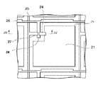
- FIG. 2 is an enlarged plan view of a region surrounded by a line II of the electrode layer 3 including the thin film transistor formed on the substrate in FIG.
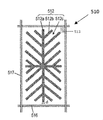
- FIG. 3 shows a modification of the electrode layer 3 including the thin film transistor of FIG.
- FIG. 4 is a cross-sectional view of the liquid crystal display element shown in FIG. 1 cut along the line III-III in FIG.
- FIG. 5 is a cross-sectional view of the thin film transistor in which the region surrounded by the line IV in FIG. 4 is enlarged.
- FIG. 6 is a cross-sectional view showing a modification of FIG.
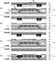
- FIG. 7 shows a cross-sectional view of a preferred vertical electric field liquid crystal display element of the present invention.
- FIG. 8 is a view showing experimental data of the present example.
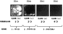
- FIG. 9 is an image showing the experimental result of this example.
- a first aspect of the present invention relates to a first substrate and a second substrate provided opposite to the first substrate, and a first insulating layer and a first electrode provided on the first substrate. And a liquid crystal layer provided between the first substrate and the second substrate and containing an alignment imparting component for imparting alignment to liquid crystal molecules, the liquid crystal layer comprising the first liquid crystal layer It is a liquid crystal display element characterized by being formed from a liquid crystal composition containing an alignment imparting compound having two or more adsorption sites capable of interacting with an insulating layer.
- the alignment imparting component contained in the liquid crystal layer can control the alignment of liquid crystal molecules constituting the liquid crystal layer, and thus, an alignment film (rubbing alignment film) conventionally used to align liquid crystal molecules in a certain direction
- an alignment film rubbing alignment film
- the effect of regulating the alignment direction of liquid crystal molecules in the state of no voltage application can be improved by using the photo alignment film or the like instead of or in combination with the alignment film.
- the liquid crystal layer containing the above-mentioned alignment imparting component includes, for example, an alignment imparting compound having two or more adsorption sites that interact with an insulating layer such as SiNx or overcoat layer, and aligning liquid crystal molecules in a certain direction. Since the alignment imparting component interacts with the insulating layer at multiple points because it is formed of a liquid crystal composition, the fixing force with respect to the substrate is improved, and the alignment regulating force with respect to liquid crystal molecules is greater. Become.
- FIGS. 1 to 6 illustrate a vertical electric field liquid crystal display device as a preferred example of the liquid crystal display device according to the present invention, but the present invention is not limited thereto.
- FIG. 1 is a view schematically showing the configuration of a vertical electric field type liquid crystal display device. Moreover, in FIG. 1, for convenience of explanation, the respective components are illustrated separately for the sake of explanation.
- FIGS. 2 and 3 are enlarged plan views of the region surrounded by the II line of the electrode layer 3 (also referred to as the thin film transistor layer 3) including the thin film transistor formed on the substrate in FIG.
- FIG. 3 shows a modification of the electrode layer 3 including the thin film transistor of FIG.
- FIG. 4 is a cross-sectional view of the liquid crystal display element shown in FIG. 1 cut along the line III-III in FIG.
- FIG. 5 is a diagram showing an aspect of the thin film transistor in the region IV of FIG.
- FIG. 6 is a view showing a modification of the cross-sectional view of the liquid crystal display element shown in FIG. 4, and is a view showing the structure of a so-called color filter on array.
- the configuration of the liquid crystal display element 10 is an electrode provided with a first polarizing layer 1 on one surface, and a thin film transistor for controlling the pixel electrode and the pixel electrode provided in each pixel on the other surface.
- a first substrate 2 comprising a layer 3 and a second polarizing layer 8 on one side and a (transparent) electrode layer 3 '(also called common electrode layer 3') and a color on the other side
- a liquid crystal layer 5 (a liquid crystal composition containing a second substrate 7 provided with a filter 6 and an alignment imparting compound for giving alignment to liquid crystal molecules) sandwiched between the first substrate 2 and the second substrate 7 (Formed of). Further, in the liquid crystal display element shown in FIG.
- the liquid crystal molecules in the liquid crystal layer 5 are aligned with the major axis direction of the liquid crystal molecules when the voltage is not applied substantially perpendicular to the substrates 2 and 7.
- the major axis direction of the liquid crystal molecules is aligned substantially parallel to the substrates 2 and 7, and the major axis direction of the liquid crystal molecules is reversibly controlled in response to a voltage.
- the alignment imparting compound and the alignment imparting component according to the present invention impart liquid crystal molecules in the liquid crystal layer with an alignment substantially perpendicular to the first substrate 2 and / or the second substrate 7. Play a role.
- the alignment imparting compound or the alignment imparting component in the liquid crystal layer can be stably present in the vicinity of the interface of the liquid crystal layer since it has an adsorption site, and the alignment imparting compound or the alignment imparting component when no voltage is applied.
- liquid crystal molecules are aligned substantially perpendicularly to the first substrate 2 and / or the second substrate 7.
- An alignment layer (not shown) is formed on the surface of the electrode (layer) 3 or the common electrode layer 3 'so as to be adjacent to the liquid crystal layer 5 according to the present invention and in direct contact with the liquid crystal composition constituting the liquid crystal layer 5. It may be formed on at least one side if necessary. That is, the alignment layer 4 may be provided between the liquid crystal layer 5 and the electrode layer 3 ′, or the alignment layer 4 may be provided between the liquid crystal layer 5 and the electrode layer 3.
- the alignment film and the alignment imparting component of the present invention in combination, the effect of restricting the alignment direction of liquid crystal molecules in a state of no voltage application can be improved.
- one of the preferable embodiments of the liquid crystal display element 10 according to the present invention is a first polarizing layer 1, a first substrate 2, an electrode layer 3 including a thin film transistor, a liquid crystal layer 5 including an alignment imparting component, a transparent electrode Layer) 3 ', the color filter 6, the second substrate 7 and the second polarizing layer 8 are sequentially laminated.
- the color filter 6 may be provided on the electrode layer 3 including the thin film transistor on the first substrate.
- the arrow in FIG. 1 shows the direction of the light from the backlight attached to a liquid crystal display element.
- the tip of the arrow corresponds to the so-called visual side.
- FIG. 2 is a view showing an “′ ′ ′ -type (inverted L-shaped) as an example of the shape of the electrode of one pixel of the electrode layer 3, that is, the so-called pixel electrode 21, and the electrode formed on the substrate 2 in FIG. It is the top view to which the area
- the pixel electrode 21 is disposed for each display pixel, and a slit-like opening is formed.
- the common electrode and the pixel electrode are, for example, transparent electrodes formed of ITO (Indium Tin Oxide), and the electrode layer 3 is a gate extending along a row in which a plurality of display pixels are arranged in the display portion of the liquid crystal display element.
- a bus line 26 (GBL1, GBL2... GBLm), a source bus line 25 (SBL1, SBL2... SBLm) extending along a column in which a plurality of display pixels are arranged, a gate bus line 26 and a source bus line 25
- a thin film transistor region IV in FIG.
- the gate electrode 28 of the thin film transistor is electrically connected to the corresponding gate bus line 26, and the source electrode 27 of the thin film transistor is electrically connected to the corresponding source bus line 25. Furthermore, the drain electrode 24 of the thin film transistor is electrically connected to the corresponding pixel electrode.
- the electrode structure including the thin film transistor of the liquid crystal display element according to the present invention in the electrode layer 3 including the thin film transistor formed on the surface of the first substrate 2 In a region where gate bus lines 26 for supplying and source bus lines 25 for supplying display signals cross each other, and are surrounded by the plurality of gate bus lines 26 and the plurality of source bus lines 25.
- the pixel electrodes 21 are formed in a matrix.
- a thin film transistor including a source electrode 27, a drain electrode 24, and a gate electrode 28 in the vicinity of an intersection where the gate bus line 26 and the source bus line 25 intersect with each other as a switch element for supplying a display signal to the pixel electrode 21 Are provided adjacent to the pixel electrode 21.
- a storage capacitor may be provided in a region surrounded by the plurality of gate bus lines and the plurality of source bus lines to store the potential written for each pixel.
- the insulating layer 30 is exposed in the thin film transistor portion (region IV in FIG. 4) to which the drain electrode 24 is connected and the edge region of the pixel not covering the pixel electrode 21 (electrode layer 3). It is done.
- a compound (alignment imparting compound) for aligning liquid crystal molecules in a certain direction is added to the liquid crystal layer instead of an alignment film such as a so-called spontaneous alignment agent.
- the insulating layer 30 and the thin film transistor having unevenness are in direct contact with the liquid crystal layer 5.
- an orientation imparting component is formed in a state where it is immobilized at multiple points with the insulating layer 30 using an orientation imparting compound provided with an adsorption site that can be immobilized at multiple points with the insulating layer 30 in one molecule.
- the orientation imparting component 4 can uniformly cover the thin film transistor having a concavo-convex portion, the insulating layer 30, and the like, and as shown in the embodiment, the insulating layer 30 and the liquid crystal It is considered that alignment unevenness can be suppressed in the region in contact with the layer 5 and in the region of the thin film transistor having unevenness. Further, the alignment imparting compound having an adsorption site that can be immobilized at multiple points or the alignment imparting component imparts liquid crystal molecules with an alignment in a direction substantially perpendicular to the first substrate 2 or the second substrate 7. Is preferred.
- the electrode layer 3 includes a gate driver and a source driver as drive means for driving a plurality of display pixels, and the gate driver and the source driver are disposed around the liquid crystal display unit.
- the plurality of gate bus lines are electrically connected to the output terminal of the gate driver, and the plurality of source bus lines are electrically connected to the output terminal of the source driver.
- the gate driver sequentially applies the on voltage to the plurality of gate bus lines, and supplies the on voltage to the gate electrode of the thin film transistor electrically connected to the selected gate bus line. Electrical conduction is established between the source and drain electrodes of the thin film transistor in which the on voltage is supplied to the gate electrode.
- the source driver supplies an output signal corresponding to each of the plurality of source bus lines. The signal supplied to the source bus line is applied to the corresponding pixel electrode through the thin film transistor which is conducted between the source and drain electrodes.
- the operation of the gate driver and the source driver is controlled by a display processing unit (also referred to as a control circuit) disposed outside the liquid crystal display element.
- the region surrounded by the gate bus line 26 and the source bus line 25 is formed in a substantially "" "shape
- the shape of the pixel electrode is not limited to this. It may be a pixel electrode of a fishbone structure shown by.
- FIG. 3 is a view showing a “fish bone” type as another example of the shape of the pixel electrode of one pixel of the electrode layer 3 and is surrounded by the II line of the electrode layer 3 formed on the substrate 2 in FIG. It is the top view to which the isolated area was expanded.
- a so-called fishbone type electrode as shown in FIG. 3 is preferable from the viewpoint of the stability of the orientation.
- this electrode is comprised from transparent electrodes, such as ITO, and the slit part 512c which extracted a part of the electrode material (ITO) is provided.
- the pixel branch electrode 512b is disposed at an appropriate interval with respect to the pixel trunk electrode 512a serving as a cross-shaped spine connecting the middle points of the opposite sides of the rectangular cell.
- a slit portion 512c as an alignment control structure is formed between the electrodes 512b.
- the pixel branch electrode 512b extends in the oblique 45 ° direction from the pixel trunk electrode 512a to form a plurality of slit portions 512c, and auxiliary alignment control for suppressing disturbance in the azimuthal direction at the time of inclination Act as a factor.
- the width d of the display pixel electrode of the pixel trunk electrode 512a is, for example, about 3 to 10 ⁇ m, preferably about 5 to 9 ⁇ m, and more preferably about 7 ⁇ m.
- the width of the slit 512c is 3 ⁇ m.
- the branch electrodes are extended in four directions different by 90 degrees with the pixel center as the center of symmetry.
- the thin film transistor 513 is provided.
- the liquid crystal molecules are tilt-aligned by voltage application, but since the tilt alignment is performed so that the orientation of the tilt alignment coincides with these four directions, four divided domains are formed in one pixel to make the viewing angle of display It can be made wider.
- an alignment film having a role of aligning molecules in a certain direction instead of using an alignment film such as a so-called spontaneous alignment agent, a compound for aligning liquid crystal molecules in a certain direction (alignment imparting compound) is added to the liquid crystal layer In this mode, the adhesion of the spontaneous alignment agent to the substrate is reduced due to the unevenness of the thin film transistor 513 or the difference between the material of the ITO electrode and the insulating layer 30, so that the liquid crystal molecules can not be aligned in a certain direction in the area. Uneven alignment occurs.
- the orientation imparting component is formed in a state where it is immobilized at multiple points with the insulating layer 30 using an orientation imparting compound having an adsorption site that can be immobilized at multiple points with the insulating layer 30 in one molecule. Therefore, it is considered that alignment unevenness in the region where the insulating layer and the liquid crystal layer are in contact with each other and the region of the thin film transistor 513 having unevenness can be suppressed.
- the orientation imparting compound or the orientation imparting component provided with an adsorption site that can be immobilized to the insulating layer at multiple points imparts the liquid crystal molecules with an orientation substantially perpendicular to the substrate.
- the liquid crystal panel portion of the vertical alignment type liquid crystal display element is formed on a substrate opposed to the TFT with an electrode 3 ′ (not shown) which is a common electrode opposed to and separated from the pixel electrode 21.
- the pixel electrode 21 and the common electrode 22 are formed on another substrate.
- FIG. 4 is a cross-sectional view of the liquid crystal display element shown in FIG. 1 cut along the line III-III in FIG. That is, the liquid crystal display element 10 according to the present invention includes the first polarizing layer 1, the first substrate 2, the electrode layer 3 (also referred to as a thin film transistor layer or pixel electrode) 3 including a thin film transistor, and the liquid crystal layer 5.
- the second polarizing layer 8 is sequentially stacked.
- the alignment imparting component 4 is formed of a liquid crystal composition containing an alignment imparting compound having two or more adsorption sites.
- the alignment imparting component 4 is considered to be present at the interface between the liquid crystal layer 5 and the electrode layer 3 or 3 ′ or the insulating layer (not shown) on the substrate surface in contact with the liquid crystal layer 5.
- the orientation imparting component 4 covers the outermost surfaces of the first substrate 2 and the second substrate 7.
- the thin film transistor can be suitably used for a liquid crystal display element of an inverted staggered type, and the gate bus line and source bus line are preferably metal films. Is particularly preferred. Furthermore, the gate bus lines and the data bus lines overlap through the gate insulating film.
- the thin film transistor can be suitably used for a liquid crystal display element of an inverted staggered type.
- the gate electrode 111 formed on the substrate 102 and the gate electrode 111 are covered, and substantially the entire surface of the substrate 102 is covered.
- a source electrode 117 provided to be in contact with the insulating layer 112, and the drain electrode 116 and the source electrode 117 are provided so as to cover them. It has an insulating protective layer 118, a.
- An anodized film may be formed on the surface of the gate electrode 111 for the purpose of eliminating a level difference with the gate electrode. Note that “on the substrate” in the present specification includes a state of being supported not only by direct contact with the substrate but also by indirect contact, ie, a so-called substrate.
- amorphous silicon, polycrystalline polysilicon, etc. can be used, but when transparent semiconductor films such as ZnO, IGZO (In-Ga-Zn-O), ITO, etc. are used, it is caused by light absorption. It is preferable from the viewpoint of suppressing the adverse effect of the optical carrier and increasing the aperture ratio of the element.
- an ohmic contact layer may be provided between the semiconductor layer 113 and the drain electrode 116 or the source electrode 117 for the purpose of reducing the width and height of the Schottky barrier.
- a material to which an impurity such as phosphorus such as n-type amorphous silicon or n-type polycrystalline polysilicon is added at a high concentration can be used.
- the gate bus line 26, the source bus line 25 and the common line are preferably metal films, Al, Cu, Au, Ag, Cr, Ta, Ti, Mo, W, Ni or alloys thereof are more preferable, Al or its It is particularly preferable to use alloy wiring.
- the insulating protective layer 118 is a layer having an insulating function, and is formed of silicon nitride, silicon dioxide, a silicon oxynitride film, or the like.
- the color filter 6 is formed on the same substrate side as the substrate on which the electrode layer 3 including the thin film transistor is formed.
- the form is generally called a color filter on array (COA) or the like.
- COA color filter on array
- the structure of the liquid crystal display element is the first substrate 2 on the surface of which the orientation imparting component 4, the thin film transistor 20 (111, 113, 116, 117), the color filter 6 and the pixel electrode 21 are formed, the orientation imparting component 4 and
- the second substrate 7 on the surface of which the common electrode 22 is formed is separated such that the alignment layers face each other, and the space is filled with the liquid crystal layer 5 containing a liquid crystal composition.
- the thin film transistor 20 and the gate insulating film 112 are formed on a part of the surface of the first substrate 2, and the insulating layer 30, which is also a flat film, is formed to cover the thin film transistor 20.
- the color filter 6, the pixel electrode 21 and the orientation imparting component 4 are laminated in this order on the insulating layer 30. Therefore, unlike FIG. 5 and the like, the color filter 6 does not exist on the second substrate 7.
- the liquid crystal display element has a rectangular display area R1 located at the center and a frame non-display area R2 located along the peripheral edge of the display area.
- red and green are displayed. Or form a blue color filter. More specifically, the peripheral portion of the color filter is disposed overlapping the signal line (data wiring, gate wiring, etc.).
- a plurality of pixel electrodes 21 formed of a transparent conductive film such as ITO (indium tin oxide) are provided on the color filter 6, a plurality of pixel electrodes 21 formed of a transparent conductive film such as ITO (indium tin oxide) are provided.
- Each pixel electrode 21 is connected to a corresponding thin film transistor through an insulating film 30 and through holes (not shown) formed in each color filter. More specifically, the pixel electrode 21 is connected to the thin film transistor via the contact electrode described above.
- a plurality of columnar spacers (not shown) or the like may be disposed in the pixel electrode 21 or outside the pixel electrode 21.
- the color filter 6 is preferably formed with a black matrix (not shown) in a portion corresponding to the thin film transistor and the storage capacitor.
- the slit portion 512c is a region where the insulating layer 30 and the color filter 6 abut on the liquid crystal layer 5, and Also in the case of the structure of the electrode shown by the above, the insulating layer 30 and the color filter 6 abut on the liquid crystal layer 5.
- an alignment film having a role of aligning liquid crystal molecules in a certain direction ie, a so-called spontaneous alignment agent
- a compound (alignment imparting compound) for aligning liquid crystal molecules in a certain direction In the form added to the layer, the adhesion of the spontaneous alignment agent to the substrate is reduced due to the difference in the material between the color filter 6 or the insulating layer 30 and the ITO electrode and the unevenness between the color filters or the insulating layer 30. In the region, alignment unevenness occurs due to the inability to align liquid crystal molecules in a certain direction.
- the orientation imparting component is formed in a state where it is immobilized at multiple points with the insulating layer 30 using an orientation imparting compound having an adsorption site that can be immobilized at multiple points with the insulating layer 30 in one molecule. Because of this, it is considered that alignment unevenness can be suppressed in the region where the insulating layer and the liquid crystal layer are in contact or in the region of the thin film transistor having unevenness.
- These four embodiments particularly show a form in which a so-called color filter 76 for color conversion and a layer 73 including a thin film transistor are formed on the same substrate.
- predetermined thin film transistor interconnections 74 gate bus lines and source bus lines
- a color filter 76 is produced so as to correspond to each pixel.
- ITO 72 as a pixel electrode 73 is formed thereon. Therefore, in the mode shown in FIG. 7A, the liquid crystal layer 75 and the color filter 76 are in direct contact with each other.
- a contact hole for electrically connecting the ITO 72 of the pixel electrode to the drain electrode of the thin film transistor is also formed, but the description is omitted in this drawing. Furthermore, although it is desirable to dispose a photo spacer for holding the thickness of the liquid crystal layer 75 between the pixels or on the thin film transistor, the description is omitted in this drawing.
- a black matrix (BM) layer 78 is provided on the counter substrate side to prevent light leakage from between the pixels.
- SiN x which is the inorganic insulating film 77 is formed on the surface of the color filter 76 formed on the thin film transistor wiring 74 to prevent contamination from the color filter 76 to the liquid crystal layer 75. It shows.
- the other points are the same as in FIG. 7 (a).
- FIG. 7C has an effect of forming a transparent organic insulating film 77 'on the color filter 76 and preventing contamination from the color filter 76 to the liquid crystal layer 75 as in FIG. 7B.
- the other points are the same as in FIG. 7 (a).
- FIG. 7D shows an embodiment in which the BM layer is formed together with the color filter 76 formed on the thin film transistor interconnection 74.
- the liquid crystal layer 75 and the color filter 76 are in direct contact with each other.
- the alignment imparting compound of the present invention is provided with a plurality of adsorption sites that can be immobilized at one site with the insulating layer and at multiple points in one molecule, and the adsorption sites contain polymerizability, so By forming a layer (or a domain) in a state of being fixed at multiple points with a layer, it is necessary to increase the degree of adsorption with these insulating films and improve the degree of alignment of liquid crystals.
- the alignment imparting compound or the alignment imparting component provided with an adsorption site that can be immobilized to the insulating layer at multiple points imparts the liquid crystal molecules with an alignment substantially perpendicular to the substrate.
- the insulating layer according to the present invention is formed on the first substrate, and the second insulating layer may be formed on the second substrate if necessary.
- the insulating layer formed over the first substrate is referred to as a first insulating layer
- the insulating layer formed over the second substrate is referred to as a second insulating layer.
- the first insulating layer and the second insulating layer may be the same or different.
- the first insulating layer As the first insulating layer according to the present invention, an organic insulating layer or an inorganic insulating layer is preferable. The same applies to the second insulating film according to the present invention.
- the insulating layer is a generic term for the first insulating layer and the second insulating layer, and for convenience, the insulating layer formed on the first substrate is referred to as a first insulating layer, a second insulating layer, or the like.
- the insulating layer formed on the substrate is referred to as a second insulating layer.
- an overcoat layer or a color filter layer is preferable.
- the overcoat layer in the present specification preferably has, in addition to the insulation function, either a planarization function or a lower layer protection function, and in the present specification, the layer of the organic material is referred to as an overcoat layer.
- an overcoat layer generally used for a color filter of a liquid crystal display element may be mentioned as long as it has small optical anisotropy, desired insulation and high transparency.
- the material of the overcoat layer includes a photocurable resin or a thermosetting resin, and specifically, an acrylic resin, a phenol resin, an epoxy resin, a cardo resin, a vinyl resin, an imide resin, It may be a laminated structure of a single layer of novolac resin or a combination of plural layers thereof.
- the average film thickness of the overcoat layer according to the present invention is preferably in the range of 0.4 ⁇ m to 2.5 ⁇ m.
- the color filter layer has three color patterns transmitting red (R), green (G) and blue (B) light, and a black matrix that prevents light leakage and prevents color mixing between adjacent color patterns.
- the color patterns of the three colors are periodically arranged, and one pixel, which is a unit of color image display, is composed of a plurality of sub-pixels (sub-pixels).
- a preferred form of one pixel includes three sub-pixels of a red-displayed sub-pixel (R), a blue-displayed sub-pixel (B), and a green-displayed sub-pixel (G).
- the color filter which forms the pixel which comprises the said color filter layer contains the color of an at least 3 primary color. That is, when color display is performed by addition, the three primary colors of red (R), green (G), and blue (B) are selected. When color display is performed by subtractive color, cyan (C), magenta The three primary colors of (M) and yellow (Y) are selected. In general, an element including these three primary colors can be used as a unit to be a pixel for color display. For the color filter, a resin colored with a coloring agent is used.
- an organic pigment, an inorganic pigment, a dye etc. can be used suitably, Furthermore, various additives, such as a ultraviolet absorber, a dispersing agent, a leveling agent, are added Also good.
- a coloring agent used for the said color filter layer an organic pigment, an inorganic pigment, a dye etc. can be used suitably, Furthermore, various additives, such as a ultraviolet absorber, a dispersing agent, a leveling agent, are added Also good.
- the organic pigment phthalocyanine type, azilake type, condensation azo type, quinacridone type, anthraquinone type, perylene type and perinone type are suitably used.
- photosensitive or non-photosensitive materials such as epoxy resin, acrylic resin, urethane resin, polyester resin, polyimide resin, polyolefin resin, gelatin and the like are preferably used.
- the coloring agent is dispersed or dissolved in these resins for coloring.
- photosensitive resins include photodegradable resins and photocrosslinkable resins and photopolymerizable resins, and in particular, monomers, oligomers or polymers having an ethylene unsaturated bond, and an initiator that generates radicals by ultraviolet light.
- the photosensitive composition containing it, a photosensitive polyamic acid composition, etc. are used suitably.
- non-photosensitive resin those which can be developed with the various polymers mentioned above are preferably used, but heat resistance which can withstand such heat in the process of forming a transparent conductive film or the process of manufacturing a liquid crystal display device
- Polyimide resins are particularly preferably used because they are preferably resins having the following property, and resins having resistance to organic solvents used in the production process of liquid crystal display devices are preferable.
- a method etc. which pattern, after apply
- a method of dispersing or dissolving a coloring agent to obtain a coloring paste there is a method of mixing a resin and a coloring agent in a solvent, and then dispersing in a dispersing machine such as a three roll, sand grinder or ball mill. It is not particularly limited to this method.
- a dip method, a roll coater method, a spinner method, a die coating method, a method using a wire bar, etc. is suitably used.
- Heat drying is performed.
- the semi-curing conditions vary depending on the resin used, the solvent, and the amount of the paste applied, but it is usually preferable to heat at 60 to 200 ° C. for 1 to 60 minutes.
- the above-described colored paste film is formed after a photoresist film is formed thereon, and when the resin is a photosensitive resin, Exposure or development is performed as it is or after forming an oxygen blocking film such as polyvinyl alcohol. If necessary, remove the photoresist or oxygen blocking film, and heat dry (main cure).
- the curing conditions vary depending on the resin, but when obtaining a polyimide-based resin from a precursor, heating is generally performed at 200 to 300 ° C. for 1 to 60 minutes.
- epoxy resin acrylic resin, urethane resin, polyester resin, polyimide resin, polyolefin resin, gelatin, novolak resin and naphthoquinone diazisulfonic acid ester and A photosensitive or non-photosensitive resin material such as a mixture of and the like is preferably used.
- acrylic resins and polyimide resins are particularly preferably used because of ease of lamination.
- photosensitive resins negative type and positive type, but either of them may be used in the present invention. However, in the case where the size per column is small (100 ⁇ m 2 or less), the positive type is preferable in terms of easiness of pattern formation.
- the negative type is preferable in terms of productivity of column formation.
- the aperture area of the photomask used when photolithography processing of the spacer with a negative type material is overwhelmingly less than that of the positive type. Therefore, even when contamination occurs in the photomask during production, in the case of a negative photomask, the probability of occurrence of contamination in the opening region is reduced.
- the negative type is preferable from the viewpoint of column formation productivity.
- acrylic materials are preferable.
- a mixture of dipentaerythritol hexaacrylate and dipentaerythritol pentaacrylate for example, "Alonix (registered trademark) M-403", manufactured by Toagosei Co., Ltd.
- acrylic resin for example, "Optomer SS”
- JSR Corporation a mixture of dipentaerythritol hexaacrylate and dipentaerythritol pentaacrylate
- the inorganic insulating layer may have a small optical anisotropy and a desired insulating property, for example, a single layer such as a silicon oxide layer, a silicon oxynitride layer, a silicon nitride layer, or a combination of these layers. It may be a laminated structure by
- the liquid crystal layer containing the alignment imparting component according to the present invention is formed of a liquid crystal composition containing an alignment imparting compound provided with two or more adsorption sites capable of interacting with the insulating layer.
- an alignment imparting component is formed by curing a composition containing an alignment imparting compound and one or more liquid crystal compounds by UV irradiation or the like.
- the orientation imparting compound since the orientation imparting compound has two or more adsorption sites that interact with the insulating layer, the compound imparts adsorption at multiple points with members on the substrate surface such as the insulating layer and the electrode layer.
- the alignment imparting compound When a composition containing the alignment imparting compound and one or more liquid crystal compounds is filled between the electrodes of the liquid crystal display element, the alignment imparting compound is localized at the interface between the liquid crystal layer and the substrate surface such as the insulating layer and the electrode layer. It is considered that the substrate surface is coated with the orientation imparting component by curing the orientation imparting compound by UV irradiation or the like in this state. Therefore, the orientation imparting component according to the present invention is preferably formed in a layer form.
- the orientation imparting component may be in the form of covering the entire surface of the substrate or in the form of covering a part of the substrate.
- the orientation imparting compound or the orientation imparting component provided with an adsorption site that can be immobilized to the insulating layer at multiple points imparts the liquid crystal molecules with an orientation substantially perpendicular to the substrate.
- the adsorptivity of the polymerizable group of both materials is the same, for example, the overcoat layer of acrylate resin or the color filter .
- the orientation-imparting compound having two or more adsorption sites according to the present invention preferably has a mesogenic group and two or more adsorption sites. More specifically, it has a mesogen group and one or more side chains extended from the mesogen group, and has two or more branches of one or more side chains extended from the mesogen group side, It is preferable that it is a structure which has two or more adsorption sites in the said side chain. More preferably, the alignment imparting compound has a mesogenic group similar to the liquid crystal molecule and one or more linear or branched side chains extended from the mesogenic group, and two or more in the side chain. It is preferable to have an adsorption site and, if necessary, a bending group which induces the alignment of liquid crystal molecules.
- the adsorption site according to the present invention is a site that interacts with the insulating layer, and the adsorption site preferably includes a direct adsorption medium and a polymerizable group for polymerization with an adsorption group capable of adsorbing.
- a particularly preferred embodiment of the alignment imparting compound having two or more adsorption sites according to the present invention comprises a mesogenic group, an adsorptive group, a polymerizable group and a bending group, and the adsorptive group and the polymerizable group The total number of is 2 or more per molecule.
- the mesogenic group according to the present invention is a group having a rigid portion, for example, one having one or more cyclic groups, and preferably has 2 to 4 cyclic groups, and it may be as necessary.
- the cyclic group may be linked by a linking group.
- the mesogenic group is preferably a skeleton similar to the liquid crystal compound used in the liquid crystal layer.
- cyclic group refers to an atomic group in which the constituting atoms are cyclically bound, and includes a carbocyclic ring, a heterocyclic ring, a saturated or unsaturated cyclic structure, a single ring, a bicyclic structure and a polycyclic ring. Including formula structures, aromatics, non-aromatics, etc. Also, the cyclic group may contain at least one hetero atom, and may be further substituted by at least one substituent (halogen atom, reactive functional group, organic group (alkyl, aryl etc.). When the group is a single ring, the mesogenic group preferably contains two or more single rings.
- the number of adsorption sites refers to the number of sites that interact with the insulating layer, and more specifically, from the atom in the side chain to which the mesogenic group is bonded to 1 in the side chain
- the “number of polymerizable groups” as referred to in the present specification refers to the number of any of the groups represented by the following formulas (P-1) to (P-7) contained in the side chain, and their polymerizability The group also exhibits adsorptivity.
- the term "the number of adsorptive groups” as used herein refers to the number obtained by subtracting the number of the polymerizable groups from the number of the adsorption sites.
- the “adsorption site” is simply the sum of the number of polymerizable groups and the number of adsorption groups.
- the number of adsorption sites of the following compound is 4, and has two polymerizable groups including the following formula (P-1) and two adsorptive groups.
- P-1 the number of adsorption sites of the following compound
- another adsorption site as shown in the chemical formula of the side chain part on the lower left side below, a hetero atom is bonded while tracing from the carbon atom bonded to the mesogen group to the hydrogen atom of one methyl group of the terminal atom.
- the polymerizable group according to the present invention is preferably at least one selected from the group consisting of Formulas (P-1) to (P-7) below.
- each of R 11 , R 12 , R 13 , R 14 and R 15 independently represents a methyl group, a fluorine atom or a hydrogen atom, and m r5 and m r6 are each independently 1 Or 2)
- the lower limit of the number of adsorption sites according to the present invention is 2 or more, preferably 3 or more, and more preferably 4 or more.
- the upper limit of the number of adsorption sites according to the present invention is preferably 10 or less, more preferably 8 or less.
- the lower limit of the number of adsorptive groups according to the present invention is 1 or more, preferably 2 or more, and more preferably 3 or more.
- the upper limit of the number of adsorption sites according to the present invention is preferably 8 or less, more preferably 7 or less.
- the lower limit of the number of polymerizable groups according to the present invention is 1 or more, preferably 2 or more, and more preferably 3 or more.
- the upper limit of the number of polymerizable groups according to the present invention is preferably 8 or less, more preferably 6 or less.
- the adsorptive group according to the present invention is a group different from the above-mentioned polymerizable group, and means a group capable of interacting with the insulating layer.
- the adsorptive group according to the present invention is a group having a function of adsorbing to an adsorbent such as a substrate, a film, or an electrode. Adsorption is generally separated into chemical adsorption in which a chemical bond (covalent bond, ionic bond or metal bond) is formed to be adsorbed between an adsorbent and an adsorbate, or physical adsorption other than the chemical adsorption.
- the adsorptive group according to the present invention is preferably a group capable of physically adsorbing to the adsorbent, and the adsorptive group is more preferably bonded to the adsorbent by an intermolecular force.
- bonded with an adsorbent by the said intermolecular force it has couple
- the adsorptive group according to the present invention may be a donor or acceptor of a proton that mediates a hydrogen bond, or both.
- the adsorptive group according to the present invention is preferably a group containing a polar element having an atomic group in which a carbon atom and a hetero atom are linked.
- the polar element as used herein means an atomic group in which a carbon atom and a hetero atom are directly linked.
- the hetero atom is preferably at least one selected from the group consisting of N, O, S, P, B and Si.
- the number of adsorption groups in one molecule is preferably 1 to 8, more preferably 1 to 4, and still more preferably 1 to 3.
- the type of polar element according to the present invention includes an oxygen atom-containing polar element (hereinafter, oxygen-containing polar element), a nitrogen atom-containing polar element (hereinafter, nitrogen-containing polar element), and a phosphorus atom Element (hereinafter, phosphorus-containing polar element), polar element including boron atom (hereinafter, boron-containing polar element), polar element including silicon atom (hereinafter, silicon-containing polar element) or polar element including sulfur atom (hereinafter, including It is preferable that it is a partial structure represented by (sulfur polar element), and from the viewpoint of adsorption capacity, nitrogen-containing polar element, nitrogen-containing polar element or oxygen-containing polar element is more preferable, and oxygen-containing polar element is even more preferable.
- oxygen-containing polar element hereinafter, oxygen-containing polar element
- nitrogen-containing polar element or oxygen-containing polar element is more preferable
- oxygen-containing polar element is even more prefer
- cyano group (-CN), primary amino group (-NH 2 ), secondary amino group (-NH-), tertiary amino group (-NRR '; however, R, R' Is at least one group selected from the group consisting of an alkyl group), pyridyl group, carbamoyl group (-CONH 2 ) and ureido group (-NHCONH 2 ), or a group in which the group is linked to a carbon atom Is preferred.
- the boron-containing polar element is preferably a group in which a boric acid group (—B (OH) 2 ) is linked to a carbon atom.
- silicon-containing polar element -Si (OH) 3 group or -Si (OR) (OR ') (OR''); provided that R, R' and R '' are alkyl groups, and the carbon atom is It is preferable that it is a connected group.
- the adsorptive group according to the present invention is a group in which the cyclic group has an oxygen-containing polar element (hereinafter, an oxygen-containing cyclic group) and a group in which the cyclic group has a nitrogen atom polar element (hereinafter, a nitrogen-containing ring Formula group), a group in which the cyclic group has a phosphorus-containing polar element (hereinafter referred to as a phosphorus-containing cyclic group), a group in which the cyclic group has a boron-containing polar element (hereinafter referred to as a boron-containing cyclic group), cyclic A group having a silicon-containing polar element (hereinafter, a silicon-containing cyclic group), a group having a sulfur group containing a sulfur-containing polar element (hereinafter, a sulfur-containing cyclic group), a chain group having an oxygen-containing polar element (Hereinafter referred to as an oxygen-containing chain group), a chain
- X t1 represents a linear or branched alkyl group having 1 to 18 carbon atoms, -NH 2 or -Z t2 -O-R t1 group, and the alkyl group hydrogen atom in the cyano group or P al -Sp al - may be substituted by
- the R t1 represents a hydrogen atom, and a carbon atom number of 1 to 5 alkyl groups or Z t1 carbon atoms which may combine with one to eight linear or branched alkylene group or Z t1
- R 2 represents a linear or branched alkenylene group having 2 to 8 carbon atoms
- Z t2 represents a single bond, a linear or branched alkylene group having 1 to 18 carbon atoms, or carbon Represents a linear or branched alkenylene group having 2 to 18 atoms, and the alkylene group or —CH 2 — of the alkenylene group is —COO—, —C (
- P al -Sp al - is a radical containing a polymerizable group
- P al represents at least one member selected from the group consisting of formulas (P-7) from the formula (P-1)
- Sp al represents a spacer group.
- the spacer group represents a linear or branched alkylene group having 1 to 18 carbon atoms or a single bond, and the —CH 2 — of the alkylene group is —O—, —COO so that the oxygen atom is not directly adjacent.
- X t1 is a form that does not bind to Z t1 (Kusarishikimoto), X t1 includes a form (cyclic group) which forms a ring with Z t1.
- the above general formula (T) is preferably at least one selected from the group consisting of the following general formulas (T-1-1) to (T-7-1), and the following general formula (T- 1-1) at least one selected from the group consisting of (T-2-1), (T-5-1), (T-6-1) and (T-7-1) More preferably, it is at least one selected from the group consisting of general formulas (T-1-1), (T-2-1), (T-5-1) and (T-6-1) shown below Is more preferred.
- X a and X b each independently represent -O-, -S- or CH 2-
- R t5 represents a linear or branched alkyl group having 1 to 8 carbon atoms, a cyanated alkyl group, or a linear or branched alkoxy group having 1 to 8 carbon atoms, and these alkyls
- -W t2 Any represents a single bond or a monovalent to tetravalent organic group, -W t1 -represents a single bond or a linear or branched alkylene group, nt1 represents an integer of 0 or more and 4 or less, mt1 represents an integer of 1 to 3, hydrogen atoms in the molecule of the polymerizable group P al -Sp al - may be substituted by, * represents a bond, mesogenic group, P al -Sp al - , A bending group or a spacer group. ) In the above general formulas (T-1-1) to (T-4-1), it is preferable that either X a or X b be -O-, and X a and X b be -O- Is more preferred.
- R c is a hydrogen atom, C 1 -C 7 alkyl group or a polymerizable group
- P al -Sp al - is represented by a hydrogen atom in the molecule the P al -Sp al - in may be substituted
- * represents a bond, mesogenic group, P al -Sp al -, it binds to bend group or spacer group.
- T-5-1) represents the general formula (T-5-2).
- W t1 represents the same meaning as W t1 in the general formula (T-5)
- R c is a hydrogen atom, an alkyl group having 1 to 7 carbon atoms, or a polymerizable group P al -Sp al- represented, n t1, n t2 and n t3 is 0 or 1 each independently, a hydrogen atom in the molecule P al -Sp al - may be substituted for).
- Specific examples of the above general formula (T-5-1) include the following groups.
- R c is a hydrogen atom, C 1 -C 7 alkyl group or a polymerizable group P al -Sp al - is represented by a hydrogen atom in the molecule of the polymerizable group P al -Sp al -. which may be substituted)
- * denotes a bond, mesogenic group, the polymerizable group P al -Sp al -, it binds to bend group or spacer group).
- T-6-1 specific examples of the above general formula (T-6-1).
- R c is a hydrogen atom, C 1 -C 7 alkyl group or a polymerizable group
- P al -Sp al - is represented by a hydrogen atom in the molecule the P al -Sp al - in may be substituted
- * represents a bond, mesogenic group, P al -Sp al -, it binds to bend group or spacer group.
- T-7-1 specific examples of the above general formula (T-7-1).
- R c is a hydrogen atom, C 1 -C 7 alkyl group or a polymerizable group
- P al -Sp al - is represented by a hydrogen atom in the molecule the P al -Sp al - in . which may be substituted
- * denotes a bond, mesogenic group, P al -Sp al -, it binds to bend group or spacer group.
- a mode in which the polar component contained in the adsorptive group or the polar part contained in the polymerizable group is localized is preferable.
- the adsorptive group is an important structure for vertically aligning the liquid crystal composition, and by the adsorptive group and the polymerizable group being adjacent to each other, better alignment can be obtained, and good to the liquid crystal composition can be obtained. It shows solubility.
- a form having a polymerizable group and an adsorptive group on the same ring of the mesogen group is preferable.
- one form is bonded to the other and forms having a polymerizable group and an adsorptive group on the same ring.
- one or more hydrogen atoms of P al -S al- may be substituted by an adsorptive group.
- the preferred form in this case include embodiments in which one or more hydrogen atoms of Sp al coupled to the polymerizable group by P al or necessary is substituted with an adsorptive group, as a more preferred embodiment, P a1 A form in which one or more hydrogen atoms in -Sp a1- are substituted by the adsorptive group represented by the above general formula (T) is mentioned.
- R t11a , R t16a and R t151a each independently represent a hydrogen atom or an alkyl group having 1 to 3 carbon atoms
- R t151 b and R t151 c each independently have 1 to carbon atoms 3 alkyl group, cyanated alkyl group having 1 to 3 carbon atoms
- X a and X b represent -O-, -S- or -CH 2-
- L t151a and L t151a each independently represent a methylene group, an ethylene group, a propylene group, a vinylidene group, a vinylene group, an isopropenylene group or an ethylidene group
- n t11 c , nt 151 c , nt 16 c , nt 151 d , nt 151 e , nt 151 f and nt 151 g each independently represent 0 or 1, and nt 11 c
- L t151a and L t151a each independently are preferably a methylene group, an ethylene group, a vinylidene group, a vinylene group, an isopropenylene group or an ethylidene group.
- n t11a , n t11b , n t16a , n t16b , n t151 a and n t151 b is preferably an integer of 1 to 8, and more preferably an integer of 1 to 5.
- the bending group according to the present invention has a function of inducing the alignment of liquid crystal molecules, and preferably represents a linear or branched alkylene group having 1 to 20 carbon atoms, and a linear carbon atom It is more preferable to represent an alkylene group of the number 1 to 20, and more preferable to represent a linear alkylene group having 2 to 15 carbon atoms.
- the above-mentioned bending group is preferably bonded to a mesogen group.
- the number of the bending groups is preferably 1 to 6, more preferably 1 to 4, and still more preferably 1 to 3.
- the alignment imparting compound In the alignment imparting compound, the polar portion such as an adsorptive group or a polymerizable group which is not compatible with the liquid crystal layer and the nonpolar portion such as a mesogenic group or a bending group which is easily compatible with the liquid crystal layer It is preferable to exhibit amphiphilicity to a so-called liquid crystal layer. Therefore, it is preferable that the alignment imparting compound according to the present invention has a bending group for aligning liquid crystal molecules at one end of a mesogenic group, and a polymerizable group and an adsorptive group at the other end of the mesogenic group.
- a substance having in one molecule a nonpolar portion having an affinity for the liquid crystal layer and a polar portion having a low affinity for the liquid crystal layer Is considered to lower the interface free energy by being aligned on the interface.
- the lower limit of the content of the alignment imparting compound in the liquid crystal composition of the present invention is preferably 0.02% by mass, preferably 0.03% by mass, preferably 0.04% by mass, and more preferably 0.05% by mass.
- .06 mass% is preferable, 0.07 mass% is preferable, 0.08 mass% is preferable, 0.09 mass% is preferable, 0.1 mass% is preferable, 0.12 mass% is preferable, 0.15 0.1% by mass is preferable, 0.2% by mass is preferable, 0.22% by mass is preferable, 0.25% by mass is preferable, 0.27% by mass is preferable, and 0.3% by mass Is preferable, 0.32% by mass is preferable, 0.35% by mass is preferable, 0.37% by mass is preferable, 0.4% by mass is preferable, 0.42% by mass is preferable, and 0.45% by mass is preferable 0.5 mass% is preferable Properly, preferably 0.55% by mass.
- the upper limit of the content of the polymerizable compound represented by the general formula (I) in the liquid crystal composition of the present invention is preferably 2.5% by mass, preferably 2.3% by mass, and preferably 2.1% by mass.
- 2 mass% is preferable
- 1.8 mass% is preferable
- 1.6 mass% is preferable
- 1.5 mass% is preferable
- 1 mass% is preferable
- 0.95 mass% is preferable
- 0.9 mass% is 0.85% by mass is preferable
- 0.8% by mass is preferable
- 0.75% by mass 0.7% by mass is preferable, 0.65% by mass is preferable, and 0.6% by mass is preferable, 0.55 mass% is preferable, 0.5 mass% is preferable, 0.45 mass% is preferable, and 0.4 mass% is preferable.
- a particularly preferable specific example of the alignment imparting compound according to the present invention is a compound represented by the following general formula (al-1-1).
- R ala and R alb is P al -Sp al - preferably represents a.
- R al 4 is a group represented by any one of the general formulas (T-1-1) to (T-7-1) or the formula (T-1-1.1), (T-6) -1.1) or (T-5-1.1) is preferred.
- the liquid crystal composition according to the present invention contains a non-polymerizable liquid crystal compound, and the non-polymerizable liquid crystal compound is a general compound of a dielectric substantially neutral compound (the value of ⁇ is ⁇ 2 to 2) as the first component. It is preferable to contain one or more types of compounds represented by the formula (L).
- a L1 , A L2 and A L3 are each independently (a) 1,4-cyclohexylene group (one —CH 2 — present in this group or two or more non-adjacent —CH 2 — groups May be replaced by -O-.)
- the group (a), the group (b) and the group (c) may be each independently substituted with a cyano group, a fluorine atom or a chlorine atom
- n L1 is 2 or 3 and a plurality of A L2 is present, they may be the same or different, and when n L1 is 2 or 3 and a plurality of Z L2 is present, they may be May be the same or different.
- the compound represented by the above general formula (L) is preferably a compound represented by the following formulas (L-1) to
- the liquid crystal composition according to the present invention contains a non-polymerizable liquid crystal compound, and the non-polymerizable liquid crystal compound has, as a second component, a general formula (J) of a dielectrically positive compound ( ⁇ is larger than 2). And / or compounds represented by general formulas (N-1) to (N-3) of dielectrically negative compounds (the sign of ⁇ is negative and the absolute value is larger than 2) It is preferable to contain one or more kinds.
- the compound represented by General Formula (J) of the dielectrically positive compound ( ⁇ is larger than 2) is as follows.
- a J1 , A J2 and A J3 are each independently (A) 1,4-cyclohexylene group (this is present in the group one -CH 2 - or nonadjacent two or more -CH 2 - may be replaced by -O-.)
- Group (a), group (b) and group (c) are each independently a cyano group, a fluorine atom, a chlorine atom, a methyl group, a trifluoromethyl group or a trifluoro group It may be substituted by a methoxy group
- Z J1 and Z J2 are each independently a single bond, —CH 2 CH 2 —, — (CH 2 ) 4 —, —OCH 2 —, —CH 2 O—, —OCF 2 —, —CF 2 O -, -COO-, -OCO- or -C ⁇ C-,
- n J1 is 2, 3 or 4 and there are a plurality of A J2 , they may be the same or different, and n J1 is 2, 3 or 4 and a plurality of Z J1 is present If they are identical or different,
- X J1 represents a hydrogen atom, a fluorine atom, a chlorine atom, a cyano group, a
- R 201, R 202, R 203, R 204, R 205, R 206, R 207, R 208, R 209 and R 210 each independently, P 21 -S 21 -, fluorine atom P21 represents an alkyl group having 1 to 18 carbon atoms which may be substituted, an alkoxy group having 1 to 18 carbon atoms which may be substituted on a fluorine atom, a fluorine atom or a hydrogen atom, and P 21 represents the above-described polymerizability Represents one of Formula (P-1) to Formula (P-7) S 21 represents a single bond or an alkylene group having 1 to 15 carbon atoms, and one or more of —CH 2 — in the alkylene group is —O—, — so that oxygen atoms are not directly adjacent to each other.
- n 21 represents 0, 1 or 2;
- a 21 is (A) 1,4-cyclohexylene group (this is present in the group one -CH 2 - or nonadjacent two or more -CH 2 - may be replaced by -O-.)
- a method of forming a liquid crystal layer containing an alignment imparting component from a liquid crystal composition containing an alignment imparting compound comprises polymerizing an alignment imparting compound which is an essential component and a polymerizable compound optionally contained.
- a method of polymerizing the alignment imparting compound which is the essential component and the polymerizable compound which is optionally contained it is desirable to have a suitable polymerization rate in order to obtain good alignment performance of the liquid crystal.
- the method of polymerizing by irradiating single or combined use or sequential irradiation with active energy rays, such as an electron beam, is preferable.
- a polarized light source may be used or a non-polarized light source may be used.
- a non-polarized light source may be used.
- the alignment state of the unpolymerized part is changed by changing conditions such as an electric field, a magnetic field or temperature, and irradiation of active energy rays is further performed. It is also possible to use a means of polymerization.
- the alternating electric field to be applied is preferably an alternating current having a frequency of 10 Hz to 10 kHz, more preferably a frequency of 60 Hz to 10 kHz, and the voltage is selected depending on the desired pretilt angle of the liquid crystal display element. That is, the pretilt angle of the liquid crystal display element can be controlled by the applied voltage.
- the pretilt angle of the liquid crystal display element of the PSVA mode it is preferable to control the pretilt angle to 80 degrees to 89.9 degrees from the viewpoint of alignment stability and contrast.
- the temperature at the time of irradiation of active energy rays such as ultraviolet rays or electron rays used when polymerizing the alignment imparting compound and the polymerizable compound contained in the liquid crystal composition of the present invention is not particularly limited.
- active energy rays such as ultraviolet rays or electron rays
- the liquid crystal composition of the present invention when applied to a liquid crystal display element provided with a substrate having no alignment film, it is applied to a liquid crystal display element provided with a substrate having the above alignment film.
- the temperature range may be wider than the temperature range.
- a metal halide lamp, a high pressure mercury lamp, an ultrahigh pressure mercury lamp, or the like can be used as a lamp that generates ultraviolet light.
- a wavelength of the ultraviolet-ray to irradiate it is preferable to irradiate the ultraviolet-ray of the wavelength range which is not an absorption wavelength range of a liquid crystal composition, and it is preferable to cut and use an ultraviolet-ray as needed.
- the intensity of the ultraviolet light to be irradiated is preferably 0.1 mW / cm 2 to 100 W / cm 2, and more preferably 2 mW / cm 2 to 50 W / cm 2 .
- the energy amount of the ultraviolet rays to be irradiated can be adjusted as appropriate, but is preferably 10 mJ / cm 2 to 500 J / cm 2, and more preferably 100 mJ / cm 2 to 200 J / cm 2 .
- the intensity may be changed.
- the irradiation time of the ultraviolet light is appropriately selected depending on the intensity of the ultraviolet light to be irradiated, preferably 10 seconds to 3600 seconds, and more preferably 10 seconds to 600 seconds.
- FIG. 8 is a graph showing the relationship between the number of adsorption sites, which is the total number of adsorptive groups and polymerizable groups contained in one molecule, and the degree of orientation. Further, for the degree of orientation in FIG. 8, a predetermined amount of liquid crystal compositions B to E containing the orientation imparting compound are dropped onto the ITO electrode substrate, and the organic insulating film (Optomer SS (acrylic resin) JSR Corporation) is on the outermost surface.
- Optomer SS acrylic resin
- the degree of orientation in FIG. 8 corresponds to FIG. 9C or FIG. 9D as “very good”, and transmission of light from the entire surface of the liquid crystal cell is not confirmed.
- the degree of orientation in FIG. 8 corresponds to that of FIG. 9B, and “somewhat insufficient” indicates that slight light transmission from the edge of the liquid crystal cell is confirmed.
- the degree of orientation in FIG. 8 corresponds to FIG. 9A as “insufficient”, and the liquid crystal is not in the vertical alignment but in the form close to the horizontal alignment, so that light leakage occurs.
- FIG. According to the above, if the total number of adsorptive groups and polymerizable groups contained in one molecule is one, the degree of orientation is insufficient, but the total number of adsorptive groups and polymerizable groups contained in one molecule is 3 or more In that case, a result with few display unevenness and a favorable degree of orientation was obtained. The results are shown in FIG.
- FIG. 9 is a photograph showing the degree of alignment of a liquid crystal cell filled with liquid crystal compositions B to E containing an alignment imparting compound.
- FIGS. 9A to 9D in the liquid crystal display element using the compound (b) having one adsorption site, it is confirmed that light leakage occurs and liquid crystal molecules are not vertically aligned.
- the liquid crystal display device using the compounds (c) and (d) having three or more adsorption sites transmission of light from the entire surface of the liquid crystal cell is not confirmed.
- the number of adsorption sites was four, the light transmittance was low as a whole, though slightly.
- the method of producing the liquid crystal compositions B to E containing the alignment imparting compound is as follows.
- a reference liquid crystal composition A was prepared by mixing a compound exhibiting negative dielectric anisotropy and a compound exhibiting neutral dielectric anisotropy. Physical property values at 20 ° C. are dielectric anisotropy ( ⁇ ): ⁇ 3.0, refractive index anisotropy ( ⁇ n): 0.112, nematic phase upper limit temperature (Tni): 77 ° C., rotational viscosity ( ⁇ 1): 110 mPa / s.
- a polymerizable compound represented by the following formula (a) is added to 100 parts by mass of the reference liquid crystal composition A, and then the number of adsorption sites contained in one molecule (adsorption group and A liquid crystal composition B to which 1.0 parts by mass of each of the following compounds (b), (c), (d) and (e) were added as compounds having a total number of polymerizable groups of 1 to 4)
- the liquid crystal composition E was prepared, and the physical property values of the respective compositions were measured.
- the chemical structures of the compound (b), the compound (c), the compound (d) and the compound (e), the adsorption sites (the total of the adsorptive group and the polymerizable group) and the number thereof are shown below.
Landscapes
- Physics & Mathematics (AREA)
- Chemical & Material Sciences (AREA)
- Nonlinear Science (AREA)
- Crystallography & Structural Chemistry (AREA)
- Optics & Photonics (AREA)
- General Physics & Mathematics (AREA)
- Engineering & Computer Science (AREA)
- Mathematical Physics (AREA)
- Materials Engineering (AREA)
- Organic Chemistry (AREA)
- Spectroscopy & Molecular Physics (AREA)
- Liquid Crystal (AREA)
- Microelectronics & Electronic Packaging (AREA)
- Liquid Crystal Substances (AREA)
Abstract
Description
液晶分子は電圧印加により傾斜配向するが、傾斜配向の方位がこれらの4方向と一致しするように傾斜配向するので、4分割されたドメインを一つの画素内に形成させて表示の視野角を広くすることができる。
種々の添加剤を添加しても良い。有機顔料としては、フタロシアニン系、アジレーキ系、縮合アゾ系、キナクリドン系、アントラキノン系、ペリレン系、ペリノン系が好適に用いられる。

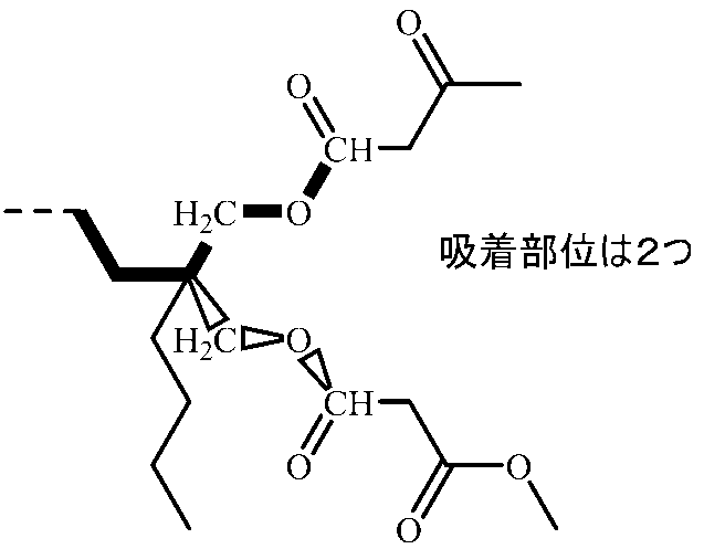
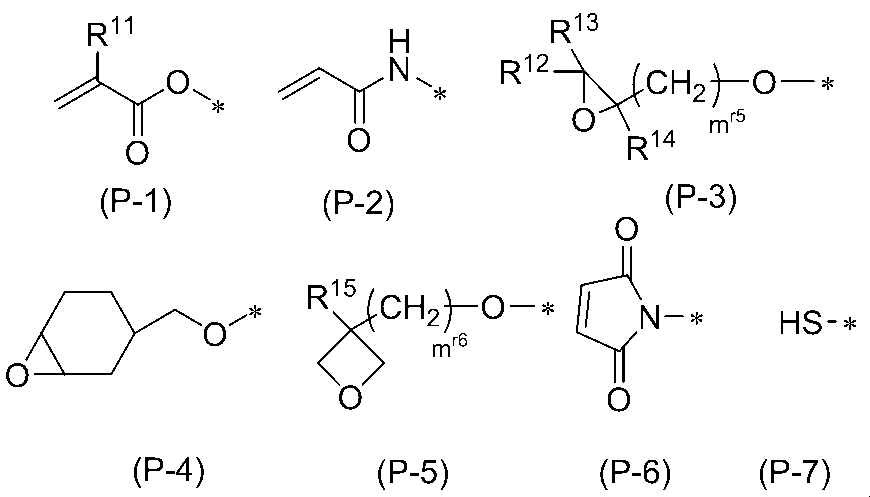
本発明に係る吸着部位の数の下限は、2以上であり、3以上が好ましく、4以上がより好ましい。本発明に係る吸着部位の数の上限は、10以下であることが好ましく、8以下であることがより好ましい。吸着部位が多すぎると液晶組成物中における配向付与化合物の相溶性が悪化し析出する。一方、吸着部位が少なすぎると基板や絶縁層に対する固定力が低減するため、表示ムラが生じる。
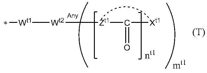
上記Rt1は、水素原子、炭素原子数1~5個のアルキル基又はZt1と結合してもよい炭素原子数1~8個の直鎖状若しくは分岐状のアルキレン基又はZt1と結合してもよい炭素原子数2~8個の直鎖状若しくは分岐状のアルケニレン基を表し、上記Zt2は、単結合、炭素原子数1~18個の直鎖状若しくは分岐状のアルキレン基又は炭素原子数2~18個の直鎖状若しくは分岐状のアルケニレン基を表し、当該アルキレン基又は当該アルケニレン基の-CH2-は酸素原子が直接隣接しないように、-COO-、-C(=O)-、-OOC-に置換されてもよく、
Zt1は、単結合、炭素原子数1~18個の直鎖状若しくは分岐状のアルキレン基又は炭素原子数2~18個の直鎖状若しくは分岐状のアルケニレン基を表し、当該アルキレン基の-CH2-は酸素原子が直接隣接しないように-O-、-COO-、-C(=O)-、-OCO-に置換されてもよく、またXt1が-Zt2-O-Rat基であり、かつRatがアルキレン基又はアルケニレン基の場合、Zt1の水素原子を置換してRt1と結合してもよく
-Wt2-Anyは、単結合又は2価~4価の有機基を表し、
-Wt1-は、単結合又は直鎖状若しくは分岐状のアルキレン基を表し、当該アルキレン基の-CH2-は酸素原子が直接隣接しないように-O-、-COO-、-C(=O)-、-OCO-に置換されてもよく、
nt1は0以上4以下の整数を表し、
mt1は1以上3以下の整数を表し、分子内の水素原子はPal-Spal-に置換されてもよく、*は結合手を表し、メソゲン基、Pal-Spal-、屈曲基又はスペーサー基と結合する。)
上記一般式(T)において、Pal-Spal-は重合性基を含む基であり、
Palは、上記式(P-1)から式(P-7)からなる群から選択される少なくとも1種を表し、Spalはスペーサー基を表す。スペーサー基は、炭素原子数1~18個の直鎖状若しくは分岐状のアルキレン基又は単結合を表し、当該アルキレン基の-CH2-は酸素原子が直接隣接しないように-O-、-COO-、-C(=O)-、-OCO-、-C=C-に置換されてもよい。
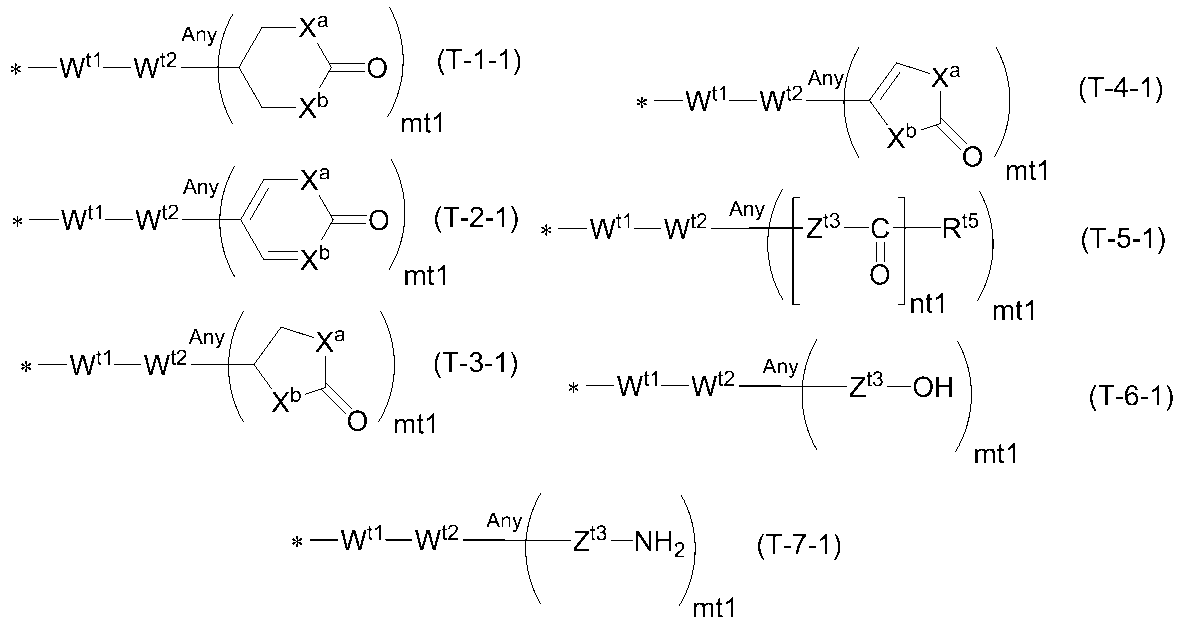
Rt5は、炭素原子数1~8個の直鎖状又は分岐状のアルキル基、シアノ化アルキル基又は炭素原子数1~8個の直鎖状又は分岐状のアルコキシ基を表し、これらのアルキル基中の少なくとも2個以上の-CH2-は酸素原子が直接隣接しないように-CH=CH-、-C≡C-、-O-又は-NH-に置換されてもよく、
Zt3は、単結合、炭素原子数1~18個の直鎖状若しくは分岐状のアルキレン基又は炭素原子数2~18個の直鎖状若しくは分岐状のアルケニレン基を表し、当該アルキレン基又は当該アルケニレン基の-CH2-は酸素原子が直接隣接しないように-O-、-COO-、-C(=O)-、-OCO-に置換されてもよく、
-Wt2-Anyは、単結合又は1価~4価の有機基を表し、
-Wt1-は、単結合又は直鎖状若しくは分岐状のアルキレン基を表し、
nt1は0以上4以下の整数を表し、
mt1は1以上3以下の整数を表し、分子内の水素原子は上記重合性基Pal-Spal-に置換されてもよく、*は結合手を表し、メソゲン基、Pal-Spal-、屈曲基又はスペーサー基と結合する。)
上記一般式(T-1-1)~(T-4-1)において、Xa又はXbのいずれかが-O-であることが好ましく、Xa及びXbが-O-であることがより好ましい。
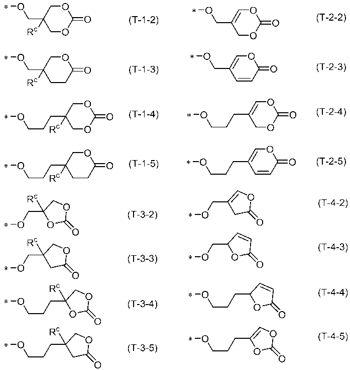
上記一般式(T-5-1)は、一般式(T-5-2)を表すことが好ましい。
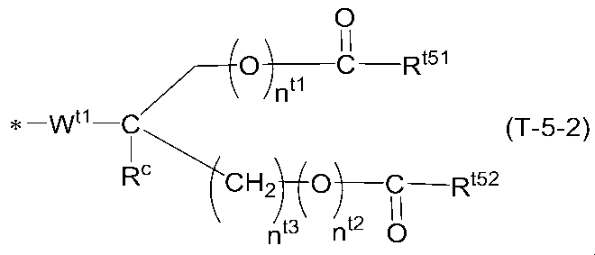
上記一般式(T-5-1)の具体例としては、以下の基が挙げられる。

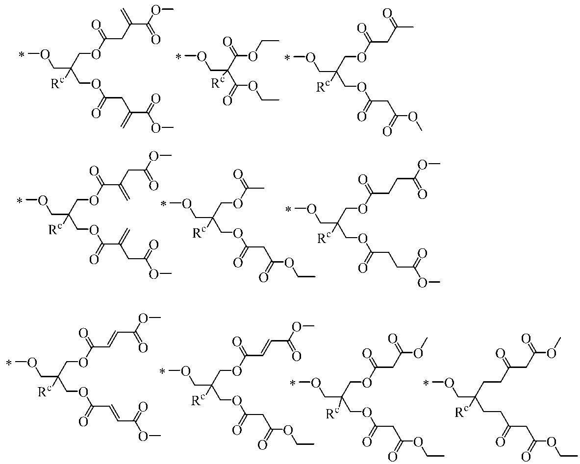
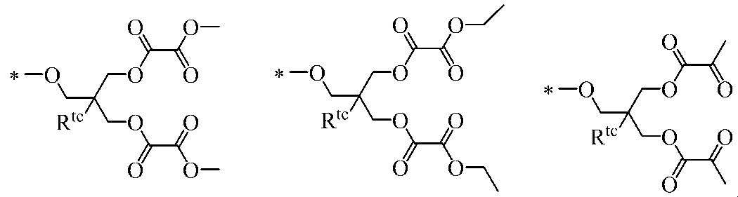


上記一般式(T-6-1)の具体例としては、以下の例が挙げられる。

上記一般式(T-7-1)の具体例としては、以下の例が挙げられる。

本発明に係る配向付与化合物において、吸着基に含まれる極性要素や重合性基に含まれる極性部分を局在化させる形態が好ましい。吸着基は液晶組成物を垂直配向させるために重要な構造であり、吸着基と重合性基とが隣接していることで、より良好な配向性が得られ、また液晶組成物への良好な溶解性を示す。具体的には、メソゲン基の同一環上に重合性基及び吸着基を有する形態が好ましい。この場合、1以上の重合性基及び1以上の吸着基が直接又はスペーサー基を介してそれぞれ同一環上に結合している形態と、1以上の重合性基の少なくとも一つ又は1以上の吸着基の少なくとも一つのうち、一方が他方に結合して、同一環上に重合性基及び吸着基を有する形態とを含む。

Xa及びXbは、-O-、-S-または-CH2-を表し、
Lt151a及びLt151aはそれぞれ独立して、メチレン基、エチレン基、プロピレン基、ビニリデン基、ビニレン基、イソプロペニレン基またはエチリデン基を表し、
nt11c、nt151c、nt16c、nt151d、nt151e、nt151f及びnt151gはそれぞれ独立して、0又は1を表し、nt11a、nt11b、nt16a、nt16b、nt151a及びnt151bはそれぞれ独立して、1~11の整数を表し、*はメソゲン基への結合手を表す。)
上記式(T-1-1.1)において、XaまたはXbのいずれか一方が-O-であることが好ましく、Xa及びXbが-O-であることがより好ましい。
nt11a、nt11b、nt16a、nt16b、nt151a及びnt151bはそれぞれ独立して、1~8の整数であることが好ましく、1~5の整数であることがより好ましい。
本発明に係る屈曲基は、液晶分子の配向を誘導する機能を有しており、直鎖状若しくは分岐状の炭素原子数1~20のアルキレン基を表すことが好ましく、直鎖状の炭素原子数1~20のアルキレン基を表すことがより好ましく、直鎖状の炭素原子数2~15のアルキレン基を表すことがより好ましい。また、当該アルキレン基中の1個又は隣接していない2個以上の-CH2-は、それぞれ独立して、-CH=CH-、-C≡C-、-O-、-CO-、-COO-又は-OCO-によって置換されていてもよい。

Lal5、Lal6、Lal7及びLal8はそれぞれ独立して、水素原子、炭素原子数1~12個のアルキル基、ハロゲン原子又は上記Pal-Spal-を表し、当該アルキル基において、1個又は隣接しない2個以上の-CH2-は、-O-又は-CH=CH-で置換されてもよく、
環Aal3は、1,4-シクロへキシレン又は1,4-フェニレンを表し、
Rala又はRalbはそれぞれ独立して、水素原子又は上記Pal-Spal-を表し、Rala又はRalbの少なくとも一つが上記Pal-Spal-を表し、
Zal3は、単結合、-CH2-CH2-、-CH2-O-又はO-CH2-を表し、
Ral4は、上記一般式(T)で表される吸着基を表し、
pal3及びpal4はそれぞれ独立して、0又は1を表す。)
上記一般式(al-1-1)において、Lal7及びLal8の一方が、炭素原子数1~5個のアルキル基を表すことが好ましい。

nL1は0、1、2又は3を表し、
AL1、AL2及びAL3はそれぞれ独立して
(a) 1,4-シクロヘキシレン基(この基中に存在する1個の-CH2-又は隣接していない2個以上の-CH2-は-O-に置き換えられてもよい。)
(b) 1,4-フェニレン基(この基中に存在する1個の-CH=又は隣接していない2個以上の-CH=は-N=に置き換えられてもよい。)及び
(c) ナフタレン-2,6-ジイル基、1,2,3,4-テトラヒドロナフタレン-2,6-ジイル基又はデカヒドロナフタレン-2,6-ジイル基(ナフタレン-2,6-ジイル基又は1,2,3,4-テトラヒドロナフタレン-2,6-ジイル基中に存在する1個の-CH=又は隣接していない2個以上の-CH=は-N=に置き換えられても良い。)
からなる群より選ばれる基を表し、上記の基(a)、基(b)及び基(c)はそれぞれ独立してシアノ基、フッ素原子又は塩素原子で置換されていても良く、
ZL1及びZL2はそれぞれ独立して単結合、-CH2CH2-、-(CH2)4-、-OCH2-、-CH2O-、-COO-、-OCO-、-OCF2-、-CF2O-、-CH=N-N=CH-、-CH=CH-、-CF=CF-又は-C≡C-を表し、
nL1が2又は3であってAL2が複数存在する場合は、それらは同一であっても異なっていても良く、nL1が2又は3であってZL2が複数存在する場合は、それらは同一であっても異なっていても良い。)
上記一般式(L)で表される化合物は、以下の式(L-1)~(L-13)で表される化合物であることが好ましい。

本発明に係る液晶組成物は非重合性液晶化合物を含み、当該非重合性液晶化合物は、第2の成分として、誘電的に正の化合物(Δεが2より大きい。)の一般式(J)で表される化合物および/または誘電的に負の化合物(Δεの符号が負で、その絶対値が2より大きい。)の一般式(N-1)~(N~3)で表される化合物を1種類又は2種類以上含有することが好ましい。

nJ1は、0、1、2、3又は4を表し、
AJ1、AJ2及びAJ3は、それぞれ独立して、
(a) 1,4-シクロヘキシレン基(この基中に存在する1個の-CH2-又は隣接していない2個以上の-CH2-は-O-に置き換えられてもよい。)
(b) 1,4-フェニレン基(この基中に存在する1個の-CH=又は隣接していない2個以上の-CH=は-N=に置き換えられてもよい。)及び
(c) ナフタレン-2,6-ジイル基、1,2,3,4-テトラヒドロナフタレン-2,6-ジイル基又はデカヒドロナフタレン-2,6-ジイル基(ナフタレン-2,6-ジイル基又は1,2,3,4-テトラヒドロナフタレン-2,6-ジイル基中に存在する1個の-CH=又は隣接していない2個以上の-CH=は-N=に置き換えられても良い。)
からなる群より選ばれる基を表し、上記の基(a)、基(b)及び基(c)はそれぞれ独立してシアノ基、フッ素原子、塩素原子、メチル基、トリフルオロメチル基又はトリフルオロメトキシ基で置換されていても良く、
ZJ1及びZJ2は、それぞれ独立して、単結合、-CH2CH2-、-(CH2)4-、-OCH2-、-CH2O-、-OCF2-、-CF2O-、-COO-、-OCO-又は-C≡C-を表し、
nJ1が2、3又は4であってAJ2が複数存在する場合は、それらは同一であっても異なっていても良く、nJ1が2、3又は4であってZJ1が複数存在する場合は、それらは同一であっても異なっていても良く、
XJ1は、水素原子、フッ素原子、塩素原子、シアノ基、トリフルオロメチル基、フルオロメトキシ基、ジフルオロメトキシ基、トリフルオロメトキシ基又は2,2,2-トリフルオロエチル基を表す。)
上記誘電的に負の化合物(Δεの符号が負で、その絶対値が2より大きい。)の一般式(N-1)~(N-3)で表される化合物からなる群から選択される1種または2種以上は、以下の通りである。

AN11、AN12、AN21、AN22、AN31及びAN32は、それぞれ独立して、
(a) 1,4-シクロヘキシレン基(この基中に存在する1個の-CH2-又は隣接していない2個以上の-CH2-は-O-に置き換えられてもよい。)
(b) 1,4-フェニレン基(この基中に存在する1個の-CH=又は隣接していない2個以上の-CH=は-N=に置き換えられてもよい。)
(c) ナフタレン-2,6-ジイル基、1,2,3,4-テトラヒドロナフタレン-2,6-ジイル基又はデカヒドロナフタレン-2,6-ジイル基(ナフタレン-2,6-ジイル基又は1,2,3,4-テトラヒドロナフタレン-2,6-ジイル基中に存在する1個の-CH=又は隣接していない2個以上の-CH=は-N=に置き換えられても良い。)及び
(d) 1,4-シクロヘキセニレン基
からなる群より選ばれる基を表し、上記の基(a)、基(b)、基(c)及び基(d)はそれぞれ独立して、シアノ基、フッ素原子又は塩素原子で置換されていても良く、
ZN11、ZN12、ZN21、ZN22、ZN31及びZN32は、それぞれ独立して、単結合、-CH2CH2-、-(CH2)4-、-OCH2-、-CH2O-、-COO-、-OCO-、-OCF2-、-CF2O-、-CH=N-N=CH-、-CH=CH-、-CF=CF-又は-C≡C-を表し、
XN21は水素原子又はフッ素原子を表し、
TN31は-CH2-又は酸素原子を表し、
nN11、nN12、nN21、nN22、nN31及びnN32はそれぞれ独立して0~3の整数を表すが、nN11+nN12、nN21+nN22及びnN31+nN32はそれぞれ独立して1、2又は3であり、AN11~AN32、ZN11~ZN32が複数存在する場合は、それらは同一であっても異なっていても良い。)
本発明に係る液晶組成物は、吸着部位を含む化合物を含み、必要によりさらに重合性化合物をさらに含有しても良い。当該重合性化合物としては、一般式(II):

S21は、単結合又は炭素数1~15のアルキレン基を表し、該アルキレン基中の1つ又は2つ以上の-CH2-は、酸素原子が直接隣接しないように、-O-、-OCO-又は-COO-で置換されてよく、
n21は、0、1又は2を表し、
A21は、
(a) 1,4-シクロヘキシレン基(この基中に存在する1個の-CH2-又は隣接していない2個以上の-CH2-は-O-に置き換えられてもよい。)
(b) 1,4-フェニレン基(この基中に存在する1個の-CH=又は隣接していない2個以上の-CH=は-N=に置き換えられてもよい。)及び
(c) ナフタレン-2,6-ジイル基、1,2,3,4-テトラヒドロナフタレン-2,6-ジイル基又はデカヒドロナフタレン-2,6-ジイル基(ナフタレン-2,6-ジイル基又は1,2,3,4-テトラヒドロナフタレン-2,6-ジイル基中に存在する1個の-CH=又は隣接していない2個以上の-CH=は-N=に置き換えられても良い。)
からなる群より選ばれる基を表し、上記の基(a)、基(b)及び基(c)は、それぞれ独立して、炭素原子数1~12のアルキル基、炭素原子数1~12のアルコキシ基、ハロゲン、シアノ基、ニトロ基又はP21-S21-で置換されていても良く、
上記一般式(II)の1分子内に少なくとも1以上のP21-S21-を有し、
L21は単結合、-OCH2-、-CH2O-、-C2H4-、-OC2H4O-、-COO-、-OCO-、-CH=CRa-COO-、-CH=CRa-OCO-、-COO-CRa=CH-、-OCO-CRa=CH-、-(CH2)z-COO-、-(CH2)z-OCO-、-OCO-(CH2)z-、-COO-(CH2)z-、-CH=CH-、-CF2O-、-OCF2-又は-C≡C-(式中、Raはそれぞれ独立して水素原子又は炭素原子数1~3のアルキル基を表し、前記式中、zはそれぞれ独立して1~4の整数を表す。)を表す。
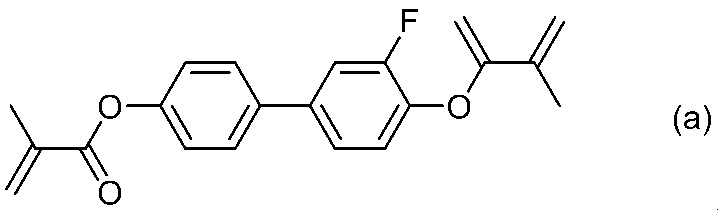


Claims (9)
- 第1の基板および前記第1の基板と対向して設けられた第2の基板と、
前記第1の基板上に設けられた第1の絶縁層および第1の電極層と、
前記第1の基板と前記第2の基板との間に設けられ、液晶分子に配向を付与する配向付与成分を含有する液晶層とを有し、
前記液晶層は、前記第1の絶縁層と相互作用を奏する吸着部位を2つ以上備える配向付与化合物を含有する液晶組成物から形成されることを特徴とする液晶表示素子。 - 前記絶縁層は、有機絶縁層または無機絶縁層である、請求項1に記載の液晶表示素子。
- 前記第2の基板上に第2の有機層および第2の電極層を有する請求項1または2に記載の液晶表示素子。
- 前記吸着部位として吸着基と重合性基とを有し、前記吸着基の数と前記重合性基の数との合計が2以上である、請求項1~3のいずれか1項に記載の液晶表示素子。
- 前記液晶層中の前記配向付与成分は、前記第1の基板表面を被覆する請求項1~4のいずれか1項に記載の液晶表示素子。
- 前記第1の電極層は、フィッシュボーン型の画素電極を有する、請求項1~5のいずれか1項に記載の液晶表示素子。
- 前記配向付与化合物は2~5個の環式基が連結したメソゲン基を有し、前記メソゲン基の長軸方向の一端の1つの前記環式基に対して前記吸着部位が連結されている、請求項1~6のいずれか1項に記載の液晶表示素子。
- 前記第1の絶縁層が有機絶縁層であり、当該有機絶縁層と前記配向付与成分とが当接している、請求項1~7のいずれか1項に記載の液晶表示素子。
- 前記配向付与化合物及び前記配向付与成分は、前記第1の基板又は前記第2の基板に対して略垂直方向の配向を前記液晶層中の液晶分子に付与する、請求項1~8のいずれか1項に記載の液晶表示素子。
Priority Applications (3)
| Application Number | Priority Date | Filing Date | Title |
|---|---|---|---|
| CN201880074635.2A CN111356952A (zh) | 2017-12-22 | 2018-12-11 | 液晶显示元件 |
| JP2019515674A JPWO2019124155A1 (ja) | 2017-12-22 | 2018-12-11 | 液晶表示素子 |
| KR1020207014405A KR20200098496A (ko) | 2017-12-22 | 2018-12-11 | 액정 표시 소자 |
Applications Claiming Priority (2)
| Application Number | Priority Date | Filing Date | Title |
|---|---|---|---|
| JP2017-246416 | 2017-12-22 | ||
| JP2017246416 | 2017-12-22 |
Publications (1)
| Publication Number | Publication Date |
|---|---|
| WO2019124155A1 true WO2019124155A1 (ja) | 2019-06-27 |
Family
ID=66994058
Family Applications (1)
| Application Number | Title | Priority Date | Filing Date |
|---|---|---|---|
| PCT/JP2018/045435 Ceased WO2019124155A1 (ja) | 2017-12-22 | 2018-12-11 | 液晶表示素子 |
Country Status (5)
| Country | Link |
|---|---|
| JP (1) | JPWO2019124155A1 (ja) |
| KR (1) | KR20200098496A (ja) |
| CN (1) | CN111356952A (ja) |
| TW (1) | TWI773854B (ja) |
| WO (1) | WO2019124155A1 (ja) |
Cited By (1)
| Publication number | Priority date | Publication date | Assignee | Title |
|---|---|---|---|---|
| WO2023149080A1 (ja) * | 2022-02-01 | 2023-08-10 | ソニーグループ株式会社 | 位相変調素子および位相変調素子の製造方法 |
Citations (3)
| Publication number | Priority date | Publication date | Assignee | Title |
|---|---|---|---|---|
| JP2003149647A (ja) * | 2001-08-31 | 2003-05-21 | Fujitsu Display Technologies Corp | 液晶表示装置及びその製造方法 |
| JP2015168826A (ja) * | 2014-03-10 | 2015-09-28 | メルク パテント ゲゼルシャフト ミット ベシュレンクテル ハフツングMerck Patent Gesellschaft mit beschraenkter Haftung | ホメオトロピック配向を有する液晶媒体 |
| WO2016114093A1 (ja) * | 2015-01-14 | 2016-07-21 | Jnc株式会社 | 重合性基を有する化合物、液晶組成物および液晶表示素子 |
Family Cites Families (3)
| Publication number | Priority date | Publication date | Assignee | Title |
|---|---|---|---|---|
| KR101779510B1 (ko) * | 2010-11-11 | 2017-09-19 | 삼성디스플레이 주식회사 | 액정 표시 장치 및 그 제조 방법 |
| KR20130092816A (ko) * | 2012-02-13 | 2013-08-21 | (주)켐넥스 | 반응성 메소젠 화합물, 이를 포함하는 액정 조성물, 표시 패널의 제조 방법 및 표시 패널 |
| US9678386B2 (en) | 2012-10-19 | 2017-06-13 | Merck Patent Gmbh | Liquid-crystal display device and process for producing liquid-crystal display device |
-
2018
- 2018-12-10 TW TW107144292A patent/TWI773854B/zh active
- 2018-12-11 CN CN201880074635.2A patent/CN111356952A/zh not_active Withdrawn
- 2018-12-11 KR KR1020207014405A patent/KR20200098496A/ko not_active Withdrawn
- 2018-12-11 WO PCT/JP2018/045435 patent/WO2019124155A1/ja not_active Ceased
- 2018-12-11 JP JP2019515674A patent/JPWO2019124155A1/ja active Pending
Patent Citations (3)
| Publication number | Priority date | Publication date | Assignee | Title |
|---|---|---|---|---|
| JP2003149647A (ja) * | 2001-08-31 | 2003-05-21 | Fujitsu Display Technologies Corp | 液晶表示装置及びその製造方法 |
| JP2015168826A (ja) * | 2014-03-10 | 2015-09-28 | メルク パテント ゲゼルシャフト ミット ベシュレンクテル ハフツングMerck Patent Gesellschaft mit beschraenkter Haftung | ホメオトロピック配向を有する液晶媒体 |
| WO2016114093A1 (ja) * | 2015-01-14 | 2016-07-21 | Jnc株式会社 | 重合性基を有する化合物、液晶組成物および液晶表示素子 |
Cited By (1)
| Publication number | Priority date | Publication date | Assignee | Title |
|---|---|---|---|---|
| WO2023149080A1 (ja) * | 2022-02-01 | 2023-08-10 | ソニーグループ株式会社 | 位相変調素子および位相変調素子の製造方法 |
Also Published As
| Publication number | Publication date |
|---|---|
| TW201930560A (zh) | 2019-08-01 |
| JPWO2019124155A1 (ja) | 2020-10-22 |
| TWI773854B (zh) | 2022-08-11 |
| KR20200098496A (ko) | 2020-08-20 |
| CN111356952A (zh) | 2020-06-30 |
Similar Documents
| Publication | Publication Date | Title |
|---|---|---|
| JP6439990B2 (ja) | 重合性液晶組成物 | |
| JP6099315B2 (ja) | 液晶表示装置及び配向膜 | |
| US8860913B2 (en) | Liquid crystal display device, method for manufacturing liquid crystal display device, composition for forming photopolymer film, and composition for forming liquid crystal layer | |
| JP6260747B2 (ja) | 液晶表示素子 | |
| JP6077222B2 (ja) | 液晶表示装置 | |
| JP5525108B2 (ja) | 液晶表示装置 | |
| US20130271713A1 (en) | Liquid crystal display device and method for manufacturing liquid crystal display device | |
| TWI854965B (zh) | 液晶組成物 | |
| JP6358489B2 (ja) | 液晶表示素子 | |
| WO2013024750A1 (ja) | 液晶表示装置 | |
| WO2013080777A1 (ja) | 液晶表示装置 | |
| JP6403037B2 (ja) | 液晶表示素子およびその製造方法 | |
| WO2013031462A1 (ja) | 液晶表示装置の製造方法 | |
| JPWO2018105439A1 (ja) | 液晶表示素子 | |
| WO2013031616A1 (ja) | 液晶表示パネル及び液晶表示装置 | |
| JP2016206445A (ja) | 液晶表示素子 | |
| KR102409741B1 (ko) | 액정표시장치 및 이의 제조방법 | |
| WO2017026478A1 (ja) | 液晶表示素子 | |
| WO2019124155A1 (ja) | 液晶表示素子 | |
| JP2018101096A (ja) | 液晶表示素子及び重合性液晶組成物 | |
| WO2018216485A1 (ja) | 液晶表示素子およびその製造方法 | |
| TW202035659A (zh) | 液晶顯示裝置 | |
| JP2020204726A (ja) | 液晶表示素子 |
Legal Events
| Date | Code | Title | Description |
|---|---|---|---|
| ENP | Entry into the national phase |
Ref document number: 2019515674 Country of ref document: JP Kind code of ref document: A |
|
| 121 | Ep: the epo has been informed by wipo that ep was designated in this application |
Ref document number: 18892855 Country of ref document: EP Kind code of ref document: A1 |
|
| ENP | Entry into the national phase |
Ref document number: 20207014405 Country of ref document: KR Kind code of ref document: A |
|
| NENP | Non-entry into the national phase |
Ref country code: DE |
|
| 122 | Ep: pct application non-entry in european phase |
Ref document number: 18892855 Country of ref document: EP Kind code of ref document: A1 |