WO2019097909A1 - 半導体素子、半導体装置および半導体素子の製造方法 - Google Patents
半導体素子、半導体装置および半導体素子の製造方法 Download PDFInfo
- Publication number
- WO2019097909A1 WO2019097909A1 PCT/JP2018/037797 JP2018037797W WO2019097909A1 WO 2019097909 A1 WO2019097909 A1 WO 2019097909A1 JP 2018037797 W JP2018037797 W JP 2018037797W WO 2019097909 A1 WO2019097909 A1 WO 2019097909A1
- Authority
- WO
- WIPO (PCT)
- Prior art keywords
- substrate
- imaging device
- imaging
- semiconductor
- semiconductor element
- Prior art date
- Legal status (The legal status is an assumption and is not a legal conclusion. Google has not performed a legal analysis and makes no representation as to the accuracy of the status listed.)
- Ceased
Links
Images





Classifications
-
- H—ELECTRICITY
- H10—SEMICONDUCTOR DEVICES; ELECTRIC SOLID-STATE DEVICES NOT OTHERWISE PROVIDED FOR
- H10W—GENERIC PACKAGES, INTERCONNECTIONS, CONNECTORS OR OTHER CONSTRUCTIONAL DETAILS OF DEVICES COVERED BY CLASS H10
- H10W72/00—Interconnections or connectors in packages
- H10W72/071—Connecting or disconnecting
-
- H—ELECTRICITY
- H10—SEMICONDUCTOR DEVICES; ELECTRIC SOLID-STATE DEVICES NOT OTHERWISE PROVIDED FOR
- H10W—GENERIC PACKAGES, INTERCONNECTIONS, CONNECTORS OR OTHER CONSTRUCTIONAL DETAILS OF DEVICES COVERED BY CLASS H10
- H10W70/00—Package substrates; Interposers; Redistribution layers [RDL]
- H10W70/60—Insulating or insulated package substrates; Interposers; Redistribution layers
- H10W70/67—Insulating or insulated package substrates; Interposers; Redistribution layers characterised by their insulating layers or insulating parts
- H10W70/68—Shapes or dispositions thereof
- H10W70/682—Shapes or dispositions thereof comprising holes having chips therein
-
- H—ELECTRICITY
- H10—SEMICONDUCTOR DEVICES; ELECTRIC SOLID-STATE DEVICES NOT OTHERWISE PROVIDED FOR
- H10W—GENERIC PACKAGES, INTERCONNECTIONS, CONNECTORS OR OTHER CONSTRUCTIONAL DETAILS OF DEVICES COVERED BY CLASS H10
- H10W72/00—Interconnections or connectors in packages
- H10W72/851—Dispositions of multiple connectors or interconnections
- H10W72/874—On different surfaces
- H10W72/884—Die-attach connectors and bond wires
-
- H—ELECTRICITY
- H10—SEMICONDUCTOR DEVICES; ELECTRIC SOLID-STATE DEVICES NOT OTHERWISE PROVIDED FOR
- H10W—GENERIC PACKAGES, INTERCONNECTIONS, CONNECTORS OR OTHER CONSTRUCTIONAL DETAILS OF DEVICES COVERED BY CLASS H10
- H10W74/00—Encapsulations, e.g. protective coatings
Definitions
- the present technology relates to a semiconductor device, a semiconductor device, and a method of manufacturing the semiconductor device.
- the present invention relates to a semiconductor device and a semiconductor device which are bonded and mounted on a substrate and a method of manufacturing the semiconductor device.
- a semiconductor device in which a semiconductor element such as a solid-state imaging element is bonded to a support substrate.
- the solid-state imaging device is a semiconductor device that generates an image signal from a subject image formed by the imaging optical system.
- it is necessary to improve the mounting accuracy to the support substrate.
- a semiconductor device is used in which a concave portion extending to the outer edge of the semiconductor element is provided on the surface of the semiconductor element to be bonded to the supporting substrate, and an adhesive is disposed in this concave portion to bond to the supporting substrate. 1)).
- the semiconductor element is mounted on a supporting substrate by bonding the semiconductor element to a supporting substrate, and the semiconductor device is configured.
- the semiconductor device after mounting causes deflection due to the influence of heat. This is because the thermal expansion coefficients of the semiconductor element and the support substrate are different, so that expansion and contraction of the semiconductor element and the support substrate become uneven when heating and cooling are performed in mounting. Therefore, there is a problem that the semiconductor element is warped and the mounting accuracy is lowered.
- the present technology has been made in view of the above-described problems, and aims to improve the mounting accuracy of the semiconductor element after mounting.
- a first side surface of the present technology is a semiconductor element provided with a recess that adjusts a warp when it is bonded and mounted on a substrate.
- the rigidity of the semiconductor element is adjusted by the recess, and the warpage of the semiconductor element when mounted on the substrate is adjusted.
- the concave portion may adjust the warpage when it is joined and mounted to the substrate sealed in the sealing portion. This brings about the effect
- the concave portion may adjust a warp when a semiconductor package in which a substrate to which its own semiconductor element is bonded is disposed is bonded and mounted to a second substrate. This brings about the effect that the warpage when the semiconductor package in which the substrate to which the semiconductor element is joined is disposed is joined and mounted to the second substrate is adjusted by the recess. Adjustment of warpage of the semiconductor element on the second substrate on which the semiconductor package is mounted is assumed.
- the recess may be disposed in a region different from the end of its own semiconductor element. This brings about the effect
- a second aspect of the present technology seals a substrate, a semiconductor element including a recess for adjusting a warp when being bonded and mounted on the substrate, and the substrate on which the semiconductor element is mounted. And a sealing portion.
- the third aspect of the present technology also includes the semiconductor element including the semiconductor element including the recess for adjusting the warpage when the semiconductor package on which the substrate to which the semiconductor element is bonded is disposed is mounted.
- a semiconductor device including a second substrate on which a semiconductor package having a substrate disposed thereon is joined and mounted. This brings about the effect that the warpage when the semiconductor package in which the substrate to which the semiconductor element is joined is disposed is joined and mounted to the second substrate is adjusted by the recess. Adjustment of warpage of the semiconductor element on the second substrate on which the semiconductor package is mounted is assumed.
- the 4th side surface of this technique is based on the curvature which measured the curvature measurement process which measures curvature of its own semiconductor element, and the recessed part which adjusts the curvature at the time of being joined and mounted to a board
- the excellent effect of improving the mounting accuracy of the semiconductor element after mounting is exhibited.
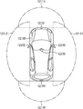
- FIG. 1 is a cross-sectional view showing a configuration example of a solid-state imaging device to which the present technology can be applied. It is a block diagram showing an example of rough composition of a camera which is an example of an imaging device to which this art can be applied. It is a figure which shows an example of a schematic structure of an endoscopic surgery system. It is a block diagram which shows an example of a function structure of a camera head and CCU. It is a block diagram showing an example of rough composition of a vehicle control system. It is explanatory drawing which shows an example of the installation position of a vehicle exterior information detection part and an imaging part.
- FIG. 1 is a diagram illustrating a configuration example of an imaging device according to an embodiment of the present technology.
- the imaging device 10 of the figure represents an example of an imaging device in which an imaging element is mounted and configured in a semiconductor package.
- the configuration of the imaging device 10 will be described by taking this semiconductor package as an example.
- a is a view showing the appearance of the imaging device 10
- b in the figure is a cross-sectional view showing the configuration of the imaging device 10.
- the imaging device 10 of FIG. 1 includes an imaging element 1, a substrate 3, a frame 4, and a seal glass 5.
- the imaging device 10 is an example of the semiconductor device described in the claims.
- the imaging device 1 is an example of the semiconductor device described in the claims.
- the imaging device 1 is a semiconductor device that converts light from an illuminated subject into an image signal.
- pixels for performing photoelectric conversion according to the irradiated light an on-chip lens arranged for each pixel to condense the irradiated light on the pixels, and light of a desired wavelength for the pixels A color filter or the like for incidence is arranged.
- the recess 2 is disposed on the back surface of the imaging device 1.
- a surface on which a diffusion region or the like of a circuit component to be incorporated corresponds to the surface.
- the surface on which the region for mainly mechanically supporting the semiconductor element is disposed corresponds to the back surface.
- the surface different from the surface on which the diffusion region and the like according to the circuit component are formed corresponds to the back surface.
- the back surface corresponds to the surface on the side of the supporting substrate which is a substrate for supporting the semiconductor elements.
- the surface on which the pixels and the like are arranged and the light from the subject is irradiated corresponds to the surface. It is a surface different from the said surface, and the surface where a support substrate etc. are arrange
- positioned corresponds to a back surface. Details of the configuration of the imaging device 1 will be described later.
- the substrate 3 is a substrate on which the imaging device 1 is mounted.
- an interposer corresponds to the substrate 3.
- the interposer is a substrate on which a chip-shaped semiconductor element is mounted in the semiconductor package.
- the imaging device 1 is bonded to the substrate 3 by an adhesive 7.
- the adhesive 7 may be a thermosetting adhesive, for example, an adhesive in which particles of silver are dispersed.
- the process of mounting the imaging device 1 on the substrate 3 is referred to as die bonding.
- the imaging element 1 is mechanically connected to the substrate 3 by this die bonding.
- the substrate 3 is configured by laminating a wiring layer for transmitting a signal or the like and an insulating layer for insulating the wiring layer in multiple layers.
- the wiring layer disposed on the surface of the substrate 3 and the imaging element 1 are electrically connected.
- the wiring layers of the imaging device 1 and the substrate 3 are electrically connected by the bonding wires 8.
- the bonding wire 8 is made of, for example, a gold (Au) wire, and is connected to pads formed on the imaging device 1 and the substrate 3 to make an electrical connection.
- the pad is a region in which a conductor for exchanging an electrical signal with an external substrate or the like in the imaging device 1 or the like is disposed. This pad is connected to the wiring layer.
- the process of connecting the bonding wires 8 to the pads of the imaging device 1 and the substrate 3 is referred to as wire bonding.
- a substrate having an insulating layer formed of ceramic can be used.
- a substrate on which an insulating layer is formed of a resin can be used.
- Solder bumps 6 are formed on the bottom surface (back surface) of the substrate 3.
- the solder bumps 6 are connected to the wiring layer of the substrate 3 to transmit signals.
- the signal of the imaging device 1 is exchanged with the outside of the semiconductor package through the substrate 3 and the solder bumps 6.
- a plurality of solder bumps 6 are disposed on the back surface of the substrate 3 to transmit signals.
- the frame 4 and the seal glass 5 seal the imaging device 1.
- the frame 4 is a frame that encloses the side surface of the imaging device 1.
- the seal glass 5 is a glass plate surrounding the upper portion of the imaging device 1. Light from a subject is incident on the imaging device 1 through the seal glass 5.
- the imaging element 1 is shielded from the outside air and protected by the frame 4 and the seal glass 5.
- the frame 4 and the seal glass 5 are an example of the sealing portion described in the claims.
- the imaging device 10 configured in this way is mounted on a substrate such as a mother substrate along with other electronic components, and is used for a single-lens reflex camera or the like.
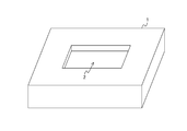
- FIG. 2 is a diagram showing a configuration example of an imaging device according to an embodiment of the present technology.
- the figure is a figure showing the appearance of the back surface of the imaging device 1.
- the recess 2 is disposed on the back surface of the imaging device 1.
- the recess 2 has an opening having a rectangular shape similar to the outer shape of the imaging device 1 and is formed to a predetermined depth.
- the rigidity of the imaging device 1 can be changed by the recess 2. Specifically, the rigidity of the imaging device 1 can be reduced by increasing the area of the opening of the recess 2 and the depth of the recess 2 from the back surface of the imaging device 1.
- the imaging device 1 is mounted on the substrate 3 and configured in a semiconductor package.
- the thermal expansion coefficients of the substrate 3 and the like constituting the semiconductor package and the imaging device 1 are different, a stress is generated due to a temperature change, and the semiconductor package is deformed.
- the imaging device 1 and the substrate 3 are heated to the curing temperature (for example, 150 ° C.) of the adhesive 7.
- the imaging device 1 and the substrate 3 are bent according to the difference in thermal expansion coefficient.
- the thermal expansion coefficient of the substrate 3 is higher than that of the imaging device 1, stress is generated in the imaging device 1 and the substrate 3 in the direction in which a convex portion is formed upward in b in FIG. For this reason, the image pickup element 1 is bent in the direction of the stress, that is, in the image pickup element 1, a convex-shaped warp is generated upward.
- Such warpage of the imaging device 1 causes an error in the surface position of the imaging device 1 and causes a reduction in the mounting accuracy of the imaging device 1.
- light from the subject is collected by an optical system member such as an imaging lens disposed outside, and an image is formed on the surface of the imaging element 1. That is, the surface of the imaging element 1 is at the focal position of the imaging lens or the like.
- the focal position shifts. The blurred image is formed on the image sensor 1, and the image quality of the image signal converted by the image sensor 1 is degraded.
- warpage also occurs in the imaging device 1 before being mounted on the substrate 3. This is because stress is generated by forming a diffusion region on the surface of the imaging device 1, laminating an upper layer film such as a color filter, and an on-chip lens in the manufacturing process of the imaging device 1.
- the imaging element 1 in which such warpage is generated in advance is mounted on the substrate 3, the imaging element 1 and the substrate 3 are generated by the stress that the imaging element 1 had and the stress caused by mounting on the substrate 3. Influence each other, deform and become in equilibrium. Therefore, by offsetting the stress applied to the imaging device 1 before and after mounting on the substrate 3, the occurrence of warpage of the imaging device can be reduced. That is, when the direction of warpage generated in the imaging device 1 before mounting on the substrate 3 is different from the direction of warpage generated in mounting the imaging device 1 on the substrate 3, stress applied to the imaging device 1 Is canceled and the warp of the imaging device 1 is reduced.
- the warpage of the imaging device 1 after being mounted on the substrate 3 can be adjusted. This is because the force relationship between the imaging device 1 and the substrate 3 in which the respective stresses described above are in equilibrium changes. For example, by reducing the rigidity of the imaging device 1, the influence of the stress from the substrate 3 or the like becomes large, and the change of the shape of the imaging device 1 by the substrate 3 is promoted. As a result, the warpage of the imaging device 1 is alleviated.
- the rigidity of the imaging device 1 can be adjusted by forming the recess 2 in the imaging device 1.
- the rigidity of the imaging device 1 is adjusted while maintaining the optical path length between the surface of the imaging device 1 and the imaging lens or the like by forming the recess 2 in the imaging device 1 and partially changing the thickness of the imaging device 1 be able to. Thereby, it is possible to adjust the warp of the imaging device 1 after being mounted on the substrate 3 or the like, and to improve the mounting accuracy of the imaging device 1.
- the surface of the imaging device 1 and the semiconductor package are adjusted when the warp of the imaging device 1 is adjusted.
- the optical path length between the seal glass 5 and the seal glass 5 is changed. That is, the optical path length between the surface of the imaging device 1 and the imaging lens or the like changes, and the image quality of the image signal converted by the imaging device 1 decreases.
- the semiconductor device can also be configured in a state in which the imaging element 1 is warped. For example, in the case of reducing the warpage of the imaging device 1 by canceling the stress applied to the imaging device 1 when the imaging device 10 is mounted on another substrate, the imaging device 1 is made to have a desired warpage.
- the image pickup apparatus 10 is mounted.
- the recess 2 in the same figure can be disposed in an area where the opening is different from the peripheral part of the imaging device 1. Thereby, the fall of the intensity
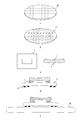
- FIG. 3 is a diagram illustrating an example of a manufacturing process of the imaging device according to the embodiment of the present technology.
- the figure is a figure showing the process at the time of manufacturing the image pick-up element 1 and the imaging device 10.
- the final product form of the imaging device 10 is mounted on a mother substrate such as a single-lens reflex camera.
- the imaging element 1 is formed on the wafer 20 (a in the same figure). Note that dotted lines a and b in the same figure indicate boundaries of a plurality of imaging elements 1.
- the concave portion 2 is formed for each of the imaging elements 1 formed on the wafer 20, and the warpage is adjusted.
- the recess 2 can be formed by dry etching such as plasma etching, wet etching using a chemical solution, mechanical grinding or the like (b in the same figure).
- dicing is performed to cut out the individual imaging elements 1 from the wafer 20 (c in the figure).
- c in the figure is a figure showing the shape of the back surface and cross section of the image pick-up element 1 after dicing, and the case where curvature arises in the direction represented to the cross section of c in the figure is assumed.
- the adhesive 7 is applied to the area of the substrate 3 on which the imaging device 1 is mounted.
- the adhesive 7 can be applied to the positions corresponding to the four sides of the imaging device 1.
- the imaging device 1 is mounted on the substrate 3 to which the adhesive 7 is applied, and the adhesive 7 is cured by heating. Thereby, the imaging device 1 is bonded and mounted on the substrate 3 (d in the same figure). At the time of this mounting, the warp of the imaging device 1 is alleviated by the deflection of the substrate 3.
- the frame 4 and the seal glass 5 are disposed on the substrate 3 on which the imaging element 1 is mounted, and the imaging device 10 is configured. Thereafter, the imaging device 10 is mounted on the substrate 30 which is a mother substrate (e in the same drawing).
- the substrate 30 is a substrate on which the imaging device 10 and other electronic components are mounted.
- the mounting of the imaging device 10 on the substrate 30 is performed by solder connection.
- the imaging device 10 is mounted on the substrate 30 by aligning the pads disposed on the substrate 30 with the solder bumps 6, and reflow soldering is performed to bond the imaging device 10 and the substrate 30. Ru.
- the warpage of the imaging device 1 is further alleviated by the deflection of the substrate 30, and it can be made into a substantially flat shape.
- the substrate 30 is an example of a second substrate described in the claims.
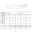
- FIG. 4 is a view showing an example of the relationship between the shape of the recess and the warp according to the embodiment of the present technology.
- a in the same figure is a figure showing the curvature amount of the image pick-up element 1.
- difference "A" of the perpendicular direction of image sensor 1 in a center part and an end corresponds to amount of curvature.
- A” assumes a positive value.
- the measurement of the amount of warpage can be performed, for example, by a three-dimensional measuring machine.
- B in the same figure is a diagram showing the relationship between the state of the imaging device 1 and the amount of warpage, the amount of warpage in the single imaging device 1 after dicing and the amount of warpage in the imaging device 1 after die bonding It is a figure showing change. Under the present circumstances, the magnitude
- the size of the imaging element 1 is 31 mm long ⁇ 40 mm wide ⁇ 0.6 mm thick. Further, the size of the opening of the recess 2 formed in the imaging device 1 is 11 mm long ⁇ 21 mm wide.
- the thicknesses of the substrate 3 and the seal glass 5 in the imaging device 10 on which the imaging device 1 b in FIG. 2 is mounted are 0.8 mm and 0.7 mm, respectively.
- the amount of warpage A of the imaging device 1 in a state in which the concave portion 2 is not formed is 10.5 ⁇ m, and the amount of warpage A changes to 3.2 ⁇ m by performing die bonding. This is because the warp of the imaging device 1 is corrected by the deflection of the substrate 3.
- the concave portion 2 is formed in such an imaging element 1 to adjust the warpage after die bonding.
- the amount of warpage after die bonding when the depth of the recess 2 is changed to 0.1 mm, 0.2 mm and 0.3 mm changes to 1.4 ⁇ m, -0.2 ⁇ m and -1.5 ⁇ m, respectively.
- the change in the amount of warpage of b in the same figure is a value representing the amount of change with respect to the amount of warpage A of the imaging device 1 when the recess 2 is not formed.
- the cross-sectional shape of b in the same figure is a figure which represented typically the shape of the cross section of the image pick-up element 1 and the board
- b in the figure by changing the depth of the recess 2, it is possible to change the shape of the warpage of the imaging device 1 after die bonding downward, substantially flat, and upward.
- the warp of the imaging device 1 when mounted on the substrate 3 can be adjusted.
- b in the same figure represents the relationship between the size of the recess 2 and the warpage of the imaging device 1 after mounting when the warpage of the imaging device 1 is 10.5 ⁇ m before the depression 2 is formed. is there.
- any warpage can be obtained by examining the relationship between the size of the recess 2 and the amount of warpage of the imaging device 1 after mounting. It is possible to adjust the warpage of the imaging device 1 having the
- the form of the final product is different by examining the relationship between the size of the recess 2 and the warp of the imaging device 1 after mounting under different conditions such as soldering to a mother substrate (substrate 30) Even in this case, the size of the necessary recess 2 can be detected.
- the concave portion 2 of the detected size in the imaging device 1 it becomes possible to manufacture a product on which the imaging device 1 having a desired warp is mounted.
- the warpage of the imaging element 1 after dicing may be detected by measuring the warpage of the wafer 20 before dicing. For example, the relationship between the warpage of the wafer 20 and the warpage of the chip (imaging element 1) after dicing according to the position of the wafer 20 is detected in advance, and the warpage of the imaging element 1 after dicing is estimated using this relation. Thereby, the warp of the imaging device 1 can be detected.
- FIG. 5 is a diagram illustrating an example of a method of manufacturing an imaging device according to the embodiment of the present technology.
- the back surface of the wafer 20 on which the diffusion region, the wiring layer and the like are formed is ground (step S100). This is because the imaging device 1 is configured to have a predetermined thickness and dicing is easily performed.
- warpage of the wafer 20 is measured (step S101). Warpage of the wafer 20 can be measured, for example, by a three-dimensional measuring device.
- the warpage of each imaging element 1 after dicing is estimated according to the measured warpage of the wafer 20.
- the size of the recess 2 is detected (step S102). This can be performed by acquiring in advance the relationship between the warpage of each of the imaging devices 1 formed on the wafer 20 and the warpage of the imaging device 1 after mounting, and detecting the size of the recess 2 based on this relationship. it can.
- the recess 2 is formed in the imaging element 1 (step S103). This can be performed by forming the recess 2 in the imaging device 1 in the wafer 20 based on the size of the recess 2 detected in step S102.
- dicing is performed (step S104). Thus, the imaging device 1 is cut out of the wafer 20.
- die bonding is performed (step S105). Thus, the imaging device 1 is mounted on the substrate 3.
- wire bonding is performed (step S106).
- the frame 4 and the seal glass 5 are disposed on the substrate 3 and sealing is performed (step S107). Thereby, the imaging device 1 can be manufactured, and the imaging device 10 in which the imaging device 1 is mounted can be manufactured.
- the concave portion in the semiconductor element by forming the concave portion in the semiconductor element, it is possible to adjust the warpage of the semiconductor element when the semiconductor element is mounted, and improve the attachment accuracy of the semiconductor element in the semiconductor device. It can be done.
- the imaging element 1 of the above-mentioned embodiment was provided with the recessed part 2 of rectangular shape, it can also be made the recessed part of a different shape. Also in the implementation form of the imaging device 10, an implementation form different from the above-described embodiment can be adopted.
- FIG. 6 is a diagram showing a configuration example of an imaging device according to a modification of the embodiment of the present technology.
- “A” in the same figure represents an example in which a rectangular groove is formed as the recess 2.
- the number of grooves can be changed according to the adjustment amount of warpage.
- b in the same figure is a figure showing the example where the some recessed part which has a circular-shaped opening part is comprised as the recessed part 2.
- the number and the arrangement position of the concave portions can be changed according to the adjustment amount of the warpage.
- FIG. 7 is a view showing a configuration example of a semiconductor device according to a modification of the embodiment of the present technology.
- a in the same figure is a figure showing the example of the imaging device 10 in case the board
- the substrate 3 of a in the figure can be made of, for example, a ceramic having a recess.
- FIG. B in the same figure is a figure showing the example of the semiconductor device 40 which abbreviate
- FIG. In applications other than the imaging device, a semiconductor package simplified using the mold resin 9 can be applied as in the semiconductor device 40. In addition, by using a transparent resin as the mold resin 9, it is possible to apply to a simple imaging device.
- the mold resin 9 is an example of the sealing portion in the claims.
- the configurations of the imaging device and the semiconductor device other than this are the same as the configurations of the imaging device and the semiconductor device described in the embodiment of the present technology, and thus the description thereof will be omitted.
- the mounting accuracy of the semiconductor element in the semiconductor device is improved by adjusting the warpage of the semiconductor element when the semiconductor element is mounted by forming the recess in the semiconductor element.
- FIG. 8 is a cross-sectional view showing a configuration example of a solid-state imaging device to which the technology according to the present disclosure can be applied.
- a PD (photodiode) 20019 receives incident light 20001 incident from the back surface (upper surface in the drawing) side of the semiconductor substrate 20018.
- a planarization film 20013, a CF (color filter) 20012, and a microlens 20011 are provided above the PD 20019, and the light receiving surface 20017 receives incident light 20001 sequentially incident through the respective parts to perform photoelectric conversion. It will be.
- the n-type semiconductor region 20000 is formed as a charge storage region for storing charges (electrons).
- the n-type semiconductor region 20020 is provided inside the p-type semiconductor regions 20016 and 20041 of the semiconductor substrate 20018.
- a p-type semiconductor region 20041 having a higher impurity concentration than the back surface (upper surface) side is provided.
- the PD 20019 has a hole-accumulation diode (HAD) structure, and a p-type semiconductor is formed to suppress generation of dark current at each interface between the upper surface side and the lower surface side of the n-type semiconductor region 20020. Regions 20016 and 20041 are formed.
- HAD hole-accumulation diode
- a pixel separation portion 20030 that electrically separates the plurality of pixels 20010 is provided, and in the region divided by the pixel separation portion 20030, a PD 20019 is provided.
- the pixel separation unit 20030 is formed in a lattice shape so as to be interposed between a plurality of pixels 20010, for example. It is formed in the area divided by.
- each PD 20019 the anode is grounded, and in the solid-state imaging device, the signal charge (for example, electrons) stored in the PD 20019 is read out through a transfer transistor (MOS FET) or the like (not shown) and is used as an electrical signal It is output to VSL (vertical signal line) not shown.
- MOS FET transfer transistor
- the wiring layer 20050 is provided on the surface (lower surface) of the semiconductor substrate 20018 opposite to the back surface (upper surface) provided with the light shielding film 20014, the CF 20012, the microlens 20011, and the like.
- the wiring layer 20050 includes a wiring 20051 and an insulating layer 20052, and in the insulating layer 20052, the wiring 20051 is formed to be electrically connected to each element.
- the wiring layer 20050 is a layer of a so-called multilayer wiring, and is formed by alternately laminating an interlayer insulating film forming the insulating layer 20052 and the wiring 20051 a plurality of times.
- a wiring for reading a charge from the PD 20019 such as a transfer transistor or a wiring for VSL or the like is stacked via the insulating layer 20052.
- a supporting substrate 20061 is provided on the surface of the wiring layer 20050 opposite to the side on which the PD 20019 is provided.
- a substrate made of a silicon semiconductor with a thickness of several hundred ⁇ m is provided as the supporting substrate 20061.
- the light shielding film 20014 is provided on the side of the back surface (upper surface in the drawing) of the semiconductor substrate 20018.
- the light shielding film 20014 is configured to shield a part of the incident light 20001 directed from the upper side of the semiconductor substrate 20018 to the back surface of the semiconductor substrate 20018.
- the light shielding film 20014 is provided above the pixel separating portion 20030 provided inside the semiconductor substrate 20018.
- the light shielding film 20014 is provided so as to protrude in a convex shape on the back surface (upper surface) of the semiconductor substrate 20018 via the insulating film 20015 such as a silicon oxide film.
- the light shielding film 20014 is not provided but opened so that the incident light 20001 is incident on the PD 20019 above the PD 20019 provided inside the semiconductor substrate 20018.
- the planar shape of the light shielding film 20014 is lattice-like, and an opening through which incident light 20001 passes to the light receiving surface 20017 is formed.
- the light shielding film 20014 is formed of a light shielding material that shields light.
- the light shielding film 20014 is formed by sequentially stacking a titanium (Ti) film and a tungsten (W) film.
- the light shielding film 20014 can be formed, for example, by sequentially laminating a titanium nitride (TiN) film and a tungsten (W) film.
- the light shielding film 20014 is covered with a planarization film 20013.
- the planarization film 20013 is formed using an insulating material which transmits light.
- the pixel separating unit 20030 includes a groove 20031, a fixed charge film 20032, and an insulating film 20033.
- the fixed charge film 20032 is formed on the side of the back surface (upper surface) of the semiconductor substrate 20018 so as to cover the groove portion 20031 partitioning the plurality of pixels 20010.
- fixed charge film 20032 is provided to cover the inner surface of groove portion 20031 formed on the back surface (upper surface) side in semiconductor substrate 20018 with a constant thickness.
- an insulating film 20033 is provided (filled) so as to fill the inside of the groove portion 20031 covered with the fixed charge film 20032.
- the fixed charge film 20032 uses a high dielectric material having a negative fixed charge so that a positive charge (hole) storage region is formed at the interface with the semiconductor substrate 20018 and generation of dark current is suppressed. It is formed. Since the fixed charge film 20032 is formed to have negative fixed charge, an electric field is applied to the interface with the semiconductor substrate 20018 by the negative fixed charge, and a positive charge (hole) storage region is formed.
- the fixed charge film 20032 can be formed of, for example, a hafnium oxide film (HfO 2 film).
- the fixed charge film 20032 can be formed to include at least one of other oxides such as hafnium, zirconium, aluminum, tantalum, titanium, magnesium, yttrium, and lanthanoid elements.
- the present technology can be applied to the solid-state imaging device as described above. Specifically, the warpage of the solid-state imaging device can be adjusted by forming the concave portion in the above-described support substrate 20061.
- the present technology can be applied to various products.
- the present technology may be realized as an imaging element mounted in an imaging device such as a camera.
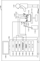
- FIG. 9 is a block diagram showing a schematic configuration example of a camera which is an example of an imaging device to which the present technology can be applied.
- the camera 1000 in this figure includes a lens 1001, an imaging element 1002, an imaging control unit 1003, a lens driving unit 1004, an image processing unit 1005, an operation input unit 1006, a frame memory 1007, and a display unit 1008. And a recording unit 1009.
- a lens 1001 is a photographing lens of the camera 1000.
- the lens 1001 condenses light from a subject and causes the light to be incident on an image sensor 1002 described later to form an image of the subject.
- the imaging element 1002 is a semiconductor element that captures light from an object collected by the lens 1001.
- the imaging element 1002 generates an analog image signal according to the irradiated light, converts it into a digital image signal, and outputs it.
- the imaging control unit 1003 controls imaging in the imaging element 1002.
- the imaging control unit 1003 controls the imaging element 1002 by generating a control signal and outputting the control signal to the imaging element 1002.
- the imaging control unit 1003 can perform autofocus in the camera 1000 based on the image signal output from the imaging element 1002.
- the autofocus is a system that detects the focal position of the lens 1001 and automatically adjusts it.
- a method image plane phase difference autofocusing
- a method detecting the image plane phase difference by the phase difference pixels arranged in the imaging element 1002 and detecting the focal position
- a method (contrast autofocus) of detecting a position at which the contrast of the image is the highest as the focus position can also be applied.
- the imaging control unit 1003 adjusts the position of the lens 1001 via the lens driving unit 1004 based on the detected focus position, and performs autofocus.
- the imaging control unit 1003 can be configured, for example, by a DSP (Digital Signal Processor) on which firmware is installed.
- DSP Digital Signal Processor
- the lens driving unit 1004 drives the lens 1001 based on the control of the imaging control unit 1003.
- the lens drive unit 1004 can drive the lens 1001 by changing the position of the lens 1001 using a built-in motor.
- An image processing unit 1005 processes an image signal generated by the image sensor 1002. This processing includes, for example, demosaicing that generates an image signal of insufficient color among image signals corresponding to red, green and blue for each pixel, noise reduction that removes noise of the image signal, encoding of the image signal, etc. Applicable
- the image processing unit 1005 can be configured, for example, by a microcomputer equipped with firmware.
- the operation input unit 1006 receives an operation input from the user of the camera 1000.
- a push button or a touch panel can be used as the operation input unit 1006.
- the operation input received by the operation input unit 1006 is transmitted to the imaging control unit 1003 and the image processing unit 1005. Thereafter, a process according to the operation input, for example, a process of imaging a subject is activated.
- the frame memory 1007 is a memory for storing a frame which is an image signal for one screen.
- the frame memory 1007 is controlled by the image processing unit 1005 and holds a frame in the process of image processing.
- the display unit 1008 displays an image processed by the image processing unit 1005.
- a liquid crystal panel can be used for the display portion 1008.
- the recording unit 1009 records an image processed by the image processing unit 1005.
- a memory card or a hard disk can be used for the recording unit 1009.
- the present technology may be applied to the imaging element 1002 among the configurations described above.
- the imaging device 10 described in FIG. 1 can be applied to the imaging element 1002.
- the image processing unit 1005 is an example of the processing circuit described in the claims.
- the camera 1000 is an example of an imaging device described in the claims.
- the technology according to the present disclosure (the present technology) can be applied to various products.
- the technology according to the present disclosure may be applied to an endoscopic surgery system.
- FIG. 10 is a diagram showing an example of a schematic configuration of an endoscopic surgery system to which the technology (the present technology) according to the present disclosure can be applied.
- the endoscopic surgery system 11000 includes an endoscope 11100, other surgical instruments 11110 such as an insufflation tube 11111 and an energy treatment instrument 11112, and a support arm device 11120 for supporting the endoscope 11100.
- a cart 11200 on which various devices for endoscopic surgery are mounted.
- the endoscope 11100 includes a lens barrel 11101 whose region of a predetermined length from the tip is inserted into a body cavity of a patient 11132, and a camera head 11102 connected to a proximal end of the lens barrel 11101.
- the endoscope 11100 configured as a so-called rigid endoscope having a rigid barrel 11101 is illustrated, but even if the endoscope 11100 is configured as a so-called flexible mirror having a flexible barrel Good.
- the endoscope 11100 may be a straight endoscope, or may be a oblique endoscope or a side endoscope.
- An optical system and an imaging device are provided inside the camera head 11102, and the reflected light (observation light) from the observation target is condensed on the imaging device by the optical system.
- the observation light is photoelectrically converted by the imaging element to generate an electric signal corresponding to the observation light, that is, an image signal corresponding to the observation image.
- the image signal is transmitted as RAW data to a camera control unit (CCU: Camera Control Unit) 11201.
- CCU Camera Control Unit
- the CCU 11201 is configured by a CPU (Central Processing Unit), a GPU (Graphics Processing Unit), and the like, and centrally controls the operations of the endoscope 11100 and the display device 11202. Furthermore, the CCU 11201 receives an image signal from the camera head 11102 and performs various image processing for displaying an image based on the image signal, such as development processing (demosaicing processing), on the image signal.
- a CPU Central Processing Unit
- GPU Graphics Processing Unit
- the display device 11202 displays an image based on an image signal subjected to image processing by the CCU 11201 under control of the CCU 11201.
- the light source device 11203 includes, for example, a light source such as a light emitting diode (LED), and supplies the endoscope 11100 with irradiation light at the time of imaging a surgical site or the like.
- a light source such as a light emitting diode (LED)
- LED light emitting diode
- the input device 11204 is an input interface to the endoscopic surgery system 11000.
- the user can input various information and input instructions to the endoscopic surgery system 11000 via the input device 11204.
- the user inputs an instruction to change the imaging condition (type of irradiated light, magnification, focal length, and the like) by the endoscope 11100, and the like.
- the treatment tool control device 11205 controls the drive of the energy treatment tool 11112 for ablation of tissue, incision, sealing of a blood vessel, and the like.
- the insufflation apparatus 11206 is a gas within the body cavity via the insufflation tube 11111 in order to expand the body cavity of the patient 11132 for the purpose of securing a visual field by the endoscope 11100 and securing a working space of the operator.
- Send The recorder 11207 is a device capable of recording various types of information regarding surgery.
- the printer 11208 is an apparatus capable of printing various types of information regarding surgery in various types such as text, images, and graphs.
- the light source device 11203 that supplies the irradiation light when imaging the surgical site to the endoscope 11100 can be configured of, for example, an LED, a laser light source, or a white light source configured by a combination of these.
- a white light source is configured by a combination of RGB laser light sources
- the output intensity and output timing of each color (each wavelength) can be controlled with high precision. It can be carried out.
- the laser light from each of the RGB laser light sources is irradiated to the observation target in time division, and the drive of the image pickup element of the camera head 11102 is controlled in synchronization with the irradiation timing to cope with each of RGB. It is also possible to capture a shot image in time division. According to the method, a color image can be obtained without providing a color filter in the imaging device.
- the drive of the light source device 11203 may be controlled so as to change the intensity of the light to be output every predetermined time.
- the drive of the imaging device of the camera head 11102 is controlled in synchronization with the timing of the change of the light intensity to acquire images in time division, and by combining the images, high dynamic without so-called blackout and whiteout is obtained. An image of the range can be generated.
- the light source device 11203 may be configured to be able to supply light of a predetermined wavelength band corresponding to special light observation.
- special light observation for example, the mucous membrane surface layer is irradiated by irradiating narrow band light as compared with irradiation light (that is, white light) at the time of normal observation using the wavelength dependency of light absorption in body tissue.
- the so-called narrow band imaging is performed to image a predetermined tissue such as a blood vessel with high contrast.
- fluorescence observation may be performed in which an image is obtained by fluorescence generated by irradiation with excitation light.
- body tissue is irradiated with excitation light and fluorescence from the body tissue is observed (autofluorescence observation), or a reagent such as indocyanine green (ICG) is locally injected into body tissue and the body tissue is Excitation light corresponding to the fluorescence wavelength of the reagent can be irradiated to obtain a fluorescence image or the like.
- the light source device 11203 can be configured to be able to supply narrow band light and / or excitation light corresponding to such special light observation.
- FIG. 11 is a block diagram showing an example of functional configurations of the camera head 11102 and the CCU 11201 shown in FIG.
- the camera head 11102 includes a lens unit 11401, an imaging unit 11402, a drive unit 11403, a communication unit 11404, and a camera head control unit 11405.
- the CCU 11201 includes a communication unit 11411, an image processing unit 11412, and a control unit 11413.
- the camera head 11102 and the CCU 11201 are communicably connected to each other by a transmission cable 11400.
- the lens unit 11401 is an optical system provided at a connection portion with the lens barrel 11101.
- the observation light taken in from the tip of the lens barrel 11101 is guided to the camera head 11102 and is incident on the lens unit 11401.
- the lens unit 11401 is configured by combining a plurality of lenses including a zoom lens and a focus lens.
- the imaging unit 11402 includes an imaging element.
- the imaging device constituting the imaging unit 11402 may be one (a so-called single-plate type) or a plurality (a so-called multi-plate type).
- an image signal corresponding to each of RGB may be generated by each imaging element, and a color image may be obtained by combining them.
- the imaging unit 11402 may be configured to have a pair of imaging elements for acquiring image signals for right eye and left eye corresponding to 3D (dimensional) display. By performing 3D display, the operator 11131 can more accurately grasp the depth of the living tissue in the operation site.
- a plurality of lens units 11401 may be provided corresponding to each imaging element.
- the imaging unit 11402 may not necessarily be provided in the camera head 11102.
- the imaging unit 11402 may be provided inside the lens barrel 11101 immediately after the objective lens.
- the driving unit 11403 is configured by an actuator, and moves the zoom lens and the focusing lens of the lens unit 11401 by a predetermined distance along the optical axis under the control of the camera head control unit 11405. Thereby, the magnification and the focus of the captured image by the imaging unit 11402 can be appropriately adjusted.
- the communication unit 11404 is configured of a communication device for transmitting and receiving various types of information to and from the CCU 11201.
- the communication unit 11404 transmits the image signal obtained from the imaging unit 11402 to the CCU 11201 as RAW data via the transmission cable 11400.
- the communication unit 11404 also receives a control signal for controlling the drive of the camera head 11102 from the CCU 11201 and supplies the control signal to the camera head control unit 11405.
- the control signal includes, for example, information indicating that the frame rate of the captured image is designated, information indicating that the exposure value at the time of imaging is designated, and / or information indicating that the magnification and focus of the captured image are designated, etc. Contains information about the condition.
- the imaging conditions such as the frame rate, exposure value, magnification, and focus described above may be appropriately designated by the user, or may be automatically set by the control unit 11413 of the CCU 11201 based on the acquired image signal. Good. In the latter case, the so-called AE (Auto Exposure) function, AF (Auto Focus) function, and AWB (Auto White Balance) function are incorporated in the endoscope 11100.
- AE Auto Exposure
- AF Auto Focus
- AWB Automatic White Balance
- the camera head control unit 11405 controls the drive of the camera head 11102 based on the control signal from the CCU 11201 received via the communication unit 11404.
- the communication unit 11411 is configured by a communication device for transmitting and receiving various types of information to and from the camera head 11102.
- the communication unit 11411 receives an image signal transmitted from the camera head 11102 via the transmission cable 11400.
- the communication unit 11411 transmits a control signal for controlling driving of the camera head 11102 to the camera head 11102.
- the image signal and the control signal can be transmitted by telecommunication or optical communication.
- An image processing unit 11412 performs various types of image processing on an image signal that is RAW data transmitted from the camera head 11102.
- the control unit 11413 performs various types of control regarding imaging of a surgical site and the like by the endoscope 11100 and display of a captured image obtained by imaging of the surgical site and the like. For example, the control unit 11413 generates a control signal for controlling the drive of the camera head 11102.
- control unit 11413 causes the display device 11202 to display a captured image in which a surgical site or the like is captured, based on the image signal subjected to the image processing by the image processing unit 11412.
- the control unit 11413 may recognize various objects in the captured image using various image recognition techniques. For example, the control unit 11413 detects a shape, a color, and the like of an edge of an object included in a captured image, thereby enabling a surgical tool such as forceps, a specific biological site, bleeding, mist when using the energy treatment tool 11112, and the like. It can be recognized.
- control unit 11413 may superimpose various surgical support information on the image of the surgery section using the recognition result.
- the operation support information is superimposed and presented to the operator 11131, whereby the burden on the operator 11131 can be reduced and the operator 11131 can reliably proceed with the operation.
- a transmission cable 11400 connecting the camera head 11102 and the CCU 11201 is an electric signal cable corresponding to communication of an electric signal, an optical fiber corresponding to optical communication, or a composite cable of these.
- communication is performed by wire communication using the transmission cable 11400, but communication between the camera head 11102 and the CCU 11201 may be performed wirelessly.
- the technology according to the present disclosure may be applied to the imaging unit 11402 of the camera head 11102 among the configurations described above.
- the imaging device 10 of FIG. 1 can be applied to the imaging unit 10402.
- the technology according to the present disclosure (the present technology) can be applied to various products.
- the technology according to the present disclosure is realized as a device mounted on any type of mobile object such as a car, an electric car, a hybrid electric car, a motorcycle, a bicycle, personal mobility, an airplane, a drone, a ship, a robot May be
- FIG. 12 is a block diagram showing a schematic configuration example of a vehicle control system that is an example of a mobile control system to which the technology according to the present disclosure can be applied.
- Vehicle control system 12000 includes a plurality of electronic control units connected via communication network 12001.
- the vehicle control system 12000 includes a drive system control unit 12010, a body system control unit 12020, an external information detection unit 12030, an in-vehicle information detection unit 12040, and an integrated control unit 12050.
- a microcomputer 12051, an audio image output unit 12052, and an in-vehicle network I / F (interface) 12053 are illustrated as a functional configuration of the integrated control unit 12050.
- the driveline control unit 12010 controls the operation of devices related to the driveline of the vehicle according to various programs.
- the drive system control unit 12010 includes a drive force generation device for generating a drive force of a vehicle such as an internal combustion engine or a drive motor, a drive force transmission mechanism for transmitting the drive force to the wheels, and a steering angle of the vehicle. It functions as a control mechanism such as a steering mechanism that adjusts and a braking device that generates a braking force of the vehicle.
- Body system control unit 12020 controls the operation of various devices equipped on the vehicle body according to various programs.
- the body system control unit 12020 functions as a keyless entry system, a smart key system, a power window device, or a control device of various lamps such as a headlamp, a back lamp, a brake lamp, a blinker or a fog lamp.
- the body system control unit 12020 may receive radio waves or signals of various switches transmitted from a portable device substituting a key.
- Body system control unit 12020 receives the input of these radio waves or signals, and controls a door lock device, a power window device, a lamp and the like of the vehicle.
- Outside vehicle information detection unit 12030 detects information outside the vehicle equipped with vehicle control system 12000.
- an imaging unit 12031 is connected to the external information detection unit 12030.
- the out-of-vehicle information detection unit 12030 causes the imaging unit 12031 to capture an image outside the vehicle, and receives the captured image.
- the external information detection unit 12030 may perform object detection processing or distance detection processing of a person, a vehicle, an obstacle, a sign, characters on a road surface, or the like based on the received image.
- the imaging unit 12031 is an optical sensor that receives light and outputs an electrical signal according to the amount of light received.
- the imaging unit 12031 can output an electric signal as an image or can output it as distance measurement information.
- the light received by the imaging unit 12031 may be visible light or non-visible light such as infrared light.
- In-vehicle information detection unit 12040 detects in-vehicle information.
- a driver state detection unit 12041 that detects a state of a driver is connected to the in-vehicle information detection unit 12040.
- the driver state detection unit 12041 includes, for example, a camera for imaging the driver, and the in-vehicle information detection unit 12040 determines the degree of fatigue or concentration of the driver based on the detection information input from the driver state detection unit 12041. It may be calculated or it may be determined whether the driver does not go to sleep.
- the microcomputer 12051 calculates a control target value of the driving force generation device, the steering mechanism or the braking device based on the information inside and outside the vehicle acquired by the outside information detecting unit 12030 or the in-vehicle information detecting unit 12040, and a drive system control unit A control command can be output to 12010.
- the microcomputer 12051 controls the driving force generating device, the steering mechanism, the braking device, and the like based on the information around the vehicle acquired by the outside information detecting unit 12030 or the in-vehicle information detecting unit 12040 so that the driver can Coordinated control can be performed for the purpose of automatic driving that travels autonomously without depending on the operation.
- the microcomputer 12051 can output a control command to the body system control unit 12020 based on the information outside the vehicle acquired by the external information detection unit 12030.
- the microcomputer 12051 controls the headlamp according to the position of the preceding vehicle or oncoming vehicle detected by the external information detection unit 12030, and performs cooperative control for the purpose of antiglare such as switching the high beam to the low beam. It can be carried out.
- the audio image output unit 12052 transmits an output signal of at least one of audio and image to an output device capable of visually or aurally notifying information to a passenger or the outside of a vehicle.
- an audio speaker 12061, a display unit 12062, and an instrument panel 12063 are illustrated as output devices.
- the display unit 12062 may include, for example, at least one of an on-board display and a head-up display.
- FIG. 13 is a diagram illustrating an example of the installation position of the imaging unit 12031.
- the vehicle 12100 includes imaging units 12101, 12102, 12103, 12104, and 12105 as an imaging unit 12031.
- the imaging units 12101, 12102, 12103, 12104, and 12105 are provided, for example, on the front nose of the vehicle 12100, a side mirror, a rear bumper, a back door, an upper portion of a windshield of a vehicle interior, and the like.
- the imaging unit 12101 provided in the front nose and the imaging unit 12105 provided in the upper part of the windshield in the vehicle cabin mainly acquire an image in front of the vehicle 12100.
- the imaging units 12102 and 12103 included in the side mirror mainly acquire an image of the side of the vehicle 12100.
- the imaging unit 12104 provided in the rear bumper or the back door mainly acquires an image of the rear of the vehicle 12100. Images in the front acquired by the imaging units 12101 and 12105 are mainly used to detect a preceding vehicle or a pedestrian, an obstacle, a traffic light, a traffic sign, a lane, or the like.
- FIG. 13 illustrates an example of the imaging range of the imaging units 12101 to 12104.
- the imaging range 12111 indicates the imaging range of the imaging unit 12101 provided on the front nose
- the imaging ranges 12112 and 12113 indicate the imaging ranges of the imaging units 12102 and 12103 provided on the side mirrors
- the imaging range 12114 indicates The imaging range of the imaging part 12104 provided in the rear bumper or the back door is shown. For example, by overlaying the image data captured by the imaging units 12101 to 12104, a bird's eye view of the vehicle 12100 viewed from above can be obtained.
- At least one of the imaging units 12101 to 12104 may have a function of acquiring distance information.
- at least one of the imaging units 12101 to 12104 may be a stereo camera including a plurality of imaging devices, or an imaging device having pixels for phase difference detection.
- the microcomputer 12051 measures the distance to each three-dimensional object in the imaging ranges 12111 to 12114, and the temporal change of this distance (relative velocity with respect to the vehicle 12100). In particular, it is possible to extract a three-dimensional object traveling at a predetermined speed (for example, 0 km / h or more) in substantially the same direction as the vehicle 12100 as a leading vehicle, in particular by finding the it can. Further, the microcomputer 12051 can set an inter-vehicle distance to be secured in advance before the preceding vehicle, and can perform automatic brake control (including follow-up stop control), automatic acceleration control (including follow-up start control), and the like. As described above, it is possible to perform coordinated control for the purpose of automatic driving or the like that travels autonomously without depending on the driver's operation.
- automatic brake control including follow-up stop control
- automatic acceleration control including follow-up start control
- the microcomputer 12051 converts three-dimensional object data relating to three-dimensional objects into two-dimensional vehicles such as two-wheeled vehicles, ordinary vehicles, large vehicles, pedestrians, telephone poles, and other three-dimensional objects. It can be classified, extracted and used for automatic avoidance of obstacles. For example, the microcomputer 12051 identifies obstacles around the vehicle 12100 into obstacles visible to the driver of the vehicle 12100 and obstacles difficult to see.
- the microcomputer 12051 determines the collision risk indicating the degree of risk of collision with each obstacle, and when the collision risk is a setting value or more and there is a possibility of a collision, through the audio speaker 12061 or the display unit 12062 By outputting an alarm to the driver or performing forcible deceleration or avoidance steering via the drive system control unit 12010, driving support for collision avoidance can be performed.
- At least one of the imaging units 12101 to 12104 may be an infrared camera that detects infrared light.
- the microcomputer 12051 can recognize a pedestrian by determining whether a pedestrian is present in the images captured by the imaging units 12101 to 12104.
- pedestrian recognition is, for example, a procedure for extracting feature points in images captured by the imaging units 12101 to 12104 as an infrared camera, and pattern matching processing on a series of feature points indicating the outline of an object to determine whether it is a pedestrian or not
- the procedure is to determine
- the audio image output unit 12052 generates a square outline for highlighting the recognized pedestrian.
- the display unit 12062 is controlled so as to display a superimposed image. Further, the audio image output unit 12052 may control the display unit 12062 to display an icon or the like indicating a pedestrian at a desired position.
- the technology according to the present disclosure may be applied to the imaging unit 12031 and the like among the configurations described above.
- the imaging device 10 of FIG. 1 can be applied to the imaging units 12031 and 12101 to 12105.
- the present technology can also be configured as follows. (1) A semiconductor element provided with a recess for adjusting a warp when it is bonded and mounted on a substrate. (2) The semiconductor element according to (1), wherein the concave portion adjusts a warp when it is joined and mounted on a substrate sealed in a sealing portion. (3) The semiconductor device according to (1), wherein the recess adjusts a warp when the semiconductor package in which the substrate to which the semiconductor device is bonded is disposed is bonded and mounted to the second substrate. (4) The semiconductor device according to any one of (1) to (3), wherein the recess is disposed in a region different from an end portion of its own semiconductor device.
- substrate A semiconductor element provided with a recess for adjusting a warp when it is bonded and mounted on the substrate; A sealing portion for sealing the substrate on which the semiconductor element is mounted.
- Warpage measurement step of measuring warpage of its own semiconductor element A detection step of detecting the size of the concave portion for adjusting the warpage when it is joined and mounted on the substrate based on the measured warpage; And a concave portion forming step of forming the concave portion based on the detected size of the concave portion.
Landscapes
- Solid State Image Pick-Up Elements (AREA)
- Die Bonding (AREA)
Abstract
半導体パッケージやマザー基板に実装した後における半導体素子の反りを軽減し、半導体パッケージ等に対する半導体素子の取り付け精度を向上させる。 半導体パッケージやマザー基板に実装する半導体素子が提供される。この半導体素子は、半導体パッケージやマザー基板に接合されて実装される際の反りを調整する凹部を備える。凹部が半導体素子に配置されることにより、半導体素子の剛性が調整され、基板に実装される際の半導体素子の反りが調整される。
Description
本技術は、半導体素子、半導体装置および半導体素子の製造方法に関する。詳しくは、基板に接合されて実装される半導体素子および半導体装置ならびに半導体素子の製造方法に関する。
従来、固体撮像素子等の半導体素子が支持基板に接着されて構成された半導体装置が使用されている。この固体撮像素子は、撮像光学系によって結像された被写体画像から画像信号を生成する半導体素子である。画像を正確に再現するためには、支持基板への取り付け精度を向上させる必要がある。しかし、接着に使用する接着剤の厚みにばらつきを生じた場合に、半導体素子が支持基板に傾いて接着される等、取り付け精度が低下する問題があった。そこで、半導体素子における支持基板に接着される面に半導体素子の外縁に延伸する凹部を設け、この凹部に接着剤を配置して支持基板と接着する半導体装置が使用されている(例えば、特許文献1参照。)。
この半導体装置においては、凹部が半導体素子の外部の空間に連通するため、凹部を介して撮像素子と支持基板との間の空気や接着剤の余剰分を外部に逃がすことにより、接着剤の厚みのばらつきを低減する。半導体素子を支持基板に対して水平に保ち、取り付け精度の向上を図っている。
上述の従来技術は、半導体素子を支持基板に接着することにより半導体素子が実装されて半導体装置に構成される。この実装後の半導体装置は、熱の影響によりたわみを生じる。これは、半導体素子および支持基板の熱膨張係数が異なるため、実装において加熱および冷却が行われた際に半導体素子および支持基板の膨張および収縮が不均一となるためである。このため、半導体素子に反りを生じ、取り付け精度が低下するという問題がある。
本技術は、上述した問題点に鑑みてなされたものであり、実装後における半導体素子の取り付け精度を向上させることを目的としている。
本技術は、上述の問題点を解消するためになされたものであり、その第1の側面は、基板に接合されて実装される際の反りを調整する凹部を備える半導体素子である。これにより、凹部により半導体素子の剛性が調整され、基板に実装される際の半導体素子の反りが調整されるという作用をもたらす。
また、この第1の側面において、上記凹部は、封止部に封止される基板に接合されて実装される際の反りを調整してもよい。これにより、封止部に封止される基板に実装される際の反りが凹部により調整されるという作用をもたらす。封止部により半導体素子および基板が封止された半導体パッケージにおける半導体素子の反りの調整が想定される。
また、この第1の側面において、上記凹部は、自身の半導体素子が接合された基板が配置された半導体パッケージが第2の基板に接合されて実装される際の反りを調整してもよい。これにより、半導体素子が接合された基板が配置された半導体パッケージが第2の基板に接合されて実装される際の反りが凹部により調整されるという作用をもたらす。半導体パッケージが実装された第2の基板における半導体素子の反りの調整が想定される。
また、この第1の側面において、上記凹部は、自身の半導体素子の端部とは異なる領域に配置されてもよい。これにより、半導体素子の端部とは異なる領域に凹部が配置されるという作用をもたらす。
また、本技術の第2の側面は、基板と、上記基板に接合されて実装される際の反りを調整するための凹部を備える半導体素子と、上記半導体素子が実装された上記基板を封止する封止部とを具備する半導体装置である。これにより、封止部に封止される基板に実装される際の反りが凹部により調整されるという作用をもたらす。封止部により半導体素子および基板が封止された半導体パッケージにおける半導体素子の反りの調整が想定される。
また、本技術の第3の側面は、自身の半導体素子が接合された基板が配置された半導体パッケージが実装される際の反りを調整する凹部を備える半導体素子と、上記半導体素子が接合された基板が配置された半導体パッケージが接合されて上記実装される第2の基板とを具備する半導体装置である。これにより、半導体素子が接合された基板が配置された半導体パッケージが第2の基板に接合されて実装される際の反りが凹部により調整されるという作用をもたらす。半導体パッケージが実装された第2の基板における半導体素子の反りの調整が想定される。
また、本技術の第4の側面は、自身の半導体素子の反りを計測する反り計測工程と、基板に接合されて実装される際の反りを調整する凹部のサイズを上記計測された反りに基づいて検出する検出工程と、上記検出された凹部のサイズに基づいて上記凹部を形成する凹部形成工程とを具備する半導体素子の製造方法である。これにより、計測された反りに基づいて検出されたサイズの凹部が形成されるという作用をもたらす。
本技術によれば、実装後における半導体素子の取り付け精度を向上させるという優れた効果を奏する。
次に、図面を参照して、本技術を実施するための形態(以下、実施の形態と称する)を説明する。以下の図面において、同一または類似の部分には同一または類似の符号を付している。ただし、図面は、模式的なものであり、各部の寸法の比率等は現実のものとは必ずしも一致しない。また、図面相互間においても互いの寸法の関係や比率が異なる部分が含まれることは勿論である。また、以下の順序で実施の形態の説明を行う。
1.実施の形態
2.変形例
3.固体撮像装置への応用例
4.カメラへの応用例
5.内視鏡手術システムへの応用例
6.移動体への応用例
1.実施の形態
2.変形例
3.固体撮像装置への応用例
4.カメラへの応用例
5.内視鏡手術システムへの応用例
6.移動体への応用例
<1.実施の形態>
[半導体装置の構成]
図1は、本技術の実施の形態に係る撮像装置の構成例を示す図である。同図の撮像装置10は、撮像素子が実装されて半導体パッケージに構成された撮像装置の例を表したものである。この半導体パッケージを例に挙げて撮像装置10の構成を説明する。同図におけるaは撮像装置10の外観を表す図であり、同図におけるbは撮像装置10の構成を表す断面図である。同図の撮像装置10は、撮像素子1と、基板3と、フレーム4と、シールガラス5とを備える。なお、撮像装置10は、請求の範囲に記載の半導体装置の一例である。撮像素子1は、請求の範囲に記載の半導体素子の一例である。
[半導体装置の構成]
図1は、本技術の実施の形態に係る撮像装置の構成例を示す図である。同図の撮像装置10は、撮像素子が実装されて半導体パッケージに構成された撮像装置の例を表したものである。この半導体パッケージを例に挙げて撮像装置10の構成を説明する。同図におけるaは撮像装置10の外観を表す図であり、同図におけるbは撮像装置10の構成を表す断面図である。同図の撮像装置10は、撮像素子1と、基板3と、フレーム4と、シールガラス5とを備える。なお、撮像装置10は、請求の範囲に記載の半導体装置の一例である。撮像素子1は、請求の範囲に記載の半導体素子の一例である。
撮像素子1は、照射された被写体からの光を画像信号に変換する半導体素子である。この撮像素子1の表面には、照射された光に応じて光電変換を行う画素や画素毎に配置されて照射された光を画素に集光するオンチップレンズおよび所望の波長の光を画素に入射させるためのカラーフィルタ等が配置される。一方、撮像素子1の裏面には、凹部2が配置される。ここで、半導体素子において、内蔵する回路部品の拡散領域等が形成される面が表面に該当する。これに対し、主に半導体素子を機械的に支持する領域が配置される面は、裏面に該当する。例えば、回路部品に応じた拡散領域等が形成される面とは異なる面は、裏面に該当する。また、複数の半導体基板が張り合わされて構成される半導体素子の場合には、半導体素子を支持する基板である支持基板の側の面が裏面に該当する。撮像素子1においては、画素等が配置されて被写体からの光が照射される面が表面に該当する。当該表面とは異なる面であり、支持基板等が配置される面が裏面に該当する。撮像素子1の構成の詳細については後述する。
基板3は、撮像素子1が実装される基板である。この基板3には、例えば、インターポーザが該当する。このインターポーザは、半導体パッケージにおいてチップ形状の半導体素子が実装される基板である。撮像素子1は、接着剤7により基板3に接合される。接着剤7には、熱硬化性の接着剤、例えば、銀の粒子が分散された接着剤を使用することができる。撮像素子1を基板3に実装する工程は、ダイボンディングと称される。このダイボンディングにより撮像素子1は、基板3に機械的に接続される。
一方、基板3は、信号等を伝達するための配線層および配線層を絶縁する絶縁層が多層に積層されて構成される。この基板3の表面に配置された配線層と撮像素子1とが電気的に接続される。同図においては、ボンディングワイヤ8により撮像素子1および基板3の配線層が電気的に接続される。ボンディングワイヤ8は、例えば、金(Au)線により構成され、撮像素子1および基板3に形成されたパッドにそれぞれ接続されて電気的な接続を取るものである。ここでパッドとは、撮像素子1等において外部の基板等との間において電気信号のやり取りを行うための導体が配置された領域である。このパッドは、配線層に接続される。なお、撮像素子1および基板3のパッドにボンディングワイヤ8を接続する工程は、ワイヤボンディングと称される。基板3には、例えば、セラミックにより絶縁層が形成された基板を使用することができる。また、樹脂により絶縁層が形成された基板を使用することも可能である。
基板3の底面(裏面)には半田バンプ6が形成される。この半田バンプ6は、基板3の配線層と接続され、信号を伝達するものである。撮像素子1の信号は、基板3および半田バンプ6を介して半導体パッケージの外部とやり取りされる。この半田バンプ6は、基板3の裏面に複数配置され、それぞれ信号の伝達を行う。このように、インターポーザ(基板3)を使用することにより、撮像素子1に形成されたパッドのピッチを比較的大きなピッチに変換することができる。
フレーム4およびシールガラス5は、撮像素子1を封止するものである。フレーム4は、撮像素子1の側面を囲うフレームである。また、シールガラス5は、撮像素子1の上部を囲うガラス板である。このシールガラス5を介して撮像素子1に被写体からの光が入射される。これらフレーム4およびシールガラス5により、撮像素子1が外気等から遮断されて保護される。なお、フレーム4およびシールガラス5は、請求の範囲に記載の封止部の一例である。
このように構成された撮像装置10は、他の電子部品とともにマザー基板等の基板に実装され、一眼レフカメラ等に使用される。
[撮像素子の構成]
図2は、本技術の実施の形態に係る撮像素子の構成例を示す図である。同図は、撮像素子1の裏面の様子を表した図である。前述のように、撮像素子1の裏面には、凹部2が配置される。この凹部2は、撮像素子1の外形と同様に矩形の形状の開口部を有し、所定の深さに構成される。この凹部2により、撮像素子1の剛性を変更することができる。具体的には、凹部2の開口部の面積や凹部2の撮像素子1の裏面からの深さを増加させることにより撮像素子1の剛性を低下させることができる。
図2は、本技術の実施の形態に係る撮像素子の構成例を示す図である。同図は、撮像素子1の裏面の様子を表した図である。前述のように、撮像素子1の裏面には、凹部2が配置される。この凹部2は、撮像素子1の外形と同様に矩形の形状の開口部を有し、所定の深さに構成される。この凹部2により、撮像素子1の剛性を変更することができる。具体的には、凹部2の開口部の面積や凹部2の撮像素子1の裏面からの深さを増加させることにより撮像素子1の剛性を低下させることができる。
前述のように、撮像素子1は、基板3に実装されて、半導体パッケージに構成される。この際、半導体パッケージを構成する基板3等と撮像素子1との熱膨張係数が異なる場合には、温度変化により応力を生じて半導体パッケージが変形する。例えば、接着剤7により撮像素子1を基板3に接合する際には、撮像素子1および基板3は、接着剤7の硬化温度(例えば、150℃)に加熱される。接着後、撮像素子1および基板3を室温に冷却すると熱膨張係数の差に応じて撮像素子1および基板3にたわみを生じる。例えば、撮像素子1より基板3の熱膨張係数が高い場合には、冷却により撮像素子1および基板3には、図1におけるbにおいて、上方に凸部が形成される方向に応力が生じる。このため、この応力の方向に撮像素子1がたわむ、すなわち、撮像素子1において上方に凸形状の反りを生じる。
このような撮像素子1の反りは、撮像素子1の表面位置に誤差を生じ、撮像素子1の取り付け精度が低下する原因となる。撮像装置10には外部に配置された撮像レンズ等の光学系部材により被写体からの光が集光され、撮像素子1の表面において結像される。すなわち、撮像素子1の表面が撮像レンズ等の焦点位置となる。このため、撮像素子1の反りにより撮像素子1の表面の位置が変化し、撮像装置1の表面と撮像レンズとの間の光路長が変化すると、焦点位置がずれることとなる。ぼけを生じた画像が撮像素子1に結像され、撮像素子1により変換される画像信号の画質が低下する。
一方、基板3に実装される前の撮像素子1においても反りが発生する。これは、撮像素子1の製造工程において、撮像素子1の表面に対する拡散領域の形成やカラーフィルタ等の上層膜およびオンチップレンズの積層等が行われることにより、応力を生じるためである。このような予め反りが生じた撮像素子1を基板3に実装した場合には、撮像素子1が有していた応力と基板3に実装したことにより生じた応力とにより、撮像素子1および基板3が互いに影響を及ぼし合って変形し、平衡状態となる。そこで、基板3への実装の前後において撮像素子1に加えられる応力を相殺することにより撮像素子の反りの発生を軽減することができる。すなわち、基板3に実装する前に撮像素子1に生じていた反りの方向と、撮像素子1を基板3に実装する際に生じる反りの方向とが異なる場合には、撮像素子1に加えられる応力が打ち消され、撮像素子1の反りが軽減される。
この際、撮像素子1の剛性を変化させることにより、基板3に実装した後の撮像素子1の反りを調整することができる。上述した互いの応力が平衡状態にある撮像素子1および基板3の力関係が変化するためである。例えば、撮像素子1の剛性を小さくすることにより、基板3等からの応力の影響が大きくなり、基板3による撮像素子1の形状の変化が促進される。この結果、撮像素子1の反りが緩和される。撮像素子1の剛性は、撮像素子1に凹部2を形成することにより調整することができる。撮像素子1に凹部2を形成し、撮像素子1の厚みを部分的に変更することにより、撮像装置1の表面と撮像レンズ等との間の光路長を保ちながら撮像素子1の剛性を調整することができる。これにより、基板3等に実装された後の撮像素子1の反りを調整することができ、撮像素子1の取り付け精度を向上させることが可能となる。これに対し、裏面全面を研削して撮像素子1の厚みを変更し、撮像素子1の剛性を変化させた場合には、撮像素子1の反りを調整した際に撮像素子1の表面と半導体パッケージを構成するシールガラス5との間の光路長が変化する。すなわち、撮像素子1の表面と撮像レンズ等との間の光路長が変化することとなり、撮像素子1により変換される画像信号の画質が低下する。
また、撮像素子1に反りを生じた状態にして半導体パッケージに構成することもできる。例えば、撮像装置10が他の基板に実装される際の撮像素子1に加えられる応力を打ち消して撮像素子1の反りを軽減する場合には、撮像素子1に所望の反りを生じた状態にして撮像装置10に実装する。
なお、同図の凹部2は、開口部が撮像素子1の周辺部とは異なる領域に配置することができる。これにより、撮像素子1の端部における強度の低下を防止することができる。
[撮像素子の製造工程]
図3は、本技術の実施の形態に係る撮像装置の製造工程の一例を示す図である。同図は、撮像素子1および撮像装置10を製造する際の工程を表す図である。また、同図は、撮像装置10の最終的な製品形態として一眼レフカメラ等のマザー基板に実装された形態を想定したものである。
図3は、本技術の実施の形態に係る撮像装置の製造工程の一例を示す図である。同図は、撮像素子1および撮像装置10を製造する際の工程を表す図である。また、同図は、撮像装置10の最終的な製品形態として一眼レフカメラ等のマザー基板に実装された形態を想定したものである。
まず、ウェハ20に撮像素子1を形成する(同図におけるa)。なお、同図におけるaおよびbの点線は、複数の撮像素子1の境界を表す。次に、ウェハ20に形成された撮像素子1のそれぞれに対して凹部2を形成し、反りを調整する。凹部2の形成は、プラズマエッチング等のドライエッチングや薬液を使用するウェットエッチング、機械的な研削等により行うことができる(同図におけるb)。次に、ダイシングを行い、ウェハ20から個々の撮像素子1を切り出す(同図におけるc)。なお、同図におけるcは、ダイシング後の撮像素子1の裏面および断面の形状を表した図であり、同図におけるcの断面図に表した方向に反りを生じる場合を想定したものである。
次に、基板3の撮像素子1を搭載する領域に接着剤7を塗布する。接着剤7は、撮像素子1の4辺に対応する位置に塗布することができる。次に接着剤7が塗布された基板3に撮像素子1を搭載し、加熱して接着剤7を硬化させる。これにより、撮像素子1が基板3に接合されて実装される(同図におけるd)。この実装の際、基板3のたわみにより、撮像素子1の反りが緩和される。次に、撮像素子1が実装された基板3にフレーム4およびシールガラス5を配置して撮像装置10を構成する。その後、撮像装置10をマザー基板である基板30に実装する(同図におけるe)。便宜上、同図におけるeにおいてフレーム4およびシールガラス5の記載を省略した。基板30は、撮像装置10や他の電子部品が実装される基板である。基板30への撮像装置10の実装は、半田接続により行われる。具体的には、基板30に配置されたパッドと半田バンプ6との位置合せを行って撮像装置10を基板30に搭載し、リフロー半田付けを行うことにより、撮像装置10および基板30が接合される。
この実装の際、基板30のたわみにより、撮像素子1の反りがさらに緩和され、略平坦な形状にすることができる。このように最終的な製品の形態に応じて撮像素子1に凹部2を形成することにより撮像素子1の反りを軽減することができ、撮像素子1の撮像装置10における取り付け精度を向上させることができる。なお、基板30は、請求の範囲に記載の第2の基板の一例である。
[撮像素子の凹部の形状と反りとの関係]
図4は、本技術の実施の形態に係る凹部の形状と反りとの関係の一例を示す図である。同図におけるaは、撮像素子1の反り量を表した図である。同図におけるaに表したように、中央部および端部における撮像素子1の垂直方向の差分「A」が反り量に該当する。また、同図におけるaに表したように、撮像素子1が下に反った方向(下に凸の方向)の場合に「A」は正の値を取るものとする。この反り量の計測は、例えば、三次元測定機により行うことができる。
図4は、本技術の実施の形態に係る凹部の形状と反りとの関係の一例を示す図である。同図におけるaは、撮像素子1の反り量を表した図である。同図におけるaに表したように、中央部および端部における撮像素子1の垂直方向の差分「A」が反り量に該当する。また、同図におけるaに表したように、撮像素子1が下に反った方向(下に凸の方向)の場合に「A」は正の値を取るものとする。この反り量の計測は、例えば、三次元測定機により行うことができる。
同図におけるbは、撮像素子1の状態と反り量との関係を表した図であり、ダイシング後の単体の撮像素子1における反り量とダイボンディングを行った後の撮像素子1における反り量の変化を表した図である。この際、撮像素子1の凹部2の開口部の大きさは変更せず、開口部の深さを変化させて反り量の変化を測定した。同図におけるbにおいて、撮像素子1の大きさは、縦31mm×横40mm×厚み0.6mmである。また、撮像素子1に形成された凹部2の開口部の大きさは、縦11mm×横21mmである。なお、同図におけるbの撮像素子1が実装された撮像装置10における基板3およびシールガラス5の厚みは、それぞれ0.8mmおよび0.7mmである。
凹部2を形成しない状態の撮像素子1の反り量Aは、10.5μmであり、ダイボンディングを行うことにより反り量Aが3.2μmに変化する。これは、基板3のたわみにより撮像素子1の反りが補正されたためである。このような撮像素子1に凹部2を形成し、ダイボンディング後の反りを調整する。凹部2の深さを0.1mm、0.2mmおよび0.3mmに変化させた際のダイボンディング後の反り量は、それぞれ1.4μm、-0.2μmおよび-1.5μmに変化する。なお、同図におけるbの反り量の変化は、凹部2を形成しない場合の撮像素子1の反り量Aに対する変化分を表した値である。また、同図におけるbの断面形状は、それぞれの条件における撮像素子1および基板3の断面の形状を模式的に表した図である。
同図におけるbに表したように、凹部2の深さを変更することにより、ダイボンディング後の撮像素子1の反りの形状を下に凸、略平坦および上に凸に変化させることができる。このように、撮像素子1の凹部2の形状を変化させることにより基板3に実装した際の撮像素子1の反りを調整することができる。また、同図におけるbは、凹部2が形成される前の撮像素子1の反り量が10.5μmの場合の凹部2のサイズと実装後の撮像素子1の反りとの関係を表したものである。凹部2が形成される前の撮像素子1の反り量が同図におけるbとは異なる場合において、凹部2のサイズと実装後の撮像素子1の反り量との関係を調べることにより、任意の反りを有する撮像素子1における反りの調整が可能となる。
また、実装においても、マザー基板(基板30)に半田付けする等、異なる条件において凹部2のサイズと実装後の撮像素子1の反りとの関係を調べることにより、最終の製品の形態が異なる場合であっても、必要な凹部2のサイズを検出することができる。この検出されたサイズの凹部2を撮像素子1に形成することにより、所望の反りを有する撮像素子1が実装された製品を製造することが可能となる。
また、ダイシング前のウェハ20において反りを計測することにより、ダイシング後の撮像素子1の反りを検出してもよい。例えば、ウェハ20の反りとウェハ20の位置に応じたダイシング後のチップ(撮像素子1)の反りとの関係を予め検出し、この関係を使用してダイシング後の撮像素子1の反りを推定することにより、撮像素子1の反りを検出することができる。
[撮像素子の製造方法]
図5は、本技術の実施の形態に係る撮像装置の製造方法の一例を示す図である。まず、拡散領域および配線層等が形成されたウェハ20の裏面を研削する(ステップS100)。これは、撮像素子1を所定の厚みに構成するとともにダイシングを容易に行うためである。次に、ウェハ20の反りを計測する(ステップS101)。ウェハ20の反りは、例えば、三次元測定器により計測することができる。計測したウェハ20の反りに応じてダイシング後のそれぞれの撮像素子1の反りが推定される。次に、凹部2のサイズを検出する(ステップS102)。これは、ウェハ20に形成されたそれぞれの撮像素子1の反りと実装後の撮像素子1の反りとの関係を予め取得し、この関係に基づいて凹部2のサイズを検出することにより行うことができる。
図5は、本技術の実施の形態に係る撮像装置の製造方法の一例を示す図である。まず、拡散領域および配線層等が形成されたウェハ20の裏面を研削する(ステップS100)。これは、撮像素子1を所定の厚みに構成するとともにダイシングを容易に行うためである。次に、ウェハ20の反りを計測する(ステップS101)。ウェハ20の反りは、例えば、三次元測定器により計測することができる。計測したウェハ20の反りに応じてダイシング後のそれぞれの撮像素子1の反りが推定される。次に、凹部2のサイズを検出する(ステップS102)。これは、ウェハ20に形成されたそれぞれの撮像素子1の反りと実装後の撮像素子1の反りとの関係を予め取得し、この関係に基づいて凹部2のサイズを検出することにより行うことができる。
次に、撮像素子1に凹部2を形成する(ステップS103)。これは、ステップS102において検出した凹部2のサイズに基づいてウェハ20における撮像素子1に対して凹部2を形成することにより行うことができる。次に、ダイシングを行う(ステップS104)。これにより、ウェハ20から撮像素子1が切り出される。次に、ダイボンディングを行う(ステップS105)。これにより、撮像素子1が基板3に実装される。次に、ワイヤボンディングを行う(ステップS106)。次に、基板3にフレーム4およびシールガラス5を配置して封止を行う(ステップS107)。これにより、撮像素子1を製造することができ、撮像素子1が実装された撮像装置10を製造することができる。
以上説明したように、本技術によれば、半導体素子に凹部を形成することにより半導体素子が実装される際の半導体素子の反りを調整することができ、半導体装置における半導体素子の取り付け精度を向上させることができる。
<2.変形例>
上述の実施の形態の撮像素子1は、矩形形状の凹部2を備えていたが異なる形状の凹部にすることもできる。また、撮像装置10の実装形態においても、上述の実施の形態とは異なる実装形態にすることができる。
上述の実施の形態の撮像素子1は、矩形形状の凹部2を備えていたが異なる形状の凹部にすることもできる。また、撮像装置10の実装形態においても、上述の実施の形態とは異なる実装形態にすることができる。
[撮像素子の構成]
図6は、本技術の実施の形態の変形例に係る撮像素子の構成例を示す図である。同図におけるaは、矩形形状の溝が凹部2として構成される例を表した図である。この例においては、例えば、反りの調整量に応じて溝の数を変化させることができる。また、同図におけるbは、円形状の開口部を有する複数の凹部が凹部2として構成される例を表した図である。この例においても、反りの調整量に応じて凹部の数や配置位置を変化させることができる。
図6は、本技術の実施の形態の変形例に係る撮像素子の構成例を示す図である。同図におけるaは、矩形形状の溝が凹部2として構成される例を表した図である。この例においては、例えば、反りの調整量に応じて溝の数を変化させることができる。また、同図におけるbは、円形状の開口部を有する複数の凹部が凹部2として構成される例を表した図である。この例においても、反りの調整量に応じて凹部の数や配置位置を変化させることができる。
[半導体装置の構成]
図7は、本技術の実施の形態の変形例に係る半導体装置の構成例を示す図である。同図におけるaは、基板3がフレーム4を兼ねる場合の撮像装置10の例を表した図である。同図におけるaの基板3は、例えば、凹部を有するセラミックにより構成することができる。この基板3の凹部に撮像素子1を配置し、接合して実装することにより、気密性を向上させた撮像装置10を構成することができる。
図7は、本技術の実施の形態の変形例に係る半導体装置の構成例を示す図である。同図におけるaは、基板3がフレーム4を兼ねる場合の撮像装置10の例を表した図である。同図におけるaの基板3は、例えば、凹部を有するセラミックにより構成することができる。この基板3の凹部に撮像素子1を配置し、接合して実装することにより、気密性を向上させた撮像装置10を構成することができる。
同図におけるbは、フレーム4およびシールガラス5を省略し、モールド樹脂9により半導体素子41の簡易的な封止を行う半導体装置40の例を表した図である。撮像装置以外の用途においては、この半導体装置40のように、モールド樹脂9を使用して簡略化した半導体パッケージを適用することができる。また、透明な樹脂をモールド樹脂9として使用することにより、簡易的な撮像装置に適用することもできる。なお、モールド樹脂9は、請求の範囲における封止部の一例である。
これ以外の撮像素子および半導体装置の構成は本技術の実施の形態において説明した撮像素子および半導体装置の構成と同様であるため、説明を省略する。
以上説明したように、本技術によれば、半導体素子に凹部を形成して半導体素子が実装される際の半導体素子の反りを調整することにより、半導体装置における半導体素子の取り付け精度を向上させることができる。
<3.固体撮像装置への応用例>
図8は、本開示に係る技術を適用し得る固体撮像装置の構成例を示す断面図である。
図8は、本開示に係る技術を適用し得る固体撮像装置の構成例を示す断面図である。
固体撮像装置では、PD(フォトダイオード)20019が、半導体基板20018の裏面(図では上面)側から入射する入射光20001を受光する。PD20019の上方には、平坦化膜20013、CF(カラーフィルタ)20012、マイクロレンズ20011が設けられており、各部を順次介して入射した入射光20001を、受光面20017で受光して光電変換が行われる。
例えば、PD20019は、n型半導体領域20020が、電荷(電子)を蓄積する電荷蓄積領域として形成されている。PD20019においては、n型半導体領域20020は、半導体基板20018のp型半導体領域20016、20041の内部に設けられている。n型半導体領域20020の、半導体基板20018の表面(下面)側には、裏面(上面)側よりも不純物濃度が高いp型半導体領域20041が設けられている。つまり、PD20019は、HAD(Hole-Accumulation Diode)構造になっており、n型半導体領域20020の上面側と下面側との各界面において、暗電流が発生することを抑制するように、p型半導体領域20016、20041が形成されている。
半導体基板20018の内部には、複数の画素20010の間を電気的に分離する画素分離部20030が設けられており、この画素分離部20030で区画された領域に、PD20019が設けられている。図中、上面側から、固体撮像装置を見た場合、画素分離部20030は、例えば、複数の画素20010の間に介在するように格子状に形成されており、PD20019は、この画素分離部20030で区画された領域内に形成されている。
各PD20019では、アノードが接地されており、固体撮像装置において、PD20019が蓄積した信号電荷(例えば、電子)は、図示せぬ転送トランジスタ(MOS FET)等を介して読み出され、電気信号として、図示せぬVSL(垂直信号線)へ出力される。
配線層20050は、半導体基板20018のうち、遮光膜20014、CF20012、マイクロレンズ20011等の各部が設けられた裏面(上面)とは反対側の表面(下面)に設けられている。
配線層20050は、配線20051と絶縁層20052とを含み、絶縁層20052内において、配線20051が各素子に電気的に接続するように形成されている。配線層20050は、いわゆる多層配線の層になっており、絶縁層20052を構成する層間絶縁膜と配線20051とが交互に複数回積層されて形成されている。ここでは、配線20051としては、転送トランジスタ等のPD20019から電荷を読み出すためのトランジスタへの配線や、VSL等の各配線が、絶縁層20052を介して積層されている。
配線層20050の、PD20019が設けられている側に対して反対側の面には、支持基板20061が設けられている。例えば、厚みが数百μmのシリコン半導体からなる基板が、支持基板20061として設けられている。
遮光膜20014は、半導体基板20018の裏面(図では上面)の側に設けられている。
遮光膜20014は、半導体基板20018の上方から半導体基板20018の裏面へ向かう入射光20001の一部を、遮光するように構成されている。
遮光膜20014は、半導体基板20018の内部に設けられた画素分離部20030の上方に設けられている。ここでは、遮光膜20014は、半導体基板20018の裏面(上面)上において、シリコン酸化膜等の絶縁膜20015を介して、凸形状に突き出るように設けられている。これに対して、半導体基板20018の内部に設けられたPD20019の上方においては、PD20019に入射光20001が入射するように、遮光膜20014は、設けられておらず、開口している。
つまり、図中、上面側から、固体撮像装置を見た場合、遮光膜20014の平面形状は、格子状になっており、入射光20001が受光面20017へ通過する開口が形成されている。
遮光膜20014は、光を遮光する遮光材料で形成されている。例えば、チタン(Ti)膜とタングステン(W)膜とを、順次、積層することで、遮光膜20014が形成されている。この他に、遮光膜20014は、例えば、窒化チタン(TiN)膜とタングステン(W)膜とを、順次、積層することで形成することができる。
遮光膜20014は、平坦化膜20013によって被覆されている。平坦化膜20013は、光を透過する絶縁材料を用いて形成されている。
画素分離部20030は、溝部20031、固定電荷膜20032、及び、絶縁膜20033を有する。
固定電荷膜20032は、半導体基板20018の裏面(上面)の側において、複数の画素20010の間を区画している溝部20031を覆うように形成されている。
具体的には、固定電荷膜20032は、半導体基板20018において裏面(上面)側に形成された溝部20031の内側の面を一定の厚みで被覆するように設けられている。そして、その固定電荷膜20032で被覆された溝部20031の内部を埋め込むように、絶縁膜20033が設けられている(充填されている)。
ここでは、固定電荷膜20032は、半導体基板20018との界面部分において正電荷(ホール)蓄積領域が形成されて暗電流の発生が抑制されるように、負の固定電荷を有する高誘電体を用いて形成されている。固定電荷膜20032が負の固定電荷を有するように形成されていることで、その負の固定電荷によって、半導体基板20018との界面に電界が加わり、正電荷(ホール)蓄積領域が形成される。
固定電荷膜20032は、例えば、ハフニウム酸化膜(HfO2膜)で形成することができる。また、固定電荷膜20032は、その他、例えば、ハフニウム、ジルコニウム、アルミニウム、タンタル、チタン、マグネシウム、イットリウム、ランタノイド元素等の酸化物の少なくとも1つを含むように形成することができる。
本技術は、以上のような固体撮像装置に適用することができる。具体的には、上述の支持基板20061に凹部を形成することにより、固体撮像装置の反りを調整することができる。
<4.カメラへの応用例>
本技術は、様々な製品に応用することができる。例えば、本技術は、カメラ等の撮像装置に搭載される撮像素子として実現されてもよい。
本技術は、様々な製品に応用することができる。例えば、本技術は、カメラ等の撮像装置に搭載される撮像素子として実現されてもよい。
図9は、本技術が適用され得る撮像装置の一例であるカメラの概略的な構成例を示すブロック図である。同図のカメラ1000は、レンズ1001と、撮像素子1002と、撮像制御部1003と、レンズ駆動部1004と、画像処理部1005と、操作入力部1006と、フレームメモリ1007と、表示部1008と、記録部1009とを備える。
レンズ1001は、カメラ1000の撮影レンズである。このレンズ1001は、被写体からの光を集光し、後述する撮像素子1002に入射させて被写体を結像させる。
撮像素子1002は、レンズ1001により集光された被写体からの光を撮像する半導体素子である。この撮像素子1002は、照射された光に応じたアナログの画像信号を生成し、デジタルの画像信号に変換して出力する。
撮像制御部1003は、撮像素子1002における撮像を制御するものである。この撮像制御部1003は、制御信号を生成して撮像素子1002に対して出力することにより、撮像素子1002の制御を行う。また、撮像制御部1003は、撮像素子1002から出力された画像信号に基づいてカメラ1000におけるオートフォーカスを行うことができる。ここでオートフォーカスとは、レンズ1001の焦点位置を検出して、自動的に調整するシステムである。このオートフォーカスとして、撮像素子1002に配置された位相差画素により像面位相差を検出して焦点位置を検出する方式(像面位相差オートフォーカス)を使用することができる。また、画像のコントラストが最も高くなる位置を焦点位置として検出する方式(コントラストオートフォーカス)を適用することもできる。撮像制御部1003は、検出した焦点位置に基づいてレンズ駆動部1004を介してレンズ1001の位置を調整し、オートフォーカスを行う。なお、撮像制御部1003は、例えば、ファームウェアを搭載したDSP(Digital Signal Processor)により構成することができる。
レンズ駆動部1004は、撮像制御部1003の制御に基づいて、レンズ1001を駆動するものである。このレンズ駆動部1004は、内蔵するモータを使用してレンズ1001の位置を変更することによりレンズ1001を駆動することができる。
画像処理部1005は、撮像素子1002により生成された画像信号を処理するものである。この処理には、例えば、画素毎の赤色、緑色および青色に対応する画像信号のうち不足する色の画像信号を生成するデモザイク、画像信号のノイズを除去するノイズリダクションおよび画像信号の符号化等が該当する。画像処理部1005は、例えば、ファームウェアを搭載したマイコンにより構成することができる。
操作入力部1006は、カメラ1000の使用者からの操作入力を受け付けるものである。この操作入力部1006には、例えば、押しボタンやタッチパネルを使用することができる。操作入力部1006により受け付けられた操作入力は、撮像制御部1003や画像処理部1005に伝達される。その後、操作入力に応じた処理、例えば、被写体の撮像等の処理が起動される。
フレームメモリ1007は、1画面分の画像信号であるフレームを記憶するメモリである。このフレームメモリ1007は、画像処理部1005により制御され、画像処理の過程におけるフレームの保持を行う。
表示部1008は、画像処理部1005により処理された画像を表示するものである。この表示部1008には、例えば、液晶パネルを使用することができる。
記録部1009は、画像処理部1005により処理された画像を記録するものである。この記録部1009には、例えば、メモリカードやハードディスクを使用することができる。
以上、本発明が適用され得るカメラについて説明した。本技術は以上において説明した構成のうち、撮像素子1002に適用され得る。具体的には、図1において説明した撮像装置10は、撮像素子1002に適用することができる。撮像素子1002に撮像装置10を適用することによりカメラ1000における撮像素子1002の取付け精度が向上し、カメラ1000により生成される画像の画質の低下を防止することができる。なお、画像処理部1005は、請求の範囲に記載の処理回路の一例である。カメラ1000は、請求の範囲に記載の撮像装置の一例である。
なお、ここでは、一例としてカメラについて説明したが、本発明に係る技術は、その他、例えば監視装置等に適用されてもよい。
<5.内視鏡手術システムへの応用例>
本開示に係る技術(本技術)は、様々な製品へ応用することができる。例えば、本開示に係る技術は、内視鏡手術システムに適用されてもよい。
本開示に係る技術(本技術)は、様々な製品へ応用することができる。例えば、本開示に係る技術は、内視鏡手術システムに適用されてもよい。
図10は、本開示に係る技術(本技術)が適用され得る内視鏡手術システムの概略的な構成の一例を示す図である。
10では、術者(医師)11131が、内視鏡手術システム11000を用いて、患者ベッド11133上の患者11132に手術を行っている様子が図示されている。図示するように、内視鏡手術システム11000は、内視鏡11100と、気腹チューブ11111やエネルギー処置具11112等の、その他の術具11110と、内視鏡11100を支持する支持アーム装置11120と、内視鏡下手術のための各種の装置が搭載されたカート11200と、から構成される。
内視鏡11100は、先端から所定の長さの領域が患者11132の体腔内に挿入される鏡筒11101と、鏡筒11101の基端に接続されるカメラヘッド11102と、から構成される。図示する例では、硬性の鏡筒11101を有するいわゆる硬性鏡として構成される内視鏡11100を図示しているが、内視鏡11100は、軟性の鏡筒を有するいわゆる軟性鏡として構成されてもよい。
鏡筒11101の先端には、対物レンズが嵌め込まれた開口部が設けられている。内視鏡11100には光源装置11203が接続されており、当該光源装置11203によって生成された光が、鏡筒11101の内部に延設されるライトガイドによって当該鏡筒の先端まで導光され、対物レンズを介して患者11132の体腔内の観察対象に向かって照射される。なお、内視鏡11100は、直視鏡であってもよいし、斜視鏡又は側視鏡であってもよい。
カメラヘッド11102の内部には光学系及び撮像素子が設けられており、観察対象からの反射光(観察光)は当該光学系によって当該撮像素子に集光される。当該撮像素子によって観察光が光電変換され、観察光に対応する電気信号、すなわち観察像に対応する画像信号が生成される。当該画像信号は、RAWデータとしてカメラコントロールユニット(CCU: Camera Control Unit)11201に送信される。
CCU11201は、CPU(Central Processing Unit)やGPU(Graphics Processing Unit)等によって構成され、内視鏡11100及び表示装置11202の動作を統括的に制御する。さらに、CCU11201は、カメラヘッド11102から画像信号を受け取り、その画像信号に対して、例えば現像処理(デモザイク処理)等の、当該画像信号に基づく画像を表示するための各種の画像処理を施す。
表示装置11202は、CCU11201からの制御により、当該CCU11201によって画像処理が施された画像信号に基づく画像を表示する。
光源装置11203は、例えばLED(Light Emitting Diode)等の光源から構成され、術部等を撮影する際の照射光を内視鏡11100に供給する。
入力装置11204は、内視鏡手術システム11000に対する入力インタフェースである。ユーザは、入力装置11204を介して、内視鏡手術システム11000に対して各種の情報の入力や指示入力を行うことができる。例えば、ユーザは、内視鏡11100による撮像条件(照射光の種類、倍率及び焦点距離等)を変更する旨の指示等を入力する。
処置具制御装置11205は、組織の焼灼、切開又は血管の封止等のためのエネルギー処置具11112の駆動を制御する。気腹装置11206は、内視鏡11100による視野の確保及び術者の作業空間の確保の目的で、患者11132の体腔を膨らめるために、気腹チューブ11111を介して当該体腔内にガスを送り込む。レコーダ11207は、手術に関する各種の情報を記録可能な装置である。プリンタ11208は、手術に関する各種の情報を、テキスト、画像又はグラフ等各種の形式で印刷可能な装置である。
なお、内視鏡11100に術部を撮影する際の照射光を供給する光源装置11203は、例えばLED、レーザ光源又はこれらの組み合わせによって構成される白色光源から構成することができる。RGBレーザ光源の組み合わせにより白色光源が構成される場合には、各色(各波長)の出力強度及び出力タイミングを高精度に制御することができるため、光源装置11203において撮像画像のホワイトバランスの調整を行うことができる。また、この場合には、RGBレーザ光源それぞれからのレーザ光を時分割で観察対象に照射し、その照射タイミングに同期してカメラヘッド11102の撮像素子の駆動を制御することにより、RGBそれぞれに対応した画像を時分割で撮像することも可能である。当該方法によれば、当該撮像素子にカラーフィルタを設けなくても、カラー画像を得ることができる。
また、光源装置11203は、出力する光の強度を所定の時間ごとに変更するようにその駆動が制御されてもよい。その光の強度の変更のタイミングに同期してカメラヘッド11102の撮像素子の駆動を制御して時分割で画像を取得し、その画像を合成することにより、いわゆる黒つぶれ及び白とびのない高ダイナミックレンジの画像を生成することができる。
また、光源装置11203は、特殊光観察に対応した所定の波長帯域の光を供給可能に構成されてもよい。特殊光観察では、例えば、体組織における光の吸収の波長依存性を利用して、通常の観察時における照射光(すなわち、白色光)に比べて狭帯域の光を照射することにより、粘膜表層の血管等の所定の組織を高コントラストで撮影する、いわゆる狭帯域光観察(Narrow Band Imaging)が行われる。あるいは、特殊光観察では、励起光を照射することにより発生する蛍光により画像を得る蛍光観察が行われてもよい。蛍光観察では、体組織に励起光を照射し当該体組織からの蛍光を観察すること(自家蛍光観察)、又はインドシアニングリーン(ICG)等の試薬を体組織に局注するとともに当該体組織にその試薬の蛍光波長に対応した励起光を照射し蛍光像を得ること等を行うことができる。光源装置11203は、このような特殊光観察に対応した狭帯域光及び/又は励起光を供給可能に構成され得る。
図11は、図10に示すカメラヘッド11102及びCCU11201の機能構成の一例を示すブロック図である。
カメラヘッド11102は、レンズユニット11401と、撮像部11402と、駆動部11403と、通信部11404と、カメラヘッド制御部11405と、を有する。CCU11201は、通信部11411と、画像処理部11412と、制御部11413と、を有する。カメラヘッド11102とCCU11201とは、伝送ケーブル11400によって互いに通信可能に接続されている。
レンズユニット11401は、鏡筒11101との接続部に設けられる光学系である。鏡筒11101の先端から取り込まれた観察光は、カメラヘッド11102まで導光され、当該レンズユニット11401に入射する。レンズユニット11401は、ズームレンズ及びフォーカスレンズを含む複数のレンズが組み合わされて構成される。
撮像部11402は、撮像素子で構成される。撮像部11402を構成する撮像素子は、1つ(いわゆる単板式)であってもよいし、複数(いわゆる多板式)であってもよい。撮像部11402が多板式で構成される場合には、例えば各撮像素子によってRGBそれぞれに対応する画像信号が生成され、それらが合成されることによりカラー画像が得られてもよい。あるいは、撮像部11402は、3D(Dimensional)表示に対応する右目用及び左目用の画像信号をそれぞれ取得するための1対の撮像素子を有するように構成されてもよい。3D表示が行われることにより、術者11131は術部における生体組織の奥行きをより正確に把握することが可能になる。なお、撮像部11402が多板式で構成される場合には、各撮像素子に対応して、レンズユニット11401も複数系統設けられ得る。
また、撮像部11402は、必ずしもカメラヘッド11102に設けられなくてもよい。例えば、撮像部11402は、鏡筒11101の内部に、対物レンズの直後に設けられてもよい。
駆動部11403は、アクチュエータによって構成され、カメラヘッド制御部11405からの制御により、レンズユニット11401のズームレンズ及びフォーカスレンズを光軸に沿って所定の距離だけ移動させる。これにより、撮像部11402による撮像画像の倍率及び焦点が適宜調整され得る。
通信部11404は、CCU11201との間で各種の情報を送受信するための通信装置によって構成される。通信部11404は、撮像部11402から得た画像信号をRAWデータとして伝送ケーブル11400を介してCCU11201に送信する。
また、通信部11404は、CCU11201から、カメラヘッド11102の駆動を制御するための制御信号を受信し、カメラヘッド制御部11405に供給する。当該制御信号には、例えば、撮像画像のフレームレートを指定する旨の情報、撮像時の露出値を指定する旨の情報、並びに/又は撮像画像の倍率及び焦点を指定する旨の情報等、撮像条件に関する情報が含まれる。
なお、上記のフレームレートや露出値、倍率、焦点等の撮像条件は、ユーザによって適宜指定されてもよいし、取得された画像信号に基づいてCCU11201の制御部11413によって自動的に設定されてもよい。後者の場合には、いわゆるAE(Auto Exposure)機能、AF(Auto Focus)機能及びAWB(Auto White Balance)機能が内視鏡11100に搭載されていることになる。
カメラヘッド制御部11405は、通信部11404を介して受信したCCU11201からの制御信号に基づいて、カメラヘッド11102の駆動を制御する。
通信部11411は、カメラヘッド11102との間で各種の情報を送受信するための通信装置によって構成される。通信部11411は、カメラヘッド11102から、伝送ケーブル11400を介して送信される画像信号を受信する。
また、通信部11411は、カメラヘッド11102に対して、カメラヘッド11102の駆動を制御するための制御信号を送信する。画像信号や制御信号は、電気通信や光通信等によって送信することができる。
画像処理部11412は、カメラヘッド11102から送信されたRAWデータである画像信号に対して各種の画像処理を施す。
制御部11413は、内視鏡11100による術部等の撮像、及び、術部等の撮像により得られる撮像画像の表示に関する各種の制御を行う。例えば、制御部11413は、カメラヘッド11102の駆動を制御するための制御信号を生成する。
また、制御部11413は、画像処理部11412によって画像処理が施された画像信号に基づいて、術部等が映った撮像画像を表示装置11202に表示させる。この際、制御部11413は、各種の画像認識技術を用いて撮像画像内における各種の物体を認識してもよい。例えば、制御部11413は、撮像画像に含まれる物体のエッジの形状や色等を検出することにより、鉗子等の術具、特定の生体部位、出血、エネルギー処置具11112の使用時のミスト等を認識することができる。制御部11413は、表示装置11202に撮像画像を表示させる際に、その認識結果を用いて、各種の手術支援情報を当該術部の画像に重畳表示させてもよい。手術支援情報が重畳表示され、術者11131に提示されることにより、術者11131の負担を軽減することや、術者11131が確実に手術を進めることが可能になる。
カメラヘッド11102及びCCU11201を接続する伝送ケーブル11400は、電気信号の通信に対応した電気信号ケーブル、光通信に対応した光ファイバ、又はこれらの複合ケーブルである。
ここで、図示する例では、伝送ケーブル11400を用いて有線で通信が行われていたが、カメラヘッド11102とCCU11201との間の通信は無線で行われてもよい。
以上、本開示に係る技術が適用され得る内視鏡手術システムの一例について説明した。本開示に係る技術は、以上説明した構成のうち、カメラヘッド11102の撮像部11402に適用され得る。具体的には、図1の撮像装置10は、撮像部10402に適用することができる。撮像部10402に本開示に係る技術を適用することにより、画質の低下を防止することができるため、術者が術部を確実に確認することが可能になる。
なお、ここでは、一例として内視鏡手術システムについて説明したが、本開示に係る技術は、その他、例えば、顕微鏡手術システム等に適用されてもよい。
<6.移動体への応用例>
本開示に係る技術(本技術)は、様々な製品へ応用することができる。例えば、本開示に係る技術は、自動車、電気自動車、ハイブリッド電気自動車、自動二輪車、自転車、パーソナルモビリティ、飛行機、ドローン、船舶、ロボット等のいずれかの種類の移動体に搭載される装置として実現されてもよい。
本開示に係る技術(本技術)は、様々な製品へ応用することができる。例えば、本開示に係る技術は、自動車、電気自動車、ハイブリッド電気自動車、自動二輪車、自転車、パーソナルモビリティ、飛行機、ドローン、船舶、ロボット等のいずれかの種類の移動体に搭載される装置として実現されてもよい。
図12は、本開示に係る技術が適用され得る移動体制御システムの一例である車両制御システムの概略的な構成例を示すブロック図である。
車両制御システム12000は、通信ネットワーク12001を介して接続された複数の電子制御ユニットを備える。図12に示した例では、車両制御システム12000は、駆動系制御ユニット12010、ボディ系制御ユニット12020、車外情報検出ユニット12030、車内情報検出ユニット12040、及び統合制御ユニット12050を備える。また、統合制御ユニット12050の機能構成として、マイクロコンピュータ12051、音声画像出力部12052、及び車載ネットワークI/F(interface)12053が図示されている。
駆動系制御ユニット12010は、各種プログラムにしたがって車両の駆動系に関連する装置の動作を制御する。例えば、駆動系制御ユニット12010は、内燃機関又は駆動用モータ等の車両の駆動力を発生させるための駆動力発生装置、駆動力を車輪に伝達するための駆動力伝達機構、車両の舵角を調節するステアリング機構、及び、車両の制動力を発生させる制動装置等の制御装置として機能する。
ボディ系制御ユニット12020は、各種プログラムにしたがって車体に装備された各種装置の動作を制御する。例えば、ボディ系制御ユニット12020は、キーレスエントリシステム、スマートキーシステム、パワーウィンドウ装置、あるいは、ヘッドランプ、バックランプ、ブレーキランプ、ウィンカー又はフォグランプ等の各種ランプの制御装置として機能する。この場合、ボディ系制御ユニット12020には、鍵を代替する携帯機から発信される電波又は各種スイッチの信号が入力され得る。ボディ系制御ユニット12020は、これらの電波又は信号の入力を受け付け、車両のドアロック装置、パワーウィンドウ装置、ランプ等を制御する。
車外情報検出ユニット12030は、車両制御システム12000を搭載した車両の外部の情報を検出する。例えば、車外情報検出ユニット12030には、撮像部12031が接続される。車外情報検出ユニット12030は、撮像部12031に車外の画像を撮像させるとともに、撮像された画像を受信する。車外情報検出ユニット12030は、受信した画像に基づいて、人、車、障害物、標識又は路面上の文字等の物体検出処理又は距離検出処理を行ってもよい。
撮像部12031は、光を受光し、その光の受光量に応じた電気信号を出力する光センサである。撮像部12031は、電気信号を画像として出力することもできるし、測距の情報として出力することもできる。また、撮像部12031が受光する光は、可視光であっても良いし、赤外線等の非可視光であっても良い。
車内情報検出ユニット12040は、車内の情報を検出する。車内情報検出ユニット12040には、例えば、運転者の状態を検出する運転者状態検出部12041が接続される。運転者状態検出部12041は、例えば運転者を撮像するカメラを含み、車内情報検出ユニット12040は、運転者状態検出部12041から入力される検出情報に基づいて、運転者の疲労度合い又は集中度合いを算出してもよいし、運転者が居眠りをしていないかを判別してもよい。
マイクロコンピュータ12051は、車外情報検出ユニット12030又は車内情報検出ユニット12040で取得される車内外の情報に基づいて、駆動力発生装置、ステアリング機構又は制動装置の制御目標値を演算し、駆動系制御ユニット12010に対して制御指令を出力することができる。例えば、マイクロコンピュータ12051は、車両の衝突回避あるいは衝撃緩和、車間距離に基づく追従走行、車速維持走行、車両の衝突警告、又は車両のレーン逸脱警告等を含むADAS(Advanced Driver Assistance System)の機能実現を目的とした協調制御を行うことができる。
また、マイクロコンピュータ12051は、車外情報検出ユニット12030又は車内情報検出ユニット12040で取得される車両の周囲の情報に基づいて駆動力発生装置、ステアリング機構又は制動装置等を制御することにより、運転者の操作に拠らずに自律的に走行する自動運転等を目的とした協調制御を行うことができる。
また、マイクロコンピュータ12051は、車外情報検出ユニット12030で取得される車外の情報に基づいて、ボディ系制御ユニット12020に対して制御指令を出力することができる。例えば、マイクロコンピュータ12051は、車外情報検出ユニット12030で検知した先行車又は対向車の位置に応じてヘッドランプを制御し、ハイビームをロービームに切り替える等の防眩を図ることを目的とした協調制御を行うことができる。
音声画像出力部12052は、車両の搭乗者又は車外に対して、視覚的又は聴覚的に情報を通知することが可能な出力装置へ音声及び画像のうちの少なくとも一方の出力信号を送信する。図12の例では、出力装置として、オーディオスピーカ12061、表示部12062及びインストルメントパネル12063が例示されている。表示部12062は、例えば、オンボードディスプレイ及びヘッドアップディスプレイの少なくとも一つを含んでいてもよい。
図13は、撮像部12031の設置位置の例を示す図である。
図13では、車両12100は、撮像部12031として、撮像部12101、12102、12103、12104、12105を有する。
撮像部12101、12102、12103、12104、12105は、例えば、車両12100のフロントノーズ、サイドミラー、リアバンパ、バックドア及び車室内のフロントガラスの上部等の位置に設けられる。フロントノーズに備えられる撮像部12101及び車室内のフロントガラスの上部に備えられる撮像部12105は、主として車両12100の前方の画像を取得する。サイドミラーに備えられる撮像部12102、12103は、主として車両12100の側方の画像を取得する。リアバンパ又はバックドアに備えられる撮像部12104は、主として車両12100の後方の画像を取得する。撮像部12101及び12105で取得される前方の画像は、主として先行車両又は、歩行者、障害物、信号機、交通標識又は車線等の検出に用いられる。
なお、図13には、撮像部12101ないし12104の撮影範囲の一例が示されている。撮像範囲12111は、フロントノーズに設けられた撮像部12101の撮像範囲を示し、撮像範囲12112、12113は、それぞれサイドミラーに設けられた撮像部12102、12103の撮像範囲を示し、撮像範囲12114は、リアバンパ又はバックドアに設けられた撮像部12104の撮像範囲を示す。例えば、撮像部12101ないし12104で撮像された画像データが重ね合わせられることにより、車両12100を上方から見た俯瞰画像が得られる。
撮像部12101ないし12104の少なくとも1つは、距離情報を取得する機能を有していてもよい。例えば、撮像部12101ないし12104の少なくとも1つは、複数の撮像素子からなるステレオカメラであってもよいし、位相差検出用の画素を有する撮像素子であってもよい。
例えば、マイクロコンピュータ12051は、撮像部12101ないし12104から得られた距離情報を基に、撮像範囲12111ないし12114内における各立体物までの距離と、この距離の時間的変化(車両12100に対する相対速度)を求めることにより、特に車両12100の進行路上にある最も近い立体物で、車両12100と略同じ方向に所定の速度(例えば、0km/h以上)で走行する立体物を先行車として抽出することができる。さらに、マイクロコンピュータ12051は、先行車の手前に予め確保すべき車間距離を設定し、自動ブレーキ制御(追従停止制御も含む)や自動加速制御(追従発進制御も含む)等を行うことができる。このように運転者の操作に拠らずに自律的に走行する自動運転等を目的とした協調制御を行うことができる。
例えば、マイクロコンピュータ12051は、撮像部12101ないし12104から得られた距離情報を元に、立体物に関する立体物データを、2輪車、普通車両、大型車両、歩行者、電柱等その他の立体物に分類して抽出し、障害物の自動回避に用いることができる。例えば、マイクロコンピュータ12051は、車両12100の周辺の障害物を、車両12100のドライバが視認可能な障害物と視認困難な障害物とに識別する。そして、マイクロコンピュータ12051は、各障害物との衝突の危険度を示す衝突リスクを判断し、衝突リスクが設定値以上で衝突可能性がある状況であるときには、オーディオスピーカ12061や表示部12062を介してドライバに警報を出力することや、駆動系制御ユニット12010を介して強制減速や回避操舵を行うことで、衝突回避のための運転支援を行うことができる。
撮像部12101ないし12104の少なくとも1つは、赤外線を検出する赤外線カメラであってもよい。例えば、マイクロコンピュータ12051は、撮像部12101ないし12104の撮像画像中に歩行者が存在するか否かを判定することで歩行者を認識することができる。かかる歩行者の認識は、例えば赤外線カメラとしての撮像部12101ないし12104の撮像画像における特徴点を抽出する手順と、物体の輪郭を示す一連の特徴点にパターンマッチング処理を行って歩行者か否かを判別する手順によって行われる。マイクロコンピュータ12051が、撮像部12101ないし12104の撮像画像中に歩行者が存在すると判定し、歩行者を認識すると、音声画像出力部12052は、当該認識された歩行者に強調のための方形輪郭線を重畳表示するように、表示部12062を制御する。また、音声画像出力部12052は、歩行者を示すアイコン等を所望の位置に表示するように表示部12062を制御してもよい。
以上、本開示に係る技術が適用され得る車両制御システムの一例について説明した。本開示に係る技術は、以上説明した構成のうち、撮像部12031等に適用され得る。具体的には、図1の撮像装置10は、撮像部12031および12101ないし12105に適用することができる。撮像部12031等に本開示に係る技術を適用することにより、画質の低下を防止することができるため、ドライバの疲労を軽減することが可能になる。
最後に、上述した各実施の形態の説明は本技術の一例であり、本技術は上述の実施の形態に限定されることはない。このため、上述した各実施の形態以外であっても、本技術に係る技術的思想を逸脱しない範囲であれば、設計等に応じて種々の変更が可能であることは勿論である。
なお、本技術は以下のような構成もとることができる。
(1)基板に接合されて実装される際の反りを調整する凹部を備える半導体素子。
(2)前記凹部は、封止部に封止される基板に接合されて実装される際の反りを調整する前記(1)に記載の半導体素子。
(3)前記凹部は、自身の半導体素子が接合された基板が配置された半導体パッケージが第2の基板に接合されて実装される際の反りを調整する前記(1)に記載の半導体素子。
(4)前記凹部は、自身の半導体素子の端部とは異なる領域に配置される前記(1)から(3)のいずれかに記載の半導体素子。
(5)基板と、
前記基板に接合されて実装される際の反りを調整するための凹部を備える半導体素子と、
前記半導体素子が実装された前記基板を封止する封止部と
を具備する半導体装置。
(6)自身の半導体素子が接合された基板が配置された半導体パッケージが実装される際の反りを調整する凹部を備える半導体素子と、
前記半導体素子が接合された基板が配置された半導体パッケージが接合されて前記実装される第2の基板と
を具備する半導体装置。
(7)自身の半導体素子の反りを計測する反り計測工程と、
基板に接合されて実装される際の反りを調整する凹部のサイズを前記計測された反りに基づいて検出する検出工程と、
前記検出された凹部のサイズに基づいて前記凹部を形成する凹部形成工程と
を具備する半導体素子の製造方法。
(1)基板に接合されて実装される際の反りを調整する凹部を備える半導体素子。
(2)前記凹部は、封止部に封止される基板に接合されて実装される際の反りを調整する前記(1)に記載の半導体素子。
(3)前記凹部は、自身の半導体素子が接合された基板が配置された半導体パッケージが第2の基板に接合されて実装される際の反りを調整する前記(1)に記載の半導体素子。
(4)前記凹部は、自身の半導体素子の端部とは異なる領域に配置される前記(1)から(3)のいずれかに記載の半導体素子。
(5)基板と、
前記基板に接合されて実装される際の反りを調整するための凹部を備える半導体素子と、
前記半導体素子が実装された前記基板を封止する封止部と
を具備する半導体装置。
(6)自身の半導体素子が接合された基板が配置された半導体パッケージが実装される際の反りを調整する凹部を備える半導体素子と、
前記半導体素子が接合された基板が配置された半導体パッケージが接合されて前記実装される第2の基板と
を具備する半導体装置。
(7)自身の半導体素子の反りを計測する反り計測工程と、
基板に接合されて実装される際の反りを調整する凹部のサイズを前記計測された反りに基づいて検出する検出工程と、
前記検出された凹部のサイズに基づいて前記凹部を形成する凹部形成工程と
を具備する半導体素子の製造方法。
1、1002 撮像素子
2 凹部
3、30 基板
4 フレーム
5 シールガラス
7 接着剤
9 モールド樹脂
10 撮像装置
20 ウェハ
40 半導体装置
41 半導体素子
10402、12031、12101~12105 撮像部
2 凹部
3、30 基板
4 フレーム
5 シールガラス
7 接着剤
9 モールド樹脂
10 撮像装置
20 ウェハ
40 半導体装置
41 半導体素子
10402、12031、12101~12105 撮像部
Claims (7)
- 基板に接合されて実装される際の反りを調整する凹部を備える半導体素子。
- 前記凹部は、封止部に封止される基板に接合されて実装される際の反りを調整する請求項1記載の半導体素子。
- 前記凹部は、自身の半導体素子が接合された基板が配置された半導体パッケージが第2の基板に接合されて実装される際の反りを調整する請求項1記載の半導体素子。
- 前記凹部は、自身の半導体素子の端部とは異なる領域に配置される請求項1記載の半導体素子。
- 基板と、
前記基板に接合されて実装される際の反りを調整するための凹部を備える半導体素子と、
前記半導体素子が実装された前記基板を封止する封止部と
を具備する半導体装置。 - 自身の半導体素子が接合された基板が配置された半導体パッケージが実装される際の反りを調整する凹部を備える半導体素子と、
前記半導体素子が接合された基板が配置された半導体パッケージが接合されて前記実装される第2の基板と
を具備する半導体装置。 - 自身の半導体素子の反りを計測する反り計測工程と、
基板に接合されて実装される際の反りを調整する凹部のサイズを前記計測された反りに基づいて検出する検出工程と、
前記検出された凹部のサイズに基づいて前記凹部を形成する凹部形成工程と
を具備する半導体素子の製造方法。
Applications Claiming Priority (2)
| Application Number | Priority Date | Filing Date | Title |
|---|---|---|---|
| JP2017-221718 | 2017-11-17 | ||
| JP2017221718A JP2019096634A (ja) | 2017-11-17 | 2017-11-17 | 半導体素子、半導体装置および半導体素子の製造方法 |
Publications (1)
| Publication Number | Publication Date |
|---|---|
| WO2019097909A1 true WO2019097909A1 (ja) | 2019-05-23 |
Family
ID=66539729
Family Applications (1)
| Application Number | Title | Priority Date | Filing Date |
|---|---|---|---|
| PCT/JP2018/037797 Ceased WO2019097909A1 (ja) | 2017-11-17 | 2018-10-10 | 半導体素子、半導体装置および半導体素子の製造方法 |
Country Status (2)
| Country | Link |
|---|---|
| JP (1) | JP2019096634A (ja) |
| WO (1) | WO2019097909A1 (ja) |
Cited By (1)
| Publication number | Priority date | Publication date | Assignee | Title |
|---|---|---|---|---|
| JPWO2021070702A1 (ja) * | 2019-10-10 | 2021-04-15 |
Citations (4)
| Publication number | Priority date | Publication date | Assignee | Title |
|---|---|---|---|---|
| JP2002368018A (ja) * | 2001-06-11 | 2002-12-20 | Denso Corp | 半導体装置及びその製造方法 |
| JP2004241623A (ja) * | 2003-02-06 | 2004-08-26 | Mitsubishi Electric Corp | 半導体装置の製造方法 |
| JP2005243960A (ja) * | 2004-02-26 | 2005-09-08 | Miyota Kk | 固体撮像素子とその製造方法 |
| JP2008148012A (ja) * | 2006-12-11 | 2008-06-26 | Matsushita Electric Ind Co Ltd | カメラモジュールとその製造方法 |
-
2017
- 2017-11-17 JP JP2017221718A patent/JP2019096634A/ja active Pending
-
2018
- 2018-10-10 WO PCT/JP2018/037797 patent/WO2019097909A1/ja not_active Ceased
Patent Citations (4)
| Publication number | Priority date | Publication date | Assignee | Title |
|---|---|---|---|---|
| JP2002368018A (ja) * | 2001-06-11 | 2002-12-20 | Denso Corp | 半導体装置及びその製造方法 |
| JP2004241623A (ja) * | 2003-02-06 | 2004-08-26 | Mitsubishi Electric Corp | 半導体装置の製造方法 |
| JP2005243960A (ja) * | 2004-02-26 | 2005-09-08 | Miyota Kk | 固体撮像素子とその製造方法 |
| JP2008148012A (ja) * | 2006-12-11 | 2008-06-26 | Matsushita Electric Ind Co Ltd | カメラモジュールとその製造方法 |
Cited By (3)
| Publication number | Priority date | Publication date | Assignee | Title |
|---|---|---|---|---|
| JPWO2021070702A1 (ja) * | 2019-10-10 | 2021-04-15 | ||
| WO2021070702A1 (ja) * | 2019-10-10 | 2021-04-15 | ソニーセミコンダクタソリューションズ株式会社 | 半導体装置 |
| JP7566763B2 (ja) | 2019-10-10 | 2024-10-15 | ソニーセミコンダクタソリューションズ株式会社 | 半導体装置 |
Also Published As
| Publication number | Publication date |
|---|---|
| JP2019096634A (ja) | 2019-06-20 |
Similar Documents
| Publication | Publication Date | Title |
|---|---|---|
| JP7146376B2 (ja) | 撮像装置、および電子機器 | |
| US12170853B2 (en) | Imaging device | |
| US11837616B2 (en) | Wafer level lens | |
| US10770493B2 (en) | Solid-state imaging apparatus with high handling reliability and method for manufacturing solid-state imaging apparatus | |
| WO2019021705A1 (ja) | 固体撮像装置 | |
| US11940602B2 (en) | Imaging device | |
| US12306382B2 (en) | Imaging device | |
| JPWO2019235249A1 (ja) | 撮像装置 | |
| WO2019107002A1 (ja) | 半導体装置および半導体装置の製造方法 | |
| US12189085B2 (en) | Imaging device | |
| WO2021095562A1 (ja) | 撮像装置および電子機器 | |
| US20250054834A1 (en) | Semiconductor apparatus | |
| WO2019097909A1 (ja) | 半導体素子、半導体装置および半導体素子の製造方法 | |
| JPWO2019235247A1 (ja) | 撮像装置 | |
| JP7422676B2 (ja) | 撮像装置 | |
| WO2019138749A1 (ja) | 半導体素子、実装基板、半導体装置および半導体装置の製造方法 | |
| US12356752B2 (en) | Light-receiving device | |
| US20240145510A1 (en) | Imaging element, imaging device, and method for manufacturing imaging element | |
| WO2020116088A1 (ja) | 半導体装置および撮像装置 | |
| WO2025182312A1 (ja) | 光学パッケージ、光学パッケージの製造方法及び電子機器 | |
| WO2025115947A1 (ja) | 半導体パッケージ、電子機器、製造方法 | |
| JP2025035478A (ja) | 半導体装置およびその製造方法 |
Legal Events
| Date | Code | Title | Description |
|---|---|---|---|
| 121 | Ep: the epo has been informed by wipo that ep was designated in this application |
Ref document number: 18878380 Country of ref document: EP Kind code of ref document: A1 |
|
| NENP | Non-entry into the national phase |
Ref country code: DE |
|
| 122 | Ep: pct application non-entry in european phase |
Ref document number: 18878380 Country of ref document: EP Kind code of ref document: A1 |