WO2019097769A1 - Dispositif de mesure de masse de microparticules solides - Google Patents
Dispositif de mesure de masse de microparticules solides Download PDFInfo
- Publication number
- WO2019097769A1 WO2019097769A1 PCT/JP2018/028452 JP2018028452W WO2019097769A1 WO 2019097769 A1 WO2019097769 A1 WO 2019097769A1 JP 2018028452 W JP2018028452 W JP 2018028452W WO 2019097769 A1 WO2019097769 A1 WO 2019097769A1
- Authority
- WO
- WIPO (PCT)
- Prior art keywords
- solid
- electrode
- surface acoustic
- acoustic wave
- mass measuring
- Prior art date
Links
Images


Classifications
-
- G—PHYSICS
- G01—MEASURING; TESTING
- G01N—INVESTIGATING OR ANALYSING MATERIALS BY DETERMINING THEIR CHEMICAL OR PHYSICAL PROPERTIES
- G01N29/00—Investigating or analysing materials by the use of ultrasonic, sonic or infrasonic waves; Visualisation of the interior of objects by transmitting ultrasonic or sonic waves through the object
- G01N29/02—Analysing fluids
- G01N29/024—Analysing fluids by measuring propagation velocity or propagation time of acoustic waves
-
- H—ELECTRICITY
- H03—ELECTRONIC CIRCUITRY
- H03H—IMPEDANCE NETWORKS, e.g. RESONANT CIRCUITS; RESONATORS
- H03H9/00—Networks comprising electromechanical or electro-acoustic devices; Electromechanical resonators
- H03H9/02—Details
- H03H9/125—Driving means, e.g. electrodes, coils
- H03H9/145—Driving means, e.g. electrodes, coils for networks using surface acoustic waves
Definitions
- the present invention relates to a solid particle mass measuring device.
- Exhaust gas from an internal combustion engine such as a diesel engine includes solid particulates such as soot, so-called PM (Particle Matter), and air pollution by the solid particulates is a problem worldwide.
- PM Pularticle Matter
- Patent Documents 1 and 2 are mentioned, for example.
- a comb-shaped electrode is provided on a ceramic substrate, a bias is applied between the electrodes, and the resistance value of solid fine particles attached between the electrodes is measured to detect solid fine particles contained in exhaust gas. doing.
- An object of the present invention is to detect the content of solid fine particles contained in a gas with high sensitivity.
- the solid particle mass measuring device is a solid particle mass measuring device for measuring the content of solid particles contained in a gas, which is provided on a piezoelectric substrate and one end of the piezoelectric substrate, and has surface elasticity.
- An input electrode which excites a wave
- an output electrode which is provided at the other end of the piezoelectric substrate and receives the surface acoustic wave which is excited by the input electrode and propagates a surface acoustic wave propagation region on the piezoelectric substrate; Having a solid particle adhesion region provided in the surface acoustic wave propagation region and adhering the solid particles, and a solid particle adhesion amount detection unit detecting the adhesion amount of the solid particles adhered to the solid particle adhesion region It features.
- the content of solid fine particles contained in a gas can be detected with high sensitivity.
- FIG. 1 is a view showing the configuration of a solid particulate matter mass measuring device according to a first embodiment.
- FIG. 7 is a view showing another configuration of the solid particulate matter mass measurement device of Example 2.
- FIG. 18 is a view showing another configuration of the solid particulate matter mass measurement device of Example 3.
- FIG. 18 is a view showing another configuration of the solid particulate matter mass measurement device of Example 4. It is a figure which shows the relationship between the propagation velocity fall rate of surface acoustic wave, and the adhesion amount (PM thickness) to the surface acoustic wave propagation path of solid particulates (PM). It is a figure which shows the adhesion state of the solid fine particle to the grid
- FIG. 16 is a view showing the configuration of a solid particulate matter mass measurement device of Example 5.
- FIG. 16 is a view showing the configuration of a solid particulate matter mass measurement device of Example 5.
- FIG. 16 is a view showing the configuration of a solid particulate matter mass measurement device of Example 6.
- FIG. 16 is a diagram showing the configuration of a solid particulate matter mass measurement device according to a seventh example.
- FIG. 16 is a diagram showing the configuration of a solid particulate matter mass measurement device of Example 8.
- FIG. 16 is a view showing the configuration of a grid-like electrode of the solid fine particle mass measuring device of Example 8.
- FIG. 18 is a view showing the configuration of a solid particulate matter mass measurement device of Example 9.
- FIG. 16 is a view showing the configuration of a grid-like electrode of the solid fine particle mass measuring device of Example 9;
- FIG. 18 is a view showing another configuration of the grid-like electrode of the solid fine particle mass measuring device of Example 9.
- FIG. 18 is a view showing the configuration of a solid particulate matter mass measurement device of Example 10.
- FIG. 18 is a view showing another configuration of the solid particulate matter mass measurement device of Example 10.
- FIG. 18 is a view showing the operation of the solid fine particle mass measuring device of the tenth embodiment.
- FIG. 18 is a view showing the configuration of a solid particulate matter mass measurement device of Example 11.
- FIG. 18 is a diagram showing the configuration of a solid particulate matter mass measurement device of Example 12.
- FIG. 18 is a diagram showing the configuration of a solid particulate matter mass measurement device of Example 13.
- FIG. 18 is a view showing the operation of the solid fine particle mass measuring device of the thirteenth embodiment.
- FIG. 18 is a diagram showing the configuration of a solid particulate matter mass measurement device of Example 14.
- the embodiment of the present invention relates to a solid particle mass measuring device for solid particles using a surface acoustic wave device (SAW), which detects with high sensitivity the content (mass) of solid particles such as soot contained in exhaust gas.
- SAW surface acoustic wave device
- ionized solid fine particles are collected and attached on a propagation path using a surface acoustic wave device that causes surface acoustic waves to propagate by a pair of electrodes formed on a piezoelectric substrate.
- a surface acoustic wave device that causes surface acoustic waves to propagate by a pair of electrodes formed on a piezoelectric substrate.
- the content (mass) of the solid fine particles contained in the air is detected with high accuracy.
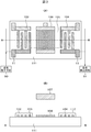
- FIG. 1 (A) is a top view
- FIG. 1 (B) is a cross-sectional view along dotted line AB in FIG. 1 (A).
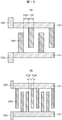
- the solid particle mass measuring apparatus includes a piezoelectric substrate 111 and an input electrode 103 and an output formed on the piezoelectric substrate 111 with a surface acoustic wave propagation region 105 as a propagation path of the surface acoustic wave 1 interposed therebetween.
- An electrode 104 is provided.
- the input electrode 103 is provided at one end of the piezoelectric substrate 111 to excite the surface acoustic wave 1.
- the output electrode 104 is provided at the other end of the piezoelectric substrate 111 and receives the surface acoustic wave 1 which is excited by the input electrode 103 and propagates in the surface acoustic wave propagation region 105 on the piezoelectric substrate 111.
- a solid particle adhesion region 109 to which solid particles are attached is provided.
- a signal generation circuit 90 is connected to the input electrode 103 via the GND electrode 11.
- a signal detection circuit 91 is connected to the output electrode 104 via the GND electrode 11.
- the signal detection circuit 91 functions as a solid particle adhesion amount detection unit that detects the adhesion amount of solid particles adhering to the solid particle adhesion region 109.
- Signal detection circuit 91 (solid particle adhesion amount detection unit) propagates surface acoustic wave 1 propagating in surface acoustic wave propagation region 105 by the interaction between surface acoustic wave 1 and solid particles attached to solid particle adhesion region 109.
- the amount of adhesion of solid fine particles is detected by detecting the change in the phase of the surface acoustic wave 1 caused by the change in speed with the output electrode 104.
- the piezoelectric substrate 111 is a substrate in which a material having piezoelectricity is shaped into a plate.
- the material having piezoelectricity is, for example, well known as quartz, and has a function of expanding and contracting when an electric field is applied.
- the input electrode 103 and the output electrode 104 be formed of comb-like electrodes disposed to face in the direction perpendicular to the propagation direction of the surface acoustic wave 1. As shown in FIG. 1B, the input electrode 103 and the output electrode 104 are covered with an insulating film 112.
- the comb-shaped electrode which comprises the input electrode 103 and the output electrode 104 is demonstrated.
- the comb electrodes 103 and 104 electrically connect a plurality of electrode fingers 100, a pair of bus bars 101 that electrically bundle the plurality of electrode fingers 100, and the bus bars 101. And a terminal 102.
- the surface acoustic wave 1 having the same frequency as the high frequency electrical signal is excited in a direction orthogonal to the electrode finger 100.
- the propagating surface acoustic wave 1 is converted into a high frequency electrical signal of the same frequency as the surface acoustic wave 1.
- the comb-shaped input electrode 103 excites the surface acoustic wave 1
- the comb-shaped output electrode 104 receives the surface acoustic wave 1.
- the excited surface acoustic wave 1 propagates in a surface acoustic wave propagation region 105 as a propagation path and reaches the output electrode 104.
- the surface acoustic wave 1 that has reached the output electrode 104 is converted again into a high frequency electrical signal by the output electrode 104, is output to the electrical terminal 102 of the output electrode 104 as a high frequency electrical signal, and is detected by the signal detection circuit 91.
- the shape of the comb-shaped electrode is not limited to this, and surface acoustic wave The characteristics of the device may be changed to be optimum for the measurement of the amount of solid particles.
- the electrode width 132 of the electrode finger 100 constituting the comb-shaped electrode and the space 133 between the adjacent electrode fingers 100 are designed at 1 ⁇ 4 of the wavelength of the surface acoustic wave 1.
- the electrode width 132 of the electrode finger 100 constituting the split electrode and the space 133 between the adjacent electrode fingers 100 are designed at 1/8 of the wavelength of the surface acoustic wave 1. This enables low-loss measurement.
- the surface acoustic wave 1 generated by the input signal applied to the electrode propagates to both sides of the electrode.
- the propagation direction of the surface acoustic wave 1 is restricted to one direction by using. As a result, the level of the output high frequency electrical signal can be increased, and the detection accuracy can be improved.
- the first metal electrode 106 is formed so that at least a part of the surface acoustic wave propagation region 105 is overlapped.
- the solid fine particle adhesion area 109 is the surface of the first metal electrode 106 inside the surface acoustic wave propagation area 105.
- a second metal electrode 107 is provided on the top of the first metal electrode 106 so as to face the first metal electrode 106. Solid particles are efficiently attached to the first metal electrode 106 by applying a voltage between the first metal electrode 106 and the second metal electrode 107.
- a dust collection method there are DC electric field, corona discharge, thermophoresis and the like.
- a second metal electrode 107 is provided opposite to the first metal electrode 106 and the top of the first metal electrode 106, and the first metal electrode 106 and the second metal electrode 106 are formed.
- a DC voltage is applied between the metal electrodes 107 to adhere the solid fine particles to the first metal electrode 106.
- the solid fine particle adhesion area 109 is the surface of the first metal electrode 106 inside the surface acoustic wave propagation area 105.
- the solid fine particles attached to the solid fine particle adhering area 109 on the piezoelectric substrate 111 have a property of being reflected at the end of the area to which the surface acoustic wave 1 and the solid fine particles adhere, and the phase largely shifts in this reflection.
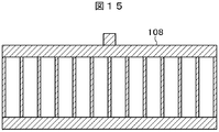
- an electrode formed of a plurality of grid-like electrodes is used as the first metal electrode 108 that functions as the solid fine particle adhesion region 109.
- the solid particles adhere to the surfaces of the plurality of grid electrodes.
- the area to which the solid fine particles attached to the solid fine particle adhering area 109 adhere is limited to a lattice, thereby increasing the phase shift amount due to the speed of sound and making the measurement sensitivity of the mass of solid fine particles.
- a grid-like first metal electrode 108 is provided in the surface acoustic wave propagation region 105, a voltage is applied to the metal electrode 107 in a gas containing solid fine particles, and an electric field is generated. Solid fine particles are attached to the grid-like first metal electrode 108.
- the configuration of the solid particulate matter mass measuring device according to the fourth embodiment will be described with reference to FIG.
- the area is covered with a plate-like mask 113.
- a gas introduction passage 201 for introducing a gas containing solid fine particles into the surface acoustic wave propagation region 105 is provided.
- the gas introduction path 201 is not limited to this structure, and the gas may be introduced by another structure.
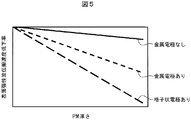
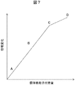
- FIG. 5 is a view showing the relationship between the surface acoustic wave propagation velocity reduction rate and the amount of adhesion of solid fine particles (PM) to the surface acoustic wave propagation path (PM thickness), from FIG. 11 (c) to FIG. It is an enlarged view of the AB part of (c).
- the reduction rate of the propagation speed is increased when the metal electrode is present, and the reduction rate of the propagation speed is further increased in the case of the grid electrode as compared with the case where the metal electrode is not provided.
- the propagation speed decrease rate corresponds to the change of the phase.
- both correspond to PM sensitivity it is understood that the sensitivity is improved by the metal electrode.
- the adhesion amount (mass) of solid fine particles can be estimated from the measurement of electric signal. It will be possible.
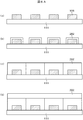
- FIG. 6A is a cross-sectional view taken along dotted line AB of the grid-like first metal electrode 108 shown in FIG. 3
- FIG. 6B is a top view of the grid-like first metal electrode 108 shown in FIG. It is.
- the solid fine particles 202 adhere to the lattice-like first metal electrode 108 in a lattice-like manner. Further, when solid particles are attached, as shown in FIG. 6A (c) and FIG. 6A (d), the solid particles are deposited and coat the grid-like first metal electrode 108.
- FIG. 7 shows the phase change of the surface acoustic wave when the solid fine particles adhere as shown in FIGS. 6A (a) to (d), and A to D in FIG. Each corresponds to d).
- the solid fine particles are deposited in a lattice, and as shown in FIGS. 6A (c) to 6 (d), the height is greater than the height of the latticed first metal electrode 108
- the sensitivity differs in the case where solid particles adhere to the The slopes of A to C in FIG. 7 are larger than the slopes of C to D in FIG. That is, it is understood that the detection sensitivity of the amount of solid fine particles is improved when the solid fine particles adhere in a lattice shape.
- the width 115 of the grid electrode and the spacing 114 of the adjacent grid electrodes are comb electrodes Make it smaller than the wavelength of the surface acoustic wave to be excited.
- the film thickness of the grid electrode is made sufficiently thick so that the sensitivity does not decrease even if the total mass of the attached solid fine particles is large.
- the shape of the grid electrode needs to be a shape that can be processed by a process.
- a grid electrode is formed with a ratio of electrode width to height, so-called aspect ratio, for example, 15: 1 or less.
- the surface acoustic wave 1 passing through the grid electrode interferes and strengthens by configuring the width 115 of the grid electrode and the interval 114 of the adjacent grid electrode to be 1/8 of the wavelength of the surface acoustic wave.
- the solid fine particles interact more strongly, and the detection sensitivity of the solid fine particles is improved.
- Example 1 a two-layer structure of platinum and titanium was used as a material of the input electrode 103, the output electrode 104, the first metal electrode 106, and the second metal electrode 107.
- the electrode material is not limited to platinum or titanium, and may be any material that transmits an electrical signal.
- the piezoelectric substrate 111 in which the temperature characteristics of the surface acoustic wave 1 do not change is used as the piezoelectric substrate 111, it is possible to perform measurement without being affected by environmental temperature changes with a mass measuring device, and realize a highly accurate measuring instrument. it can.
- the piezoelectric substrate 111 there are a quartz crystal, a langasite (La3Ga5SiO14) substrate, and the like, but another piezoelectric substrate having a good temperature stability may be used.
- an aluminum nitride thin film or an aluminum nitride thin film doped with Sc may be used.
- the piezoelectric substrate 111 is made of any of langasite, aluminum nitride thin film, or aluminum nitride thin film doped with Sc, sapphire, alumina, diamond, silicon carbide, and the electrode is made of platinum or titanium. If it is, it is possible to carry out the refresh operation (after the operation), so it is possible to realize a more accurate measuring instrument.
- the solid fine particles contain, for example, carbon as a main component.
- the solid particle measuring apparatus may be provided with means for heating the surface acoustic wave propagation area 105 and burning and removing solid particles attached to the solid particle adhering area 109.
- the surface acoustic wave device shown in FIG. 1 was prepared by the following process. After cleaning the surface of the piezoelectric substrate 111 and removing foreign substances on the surface, a pattern was formed by a photolithographic process, and a platinum pattern was formed by an electron beam vapor deposition apparatus, and then a comb electrode was formed by a lift-off process. .
- a titanium thin film was formed as an adhesive layer on the interface between the piezoelectric substrate 111 and platinum and on the platinum electrode.
- a silicon oxide film was formed to protect the comb electrode.
- removal of the silicon oxide film formed on the surface acoustic wave propagation region 105 of the surface acoustic wave 1 is not necessarily required.
- a voltage may be applied to the first metal electrodes 106 and 108 to collect the solid particles, causing a discharge and a charge accumulation in the silicon oxide film may occur to change the amount of adhesion of the solid particles. It is desirable to remove the silicon oxide film.
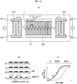
- FIG. 8 As a measuring element 121 that uses a pair of surface acoustic wave elements for measuring solid fine particles and attaches solid particles to one of the elements by means of solid particle collection means such as discharge. An element coated so that solid particles are not attached to one of the elements is used as a reference element 122, respectively.
- FIG. 9 is a cross-sectional view of the measurement element and the reference element of FIG. 8 taken along AA-BB and CC-DD, respectively.
- the window of the silicon oxide film 113 is opened in the solid particle adhesion area 109, and a gas introduction path 201 is provided.
- the solid fine particle adhering area 109 of the reference element 122 is completely covered with the silicon oxide film 113.
- the surface acoustic wave propagation region 105 of the reference side element (solid fine particles do not adhere) need not necessarily have the same electrode as the measuring element (the side to which solid fine particles adhere)
- the surface acoustic wave propagation region 105 of the measuring element 121 may be provided with a grid-like electrode 107, and the surface acoustic wave propagation region 105 of the reference element 122 may be provided with different electrodes.
- Example 2 since it is desirable that the measurement element 121 and the reference element 122 exhibit the same characteristic change depending on the environment due to changes in the measurement environment, in Example 2, the same grid-like electrode as the measurement element 121 and the reference element 122 Is used.
- the protective mask 113 is used to prevent interaction between the leak wave of the surface acoustic wave 1 and the deposit deposited on the coating film so that the solid particulates do not adhere to the reference element 122 and the solid particulates adhere only to the measuring element 121.
- the coating of the reference electrode was performed.
- the coating material of the reference element 122 may be any material, but it is desirable that the material be resistant to reaction, deformation or the like at an environmental temperature and an environmental atmosphere at which solid particles are measured.
- the element surface is coated with a silicon oxide film 112.
- the comb electrodes 103 and 104 may be used as a mask by covering with the coating plate 113 provided with a window on the solid particle adhesion region 109 so that solid particles are not attached.
- a solid film 110 (a flat film before patterning) is used as the solid particle adhesion region 109 to collect the solid particles (PM).
- a DC voltage 106 (DC bias) is applied to the solid film 110.
- the solid fine particles (PM) are attracted to the electric field, and are uniformly deposited on the solid film 110 as the solid fine particle adhesion region 109 and adhere.
- FIG. 11C it can be seen that the sensitivity is low in AC.
- the first metal electrode 108 functioning as the solid fine particle adhesion region 109 is formed of a plurality of grid-like electrodes. Use the electrode. The solid particles adhere to the periphery of the plurality of grid electrodes.
- the pitch of the grid of the grid electrode 108 is half or less of the wavelength.
- the solid fine particles (PM) are attracted to the electric field and are deposited while providing a level difference.
- This step has the effect of stopping the surface acoustic wave 1 (SAW).
- SAW surface acoustic wave 1
- FIGS. 13A and 13B show estimates of the reflection angle according to the principle of Hoiens.
- P is the pitch of the grid.
- Equation 1 waves incident on the grating are reflected in the direction of ⁇ .
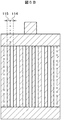
- the configuration of the solid particulate matter mass measurement device of the eighth embodiment will be described with reference to FIG.
- the grid electrode 108 is thinned as compared with the seventh embodiment (see FIG. 12).
- the solid fine particles (PM) are attracted to the electric field and are deposited while providing a level difference.
- FIG. 14C it can be seen that in Example 8, the sensitivity is higher than in Example 7 in the region A-C where the PM adhesion amount is low.
- the configuration of the solid particulate matter mass measurement device of the ninth embodiment will be described with reference to FIGS. 16 to 18.
- the grid electrode 108 is thinned and partially compared to the eighth embodiment (see FIG. 14). Is filled.
- the sensitivity can be made constant in the region of use. For example, when it is desired to use the areas A to E in FIG. 14B, the sensitivity is constant in the areas A to E as shown in FIG. Can be
- the sensitivity in the regions B to D as shown in FIG. 16C depending on the degree of thinning and filling of the grid electrode 108 can be fixed.
- a pattern shown in FIG. 16 a pattern shown in FIG. 17, or a pattern shown in FIG. 18 is appropriately selected and used as the degree of thinning and filling of the grid electrode 108.
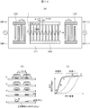
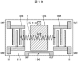
- FIG. 19 the configuration of the solid particulate matter mass measurement device of the tenth embodiment will be described with reference to FIGS. 19 and 20.
- FIG. 19 the solid fine particle adhesion area 109 is formed by the first metal electrode 106 provided in the surface acoustic wave propagation area 109.
- a heater and resistance thermometer 190 are disposed for the first metal electrode 106.
- the first metal electrode 106 functioning as the solid fine particle adhesion region 109 is heated to a high temperature (for example, 600 ° C. or higher) by the heater and resistance thermometer 190 and adhered to the first metal electrode 106 Remove solid particulates (PM).
- a high temperature for example, 600 ° C. or higher
- the heater and resistance thermometer 190 adhered to the first metal electrode 106 Remove solid particulates (PM).
- PM solid particulates
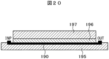
- the heater and the resistance thermometer 190 are integrally formed in FIG. 19, the heater and the resistance thermometer may be separately formed. Further, as shown in FIG. 20, the adhesive layer 196 and the SAW element 197 may be mounted on the ceramic substrate 195, and the heater and resistance thermometer 190 may be disposed between the ceramic substrate 195 and the adhesive layer 196.
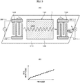
- the output (phase or delay time) of the sensor is measured (1) (S210), and the absolute value of the PM adhesion amount is determined (S211).
- the output of the sensor is measured (2) (S212).
- S213 From the measurement (2) result of the output of the sensor, it is determined whether or not it is in a saturated state (S213).
- the heater and resistance thermometer 190 are energized to reach a desired temperature (S214). After energizing the heater and resistance thermometer 190, refresh is performed (S215), and the energization is turned off (S216). If the saturated state is not obtained in S213, the PM adhesion amount per unit time is calculated from the difference between the output (1) and the output (2) (S217).
- the PM adhesion amount per unit time is output (OUT) (S218).
- the PM emission amount of the engine can be determined by multiplying the PM adhesion amount by a factor. Then, it is preferable to use the output difference from the reference element 122 of the fifth embodiment shown in FIG. 8 as the output of the sensor, because the influence of the temperature dependency can be eliminated.
- the eleventh embodiment is a modification of the solid particulate matter mass measurement device of the ninth embodiment shown in FIG.
- FIG. 22A is a top view
- FIG. 22B is a cross-sectional view of the vicinity of the center of the grid-like metal electrode 108.
- the insulating film 220 is formed on the metal 230.
- the piezoelectric substrate 111 does not have to be rectangular, and may be, for example, a parallelogram.
- the surface acoustic wave (SAW) 1 that has passed through the output electrode 104 is prevented from passing again through the output electrode 104, and the sensitivity is stabilized.
- FIG. 23B shows the sensitivity when the surface acoustic wave (SAW) 1 passes through the output electrode 104 again. As shown in FIG. 23B, it can be seen that the sensitivity in the case of repassing is not constant. In Example 12, the sensitivity in the case of repassing becomes constant.
- a reflector 240 is provided to double as an input / output electrode.
- the sensitivity is doubled.
- the switch 1 (241) and the switch 2 (242) are connected to the signal generation circuit 90 (S250).
- the signal generation circuit 90 outputs a signal (S251).
- the surface acoustic wave (SAW) 1 is excited by the input electrode (comb electrode) 103 (S 252).
- the surface acoustic wave (SAW) 1 passes through the solid fine particle adhesion area 109, is reflected by the reflector 240, and passes through the solid fine particle adhesion area 109 again (S253).
- the switch 1 (241) and the switch 2 (242) are connected to the signal detection circuit 91 (S254).
- the signal detection circuit 91 measures the delay time and the phase amount (S255).
- the PM emission amount is output (S256).
- Example 13 since the surface acoustic wave 1 passes through the solid fine particle adhesion region 109 twice, the sensitivity can be doubled.
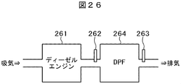
- Example 14 a DPF (Diesel Particulate Filter) is configured using the solid particle mass measuring device shown in FIG. 14 and the solid particle mass measuring device shown in FIG.
- the low sensitivity PM sensor 262 of FIG. 14 is disposed between the diesel engine 261 and the DPF 264, and the high sensitivity PM sensor 263 of FIG. 16 is disposed behind the DPF 264.
- the location where the amount of PM is large becomes low in sensitivity and saturation becomes difficult.
- a place where the amount of PM is small has high sensitivity and high sensitivity sensing becomes possible.
- the content (mass) of the solid particles contained in the atmosphere can be determined. It can be detected with high accuracy.
Landscapes
- Physics & Mathematics (AREA)
- Acoustics & Sound (AREA)
- Health & Medical Sciences (AREA)
- Life Sciences & Earth Sciences (AREA)
- Chemical & Material Sciences (AREA)
- Analytical Chemistry (AREA)
- Biochemistry (AREA)
- General Health & Medical Sciences (AREA)
- General Physics & Mathematics (AREA)
- Immunology (AREA)
- Pathology (AREA)
- Investigating Or Analyzing Materials By The Use Of Ultrasonic Waves (AREA)
- Surface Acoustic Wave Elements And Circuit Networks Thereof (AREA)
Abstract
La présente invention concerne un dispositif de mesure de masse de microparticules solides qui inclut : une zone d'adhérence (109) de microparticules solides qui est disposée au niveau d'une zone de propagation d'ondes élastiques de surface (105) et à laquelle on fait adhérer des microparticules solides ; et une unité de détection de quantité (circuit de détection de signaux) (91) d'adhérence de microparticules solides qui détecte la quantité d'adhérence de microparticules solides adhérant à la zone d'adhérence de microparticules solides.
Applications Claiming Priority (2)
| Application Number | Priority Date | Filing Date | Title |
|---|---|---|---|
| JP2017220689A JP2019090742A (ja) | 2017-11-16 | 2017-11-16 | 固体微粒子質量測定装置 |
| JP2017-220689 | 2017-11-16 |
Publications (1)
| Publication Number | Publication Date |
|---|---|
| WO2019097769A1 true WO2019097769A1 (fr) | 2019-05-23 |
Family
ID=66540177
Family Applications (1)
| Application Number | Title | Priority Date | Filing Date |
|---|---|---|---|
| PCT/JP2018/028452 WO2019097769A1 (fr) | 2017-11-16 | 2018-07-30 | Dispositif de mesure de masse de microparticules solides |
Country Status (2)
| Country | Link |
|---|---|
| JP (1) | JP2019090742A (fr) |
| WO (1) | WO2019097769A1 (fr) |
Cited By (2)
| Publication number | Priority date | Publication date | Assignee | Title |
|---|---|---|---|---|
| WO2020241867A1 (fr) * | 2019-05-31 | 2020-12-03 | 京セラ株式会社 | Dispositif capteur |
| EP4016088A1 (fr) * | 2020-12-21 | 2022-06-22 | Hamilton Sundstrand Corporation | Capteurs d'onde acoustique de surface pour sondes de données aériennes |
Citations (8)
| Publication number | Priority date | Publication date | Assignee | Title |
|---|---|---|---|---|
| GB2371362A (en) * | 2001-01-18 | 2002-07-24 | Univ Nottingham Trent | Monitoring apparatus and method for detecting particles in a gas stream using ionisation means and a SAW detector |
| JP2003502616A (ja) * | 1998-11-04 | 2003-01-21 | ローベルト ボツシユ ゲゼルシヤフト ミツト ベシユレンクテル ハフツング | 液体の濃度及び粘性を検出するセンサ装置及び方法 |
| JP2004069686A (ja) * | 2002-06-24 | 2004-03-04 | Particle Measuring Syst Inc | 分子汚染モニタリングシステムおよび分子汚染モニタリング方法 |
| JP2008275503A (ja) * | 2007-05-01 | 2008-11-13 | Japan Radio Co Ltd | 密度測定装置 |
| JP2009109261A (ja) * | 2007-10-29 | 2009-05-21 | Tama Tlo Kk | 弾性表面波ガス・センサ装置 |
| WO2013108608A1 (fr) * | 2012-01-20 | 2013-07-25 | パナソニック株式会社 | Capteur d'onde élastique |
| JP2015081861A (ja) * | 2013-10-23 | 2015-04-27 | ファインクリスタル株式会社 | 表面弾性波センサおよび表面弾性波センサ装置 |
| JP2015210080A (ja) * | 2014-04-23 | 2015-11-24 | 日本無線株式会社 | 弾性表面波センサ |
-
2017
- 2017-11-16 JP JP2017220689A patent/JP2019090742A/ja active Pending
-
2018
- 2018-07-30 WO PCT/JP2018/028452 patent/WO2019097769A1/fr active Application Filing
Patent Citations (8)
| Publication number | Priority date | Publication date | Assignee | Title |
|---|---|---|---|---|
| JP2003502616A (ja) * | 1998-11-04 | 2003-01-21 | ローベルト ボツシユ ゲゼルシヤフト ミツト ベシユレンクテル ハフツング | 液体の濃度及び粘性を検出するセンサ装置及び方法 |
| GB2371362A (en) * | 2001-01-18 | 2002-07-24 | Univ Nottingham Trent | Monitoring apparatus and method for detecting particles in a gas stream using ionisation means and a SAW detector |
| JP2004069686A (ja) * | 2002-06-24 | 2004-03-04 | Particle Measuring Syst Inc | 分子汚染モニタリングシステムおよび分子汚染モニタリング方法 |
| JP2008275503A (ja) * | 2007-05-01 | 2008-11-13 | Japan Radio Co Ltd | 密度測定装置 |
| JP2009109261A (ja) * | 2007-10-29 | 2009-05-21 | Tama Tlo Kk | 弾性表面波ガス・センサ装置 |
| WO2013108608A1 (fr) * | 2012-01-20 | 2013-07-25 | パナソニック株式会社 | Capteur d'onde élastique |
| JP2015081861A (ja) * | 2013-10-23 | 2015-04-27 | ファインクリスタル株式会社 | 表面弾性波センサおよび表面弾性波センサ装置 |
| JP2015210080A (ja) * | 2014-04-23 | 2015-11-24 | 日本無線株式会社 | 弾性表面波センサ |
Cited By (6)
| Publication number | Priority date | Publication date | Assignee | Title |
|---|---|---|---|---|
| WO2020241867A1 (fr) * | 2019-05-31 | 2020-12-03 | 京セラ株式会社 | Dispositif capteur |
| JPWO2020241867A1 (fr) * | 2019-05-31 | 2020-12-03 | ||
| CN113924483A (zh) * | 2019-05-31 | 2022-01-11 | 京瓷株式会社 | 传感器装置 |
| JP7231725B2 (ja) | 2019-05-31 | 2023-03-01 | 京セラ株式会社 | センサ装置 |
| EP4016088A1 (fr) * | 2020-12-21 | 2022-06-22 | Hamilton Sundstrand Corporation | Capteurs d'onde acoustique de surface pour sondes de données aériennes |
| US11549914B2 (en) | 2020-12-21 | 2023-01-10 | Hamilton Sundstrand Corporation | Surface acoustic wave sensors for air data probes |
Also Published As
| Publication number | Publication date |
|---|---|
| JP2019090742A (ja) | 2019-06-13 |
Similar Documents
| Publication | Publication Date | Title |
|---|---|---|
| US7285894B1 (en) | Surface acoustic wave devices for high temperature applications | |
| JP2013122439A (ja) | 粒子状物質センサーユニットおよびその製造方法 | |
| WO2019097769A1 (fr) | Dispositif de mesure de masse de microparticules solides | |
| KR100706561B1 (ko) | 마이크로 음향 센서 장치를 작동시키기 위한 방법 및 장치 | |
| CN110231095A (zh) | 一种等离激元声表面波谐振红外传感器 | |
| Giffney et al. | A surface acoustic wave ethanol sensor with zinc oxide nanorods | |
| JP6477120B2 (ja) | 物理量センサ | |
| JP2004093574A (ja) | 原子間力顕微鏡用力方位センサ付カンチレバー | |
| KR100698439B1 (ko) | 휘발성 물질 감지용 표면탄성파 가스센서 | |
| GB2371362A (en) | Monitoring apparatus and method for detecting particles in a gas stream using ionisation means and a SAW detector | |
| JP6558029B2 (ja) | 弾性表面波素子およびそれを用いた物理量センサ | |
| CA2549837A1 (fr) | Capteur, systeme de capteur et procede de mesure | |
| Priya et al. | A comparison of surface acoustic wave (SAW) delay line modelling techniques for sensor applications | |
| US20210265974A1 (en) | Film bulk acoustic sensors using thin ln-lt layer | |
| US7193352B1 (en) | Thin film bulk acoustic wave sensor suite | |
| JP6317567B2 (ja) | 粒子センサ | |
| JP2006337332A (ja) | 物質検出装置 | |
| JP2020088539A (ja) | 表面弾性波素子および固体微粒子質量測定装置 | |
| JP4003373B2 (ja) | 表面弾性波音速評価法 | |
| Kumar et al. | Design and simulation of polyisobutylene/silicon nitride for detection of gas sensing | |
| JP2008180668A (ja) | ラム波型高周波センサデバイス | |
| KR20160124384A (ko) | 입자농도측정용 센서소자 | |
| JP2005265423A (ja) | 表面弾性波デバイス | |
| Lim et al. | MEMS sensor for particulate matter measurement of exhaust gas | |
| JP3959532B2 (ja) | 超音波接触位置検出装置 |
Legal Events
| Date | Code | Title | Description |
|---|---|---|---|
| 121 | Ep: the epo has been informed by wipo that ep was designated in this application |
Ref document number: 18879696 Country of ref document: EP Kind code of ref document: A1 |
|
| NENP | Non-entry into the national phase |
Ref country code: DE |
|
| 122 | Ep: pct application non-entry in european phase |
Ref document number: 18879696 Country of ref document: EP Kind code of ref document: A1 |