WO2019097769A1 - Solid microparticle mass measurement device - Google Patents
Solid microparticle mass measurement device Download PDFInfo
- Publication number
- WO2019097769A1 WO2019097769A1 PCT/JP2018/028452 JP2018028452W WO2019097769A1 WO 2019097769 A1 WO2019097769 A1 WO 2019097769A1 JP 2018028452 W JP2018028452 W JP 2018028452W WO 2019097769 A1 WO2019097769 A1 WO 2019097769A1
- Authority
- WO
- WIPO (PCT)
- Prior art keywords
- solid
- electrode
- surface acoustic
- acoustic wave
- mass measuring
- Prior art date
Links
Images


Classifications
-
- G—PHYSICS
- G01—MEASURING; TESTING
- G01N—INVESTIGATING OR ANALYSING MATERIALS BY DETERMINING THEIR CHEMICAL OR PHYSICAL PROPERTIES
- G01N29/00—Investigating or analysing materials by the use of ultrasonic, sonic or infrasonic waves; Visualisation of the interior of objects by transmitting ultrasonic or sonic waves through the object
- G01N29/02—Analysing fluids
- G01N29/024—Analysing fluids by measuring propagation velocity or propagation time of acoustic waves
-
- H—ELECTRICITY
- H03—ELECTRONIC CIRCUITRY
- H03H—IMPEDANCE NETWORKS, e.g. RESONANT CIRCUITS; RESONATORS
- H03H9/00—Networks comprising electromechanical or electro-acoustic devices; Electromechanical resonators
- H03H9/02—Details
- H03H9/125—Driving means, e.g. electrodes, coils
- H03H9/145—Driving means, e.g. electrodes, coils for networks using surface acoustic waves
Definitions
- the present invention relates to a solid particle mass measuring device.
- Exhaust gas from an internal combustion engine such as a diesel engine includes solid particulates such as soot, so-called PM (Particle Matter), and air pollution by the solid particulates is a problem worldwide.
- PM Pularticle Matter
- Patent Documents 1 and 2 are mentioned, for example.
- a comb-shaped electrode is provided on a ceramic substrate, a bias is applied between the electrodes, and the resistance value of solid fine particles attached between the electrodes is measured to detect solid fine particles contained in exhaust gas. doing.
- An object of the present invention is to detect the content of solid fine particles contained in a gas with high sensitivity.
- the solid particle mass measuring device is a solid particle mass measuring device for measuring the content of solid particles contained in a gas, which is provided on a piezoelectric substrate and one end of the piezoelectric substrate, and has surface elasticity.
- An input electrode which excites a wave
- an output electrode which is provided at the other end of the piezoelectric substrate and receives the surface acoustic wave which is excited by the input electrode and propagates a surface acoustic wave propagation region on the piezoelectric substrate; Having a solid particle adhesion region provided in the surface acoustic wave propagation region and adhering the solid particles, and a solid particle adhesion amount detection unit detecting the adhesion amount of the solid particles adhered to the solid particle adhesion region It features.
- the content of solid fine particles contained in a gas can be detected with high sensitivity.
- FIG. 1 is a view showing the configuration of a solid particulate matter mass measuring device according to a first embodiment.
- FIG. 7 is a view showing another configuration of the solid particulate matter mass measurement device of Example 2.
- FIG. 18 is a view showing another configuration of the solid particulate matter mass measurement device of Example 3.
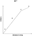
- FIG. 18 is a view showing another configuration of the solid particulate matter mass measurement device of Example 4. It is a figure which shows the relationship between the propagation velocity fall rate of surface acoustic wave, and the adhesion amount (PM thickness) to the surface acoustic wave propagation path of solid particulates (PM). It is a figure which shows the adhesion state of the solid fine particle to the grid
- FIG. 16 is a view showing the configuration of a solid particulate matter mass measurement device of Example 5.
- FIG. 16 is a view showing the configuration of a solid particulate matter mass measurement device of Example 5.
- FIG. 16 is a view showing the configuration of a solid particulate matter mass measurement device of Example 6.
- FIG. 16 is a diagram showing the configuration of a solid particulate matter mass measurement device according to a seventh example.
- FIG. 16 is a diagram showing the configuration of a solid particulate matter mass measurement device of Example 8.
- FIG. 16 is a view showing the configuration of a grid-like electrode of the solid fine particle mass measuring device of Example 8.
- FIG. 18 is a view showing the configuration of a solid particulate matter mass measurement device of Example 9.
- FIG. 16 is a view showing the configuration of a grid-like electrode of the solid fine particle mass measuring device of Example 9;
- FIG. 18 is a view showing another configuration of the grid-like electrode of the solid fine particle mass measuring device of Example 9.
- FIG. 18 is a view showing the configuration of a solid particulate matter mass measurement device of Example 10.
- FIG. 18 is a view showing another configuration of the solid particulate matter mass measurement device of Example 10.
- FIG. 18 is a view showing the operation of the solid fine particle mass measuring device of the tenth embodiment.
- FIG. 18 is a view showing the configuration of a solid particulate matter mass measurement device of Example 11.
- FIG. 18 is a diagram showing the configuration of a solid particulate matter mass measurement device of Example 12.
- FIG. 18 is a diagram showing the configuration of a solid particulate matter mass measurement device of Example 13.
- FIG. 18 is a view showing the operation of the solid fine particle mass measuring device of the thirteenth embodiment.
- FIG. 18 is a diagram showing the configuration of a solid particulate matter mass measurement device of Example 14.
- the embodiment of the present invention relates to a solid particle mass measuring device for solid particles using a surface acoustic wave device (SAW), which detects with high sensitivity the content (mass) of solid particles such as soot contained in exhaust gas.
- SAW surface acoustic wave device
- ionized solid fine particles are collected and attached on a propagation path using a surface acoustic wave device that causes surface acoustic waves to propagate by a pair of electrodes formed on a piezoelectric substrate.
- a surface acoustic wave device that causes surface acoustic waves to propagate by a pair of electrodes formed on a piezoelectric substrate.
- the content (mass) of the solid fine particles contained in the air is detected with high accuracy.
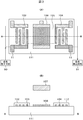
- FIG. 1 (A) is a top view
- FIG. 1 (B) is a cross-sectional view along dotted line AB in FIG. 1 (A).
- the solid particle mass measuring apparatus includes a piezoelectric substrate 111 and an input electrode 103 and an output formed on the piezoelectric substrate 111 with a surface acoustic wave propagation region 105 as a propagation path of the surface acoustic wave 1 interposed therebetween.
- An electrode 104 is provided.
- the input electrode 103 is provided at one end of the piezoelectric substrate 111 to excite the surface acoustic wave 1.
- the output electrode 104 is provided at the other end of the piezoelectric substrate 111 and receives the surface acoustic wave 1 which is excited by the input electrode 103 and propagates in the surface acoustic wave propagation region 105 on the piezoelectric substrate 111.
- a solid particle adhesion region 109 to which solid particles are attached is provided.
- a signal generation circuit 90 is connected to the input electrode 103 via the GND electrode 11.
- a signal detection circuit 91 is connected to the output electrode 104 via the GND electrode 11.
- the signal detection circuit 91 functions as a solid particle adhesion amount detection unit that detects the adhesion amount of solid particles adhering to the solid particle adhesion region 109.
- Signal detection circuit 91 (solid particle adhesion amount detection unit) propagates surface acoustic wave 1 propagating in surface acoustic wave propagation region 105 by the interaction between surface acoustic wave 1 and solid particles attached to solid particle adhesion region 109.
- the amount of adhesion of solid fine particles is detected by detecting the change in the phase of the surface acoustic wave 1 caused by the change in speed with the output electrode 104.
- the piezoelectric substrate 111 is a substrate in which a material having piezoelectricity is shaped into a plate.
- the material having piezoelectricity is, for example, well known as quartz, and has a function of expanding and contracting when an electric field is applied.
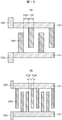
- the input electrode 103 and the output electrode 104 be formed of comb-like electrodes disposed to face in the direction perpendicular to the propagation direction of the surface acoustic wave 1. As shown in FIG. 1B, the input electrode 103 and the output electrode 104 are covered with an insulating film 112.
- the comb-shaped electrode which comprises the input electrode 103 and the output electrode 104 is demonstrated.
- the comb electrodes 103 and 104 electrically connect a plurality of electrode fingers 100, a pair of bus bars 101 that electrically bundle the plurality of electrode fingers 100, and the bus bars 101. And a terminal 102.
- the surface acoustic wave 1 having the same frequency as the high frequency electrical signal is excited in a direction orthogonal to the electrode finger 100.
- the propagating surface acoustic wave 1 is converted into a high frequency electrical signal of the same frequency as the surface acoustic wave 1.
- the comb-shaped input electrode 103 excites the surface acoustic wave 1
- the comb-shaped output electrode 104 receives the surface acoustic wave 1.
- the excited surface acoustic wave 1 propagates in a surface acoustic wave propagation region 105 as a propagation path and reaches the output electrode 104.
- the surface acoustic wave 1 that has reached the output electrode 104 is converted again into a high frequency electrical signal by the output electrode 104, is output to the electrical terminal 102 of the output electrode 104 as a high frequency electrical signal, and is detected by the signal detection circuit 91.
- the shape of the comb-shaped electrode is not limited to this, and surface acoustic wave The characteristics of the device may be changed to be optimum for the measurement of the amount of solid particles.
- the electrode width 132 of the electrode finger 100 constituting the comb-shaped electrode and the space 133 between the adjacent electrode fingers 100 are designed at 1 ⁇ 4 of the wavelength of the surface acoustic wave 1.
- the electrode width 132 of the electrode finger 100 constituting the split electrode and the space 133 between the adjacent electrode fingers 100 are designed at 1/8 of the wavelength of the surface acoustic wave 1. This enables low-loss measurement.
- the surface acoustic wave 1 generated by the input signal applied to the electrode propagates to both sides of the electrode.
- the propagation direction of the surface acoustic wave 1 is restricted to one direction by using. As a result, the level of the output high frequency electrical signal can be increased, and the detection accuracy can be improved.
- the first metal electrode 106 is formed so that at least a part of the surface acoustic wave propagation region 105 is overlapped.
- the solid fine particle adhesion area 109 is the surface of the first metal electrode 106 inside the surface acoustic wave propagation area 105.
- a second metal electrode 107 is provided on the top of the first metal electrode 106 so as to face the first metal electrode 106. Solid particles are efficiently attached to the first metal electrode 106 by applying a voltage between the first metal electrode 106 and the second metal electrode 107.
- a dust collection method there are DC electric field, corona discharge, thermophoresis and the like.
- a second metal electrode 107 is provided opposite to the first metal electrode 106 and the top of the first metal electrode 106, and the first metal electrode 106 and the second metal electrode 106 are formed.
- a DC voltage is applied between the metal electrodes 107 to adhere the solid fine particles to the first metal electrode 106.
- the solid fine particle adhesion area 109 is the surface of the first metal electrode 106 inside the surface acoustic wave propagation area 105.
- the solid fine particles attached to the solid fine particle adhering area 109 on the piezoelectric substrate 111 have a property of being reflected at the end of the area to which the surface acoustic wave 1 and the solid fine particles adhere, and the phase largely shifts in this reflection.
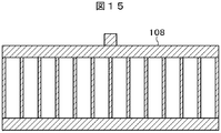
- an electrode formed of a plurality of grid-like electrodes is used as the first metal electrode 108 that functions as the solid fine particle adhesion region 109.
- the solid particles adhere to the surfaces of the plurality of grid electrodes.
- the area to which the solid fine particles attached to the solid fine particle adhering area 109 adhere is limited to a lattice, thereby increasing the phase shift amount due to the speed of sound and making the measurement sensitivity of the mass of solid fine particles.
- a grid-like first metal electrode 108 is provided in the surface acoustic wave propagation region 105, a voltage is applied to the metal electrode 107 in a gas containing solid fine particles, and an electric field is generated. Solid fine particles are attached to the grid-like first metal electrode 108.
- the configuration of the solid particulate matter mass measuring device according to the fourth embodiment will be described with reference to FIG.
- the area is covered with a plate-like mask 113.
- a gas introduction passage 201 for introducing a gas containing solid fine particles into the surface acoustic wave propagation region 105 is provided.
- the gas introduction path 201 is not limited to this structure, and the gas may be introduced by another structure.
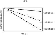
- FIG. 5 is a view showing the relationship between the surface acoustic wave propagation velocity reduction rate and the amount of adhesion of solid fine particles (PM) to the surface acoustic wave propagation path (PM thickness), from FIG. 11 (c) to FIG. It is an enlarged view of the AB part of (c).
- the reduction rate of the propagation speed is increased when the metal electrode is present, and the reduction rate of the propagation speed is further increased in the case of the grid electrode as compared with the case where the metal electrode is not provided.
- the propagation speed decrease rate corresponds to the change of the phase.
- both correspond to PM sensitivity it is understood that the sensitivity is improved by the metal electrode.
- the adhesion amount (mass) of solid fine particles can be estimated from the measurement of electric signal. It will be possible.
- FIG. 6A is a cross-sectional view taken along dotted line AB of the grid-like first metal electrode 108 shown in FIG. 3
- FIG. 6B is a top view of the grid-like first metal electrode 108 shown in FIG. It is.
- the solid fine particles 202 adhere to the lattice-like first metal electrode 108 in a lattice-like manner. Further, when solid particles are attached, as shown in FIG. 6A (c) and FIG. 6A (d), the solid particles are deposited and coat the grid-like first metal electrode 108.
- FIG. 7 shows the phase change of the surface acoustic wave when the solid fine particles adhere as shown in FIGS. 6A (a) to (d), and A to D in FIG. Each corresponds to d).
- the solid fine particles are deposited in a lattice, and as shown in FIGS. 6A (c) to 6 (d), the height is greater than the height of the latticed first metal electrode 108
- the sensitivity differs in the case where solid particles adhere to the The slopes of A to C in FIG. 7 are larger than the slopes of C to D in FIG. That is, it is understood that the detection sensitivity of the amount of solid fine particles is improved when the solid fine particles adhere in a lattice shape.
- the width 115 of the grid electrode and the spacing 114 of the adjacent grid electrodes are comb electrodes Make it smaller than the wavelength of the surface acoustic wave to be excited.
- the film thickness of the grid electrode is made sufficiently thick so that the sensitivity does not decrease even if the total mass of the attached solid fine particles is large.
- the shape of the grid electrode needs to be a shape that can be processed by a process.
- a grid electrode is formed with a ratio of electrode width to height, so-called aspect ratio, for example, 15: 1 or less.
- the surface acoustic wave 1 passing through the grid electrode interferes and strengthens by configuring the width 115 of the grid electrode and the interval 114 of the adjacent grid electrode to be 1/8 of the wavelength of the surface acoustic wave.
- the solid fine particles interact more strongly, and the detection sensitivity of the solid fine particles is improved.
- Example 1 a two-layer structure of platinum and titanium was used as a material of the input electrode 103, the output electrode 104, the first metal electrode 106, and the second metal electrode 107.
- the electrode material is not limited to platinum or titanium, and may be any material that transmits an electrical signal.
- the piezoelectric substrate 111 in which the temperature characteristics of the surface acoustic wave 1 do not change is used as the piezoelectric substrate 111, it is possible to perform measurement without being affected by environmental temperature changes with a mass measuring device, and realize a highly accurate measuring instrument. it can.
- the piezoelectric substrate 111 there are a quartz crystal, a langasite (La3Ga5SiO14) substrate, and the like, but another piezoelectric substrate having a good temperature stability may be used.
- an aluminum nitride thin film or an aluminum nitride thin film doped with Sc may be used.
- the piezoelectric substrate 111 is made of any of langasite, aluminum nitride thin film, or aluminum nitride thin film doped with Sc, sapphire, alumina, diamond, silicon carbide, and the electrode is made of platinum or titanium. If it is, it is possible to carry out the refresh operation (after the operation), so it is possible to realize a more accurate measuring instrument.
- the solid fine particles contain, for example, carbon as a main component.
- the solid particle measuring apparatus may be provided with means for heating the surface acoustic wave propagation area 105 and burning and removing solid particles attached to the solid particle adhering area 109.
- the surface acoustic wave device shown in FIG. 1 was prepared by the following process. After cleaning the surface of the piezoelectric substrate 111 and removing foreign substances on the surface, a pattern was formed by a photolithographic process, and a platinum pattern was formed by an electron beam vapor deposition apparatus, and then a comb electrode was formed by a lift-off process. .
- a titanium thin film was formed as an adhesive layer on the interface between the piezoelectric substrate 111 and platinum and on the platinum electrode.
- a silicon oxide film was formed to protect the comb electrode.
- removal of the silicon oxide film formed on the surface acoustic wave propagation region 105 of the surface acoustic wave 1 is not necessarily required.
- a voltage may be applied to the first metal electrodes 106 and 108 to collect the solid particles, causing a discharge and a charge accumulation in the silicon oxide film may occur to change the amount of adhesion of the solid particles. It is desirable to remove the silicon oxide film.
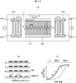
- FIG. 8 As a measuring element 121 that uses a pair of surface acoustic wave elements for measuring solid fine particles and attaches solid particles to one of the elements by means of solid particle collection means such as discharge. An element coated so that solid particles are not attached to one of the elements is used as a reference element 122, respectively.
- FIG. 9 is a cross-sectional view of the measurement element and the reference element of FIG. 8 taken along AA-BB and CC-DD, respectively.
- the window of the silicon oxide film 113 is opened in the solid particle adhesion area 109, and a gas introduction path 201 is provided.
- the solid fine particle adhering area 109 of the reference element 122 is completely covered with the silicon oxide film 113.
- the surface acoustic wave propagation region 105 of the reference side element (solid fine particles do not adhere) need not necessarily have the same electrode as the measuring element (the side to which solid fine particles adhere)
- the surface acoustic wave propagation region 105 of the measuring element 121 may be provided with a grid-like electrode 107, and the surface acoustic wave propagation region 105 of the reference element 122 may be provided with different electrodes.
- Example 2 since it is desirable that the measurement element 121 and the reference element 122 exhibit the same characteristic change depending on the environment due to changes in the measurement environment, in Example 2, the same grid-like electrode as the measurement element 121 and the reference element 122 Is used.
- the protective mask 113 is used to prevent interaction between the leak wave of the surface acoustic wave 1 and the deposit deposited on the coating film so that the solid particulates do not adhere to the reference element 122 and the solid particulates adhere only to the measuring element 121.
- the coating of the reference electrode was performed.
- the coating material of the reference element 122 may be any material, but it is desirable that the material be resistant to reaction, deformation or the like at an environmental temperature and an environmental atmosphere at which solid particles are measured.
- the element surface is coated with a silicon oxide film 112.
- the comb electrodes 103 and 104 may be used as a mask by covering with the coating plate 113 provided with a window on the solid particle adhesion region 109 so that solid particles are not attached.
- a solid film 110 (a flat film before patterning) is used as the solid particle adhesion region 109 to collect the solid particles (PM).
- a DC voltage 106 (DC bias) is applied to the solid film 110.
- the solid fine particles (PM) are attracted to the electric field, and are uniformly deposited on the solid film 110 as the solid fine particle adhesion region 109 and adhere.
- FIG. 11C it can be seen that the sensitivity is low in AC.
- the first metal electrode 108 functioning as the solid fine particle adhesion region 109 is formed of a plurality of grid-like electrodes. Use the electrode. The solid particles adhere to the periphery of the plurality of grid electrodes.
- the pitch of the grid of the grid electrode 108 is half or less of the wavelength.
- the solid fine particles (PM) are attracted to the electric field and are deposited while providing a level difference.
- This step has the effect of stopping the surface acoustic wave 1 (SAW).
- SAW surface acoustic wave 1
- FIGS. 13A and 13B show estimates of the reflection angle according to the principle of Hoiens.
- P is the pitch of the grid.
- Equation 1 waves incident on the grating are reflected in the direction of ⁇ .
- the configuration of the solid particulate matter mass measurement device of the eighth embodiment will be described with reference to FIG.
- the grid electrode 108 is thinned as compared with the seventh embodiment (see FIG. 12).
- the solid fine particles (PM) are attracted to the electric field and are deposited while providing a level difference.
- FIG. 14C it can be seen that in Example 8, the sensitivity is higher than in Example 7 in the region A-C where the PM adhesion amount is low.
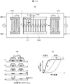
- the configuration of the solid particulate matter mass measurement device of the ninth embodiment will be described with reference to FIGS. 16 to 18.
- the grid electrode 108 is thinned and partially compared to the eighth embodiment (see FIG. 14). Is filled.
- the sensitivity can be made constant in the region of use. For example, when it is desired to use the areas A to E in FIG. 14B, the sensitivity is constant in the areas A to E as shown in FIG. Can be
- the sensitivity in the regions B to D as shown in FIG. 16C depending on the degree of thinning and filling of the grid electrode 108 can be fixed.
- a pattern shown in FIG. 16 a pattern shown in FIG. 17, or a pattern shown in FIG. 18 is appropriately selected and used as the degree of thinning and filling of the grid electrode 108.
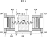
- FIG. 19 the configuration of the solid particulate matter mass measurement device of the tenth embodiment will be described with reference to FIGS. 19 and 20.
- FIG. 19 the solid fine particle adhesion area 109 is formed by the first metal electrode 106 provided in the surface acoustic wave propagation area 109.
- a heater and resistance thermometer 190 are disposed for the first metal electrode 106.
- the first metal electrode 106 functioning as the solid fine particle adhesion region 109 is heated to a high temperature (for example, 600 ° C. or higher) by the heater and resistance thermometer 190 and adhered to the first metal electrode 106 Remove solid particulates (PM).
- a high temperature for example, 600 ° C. or higher
- the heater and resistance thermometer 190 adhered to the first metal electrode 106 Remove solid particulates (PM).
- PM solid particulates
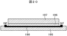
- the heater and the resistance thermometer 190 are integrally formed in FIG. 19, the heater and the resistance thermometer may be separately formed. Further, as shown in FIG. 20, the adhesive layer 196 and the SAW element 197 may be mounted on the ceramic substrate 195, and the heater and resistance thermometer 190 may be disposed between the ceramic substrate 195 and the adhesive layer 196.
- the output (phase or delay time) of the sensor is measured (1) (S210), and the absolute value of the PM adhesion amount is determined (S211).
- the output of the sensor is measured (2) (S212).
- S213 From the measurement (2) result of the output of the sensor, it is determined whether or not it is in a saturated state (S213).
- the heater and resistance thermometer 190 are energized to reach a desired temperature (S214). After energizing the heater and resistance thermometer 190, refresh is performed (S215), and the energization is turned off (S216). If the saturated state is not obtained in S213, the PM adhesion amount per unit time is calculated from the difference between the output (1) and the output (2) (S217).
- the PM adhesion amount per unit time is output (OUT) (S218).
- the PM emission amount of the engine can be determined by multiplying the PM adhesion amount by a factor. Then, it is preferable to use the output difference from the reference element 122 of the fifth embodiment shown in FIG. 8 as the output of the sensor, because the influence of the temperature dependency can be eliminated.
- the eleventh embodiment is a modification of the solid particulate matter mass measurement device of the ninth embodiment shown in FIG.
- FIG. 22A is a top view
- FIG. 22B is a cross-sectional view of the vicinity of the center of the grid-like metal electrode 108.
- the insulating film 220 is formed on the metal 230.
- the piezoelectric substrate 111 does not have to be rectangular, and may be, for example, a parallelogram.
- the surface acoustic wave (SAW) 1 that has passed through the output electrode 104 is prevented from passing again through the output electrode 104, and the sensitivity is stabilized.
- FIG. 23B shows the sensitivity when the surface acoustic wave (SAW) 1 passes through the output electrode 104 again. As shown in FIG. 23B, it can be seen that the sensitivity in the case of repassing is not constant. In Example 12, the sensitivity in the case of repassing becomes constant.
- a reflector 240 is provided to double as an input / output electrode.
- the sensitivity is doubled.
- the switch 1 (241) and the switch 2 (242) are connected to the signal generation circuit 90 (S250).
- the signal generation circuit 90 outputs a signal (S251).
- the surface acoustic wave (SAW) 1 is excited by the input electrode (comb electrode) 103 (S 252).
- the surface acoustic wave (SAW) 1 passes through the solid fine particle adhesion area 109, is reflected by the reflector 240, and passes through the solid fine particle adhesion area 109 again (S253).
- the switch 1 (241) and the switch 2 (242) are connected to the signal detection circuit 91 (S254).
- the signal detection circuit 91 measures the delay time and the phase amount (S255).
- the PM emission amount is output (S256).
- Example 13 since the surface acoustic wave 1 passes through the solid fine particle adhesion region 109 twice, the sensitivity can be doubled.
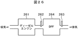
- Example 14 a DPF (Diesel Particulate Filter) is configured using the solid particle mass measuring device shown in FIG. 14 and the solid particle mass measuring device shown in FIG.
- the low sensitivity PM sensor 262 of FIG. 14 is disposed between the diesel engine 261 and the DPF 264, and the high sensitivity PM sensor 263 of FIG. 16 is disposed behind the DPF 264.
- the location where the amount of PM is large becomes low in sensitivity and saturation becomes difficult.
- a place where the amount of PM is small has high sensitivity and high sensitivity sensing becomes possible.
- the content (mass) of the solid particles contained in the atmosphere can be determined. It can be detected with high accuracy.
Abstract
This solid microparticle mass measurement device includes: a solid microparticle adherence region (109) which is disposed at a surface elastic wave propagation region (105) and to which solid microparticles are caused to adhere; and a solid microparticle adherence amount detection unit (signal detection circuit) (91) which detects the adherence amount of solid microparticles adhered to the solid microparticle adherence region.
Description
本発明は、固体微粒子質量測定装置に関する。
The present invention relates to a solid particle mass measuring device.
ディーゼルエンジンなどの内燃機関の排気ガスには、煤などの固体微粒子、いわゆるPM(Particle Matter)が含まれるが、この個体微粒子による大気汚染が世界的に問題となっている。
Exhaust gas from an internal combustion engine such as a diesel engine includes solid particulates such as soot, so-called PM (Particle Matter), and air pollution by the solid particulates is a problem worldwide.
排気ガスに含有し大気に排出される個体微粒子の量を制御するために、内燃機関の排気ガス管に微粒子センサを取り付け、個体微粒子の排出量を制御する試みがなされている。
In order to control the amount of solid particulates contained in exhaust gas and discharged to the atmosphere, attempts have been made to attach a particulate sensor to the exhaust gas pipe of an internal combustion engine to control the discharge amount of solid particulates.
このような微粒子センサに関連する技術として、例えば、特許文献1、2がる。特許文献1、2では、セラミック基板に櫛型の電極を設け、電極間にバイアスを印加し、電極間に付着した個体微粒子の抵抗値を測定することにより排気ガス中に含有する個体微粒子を検出している。
As a technique relevant to such a particulate sensor, patent documents 1 and 2 are mentioned, for example. In Patent Documents 1 and 2, a comb-shaped electrode is provided on a ceramic substrate, a bias is applied between the electrodes, and the resistance value of solid fine particles attached between the electrodes is measured to detect solid fine particles contained in exhaust gas. doing.
しかし、特許文献1、2に記載された微粒子センサにおいては、電極間に付着した個体微粒子により電極間が導通しないと個体微粒子の付着量を測定できない。このため、特許文献1、2では微量な個体微粒子を高感度に検出することは困難である。
本発明の目的は、気体中に含まれる固体微粒子の含有量を高感度に検出することにある。 However, in the particle sensor described in Patent Documents 1 and 2, the amount of adhesion of the solid particles can not be measured unless the electrodes are made conductive by the solid particles attached between the electrodes. For this reason, in patent documents 1 and 2, it is difficult to detect a minute amount of solid fine particles with high sensitivity.
An object of the present invention is to detect the content of solid fine particles contained in a gas with high sensitivity.
本発明の目的は、気体中に含まれる固体微粒子の含有量を高感度に検出することにある。 However, in the particle sensor described in
An object of the present invention is to detect the content of solid fine particles contained in a gas with high sensitivity.
本発明の一態様の固体微粒子質量測定装置は、気体中に含まれる固体微粒子の含有量を測定する固体微粒子質量測定装置であって、圧電基板と、前記圧電基板の一端に設けられ、表面弾性波を励起する入力電極と、前記圧電基板の他端に設けられ、前記入力電極で励起されて前記圧電基板上の表面弾性波伝搬領域を伝搬する前記表面弾性波を受信する出力電極と、前記表面弾性波伝搬領域に設けられ、前記固体微粒子を付着させる固体微粒子付着領域と、前記固体微粒子付着領域に付着した前記固体微粒子の付着量を検出する固体微粒子付着量検出部と、を有することを特徴とする。
The solid particle mass measuring device according to one aspect of the present invention is a solid particle mass measuring device for measuring the content of solid particles contained in a gas, which is provided on a piezoelectric substrate and one end of the piezoelectric substrate, and has surface elasticity. An input electrode which excites a wave, an output electrode which is provided at the other end of the piezoelectric substrate and receives the surface acoustic wave which is excited by the input electrode and propagates a surface acoustic wave propagation region on the piezoelectric substrate; Having a solid particle adhesion region provided in the surface acoustic wave propagation region and adhering the solid particles, and a solid particle adhesion amount detection unit detecting the adhesion amount of the solid particles adhered to the solid particle adhesion region It features.
本発明の一態様によれば、気体中に含まれる固体微粒子の含有量を高感度に検出することができる。
According to one aspect of the present invention, the content of solid fine particles contained in a gas can be detected with high sensitivity.
本発明の実施形態は、表面弾性波素子(SAW)を用いた固体微粒子の固体微粒子質量測定装置に関し、排ガス中に含まれる煤などの固体微粒子の含有量(質量)を高感度に検出する。具体的には、固体微粒子の含有量を見積もるために、圧電基板上に形成した一対の電極により表面弾性波を伝搬させる表面弾性波素子を用い、伝搬路上にイオン化した固体微粒子を収集し付着させる手段を設ける。これにより、大気中に含まれる固体微粒子の含有量(質量)を高精度に検出する。
以下、図面を用いて本発明の実施例について説明する。 The embodiment of the present invention relates to a solid particle mass measuring device for solid particles using a surface acoustic wave device (SAW), which detects with high sensitivity the content (mass) of solid particles such as soot contained in exhaust gas. Specifically, in order to estimate the content of solid fine particles, ionized solid fine particles are collected and attached on a propagation path using a surface acoustic wave device that causes surface acoustic waves to propagate by a pair of electrodes formed on a piezoelectric substrate. Provide a means. Thereby, the content (mass) of the solid fine particles contained in the air is detected with high accuracy.
Hereinafter, embodiments of the present invention will be described with reference to the drawings.
図1を参照して、実施例1の固体微粒子質量測定装置の構成について説明する。
ここで、図1(A)は上面図であり、図1(B)は図1(A)の点線A-Bに沿った断面図である。 The configuration of the solid particulate matter mass measuring device according to the first embodiment will be described with reference to FIG.
Here, FIG. 1 (A) is a top view, and FIG. 1 (B) is a cross-sectional view along dotted line AB in FIG. 1 (A).
図1に示すように、固体微粒子質量測定装置は、圧電基板111と、圧電基板111上に表面弾性波1の伝搬路である表面弾性波伝搬領域105を挟んで形成された入力電極103及び出力電極104を有する。
As shown in FIG. 1, the solid particle mass measuring apparatus includes a piezoelectric substrate 111 and an input electrode 103 and an output formed on the piezoelectric substrate 111 with a surface acoustic wave propagation region 105 as a propagation path of the surface acoustic wave 1 interposed therebetween. An electrode 104 is provided.
入力電極103は、圧電基板111の一端に設けられ表面弾性波1を励起する。出力電極104は、圧電基板111の他端に設けられ入力電極103で励起されて圧電基板111上の表面弾性波伝搬領域105を伝搬する表面弾性波1を受信する。
The input electrode 103 is provided at one end of the piezoelectric substrate 111 to excite the surface acoustic wave 1. The output electrode 104 is provided at the other end of the piezoelectric substrate 111 and receives the surface acoustic wave 1 which is excited by the input electrode 103 and propagates in the surface acoustic wave propagation region 105 on the piezoelectric substrate 111.
表面弾性波伝搬領域105の全部又は一部には、固体微粒子を付着させる固体微粒子付着領域109が設けられている。入力電極103には、信号発生回路90がGND電極11を介して接続されている。一方、出力電極104には、信号検出回路91がGND電極11を介して接続されている。信号検出回路91は、固体微粒子付着領域109に付着した固体微粒子の付着量を検出する固体微粒子付着量検出部として機能する。
In all or part of the surface acoustic wave propagation region 105, a solid particle adhesion region 109 to which solid particles are attached is provided. A signal generation circuit 90 is connected to the input electrode 103 via the GND electrode 11. On the other hand, a signal detection circuit 91 is connected to the output electrode 104 via the GND electrode 11. The signal detection circuit 91 functions as a solid particle adhesion amount detection unit that detects the adhesion amount of solid particles adhering to the solid particle adhesion region 109.
信号検出回路91(固体微粒子付着量検出部)は、固体微粒子付着領域109に付着した固体微粒子と表面弾性波1との相互作用により、表面弾性波1が表面弾性波伝搬領域105を伝搬する伝搬速度が変化することにより生じた表面弾性波1の位相の変化を出力電極104で検出することにより、固体微粒子の付着量を検出する。
Signal detection circuit 91 (solid particle adhesion amount detection unit) propagates surface acoustic wave 1 propagating in surface acoustic wave propagation region 105 by the interaction between surface acoustic wave 1 and solid particles attached to solid particle adhesion region 109. The amount of adhesion of solid fine particles is detected by detecting the change in the phase of the surface acoustic wave 1 caused by the change in speed with the output electrode 104.
圧電基板111は、圧電性を有する材料を板状に整形された基板である。圧電性を有する材料とは、例えば水晶などがよく知られており、電場を印加すると伸縮する機能を有する。
The piezoelectric substrate 111 is a substrate in which a material having piezoelectricity is shaped into a plate. The material having piezoelectricity is, for example, well known as quartz, and has a function of expanding and contracting when an electric field is applied.
入力電極103及び出力電極104は、表面弾性波1の伝搬方向に対して垂直方向に対向して配置された櫛型の電極により形成されるのが好ましい。図1(B)に示すように、入力電極103及び出力電極104は、絶縁膜112で被覆されている。
It is preferable that the input electrode 103 and the output electrode 104 be formed of comb-like electrodes disposed to face in the direction perpendicular to the propagation direction of the surface acoustic wave 1. As shown in FIG. 1B, the input electrode 103 and the output electrode 104 are covered with an insulating film 112.
図10を参照して、入力電極103及び出力電極104を構成する櫛型電極について説明する。
図10(A)に示すように、櫛型電極103、104は、複数の電極指100と、複数の電極指100を電気的に束ねる一対のバスバー101と、バスバー101により電気的に接続する電気端子102とで構成されている。電気端子102の間に高周波電気信号を印加すると、電極指100と直交する方向に高周波電気信号と同じ周波数の表面弾性波1を励振する。あるいは、伝搬してきた表面弾性波1を表面弾性波1と同じ周波数の高周波電気信号に変換する。このように、櫛型の入力電極103は表面弾性波1を励起し、櫛型の出力電極104は表面弾性波1を受信する。 With reference to FIG. 10, the comb-shaped electrode which comprises theinput electrode 103 and the output electrode 104 is demonstrated.
As shown in FIG. 10A, the comb electrodes 103 and 104 electrically connect a plurality of electrode fingers 100, a pair of bus bars 101 that electrically bundle the plurality of electrode fingers 100, and the bus bars 101. And a terminal 102. When a high frequency electrical signal is applied between the electrical terminals 102, the surface acoustic wave 1 having the same frequency as the high frequency electrical signal is excited in a direction orthogonal to the electrode finger 100. Alternatively, the propagating surface acoustic wave 1 is converted into a high frequency electrical signal of the same frequency as the surface acoustic wave 1. Thus, the comb-shaped input electrode 103 excites the surface acoustic wave 1, and the comb-shaped output electrode 104 receives the surface acoustic wave 1.
図10(A)に示すように、櫛型電極103、104は、複数の電極指100と、複数の電極指100を電気的に束ねる一対のバスバー101と、バスバー101により電気的に接続する電気端子102とで構成されている。電気端子102の間に高周波電気信号を印加すると、電極指100と直交する方向に高周波電気信号と同じ周波数の表面弾性波1を励振する。あるいは、伝搬してきた表面弾性波1を表面弾性波1と同じ周波数の高周波電気信号に変換する。このように、櫛型の入力電極103は表面弾性波1を励起し、櫛型の出力電極104は表面弾性波1を受信する。 With reference to FIG. 10, the comb-shaped electrode which comprises the
As shown in FIG. 10A, the
櫛型の入力電極103の電気端子102間に信号発生回路90により高周波電気信号を入力すると、圧電基板1上に電場が誘起されて電極指100に垂直な方向に表面弾性波1が励振される。
When a high frequency electric signal is input between the electric terminals 102 of the comb-shaped input electrode 103 by the signal generation circuit 90, an electric field is induced on the piezoelectric substrate 1 and the surface acoustic wave 1 is excited in the direction perpendicular to the electrode finger 100. .
励振された表面弾性波1は、伝搬路としての表面弾性波伝搬領域105を伝搬し出力電極104に到達する。出力電極104に到達した表面弾性波1は出力電極104で再び高周波電気信号に変換され、出力電極104の電気端子102に高周波電気信号として出力され信号検出回路91により検出される。
The excited surface acoustic wave 1 propagates in a surface acoustic wave propagation region 105 as a propagation path and reaches the output electrode 104. The surface acoustic wave 1 that has reached the output electrode 104 is converted again into a high frequency electrical signal by the output electrode 104, is output to the electrical terminal 102 of the output electrode 104 as a high frequency electrical signal, and is detected by the signal detection circuit 91.
表面弾性波伝搬領域105内に設けられた固体微粒子付着領域109に固体微粒子が付着すると、表面弾性波1と固体微粒子との相互作用により表面弾性波1の伝搬速度が変化し表面弾性波1の位相が変化する。この位相変化を出力電極104で出力される高周波電気信号の位相変化として検出することにより、固体微粒子の付着を検出することができる。
When solid particles adhere to the solid particle adhesion region 109 provided in the surface acoustic wave propagation region 105, the propagation velocity of the surface elastic wave 1 changes due to the interaction between the surface elastic wave 1 and the solid particles. The phase changes. By detecting this phase change as a phase change of the high frequency electric signal output from the output electrode 104, it is possible to detect the adhesion of solid fine particles.
なお、実施例1では、図1の入力電極103及び出力電極104として、図1及び図10に示す櫛型電極を用いたが、櫛形電極の形状はこれに限ったものではなく、表面弾性波素子の特性が固体微粒子量の測定に最適となるように変更してもよい。
Although the comb-shaped electrodes shown in FIGS. 1 and 10 are used as the input electrode 103 and the output electrode 104 in FIG. 1 in the first embodiment, the shape of the comb-shaped electrode is not limited to this, and surface acoustic wave The characteristics of the device may be changed to be optimum for the measurement of the amount of solid particles.
例えば、図10(A)に示すように、櫛型電極を構成する電極指100の電極幅132及び隣接する電極指100間のスペース133を表面弾性波1の波長の1/4で設計する。これにより、各電極で発生あるいは通過する表面弾性波同士が強め合うため低損失での測定が可能となる。
For example, as shown in FIG. 10A, the electrode width 132 of the electrode finger 100 constituting the comb-shaped electrode and the space 133 between the adjacent electrode fingers 100 are designed at 1⁄4 of the wavelength of the surface acoustic wave 1. As a result, surface acoustic waves generated or passed at each electrode strengthen each other, and measurement with low loss becomes possible.
また、図10(B)で示すスプリット電極を用いると、位相の歪が低減されるため、検出精度を向上することができる。また、スプリット電極を構成する電極指100の電極幅132及び隣接する電極指100間のスペース133を表面弾性波1の波長の1/8で設計する。これにより、低損失での測定が可能となる。
Further, when the split electrode shown in FIG. 10B is used, distortion in phase is reduced, so that detection accuracy can be improved. Further, the electrode width 132 of the electrode finger 100 constituting the split electrode and the space 133 between the adjacent electrode fingers 100 are designed at 1/8 of the wavelength of the surface acoustic wave 1. This enables low-loss measurement.
なお、図10(A)、図10(B)の櫛形電極は共に、電極に印加した入力信号により発生した表面弾性波1が電極の両側に伝搬してしまうが、例えば、一方向性電極を用いて表面弾性波1の伝搬方向を一方向に制限する。これにより、出力高周波電気信号のレベルを大きくすることができ、検出精度を向上することが可能となる。
In both of the comb-like electrodes shown in FIGS. 10A and 10B, the surface acoustic wave 1 generated by the input signal applied to the electrode propagates to both sides of the electrode. The propagation direction of the surface acoustic wave 1 is restricted to one direction by using. As a result, the level of the output high frequency electrical signal can be increased, and the detection accuracy can be improved.
図2を参照して、実施例2の固体微粒子質量測定装置の構成について説明する。
図2に示すように、表面弾性波伝搬領域105の少なくても一部が重なるように設けられた第1の金属電極106が形成される。固体微粒子付着領域109は、表面弾性波伝搬領域105の内側の第1の金属電極106の表面である。第1の金属電極106の上部には、第1の金属電極106と対向して第2の金属電極107が設けられている。第1の金属電極106と第2の金属電極107との間に電圧を印加することにより第1の金属電極106に固体微粒子を効率良く付着させる。 The configuration of the solid fine particle mass measuring device of the second embodiment will be described with reference to FIG.
As shown in FIG. 2, thefirst metal electrode 106 is formed so that at least a part of the surface acoustic wave propagation region 105 is overlapped. The solid fine particle adhesion area 109 is the surface of the first metal electrode 106 inside the surface acoustic wave propagation area 105. A second metal electrode 107 is provided on the top of the first metal electrode 106 so as to face the first metal electrode 106. Solid particles are efficiently attached to the first metal electrode 106 by applying a voltage between the first metal electrode 106 and the second metal electrode 107.
図2に示すように、表面弾性波伝搬領域105の少なくても一部が重なるように設けられた第1の金属電極106が形成される。固体微粒子付着領域109は、表面弾性波伝搬領域105の内側の第1の金属電極106の表面である。第1の金属電極106の上部には、第1の金属電極106と対向して第2の金属電極107が設けられている。第1の金属電極106と第2の金属電極107との間に電圧を印加することにより第1の金属電極106に固体微粒子を効率良く付着させる。 The configuration of the solid fine particle mass measuring device of the second embodiment will be described with reference to FIG.
As shown in FIG. 2, the
集塵方法としては、DC電界、コロナ放電、熱泳動などがある。図2では、表面弾性波伝搬領域109に、第1の金属電極106と第1の金属電極106の上部に対向して第2の金属電極107を設け、第1の金属電極106と第2の金属電極107の間にDC電圧を印加して第1の金属電極106に固体微粒子を付着させる。
As a dust collection method, there are DC electric field, corona discharge, thermophoresis and the like. In FIG. 2, in the surface acoustic wave propagation region 109, a second metal electrode 107 is provided opposite to the first metal electrode 106 and the top of the first metal electrode 106, and the first metal electrode 106 and the second metal electrode 106 are formed. A DC voltage is applied between the metal electrodes 107 to adhere the solid fine particles to the first metal electrode 106.
図3を参照して、実施例3の固体微粒子質量測定装置の構成について説明する。
図3では明示していないが、固体微粒子付着領域109は、表面弾性波伝搬領域105の内側の第1の金属電極106の表面である。圧電体基板111上の固体微粒子付着領域109に付着した固体微粒子は、表面弾性波1と固体微粒子が付着する領域の端部で反射する性質があり、この反射の際に位相が大きくシフトする。 The configuration of the solid particulate matter mass measurement device of the third embodiment will be described with reference to FIG.
Although not clearly shown in FIG. 3, the solid fineparticle adhesion area 109 is the surface of the first metal electrode 106 inside the surface acoustic wave propagation area 105. The solid fine particles attached to the solid fine particle adhering area 109 on the piezoelectric substrate 111 have a property of being reflected at the end of the area to which the surface acoustic wave 1 and the solid fine particles adhere, and the phase largely shifts in this reflection.
図3では明示していないが、固体微粒子付着領域109は、表面弾性波伝搬領域105の内側の第1の金属電極106の表面である。圧電体基板111上の固体微粒子付着領域109に付着した固体微粒子は、表面弾性波1と固体微粒子が付着する領域の端部で反射する性質があり、この反射の際に位相が大きくシフトする。 The configuration of the solid particulate matter mass measurement device of the third embodiment will be described with reference to FIG.
Although not clearly shown in FIG. 3, the solid fine
そこで、実施例3では、図3に示すように、固体微粒子付着領域109として機能する第1の金属電極108として、複数の格子状電極により形成された電極を用いる。固体微粒子は、複数の格子状電極の表面に付着する。
Therefore, in the third embodiment, as shown in FIG. 3, an electrode formed of a plurality of grid-like electrodes is used as the first metal electrode 108 that functions as the solid fine particle adhesion region 109. The solid particles adhere to the surfaces of the plurality of grid electrodes.
図3に示す構成では、固体微粒子付着領域109に付着した固体微粒子の付着する領域を格子状に制限することにより、音速による位相シフト量を増大し固体微粒子の質量の測定感度をさせる。
具体的には、図3に示すように、表面弾性波伝搬領域105に格子状の第1の金属電極108を設け、固体微粒子を含む気体中で金属電極107に電圧を印加し電界を起こし、格子状の第1の金属電極108に固体微粒子を付着させる。 In the configuration shown in FIG. 3, the area to which the solid fine particles attached to the solid fineparticle adhering area 109 adhere is limited to a lattice, thereby increasing the phase shift amount due to the speed of sound and making the measurement sensitivity of the mass of solid fine particles.
Specifically, as shown in FIG. 3, a grid-likefirst metal electrode 108 is provided in the surface acoustic wave propagation region 105, a voltage is applied to the metal electrode 107 in a gas containing solid fine particles, and an electric field is generated. Solid fine particles are attached to the grid-like first metal electrode 108.
具体的には、図3に示すように、表面弾性波伝搬領域105に格子状の第1の金属電極108を設け、固体微粒子を含む気体中で金属電極107に電圧を印加し電界を起こし、格子状の第1の金属電極108に固体微粒子を付着させる。 In the configuration shown in FIG. 3, the area to which the solid fine particles attached to the solid fine
Specifically, as shown in FIG. 3, a grid-like
図4を参照して、実施例4の固体微粒子質量測定装置の構成について説明する。
図4に示すように、固体微粒子の浮遊する領域を第2の金属電極107又は格子状電極を構成する第1の金属電極108の近傍に制限するため、板状のマスク113で覆う。 The configuration of the solid particulate matter mass measuring device according to the fourth embodiment will be described with reference to FIG.
As shown in FIG. 4, in order to limit the floating area of the solid fine particles to the vicinity of thesecond metal electrode 107 or the first metal electrode 108 constituting the grid electrode, the area is covered with a plate-like mask 113.
図4に示すように、固体微粒子の浮遊する領域を第2の金属電極107又は格子状電極を構成する第1の金属電極108の近傍に制限するため、板状のマスク113で覆う。 The configuration of the solid particulate matter mass measuring device according to the fourth embodiment will be described with reference to FIG.
As shown in FIG. 4, in order to limit the floating area of the solid fine particles to the vicinity of the
尚、図4(B)に示すように、表面弾性波伝搬領域105へ固体微粒子を含む気体を導入するガス導入路201を設けられている。尚、ガス導入路201は本構成に限ったものではなく、その他の構成によってガスを導入してもよい。
As shown in FIG. 4B, a gas introduction passage 201 for introducing a gas containing solid fine particles into the surface acoustic wave propagation region 105 is provided. In addition, the gas introduction path 201 is not limited to this structure, and the gas may be introduced by another structure.
図5は、表面弾性波の伝搬速度低下率と固体微粒子(PM)の表面弾性波伝搬路への付着量(PM厚さ)との関係を示す図であり、図11(c)から図13(c)のA-B部の拡大図である。
図5に示すように、金属電極がない場合に比べて、金属電極がある場合は伝搬速度の低下率が増加し、格子状電極の場合はさらに伝搬速度低下率が増加することが分かる。ここで、伝搬速度低下率は位相の変化に対応する。また、両者はPM感度に対応することから、金属電極により感度が向上することが分かる。 FIG. 5 is a view showing the relationship between the surface acoustic wave propagation velocity reduction rate and the amount of adhesion of solid fine particles (PM) to the surface acoustic wave propagation path (PM thickness), from FIG. 11 (c) to FIG. It is an enlarged view of the AB part of (c).
As shown in FIG. 5, it can be seen that the reduction rate of the propagation speed is increased when the metal electrode is present, and the reduction rate of the propagation speed is further increased in the case of the grid electrode as compared with the case where the metal electrode is not provided. Here, the propagation speed decrease rate corresponds to the change of the phase. Moreover, since both correspond to PM sensitivity, it is understood that the sensitivity is improved by the metal electrode.
なお、図5に示すように、高周波電気信号の位相変化に対応する固体微粒子の付着質量をあらかじめ測定し検量線を作成すると、電気信号の測定から固体微粒子の付着量(質量)を見積もることが可能になる。
In addition, as shown in FIG. 5, when the adhesion mass of solid fine particles corresponding to the phase change of the high frequency electric signal is measured in advance and a calibration curve is prepared, the adhesion amount (mass) of solid fine particles can be estimated from the measurement of electric signal. It will be possible.
なお、格子状電極の高さ以上に固体微粒子が付着した場合には、図5に示すように感度が変化する。ここで、図6Aは、図3に示す格子状の第1の金属電極108の点線A~Bにおける断面図であり、図6Bは図3に示す格子状の第1の金属電極108の上面図である。
When the solid fine particles adhere to the grid-like electrode or more, the sensitivity changes as shown in FIG. Here, FIG. 6A is a cross-sectional view taken along dotted line AB of the grid-like first metal electrode 108 shown in FIG. 3, and FIG. 6B is a top view of the grid-like first metal electrode 108 shown in FIG. It is.
図6A(b)に示すように、格子状の第1の金属電極108に格子状に固体微粒子202が付着する。さらに、固体微粒子を付着すると、図6A(c)、図6A(d)のように、固体微粒子が堆積し格子状の第1の金属電極108を被服する。
As shown in FIG. 6A (b), the solid fine particles 202 adhere to the lattice-like first metal electrode 108 in a lattice-like manner. Further, when solid particles are attached, as shown in FIG. 6A (c) and FIG. 6A (d), the solid particles are deposited and coat the grid-like first metal electrode 108.
図7は図6A(a)~(d)のように固体微粒子が付着した際の表面弾性波の位相変化を示したものであり、図7中のA~Dは図6A(a)~(d)にそれぞれ対応している。図6A(a)~(b)のように、固体微粒子が格子状に堆積した場合と図6A(c)~図6(d)のように格子状の第1の金属電極108の高さ以上に固体粒子が付着した場合とで感度が異なる。図7のA~Cの傾きのほうが、図7のC~Dの傾きより大きい。すなわち、格子状に固体微粒子が付着すると、固体微粒子量の検出感度が向上することが分かる。
FIG. 7 shows the phase change of the surface acoustic wave when the solid fine particles adhere as shown in FIGS. 6A (a) to (d), and A to D in FIG. Each corresponds to d). As shown in FIGS. 6A (a) to (b), the solid fine particles are deposited in a lattice, and as shown in FIGS. 6A (c) to 6 (d), the height is greater than the height of the latticed first metal electrode 108 The sensitivity differs in the case where solid particles adhere to the The slopes of A to C in FIG. 7 are larger than the slopes of C to D in FIG. That is, it is understood that the detection sensitivity of the amount of solid fine particles is improved when the solid fine particles adhere in a lattice shape.
図3に示す格子状の第1の金属電極108の構成では、検出感度を向上させるために、図6Bに示すように、格子電極の幅115と隣接する格子電極の間隔114を櫛型電極で励振される表面弾性波の波長より小さくする。
In the configuration of the grid-like first metal electrode 108 shown in FIG. 3, in order to improve detection sensitivity, as shown in FIG. 6B, the width 115 of the grid electrode and the spacing 114 of the adjacent grid electrodes are comb electrodes Make it smaller than the wavelength of the surface acoustic wave to be excited.
また、付着した固体微粒子の総質量が多くても感度が低下しないように、格子状電極の膜厚を十分厚くする。なお、格子電極のアスペクト比が大きくなりすぎると、格子電極が倒れたり形状の欠陥が生じやすくなったりする。このため、格子電極の形状はプロセスで加工可能な形状であることが必要である。実施例1では、電極幅と高さの比、いわゆるアスペクト比を、たとえば15:1以下で格子電極を作成する。
Also, the film thickness of the grid electrode is made sufficiently thick so that the sensitivity does not decrease even if the total mass of the attached solid fine particles is large. In addition, when the aspect ratio of the grid electrode becomes too large, the grid electrode may fall down or a shape defect may easily occur. Therefore, the shape of the grid electrode needs to be a shape that can be processed by a process. In the first embodiment, a grid electrode is formed with a ratio of electrode width to height, so-called aspect ratio, for example, 15: 1 or less.
なお、格子電極の幅115と隣接する格子電極の間隔114を表面弾性波の波長の1/8で構成することにより、格子電極を通過する表面弾性波1が干渉し強め合おう。この結果、固体微粒子がより強く相互作用し固体微粒子の検出感度が向上する。
The surface acoustic wave 1 passing through the grid electrode interferes and strengthens by configuring the width 115 of the grid electrode and the interval 114 of the adjacent grid electrode to be 1/8 of the wavelength of the surface acoustic wave. As a result, the solid fine particles interact more strongly, and the detection sensitivity of the solid fine particles is improved.
なお、実施例1では、入力電極103、出力電極104、第1の金属電極106、第2の金属電極107の電極の材料として白金とチタンとの2層構造を用いた。電極材料は白金やチタンに限ったものでなく、電気信号を通す材料であれば良い。
In Example 1, a two-layer structure of platinum and titanium was used as a material of the input electrode 103, the output electrode 104, the first metal electrode 106, and the second metal electrode 107. The electrode material is not limited to platinum or titanium, and may be any material that transmits an electrical signal.
しかし、白金のように高温でも酸化せず、形成した電極と圧電基板111との密着性及び電極の形状が容易に変化しない材料を用いると、高温で動作させることができる。また、高温下で固体微粒子を燃焼させることで、図7のD状態からA状態に戻すことが出来るため(リフレッシュ可能になるため)高感度を維持でき、高精度な測定器を実現できる。
However, when a material such as platinum is not oxidized even at high temperature, and the adhesion between the formed electrode and the piezoelectric substrate 111 and the shape of the electrode are not easily changed, operation can be performed at high temperature. Further, by burning the solid fine particles under high temperature, the D state shown in FIG. 7 can be returned to the A state (because it becomes refreshable), high sensitivity can be maintained, and a high accuracy measuring instrument can be realized.
また、圧電体基板111として、表面弾性波1の温度特性が変化しない圧電体基板を用いれば、質量測定装置で環境温度変化に対して影響を受けない測定が可能となり高精度な測定器を実現できる。圧電体基板111としては、水晶、ランガサイト(La3Ga5SiO14)基板などがあるが、温度安定性の良い他の圧電基板を使用しても良い。またアルミニウムナイトライド薄膜、またはScをドープしたアルミニウムナイトライド薄膜を使用しても良い。これら圧電薄膜を用いる場合、珪素、サファイヤ、アルミナ、ダイヤモンド、炭素化珪素を主原料とする基板上に成膜するとよい。
In addition, if a piezoelectric substrate in which the temperature characteristics of the surface acoustic wave 1 do not change is used as the piezoelectric substrate 111, it is possible to perform measurement without being affected by environmental temperature changes with a mass measuring device, and realize a highly accurate measuring instrument. it can. As the piezoelectric substrate 111, there are a quartz crystal, a langasite (La3Ga5SiO14) substrate, and the like, but another piezoelectric substrate having a good temperature stability may be used. Alternatively, an aluminum nitride thin film or an aluminum nitride thin film doped with Sc may be used. When using these piezoelectric thin films, it is preferable to form a film on a substrate whose main raw material is silicon, sapphire, alumina, diamond, or silicon carbide.
圧電基板111が、ランガサイト、アルミニウムナイトライド薄膜、またはScをドープしたアルミニウムナイトライド薄膜、サファイヤ、アルミナ、ダイヤモンド、炭素化珪素のいずれかで構成され、かつ、電極が白金やチタンで構成されている場合、(後術)リフレッシュ動作をさせることができるため、いっそう高精度な測定器を実現できる。
The piezoelectric substrate 111 is made of any of langasite, aluminum nitride thin film, or aluminum nitride thin film doped with Sc, sapphire, alumina, diamond, silicon carbide, and the electrode is made of platinum or titanium. If it is, it is possible to carry out the refresh operation (after the operation), so it is possible to realize a more accurate measuring instrument.
尚、固体微粒子は、例えば、炭素を主成分とする。固体微粒子測定装置において、表面弾性波伝搬領域105を加熱し固体微粒子付着領域109に付着した固体微粒子を燃焼除去する手段を設けても良い。
The solid fine particles contain, for example, carbon as a main component. The solid particle measuring apparatus may be provided with means for heating the surface acoustic wave propagation area 105 and burning and removing solid particles attached to the solid particle adhering area 109.
図1に示す表面弾性波素子は、以下のプロセス処理により作成した。
圧電体基板111の表面を洗浄し、表面の異物等を除去した後、ホトリソグラフィプロセスによりパターンを形成し、電子ビーム蒸着装置により白金パターンを成膜した後、リフトオフプロセスにより櫛型電極を形成した。 The surface acoustic wave device shown in FIG. 1 was prepared by the following process.
After cleaning the surface of thepiezoelectric substrate 111 and removing foreign substances on the surface, a pattern was formed by a photolithographic process, and a platinum pattern was formed by an electron beam vapor deposition apparatus, and then a comb electrode was formed by a lift-off process. .
圧電体基板111の表面を洗浄し、表面の異物等を除去した後、ホトリソグラフィプロセスによりパターンを形成し、電子ビーム蒸着装置により白金パターンを成膜した後、リフトオフプロセスにより櫛型電極を形成した。 The surface acoustic wave device shown in FIG. 1 was prepared by the following process.
After cleaning the surface of the
次に、圧電体基板111と白金の界面、および、白金電極上には接着層としてチタンの薄膜を形成した。実施例1では、櫛型電極の保護のため、酸化珪素膜を形成した。
なお、固体微粒子の測定に問題がなければ、表面弾性波1の表面弾性波伝搬領域105上に形成された酸化珪素膜の除去は必ずしも必要ではない。しかし、固体微粒子を収集するために第1の金属電極106、108への電圧印加により放電を起こし固体、酸化珪素膜中への電荷蓄積が起こり固体微粒子の付着量が変化する可能性があるため、酸化珪素膜は除去することが望ましい。 Next, a titanium thin film was formed as an adhesive layer on the interface between thepiezoelectric substrate 111 and platinum and on the platinum electrode. In Example 1, a silicon oxide film was formed to protect the comb electrode.
In addition, if there is no problem in the measurement of solid fine particles, removal of the silicon oxide film formed on the surface acousticwave propagation region 105 of the surface acoustic wave 1 is not necessarily required. However, a voltage may be applied to the first metal electrodes 106 and 108 to collect the solid particles, causing a discharge and a charge accumulation in the silicon oxide film may occur to change the amount of adhesion of the solid particles. It is desirable to remove the silicon oxide film.
なお、固体微粒子の測定に問題がなければ、表面弾性波1の表面弾性波伝搬領域105上に形成された酸化珪素膜の除去は必ずしも必要ではない。しかし、固体微粒子を収集するために第1の金属電極106、108への電圧印加により放電を起こし固体、酸化珪素膜中への電荷蓄積が起こり固体微粒子の付着量が変化する可能性があるため、酸化珪素膜は除去することが望ましい。 Next, a titanium thin film was formed as an adhesive layer on the interface between the
In addition, if there is no problem in the measurement of solid fine particles, removal of the silicon oxide film formed on the surface acoustic
図8、図9を参照して、実施例5の固体微粒子質量測定装置の構成について説明する。
実施例5では、図8のように、固体微粒子を測定するための表面弾性波素子を1対用い、片方の素子に放電等の固体粒子収集手段により固体粒子を付着し検出する測定素子121として、片方の素子には固体粒子を付着しないように被覆した素子を参照素子122としてそれぞれ用いる。 The configuration of the solid particulate matter mass measurement device of the fifth embodiment will be described with reference to FIGS. 8 and 9.
In the fifth embodiment, as shown in FIG. 8, as a measuringelement 121 that uses a pair of surface acoustic wave elements for measuring solid fine particles and attaches solid particles to one of the elements by means of solid particle collection means such as discharge. An element coated so that solid particles are not attached to one of the elements is used as a reference element 122, respectively.
実施例5では、図8のように、固体微粒子を測定するための表面弾性波素子を1対用い、片方の素子に放電等の固体粒子収集手段により固体粒子を付着し検出する測定素子121として、片方の素子には固体粒子を付着しないように被覆した素子を参照素子122としてそれぞれ用いる。 The configuration of the solid particulate matter mass measurement device of the fifth embodiment will be described with reference to FIGS. 8 and 9.
In the fifth embodiment, as shown in FIG. 8, as a measuring
図9は、図8の測定用素子と参照素子の、それぞれAA-BB、CC-DDにおける断面図である。
図9に示すように、測定用素子121には固体微粒子付着領域109に酸化珪素膜113の窓を開口しており、ガスの導入路201を設けている。一方、参照素子122の固体微粒子付着領域109は酸化珪素膜113で完全に覆っている。 FIG. 9 is a cross-sectional view of the measurement element and the reference element of FIG. 8 taken along AA-BB and CC-DD, respectively.
As shown in FIG. 9, in the measuringelement 121, the window of the silicon oxide film 113 is opened in the solid particle adhesion area 109, and a gas introduction path 201 is provided. On the other hand, the solid fine particle adhering area 109 of the reference element 122 is completely covered with the silicon oxide film 113.
図9に示すように、測定用素子121には固体微粒子付着領域109に酸化珪素膜113の窓を開口しており、ガスの導入路201を設けている。一方、参照素子122の固体微粒子付着領域109は酸化珪素膜113で完全に覆っている。 FIG. 9 is a cross-sectional view of the measurement element and the reference element of FIG. 8 taken along AA-BB and CC-DD, respectively.
As shown in FIG. 9, in the measuring
また、実施例2のように、同じ素子を一対として用い、たとえば両者の出力信号の差分を用いるなどして固体微粒子を測定することにより、測定における環境の変化による表面弾性波素子の特性変化を補償し正確な測定を行うことができる。なお、対として用いる素子のうち、参照側素子(固体微粒子が付着しない)の表面弾性波伝搬領域105には、必ずしも測定素子(固体微粒子が付着する側)と同じ電極を設ける必要はなく、例えば、測定素子121の表面弾性波伝搬領域105には格子状電極107を、参照素子122の表面弾性波伝搬領域105には金属電極106を設けるなど、両者で異なる電極を設けても良い。
Also, as in Example 2, using the same element as a pair, for example, by measuring the solid fine particles using the difference between the output signals of both, etc., the characteristic change of the surface acoustic wave element due to the change of the environment in the measurement Compensate and make accurate measurements. Among the elements used as a pair, the surface acoustic wave propagation region 105 of the reference side element (solid fine particles do not adhere) need not necessarily have the same electrode as the measuring element (the side to which solid fine particles adhere) The surface acoustic wave propagation region 105 of the measuring element 121 may be provided with a grid-like electrode 107, and the surface acoustic wave propagation region 105 of the reference element 122 may be provided with different electrodes.
ただし、測定環境の変化により測定素子121と参照素子122が環境により同じ特性変化を示すような電極構成をとることが望ましいため、実施例2では測定素子121と参照素子122とに同じ格子状電極を用いている。
However, since it is desirable that the measurement element 121 and the reference element 122 exhibit the same characteristic change depending on the environment due to changes in the measurement environment, in Example 2, the same grid-like electrode as the measurement element 121 and the reference element 122 Is used.
参照素子122に固体微粒子が付着せず、測定素子121のみに固体微粒子が付着するように、表面弾性波1の漏れ波と被服膜上に付着した堆積物が相互作用しないよう、保護マスク113で参照側電極の被服を行った。
The protective mask 113 is used to prevent interaction between the leak wave of the surface acoustic wave 1 and the deposit deposited on the coating film so that the solid particulates do not adhere to the reference element 122 and the solid particulates adhere only to the measuring element 121. The coating of the reference electrode was performed.
参照用素子122の被服材料は何でも良いが、固体微粒子を測定する環境温度及び環境雰囲気において反応、変形等をしにくい材料であることが望ましい。実施例2では、酸化珪素膜112で素子表面を被服する。また、櫛形電極103、104については、固体微粒子が付着しないように、固体微粒子付着領域109上に窓を設けた被服板113で覆いマスクとして用いても良い。
The coating material of the reference element 122 may be any material, but it is desirable that the material be resistant to reaction, deformation or the like at an environmental temperature and an environmental atmosphere at which solid particles are measured. In the second embodiment, the element surface is coated with a silicon oxide film 112. Further, the comb electrodes 103 and 104 may be used as a mask by covering with the coating plate 113 provided with a window on the solid particle adhesion region 109 so that solid particles are not attached.
図11を参照して、実施例6の固体微粒子質量測定装置の構成について説明する。
図11(A)に示すように、実施例6の固体微粒子質量測定装置では、固体微粒子付着領域109として、ベタ膜110(パターニングする前の平坦な膜)を用い、固体微粒子(PM)の集塵方法としては、ベタ膜110にDC電圧106(DC bias)を印加する。 The configuration of the solid particulate matter mass measurement device of the sixth embodiment will be described with reference to FIG.
As shown in FIG. 11A, in the solid particle mass measuring device of the sixth embodiment, a solid film 110 (a flat film before patterning) is used as the solidparticle adhesion region 109 to collect the solid particles (PM). As a dust method, a DC voltage 106 (DC bias) is applied to the solid film 110.
図11(A)に示すように、実施例6の固体微粒子質量測定装置では、固体微粒子付着領域109として、ベタ膜110(パターニングする前の平坦な膜)を用い、固体微粒子(PM)の集塵方法としては、ベタ膜110にDC電圧106(DC bias)を印加する。 The configuration of the solid particulate matter mass measurement device of the sixth embodiment will be described with reference to FIG.
As shown in FIG. 11A, in the solid particle mass measuring device of the sixth embodiment, a solid film 110 (a flat film before patterning) is used as the solid
このような構成では、図11(B)に示すように、固体微粒子(PM)は電界にひきつけられて、固体微粒子付着領域109としてのベタ膜110上に一様に堆積して付着する。図11(C)に示すように、A-Cでは感度が低いことが分かる。
In such a configuration, as shown in FIG. 11B, the solid fine particles (PM) are attracted to the electric field, and are uniformly deposited on the solid film 110 as the solid fine particle adhesion region 109 and adhere. As shown in FIG. 11C, it can be seen that the sensitivity is low in AC.
図12を参照して、実施例7の固体微粒子質量測定装置の構成について説明する。
図12(A)に示すように、実施例7では、実施例3(図3参照)と同様に、固体微粒子付着領域109として機能する第1の金属電極108として、複数の格子状電極により形成された電極を用いる。固体微粒子は、複数の格子状電極の周辺に付着する。 The configuration of the solid particulate matter mass measurement device of the seventh embodiment will be described with reference to FIG.
As shown in FIG. 12A, in the seventh embodiment, as in the third embodiment (see FIG. 3), thefirst metal electrode 108 functioning as the solid fine particle adhesion region 109 is formed of a plurality of grid-like electrodes. Use the electrode. The solid particles adhere to the periphery of the plurality of grid electrodes.
図12(A)に示すように、実施例7では、実施例3(図3参照)と同様に、固体微粒子付着領域109として機能する第1の金属電極108として、複数の格子状電極により形成された電極を用いる。固体微粒子は、複数の格子状電極の周辺に付着する。 The configuration of the solid particulate matter mass measurement device of the seventh embodiment will be described with reference to FIG.
As shown in FIG. 12A, in the seventh embodiment, as in the third embodiment (see FIG. 3), the
図12に示すように、実施例7の固体微粒子質量測定装置では、格子状電極108の格子のピッチが波長の1/2以下である。
このような構成では、図12(B)に示すように、固体微粒子(PM)は電界に引き付けられて段差を設けながら堆積する。この段差は表面弾性波1(SAW)を停留させる効果がある。段差が大きいほど表面弾性波1の停留効果が大きく、音速の低下は位相の回転に対応する。
図12(C)に示すように、A-Dで実施例6より感度が高いことが分かる。 As shown in FIG. 12, in the solid fine particle mass measuring device of the seventh embodiment, the pitch of the grid of thegrid electrode 108 is half or less of the wavelength.
In such a configuration, as shown in FIG. 12B, the solid fine particles (PM) are attracted to the electric field and are deposited while providing a level difference. This step has the effect of stopping the surface acoustic wave 1 (SAW). The larger the step difference, the larger the effect of the surfaceacoustic wave 1 staying, and the decrease in the speed of sound corresponds to the rotation of the phase.
As shown in FIG. 12C, it can be seen that the sensitivity is higher in Example AD than in Example 6.
このような構成では、図12(B)に示すように、固体微粒子(PM)は電界に引き付けられて段差を設けながら堆積する。この段差は表面弾性波1(SAW)を停留させる効果がある。段差が大きいほど表面弾性波1の停留効果が大きく、音速の低下は位相の回転に対応する。
図12(C)に示すように、A-Dで実施例6より感度が高いことが分かる。 As shown in FIG. 12, in the solid fine particle mass measuring device of the seventh embodiment, the pitch of the grid of the
In such a configuration, as shown in FIG. 12B, the solid fine particles (PM) are attracted to the electric field and are deposited while providing a level difference. This step has the effect of stopping the surface acoustic wave 1 (SAW). The larger the step difference, the larger the effect of the surface
As shown in FIG. 12C, it can be seen that the sensitivity is higher in Example AD than in Example 6.
ここで、格子のピッチが波長の1/2以下であることの根拠を図13に示す。図13(A)、(B)は、ホイエンスの原理による反射角の見積りを示す。Pは格子のピッチである。以下の数1に示すように、格子に入射した波は、θの方向に反射される。
Here, the basis of the fact that the pitch of the grating is 1/2 or less of the wavelength is shown in FIG. FIGS. 13A and 13B show estimates of the reflection angle according to the principle of Hoiens. P is the pitch of the grid. As shown inEquation 1 below, waves incident on the grating are reflected in the direction of θ.
Here, the basis of the fact that the pitch of the grating is 1/2 or less of the wavelength is shown in FIG. FIGS. 13A and 13B show estimates of the reflection angle according to the principle of Hoiens. P is the pitch of the grid. As shown in

θが存在する条件(-1=<cosθ=<1)は以下の数2で表させる。
The condition (−1 = <cos θ = <1) in which θ exists is expressed by the

数1及び数2から、Pがλsaw/2未満であれば、回折及び反射されない。
From
図14を参照して、実施例8の固体微粒子質量測定装置の構成について説明する。
図14(A)、図15に示すように、実施例8の固体微粒子質量測定装置では、実施例7(図12参照)と比べて、格子状電極108が間引かれている。
このような構成では、図14(b)に示すように、固体微粒子(PM)は電界に引き付けられて段差を設けながら堆積する。
図14(C)に示すように、実施例8ではPM付着量が低い領域A-Cで実施例7より感度が高いことが分かる。 The configuration of the solid particulate matter mass measurement device of the eighth embodiment will be described with reference to FIG.
As shown in FIG. 14A and FIG. 15, in the solid particulate matter mass measurement device of the eighth embodiment, thegrid electrode 108 is thinned as compared with the seventh embodiment (see FIG. 12).
In such a configuration, as shown in FIG. 14B, the solid fine particles (PM) are attracted to the electric field and are deposited while providing a level difference.
As shown in FIG. 14C, it can be seen that in Example 8, the sensitivity is higher than in Example 7 in the region A-C where the PM adhesion amount is low.
図14(A)、図15に示すように、実施例8の固体微粒子質量測定装置では、実施例7(図12参照)と比べて、格子状電極108が間引かれている。
このような構成では、図14(b)に示すように、固体微粒子(PM)は電界に引き付けられて段差を設けながら堆積する。
図14(C)に示すように、実施例8ではPM付着量が低い領域A-Cで実施例7より感度が高いことが分かる。 The configuration of the solid particulate matter mass measurement device of the eighth embodiment will be described with reference to FIG.
As shown in FIG. 14A and FIG. 15, in the solid particulate matter mass measurement device of the eighth embodiment, the
In such a configuration, as shown in FIG. 14B, the solid fine particles (PM) are attracted to the electric field and are deposited while providing a level difference.
As shown in FIG. 14C, it can be seen that in Example 8, the sensitivity is higher than in Example 7 in the region A-C where the PM adhesion amount is low.
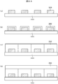
図16~図18を参照して、実施例9の固体微粒子質量測定装置の構成について説明する。
図16(A)、図17に示すように、実施例8の固体微粒子質量測定装置では、実施例8(図14参照)と比べて、格子状電極108が間引かれており、かつ一部が塗りつぶされている。 The configuration of the solid particulate matter mass measurement device of the ninth embodiment will be described with reference to FIGS. 16 to 18.
As shown in FIG. 16A and FIG. 17, in the solid fine particle mass measuring apparatus of the eighth embodiment, thegrid electrode 108 is thinned and partially compared to the eighth embodiment (see FIG. 14). Is filled.
図16(A)、図17に示すように、実施例8の固体微粒子質量測定装置では、実施例8(図14参照)と比べて、格子状電極108が間引かれており、かつ一部が塗りつぶされている。 The configuration of the solid particulate matter mass measurement device of the ninth embodiment will be described with reference to FIGS. 16 to 18.
As shown in FIG. 16A and FIG. 17, in the solid fine particle mass measuring apparatus of the eighth embodiment, the
このような構成では、使用する領域で感度を一定にすることができる。例えば、図14(B)のA~Eの領域を使用したい場合には、格子状電極108の間引き及び塗りつぶしの度合いにより、図16(B)に示すように、領域A~Eで感度を一定にすることができる。
In such a configuration, the sensitivity can be made constant in the region of use. For example, when it is desired to use the areas A to E in FIG. 14B, the sensitivity is constant in the areas A to E as shown in FIG. Can be
また、例えば、図14(B)のB~Dの領域を使用したい場合には、格子状電極108の間引き及び塗りつぶしの度合いにより、図16(C)に示すように、領域B~Dで感度を一定にすることができる。
ここで、格子状電極108の間引き及び塗りつぶしの度合いとして、図16に示すパターンや、図17に示すパターンや、図18に示すパターンを適宜選択して使用する。 Also, for example, when it is desired to use the regions B to D in FIG. 14B, the sensitivity in the regions B to D as shown in FIG. 16C depending on the degree of thinning and filling of thegrid electrode 108 Can be fixed.
Here, a pattern shown in FIG. 16, a pattern shown in FIG. 17, or a pattern shown in FIG. 18 is appropriately selected and used as the degree of thinning and filling of thegrid electrode 108.
ここで、格子状電極108の間引き及び塗りつぶしの度合いとして、図16に示すパターンや、図17に示すパターンや、図18に示すパターンを適宜選択して使用する。 Also, for example, when it is desired to use the regions B to D in FIG. 14B, the sensitivity in the regions B to D as shown in FIG. 16C depending on the degree of thinning and filling of the
Here, a pattern shown in FIG. 16, a pattern shown in FIG. 17, or a pattern shown in FIG. 18 is appropriately selected and used as the degree of thinning and filling of the
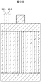
図19、図20を参照して、実施例10の固体微粒子質量測定装置の構成について説明する。
実施例2では、図2に示すように、固体微粒子付着領域109は表面弾性波伝搬領域109に設けられた第1の金属電極106により形成される。
実施例10では、図19に示すように、第1の金属電極106に対してヒータ及び抵抗温度計190を配置する。 The configuration of the solid particulate matter mass measurement device of the tenth embodiment will be described with reference to FIGS. 19 and 20. FIG.
In Example 2, as shown in FIG. 2, the solid fineparticle adhesion area 109 is formed by the first metal electrode 106 provided in the surface acoustic wave propagation area 109.
In the tenth embodiment, as shown in FIG. 19, a heater andresistance thermometer 190 are disposed for the first metal electrode 106.
実施例2では、図2に示すように、固体微粒子付着領域109は表面弾性波伝搬領域109に設けられた第1の金属電極106により形成される。
実施例10では、図19に示すように、第1の金属電極106に対してヒータ及び抵抗温度計190を配置する。 The configuration of the solid particulate matter mass measurement device of the tenth embodiment will be described with reference to FIGS. 19 and 20. FIG.
In Example 2, as shown in FIG. 2, the solid fine
In the tenth embodiment, as shown in FIG. 19, a heater and
このような構成の下、固体微粒子付着領域109として機能する第1の金属電極106をヒータ及び抵抗温度計190により高温(例えば600℃以上)に加熱して、第1の金属電極106に付着した固体微粒子(PM)を除去する。これにより、飽和領域(例えば、図11(C)の領域E)に達したとき、リフレッシュが可能となる。
Under such a configuration, the first metal electrode 106 functioning as the solid fine particle adhesion region 109 is heated to a high temperature (for example, 600 ° C. or higher) by the heater and resistance thermometer 190 and adhered to the first metal electrode 106 Remove solid particulates (PM). Thus, when the saturation region (for example, the region E in FIG. 11C) is reached, the refresh is possible.
尚、図19では、ヒータ及び抵抗温度計190を一体に形成したが、ヒータと抵抗温度計を分けて形成しても良い。
また、図20に示すように、セラミック基板195に接着層196とSAW素子197を実装し、セラミック基板195と接着層196の間にヒータ及び抵抗温度計190を配置しても良い。 Although the heater and theresistance thermometer 190 are integrally formed in FIG. 19, the heater and the resistance thermometer may be separately formed.
Further, as shown in FIG. 20, theadhesive layer 196 and the SAW element 197 may be mounted on the ceramic substrate 195, and the heater and resistance thermometer 190 may be disposed between the ceramic substrate 195 and the adhesive layer 196.
また、図20に示すように、セラミック基板195に接着層196とSAW素子197を実装し、セラミック基板195と接着層196の間にヒータ及び抵抗温度計190を配置しても良い。 Although the heater and the
Further, as shown in FIG. 20, the
次に、図21のフローチャートを参照して、実施例10の固体微粒子質量測定装置の動作について説明する。
最初に、センサの出力(位相または遅延時間)を計測(1)する(S210)し、PM付着量の絶対値を求める(S211)。
次に、センサの出力を計測(2)する(S212)。
次に、センサの出力の計測(2)結果から、飽和状態になっているかを判定する(S213)。 Next, with reference to the flowchart of FIG. 21, the operation of the solid particulate matter mass measurement device of the tenth embodiment will be described.
First, the output (phase or delay time) of the sensor is measured (1) (S210), and the absolute value of the PM adhesion amount is determined (S211).
Next, the output of the sensor is measured (2) (S212).
Next, from the measurement (2) result of the output of the sensor, it is determined whether or not it is in a saturated state (S213).
飽和状態になっている場合には、所望の温度になるように、ヒータ及び抵抗温度計190に通電する(S214)。
ヒータ及び抵抗温度計190を通電後、リフレッシュを行い(S215)、通電をオフする(S216)。
S213で飽和状態になっていない場合には、出力(1)と出力(2)の差から、単位時間当たりのPM付着量を算出する(S217)。 If the temperature is saturated, the heater andresistance thermometer 190 are energized to reach a desired temperature (S214).
After energizing the heater andresistance thermometer 190, refresh is performed (S215), and the energization is turned off (S216).
If the saturated state is not obtained in S213, the PM adhesion amount per unit time is calculated from the difference between the output (1) and the output (2) (S217).
ヒータ及び抵抗温度計190を通電後、リフレッシュを行い(S215)、通電をオフする(S216)。
S213で飽和状態になっていない場合には、出力(1)と出力(2)の差から、単位時間当たりのPM付着量を算出する(S217)。 If the temperature is saturated, the heater and
After energizing the heater and
If the saturated state is not obtained in S213, the PM adhesion amount per unit time is calculated from the difference between the output (1) and the output (2) (S217).
最後に、単位時間当たりのPM付着量を出力(OUT)する(S218)。
PM付着量を係数倍することで、エンジンのPM排出量が分かる。そして、センサの出力として、図8に示す実施例5の参照素子122との出力差を使うと、温度依存性の影響を除去できるので好ましい。 Finally, the PM adhesion amount per unit time is output (OUT) (S218).
The PM emission amount of the engine can be determined by multiplying the PM adhesion amount by a factor. Then, it is preferable to use the output difference from thereference element 122 of the fifth embodiment shown in FIG. 8 as the output of the sensor, because the influence of the temperature dependency can be eliminated.
PM付着量を係数倍することで、エンジンのPM排出量が分かる。そして、センサの出力として、図8に示す実施例5の参照素子122との出力差を使うと、温度依存性の影響を除去できるので好ましい。 Finally, the PM adhesion amount per unit time is output (OUT) (S218).
The PM emission amount of the engine can be determined by multiplying the PM adhesion amount by a factor. Then, it is preferable to use the output difference from the
図22を参照して、実施例11の固体微粒子質量測定装置の構成について説明する。
実施例11は、図16に示す実施例9の固体微粒子質量測定装置の変形例である。図22(A)は上面図、図22(B)は格子状金属電極108の中心近傍の断面図である。
図22(A)、(B)に示すように、実施例11の固体微粒子質量測定装置では、金属230の上に絶縁膜220が形成されている。このように、絶縁膜220を形成することにより、耐熱性を向上させて断線を防ぎ、安全にリフレッシュを行うことができる。 The configuration of the solid particulate matter mass measurement device of the eleventh embodiment will be described with reference to FIG.
The eleventh embodiment is a modification of the solid particulate matter mass measurement device of the ninth embodiment shown in FIG. FIG. 22A is a top view, and FIG. 22B is a cross-sectional view of the vicinity of the center of the grid-like metal electrode 108.
As shown in FIGS. 22A and 22B, in the solid fine particle mass measuring device of the eleventh embodiment, the insulatingfilm 220 is formed on the metal 230. By thus forming the insulating film 220, heat resistance can be improved, disconnection can be prevented, and refreshing can be performed safely.
実施例11は、図16に示す実施例9の固体微粒子質量測定装置の変形例である。図22(A)は上面図、図22(B)は格子状金属電極108の中心近傍の断面図である。
図22(A)、(B)に示すように、実施例11の固体微粒子質量測定装置では、金属230の上に絶縁膜220が形成されている。このように、絶縁膜220を形成することにより、耐熱性を向上させて断線を防ぎ、安全にリフレッシュを行うことができる。 The configuration of the solid particulate matter mass measurement device of the eleventh embodiment will be described with reference to FIG.
The eleventh embodiment is a modification of the solid particulate matter mass measurement device of the ninth embodiment shown in FIG. FIG. 22A is a top view, and FIG. 22B is a cross-sectional view of the vicinity of the center of the grid-
As shown in FIGS. 22A and 22B, in the solid fine particle mass measuring device of the eleventh embodiment, the insulating
図23を参照して、実施例12の固体微粒子質量測定装置の構成について説明する。
実施例12は、図11に示す実施例6の固体微粒子質量測定装置の変形例である。
図23(A)に示すように、実施例12の固体微粒子質量測定装置では、圧電基板111(ランガサイト)は長方形である必要はなく、例えば平行四辺形でも良い。
このような構成では、出力電極104を通過した表面弾性波(SAW)1が出力電極104を再通過することを防ぎ感度が安定する。 The configuration of the solid particulate matter mass measurement device of the twelfth embodiment will be described with reference to FIG.
A twelfth embodiment is a modification of the solid particulate matter mass measurement device of the sixth embodiment shown in FIG.
As shown in FIG. 23A, in the solid particle mass measuring device of the twelfth embodiment, the piezoelectric substrate 111 (langasite) does not have to be rectangular, and may be, for example, a parallelogram.
In such a configuration, the surface acoustic wave (SAW) 1 that has passed through theoutput electrode 104 is prevented from passing again through the output electrode 104, and the sensitivity is stabilized.
実施例12は、図11に示す実施例6の固体微粒子質量測定装置の変形例である。
図23(A)に示すように、実施例12の固体微粒子質量測定装置では、圧電基板111(ランガサイト)は長方形である必要はなく、例えば平行四辺形でも良い。
このような構成では、出力電極104を通過した表面弾性波(SAW)1が出力電極104を再通過することを防ぎ感度が安定する。 The configuration of the solid particulate matter mass measurement device of the twelfth embodiment will be described with reference to FIG.
A twelfth embodiment is a modification of the solid particulate matter mass measurement device of the sixth embodiment shown in FIG.
As shown in FIG. 23A, in the solid particle mass measuring device of the twelfth embodiment, the piezoelectric substrate 111 (langasite) does not have to be rectangular, and may be, for example, a parallelogram.
In such a configuration, the surface acoustic wave (SAW) 1 that has passed through the
ここで、表面弾性波(SAW)1が出力電極104を再通過した場合の感度を図23(B)に示す。図23(B)に示すように、再通過した場合の感度は一定しないことが分かる。実施例12では、再通過した場合の感度が一定になる。
Here, FIG. 23B shows the sensitivity when the surface acoustic wave (SAW) 1 passes through the output electrode 104 again. As shown in FIG. 23B, it can be seen that the sensitivity in the case of repassing is not constant. In Example 12, the sensitivity in the case of repassing becomes constant.
図24を参照して、実施例13の固体微粒子質量測定装置の構成について説明する。
図24に示すように、実施例13の固体微粒子質量測定装置では、反射器240を設けて入出力電極を兼用する。
このような構成では、表面弾性波1が固体微粒子付着領域109を2回通過するので感度が2倍となる。 The configuration of the solid particulate matter mass measurement device of the thirteenth embodiment will be described with reference to FIG.
As shown in FIG. 24, in the solid particulate matter mass measurement device of the thirteenth embodiment, areflector 240 is provided to double as an input / output electrode.
In such a configuration, since the surfaceacoustic wave 1 passes through the solid fine particle adhesion region 109 twice, the sensitivity is doubled.
図24に示すように、実施例13の固体微粒子質量測定装置では、反射器240を設けて入出力電極を兼用する。
このような構成では、表面弾性波1が固体微粒子付着領域109を2回通過するので感度が2倍となる。 The configuration of the solid particulate matter mass measurement device of the thirteenth embodiment will be described with reference to FIG.
As shown in FIG. 24, in the solid particulate matter mass measurement device of the thirteenth embodiment, a
In such a configuration, since the surface
図25のフローチャートを参照して、実施例13の固体微粒子質量測定装置の動作について説明する。
最初に、スイッチ1(241)、スイッチ2(242)を信号発生回路90に接続する(S250)。
次に、信号発生回路90から信号を出力する(S251)。
次に、入力電極(櫛型電極)103で表面弾性波(SAW)1を励振する(S252)。
次に、表面弾性波(SAW)1が固体微粒子付着領域109を通過して、反射器240で反射され、再度、固体微粒子付着領域109を通過する(S253)。
次に、スイッチ1(241)、スイッチ2(242)を信号検出回路91に接続する(S254)。
次に、信号検出回路91で遅延時間及び位相量を計測する(S255)。
最後に、PM排出量を出力する(S256)。 The operation of the solid particulate matter mass measurement device of the thirteenth embodiment will be described with reference to the flowchart of FIG.
First, the switch 1 (241) and the switch 2 (242) are connected to the signal generation circuit 90 (S250).
Next, thesignal generation circuit 90 outputs a signal (S251).
Next, the surface acoustic wave (SAW) 1 is excited by the input electrode (comb electrode) 103 (S 252).
Next, the surface acoustic wave (SAW) 1 passes through the solid fineparticle adhesion area 109, is reflected by the reflector 240, and passes through the solid fine particle adhesion area 109 again (S253).
Next, the switch 1 (241) and the switch 2 (242) are connected to the signal detection circuit 91 (S254).
Next, thesignal detection circuit 91 measures the delay time and the phase amount (S255).
Finally, the PM emission amount is output (S256).
最初に、スイッチ1(241)、スイッチ2(242)を信号発生回路90に接続する(S250)。
次に、信号発生回路90から信号を出力する(S251)。
次に、入力電極(櫛型電極)103で表面弾性波(SAW)1を励振する(S252)。
次に、表面弾性波(SAW)1が固体微粒子付着領域109を通過して、反射器240で反射され、再度、固体微粒子付着領域109を通過する(S253)。
次に、スイッチ1(241)、スイッチ2(242)を信号検出回路91に接続する(S254)。
次に、信号検出回路91で遅延時間及び位相量を計測する(S255)。
最後に、PM排出量を出力する(S256)。 The operation of the solid particulate matter mass measurement device of the thirteenth embodiment will be described with reference to the flowchart of FIG.
First, the switch 1 (241) and the switch 2 (242) are connected to the signal generation circuit 90 (S250).
Next, the
Next, the surface acoustic wave (SAW) 1 is excited by the input electrode (comb electrode) 103 (S 252).
Next, the surface acoustic wave (SAW) 1 passes through the solid fine
Next, the switch 1 (241) and the switch 2 (242) are connected to the signal detection circuit 91 (S254).
Next, the
Finally, the PM emission amount is output (S256).
このように、実施例13によれば、表面弾性波1が固体微粒子付着領域109を2回通過するので感度を2倍にすることができる。
Thus, according to Example 13, since the surface acoustic wave 1 passes through the solid fine particle adhesion region 109 twice, the sensitivity can be doubled.
実施例14は、図14に示す固体微粒子質量測定装置と図16に示す固体微粒子質量測定装置とを使用してDPF(Diesel Particulate Filter)を構成する。
In Example 14, a DPF (Diesel Particulate Filter) is configured using the solid particle mass measuring device shown in FIG. 14 and the solid particle mass measuring device shown in FIG.
図26に示すように、図14の低感度PMセンサ262をディーゼルエンジン261とDPF264の間に配置し、図16の高感度PMセンサ263をDPF264の後方に配置する。
このような構成では、PM量が大きい場所が低感度になり飽和が難しくなる。一方、PM量が小さい場所が高感度になり高感度センシングが可能になる。 As shown in FIG. 26, the lowsensitivity PM sensor 262 of FIG. 14 is disposed between the diesel engine 261 and the DPF 264, and the high sensitivity PM sensor 263 of FIG. 16 is disposed behind the DPF 264.
In such a configuration, the location where the amount of PM is large becomes low in sensitivity and saturation becomes difficult. On the other hand, a place where the amount of PM is small has high sensitivity and high sensitivity sensing becomes possible.
このような構成では、PM量が大きい場所が低感度になり飽和が難しくなる。一方、PM量が小さい場所が高感度になり高感度センシングが可能になる。 As shown in FIG. 26, the low
In such a configuration, the location where the amount of PM is large becomes low in sensitivity and saturation becomes difficult. On the other hand, a place where the amount of PM is small has high sensitivity and high sensitivity sensing becomes possible.
上記実施例によれば、伝搬路である表面弾性波伝搬領域105上に固体微粒子を収集し付着させる固体微粒子付着領域109を設けることにより、大気中に含まれる固体微粒子の含有量(質量)を高精度に検出することができる。
According to the above embodiment, by providing the solid particle adhesion region 109 for collecting and adhering solid particles on the surface acoustic wave propagation region 105 which is a propagation path, the content (mass) of the solid particles contained in the atmosphere can be determined. It can be detected with high accuracy.
1 表面弾性波
11 GND電極
90 信号発生回路
91 信号検出回路
100 電極指
101 バスバー
102 電気端子
103 櫛型電極
104 櫛型電極
105 表面弾性波伝搬領域
106 金属電極
107 金属電極
108 格子状金属電極
109 固体微粒子付着領域
111 圧電基板
112 絶縁膜
113 固体微粒子付着防止マスク
114 格子状電極の幅
115 格子状電極間の距離
116 固体微粒子付着防止マスクの開口部
132 櫛形電極の幅
133 櫛形電極間の距離
201 ガス導入路
202 固体微粒子 1 surfaceacoustic wave 11 GND electrode 90 signal generation circuit 91 signal detection circuit 100 electrode finger 101 bus bar 102 electric terminal 103 comb electrode 104 comb electrode 105 surface acoustic wave propagation area 106 metal electrode 107 metal electrode 108 grid-like metal electrode 109 solid Fine particle adhesion area 111 Piezoelectric substrate 112 Insulating film 113 Solid fine particle adhesion prevention mask 114 Width of grid electrode 115 Distance between lattice electrodes 116 Opening of solid fine particle adhesion prevention mask 132 Width of comb electrode 133 Distance between comb electrodes 201 Gas Introduction path 202 solid particles
11 GND電極
90 信号発生回路
91 信号検出回路
100 電極指
101 バスバー
102 電気端子
103 櫛型電極
104 櫛型電極
105 表面弾性波伝搬領域
106 金属電極
107 金属電極
108 格子状金属電極
109 固体微粒子付着領域
111 圧電基板
112 絶縁膜
113 固体微粒子付着防止マスク
114 格子状電極の幅
115 格子状電極間の距離
116 固体微粒子付着防止マスクの開口部
132 櫛形電極の幅
133 櫛形電極間の距離
201 ガス導入路
202 固体微粒子 1 surface
Claims (15)
- 気体中に含まれる固体微粒子の含有量を測定する固体微粒子質量測定装置であって、
圧電基板と、
前記圧電基板の一端に設けられ、表面弾性波を励起する入力電極と、
前記圧電基板の他端に設けられ、前記入力電極で励起されて前記圧電基板上の表面弾性波伝搬領域を伝搬する前記表面弾性波を受信する出力電極と、
前記表面弾性波伝搬領域に設けられ、前記固体微粒子を付着させる固体微粒子付着領域と、
前記固体微粒子付着領域に付着した前記固体微粒子の付着量を検出する固体微粒子付着量検出部と、
を有することを特徴とする固体微粒子質量測定装置。 A solid particle mass measuring apparatus for measuring the content of solid particles contained in a gas, comprising:
A piezoelectric substrate,
An input electrode provided at one end of the piezoelectric substrate to excite surface acoustic waves;
An output electrode provided at the other end of the piezoelectric substrate and receiving the surface acoustic wave which is excited by the input electrode and propagates a surface acoustic wave propagation region on the piezoelectric substrate;
A solid particle adhesion region provided in the surface acoustic wave propagation region and adhering the solid particles;
A solid particle adhesion amount detection unit that detects the adhesion amount of the solid particles adhered to the solid particle adhesion region;
A solid particle mass measuring device characterized by having. - 前記固体微粒子付着量検出部は、
前記固体微粒子付着領域に付着した前記固体微粒子と前記表面弾性波との相互作用により、前記表面弾性波が前記表面弾性波伝搬領域を伝搬する伝搬速度が変化することにより生じた前記表面弾性波の位相の変化を前記出力電極で検出することにより、前記固体微粒子の付着量を検出することを特徴とする請求項1に記載の固体微粒子質量測定装置。 The solid particle adhesion amount detection unit
The interaction of the solid fine particles attached to the solid fine particle adhering area and the surface elastic wave causes the surface elastic wave to propagate in the surface elastic wave propagation area, thereby changing the propagation speed of the surface elastic wave The solid fine particle mass measuring apparatus according to claim 1, wherein the adhesion amount of the solid fine particles is detected by detecting a change in phase with the output electrode. - 前記入力電極及び前記出力電極は、前記表面弾性波の伝搬方向に対して垂直方向に対向して配置された櫛型の電極により形成されていることを特徴とする請求項1に記載の固体微粒子質量測定装置。 The solid fine particle according to claim 1, wherein the input electrode and the output electrode are formed of comb-shaped electrodes disposed to face each other in a direction perpendicular to the propagation direction of the surface acoustic wave. Mass measuring device.
- 前記櫛型の電極は、複数の電極指を有し、
前記電極指の幅及び隣接する前記電極指の間の距離は、前記表面弾性波の波長の1/4であることを特徴とする請求項1に記載の固体微粒子質量測定装置。 The comb-shaped electrode has a plurality of electrode fingers,
The solid particle mass measuring device according to claim 1, wherein a width of the electrode finger and a distance between the adjacent electrode fingers are 1/4 of a wavelength of the surface acoustic wave. - 前記固体微粒子付着領域は、前記表面弾性波伝搬領域に設けられた第1の金属電極により形成され、
前記第1の金属電極の上部には、前記第1の金属電極と対向して第2の金属電極が設けられ、
前記第1の金属電極と前記第2の金属電極との間に電圧を印加することにより前記第1の金属電極に前記固体微粒子を付着させることを特徴とする請求項1に記載の固体微粒子質量測定装置。 The solid fine particle adhesion area is formed by a first metal electrode provided in the surface acoustic wave propagation area,
A second metal electrode is provided on the top of the first metal electrode to face the first metal electrode,
The solid particle mass according to claim 1, wherein the solid particles are attached to the first metal electrode by applying a voltage between the first metal electrode and the second metal electrode. measuring device. - 前記第1の金属電極は、複数の格子状電極により形成され、
前記固体微粒子は、複数の前記格子状電極の周辺に付着することを特徴とする請求項5に記載の固体微粒子質量測定装置。 The first metal electrode is formed of a plurality of grid-like electrodes,
The said solid particulates adhere on the periphery of several said grid | lattice-like electrodes, The solid particulate mass measuring apparatus of Claim 5 characterized by the above-mentioned. - 前記格子状電極の幅及び隣接する前記格子状電極の間隔は、前記表面弾性波の波長より小さいことを特徴とする請求項6に記載の固体微粒子質量測定装置。 7. The solid particle mass measuring device according to claim 6, wherein a width of the grid electrode and an interval between the adjacent grid electrodes are smaller than a wavelength of the surface acoustic wave.
- 前記格子状電極の幅及び隣接する前記格子状電極の間隔は、前記表面弾性波の波長の1/2以下であることを特徴とする請求項7に記載の固体微粒子質量測定装置。 The solid particle mass measuring device according to claim 7, wherein the width of the grid electrode and the interval between the adjacent grid electrodes are equal to or less than 1/2 of the wavelength of the surface acoustic wave.
- 複数の前記格子状電極は間引かれており、
前記固体微粒子は電界に引き付けられて段差を設けながら間引かれた複数の前記格子状電極上に付着することを特徴とする請求項6に記載の固体微粒子質量測定装置。 The plurality of grid electrodes are thinned out,
7. The solid particle mass measuring device according to claim 6, wherein the solid particles are attracted to an electric field and attached onto the plurality of grid electrodes which are thinned while providing a level difference. - 前記第1の金属電極を加熱することにより前記第1の金属電極に付着した前記固体微粒子を除去するヒータを更に有することを特徴とする請求項6に記載の固体微粒子質量測定装置。 The solid particle mass measuring apparatus according to claim 6, further comprising a heater for removing the solid particles attached to the first metal electrode by heating the first metal electrode.
- 前記固体微粒子付着領域は平坦膜により形成され、
前記固体微粒子は、前記平坦膜に印加されたDCバイアス電圧の電界に引き付けられて前記平坦膜に一様に付着することを特徴とする請求項1に記載の固体微粒子質量測定装置。 The solid fine particle adhesion region is formed by a flat film,
The solid particle mass measuring apparatus according to claim 1, wherein the solid particles are attracted to an electric field of a DC bias voltage applied to the flat film and uniformly attached to the flat film. - 前記表面弾性波伝搬領域へ前記固体微粒子を含む前記気体を導入する導入路を更に有することを特徴とする請求項1に記載の固体微粒子質量測定装置。 The solid particle mass measuring device according to claim 1, further comprising an introduction path for introducing the gas containing the solid particles into the surface acoustic wave propagation region.
- 請求項1に記載された固体微粒子質量測定装置を一対配置し、
一の固体微粒子質量測定装置を測定素子として用い、
他の固体微粒子質量測定装置を参照素子として用い、
前記参照素子の前記固体微粒子付着領域には、前記固体微粒子が付着するのを阻止するためのマスクが設けられ、
前記固体微粒子付着量検出部は、前記測定素子と前記参照素子の前記出力電極でそれぞれ受信される前記表面弾性波の特性を比較することにより、前記固体微粒子の前記付着量を検出することを特徴とする固体微粒子質量測定装置。 A pair of solid particle mass measuring devices according to claim 1 are arranged,
Using a single solid particle mass measuring device as a measuring element,
Another solid particulate mass measuring device is used as a reference element,
The solid particulate matter adhesion region of the reference element is provided with a mask for preventing the solid particulate matter from adhering thereto.
The solid particle adhesion amount detection unit is characterized in that the adhesion amount of the solid particles is detected by comparing the characteristics of the surface acoustic wave respectively received by the output element of the measurement element and the reference element. Solid particle mass measuring device to be. - 前記測定用素子の前記固体微粒子付着領域は、絶縁膜の窓が開口されており、
前記参照素子の前記固体微粒子付着領域は、前記絶縁膜で覆われていることを特徴とする請求項13に記載の固体微粒子質量測定装置。 In the solid fine particle adhesion region of the measurement element, a window of an insulating film is opened,
The solid particulate matter mass measuring device according to claim 13, wherein the solid particulate matter adhering region of the reference element is covered with the insulating film. - 前記入力電極及び出力電極は、白金とチタンとの2層構造により形成されていることを特徴とする請求項1に記載の固体微粒子質量測定装置。 The solid particle mass measuring device according to claim 1, wherein the input electrode and the output electrode are formed by a two-layer structure of platinum and titanium.
Applications Claiming Priority (2)
| Application Number | Priority Date | Filing Date | Title |
|---|---|---|---|
| JP2017220689A JP2019090742A (en) | 2017-11-16 | 2017-11-16 | Solid particles mass measurement device |
| JP2017-220689 | 2017-11-16 |
Publications (1)
| Publication Number | Publication Date |
|---|---|
| WO2019097769A1 true WO2019097769A1 (en) | 2019-05-23 |
Family
ID=66540177
Family Applications (1)
| Application Number | Title | Priority Date | Filing Date |
|---|---|---|---|
| PCT/JP2018/028452 WO2019097769A1 (en) | 2017-11-16 | 2018-07-30 | Solid microparticle mass measurement device |
Country Status (2)
| Country | Link |
|---|---|
| JP (1) | JP2019090742A (en) |
| WO (1) | WO2019097769A1 (en) |
Cited By (2)
| Publication number | Priority date | Publication date | Assignee | Title |
|---|---|---|---|---|
| WO2020241867A1 (en) * | 2019-05-31 | 2020-12-03 | 京セラ株式会社 | Sensor device |
| EP4016088A1 (en) * | 2020-12-21 | 2022-06-22 | Hamilton Sundstrand Corporation | Surface acoustic wave sensors for air data probes |
Citations (8)
| Publication number | Priority date | Publication date | Assignee | Title |
|---|---|---|---|---|
| GB2371362A (en) * | 2001-01-18 | 2002-07-24 | Univ Nottingham Trent | Monitoring apparatus and method for detecting particles in a gas stream using ionisation means and a SAW detector |
| JP2003502616A (en) * | 1998-11-04 | 2003-01-21 | ローベルト ボツシユ ゲゼルシヤフト ミツト ベシユレンクテル ハフツング | Sensor device and method for detecting concentration and viscosity of liquid |
| JP2004069686A (en) * | 2002-06-24 | 2004-03-04 | Particle Measuring Syst Inc | System and method for monitoring molecular contamination |
| JP2008275503A (en) * | 2007-05-01 | 2008-11-13 | Japan Radio Co Ltd | Density measurement device |
| JP2009109261A (en) * | 2007-10-29 | 2009-05-21 | Tama Tlo Kk | Surface acoustic wave gas sensor device |
| WO2013108608A1 (en) * | 2012-01-20 | 2013-07-25 | パナソニック株式会社 | Elastic wave sensor |
| JP2015081861A (en) * | 2013-10-23 | 2015-04-27 | ファインクリスタル株式会社 | Surface acoustic wave sensor and surface acoustic wave sensor device |
| JP2015210080A (en) * | 2014-04-23 | 2015-11-24 | 日本無線株式会社 | Surface acoustic wave sensor |
-
2017
- 2017-11-16 JP JP2017220689A patent/JP2019090742A/en active Pending
-
2018
- 2018-07-30 WO PCT/JP2018/028452 patent/WO2019097769A1/en active Application Filing
Patent Citations (8)
| Publication number | Priority date | Publication date | Assignee | Title |
|---|---|---|---|---|
| JP2003502616A (en) * | 1998-11-04 | 2003-01-21 | ローベルト ボツシユ ゲゼルシヤフト ミツト ベシユレンクテル ハフツング | Sensor device and method for detecting concentration and viscosity of liquid |
| GB2371362A (en) * | 2001-01-18 | 2002-07-24 | Univ Nottingham Trent | Monitoring apparatus and method for detecting particles in a gas stream using ionisation means and a SAW detector |
| JP2004069686A (en) * | 2002-06-24 | 2004-03-04 | Particle Measuring Syst Inc | System and method for monitoring molecular contamination |
| JP2008275503A (en) * | 2007-05-01 | 2008-11-13 | Japan Radio Co Ltd | Density measurement device |
| JP2009109261A (en) * | 2007-10-29 | 2009-05-21 | Tama Tlo Kk | Surface acoustic wave gas sensor device |
| WO2013108608A1 (en) * | 2012-01-20 | 2013-07-25 | パナソニック株式会社 | Elastic wave sensor |
| JP2015081861A (en) * | 2013-10-23 | 2015-04-27 | ファインクリスタル株式会社 | Surface acoustic wave sensor and surface acoustic wave sensor device |
| JP2015210080A (en) * | 2014-04-23 | 2015-11-24 | 日本無線株式会社 | Surface acoustic wave sensor |
Cited By (6)
| Publication number | Priority date | Publication date | Assignee | Title |
|---|---|---|---|---|
| WO2020241867A1 (en) * | 2019-05-31 | 2020-12-03 | 京セラ株式会社 | Sensor device |
| JPWO2020241867A1 (en) * | 2019-05-31 | 2020-12-03 | ||
| CN113924483A (en) * | 2019-05-31 | 2022-01-11 | 京瓷株式会社 | Sensor device |
| JP7231725B2 (en) | 2019-05-31 | 2023-03-01 | 京セラ株式会社 | sensor device |
| EP4016088A1 (en) * | 2020-12-21 | 2022-06-22 | Hamilton Sundstrand Corporation | Surface acoustic wave sensors for air data probes |
| US11549914B2 (en) | 2020-12-21 | 2023-01-10 | Hamilton Sundstrand Corporation | Surface acoustic wave sensors for air data probes |
Also Published As
| Publication number | Publication date |
|---|---|
| JP2019090742A (en) | 2019-06-13 |
Similar Documents
| Publication | Publication Date | Title |
|---|---|---|
| US7285894B1 (en) | Surface acoustic wave devices for high temperature applications | |
| JP2013122439A (en) | Particulate matter sensor unit and method for manufacturing the same | |
| WO2019097769A1 (en) | Solid microparticle mass measurement device | |
| KR100706561B1 (en) | Method and device for operating a microacoustic sensor array | |
| CN110231095A (en) | A kind of phasmon surface acoustic wave resonance infrared sensor | |
| Giffney et al. | A surface acoustic wave ethanol sensor with zinc oxide nanorods | |
| JP6477120B2 (en) | Physical quantity sensor | |
| JP2004093574A (en) | Cantilever with force azimuth sensor for atomic force microscope | |
| KR100698439B1 (en) | Surface acoustic wave gas sensor for detecting volatile chemicals | |
| GB2371362A (en) | Monitoring apparatus and method for detecting particles in a gas stream using ionisation means and a SAW detector | |
| JP6558029B2 (en) | Surface acoustic wave device and physical quantity sensor using the same | |
| CA2549837A1 (en) | Sensor, sensor arrangement, and measuring method | |
| Priya et al. | A comparison of surface acoustic wave (SAW) delay line modelling techniques for sensor applications | |
| US20210265974A1 (en) | Film bulk acoustic sensors using thin ln-lt layer | |
| US7193352B1 (en) | Thin film bulk acoustic wave sensor suite | |
| JP6317567B2 (en) | Particle sensor | |
| JP2006337332A (en) | Material detector | |
| JP2020088539A (en) | Surface acoustic wave element and solid fine particles mass measuring instrument | |
| JP4003373B2 (en) | Surface acoustic wave sound velocity evaluation method | |
| Kumar et al. | Design and simulation of polyisobutylene/silicon nitride for detection of gas sensing | |
| JP2008180668A (en) | Lamb wave type high-frequency sensor device | |
| KR20160124384A (en) | Sensor element for sensing particle concentration | |
| JP2005265423A (en) | Surface elastic wave device | |
| Lim et al. | MEMS sensor for particulate matter measurement of exhaust gas | |
| JP3959532B2 (en) | Ultrasonic contact position detector |
Legal Events
| Date | Code | Title | Description |
|---|---|---|---|
| 121 | Ep: the epo has been informed by wipo that ep was designated in this application |
Ref document number: 18879696 Country of ref document: EP Kind code of ref document: A1 |
|
| NENP | Non-entry into the national phase |
Ref country code: DE |
|
| 122 | Ep: pct application non-entry in european phase |
Ref document number: 18879696 Country of ref document: EP Kind code of ref document: A1 |