WO2019091348A1 - Fpga云主机开发方法和系统 - Google Patents
Fpga云主机开发方法和系统 Download PDFInfo
- Publication number
- WO2019091348A1 WO2019091348A1 PCT/CN2018/113901 CN2018113901W WO2019091348A1 WO 2019091348 A1 WO2019091348 A1 WO 2019091348A1 CN 2018113901 W CN2018113901 W CN 2018113901W WO 2019091348 A1 WO2019091348 A1 WO 2019091348A1
- Authority
- WO
- WIPO (PCT)
- Prior art keywords
- development
- file
- fpga
- management platform
- programming
- Prior art date
- Legal status (The legal status is an assumption and is not a legal conclusion. Google has not performed a legal analysis and makes no representation as to the accuracy of the status listed.)
- Ceased
Links
Images


Classifications
-
- G—PHYSICS
- G06—COMPUTING OR CALCULATING; COUNTING
- G06F—ELECTRIC DIGITAL DATA PROCESSING
- G06F21/00—Security arrangements for protecting computers, components thereof, programs or data against unauthorised activity
- G06F21/50—Monitoring users, programs or devices to maintain the integrity of platforms, e.g. of processors, firmware or operating systems
- G06F21/51—Monitoring users, programs or devices to maintain the integrity of platforms, e.g. of processors, firmware or operating systems at application loading time, e.g. accepting, rejecting, starting or inhibiting executable software based on integrity or source reliability
-
- G—PHYSICS
- G06—COMPUTING OR CALCULATING; COUNTING
- G06F—ELECTRIC DIGITAL DATA PROCESSING
- G06F9/00—Arrangements for program control, e.g. control units
- G06F9/06—Arrangements for program control, e.g. control units using stored programs, i.e. using an internal store of processing equipment to receive or retain programs
- G06F9/44—Arrangements for executing specific programs
- G06F9/455—Emulation; Interpretation; Software simulation, e.g. virtualisation or emulation of application or operating system execution engines
- G06F9/45533—Hypervisors; Virtual machine monitors
- G06F9/45558—Hypervisor-specific management and integration aspects
-
- G—PHYSICS
- G06—COMPUTING OR CALCULATING; COUNTING
- G06F—ELECTRIC DIGITAL DATA PROCESSING
- G06F21/00—Security arrangements for protecting computers, components thereof, programs or data against unauthorised activity
- G06F21/10—Protecting distributed programs or content, e.g. vending or licensing of copyrighted material ; Digital rights management [DRM]
- G06F21/12—Protecting executable software
-
- G—PHYSICS
- G06—COMPUTING OR CALCULATING; COUNTING
- G06F—ELECTRIC DIGITAL DATA PROCESSING
- G06F21/00—Security arrangements for protecting computers, components thereof, programs or data against unauthorised activity
- G06F21/70—Protecting specific internal or peripheral components, in which the protection of a component leads to protection of the entire computer
- G06F21/71—Protecting specific internal or peripheral components, in which the protection of a component leads to protection of the entire computer to assure secure computing or processing of information
- G06F21/76—Protecting specific internal or peripheral components, in which the protection of a component leads to protection of the entire computer to assure secure computing or processing of information in application-specific integrated circuits [ASIC] or field-programmable devices, e.g. field-programmable gate arrays [FPGA] or programmable logic devices [PLD]
-
- G—PHYSICS
- G06—COMPUTING OR CALCULATING; COUNTING
- G06F—ELECTRIC DIGITAL DATA PROCESSING
- G06F30/00—Computer-aided design [CAD]
- G06F30/30—Circuit design
- G06F30/34—Circuit design for reconfigurable circuits, e.g. field programmable gate arrays [FPGA] or programmable logic devices [PLD]
-
- G—PHYSICS
- G06—COMPUTING OR CALCULATING; COUNTING
- G06F—ELECTRIC DIGITAL DATA PROCESSING
- G06F8/00—Arrangements for software engineering
- G06F8/30—Creation or generation of source code
-
- G—PHYSICS
- G06—COMPUTING OR CALCULATING; COUNTING
- G06F—ELECTRIC DIGITAL DATA PROCESSING
- G06F9/00—Arrangements for program control, e.g. control units
- G06F9/06—Arrangements for program control, e.g. control units using stored programs, i.e. using an internal store of processing equipment to receive or retain programs
- G06F9/44—Arrangements for executing specific programs
- G06F9/455—Emulation; Interpretation; Software simulation, e.g. virtualisation or emulation of application or operating system execution engines
- G06F9/45533—Hypervisors; Virtual machine monitors
-
- G—PHYSICS
- G06—COMPUTING OR CALCULATING; COUNTING
- G06F—ELECTRIC DIGITAL DATA PROCESSING
- G06F2111/00—Details relating to CAD techniques
- G06F2111/04—Constraint-based CAD
-
- G—PHYSICS
- G06—COMPUTING OR CALCULATING; COUNTING
- G06F—ELECTRIC DIGITAL DATA PROCESSING
- G06F2221/00—Indexing scheme relating to security arrangements for protecting computers, components thereof, programs or data against unauthorised activity
- G06F2221/03—Indexing scheme relating to G06F21/50, monitoring users, programs or devices to maintain the integrity of platforms
- G06F2221/033—Test or assess software
-
- G—PHYSICS
- G06—COMPUTING OR CALCULATING; COUNTING
- G06F—ELECTRIC DIGITAL DATA PROCESSING
- G06F8/00—Arrangements for software engineering
- G06F8/10—Requirements analysis; Specification techniques
Definitions
- the present invention relates to the field of Internet technologies, and in particular, to an FPGA cloud host development method and system.
- the FPGA cloud host or FPGA cloud server is a Field Programmable Gate Array (FPGA)-based computing service.
- FPGA Field Programmable Gate Array
- An FPGA cloud host can be understood as a normal cloud host (virtual machine) with an FPGA device. After purchasing the FPGA cloud host, if you want to use the FPGA, you need to develop the FPGA, get a burning file, and then burn this file into the FPGA. The FPGA implements the user-developed function.
- FPGA development environment and process are all developed and debugged by the user in the user's own environment, ie, the user side environment.
- the FPGA hardware is owned by the developer.
- FPGA development will face some new security challenges, both to ensure that users can develop FPGAs, and to ensure the security of cloud hosts and prevent malicious attacks.
- the embodiments of the present invention provide an FPGA cloud host development method and system, which are used to implement user development of an FPGA and prevent malicious attacks on the FPGA hardware.
- an embodiment of the present invention provides an FPGA cloud host development method, which is applied to a development management platform, and includes:
- the programming file obtained by the integrated processing is programmed into the FPGA.
- the method before the programming of the programming file obtained by the integrated processing into the FPGA, the method further includes:
- the programming file obtained by the integrated processing is programmed into the FPGA, including:
- the programming file corresponding to the programming indication is programmed into the FPGA in response to a programming indication triggered by the development device.
- an embodiment of the present invention provides an FPGA cloud host development method, which is applied to a development device, and includes:
- an embodiment of the present invention provides an FPGA cloud host development system, including:
- the development device is configured to design a design file, and upload the obtained design file to the development management platform, where the design file includes an actual constraint file corresponding to the FPGA;
- the development management platform is configured to perform legality detection on the actual constraint file. If the legality detection is passed, the design file is comprehensively processed, and the programming file obtained by the comprehensive processing is programmed into the FPGA. .
- the foregoing development management platform includes a processor and a memory for storing a program supporting the development management platform to execute the FPGA cloud host development method in the above first aspect, the processor being configured It is used to execute a program stored in the memory.
- the development management platform may also include a communication interface for the development management platform to communicate with other devices or communication networks.
- the embodiment of the invention provides a computer storage medium for storing computer software instructions used in the development management platform, which comprises a program for executing the FPGA cloud host development method in the first aspect.
- the foregoing development device includes a processor and a memory for storing a program supporting the development device to execute the FPGA cloud host development method in the second aspect, the processor configured to Used to execute programs stored in the memory.
- the development device can also include a communication interface for the communication device to communicate with other devices or communication networks.
- An embodiment of the present invention provides another computer storage medium for storing computer software instructions for developing a device, which includes a program for executing the FPGA cloud host development method in the second aspect.
- the FPGA cloud host development method and system provided by the embodiments of the present invention can be developed and designed by the user in the user-side development device to obtain a design file including the actual constraint file designed by the user for the FPGA, and then developed.
- the device uploads the design file to the development management platform.
- the development management platform ensures the security of the FPGA hardware by detecting the legality of the actual constraint file to avoid malicious attacks on the FPGA by changing the constraint file.
- Embodiment 1 is a schematic structural diagram of Embodiment 1 of an FPGA cloud host development system according to an embodiment of the present invention
- Embodiment 2 is a schematic structural diagram of Embodiment 2 of an FPGA cloud host development system according to an embodiment of the present invention
- FIG. 3 is a flowchart of Embodiment 1 of an FPGA cloud host development method according to an embodiment of the present disclosure
- Embodiment 4 is a flowchart of Embodiment 2 of an FPGA cloud host development method according to an embodiment of the present invention
- FIG. 5 is a schematic structural diagram of a development management platform according to an embodiment of the present invention.
- FIG. 6 is a schematic structural diagram of a development device according to an embodiment of the present invention.
- the words “if” and “if” as used herein may be interpreted to mean “when” or “when” or “in response to determining” or “in response to detecting.”
- the phrase “if determined” or “if detected (conditions or events stated)” may be interpreted as “when determined” or “in response to determination” or “when detected (stated condition or event) “Time” or “in response to a test (condition or event stated)”.
- FIG. 1 is a schematic structural diagram of Embodiment 1 of an FPGA cloud host development system according to an embodiment of the present invention. As shown in FIG. 1 , the system includes:
- Development equipment development management platform for remote communication connection with development equipment, and FPGA in FPGA cloud host.
- the development device is a user-side development device
- the development management platform is a network side or a cloud management platform, such as a server
- the development device and the development management platform can be understood as a relationship between the client and the server, that is, development.
- a client that supports user development can be set in the device.
- the development device is selected by the user and is a device for FPGA development. Alternatively, it may be a user offline device, such as a user's own computer or a virtual machine of the FPGA cloud host. In summary, the user can perform FPGA design and development related work in the device, including code writing, constraint design, and viewing comprehensive reports.
- the development device is used for the user to design the design file, and uploads the obtained design file to the development management platform, and the design file includes the actual constraint file corresponding to the FPGA.
- the development management platform is used for the legality detection of the actual constraint file. If the legality detection is passed, the design file is comprehensively processed, and the programming file obtained by the comprehensive processing is written into the FPGA.
- the development device is further configured to: receive a comprehensive report obtained by the integrated processing of the development management platform feedback; and send a programming instruction triggered by the comprehensive report to the development management platform.
- the development management platform is further configured to: feed back the comprehensive report obtained by the integrated processing to the development device; and program the above-mentioned programming file obtained by the integrated processing into the FPGA according to the above-mentioned programming instruction.
- the user writes the development files required by the user in the development device, and can compile and debug the written code, and finally form a design file, which can include the code written by the user and the actual
- the constraint file of the design is called the actual constraint file.
- the development device is further configured to: in response to the user-initiated startup development operation, send a development request to the development management platform to request the template constraint file.
- the development management platform is further configured to: send the template constraint file to the development device in response to the development request.
- the development management platform can be regarded as a unified management platform, which can assist different users to develop their respective FPGA cloud hosts. Therefore, the FPGA of the user can be provided in the development device.
- the setting item of the cloud host identification information when the user fills out the setting item and triggers a preset control or menu item, it is considered that the user triggers the startup development operation, and thus the development device can carry the development request sent to the development management platform.
- the identification information of the FPGA cloud host is such that the development management platform acquires the template constraint file of the FPGA in the FPGA cloud host based on the identification information, and feeds the obtained template constraint file to the development device.
- the identifier information of the FPGA cloud host may be used as a storage index, and the template constraint file corresponding to the FPGA of the plurality of FPGA cloud hosts is pre-stored.
- the function of the constraint file mentioned in the embodiment of the present invention is to define a chip pin to which an FPGA input and output signal is bound, that is, which pin of a certain signal is input from a certain signal of the FPGA, which tube of a certain signal from the FPGA Foot output.
- the constraint file defines various clock relationships, level standards, etc. in the FPGA, as well as some other constraints.
- the development management platform provides the template constraint file of the FPGA that the user needs to develop to the user through the development device, the user may modify, delete, add, etc. the template constraint file in the actual development process to form the actual design.
- the actual constraint file, and these operations will damage the FPGA itself and its surrounding hardware and software systems. Therefore, in order to ensure the security of the FPGA and prevent malicious attacks by users, the user submits the design file to the development management through the development device. After the platform, the development management platform needs to check the legality of the design file, specifically the legality detection of the actual constraint file in the design file.
- the development management platform may compare the template constraint file corresponding to the FPGA and the actual constraint file stored locally, and if the comparison result indicates that the template constraint file is consistent with the actual constraint file, determining that the actual constraint file passes the legal Sex detection.
- the template constraint file is consistent with the actual constraint file, that is, the various constraints included in the two files are the same, for example, the actual constraint file constrains a signal from a certain input of the FPGA, and if the template constraint file is also the same Constraining the signal from this pin input, then the two files have the same signal input constraints on the pin.
- the development management platform When the development management platform detects that the actual constraint file fails the legality detection, it may send an error prompt message to the development device, so that the user redesigns the design file.
- the design file uploaded by the development device can be comprehensively processed. In actual application, the integrated processing can be realized by using the existing comprehensive tool. Therefore, the development management platform is developed. A comprehensive tool is set in it.
- the comprehensive process includes three steps of analysis, synthesis and optimization.
- the design file can be described by the Hardware Description Language (HDL).
- the analysis uses the standard HDL grammar rules to analyze the HDL design files and correct the syntax errors.
- the synthesis is based on the selected FPGA structure and device.
- HDL and FPGA netlist files are logically integrated, and the design files are compiled into logical connection netlists composed of basic logic units such as AND gates, OR gates, NOT gates, RAMs, flip-flops, etc., instead of real gate-level circuits; optimization is The logic and area are logically optimized according to the user's design constraints to produce an optimized FPGA netlist file for use by the FPGA layout and routing tools. After the completion, a number of comprehensive reports and programming files can be output.
- the comprehensive report includes, for example, a time series report, a power report, a temperature report, etc., and the burn-in file can be analogized to the executable file compiled by the application.
- the report documents list the comprehensive status and comprehensive results, such as resource usage and integrated level information.
- IP cores that is, third-party intellectual property cores.
- These IP cores can be used by the user after authorization (purchase or other means).
- the IP core is a module that implements a certain function. Users can directly call an IP core in the application code to implement the corresponding function, which is equivalent to directly using an existing function module to avoid repeated development. .
- the third-party IP core can improve user development efficiency and avoid duplication of development, it is technically necessary to prevent users from exporting these IP cores to their own devices, because once they are spread out, users can provide IP cores to other unauthorized devices.
- the user uses or spreads to the Internet, etc., causing the problem of "one person to buy, all to use”. Therefore, in order to ensure the security of the use of the third-party IP core, it is not spread to the unauthorized user.
- a solution for protecting the third-party IP core is also provided.
- the development management platform may obtain a third-party IP core available for user authorization in advance, and store the third-party IP core locally, that is, the third-party IP core available to the user is stored in the development management platform.
- the setting item of the identifier information of the FPGA cloud host mentioned in the foregoing, the setting item of the user identifier may also be set in the development device, so that the development request may further include the user identifier, so that the development management platform may be based on the The user ID obtains the corresponding third-party IP core by maintaining a server with a third-party IP core.
- the third-party IP core is stored in the development management platform without being exposed to the user, that is, not provided to the user to develop the device.
- a third-party IP core When a third-party IP core needs to be used in the user development process, it can be used by calling. For example, the function description and input parameters of the third-party IP core available to the user can be provided to the user, so that the user can select the call according to the actual demand. Which third party IP core. Therefore, during the development process, when a third-party IP core needs to be invoked, it is only necessary to write the calling code of the third-party IP core in the design file, which is equivalent to declaring which third-party IP core needs to be called.
- the development management platform is also used to: if the third-party IP core is invoked in the design file, the third-party IP core and the design file to be called are comprehensively processed, and the comprehensive processing is obtained in advance.
- the defined non-sensitive comprehensive report is fed back to the development device, where the information of the called third-party IP core is not included in the non-sensitive comprehensive report.
- the input of the integrated processing includes the called third-party IP core in addition to the design file.
- the development management platform can determine whether the third-party IP core is invoked and which third-party IP core is invoked by analyzing whether the design file contains the name of the third-party IP core.
- the comprehensive report in the comprehensive result that can be reversed or extracted from the third-party IP core is not provided to the user. Therefore, after the development management platform comprehensively processes the called third-party IP core and the design file, only the pre-defined non-sensitive comprehensive report in the comprehensive processing result is fed back to the development device, wherein the non-sensitive comprehensive report does not include the called The information of the third-party IP core, that is, the comprehensive report of the third-party IP core will not be reversed or extracted.
- the protection of third-party IP cores can be achieved by not feeding back the third-party IP core and the comprehensive results of the third-party IP core information to the user.
- the user can analyze the comprehensive report received by the development device to determine if the design file for the FPGA needs to be modified. If it needs to be modified, redesign the design file, and then re-trigger the uploading, legality detection, and synthesis of the above design files. If no modification is required, the user can trigger a programming instruction for the current design file by the development device, which means that which programming file corresponding to the design file needs to be programmed into the FPGA.
- the identifier of the design file such as the name of the design file and the check box and the programming control corresponding to the design file
- the development management platform can learn which programming file corresponds to which programming file the user wants to burn according to the design file identifier carried in the programming instruction, so that the programming file obtained by the comprehensive processing of the design file is programmed into the FPGA.
- design files may be developed during the user development process. Different design files will be synthesized by the development management platform, and the development management platform will save the synthesized programming files corresponding to different design files. As for which programming file should be programmed into the FPGA, it can be selected by the user.
- the FPGA cloud host development system may further include a virtual machine manager (hypervisor) corresponding to the FPGA cloud host for managing the FPGA cloud host, so that the development management platform can pass the
- the virtual machine manager implements programming of the programming file to the FPGA.
- the virtual machine manager is configured to receive the programming file sent by the development management platform, and execute the preset programming program to program the programming file into the FPGA.
- the FPGA cloud host development system further includes: a user virtual machine having a data access link with the FPGA, configured to deploy code in the design file and access the FPGA through the data access link.
- a user virtual machine is a virtual machine that is delivered to a user. The user can see the FPGA device in the virtual machine, deploy its own design code, and access the FPGA device through the data link.
- the virtual machine manager manages the user virtual machine and the FPGA cloud host, and the user cannot enter the virtual machine manager, but the virtual machine manager does not expose the download link of the FPGA to the user virtual machine, so that the user cannot directly in the user virtual machine.
- the download operation is initiated on the FPGA, that is, the user cannot directly write the programming file to the FPGA. Since the download link of the FPGA is not exposed to the user, the user cannot perform the download type operation on the FPGA, and only the access operation can be performed, thereby preventing the user from burning the programming file containing the malicious attack component into the FPGA.
- the programming file that is programmed into the FPGA through the virtual machine manager comes from the comprehensive result of the design file after the legality detection, thereby preventing malicious attacks on the FPGA.
- the user can develop and design the FPGA in the development device on the user side to obtain a design file containing the actual constraint file actually designed by the user for the FPGA, and then upload the design file to the development management platform through the development device.
- the development management platform checks the legality of the actual constraint file to avoid malicious attacks on the FPGA by the user by changing the constraint file. Further, the development management platform feeds back the comprehensive report of the comprehensive processing result to the development device for the user to view through the comprehensive processing of the design file, and responds to the user's programming instruction for a certain design file or for a comprehensive report.
- the programming file included in the corresponding comprehensive processing result is programmed into the FPGA, thereby ensuring the security of the FPGA hardware while realizing the development of the FPGA.
- the user obtains the FPGA basic project through the development device, including project files, top-level files, constraint files, and the like.
- the user can trigger the sending of the development request to the development management platform by executing the operation of starting the development in the development interface of the development device.
- the development management platform can feed back to the user development device that the constraint file is included.
- the FPGA-based project of the aforementioned template constraint file is for user development and use.
- the user develops the project in his development device, including code writing, simulation, etc. of the application to obtain the design file.
- the development management platform checks the legality of the design file submitted by the user. If not, returns the error message to the user, and returns to step b; if passed, proceeds to the next step.
- the development management platform determines whether a third-party IP core is invoked in the user design file. If so, the third-party IP core and design files to be called will need to be integrated, and if not, the design files will be processed directly.
- the user analyzes the combined results and decides whether to program (download) the FPGA. If not, return to step b to modify the FPGA design file. If yes, go to the next step.
- the development management platform sends the programming file to be written to the virtual machine manager, and the virtual machine manager then calls the relevant driver to program the FPGA.
- the development management platform notifies the user that the FPGA is successfully programmed, and the user starts to access the FPGA through the user virtual machine.
- Embodiment 1 of an FPGA cloud host development method is a flowchart of Embodiment 1 of an FPGA cloud host development method according to an embodiment of the present invention.
- the FPGA cloud host development method provided in this embodiment is used to implement user development of an FPGA in an FPGA cloud host, and the method is developed by the foregoing.
- the development management platform in the system is executed, and the development management platform can be a server. As shown in FIG. 3, the method includes the following steps:
- step 301 is an optional step.
- the user can obtain the template constraint file by other means.
- the user obtains the template constraint file through the FPGA cloud host by logging in to the FPGA cloud host purchased by the user.
- the development management platform can compare the template constraint file stored in the local with the actual constraint file in the design file. If the comparison result indicates that the template constraint file is consistent with the actual constraint file, it is determined that the actual constraint file passes the legality detection, otherwise Failure to pass legality test.
- a third-party IP core may be scheduled in the user's design file. Therefore, if a third-party IP core is invoked in the design file, the third-party IP core and the design file stored locally are processed comprehensively. Conversely, if the third-party IP core is not called, the design file is processed comprehensively.
- the programming file obtained by the integrated processing can be directly written into the FPGA. It can also be handled as follows:
- the programming file corresponding to the programming instruction is programmed into the FPGA, and the programming file is obtained through comprehensive processing.
- the user can trigger a burning instruction for a design file if it is determined that the design file need not be further modified.
- the development management platform writes the programming file corresponding to the corresponding design file to the FPGA based on the programming instruction.
- the development management platform may transmit the programming file to a virtual machine manager corresponding to the FPGA cloud host, to program the programming file into the FPGA through the virtual machine manager.
- the network side development management platform is used to remotely assist the user to develop the FPGA in the FPGA cloud host.
- the legality detection of the user-uploaded design file is used to avoid the user's malicious attack on the FPGA hardware.
- the third-party IP core that needs to be protected is not exposed to the user, and the comprehensive process is completed on the development management platform side. The sensitive part of the comprehensive result is not provided to the user, thereby realizing the protection of the third-party IP core.
- the FPGA is programmed by the development management platform, which also prevents malicious attacks caused by the user directly burning the FPGA.
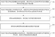
- Embodiment 1 of an FPGA cloud host development method is a flowchart of Embodiment 1 of an FPGA cloud host development method according to an embodiment of the present invention.
- the FPGA cloud host development method provided in this embodiment is used to implement user development of an FPGA in an FPGA cloud host, and the method is developed by the foregoing.
- the user side development device in the system is executed. As shown in FIG. 4, the method includes the following steps:
- the above steps 401-402 are optional steps.
- the template constraint file may also be obtained by other means.
- the user obtains the template constraint file through the FPGA cloud host by logging in to the FPGA cloud host purchased by himself.
- the user obtains the required template constraint file through the interaction between the user development device and the development management platform for designing the design file.
- the user may change the template constraint file, resulting in damage to the FPGA hardware. Therefore, the user's design file needs to be submitted to the development management platform for legality detection.
- the comprehensive report refers to a non-sensitive comprehensive report.
- the user can determine whether to modify the design file by analyzing the comprehensive report. If no modification is needed, the programming instruction for the design file can be triggered to instruct the development management platform to design the design file. The corresponding programming file is programmed into the FPGA.
- the user can remotely develop the FPGA in the FPGA cloud host, which is simple and convenient.
- the foregoing development management platform may be implemented as a server.
- the development management platform may include a processor 11 and a memory 12.
- the memory 12 is configured to store a program that supports the development management platform to execute the FPGA cloud host development method provided in any of the above embodiments, and the processor 11 is configured to execute a program stored in the memory 12.
- the program includes one or more computer instructions, wherein the one or more computer instructions are executed by the processor 11 to implement the following steps:
- the programming file corresponding to the programming instruction is programmed into the FPGA, and the programming file is obtained by the comprehensive processing.
- the processor 11 is further configured to perform all or part of the foregoing method steps.
- the structure of the development management platform may further include a communication interface 13 for the development management platform to communicate with other devices or communication networks, such as communication with user development devices.
- an embodiment of the present invention provides a computer storage medium for storing computer software instructions used in a development management platform, and includes a program involved in executing the FPGA cloud host development method in the foregoing method embodiments.
- the above development device is, for example, a PC, as shown in FIG. 6, the development device may include: a processor 21 and a memory 22.
- the memory 22 is configured to store a program supporting the development device to execute the FPGA cloud host development method provided in any of the above embodiments, and the processor 21 is configured to execute the program stored in the memory 22.
- the program includes one or more computer instructions, wherein the one or more computer instructions are executed by the processor 21 to implement the following steps:
- the programming indication is used to indicate that the programming file corresponding to the design file is programmed into the FPGA.
- the processor 21 is further configured to perform all or part of the foregoing method steps.
- the structure of the development device may further include a communication interface 23 for the development device to communicate with other devices or communication networks, such as communication with the development management platform.
- an embodiment of the present invention provides a computer storage medium for storing computer software instructions for developing a device, which includes a program for executing the FPGA cloud host development method in the foregoing method embodiments.
- the computer program instructions can also be stored in a computer readable memory that can direct a computer or other programmable data processing device to operate in a particular manner, such that the instructions stored in the computer readable memory produce an article of manufacture comprising the instruction device.
- the apparatus implements the functions specified in one or more blocks of a flow or a flow and/or block diagram of the flowchart.
- These computer program instructions can also be loaded onto a computer or other programmable data processing device such that a series of operational steps are performed on a computer or other programmable device to produce computer-implemented processing for execution on a computer or other programmable device.
- the instructions provide steps for implementing the functions specified in one or more of the flow or in a block or blocks of a flow diagram.
- a computing device includes one or more processors (CPUs), input/output interfaces, network interfaces, and memory.
- processors CPUs
- input/output interfaces network interfaces
- memory volatile and non-volatile memory
- the memory may include non-persistent memory, random access memory (RAM), and/or non-volatile memory in a computer readable medium, such as read only memory (ROM) or flash memory.
- RAM random access memory
- ROM read only memory
- Memory is an example of a computer readable medium.
- Computer readable media includes both permanent and non-persistent, removable and non-removable media.
- Information storage can be implemented by any method or technology.
- the information can be computer readable instructions, data structures, modules of programs, or other data.
- Examples of computer storage media include, but are not limited to, phase change memory (PRAM), static random access memory (SRAM), dynamic random access memory (DRAM), other types of random access memory (RAM), read only memory. (ROM), electrically erasable programmable read only memory (EEPROM), flash memory or other memory technology, compact disk read only memory (CD-ROM), digital versatile disk (DVD) or other optical storage, Magnetic tape cartridges, magnetic tape storage or other magnetic storage devices or any other non-transportable media can be used to store information that can be accessed by a computing device.
- computer readable media does not include temporary storage of computer readable media, such as modulated data signals and carrier waves.
Landscapes
- Engineering & Computer Science (AREA)
- Theoretical Computer Science (AREA)
- Software Systems (AREA)
- Physics & Mathematics (AREA)
- Computer Hardware Design (AREA)
- General Engineering & Computer Science (AREA)
- General Physics & Mathematics (AREA)
- Computer Security & Cryptography (AREA)
- Evolutionary Computation (AREA)
- Geometry (AREA)
- Microelectronics & Electronic Packaging (AREA)
- Mathematical Physics (AREA)
- Multimedia (AREA)
- Technology Law (AREA)
- Stored Programmes (AREA)
- Design And Manufacture Of Integrated Circuits (AREA)
Priority Applications (3)
| Application Number | Priority Date | Filing Date | Title |
|---|---|---|---|
| JP2020526207A JP2021502648A (ja) | 2017-11-13 | 2018-11-05 | Fpgaクラウドホストの開発方法およびシステム |
| EP18875358.6A EP3712764B1 (en) | 2017-11-13 | 2018-11-05 | Fpga cloud host development method and system |
| US15/930,113 US11132436B2 (en) | 2017-11-13 | 2020-05-12 | FPGA cloud host development method and system |
Applications Claiming Priority (2)
| Application Number | Priority Date | Filing Date | Title |
|---|---|---|---|
| CN201711117784.6A CN109783118B (zh) | 2017-11-13 | 2017-11-13 | Fpga云主机开发方法和系统 |
| CN201711117784.6 | 2017-11-13 |
Related Child Applications (1)
| Application Number | Title | Priority Date | Filing Date |
|---|---|---|---|
| US15/930,113 Continuation US11132436B2 (en) | 2017-11-13 | 2020-05-12 | FPGA cloud host development method and system |
Publications (1)
| Publication Number | Publication Date |
|---|---|
| WO2019091348A1 true WO2019091348A1 (zh) | 2019-05-16 |
Family
ID=66438210
Family Applications (1)
| Application Number | Title | Priority Date | Filing Date |
|---|---|---|---|
| PCT/CN2018/113901 Ceased WO2019091348A1 (zh) | 2017-11-13 | 2018-11-05 | Fpga云主机开发方法和系统 |
Country Status (5)
| Country | Link |
|---|---|
| US (1) | US11132436B2 (enExample) |
| EP (1) | EP3712764B1 (enExample) |
| JP (1) | JP2021502648A (enExample) |
| CN (1) | CN109783118B (enExample) |
| WO (1) | WO2019091348A1 (enExample) |
Cited By (2)
| Publication number | Priority date | Publication date | Assignee | Title |
|---|---|---|---|---|
| CN111431749A (zh) * | 2020-03-27 | 2020-07-17 | 重庆海云捷迅科技有限公司 | 一种fpga云服务器管理平台及其使用方法 |
| CN111694309A (zh) * | 2020-06-18 | 2020-09-22 | 中国科学技术大学 | 一种fpga线上平台的实现方法 |
Families Citing this family (6)
| Publication number | Priority date | Publication date | Assignee | Title |
|---|---|---|---|---|
| US11128646B1 (en) * | 2018-04-16 | 2021-09-21 | Trend Micro Incorporated | Apparatus and method for cloud-based accelerated filtering and distributed available compute security processing |
| CN110569042B (zh) * | 2019-08-19 | 2022-11-11 | 苏州浪潮智能科技有限公司 | 一种支持虚拟机内更新fpga功能的系统,方法,设备及存储介质 |
| CN114650246B (zh) * | 2020-12-18 | 2025-09-05 | 中国移动通信有限公司研究院 | Ip核调用的检测方法、装置及设备 |
| CN113722271B (zh) * | 2021-07-20 | 2023-11-21 | 湖南艾科诺维科技有限公司 | 用于数据采集回放的文件管理方法、系统及介质 |
| CN114691157B (zh) * | 2022-03-14 | 2025-02-18 | 阿里巴巴(中国)有限公司 | 基于云的fpga管理控制系统、方法及电子设备 |
| CN114611447A (zh) * | 2022-03-16 | 2022-06-10 | 中科亿海微电子科技(苏州)有限公司 | 可编程逻辑器件布线调整方法、装置、计算机及存储介质 |
Citations (4)
| Publication number | Priority date | Publication date | Assignee | Title |
|---|---|---|---|---|
| CN101976431A (zh) * | 2010-11-02 | 2011-02-16 | 公安部第三研究所 | 一种基于动态可重构技术的通用图像处理平台及其实现方法 |
| CN103699399A (zh) * | 2012-09-27 | 2014-04-02 | 中国科学院微电子研究所 | 一种使可部分配置的fpga芯片系统具有高可靠性的方法 |
| US20160321390A1 (en) * | 2015-05-01 | 2016-11-03 | Altera Corporation | Implementing integrated circuit designs using depopulation and repopulation operations |
| CN106155661A (zh) * | 2015-04-14 | 2016-11-23 | 阿里巴巴集团控股有限公司 | 一种控件接入方法及装置 |
Family Cites Families (16)
| Publication number | Priority date | Publication date | Assignee | Title |
|---|---|---|---|---|
| US6711674B1 (en) * | 2000-02-24 | 2004-03-23 | Xilinx, Inc. | Method of watermarking configuration data in an FPGA by embedding the watermark corresponding to a macro obtained upon encountering a first watermark tag from the macro |
| US7073158B2 (en) * | 2002-05-17 | 2006-07-04 | Pixel Velocity, Inc. | Automated system for designing and developing field programmable gate arrays |
| US7802222B2 (en) * | 2006-09-25 | 2010-09-21 | Cadence Design Systems, Inc. | Generalized constraint collection management method |
| US8972958B1 (en) * | 2012-10-23 | 2015-03-03 | Convey Computer | Multistage development workflow for generating a custom instruction set reconfigurable processor |
| CN102156789B (zh) * | 2011-04-27 | 2013-01-02 | 迈普通信技术股份有限公司 | Fpga约束文件自动生成系统及方法 |
| CN103000230B (zh) * | 2011-09-09 | 2016-04-13 | 上海华虹宏力半导体制造有限公司 | 一种非易失性存储器ip核的测试和验证开发系统 |
| CN203416233U (zh) * | 2013-06-24 | 2014-01-29 | 成都鸿芯纪元科技有限公司 | 一种fpga上电复位系统 |
| CN106415583A (zh) | 2014-01-22 | 2017-02-15 | 英派尔科技开发有限公司 | 通过现场可编程门阵列的电压测量结果来检测恶意软件 |
| US9444827B2 (en) | 2014-02-15 | 2016-09-13 | Micron Technology, Inc. | Multi-function, modular system for network security, secure communication, and malware protection |
| RU2015144655A (ru) * | 2015-10-16 | 2017-04-24 | Кейденс Дизайн Системс, Инк. | Процесс проверки достоверности ограничений |
| US10069681B2 (en) * | 2015-12-31 | 2018-09-04 | Amazon Technologies, Inc. | FPGA-enabled compute instances |
| US11017125B2 (en) | 2016-12-13 | 2021-05-25 | University Of Florida Research Foundation, Incorporated | Uniquified FPGA virtualization approach to hardware security |
| US10540506B2 (en) | 2017-01-12 | 2020-01-21 | Microsoft Technology Licensing, Llc | Field-programmable gate array virtualization |
| US10972277B2 (en) | 2017-03-15 | 2021-04-06 | Intel Corporation | Confidential verification of FPGA code |
| US10764129B2 (en) * | 2017-04-18 | 2020-09-01 | Amazon Technologies, Inc. | Logic repository service supporting adaptable host logic |
| CN107273171A (zh) * | 2017-07-10 | 2017-10-20 | 郑州云海信息技术有限公司 | 一种fpga板卡的烧录方法及装置 |
-
2017
- 2017-11-13 CN CN201711117784.6A patent/CN109783118B/zh active Active
-
2018
- 2018-11-05 JP JP2020526207A patent/JP2021502648A/ja active Pending
- 2018-11-05 EP EP18875358.6A patent/EP3712764B1/en active Active
- 2018-11-05 WO PCT/CN2018/113901 patent/WO2019091348A1/zh not_active Ceased
-
2020
- 2020-05-12 US US15/930,113 patent/US11132436B2/en active Active
Patent Citations (4)
| Publication number | Priority date | Publication date | Assignee | Title |
|---|---|---|---|---|
| CN101976431A (zh) * | 2010-11-02 | 2011-02-16 | 公安部第三研究所 | 一种基于动态可重构技术的通用图像处理平台及其实现方法 |
| CN103699399A (zh) * | 2012-09-27 | 2014-04-02 | 中国科学院微电子研究所 | 一种使可部分配置的fpga芯片系统具有高可靠性的方法 |
| CN106155661A (zh) * | 2015-04-14 | 2016-11-23 | 阿里巴巴集团控股有限公司 | 一种控件接入方法及装置 |
| US20160321390A1 (en) * | 2015-05-01 | 2016-11-03 | Altera Corporation | Implementing integrated circuit designs using depopulation and repopulation operations |
Non-Patent Citations (1)
| Title |
|---|
| See also references of EP3712764A4 |
Cited By (3)
| Publication number | Priority date | Publication date | Assignee | Title |
|---|---|---|---|---|
| CN111431749A (zh) * | 2020-03-27 | 2020-07-17 | 重庆海云捷迅科技有限公司 | 一种fpga云服务器管理平台及其使用方法 |
| CN111431749B (zh) * | 2020-03-27 | 2022-10-14 | 重庆海云捷迅科技有限公司 | 一种fpga云服务器管理平台及其使用方法 |
| CN111694309A (zh) * | 2020-06-18 | 2020-09-22 | 中国科学技术大学 | 一种fpga线上平台的实现方法 |
Also Published As
| Publication number | Publication date |
|---|---|
| CN109783118A (zh) | 2019-05-21 |
| US20200272730A1 (en) | 2020-08-27 |
| EP3712764A4 (en) | 2021-08-18 |
| JP2021502648A (ja) | 2021-01-28 |
| CN109783118B (zh) | 2022-10-25 |
| EP3712764B1 (en) | 2024-04-10 |
| US11132436B2 (en) | 2021-09-28 |
| EP3712764A1 (en) | 2020-09-23 |
Similar Documents
| Publication | Publication Date | Title |
|---|---|---|
| WO2019091348A1 (zh) | Fpga云主机开发方法和系统 | |
| US12067126B2 (en) | System and method for application security profiling | |
| US11762763B2 (en) | Orchestration for automated performance testing | |
| US11514172B2 (en) | System and method for information flow analysis of application code | |
| CN106559438B (zh) | 一种基于目标网络平台的程序上传方法和装置 | |
| US10379824B2 (en) | Method for static security enforcement of a DSL | |
| WO2021098148A1 (zh) | 一种软件编译方法、装置及电子设备和存储介质 | |
| US7810072B2 (en) | Exception thrower | |
| WO2022222537A1 (zh) | Ai应用部署方法及相关平台、集群、介质、程序产品 | |
| WO2019072110A1 (zh) | 应用程序的生成方法、装置、系统、设备和介质 | |
| CN101379504B (zh) | 用于复合应用的基于角色的访问控制管理的方法及系统 | |
| CN114116471A (zh) | 一种自动化代码扫描方法、系统、电子设备与存储介质 | |
| CN114879939A (zh) | 生成微服务的方法、系统、电子设备及存储介质 | |
| AU2017276243B2 (en) | System And Method For Generating Service Operation Implementation | |
| CN104318163B (zh) | 一种第三方软件可信构建方法 | |
| CN108595656B (zh) | 一种数据的处理方法及系统 | |
| CN117806688A (zh) | 热更新检测方法、装置、计算机设备和存储介质 | |
| CN114115982A (zh) | 代码发布方法、装置、设备及存储介质 | |
| Hriţcu | Micro-policies: Formally verified, tag-based security monitors | |
| Lincke | Designing software security with UML extensions: post-conference workshop | |
| CN116662136A (zh) | 数据采集方法及其装置 | |
| CN114942746A (zh) | 应用构建发布平台及方法 | |
| Ghorbani | Validation and Verification of Modular Software Applications | |
| CN118626055A (zh) | 项目应用的构建方法、装置、存储介质和电子设备 | |
| JP2024137981A (ja) | ソフトウェア検証方法およびソフトウェア開発システム |
Legal Events
| Date | Code | Title | Description |
|---|---|---|---|
| 121 | Ep: the epo has been informed by wipo that ep was designated in this application |
Ref document number: 18875358 Country of ref document: EP Kind code of ref document: A1 |
|
| ENP | Entry into the national phase |
Ref document number: 2020526207 Country of ref document: JP Kind code of ref document: A |
|
| NENP | Non-entry into the national phase |
Ref country code: DE |
|
| ENP | Entry into the national phase |
Ref document number: 2018875358 Country of ref document: EP Effective date: 20200615 |