WO2019087746A1 - 電源切り替え回路、電源ic及び車載電子制御装置 - Google Patents
電源切り替え回路、電源ic及び車載電子制御装置 Download PDFInfo
- Publication number
- WO2019087746A1 WO2019087746A1 PCT/JP2018/038250 JP2018038250W WO2019087746A1 WO 2019087746 A1 WO2019087746 A1 WO 2019087746A1 JP 2018038250 W JP2018038250 W JP 2018038250W WO 2019087746 A1 WO2019087746 A1 WO 2019087746A1
- Authority
- WO
- WIPO (PCT)
- Prior art keywords
- power supply
- voltage
- switching circuit
- circuit
- diode
- Prior art date
- Legal status (The legal status is an assumption and is not a legal conclusion. Google has not performed a legal analysis and makes no representation as to the accuracy of the status listed.)
- Ceased
Links
Images

Classifications
-
- H—ELECTRICITY
- H02—GENERATION; CONVERSION OR DISTRIBUTION OF ELECTRIC POWER
- H02M—APPARATUS FOR CONVERSION BETWEEN AC AND AC, BETWEEN AC AND DC, OR BETWEEN DC AND DC, AND FOR USE WITH MAINS OR SIMILAR POWER SUPPLY SYSTEMS; CONVERSION OF DC OR AC INPUT POWER INTO SURGE OUTPUT POWER; CONTROL OR REGULATION THEREOF
- H02M1/00—Details of apparatus for conversion
- H02M1/10—Arrangements incorporating converting means for enabling loads to be operated at will from different kinds of power supplies, e.g. from AC or DC
-
- H—ELECTRICITY
- H02—GENERATION; CONVERSION OR DISTRIBUTION OF ELECTRIC POWER
- H02M—APPARATUS FOR CONVERSION BETWEEN AC AND AC, BETWEEN AC AND DC, OR BETWEEN DC AND DC, AND FOR USE WITH MAINS OR SIMILAR POWER SUPPLY SYSTEMS; CONVERSION OF DC OR AC INPUT POWER INTO SURGE OUTPUT POWER; CONTROL OR REGULATION THEREOF
- H02M1/00—Details of apparatus for conversion
- H02M1/0003—Details of control, feedback or regulation circuits
- H02M1/0006—Arrangements for supplying an adequate voltage to the control circuit of converters
-
- H—ELECTRICITY
- H02—GENERATION; CONVERSION OR DISTRIBUTION OF ELECTRIC POWER
- H02M—APPARATUS FOR CONVERSION BETWEEN AC AND AC, BETWEEN AC AND DC, OR BETWEEN DC AND DC, AND FOR USE WITH MAINS OR SIMILAR POWER SUPPLY SYSTEMS; CONVERSION OF DC OR AC INPUT POWER INTO SURGE OUTPUT POWER; CONTROL OR REGULATION THEREOF
- H02M3/00—Conversion of DC power input into DC power output
- H02M3/02—Conversion of DC power input into DC power output without intermediate conversion into AC
- H02M3/04—Conversion of DC power input into DC power output without intermediate conversion into AC by static converters
- H02M3/10—Conversion of DC power input into DC power output without intermediate conversion into AC by static converters using discharge tubes with control electrode or semiconductor devices with control electrode
- H02M3/145—Conversion of DC power input into DC power output without intermediate conversion into AC by static converters using discharge tubes with control electrode or semiconductor devices with control electrode using devices of a triode or transistor type requiring continuous application of a control signal
- H02M3/155—Conversion of DC power input into DC power output without intermediate conversion into AC by static converters using discharge tubes with control electrode or semiconductor devices with control electrode using devices of a triode or transistor type requiring continuous application of a control signal using semiconductor devices only
- H02M3/156—Conversion of DC power input into DC power output without intermediate conversion into AC by static converters using discharge tubes with control electrode or semiconductor devices with control electrode using devices of a triode or transistor type requiring continuous application of a control signal using semiconductor devices only with automatic control of output voltage or current, e.g. switching regulators
- H02M3/158—Conversion of DC power input into DC power output without intermediate conversion into AC by static converters using discharge tubes with control electrode or semiconductor devices with control electrode using devices of a triode or transistor type requiring continuous application of a control signal using semiconductor devices only with automatic control of output voltage or current, e.g. switching regulators including plural semiconductor devices as final control devices for a single load
Definitions
- the present invention relates to a power supply switching circuit, a power supply IC, and an on-vehicle electronic control device.
- a semiconductor integrated circuit IC (Integrated Circuit) mounted on an electronic control device is advanced in function and integration, and power consumption is increased accordingly, and loss and heat generation are increased. If the heat generation of the semiconductor increases, an expensive low thermal resistance package is required to dissipate the heat, or the heat dissipation structure of the substrate or housing on which the semiconductor is mounted or the cost increase of the heat dissipation material may be caused. An issue arises. In order to minimize the cost for these heat dissipation measures, it is required to reduce the power consumption and heat generation of the semiconductor.
- microcomputers microcomputers
- ICs mounted therein are becoming highly functional and highly integrated, and power consumption is also increasing.
- a large power consumption for driving a large current is required for a power supply IC for generating a power supply of a microcomputer and a driver IC for driving an actuator load.
- the power consumption of these ICs can be roughly divided into power consumption by drive current for microcomputer power generation and actuator drive, and power consumption of an internal power supply circuit for driving and signal processing DCDC power supply and driver circuits.
- the power consumption of the internal power supply circuit was small in proportion to the power consumption of the entire IC, so the reduction effect of the power consumption of the internal power supply circuit was small.
- the power consumption and heat generation ratio of the internal power supply circuit are increasing and the influence is increasing as the function and integration of ICs are advanced.
- the on-vehicle electronic control device there is a battery as a main power source to be supplied, and this battery voltage is directly or step down and boosted to generate a desired voltage required for control.
- this battery voltage is directly or step down and boosted to generate a desired voltage required for control.
- it is generally considered to lower the applied voltage or the consumed current, and if the current consumption is constant, the power consumption can be reduced by lowering the driving voltage. It becomes possible.
- the function of the internal power supply circuit of the power supply IC is a reference voltage in the IC, generation of a reference clock, DCDC power supplies, driving of each driver circuit, communication function with a microcomputer, and the like. Therefore, when the internal circuit is driven with a voltage stepped down from the battery voltage by the DCDC power supply, the internal power supply circuit is first driven by the battery. After that, it is necessary to supply a voltage stepped down by the DCDC power supply to the internal power supply circuit, and a circuit to switch the battery voltage and the stepped-down voltage is needed.
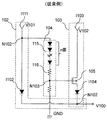
- FIG. 7 is a block diagram of the power supply switching circuit described in Patent Document 1. As shown in FIG. When applied to a FlexRay transceiver IC, V102 corresponds to the battery voltage VBAT, and V101 corresponds to the VCC power supply voltage. When the VCC power supply voltage is lower than a predetermined voltage, power is supplied from V 102 by activating the PMOS 105.
- the power supply circuit of FIG. 7 realizes a power supply switching circuit that operates properly, with no current other than the current flowing through the transceiver IC flowing even in the low power consumption mode.
- the output voltage of the switching circuit described in Patent Document 1 described above is a voltage obtained by reducing the forward voltage of each of the diodes from V101 and V102. That is, this output voltage depends on the voltages of V101 and V102, and when the voltage difference is large, the output voltage to be switched also largely fluctuates.
- the internal power supply circuit of the integrated circuit needs to constantly generate a reference voltage and a reference clock stably. However, if switching causes a large voltage fluctuation or a momentary voltage drop, the reference voltage or reference clock fluctuation, or the output of the internal power supply circuit decreases, which causes a problem in stable operation at switching. There is.
- the object of the present invention is to switch the first power supply and the second power supply according to the voltage of the second power supply and to output a voltage independent of the voltage of the first power supply using the first power supply, etc. To provide.
- the present invention is connected to a first node connecting a current path connected to a first power supply and a current path connected to a second power supply supplying a voltage lower than the first power supply.
- Output terminal a resistor connected to the first power supply, a Zener diode connected in series to the resistor, and a control electrode connected to a second node connecting the resistor and the Zener diode.
- FIG. 6 is a circuit diagram showing a configuration of a power supply switching circuit described in Patent Document 1.
- An object of the present embodiment is to continuously operate the internal power supply circuit stably at the time of switching the power supply and to reduce the power consumption of the internal power supply circuit by switching the power supply.
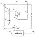
- FIG. 1 is a circuit diagram of a power supply switching circuit 12 according to a first embodiment of the present invention.
- the power supply switching circuit 12 of FIG. 1 includes a Zener diode 22, a resistor 20, an NMOS 23 (N-channel Metal Oxide Semiconductor), and a second diode 24.
- the output terminal OUT is connected to a first node 26 connecting a current path connected to the first power supply V1 and a current path connected to the second power supply V2 supplying a voltage lower than that of the first power supply V1.
- Ru The resistor 20 is connected to the first power supply V1.
- the zener diode 22 is connected in series to the resistor 20.
- the NMOS 23 transistor
- the NMOS 23 has a gate (control electrode) connected to the second node 27 connecting the resistor 20 and the Zener diode 22, and according to the voltage applied to the gate, the first power supply V1 and the output terminal Turn on / off the current path between OUT.
- the second diode 24 rectifies the current flowing in the current path between the second power supply V2 and the output terminal OUT.
- the rise of the voltage of the second node 27 activates the NMOS 23, and the first node 26 is biased in accordance with the voltage between the gate and the source of the NMOS 23. Thus, the voltage is output to the first node 26 by the supply of the first power supply V1. At this time, the second diode 24 has a backflow prevention function.
- the voltage V3 is a voltage for driving the internal power supply circuit 13, and has to be higher than the output voltage of the internal power supply circuit 13. By the supply of the voltage V3, the internal power supply circuit 13 generates an output voltage V4.
- the first node voltage V3B becomes a voltage V2-Vf2 and is supplied from the second power supply V2, and the power supply of V3 is switched from the first power supply V1 to the second power supply V2.
- the voltage V3A0 In order to switch to the second power supply V2, the voltage V3A0 needs to be set lower than the voltage V2-Vf2.
- the power consumption of the internal power supply circuit 13 is current I3
- the power consumption is switched from V1 ⁇ I3 at the time of supplying the first power supply V1 to V2 ⁇ I3 at the time of supplying the second power supply V2, and the second power supply V2 is By lowering it, the power consumption of the internal power supply circuit and the heat generation associated therewith can be reduced.
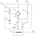
- FIG. 2 is a circuit diagram of a power supply switching circuit 12A according to a first modification of the first embodiment of the present invention.
- the power supply switching circuit 12 shown in FIG. 1 has a configuration in which a second capacitor 25 disposed between the first node 26 and the internal power supply circuit 13 is added. That is, one end of the second capacitor 25 is connected to the output terminal OUT.
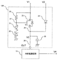
- FIG. 3 is a circuit diagram of a power supply switching circuit 12B according to a second modification of the first embodiment of the present invention.
- the configuration is such that the first diode 21 disposed between the second node 27 and the Zener diode 22 is added to the power supply switching circuit 12A shown in FIG. That is, the first diode 21 has an anode connected to the second node 27 and a cathode connected to the cathode of the zener diode 22.
- the first diode 21 cancels the negative temperature characteristic of the voltage of the NMOS 23 (transistor).
- the power supply switching circuit 12B of FIG. 3 includes a Zener diode 22, a first diode 21, a resistor 20, an NMOS 23, a second diode 24, and a second capacitor 25.
- the rise of the voltage of the second node 27 activates the NMOS 23, and the first node 26 is biased in accordance with the voltage between the gate and the source of the NMOS 23. Thus, the voltage is output to the first node 26 by the supply of the first power supply V1. At this time, the second diode 24 has a backflow prevention function.
- the output terminal voltage V3 of the first node 26 is substantially independent of the first power supply V1, and is constant determined by the voltage Vz of the Zener diode 22, the voltage Vf1 of the first diode 21, the gate-to-source voltage Vgs of the NMOS 23.
- the voltage V3A Vz + Vf1-Vgs.
- the output terminal OUT is a constant voltage independent of the voltage of the first power supply V1.
- V3A Vz + Vf1-Vgs (first voltage) is output from the first power supply V1 through the NMOS 23 (transistor).
- the gate and source voltages of the NMOS 23 also have negative temperature characteristics, so that the temperature dependency is canceled out.
- the voltage V3 can be output to the first node 26 with low temperature dependency by using the Zener diode 22 with low temperature dependency.
- the voltage V3 is a voltage for driving the internal power supply circuit 13, and has to be higher than the output voltage of the internal power supply circuit 13. By the supply of the voltage V3, the internal power supply circuit 13 generates an output voltage V4.
- the first node voltage V3B becomes a voltage V2-Vf2 and is supplied from the second power supply V2, and the power supply of V3 is switched from the first power supply V1 to the second power supply V2.
- the output terminal OUT outputs the second voltage (V2-Vf2) from the second power supply V2 through the second diode 24 when the voltage of the second power supply V2 is higher than the predetermined voltage (Vz + Vf1-Vgs + Vf2).
- the voltage V3A In order to switch to the second power supply V2, the voltage V3A needs to be set lower than the voltage V2-Vf2.
- the power consumption of the internal power supply circuit 13 is current I3
- the power consumption is switched from V1 ⁇ I3 at the time of supplying the first power supply V1 to V2 ⁇ I3 at the time of supplying the second power supply V2, and the second power supply V2 is By lowering it, the power consumption of the internal power supply circuit and the heat generation associated therewith can be reduced.
- the power supply switching circuit according to the first embodiment of the present invention can switch the output voltage V3 from the first power supply V1 to the second power supply V2 when the voltage V2 becomes equal to or higher than a desired voltage.
- the V2 voltage can be set to a voltage lower than the V1 voltage, it is possible to reduce the power consumption and heat generation of the internal power supply circuit 13 connected to V3.
- the first power supply can be used to output a voltage independent of the voltage of the first power supply.
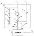
- FIG. 4 is a circuit diagram of a power supply switching circuit 12C according to a second embodiment of the present invention.
- a third diode 29 disposed between the first node 26 and the NMOS 23 is added. That is, the third diode 29 has an anode connected to the source of the NMOS 23 (transistor) and a cathode connected to the first node 26.
- the voltage V2 becomes higher than the voltage V1
- the V2 voltage for switching the power supply is a voltage which is V2 ⁇ Vf2> Vz + Vf1 ⁇ Vgs ⁇ Vf3.
- the power supply switching circuit switches the output voltage V3 from the first power supply V1 to the second power supply V2 when the V2 voltage is equal to or higher than the desired voltage, as in the first embodiment. I can do it.
- the V2 voltage is set to a voltage lower than the V1 voltage, it is possible to reduce the power consumption and heat generation of the internal power supply circuit 13 connected to V3.
- the V2 voltage is higher than the V1 voltage, it is possible to prevent the current from flowing back to the first power supply V1.
- FIG. 5 is a block diagram of an on-vehicle electronic control device 31 provided with a power supply IC 11 according to a third embodiment of the present invention.
- the power supply IC 11 incorporates the power supply switching circuit 12 (or 12A to 12C), the internal power supply circuit 13, the step-down switching regulator 14, the series power supply 15, and the driver circuit 16.
- the battery 10 is connected to the first power supply V1 of the power supply switching circuit 12, and the output voltage V5 obtained by smoothing the switching output of the step-down switching regulator 14 with the inductor 17 and the first capacitor 18 is used for the second power supply V2.
- the first power source V1 is the battery 10 (battery power source)
- the second power source V2 is the step-down switching regulator 14.
- the internal power supply circuit 13 is connected to the output terminal voltage V3.
- the output voltage V4 of the internal power supply circuit 13 is connected to the step-down switching regulator 14, each series power supply 15, and the driver circuit 16, and becomes a power supply voltage for driving each circuit.
- the step-down switching regulator 14 is connected to the battery 10 and steps down from the battery 10 to generate a voltage V5 required for the series power supply 15.
- the voltage V5 is a negative feedback voltage of the step-down switching regulator 14.
- the series power supply 15 generates a plurality of power supply voltages V6 and V7 required for the microcomputer 30 and power supply voltages V8 for various sensors 34 for detecting information required for vehicle control, by stepping down from the V5 voltage.
- the driver circuit 16 also drives a plurality of actuator loads 32 and 33 mounted on the vehicle.
- the power supply switching circuit 12 raises the V2 voltage lower than the V1 voltage to a desired voltage or higher, whereby the V5 voltage is connected to the internal power supply circuit 13.
- the power consumption P1 of the internal power supply circuit 13 driven with a lower V2 voltage is reduced to V5 ⁇ I3.
- the current I3 of the internal power supply circuit 13 is newly supplied via V5, so the power consumption of the step-down switching regulator 14 is increased.
- the efficiency of the step-down switching regulator 14 is K and the power consumption P1 of the internal power supply circuit 13
- the battery 10 voltage is 14 V
- the V5 voltage is 6 V
- the conversion efficiency is 90%
- the power supply IC 11 generates a plurality of power supplies for driving the microcomputer 30, and it is necessary to terminate the internal power supply circuit 13 after the plurality of power supplies have ended normally.
- the internal power supply circuit 13 is stably driven from the voltage V0 by the operation of the power supply switching circuit 12, whereby the power supply IC11 is assured. It is possible to complete the termination sequence.
- the internal power supply circuit 13 is stably driven from the V0 voltage by the operation of the power supply switching circuit 12.
- the internal power supply circuit 13 is driven by the voltage V5, and power consumption is similarly reduced.
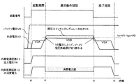
- FIG. 6 is a time chart of the power supply IC according to the third embodiment.
- t0 indicates the timing when the start signal is input.
- the period from t0 to t1 is a startup period in which the internal power supply circuit 13, the step-down switching regulator 14 and each series power supply 15 mounted on the power supply IC 11 are activated.
- the internal voltage V3A Vz + Vf1-Vgs of the power supply switching circuit 12 is supplied from the battery voltage V0.
- the internal power supply circuit 13 starts the V4 voltage.
- the step-down switching regulator 14 is activated and the output voltage V5 rises.
- the power supply switching circuit 12 operates to supply power from V5 to the internal power supply circuit 13, and the power consumption of the power supply IC11 is reduced.
- step-down switching regulator 14 is activated by voltage V4 (third voltage) supplied from internal power supply circuit 13. After that, the step-down switching regulator 14 supplies the output voltage V5 to the internal power supply circuit 13.
- T1 to t2 indicate the normal operation period of the power supply IC 11.
- the on-vehicle electronic control device including the microcomputer continues the normal operation, and the power consumption of the power supply IC 11 becomes the largest.
- the voltage V5 is constantly output, and the power consumption of the internal power supply circuit 13 is reduced to about half, so that the power consumption of the power supply IC 11 is suppressed and the heat generation is also reduced.
- T2 to t3 indicate the end period of the power supply IC 11.
- the fall of the start signal shuts off the step-down switching regulator 14 and each series power supply 15, and finally, a termination sequence in which the internal power supply circuit is turned off is started.
- the internal power supply circuit 13 switches to the drive from the battery power supply V0 by the operation of the power supply switching circuit 12 and continues the stable operation. It becomes possible. That is, when the voltage supplied from the step-down switching regulator 14 to the internal power supply circuit 13 is lower than the predetermined voltage (Vz + Vf1-Vgs + Vf2) in the end sequence, the power supply switching circuit 12 sets V3A (first voltage) to the battery 10 (battery power). ) Through the NMOS 23 (transistor).
- the power supply IC 11 operates in the end period and the operation of the on-vehicle control device by the microcomputer is stopped. There is no influence on heat generation etc.
- the power consumption of the internal power supply circuit 13 is not reduced, but the power consumption of the entire power supply IC is sufficiently small so that there is no influence on heat generation.
- the internal power supply circuit 13 supplies the output voltage V4 to the step-down switching regulator 14.
- the present invention is not limited to the above-described embodiment, but includes various modifications.
- the embodiments described above are described in detail in order to explain the present invention in an easy-to-understand manner, and are not necessarily limited to those having all the described configurations.
- part of the configuration of one embodiment can be replaced with the configuration of another embodiment, and the configuration of another embodiment can be added to the configuration of one embodiment.
- step-down switching regulator 14 is provided inside the power supply IC 11 in the above embodiment, it may be provided outside the power supply IC 11.
- NMOS 23 is used as the transistor in the above embodiment, an NPN bipolar transistor may be used.
- the embodiment of the present invention may have the following aspects.
- a diode for temperature characteristic correction, a zener diode for generating a reference voltage, and a reference voltage generated by the zener voltage and the forward voltage of the diode is connected to the gate of the NMOS transistor.
- An on-vehicle electronic control device including the power supply switching circuit according to any one of (1) to (5), wherein the power supply switching circuit is mounted on a power supply IC.
- the internal voltage is driven using a battery voltage at the time of start-up, and the step-down switching regulator is activated after the step-down switching regulator is activated.
- a power supply IC for applying the voltage of (1) to the internal power supply.
- the power supply to the internal power supply circuit can be stably switched with small voltage fluctuation.
- the power consumption of the internal power supply circuit can be reduced and the heat generation of the IC can be reduced by switching between the battery voltage and the step-down switching regulator output voltage.
- it is possible to select a low cost package with relatively large thermal resistance by reducing the heat generation of the IC simplify the heat dissipation structure of the chassis of the on-vehicle control device to finally dissipate the heat generation of the IC, and reduce the cost of heat dissipation material. And the cost reduction of the on-vehicle control device.
Landscapes
- Engineering & Computer Science (AREA)
- Power Engineering (AREA)
- Direct Current Feeding And Distribution (AREA)
- Dc-Dc Converters (AREA)
Abstract
第2電源の電圧に応じて第1電源と第2電源を切り替えつつ、第1電源を用いて第1電源の電圧に依存しない電圧を出力することができる電源切り替え回路等を提供する。 出力端子OUTは、第1電源V1に接続される電流経路と第1電源V1より低い電圧を供給する第2電源V2に接続される電流経路とを接続する第1ノード26に接続される。抵抗20は、第1電源V1に接続される。ツェナーダイオード22は、抵抗20に直列に接続される。NMOS23(トランジスタ)は、抵抗20とツェナーダイオード22とを接続する第2ノード27に接続されるゲート(制御電極)を有し、ゲートに印加される電圧に応じて、第1電源V1と出力端子OUTの間の電流経路をオン/オフする。第2ダイオード24は、第2電源V2と出力端子OUTの間の電流経路を流れる電流を整流する。
Description
本発明は、電源切り替え回路、電源IC及び車載電子制御装置に関する。
電子制御装置に搭載される半導体集積回路IC(Integrated Circuit)は高機能化、高集積化が進んでおり、それに伴い消費電力が増大し、損失、発熱が増大している。半導体の発熱が増大すると、その熱を放熱するために高価な低熱抵抗のパッケージが必要となったり、また半導体が実装される基板や筐体の放熱構造や放熱材料の高コスト化を招いたりという課題が発生する。これら放熱対策のためのコストを最小限にするため、半導体の消費電力、発熱の低減が求められている。
車載電子制御装置においても、搭載されるマイクロコンピュータ(マイコン)やICなどの半導体は高機能化、高集積化が進んでおり消費電力も増大している。その中で、マイコンの電源を生成する電源ICやアクチュエータ負荷を駆動するためのドライバICには、大電流駆動のための大きな消費電力が求められる。
これらICの消費電力は、マイコンの電源生成やアクチュエータ駆動のための駆動電流による消費電力と、DCDC電源やドライバ回路を駆動、信号処理するための内部電源回路の消費電力に大別できる。
従来この内部電源回路の消費電力は、IC全体の消費電力に対して割合が小さかったため、内部電源回路の消費電力の削減効果は小さかった。しかし、ICの高機能化、高集積化が進むにつれて、この内部電源回路の消費電力、発熱の割合は増加し、影響が大きくなっている。
車載電子制御装置では、供給される主な電源としてバッテリがあり、このバッテリ電圧を直接、もしくは降圧、昇圧して制御に必要な所望の電圧を生成している。内部電源回路の消費電力を下げるためには、一般的に印加される電圧か消費する電流を下げることが考えられ、消費電流を一定とすると駆動する電圧を下げることで、消費電力を下げることが可能となる。
ここで、電源ICの内部電源回路の機能は、IC内部の基準電圧、基準クロックの生成、各DCDC電源、各ドライバ回路の駆動、マイコンとの通信機能等である。そのため、バッテリ電圧からDCDC電源によって降圧した電圧で内部回路を駆動する場合は、まずはバッテリで内部電源回路を駆動する。その後、DCDC電源によって降圧した電圧を内部電源回路に供給する必要があり、バッテリ電圧と降圧した電圧を切り替える回路が必要となる。
半導体集積回路において、複数の電圧を選択するための電源切り替え技術が知られている。例えば、特許文献1に記載の技術は、Flex Ray規格のトランシーバICに適用した場合、低消費電力モードであっても余剰な回路電流を必要とせず適切に動作することが出来る。
図7は、特許文献1に記載の電源切り替え回路の構成図である。Flex Ray規格のトランシーバICに適用した場合、V102がバッテリ電圧VBAT、V101がVCC電源電圧に相当する。VCC電源電圧が所定の電圧よりも低いときはPMOS105を活性化することにより、V102から電源が供給される。
図7の電源回路は、PMOS105を活性化させることにより、低消費電力モードであってもトランシーバICに流れる電流以外の電流は流れず、適切に動作する電源切り替え回路を実現している。
電子制御装置に搭載される半導体集積回路の内部電源回路で発生する消費電力、またそれに伴う発熱を低減するため、内部電源回路に接続される電圧をより低電圧で駆動するように切り替える必要がある。
上述の特許文献1に記載された切り替え回路の出力電圧は、V101とV102からそれぞれダイオードの順方向電圧だけ低下した電圧となる。すなわち、この出力電圧は、V101とV102の電圧に依存し、その電圧差が大きいと切り替わる出力電圧も大きく変動することになる。
特許文献1に記載された切り替え回路を半導体集積回路の内部電源回路への接続に適用し、バッテリ電圧とDCDC電源電圧とを切り替えて駆動すると、切り替わる出力電圧がバッテリ電圧とDCDC電源電圧に依存して大きく変動してしまう。
また、V101が急に電源低下した場合は、抵抗列116やPMOS105のゲート容量などで発生する時定数により、PMOS105の活性化が遅れ、切り替わりの瞬間に出力電圧の低下が発生することが考えられる。
集積回路の内部電源回路は、基準電圧や基準クロックを常時安定して生成する必要がある。しかし、切り替わりにより、電圧が大きく変動したり、瞬間的な電圧の低下が発生したりすると、基準電圧や基準クロックの変動、または内部電源回路出力が低下するなど、切り替り時の安定動作に課題がある。
本発明の目的は、第2電源の電圧に応じて第1電源と第2電源を切り替えつつ、第1電源を用いて第1電源の電圧に依存しない電圧を出力することができる電源切り替え回路等を提供することにある。
上記目的を達成するために、本発明は、第1電源に接続される電流経路と前記第1電源より低い電圧を供給する第2電源に接続される電流経路とを接続する第1ノードに接続される出力端子と、前記第1電源に接続される抵抗と、前記抵抗に直列に接続されるツェナーダイオードと、前記抵抗と前記ツェナーダイオードとを接続する第2ノードに接続される制御電極を有し、前記制御電極に印加される電圧に応じて、前記第1電源と前記出力端子の間の電流経路をオン/オフするトランジスタと、前記第2電源と前記出力端子の間の電流経路を流れる電流を整流する第2ダイオードと、を備える。
本発明によれば、第2電源の電圧に応じて第1電源と第2電源を切り替えつつ、第1電源を用いて第1電源の電圧に依存しない電圧を出力することができる。上記した以外の課題、構成及び効果は、以下の実施形態の説明により明らかにされる。
以下、添付図面を参照して、本発明の実施形態1~3に係る電源切り替え回路、電源IC、及び車載電子制御装置の構成を詳細に説明する。なお、各図において、同一符号は同一部分を示す。本実施形態では、電源の切り替え時に、内部電源回路を継続して安定動作させ、電源の切り替えにより内部電源回路の消費電力を低減することを目的とする。
(実施形態1)
図1は、本発明の実施形態1に係る電源切り替え回路12の回路図である。
図1は、本発明の実施形態1に係る電源切り替え回路12の回路図である。
図1の電源切り替え回路12は、ツェナーダイオード22、抵抗20、NMOS23(N-channel Metal Oxide Semiconductor)、および第2ダイオード24で構成される。
ここで、出力端子OUTは、第1電源V1に接続される電流経路と第1電源V1より低い電圧を供給する第2電源V2に接続される電流経路とを接続する第1ノード26に接続される。抵抗20は、第1電源V1に接続される。ツェナーダイオード22は、抵抗20に直列に接続される。NMOS23(トランジスタ)は、抵抗20とツェナーダイオード22とを接続する第2ノード27に接続されるゲート(制御電極)を有し、ゲートに印加される電圧に応じて、第1電源V1と出力端子OUTの間の電流経路をオン/オフする。第2ダイオード24は、第2電源V2と出力端子OUTの間の電流経路を流れる電流を整流する。
まず、第1電源V1が供給されると、抵抗20を介して、ツェナーダイオード22に電流が供給され、第2ノード27の電圧は、ツェナーダイオード22の電圧と第2ダイオードの電圧とでバイアスされる。
第2ノード27の電圧の上昇によって、NMOS23が活性化し、NMOS23のゲート、ソース間電圧に応じて第1ノード26がバイアスされる。このように、第1電源V1の供給により、第1ノード26に電圧が出力される。このとき、第2ダイオード24は逆流防止の機能となっている。
ここで、第1ノード26の出力端子電圧V3は、第1電源V1にほとんど依存せず、ツェナーダイオード22の電圧Vz、NMOS23のゲート、ソース間電圧Vgsで決まる一定電圧V3A0=Vz-Vgsとなる。
この電圧V3は、内部電源回路13を駆動するための電圧であり、内部電源回路13の出力電圧よりも高い電圧である必要がある。電圧V3の供給により、内部電源回路13は出力電圧V4を生成する。
ここで、第2電源V2が供給された場合、第2電源V2が第1電源V1から供給された電圧V3A0=Vz-Vgsよりさらに第2ダイオード24の電圧Vf2以上となったとき、第2電源V2から第1ノード26へ電流が流れる。
そのとき、第1ノード電圧V3Bは、V2-Vf2電圧となり第2電源V2から供給され、V3の供給電源が第1電源V1から第2電源V2に切り替る。
第2電源V2への切り替りのため、V3A0の電圧は、V2-Vf2電圧よりも低く設定する必要がある。
内部電源回路13の消費電流を電流I3とすると、この電源切り替わりにより、消費電力は、第1電源V1供給時のV1×I3から第2電源V2供給時のV2×I3となり、第2電源V2を下げることで内部電源回路の消費電力、およびそれに伴う発熱を低減することが出来る。
次に、第2電源V2が低下したときは、V1からV2への切り替りと同様に、V2-Vf2電圧がV3A0電圧よりも低くなったとき、NMOS23のゲート、ソース間電圧Vgsが十分に開くことで、NMOS23が活性化し、第1電源V1から電流が供給され電源電圧が切り替る。
(変形例1)
図2は、本発明の実施形態1の変形例1に係る電源切り替え回路12Aの回路図である。図1に示す電源切り替え回路12に、第1ノード26と内部電源回路13の間に配置される第2コンデンサ25を追加した構成である。すなわち、出力端子OUTに第2コンデンサ25の一端が接続される。
図2は、本発明の実施形態1の変形例1に係る電源切り替え回路12Aの回路図である。図1に示す電源切り替え回路12に、第1ノード26と内部電源回路13の間に配置される第2コンデンサ25を追加した構成である。すなわち、出力端子OUTに第2コンデンサ25の一端が接続される。
V2からV1への切り替り時、V2が急峻に低下した場合を考慮すると、NMOS23からの電流供給が遅くなり、瞬間的にV3の電圧が低下することが考えられる。そのため、第2コンデンサ25を接続し、急峻な切り替り時は第2コンデンサ25から電流を供給することで、内部電源回路の安定動作が維持される。
(変形例2)
図3は、本発明の実施形態1の変形例2に係る電源切り替え回路12Bの回路図である。図2に示す電源切り替え回路12Aに、第2ノード27とツェナーダイオード22の間に配置される第1ダイオード21を追加した構成である。すなわち、第1ダイオード21は、第2ノード27に接続されるアノード、及びツェナーダイオード22のカソードに接続されるカソードを有する。第1ダイオード21によりNMOS23(トランジスタ)の電圧の負の温度特性がキャンセルされる。
図3は、本発明の実施形態1の変形例2に係る電源切り替え回路12Bの回路図である。図2に示す電源切り替え回路12Aに、第2ノード27とツェナーダイオード22の間に配置される第1ダイオード21を追加した構成である。すなわち、第1ダイオード21は、第2ノード27に接続されるアノード、及びツェナーダイオード22のカソードに接続されるカソードを有する。第1ダイオード21によりNMOS23(トランジスタ)の電圧の負の温度特性がキャンセルされる。
詳細には、図3の電源切り替え回路12Bは、ツェナーダイオード22、第1ダイオード21、抵抗20、NMOS23、第2ダイオード24、および第2コンデンサ25で構成される。
まず、第1電源V1が供給されると、抵抗20を介して、第1ダイオード21、ツェナーダイオード22に電流が供給され、第2ノード27の電圧は、ツェナーダイオード22の電圧と第2ダイオードの電圧とでバイアスされる。
第2ノード27の電圧の上昇によって、NMOS23が活性化し、NMOS23のゲート、ソース間電圧に応じて第1ノード26がバイアスされる。このように、第1電源V1の供給により、第1ノード26に電圧が出力される。このとき、第2ダイオード24は逆流防止の機能となっている。
ここで、第1ノード26の出力端子電圧V3は、第1電源V1にほとんど依存せず、ツェナーダイオード22の電圧Vz、第1ダイオード21の電圧Vf1、NMOS23のゲート、ソース間電圧Vgsで決まる一定電圧V3A=Vz+Vf1-Vgsとなる。
すなわち、ツェナーダイオード22と第1ダイオード21によって生成される基準電圧がNMOS23(トランジスタ)のゲート(制御電極)に印加されることにより、出力端子OUTは、第1電源V1の電圧に依存しない一定電圧V3A=Vz+Vf1-Vgs(第1電圧)を第1電源V1からNMOS23(トランジスタ)を介して出力する。
温度特性についても、第1ダイオード21が負の温度特性を持つが、NMOS23のゲート、ソース電圧も負の温度特性であるため温度依存性を打ち消し合う。温度依存性の小さいツェナーダイオード22を使用することで、温度依存性の小さい第1ノード26に電圧V3を出力することが出来る。
この電圧V3は、内部電源回路13を駆動するための電圧であり、内部電源回路13の出力電圧よりも高い電圧である必要がある。電圧V3の供給により、内部電源回路13は出力電圧V4を生成する。
ここで、第2電源V2が供給された場合、第2電源V2が第1電源V1から供給された電圧V3A=Vz+Vf1-Vgsよりさらに第2ダイオード24の電圧Vf2以上となったとき、第2電源V2から第1ノード26へ電流が流れる。
そのとき、第1ノード電圧V3Bは、V2-Vf2電圧となり第2電源V2から供給され、V3の供給電源が第1電源V1から第2電源V2に切り替る。
すなわち、出力端子OUTは、第2電源V2の電圧が所定電圧(Vz+Vf1-Vgs+Vf2)より高い場合、第2電圧(V2-Vf2)を第2電源V2から第2ダイオード24を介して出力する。
第2電源V2への切り替りのため、V3Aの電圧は、V2-Vf2電圧よりも低く設定する必要がある。
内部電源回路13の消費電流を電流I3とすると、この電源切り替わりにより、消費電力は、第1電源V1供給時のV1×I3から第2電源V2供給時のV2×I3となり、第2電源V2を下げることで内部電源回路の消費電力、およびそれに伴う発熱を低減することが出来る。
次に、第2電源V2が低下したときは、V1からV2への切り替りと同様に、V2-Vf2電圧がV3A電圧よりも低くなったとき、NMOS23のゲート、ソース間電圧Vgsが十分に開くことで、NMOS23が活性化し、第1電源V1から電流が供給され電源電圧が切り替る。
すなわち、出力端子OUTは、第2電源V2の電圧が所定電圧(Vz+Vf1-Vgs+Vf2)より低い場合、一定電圧V3A=Vz+Vf1-Vgs(第1電圧)を第1電源V1からNMOS23(トランジスタ)を介して出力する。
(実施形態1のまとめ)
以上のように、本発明の実施形態1に係る電源切り替え回路は、V2電圧が所望の電圧以上となると、出力電圧V3を第1電源V1から第2電源V2に切り替えることが出来る。これにより、V2電圧をV1電圧より低電圧と設定することで、V3に接続される内部電源回路13の消費電力、発熱を低減することが出来る。また、第2電源の電圧に応じて第1電源と第2電源を切り替えつつ、第1電源を用いて第1電源の電圧に依存しない電圧を出力することができる。
以上のように、本発明の実施形態1に係る電源切り替え回路は、V2電圧が所望の電圧以上となると、出力電圧V3を第1電源V1から第2電源V2に切り替えることが出来る。これにより、V2電圧をV1電圧より低電圧と設定することで、V3に接続される内部電源回路13の消費電力、発熱を低減することが出来る。また、第2電源の電圧に応じて第1電源と第2電源を切り替えつつ、第1電源を用いて第1電源の電圧に依存しない電圧を出力することができる。
(実施形態2)
図4は、本発明の実施形態2に係る電源切り替え回路12Cの回路図である。電源切り替え回路12に、第1ノード26とNMOS23の間に配置される第3ダイオード29を追加した構成である。すなわち、第3ダイオード29は、NMOS23(トランジスタ)のソースに接続されるアノード、及び第1ノード26に接続されるカソードを有する。これにより、V2電圧がV1電圧よりも高くなっても、第1電源V1への電流の逆流を防ぐことが出来る。
図4は、本発明の実施形態2に係る電源切り替え回路12Cの回路図である。電源切り替え回路12に、第1ノード26とNMOS23の間に配置される第3ダイオード29を追加した構成である。すなわち、第3ダイオード29は、NMOS23(トランジスタ)のソースに接続されるアノード、及び第1ノード26に接続されるカソードを有する。これにより、V2電圧がV1電圧よりも高くなっても、第1電源V1への電流の逆流を防ぐことが出来る。
しかし、実施形態1の構成と比較して、低電圧での下限の動作電圧範囲が第3ダイオードの順方向電圧のVf3だけ高くなるという点がある。
電源が切り替るためのV2電圧は、V2-Vf2>Vz+Vf1-Vgs-Vf3となる電圧である。
(実施形態2のまとめ)
以上のように、本発明の実施形態2に係る電源切り替え回路は、実施形態1と同様に、V2電圧が所望の電圧以上となると、出力電圧V3を第1電源V1から第2電源V2に切り替えることが出来る。これにより、V2電圧をV1電圧より低電圧と設定することで、V3に接続される内部電源回路13の消費電力、発熱を低減することが出来る。また、V2電圧がV1電圧よりも高くなる場合があっても、第1電源V1への電流が逆流することを防止できる。
以上のように、本発明の実施形態2に係る電源切り替え回路は、実施形態1と同様に、V2電圧が所望の電圧以上となると、出力電圧V3を第1電源V1から第2電源V2に切り替えることが出来る。これにより、V2電圧をV1電圧より低電圧と設定することで、V3に接続される内部電源回路13の消費電力、発熱を低減することが出来る。また、V2電圧がV1電圧よりも高くなる場合があっても、第1電源V1への電流が逆流することを防止できる。
(実施形態3)
図5は、本発明の実施形態3に係る電源IC11を備えた車載電子制御装置31の構成図である。電源IC11は、電源切り替え回路12(又は12A~12C)、内部電源回路13、降圧スイッチングレギュレータ14、シリーズ電源15、ドライバ回路16を内蔵する。
図5は、本発明の実施形態3に係る電源IC11を備えた車載電子制御装置31の構成図である。電源IC11は、電源切り替え回路12(又は12A~12C)、内部電源回路13、降圧スイッチングレギュレータ14、シリーズ電源15、ドライバ回路16を内蔵する。
この電源IC11では、電源切り替え回路12の第1電源V1にはバッテリ10が接続され、第2電源V2には降圧スイッチングレギュレータ14のスイッチング出力をインダクタ17と第1コンデンサ18で平滑した出力電圧V5が接続される。すなわち、第1電源V1は、バッテリ10(バッテリ電源)であり、第2電源V2は、降圧スイッチングレギュレータ14である。また、出力端子電圧V3には内部電源回路13が接続される。
内部電源回路13の出力電圧V4は、降圧スイッチングレギュレータ14、各シリーズ電源15、ドライバ回路16に接続され、各回路を駆動するための電源電圧となる。降圧スイッチングレギュレータ14は、バッテリ10に接続され、バッテリ10から降圧してシリーズ電源15に必要な電圧V5を生成する。また電圧V5は降圧スイッチングレギュレータ14の負帰還電圧となっている。
次にシリーズ電源15により、マイコン30に必要な複数の電源電圧V6、V7や車両制御に必要な情報を検出するための各種センサ34用の電源電圧V8がV5電圧から降圧されて生成される。また、ドライバ回路16により、車両に搭載された複数のアクチュエータ負荷32、33が駆動される。
まず、内部電源回路13に流れるV3の消費電流をI3とすると、電源切り替え回路12のV1電圧から電源が供給されている場合、バッテリ10からの消費電力P0はV0×I3となる。
次に、電源切り替え回路12によって、V1電圧より低いV2電圧が所望の電圧以上に上昇することで、内部電源回路13にV5電圧が接続される。これにより、実施形態1での説明のように、より低いV2電圧で駆動される内部電源回路13の消費電力P1はV5×I3と低減される。
ここで、電源IC11の消費電力を考えると、内部電源回路13の電流I3が新たにV5を介して供給されるため、降圧スイッチングレギュレータ14の消費電力は増加することになる。
降圧スイッチングレギュレータ14の効率をK、内部電源回路13の消費電力P1とすると、バッテリ10から消費される電力P0’は、P1/P0’=Kの関係で電力変換される。すなわち、バッテリ10から流れる電流をI0’とすると、(V5×I3)/(V0×I0’)=Kとなる。
ここで、バッテリ10電圧を14V、V5電圧を6V、変換効率を90%とすると、I0’=V5/V0×I3×1/K=I3×0.476となり、電源切り替え後の電源ICの消費電力P0’=V0×I0’= V0×I3×0.476=P0×0.476となる。すなわち、電源切り替えにより、内部電源回路13の消費電力をおよそ半分に低減することが出来る。
降圧スイッチングレギュレータ14の代わりにバッテリ10からシリーズ電源でV5電圧を生成した場合、内部電源回路13で消費される電流I3は、結局、バッテリ10から同じ電流が流れることになり、電源IC11としての消費電力は電源切り替え回路12のV1を介した場合と変わらないため、消費電力の削減効果はない。そのため、第2電源を内蔵する電源IC11に電源切り替え回路12を適用するには、電力変換ロスの少ない降圧スイッチングレギュレータ14の構成が必要となる。
つぎに、電源IC11の電源終了時の動作を説明する。電源IC11はマイコン30を駆動する複数の電源を生成しており、複数の電源が正常に終了した後に、内部電源回路13を終了する必要がある。
すなわち、終了シーケンスの中で、V5電圧が所望の電圧よりも低下したときに、電源切り替え回路12の動作により、V0電圧から内部電源回路13が安定的に駆動されることにより、電源IC11は確実に終了シーケンスを完了することが可能となる。
また、通常動作時にも、何らかの要因で意図せずV5電圧が低下した際も、電源切り替え回路12の動作により、V0電圧から内部電源回路13が安定的に駆動される。またV5電圧が正常電圧に回復した際は、V5電圧で内部電源回路13が駆動され、同様に消費電力が削減される。
図6は実施形態3に係る電源ICのタイムチャートである。t0は、起動信号が入力されたタイミングを示す。t0からt1までは、電源IC11に搭載される内部電源回路13、降圧スイッチングレギュレータ14および各シリーズ電源15が起動する起動期間である。
この起動期間において、まず電源切り替え回路12の内部電圧V3A=Vz+Vf1-Vgsがバッテリ電圧V0から供給される。V3が供給されることによって、内部電源回路13がV4電圧を起動する。内部電源回路13の起動により、内部基準電圧、内部クロックの生成が完了すると、降圧スイッチングレギュレータ14が起動し、出力電圧V5が立上る。
ここで、V5電圧が所望の電圧Vz+Vf1-Vgs+Vf2を超えると、電源切り替え回路12の動作により、V5から内部電源回路13への電源が供給され、電源IC11の消費電力が低減される。この時、V3電圧はV3B=V5-Vf2となる。
すなわち、起動シーケンスにおいて、一定電圧V3A=Vz+Vf1-Vgs(第1電圧)により内部電源回路13が起動し、内部電源回路13から供給されるV4電圧(第3電圧)により降圧スイッチングレギュレータ14が起動した後、降圧スイッチングレギュレータ14は内部電源回路13へ出力電圧V5を供給する。
t1からt2は、電源IC11の通常動作期間を示す。この期間では、マイコンを含めた車載電子制御装置が通常動作を継続し、電源IC11の消費電力は最も大きくなる。その期間で常時V5電圧が出力され、内部電源回路13の消費電力がおよそ半分に削減されることで、電源IC11の消費電力は抑えられ、その発熱も低減される効果がある。
t2からt3は、電源IC11の終了期間を示す。起動信号の立下りにより、降圧スイッチングレギュレータ14、各シリーズ電源15がシャットオフし、最後に内部電源回路がオフする終了シーケンスが開始される。
電源IC11の終了期間中に、V5電圧が所望の電圧Vz+Vf1-Vgs+Vf2よりも下がると、電源切り替え回路12の動作により、内部電源回路13はバッテリ電源V0からの駆動に切り替り、安定動作を継続することが可能となる。すなわち、終了シーケンスにおいて、降圧スイッチングレギュレータ14から内部電源回路13へ供給される電圧が所定電圧(Vz+Vf1-Vgs+Vf2)より低い場合、電源切り替え回路12は、V3A(第1電圧)をバッテリ10(バッテリ電源)からNMOS23(トランジスタ)を介して出力する。
この時、内部電源回路13の消費電力の低減効果はなくなるが、電源IC11は終了期間の動作となっており、マイコンによる車載制御装置の動作は停止しているため電源IC11全体の消費電力は十分に低いため発熱などへの影響はない。
同様に、電源IC11の起動期間中も、内部電源回路13の消費電力は低減されないが電源IC全体の消費電力は十分小さいため発熱などへの影響はない。
ここで、内部電源回路13は、入力電圧であるV3A=Vz+Vf1-Vgs(第1電圧)又はV3B=V5-Vf2(第2電圧)から一定の出力電圧V4(第3電圧)を生成する。内部電源回路13は、出力電圧V4を降圧スイッチングレギュレータ14へ供給する。
(実施形態3のまとめ)
以上のように、電源IC11に電源切り替え回路12を適用すると、降圧スイッチングレギュレータ出力電圧V5が所望の電圧以上となることで、内部電源回路13の電源がバッテリ10の電圧V0から降圧スイッチングレギュレータ出力電圧V5に切り替り、内部電源回路13の消費電力を低減することが出来る。また、電源ICの起動期間や、終了期間において、V5電圧の変化に伴い内部電源回路13の電源が切り替った際も、内部電源回路13が動作を安定して継続できる。
以上のように、電源IC11に電源切り替え回路12を適用すると、降圧スイッチングレギュレータ出力電圧V5が所望の電圧以上となることで、内部電源回路13の電源がバッテリ10の電圧V0から降圧スイッチングレギュレータ出力電圧V5に切り替り、内部電源回路13の消費電力を低減することが出来る。また、電源ICの起動期間や、終了期間において、V5電圧の変化に伴い内部電源回路13の電源が切り替った際も、内部電源回路13が動作を安定して継続できる。
なお、本発明は上記した実施形態に限定されるものではなく、様々な変形例が含まれる。例えば、上述した実施形態は本発明を分かりやすく説明するために詳細に説明したものであり、必ずしも説明した全ての構成を備えるものに限定されるものではない。また、ある実施形態の構成の一部を他の実施形態の構成に置き換えることが可能であり、また、ある実施形態の構成に他の実施形態の構成を加えることも可能である。また、各実施形態の構成の一部について、他の構成の追加・削除・置換をすることが可能である。
上記実施形態では、降圧スイッチングレギュレータ14は、電源IC11の内部に設けられるが、電源IC11の外部に設けられてもよい。
上記実施形態では、トランジスタとしてNMOS23を用いているが、NPNバイポーラトランジスタを用いてもよい。
なお、本発明の実施形態は、以下の態様であってもよい。
(1).第1電源からNMOSトランジスタを介して供給される電流経路と、第2電源から整流用ダイオードを介して供給される電流経路が接続される出力端子を具備し、第1電源には、電流制限用の抵抗と、温度特性補正用のダイオード、基準電圧生成用のツェナーダイオードが接続され、ツェナー電圧とダイオードの順方向電圧によって生成された基準電圧がNMOSトランジスタのゲートに接続されることによって、第1電源電圧に依存しない電圧を第1電源から出力端子に供給し、第2電源電圧が第1電源から出力端子に供給された所望の電圧よりも高いときに、第2電源から出力端子に電流が供給されることを特徴とする電源切り替え回路。
(2).(1)に記載の電源切り替え回路において、前記第2電源電圧が第1電源から出力端子に供給された所望の電圧よりも低いときに、前記第1電源からNMOSトランジスタを介して第1電源電圧に依存しない電圧を出力端子に供給することを特徴とする電源切り替え回路。
(3).(1)又は(2)に記載の電源切り替え回路において、前記第1電源は、バッテリ電源であり、前記第2電源は、降圧スイッチングレギュレータを特徴とする電源切り替え回路。
(4).(1)から(3)のいずれかに記載の電源切り替え回路において、前記出力端子は、IC内の内部電源回路に接続される特徴とする電源切り替え回路。
(5).(1)から(4)のいずれかに記載の電源切り替え回路において、前記第1電源に逆流防止用のダイオードを設けたことを特徴とする電源切り替え回路。
(6).(1)から(5)のいずれかに記載の電源切り替え回路を含む車載電子制御装置において、前記電源切り替え回路は、電源ICに搭載されることを特徴とする車載電子制御装置。
(7).(1)から(5)のいずれかに記載の電源切り替え回路を含む車載電子制御装置において、起動時にはバッテリ電圧を用いて内部電源を駆動し、前記降圧スイッチングレギュレータが起動した後に、前記降圧スイッチングレギュレータの電圧を前記内部電源に印加する電源ICを備えることを特徴とする車載電子制御装置。
(8).(1)から(5)のいずれかに記載の電源切り替え回路を含む車載電子制御装置において、停止時には、前記内部電源を駆動していた前記降圧スイッチングレギュレータの電圧が所定の電圧以下となった場合に、前記バッテリ電圧に切り替る前記電源ICを備えることを特徴とする車載電子制御装置。
(1)~(8)によれば、電圧変動を小さく、安定的に内部電源回路への電源を切り替えることが出来る。車載電子制御装置に適用する場合、バッテリ電圧と降圧スイッチングレギュレータ出力電圧との切り替えにより、内部電源回路の消費電力を低減し、ICの発熱を低減することが出来る。また、ICの発熱低減により比較的熱抵抗の大きな低コストパッケージを選択でき、ICの発熱を最終的に放熱するための車載制御装置の筐体の放熱構造の簡素化、放熱材料の低コスト化につながるなど、車載制御装置の低コスト化となる効果がある。
10…バッテリ
11…電源IC
12、12A、12B…電源切り替え回路
13…内部電源回路
14…降圧スイッチングレギュレータ
15…シリーズ電源(外部駆動電源)
16…ドライバ回路
17…インダクタ
18…第1コンデンサ
20…抵抗
21…第1ダイオード
22…ツェナーダイオード
23…NMOS
24…第2ダイオード
25…第2コンデンサ
26…第1ノード
27…第2ノード
28…I3電流
29…第3ダイオード
30…マイコン
31…車載電子制御装置
32、33…アクチュエータ負荷
34…センサ
11…電源IC
12、12A、12B…電源切り替え回路
13…内部電源回路
14…降圧スイッチングレギュレータ
15…シリーズ電源(外部駆動電源)
16…ドライバ回路
17…インダクタ
18…第1コンデンサ
20…抵抗
21…第1ダイオード
22…ツェナーダイオード
23…NMOS
24…第2ダイオード
25…第2コンデンサ
26…第1ノード
27…第2ノード
28…I3電流
29…第3ダイオード
30…マイコン
31…車載電子制御装置
32、33…アクチュエータ負荷
34…センサ
Claims (12)
- 第1電源に接続される電流経路と前記第1電源より低い電圧を供給する第2電源に接続される電流経路とを接続する第1ノードに接続される出力端子と、
前記第1電源に接続される抵抗と、
前記抵抗に直列に接続されるツェナーダイオードと、
前記抵抗と前記ツェナーダイオードとを接続する第2ノードに接続される制御電極を有し、前記制御電極に印加される電圧に応じて、前記第1電源と前記出力端子の間の電流経路をオン/オフするトランジスタと、
前記第2電源と前記出力端子の間の電流経路を流れる電流を整流する第2ダイオードと、
を備えることを特徴とする電源切り替え回路。 - 請求項1に記載の電源切り替え回路であって、
前記出力端子に一端が接続されるコンデンサをさらに備える
ことを特徴とする電源切り替え回路。 - 請求項2に記載の電源切り替え回路であって、
前記第2ノードに接続されるアノード、及び前記ツェナーダイオードのカソードに接続されるカソードを有する第1ダイオードをさらに備える
ことを特徴とする電源切り替え回路。 - 請求項3に記載の電源切り替え回路であって、
前記トランジスタに接続されるアノード、及び前記第1ノードに接続されるカソードを有する第3ダイオードをさらに備える
ことを特徴とする電源切り替え回路。 - 請求項3に記載の電源切り替え回路であって、
前記出力端子は、
前記ツェナーダイオードと前記第1ダイオードによって生成される基準電圧が前記トランジスタの制御電極に印加されることにより、前記第1電源の電圧に依存しない第1電圧を前記第1電源から前記トランジスタを介して出力し、
前記第2電源の電圧が所定電圧より高い場合、第2電圧を前記第2電源から前記第2ダイオードを介して出力する
ことを特徴とする電源切り替え回路。 - 請求項5に記載の電源切り替え回路であって、
前記出力端子は、
前記第2電源の電圧が前記所定電圧より低い場合、前記第1電圧を前記第1電源から前記トランジスタを介して出力する
ことを特徴とする電源切り替え回路。 - 請求項5に記載の電源切り替え回路であって、
前記第1電源は、
バッテリ電源であり、
前記第2電源は、
降圧スイッチングレギュレータである
ことを特徴とする電源切り替え回路。 - 請求項3に記載の電源切り替え回路であって、
前記第1ダイオードは、
前記トランジスタの電圧の負の温度特性をキャンセルする
ことを特徴とする電源切り替え回路。 - 請求項7に記載の電源切り替え回路を含む電源ICであって、
前記降圧スイッチングレギュレータと、
前記第1電圧又は前記第2電圧から第3電圧を生成する内部電源回路と、をさらに備え、
前記内部電源回路は、
前記第3電圧を前記降圧スイッチングレギュレータへ供給する
ことを特徴とする電源IC。 - 請求項9に記載の電源切り替え回路を含む電源ICであって、
起動シーケンスにおいて、前記第1電圧により前記内部電源回路が起動し、前記内部電源回路から供給される前記第3電圧により前記降圧スイッチングレギュレータが起動した後、前記降圧スイッチングレギュレータは前記内部電源回路へ電圧を供給する
ことを特徴とする電源IC。 - 請求項9に記載の電源切り替え回路を含む電源ICであって、
終了シーケンスにおいて、前記電源切り替え回路は、前記降圧スイッチングレギュレータから前記内部電源回路へ供給される電圧が前記所定電圧より低い場合、前記第1電圧を前記バッテリ電源から前記トランジスタを介して出力する
ことを特徴とする電源IC。 - 請求項7に記載の電源切り替え回路を含む車載電子制御装置であって、
前記降圧スイッチングレギュレータと、
前記第1電圧又は前記第2電圧から第3電圧を生成する内部電源回路と、をさらに備え、
前記内部電源回路は、
前記第3電圧を前記降圧スイッチングレギュレータへ供給する
ことを特徴とする車載電子制御装置。
Priority Applications (1)
| Application Number | Priority Date | Filing Date | Title |
|---|---|---|---|
| JP2019551011A JP6845945B2 (ja) | 2017-10-30 | 2018-10-15 | 電源切り替え回路、電源ic及び車載電子制御装置 |
Applications Claiming Priority (2)
| Application Number | Priority Date | Filing Date | Title |
|---|---|---|---|
| JP2017-209302 | 2017-10-30 | ||
| JP2017209302 | 2017-10-30 |
Publications (1)
| Publication Number | Publication Date |
|---|---|
| WO2019087746A1 true WO2019087746A1 (ja) | 2019-05-09 |
Family
ID=66331837
Family Applications (1)
| Application Number | Title | Priority Date | Filing Date |
|---|---|---|---|
| PCT/JP2018/038250 Ceased WO2019087746A1 (ja) | 2017-10-30 | 2018-10-15 | 電源切り替え回路、電源ic及び車載電子制御装置 |
Country Status (2)
| Country | Link |
|---|---|
| JP (1) | JP6845945B2 (ja) |
| WO (1) | WO2019087746A1 (ja) |
Citations (4)
| Publication number | Priority date | Publication date | Assignee | Title |
|---|---|---|---|---|
| JP2012016152A (ja) * | 2010-06-30 | 2012-01-19 | Standard Electric Co Ltd | 交流モータおよび電源装置 |
| JP2013030091A (ja) * | 2011-07-29 | 2013-02-07 | Mitsubishi Electric Corp | 半導体装置 |
| JP2014023272A (ja) * | 2012-07-18 | 2014-02-03 | Denso Corp | スイッチング電源回路 |
| JP2014039465A (ja) * | 2012-08-17 | 2014-02-27 | Lite On Technology Corp | リレーを駆動する装置及び方法 |
-
2018
- 2018-10-15 WO PCT/JP2018/038250 patent/WO2019087746A1/ja not_active Ceased
- 2018-10-15 JP JP2019551011A patent/JP6845945B2/ja active Active
Patent Citations (4)
| Publication number | Priority date | Publication date | Assignee | Title |
|---|---|---|---|---|
| JP2012016152A (ja) * | 2010-06-30 | 2012-01-19 | Standard Electric Co Ltd | 交流モータおよび電源装置 |
| JP2013030091A (ja) * | 2011-07-29 | 2013-02-07 | Mitsubishi Electric Corp | 半導体装置 |
| JP2014023272A (ja) * | 2012-07-18 | 2014-02-03 | Denso Corp | スイッチング電源回路 |
| JP2014039465A (ja) * | 2012-08-17 | 2014-02-27 | Lite On Technology Corp | リレーを駆動する装置及び方法 |
Also Published As
| Publication number | Publication date |
|---|---|
| JPWO2019087746A1 (ja) | 2020-07-30 |
| JP6845945B2 (ja) | 2021-03-24 |
Similar Documents
| Publication | Publication Date | Title |
|---|---|---|
| US12255535B2 (en) | Electronic device including boost circuit | |
| JP5862434B2 (ja) | パワートランジスタの駆動回路 | |
| CN107305400B (zh) | 基准电压产生电路以及具有该电路的dcdc转换器 | |
| JP5148537B2 (ja) | 電源電圧検出回路 | |
| US20130002220A1 (en) | Semiconductor integrated circuit for regulator | |
| JPH10133754A (ja) | レギュレータ回路及び半導体集積回路装置 | |
| TWI818034B (zh) | 逆流防止電路以及電源電路 | |
| US20180375506A1 (en) | Semiconductor device and electronic control unit | |
| JP2006133936A (ja) | 電源装置、及び携帯機器 | |
| JP2007267537A (ja) | 半導体集積回路および電子システム | |
| JP5123679B2 (ja) | 基準電圧生成回路及びその起動制御方法 | |
| US20150061631A1 (en) | Semiconductor device and current amount control method | |
| US20060170403A1 (en) | Voltage regulator with reduced power consumption in standby operating mode | |
| JP2007014176A (ja) | 多電源供給回路および多電源供給方法 | |
| JP6447573B2 (ja) | 電源装置および電子制御装置 | |
| US11522535B2 (en) | Semiconductor device | |
| JP6845945B2 (ja) | 電源切り替え回路、電源ic及び車載電子制御装置 | |
| JP4374388B2 (ja) | 電圧制御回路 | |
| US11736008B2 (en) | Multi-power supply device capable of controlling sequence | |
| JP4295289B2 (ja) | 基準電源電圧回路 | |
| JP5009083B2 (ja) | スイッチング電源回路 | |
| JP7626673B2 (ja) | 昇圧dc/dcコンバータの制御回路、電源回路、電子機器 | |
| JP7525782B2 (ja) | レギュレータ用半導体集積回路 | |
| JP7610701B2 (ja) | 負荷駆動回路、電子制御装置および電子制御装置の制御方法 | |
| JP2009211210A (ja) | 電源回路装置および電子機器 |
Legal Events
| Date | Code | Title | Description |
|---|---|---|---|
| 121 | Ep: the epo has been informed by wipo that ep was designated in this application |
Ref document number: 18871889 Country of ref document: EP Kind code of ref document: A1 |
|
| ENP | Entry into the national phase |
Ref document number: 2019551011 Country of ref document: JP Kind code of ref document: A |
|
| NENP | Non-entry into the national phase |
Ref country code: DE |
|
| 122 | Ep: pct application non-entry in european phase |
Ref document number: 18871889 Country of ref document: EP Kind code of ref document: A1 |